A CIRCULAR MICROSTRIP ANTENNA MOHAMAD ZIN BIN...
24
A CIRCULAR MICROSTRIP ANTENNA MOHAMAD ZIN BIN ZAINAL ABIDIN This report submitted in the partial fulfillment of the requirement for the award of Bachelor of Electronic Telecommunication Engineering With Honours. Faculty of Electronic and Computer Engineering Universiti Teknikal Malaysia Melaka April 2010
Transcript of A CIRCULAR MICROSTRIP ANTENNA MOHAMAD ZIN BIN...

A CIRCULAR MICROSTRIP ANTENNA
MOHAMAD ZIN BIN ZAINAL ABIDIN
This report submitted in the partial fulfillment of the requirement for the
award of Bachelor of Electronic Telecommunication Engineering With
Honours.
Faculty of Electronic and Computer Engineering
Universiti Teknikal Malaysia Melaka
April 2010

UNIVERSTI TEKNIKAL MALAYSIA MELAKA
FAKULTI KEJURUTERAAN ELEKTRONIK DAN KEJURUTERAAN KOMPUTER
BORANG PENGESAHAN STATUS LAPORAN
PROJEK SARJANA MUDA II
Tajuk Projek : CIRCULAR MICROSTRIP ANTENNA
Sesi Pengajian : 2009/2010
Saya …………………………… MOHAMAD ZIN BIN ZAINAL ABIDIN…………………………….
mengaku membenarkan Laporan Projek Sarjana Muda ini disimpan di Perpustakaan dengan syarat-syarat
kegunaan seperti berikut:
1. Laporan adalah hakmilik Universiti Teknikal Malaysia Melaka.
2. Perpustakaan dibenarkan membuat salinan untuk tujuan pengajian sahaja.
3. Perpustakaan dibenarkan membuat salinan laporan ini sebagai bahan pertukaran antara institusi
pengajian tinggi.
4. Sila tandakan ( √ ) :
SULIT*
(Mengandungi maklumat yang berdarjah keselamatan atau
kepentingan Malaysia seperti yang termaktub di dalam AKTA
RAHSIA RASMI 1972)
TERHAD*
(Mengandungi maklumat terhad yang telah ditentukan oleh
organisasi/badan di mana penyelidikan dijalankan)
TIDAK TERHAD
Disahkan oleh:
__________________________ ___________________________________
(TANDATANGAN PENULIS) (COP DAN TANDATANGAN PENYELIA)
Alamat Tetap: …………………………………......
.………………………………………
Tarikh: ………………………………………
Tarikh: …………………………………………
Tarikh: ……………………….. Tarikh: ………………………..

DECLARATION
“This is hereby declared that all materials in this thesis are my own work and all the
materials that have been taken from some references have been clearly
acknowledged in this thesis.”
Signature :……………………………..
Author :Mohamad Zin bin Zainal Abidin
Date :…………………………..
i

“I hereby declare that I have this report and in my opinion this report is sufficient in
terms of the scope and quality for the award of Bachelor of Electronic
Telecommunication Engineering With Honours.”
Signature :………………………………
Supervisor‟s Name: Puan Noor Shahida Binti Mohd Kasim
Date :…………………………..
ii

ACKNOWLEDGEMENT
In the name of ALLAH the most merciful and with the help of ALLAH. All
good inspirations, devotions, good expressions and prayers are to ALLAH whose
blessing and guidance have helped me throughout entire this project.
I would like to express my greatest appreciation to the all individuals who
direct or indirectly contribute their efforts and useful ideas throughout this project.
My special thanks goes to my supervisor Puan Noor Shahida Binti Mohd Kasim for
her guidance, comments and ideas regarding to this project from the initial stage until
the completion of this project. I also would like to give my sincere appreciation to
my Antenna lecturer, En Zoinol Abidin bin Abdul Aziz who gives a big
contributions pertaining to his ideas and comments.
My gratitude appreciation also goes to my beloved parent and family that
give a tremendous support and great encouragement that resulted in my project
progression. Special thanks to my colleagues and friends that always give support
and cooperation.
Last but not least, I like to take this opportunity to express my appreciation to
all the individuals for giving me the courage, perseverance and advice during the
progression of this project.
iii

ABSTRACT
A circular microstrip antenna is designed in order to obtain the required
parameter responses from 2.4 GHz to 2.5 GHz by using CST software based on the
method of cavity model due of simplicity and easier to analyze.
This circular patch is fed by microstrip line and FR-4 board is used with the
specified information include the dielectric constant of substrate (𝜖𝑟 = 4.7), the
resonant frequency (𝑓𝑟 = 2.45 GHz) and substrate height (h=1.6mm).
The main parameters concerned are return loss (𝑆11) and VSWR. A prototype
of the circular microstrip antenna has been built and tested by Vector Network
Analyzer (VNA). Then the measurement result obtained would be compared to the
simulation result.
.
iv

ABSTRAK
Antena microstrip berbentuk bulat direka untuk beroperasi dari frekuensi
2.4GHz ke 2.5GHz menggunakan perisian CST. Analisis dibuat dengan
menggunakan kaedah model kaviti kerana kaedah ini lebih mudah dianalisis.
Masukkan bagi antena adalah menggunakan jalur mikrostrip diatas papan FR-
4. Papan ini diketahui memiliki nilai pemalar dielektrik (𝜖𝑟 = 4.7), frekuensi
resonan adalah (𝑓𝑟 = 2.45 GHz) dan ketinggian papan FR-4 ialah (h=1.6mm).
Parameter yang akan diuji dalam kajian kali ini adalah nilai return loss, (𝑆11)
dan VSWR bagi antena ini. Pengukuran nilai-nilai diatas adalah dibuat dengan
menggunakan mesin Vector Network Analyzer (VNA). Seterusnya nilai-nilai dari
proses pengukuran dibandingkan dengan nilai dari proses simulasi. Sekiranya
terdapat sebarang perubahan nilai antara kedua-dua proses, langkah-langah
mengurangkan berbezaan tersebut akan diambil dan akan di bincangkan di bahagian
keputusan ujikaji.
v

TABLE OF CONTENTS
CHAPTER PAGE
DECLARATION i
ACKNOWLEDGEMENT iii
ABSTRACT iv
TABLE OF CONTENTS v
LIST OF FIGURES viii
LIST OF TABLE x
ABBREVIATION xi
CHAPTER 1
INTRODUCTION
1.1 Project Background 1
1.2 Scope of Works 2
1.3 Problems statement 2
CHAPTER 2
MICROSTRIP ANTENNA THEORY
2.1 Introduction of Microstrip Antenna 3
2.2 Basic Characteristic of Microstrip Antenna 5
2.3 Basic Parameter Microstrip Antenna 5
2.3.1 Quality Factor 6
2.3.2 Resonance Frequency 6
2.3.3 Bandwidth 6
2.3.4 Input Impedance 7
vi

2.3.5 Radiation Pattern 8
2.3.6 Return Loss 8
2.3.7 Polarization 9
2.4 Feeding Techniques 11
2.4.1 Microstrip Line 12
2.4.2 Coaxial Probe 12
2.4.3 Aperture Coupling 12
2.4.4 Proximity Coupling 13
2.5 Method of Analysis 14
2.5.1 Transmission Line Model 14
2.5.2 Cavity Model 15
2.5.3 Full-Wave Numerical Model 16
2.6 Circular Microstrip Antennas 18
2.61 Electric and Magnetic Fields on Cavity Model 20
2.62 Resonant Frequencies on Cavity Model 21
2.63 Equivalent Current Densities and Fields Radiated on Cavity Model 22
2.7 Advantages of Microstrip Antenna 23
2.8 Disadvantages of Microstrip Antenna 24
2.9 Applications of Microstrip Antenna 25
CHAPTER 3
DESIGN PROCEDURES
3.1 Methodology 26
3.2 Design of Circular Patch 28
3.3 Fabrication Process 30
3.4 Measurement Process 35
3.5 Design Considerations 35
3.5.1 The Dielectric Constant 36
3.5.2 Feed Substrate 36
3.5.3 Substrate Thickness 37
CHAPTER 4
RESULTS AND DISCUSSIONS
4.1 Simulation Results 38
vii

4.1.1 Discussion on Simulation Results 41
4.1.2 Radiation Pattern 42
4.2 Measurement results 43
4.3 Comparison between Simulation and Measurement Results 44
4.3.1 Discussion on Measurement Results 47
CHAPTER 5
CONCLUSIONS 49
CHAPTER 6
FUTURE DEVELOPMENT 50
REFERENCES
APPENDIXES
viii

LIST OF FIGURES
NO TITLE
2.1 Basic Microstrip Antenna Configuration 3
2.2 Fringing Fields within the Microstrip Antenna 4
2.3 Linear Polarization 9
2.4 Circular Polarization 10
2.5 Basic Configuration of Microstrip Line Feed 12
2.6 Basic Configuration of Coaxial Probe 13
2.7 Basic Configuration of Aperture Coupling 13
2.8 Basic Configuration of Proximity Coupling 13
2.9 Transmission Line Model of Microstrip Antenna 14
2.10 Cavity model 15
2.11 Geometry of Circular Microstrip Antenna 18
2.12 Cavity Model and Equivalent Magnetic Current Density 19
3.1 Flow Chart 27
3.2 Basic Configuration of Circular Microstrip Antenna 28
3.3 Layout of the Circular Microstrip Antenna 30
3.4 FR-4 board 30
3.5 Ultra violet (UV) light 31
3.6 Developer (to remove first layer) 31
3.7 Chemical acid (to remove second layer) 32
3.8 Port or feeder 32
3.9 SMA connector 33
3.10 Soldering set 33
3.11 SMA connector is attached to the FR-4 via soldering process 34
3.12 Prototype of circular microstrip antenna 34
ix

3.13 Vector Network Analyzer (VNA) 35
4.1 Graph of return loss 39
4.2 Graph of VSWR 39
4.3 Value of input impedance from CST software 40
4.4 Radiation pattern 42
4.5 Graph of Return Loss from Measurement 43
4.6 Graph of VSWR 43
4.7 Graph of Comparison between Simulation and Measurement 46
x

LIST OF TABLE
TABLES TITLE PAGE
4.4 All Responses from 2.4 GHz to 2.5 GHz (Simulation) 40
4.10 All Responses from 2.4 GHz to 2.5 GHz (Measurement) 44
4.11 Comparison between Simulation and Measurement Results 45
xi

ABBREVIATION
VSWR - Voltage Standing Wave Ratio
CAD - Computer Aided Design
VNA - Vector Network Analyzer
SNA - Spectrum Network Analyzer
SMA - Sub-Miniature Version A
MoM - Method of Moments
FEM - Finite Element
FDTD - Finite Difference Time Domain
MIC - Microwave Integrated Circuits
GHz - Giga Hertz
Db - Decibel
xii

CHAPTER 1
INTRODUCTION
1.1 Projects Background
In this circular microstrip antenna design, a circular microstrip antenna can
only be analyzed conveniently via the cavity model and full-wave analysis. However,
in this project the cavity model method is used. The cavity is composed of two
perfect electric conductors at the top and bottom to represent the patch and ground
plane, and by a cylindrical perfect magnetic conductor around the circular periphery
of the cavity. The cavity model also provides the method that the normalized fields
within the dielectric substrate can be found more accurately and it does not radiate
any power. Besides that, the computed pattern, input impedance, return loss and
VSWR at the resonant frequencies can be compared well with measurement by
assuming the actual fields are approximate by the cavity model.
Besides that, the microstrip line feed is used in this project where a
conducting strip is connected directly to the edge of the microstrip patch. This type
of feeding provides the right impedance match between the patch and the feed line.
In this case, the input impedance of the microstrip antenna is matched to the 50 Ω of
feedline. This is important in order to ensure the maximum power can be transfer to
the microstrip antenna and thus increasing the overall microstrip performance.
1

The objective of this project is:
Design a circular microstrip antenna at the range frequency of 2.4 GHz to 2.5
GHz pertaining to the return loss, VSWR and input impedance.
1.2 Scope of Works
In this project, this circular microstrip antenna is designed by using CST
software. The simulation is carried out until the result obtained meets the required
specifications. Then, the process continued by fabrication process before doing the
measurement via Vector Network Analyzer. Finally, the comparison between the
simulation and measurement results is investigated.
1.3 Problems Statement
i. Antenna is normally placed in higher place for less interference purposes thus
conventional antenna is made of steel it is in fact a heavy substance. Due to
the fact that microstrip antennas consist mainly of nonmetallic materials and
due to the frequent use of foam materials as substrates, such antennas have an
extremely low weight compared to conventional antennas.
ii. Conventional antenna is normally held for one unique excitation technique
only. They are not compatible with many applications. However patches in
microstrip antenna allow a lot of different excitation techniques to be used,
compatible with any technology of the active circuitry and beam forming
networks.
2

CHAPTER 2
MICROSTRIP ANTENNA THEORY
2.1 Introduction of Microstrip Antenna
A microstrip antenna is defined as an antenna which consists of radiating
patch on one side of a dielectric slab and a ground plane on the other side. Figure 2.1
shows a basic configuration of the microstrip antenna.
Figure 2.1: Basic microstrip antenna configuration [1].
Microstrip antennas are used in a broad range of applications from
communication systems such as radars, telemetry and navigation field due to their
simplicity, conformability, low manufacturing cost, and very versatile in terms of
3

resonant frequency, polarization, pattern and impedance at the particular patch shape
and model [1].
Microstrip antennas have been used in various configurations such as square,
rectangular, circular, triangular, trapezoidal, eliptical etc. In microstrip antenna
designs, it is depends strongly on the dimensions of the patch, the location of the feed
point, the excitation frequency, the permittivity of the substrate and its thickness.
Microstrip antennas radiate due to the fringing fields between the patch and
the ground plane. Figure 2.2 shows the fringing fields in a microstrip patch antenna
[1].
Figure 2.2: Fringing fields within the microstrip antenna
The fields at the end of the patch can be splitted into tangential and normal
components with respect to the ground plane. The normal field components are out
of phase because the length of the patch is approximately λ 2 . Therefore their
contribution to the far field in broadside direction cancels each other. The tangential
field components, which are in phase, combine to give the maximum radiated field
normal to the surface of the patch [2].
Due to the fringing fields between the patch and the ground plane, the
effective dimensions of the antenna are greater than the actual dimensions. For
example the radius effective of the patch is greater than the physical radius. In this
case fringing effect makes the radius effective look larger due to the fact that some of
the waves travel in the substrate and some in the air. Besides that, if the frequency of
the wave is at a resonant point then the electric fields around the edges have the
maximum amplitude. Thus, the radiated electric fields will be at a maximum at
resonant frequencies.
4

2.2 Basic Characteristic of Microstrip Antenna
Basically, the microstrip antenna consists of a very thin metallic patch
(t ≪ λ° where λ° is the free space wavelength) placed a small fraction of a
wavelength (h≪ λ𝑜 , Usually 0.003λ𝑜 ≤ ℎ ≤ 0.05λ𝑜) above a ground plane. The
microstrip patch is designed so its pattern maximum is normal to the patch. This is
accomplished by properly choosing the mode (field configuration) of excitation
beneath the patch [1].
There are several substrates that can be used in this microstrip antenna design
and the dielectric constants are usually in the range of 2.2≤ 𝜖𝑟 ≤ 12. By referring
this fact, the ones that are most desirable for antenna performance are thick
substrates whose dielectric constant is in the lower end of the range because they
provide better efficiency, larger bandwidth, loosely bound fields for radiation into
space but at the expense of larger element size [3].
Thin substrates with higher dielectric constants are desirable for microwave
circuitry because they require tightly bound fields to minimize undesired radiation
and coupling and lead to smaller element size. However, because of their greater
losses then they are can be classified as less efficient and have relatively smaller
bandwidths. Since the microstrip antennas are often integrated with other microwave
circuitry then a compromise has to be reached between good antenna performance
and circuit design.
2.3 Basic Microstrip Antenna Properties
In microstrip antenna, there several important properties that need to be
considered including quality factor, resonance frequency, bandwidth, input
impedance, radiation pattern, return loss and polarization.
5

2.3.1 Quality Factor
Generally, there are four main loss mechanisms that need to be considered in
a microstrip antenna that are radiation loss (𝑄𝑟𝑎𝑑 ), surface-wave loss (𝑄𝑠𝑤 ),
dielectric loss (𝑄𝑑 ) and metallization loss (𝑄𝑐). Radiation loss represents the loss due
to radiation into space waves. For surface-wave loss, it is represents the amount of
power coupled into surface waves loss which needs to be minimized for a typical
design. In addition that, surface-wave effects can reduce the overall efficiency of the
microstrip antenna. These two loss mechanisms have the usual definitions used in
general microstrip circuits. Therefore, the total quality factor of the antenna can be
given by [4, 5]:
1
𝑄=
1
𝑄𝑟𝑎𝑑+
1
𝑄𝑠𝑤+
1
𝑄𝑑+
1
𝑄𝑐 (1-1)
2.3.2 Resonance Frequency
Resonance frequency for a microstrip antenna is defined as the frequency
where input impedance has no reactive part. At this frequency, the input impedance
of the antenna is approximately equal to the radiation resistance provided that all
other loss mechanism (e.g., conductor and dielectric) are relatively small.
Note that this definition assumes that the antenna can be represented by a
simple parallel RLC tank-circuit near the resonance; thus, the reference plane of the
antenna input impedance is important. Due to this fact, the effect of higher of higher
order modes can also be approximated using an inductive shift near resonance
affecting the actual resonance frequency.
2.3.3 Bandwidth
The bandwidth of the patch is defined as the frequency range over which it is
matched with that of the feed line within specified limits. In other words, the bandwidth
of an antenna is usually defined by the acceptable standing wave ratio (SWR) value over
the concerned frequency range. There are basically three definitions for bandwidth of a
6
microstrip patch antenna or an array that are impedance bandwidth, pattern bandwidth
and polarization bandwidth.
In a microstrip antenna, one way to increase the impedance bandwidth is to
increase the thickness of the dielectric substrate. However, as the thickness of the
substrate increases, the impedance locus of the antenna become inductive which makes
matching the antenna difficult and the surface wave excitation becomes higher which
cause spurious radiation.
Another alternative technique that are widely used to increase the impedance
bandwidth are by using a matching network to match the feed to the antenna over a
broadband, using multiple resonators that are tuned to slightly different frequencies and
modifying the feed configuration of the antenna.
On the other hand, the bandwidth also can be defined for a given voltage
standing wave ratio (VSWR) at the lower and upper band-edge frequencies [6]:
BW = 1
𝑄
𝑉𝑆𝑊𝑅−1
𝑉𝑆𝑊𝑅 (1-2)
where Q is the quality factor of the antenna. Therefore the bandwidth of the
microstrip antenna is typically given for a VSWR of 1:2.
2.3.4 Input Impedance
Generally, the antenna is fed by a transmission line having a characteristic
impedance Zc and behaves as a complex impedance, Za = Ra + jXa that connected to
the transmission line. The input resistance Ra is related to the power absorbed by the
antenna and the input reactance Xa is related to the electromagnetic energy stored in
the vicinity of the antenna [7]. For the calculation of input impedance, the method of
moments give results of better accuracy compared to the cavity method.
The input impedance of the antenna depends on many factors including its
geometry (rectangular, circular and etc.), its method of excitation and its proximity to
surrounding objects [1]. However, the impedance match between the antenna and the
7

transmission line is usually expressed in terms of the standing wave ratio (SWR) or
the reflection coefficient of the antenna when connected to a transmission line of
given impedance.
2.3.5 Radiation Pattern
Radiation pattern can be defined as mathematical function or graphical
representation of the radiation properties of the antenna as a function of space
coordinates. There are fundamentally two ways of obtaining the radiation pattern of a
microstrip patch antenna [8]. In the first method, the radiation pattern is directly
obtained from the currents flowing on the patch surface which are calculated Green‟s
function of the medium. In the second method, the equivalence principle is applied to
a surface surrounding the patch and substrate below the patch by assuming the patch
cavity has perfect magnetic walls.
Generally the radiation patterns can be plotted in terms of field strength,
power density, or decibels. They can be absolute or relative to some reference level,
with the peak of the beam often chosen as the reference. Radiation patterns can be
displayed in rectangular or polar format as functions of the spherical coordinates 𝜃
and ∅.
2.3.6 Return Loss
Return loss can be defined as reflection coefficient expressed in decibels
(dB). Return loss measures the power loss due to the load mismatch that occurs when
some of the power does not return as reflection. In this case, not all the available
power from the generator is delivered to the load. Return loss is related by the
following equation:
Return Loss = −20log10|г| (1-3)
8
This return loss is expressed in dB where is the voltage reflection
coefficient. In practical design, the return loss is related to the input impedance Zin
and the characteristic impedance Zo of the connecting feed line.
2.3.7 Polarization
Polarization can be defined as wave radiated by the antenna in that particular
direction. This is usually dependant on the feeding technique. When the direction is not
specified, it is in the direction of maximum radiation [9]. The two most widely used
polarization types are linear polarization and circular polarization. Basically, linear
polarization can be obtained by using various feed arrangements with no modification and
circular polarization can be obtained by similar procedure but slight modifications
made to the elements [1].
i. Linear Polarization
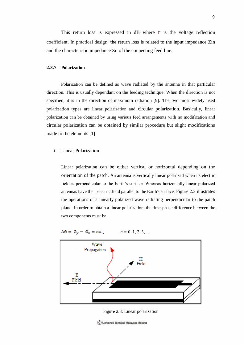
Linear polarization can be either vertical or horizontal depending on the
orientation of the patch. An antenna is vertically linear polarized when its electric
field is perpendicular to the Earth‟s surface. Whereas horizontally linear polarized
antennas have their electric field parallel to the Earth's surface. Figure 2.3 illustrates
the operations of a linearly polarized wave radiating perpendicular to the patch
plane. In order to obtain a linear polarization, the time-phase difference between the
two components must be
, n = 0, 1, 2, 3,…
Figure 2.3: Linear polarization
9

In linear polarization, the quality of the polarization is often inadequate for
application because of the asymmetry of the feed and the radiating element. However, this
purity can be improved by making the arrangement of patches and feed symmetrical.
Examples of antenna radiating with linear polarization using square patch as follow as [7]:
a) Coaxial feed in the middle of one side
b) Direct feed by microstrip line at the middle of one side
c) Feed by a microstrip line across a slot in the ground plane
d) Coaxial feed on one diagonal of the square
e) Direct feed by microstrip line at one corner of the square
f) Feed by a microstrip line across the diagonal slot in the ground plane
ii. Circular Polarization
Circular polarization can result in left hand circularly polarized (LHCP) where
the wave is rotating anticlockwise, or right hand circularly polarized (RHCP) which
denotes a clockwise rotation. In order to obtain a circular polarization, the magnitudes of
the two components are the same and the time- phase difference between them is odd
multiples of . That is
Figure 2.4: Circular polarization
10