A Bust Em’ Out Project - RetroTone · Fuzz . RetroTone® Knowledge, Skills, Supplies and Services...
37
RetroTone® Knowledge, Skills, Supplies and Services A Bust Em’ Out Project The Original 1970’s Jordan Boss Tone This is an original Jordan Boss Tone made in Nashville, TN in the early to mid 70’s by SHO-Sound. Randy California of the band Spirit used the Boss Tone extensively. You can read this article for more information. http://www.vintageguitar.com/19030/jordan-boss-tone/. There were at least 4 versions of the circuit produced. The transistors in our version were non-standard part numbers. One was a Motorola and one was un recognizable all together. Both were extracted from the circuit and measurements were taken. The heart of this clone are the PN2222 and 2N3906 transistors based on this later version. They provide a good approximation of the originals. RetroTone® offers you this kit as our take on a classic. RetroTone® Big Boss Man Fuzz
Transcript of A Bust Em’ Out Project - RetroTone · Fuzz . RetroTone® Knowledge, Skills, Supplies and Services...

RetroTone® Knowledge, Skills, Supplies and Services
A Bust Em’ Out Project The Original
1970’s Jordan Boss Tone
This is an original Jordan Boss Tone made in Nashville, TN in the early to mid 70’s by SHO-Sound. Randy California of the band Spirit used the Boss Tone extensively. You can read this article for more information. http://www.vintageguitar.com/19030/jordan-boss-tone/. There were at least 4 versions of the circuit produced. The transistors in our version were non-standard part numbers. One was a Motorola and one was un recognizable all together. Both were extracted from the circuit and measurements were taken. The heart of this clone are the PN2222 and 2N3906 transistors based on this later version. They provide a good approximation of the originals. RetroTone® offers you this kit as our take on a classic.
RetroTone® Big Boss Man
Fuzz
RetroTone® Knowledge, Skills, Supplies and Services
© 2 0 1 5 R e t r o T o n e , L L C . P a g e 2 | 37
A Bust Em’ Out Project
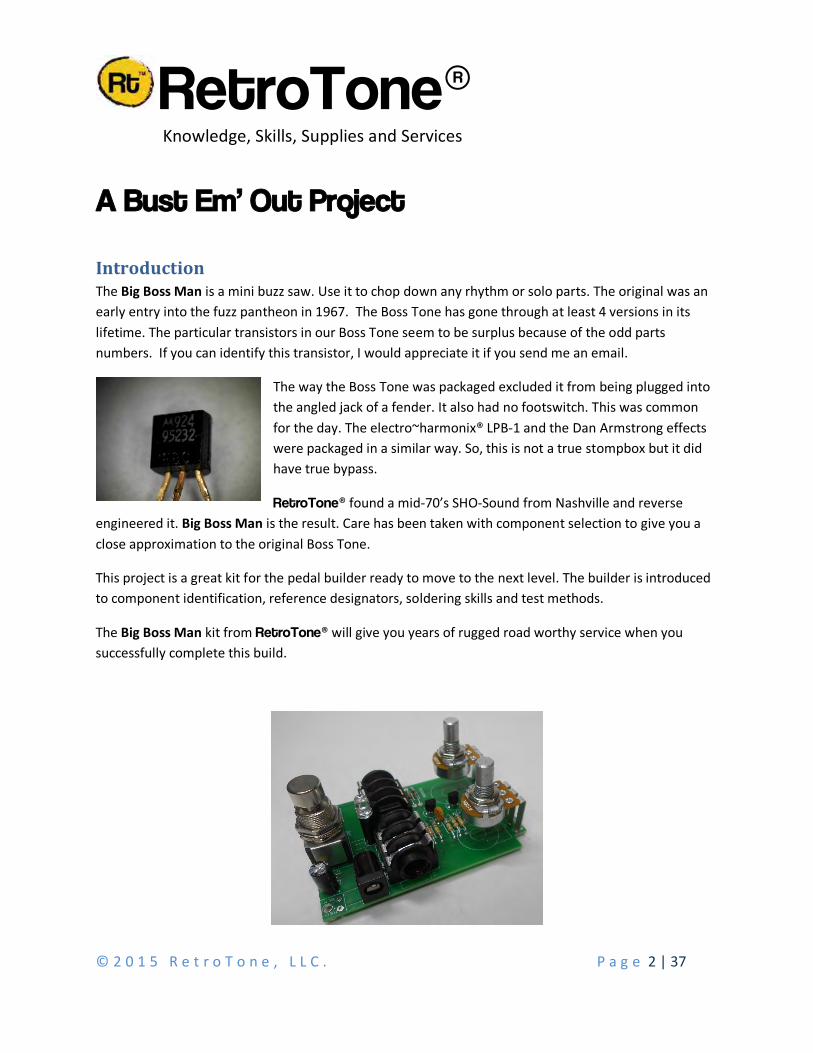
Introduction The Big Boss Man is a mini buzz saw. Use it to chop down any rhythm or solo parts. The original was an early entry into the fuzz pantheon in 1967. The Boss Tone has gone through at least 4 versions in its lifetime. The particular transistors in our Boss Tone seem to be surplus because of the odd parts numbers. If you can identify this transistor, I would appreciate it if you send me an email.
The way the Boss Tone was packaged excluded it from being plugged into the angled jack of a fender. It also had no footswitch. This was common for the day. The electro~harmonix® LPB-1 and the Dan Armstrong effects were packaged in a similar way. So, this is not a true stompbox but it did have true bypass.
RetroTone® found a mid-70’s SHO-Sound from Nashville and reverse engineered it. Big Boss Man is the result. Care has been taken with component selection to give you a close approximation to the original Boss Tone.
This project is a great kit for the pedal builder ready to move to the next level. The builder is introduced to component identification, reference designators, soldering skills and test methods.
The Big Boss Man kit from RetroTone® will give you years of rugged road worthy service when you successfully complete this build.

RetroTone® Knowledge, Skills, Supplies and Services
© 2 0 1 5 R e t r o T o n e , L L C . P a g e 3 | 37
Contents Introduction ............................................................................................................................................ 2
Bill of Materials ....................................................................................................................................... 5
Specifications .......................................................................................................................................... 6
Required Tools ........................................................................................................................................ 6
Parts Placement ...................................................................................................................................... 7
PCB Assembly .......................................................................................................................................... 8
Overview ............................................................................................................................................. 8
Optional Components .......................................................................................................................... 9
Power and I/O Section Assembly ........................................................................................................... 10
Capacitor – C1 ................................................................................................................................... 11
Capacitor – C2 ................................................................................................................................... 15
Resistor - R1 ...................................................................................................................................... 17
Diode – D1 ......................................................................................................................................... 18
Footswitch – SW1 .............................................................................................................................. 20
DC Jack - J3 ........................................................................................................................................ 21
Input/Output Jacks – J1, J2 ................................................................................................................ 22
LED and Standoff – LED1 .................................................................................................................... 23
Battery Snap – BATT1 ........................................................................................................................ 24
Fuzz Circuit Section................................................................................................................................ 26
Resistors R3, R4, R5, R6, R7................................................................................................................ 27
Capacitors C3, C4, C5, C6 ................................................................................................................... 28
Diodes D2, D3 .................................................................................................................................... 28
Transistor Q1, Q2............................................................................................................................... 29
Potentiometer VR1, VR2 .................................................................................................................... 29
Mechanical Assembly ........................................................................................................................ 31
Testing the Big Boss Man ....................................................................................................................... 34
Trouble Shooting Tips ............................................................................................................................ 34
Returns and Exchanges .......................................................................................................................... 37

RetroTone® Knowledge, Skills, Supplies and Services
© 2 0 1 5 R e t r o T o n e , L L C . P a g e 4 | 37
Figure 1 - Completed Big Boss Man .......................................................................................................... 7 Figure 2 – Example Reference Designators on the PCB ............................................................................ 8 Figure 3 – Big Boss Man Assembly ........................................................................................................... 9 Figure 4 - Power and I/O ........................................................................................................................ 10 Figure 5 - Electrolytic Capacitor with Long Positive Lead ........................................................................ 11 Figure 6 - Characteristics of an Electrolytic Capacitor ............................................................................. 12 Figure 7 - Hold the Soldering Iron Tip Under the Lead ............................................................................ 13 Figure 8 - Two Most Common Soldering Mistakes ................................................................................. 14 Figure 9 - Nicely Soldered Capacitor Leads ............................................................................................. 14 Figure 10 - Ceramic Capacitor Markings ................................................................................................. 15 Figure 11 - No Polarity Indication for Capacitor C2 ................................................................................. 15 Figure 12 - C1 and C2 Properly fastened to the PCB ............................................................................... 16 Figure 13 – Resistor – R1 and R2 Value .................................................................................................. 17 Figure 14 - Bending Axial Leads.............................................................................................................. 17 Figure 15 - Diode - D1 Polarity Band ...................................................................................................... 18 Figure 16 - Soldering Resistor and Diode Leads All At Once .................................................................... 19 Figure 17 - Cut Leads After Soldering ..................................................................................................... 19 Figure 18 - Heat Up Footswitch Pin ........................................................................................................ 20 Figure 19 - Footswitch is Flush to PCB .................................................................................................... 20 Figure 20 - DC Jack Alignment on Footprint ........................................................................................... 21 Figure 21 - Large Holes on DC Jack ......................................................................................................... 21 Figure 22 - 1/4" Audio Input/Out Jack .................................................................................................... 22 Figure 23 - LED1 Polarity ........................................................................................................................ 23 Figure 24 - LED and Standoff .................................................................................................................. 23 Figure 25 - LED1 PCB Footprint .............................................................................................................. 23 Figure 26 - Battery Snap PCB Footprint .................................................................................................. 24 Figure 27 – Battery Snap Strain Relief .................................................................................................... 24 Figure 28 - Completed Power and I/O Section........................................................................................ 25 Figure 29 – Completed Big Boss Man ..................................................................................................... 30 Figure 30 - Footswitch Nut Height ......................................................................................................... 31 Figure 31 - Footswitch Washer Stackup ................................................................................................. 31 Figure 32 - Level the PCB ....................................................................................................................... 32 Figure 33 - Center DC Jack Pin In Hole .................................................................................................... 32 Figure 34 – Big Boss Man Completed ..................................................................................................... 33 Figure 35 - Single Hole Dimensions ........................................................................................................ 36

RetroTone® Knowledge, Skills, Supplies and Services
© 2 0 1 5 R e t r o T o n e , L L C . P a g e 5 | 37
Bill of Materials Ref Description Qty Value Part Number
PCB Power Pak 4000-0008 C1 Electrolytic Filter Capacitor 1 100uF 0200-0000 C2 MLCC Ceramic Filter Capacitor 1 10nF 0200-0100 R1, R2 Metal Film Resistor 2 1K 0100-0001 D1 Rectifier Diode 1 1N4001 1400-0001 Big Boss Man PCB Pak 4000-0037 FR4 Printed Circuit Board 1 1200-0007 SW1 Footswitch 1 3PDT 0600-0003 PCB IO Pak 4000-0020 J1, J2 ¼” Input/Out Jacks 2 0900-0002 J3 DC Input PCB Mount 1 0900-0007 BAT1 Battery Snap 1 0900-0001 600-LED Pak 4000-0010 LED1 Yellow Light Emitting Diode 1 5mm LED 1500-0010 0.6” LED Standoff 1 0.1 x 0.6 1600-0004 LED Panel Retainer and Ring 1 1600-0003 Enclosure Pak 4000-0001 1590B Enclosure 1 1000-0006 Adhesive Bumpers 1 1600-0002 Battery Pad 1 1600-0001 Big Boss Man Component Pak 4000-0102 Q1 NPN Bipolar Silicon Transistor 1 PN2222 0700-0010 Q2 NPN Bipolar Silicon Transistor 1 2N3906 0700-0013 R3, R4 Carbon Film 5% 2 18Kohms 0100-0105 R5, R6 Carbon Film 5% 2 560Kohms 0100-0106 R7 Carbon Film 5% 1 150Kohms 0100-0107 C3 Cap Ceramic Disc NPO 1 47pF 0200-0104 C4, C5, C6 Cap Ceramic Disc Z5U 3 10nF 0200-0102 D1, D2 Signal Diode 2 1N914 1400-0003 Big Boss Man Dial Indicator Pak 4000-0202 VR1, VR2 Potentiometer Audio Taper, Right Angle PCB 2 100Kohms 0500-0051 Black Knob 2 1100-0002

RetroTone® Knowledge, Skills, Supplies and Services
© 2 0 1 5 R e t r o T o n e , L L C . P a g e 6 | 37
Specifications High Quality FR4 PCB Input Impedance 56Kohms 9VDC Input DC Supply Output Impedance 15Kohms Frequency Response 20Hz- 20kHz Current Draw 7.5mA@9VDC
Required Tools • 6” Needle Nose Pliers • Small flat blade screw driver • Phillips Screw Driver • 4” Wire Cutters • Soldering Iron • Solder – No Clean Flux - 0.031” • Wet Sponge

RetroTone® Knowledge, Skills, Supplies and Services
© 2 0 1 5 R e t r o T o n e , L L C . P a g e 7 | 37
Parts Placement It is important to place the correct component in the correct location on the printed circuit board (PCB). This section helps the builder just starting out visually identify the component and how it is placed and attached to the PCB.
Figure 1 - Completed Big Boss Man
Each component has a reference designator. A reference designator has one or more letters followed by a number. This scheme is standard throughout the electronics industry.
• Resistors - Rx • Capacitors – Cx • Diode – Dx • Transistors Qx • Connecters - Jx • Switches - SWx • Battery Snap – BATx • Light Emitting Diode – LEDx

RetroTone® Knowledge, Skills, Supplies and Services
© 2 0 1 5 R e t r o T o n e , L L C . P a g e 8 | 37
Some components have a “polarity” and must be placed correctly for the component to work properly. The Transistor, LED, diode, some capacitors and the battery snap on the Big Boss Man have a polarity. The photos below show the LED with a clearly marked “polarity.” The flat side of the LED is the “negative” terminal. The small rectangle on D1 shows the “polarity” for a diode. This terminal is called a cathode. The small plus sign on capacitor C1 shows the “positive” terminal.
Figure 2 – Example Reference Designators on the PCB
PCB Assembly
Overview Start with the resistors, capacitors and the diode. These components lie close to the board and can be difficult to place if there are large components in close proximity. Be aware of the polarity of the filter cap and the diode.
The footswitch is next. The only trick to this component is to make sure that it is flush with the board.
Next, place the DC Jack. This component has large holes and requires a significant amount of solder to fill the holes. It also sits very close to the ¼” input jack. It is very important to make sure that the DC jack aligns with the footprint pattern on the PCB. It also must sit flush with the PCB. Proper placement allows the DC jack to align with the holes in the enclosure in the final assembly.
Place the ¼” jacks. Make sure the open end of the connector is facing the outside edge of the board. The pattern is symetrical so it is easy to put it in backwards (yes, I’ve done it). This must also be flush with the board.
Put the stand off on the led and solder it into the pattern observing that the polarity is correct. The flat side of the LED is the negative terminal and it must align with the footprint on the PCB. Be sure that it is standing straight. This is essential to provide proper alignment with the hole in the enclosure.

RetroTone® Knowledge, Skills, Supplies and Services
© 2 0 1 5 R e t r o T o n e , L L C . P a g e 9 | 37
Finally, the battery snap leads should be put into the large hole from underneath the PCB then each lead soldered into the respective hole. This provides a strain releif if the snap is acidently tugged. The PCB is clearly marked with the positive and negative terminals, as well as, lead colors.
Optional Components The battery snap and the reverse polarity protection are optional. If you intend to always use your pedal with a power source on a pedal board you don’t really need the battery snap. The Big Boss Man circuit is built with discrete transistors, you really don’t need the reverse polarity circuit. If you think about it for a second, the transistors really act as diodes and suffer no dammage from reverse polarity. However, you can dammage the transistor with over voltage or a poor bias scheme.
Figure 3 – Big Boss Man Assembly

RetroTone® Knowledge, Skills, Supplies and Services
© 2 0 1 5 R e t r o T o n e , L L C . P a g e 10 | 37
Power and I/O Section Assembly
Figure 4 - Power and I/O
RetroTone® Knowledge, Skills, Supplies and Services
© 2 0 1 5 R e t r o T o n e , L L C . P a g e 11 | 37
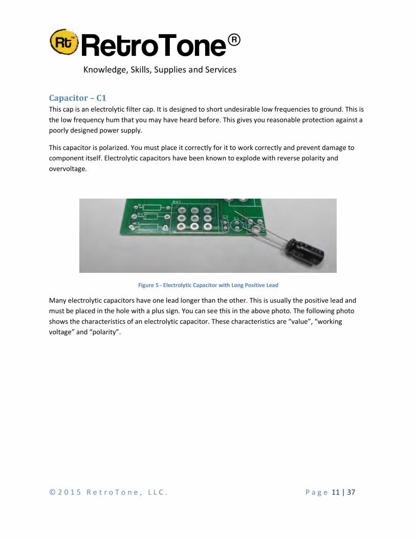
Capacitor – C1 This cap is an electrolytic filter cap. It is designed to short undesirable low frequencies to ground. This is the low frequency hum that you may have heard before. This gives you reasonable protection against a poorly designed power supply.
This capacitor is polarized. You must place it correctly for it to work correctly and prevent damage to component itself. Electrolytic capacitors have been known to explode with reverse polarity and overvoltage.
Figure 5 - Electrolytic Capacitor with Long Positive Lead
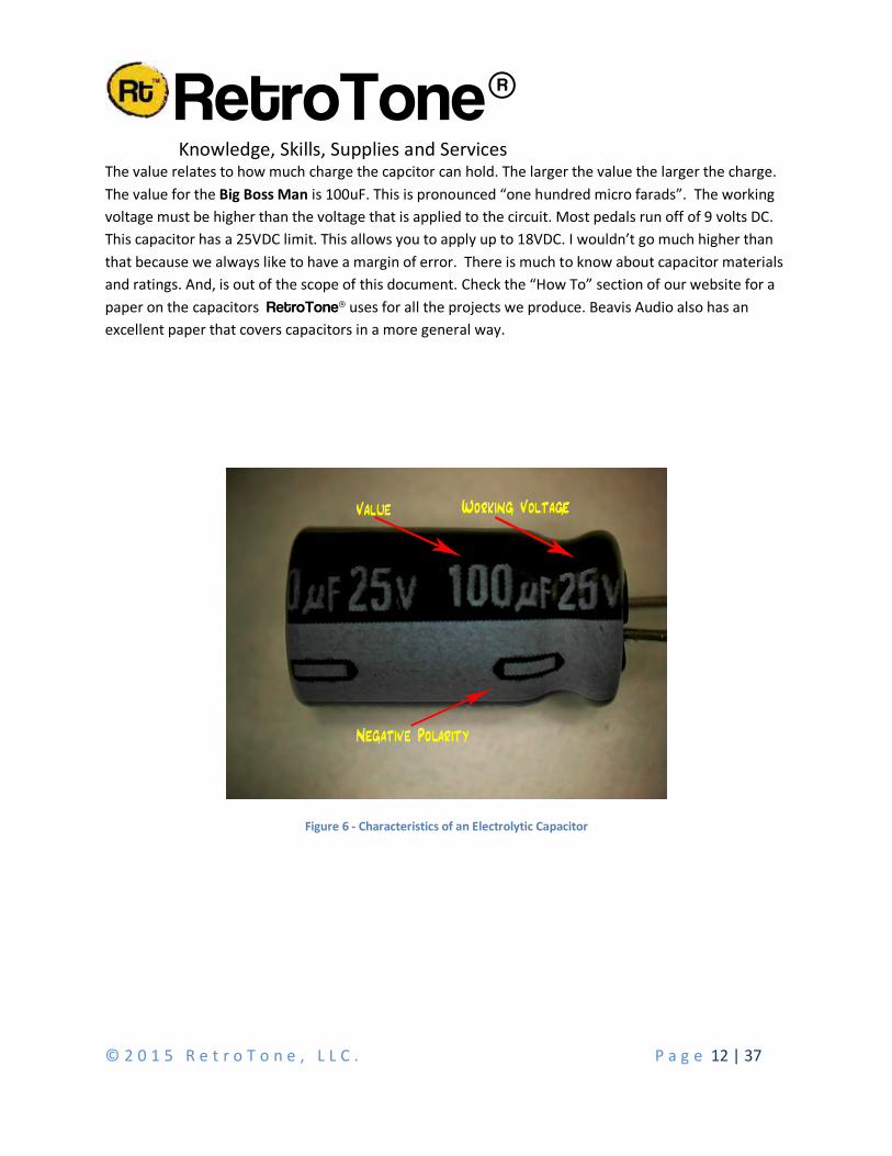
Many electrolytic capacitors have one lead longer than the other. This is usually the positive lead and must be placed in the hole with a plus sign. You can see this in the above photo. The following photo shows the characteristics of an electrolytic capacitor. These characteristics are “value”, “working voltage” and “polarity”.
RetroTone® Knowledge, Skills, Supplies and Services
© 2 0 1 5 R e t r o T o n e , L L C . P a g e 12 | 37
The value relates to how much charge the capcitor can hold. The larger the value the larger the charge. The value for the Big Boss Man is 100uF. This is pronounced “one hundred micro farads”. The working voltage must be higher than the voltage that is applied to the circuit. Most pedals run off of 9 volts DC. This capacitor has a 25VDC limit. This allows you to apply up to 18VDC. I wouldn’t go much higher than that because we always like to have a margin of error. There is much to know about capacitor materials and ratings. And, is out of the scope of this document. Check the “How To” section of our website for a paper on the capacitors RetroTone® uses for all the projects we produce. Beavis Audio also has an excellent paper that covers capacitors in a more general way.
Figure 6 - Characteristics of an Electrolytic Capacitor
RetroTone® Knowledge, Skills, Supplies and Services
© 2 0 1 5 R e t r o T o n e , L L C . P a g e 13 | 37
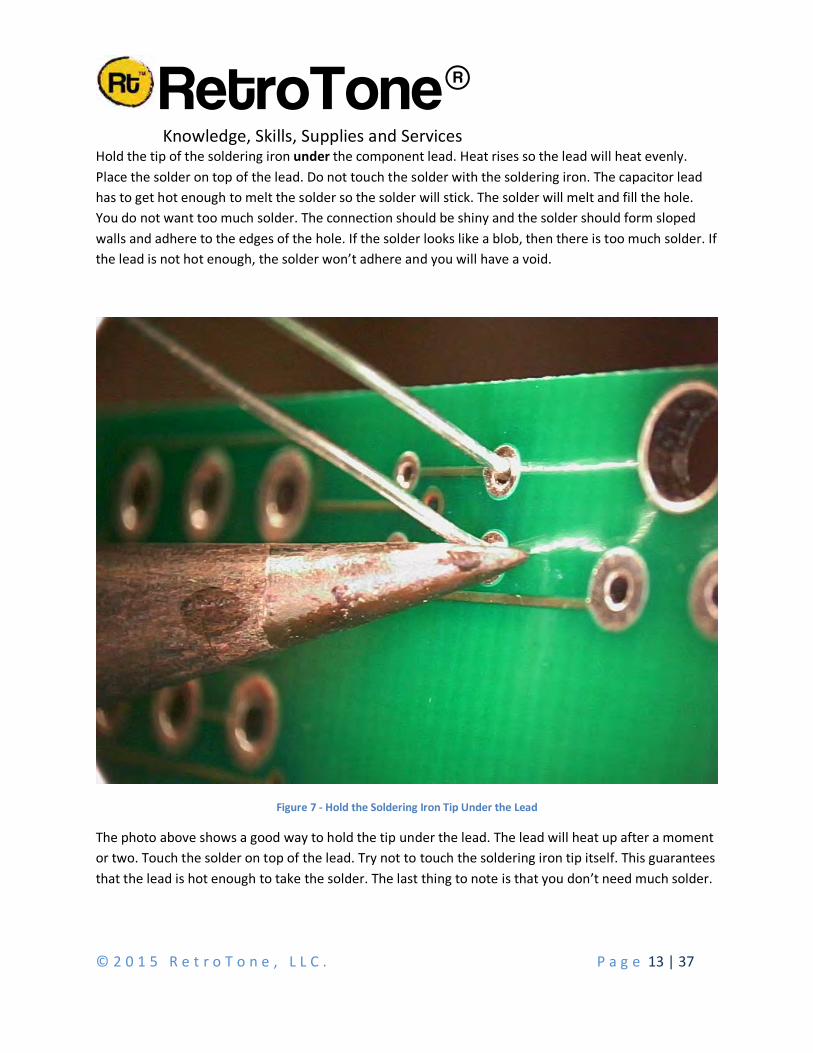
Hold the tip of the soldering iron under the component lead. Heat rises so the lead will heat evenly. Place the solder on top of the lead. Do not touch the solder with the soldering iron. The capacitor lead has to get hot enough to melt the solder so the solder will stick. The solder will melt and fill the hole. You do not want too much solder. The connection should be shiny and the solder should form sloped walls and adhere to the edges of the hole. If the solder looks like a blob, then there is too much solder. If the lead is not hot enough, the solder won’t adhere and you will have a void.
Figure 7 - Hold the Soldering Iron Tip Under the Lead
The photo above shows a good way to hold the tip under the lead. The lead will heat up after a moment or two. Touch the solder on top of the lead. Try not to touch the soldering iron tip itself. This guarantees that the lead is hot enough to take the solder. The last thing to note is that you don’t need much solder.
RetroTone® Knowledge, Skills, Supplies and Services
© 2 0 1 5 R e t r o T o n e , L L C . P a g e 14 | 37
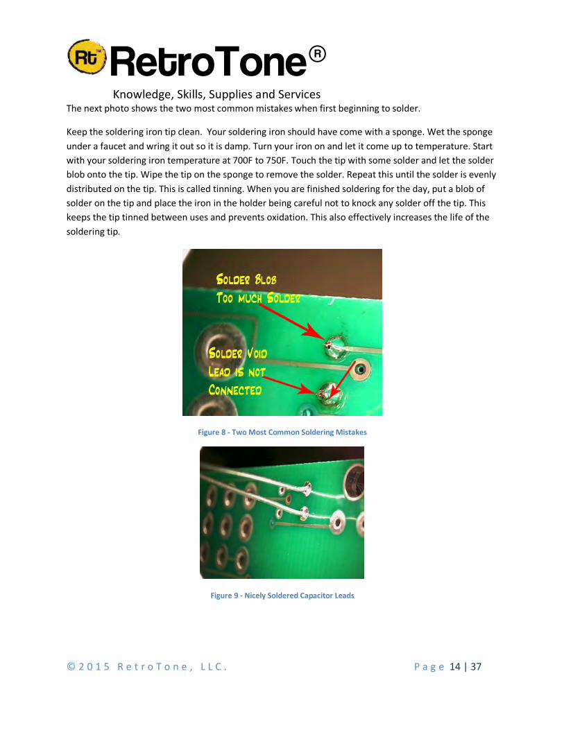
The next photo shows the two most common mistakes when first beginning to solder.
Keep the soldering iron tip clean. Your soldering iron should have come with a sponge. Wet the sponge under a faucet and wring it out so it is damp. Turn your iron on and let it come up to temperature. Start with your soldering iron temperature at 700F to 750F. Touch the tip with some solder and let the solder blob onto the tip. Wipe the tip on the sponge to remove the solder. Repeat this until the solder is evenly distributed on the tip. This is called tinning. When you are finished soldering for the day, put a blob of solder on the tip and place the iron in the holder being careful not to knock any solder off the tip. This keeps the tip tinned between uses and prevents oxidation. This also effectively increases the life of the soldering tip.
Figure 8 - Two Most Common Soldering Mistakes
Figure 9 - Nicely Soldered Capacitor Leads

RetroTone® Knowledge, Skills, Supplies and Services
© 2 0 1 5 R e t r o T o n e , L L C . P a g e 15 | 37
Capacitor – C2 This capacitor is multilayer ceramic capacitor (MLCC). It is designed to short undesirable high frequencies to ground. Such as higher frequency radio signals.
Figure 10 - Ceramic Capacitor Markings
Figure 11 - No Polarity Indication for Capacitor C2

RetroTone® Knowledge, Skills, Supplies and Services
© 2 0 1 5 R e t r o T o n e , L L C . P a g e 16 | 37
The electrolytic (C1) we placed can successfully short low frequencies but its effectiveness drops off as the frequencies get higher. Pairing C1 and C2 filters out a broad range of frequencies from the power supply.
The MLCC capacitor is marked with two items. One is the manufacturer’s mark, in this case BC, for BC Components made by Vishay. The other is the value marked as 104. What this means is a 10 followed by 4 zeroes. This comes out to 100000. But 100000 what? This value is in pico farads. This is an industry standard marking. We have all agreed that the value is in pico farads for this type of capacitor. There are three value ranges commonly used in capacitors this size. “Mili” is not used for capacitors but is shown here for completeness. They are as follows.
Engineering Notation Pico p 10-12 0.000000000000 Nano n 10-9 0.000000000 Micro u 10-6 0.000000 Milli m 10-3 0.000
With all those zeroes and a decimal point, it is much easier to write 0.1uF than 100000pF. This value is also equivalent to 100nF. These are all equivalent for the value on our capacitor. Some people don’t like the decimal point in 0.1uF because it can get lost in the document duplication process so they will use 100nF for clarity. 100000pF just has too many zeroes.
Figure 12 - C1 and C2 Properly fastened to the PCB

RetroTone® Knowledge, Skills, Supplies and Services
© 2 0 1 5 R e t r o T o n e , L L C . P a g e 17 | 37
Resistor - R1 This resistor controls the amount of current that flows through the LED. The photo below shows the value of the resistor supplied with your kit. This resistor is a metal film. Metal film resistors are stable over temperature and are available with tight tolerances. The photo below shows the value. The manufacturer has designed this code and is not necessarily an industry standard. The 100 is the value, the 1 is the number of zeroes and the F is the tolerance. This resistor is 1000 Ohms with a tolerance of 1%. You can also call this a 1K Ohm resistor.
Before the resistor can be placed in the footprint on the board, the leads must be bent. It is important to not bend the lead right next to the package. The lead can break off inside the package or crack the package. Use your needle noise pliers as shown in the photo below. Hold the pliers tip next to the package then bend the lead to produce a nice sharp 90 degree angle.
Figure 13 – Resistor – R1 and R2 Value
Figure 14 - Bending Axial Leads
The LED current is determined by Resistor - R1. The more current through the LED---the brighter. The LED in the Big Boss Man has current rating of 20mA for maximum brightness. Personally, I don’t like super bright LEDs in a night club situation. Some of the LEDs are so bright; I cannot see the effect panel. The current in this LED is 7mA. This is bright enough to see it but not so bright that you can’t see anything on the pedal.
RetroTone® Knowledge, Skills, Supplies and Services
© 2 0 1 5 R e t r o T o n e , L L C . P a g e 18 | 37
Calculate LED current with this equation. (V+ - VF )/ R1. V+ = 9V, VF is the forward voltage of the LED. This is minimum voltage require to make the LED start conducting. This LED has a forward voltage of 2.1Volts. And, R1 is 1000.
(9 – 2.1)/1000 = 0.0069A or 6.9mA. The resistor to use for maximum brightness would be as follows.
(9-2.1)/0.020 = 345 ohms. This is not a standard 1% resistor value. The nearest value is 348 ohms. 0.020 is another way to write 20mA.
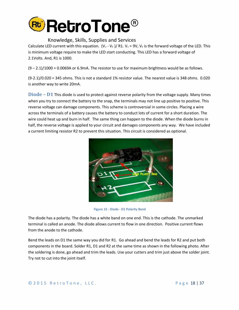
Diode – D1 This diode is used to protect against reverse polarity from the voltage supply. Many times when you try to connect the battery to the snap, the terminals may not line up positive to positive. This reverse voltage can damage components. This scheme is controversial in some circles. Placing a wire across the terminals of a battery causes the battery to conduct lots of current for a short duration. The wire could heat up and burn in half. The same thing can happen to the diode. When the diode burns in half, the reverse voltage is applied to your circuit and damages components any way. We have included a current limiting resistor R2 to prevent this situation. This circuit is considered as optional.
Figure 15 - Diode - D1 Polarity Band
The diode has a polarity. The diode has a white band on one end. This is the cathode. The unmarked terminal is called an anode. The diode allows current to flow in one direction. Positive current flows from the anode to the cathode.
Bend the leads on D1 the same way you did for R1. Go ahead and bend the leads for R2 and put both components in the board. Solder R1, D1 and R2 at the same time as shown in the following photo. After the soldering is done, go ahead and trim the leads. Use your cutters and trim just above the solder joint. Try not to cut into the joint itself.

RetroTone® Knowledge, Skills, Supplies and Services
© 2 0 1 5 R e t r o T o n e , L L C . P a g e 19 | 37
Figure 16 - Soldering Resistor and Diode Leads All At Once
Figure 17 - Cut Leads After Soldering

RetroTone® Knowledge, Skills, Supplies and Services
© 2 0 1 5 R e t r o T o n e , L L C . P a g e 20 | 37
Footswitch – SW1 All the soldering principles you have learned up till now apply to the footswitch as well. Hold the soldering iron on the pin of the footswitch to get it hot enough to take the solder. The main consideration for the footswitch is to make sure it is flush to the PCB. Solder one hole and make sure the footswitch is flush with the PCB. Solder the rest of the holes being sure that the footswitch remains flush to the PCB.
Figure 18 - Heat Up Footswitch Pin
Figure 19 - Footswitch is Flush to PCB
RetroTone® Knowledge, Skills, Supplies and Services
© 2 0 1 5 R e t r o T o n e , L L C . P a g e 21 | 37
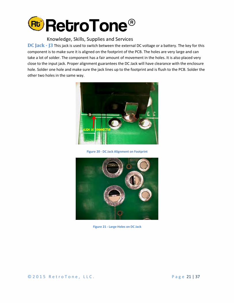
DC Jack - J3 This jack is used to switch between the external DC voltage or a battery. The key for this component is to make sure it is aligned on the footprint of the PCB. The holes are very large and can take a lot of solder. The component has a fair amount of movement in the holes. It is also placed very close to the input jack. Proper alignment guarantees the DC Jack will have clearance with the enclosure hole. Solder one hole and make sure the jack lines up to the footprint and is flush to the PCB. Solder the other two holes in the same way.
Figure 20 - DC Jack Alignment on Footprint
Figure 21 - Large Holes on DC Jack

RetroTone® Knowledge, Skills, Supplies and Services
© 2 0 1 5 R e t r o T o n e , L L C . P a g e 22 | 37
Input/Output Jacks – J1, J2 Both of these components are identical. Either one will work in either position. Make sure you solder it in with the opening facing out from the PCB. Solder one hole then make sure the jack is flush with the PCB. Then solder another hole, and check that the jack is still flush. Then solder the other holes. Make sure that the connector is flush to the PCB. The opening needs to align with the enclosure hole.
Figure 22 - 1/4" Audio Input/Out Jack

RetroTone® Knowledge, Skills, Supplies and Services
© 2 0 1 5 R e t r o T o n e , L L C . P a g e 23 | 37
LED and Standoff – LED1 LED1 is another component on the Big Boss Man with a polarity. Place the standoff on the LED and solder it in observing that the flat side lines up with the “-“ on the PCB. The LED should be standing as straight and perpendicular to the PCB as possible. There is a decent amount of tolerance on the enclosure it the LED alignment isn’t perfect.
Figure 23 - LED1 Polarity
Figure 24 - LED and Standoff
Figure 25 - LED1 PCB Footprint

RetroTone® Knowledge, Skills, Supplies and Services
© 2 0 1 5 R e t r o T o n e , L L C . P a g e 24 | 37
Battery Snap – BATT1 The battery snap footprint provides a simple strain relief. The battery snap leads should be put into the large hole from underneath the PCB then each lead soldered into the respective hole. This provides a strain releif if the snap is acidently tugged. The PCB is clearly marked with the positive and negative terminals, as well as, lead colors.
Again, just a small amount of solder goes a long way. The battery snap leads are pre-tinned so try not to heat the leads too much as the insulation will melt.
Figure 26 - Battery Snap PCB Footprint
Figure 27 – Battery Snap Strain Relief
RetroTone® Knowledge, Skills, Supplies and Services
© 2 0 1 5 R e t r o T o n e , L L C . P a g e 25 | 37
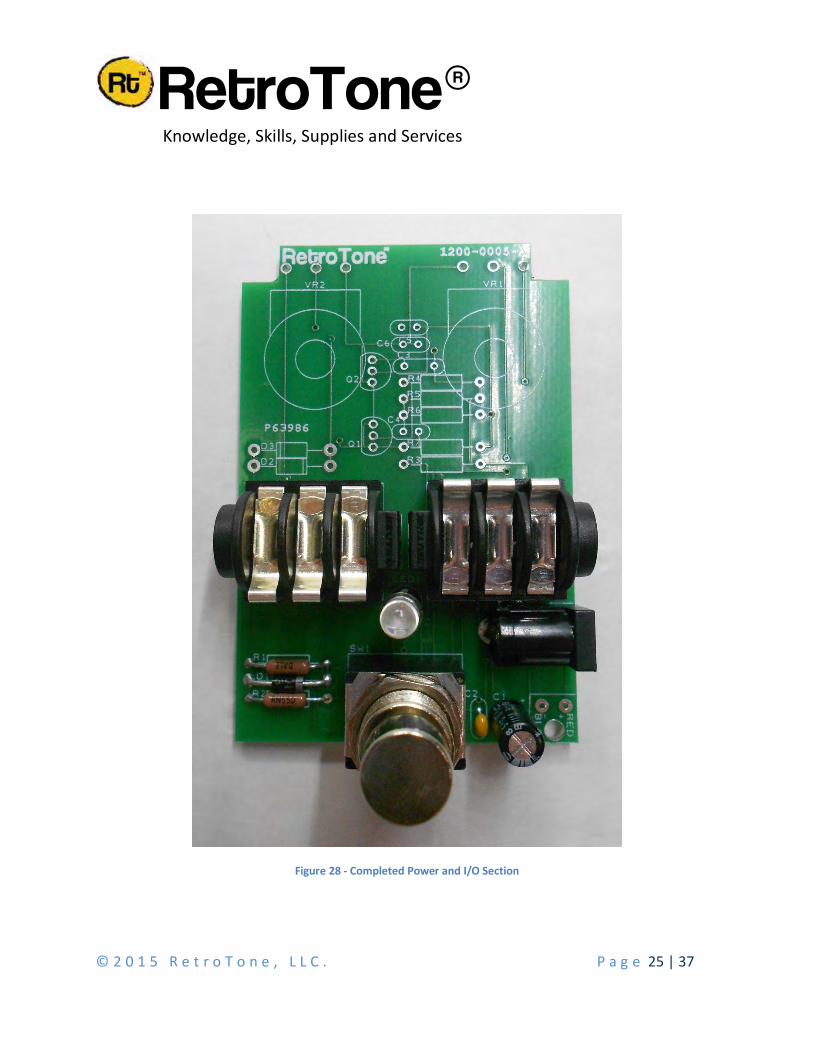
Figure 28 - Completed Power and I/O Section

RetroTone® Knowledge, Skills, Supplies and Services
© 2 0 1 5 R e t r o T o n e , L L C . P a g e 26 | 37
Fuzz Circuit Section

RetroTone® Knowledge, Skills, Supplies and Services
© 2 0 1 5 R e t r o T o n e , L L C . P a g e 27 | 37
Resistors R3, R4, R5, R6, R7 These resistors are carbon composition resistors just like the original Boss Tone®. They provide bias, gain, feedback and input impedance and output impedance for the transistors. Each resistor has a set of color bands that represent the value and tolerance of the resistor. Bend the leads just like the LED resistor and diode.
R3, R4 = 18K, brown, gray, orange, gold
R5, R6 = 560K, green, blue, yellow, gold
R7 = 150K, brown, green, yellow, gold

RetroTone® Knowledge, Skills, Supplies and Services
© 2 0 1 5 R e t r o T o n e , L L C . P a g e 28 | 37
Capacitors C3, C4, C5, C6 Capacitors are ceramic disc. The frequency and value are very stable value over temperature. These capacitors are not polarized so placement is more aesthetics than functional. The PCB outline reflects the shape of the cap.
C3 = 47pF
C4, C5, C6 = 10nF = 0.01uF
Diodes D2, D3 These diodes provide clipping for that distinctive buzz. Polarity is important so observe the band on the PCB outline and place the black band of the diode correctly. The diodes are a popular component to mod. Some people use LEDs or germanium diodes for a different sound. We used 1n914 signal diodes to be faithful to the original design.

RetroTone® Knowledge, Skills, Supplies and Services
© 2 0 1 5 R e t r o T o n e , L L C . P a g e 29 | 37
Transistor Q1, Q2 The 2N3906 transistor is a PNP small signal, medium gain silicon device. The transistor can handle continuous currents of 200mA and dissipate 625mW. It is similar to the type found in the Boss Tone® we reverse engineered. The PN2222 is a plastic case version of its cousin the 2N2222. It is a medium gain NPN silicon device that can handle a whopping 500mA of collector current and dissipate 625mW.
Leave some lead length between the transistor and the PCB. This allows you to get a test probe on the leads.
Q1 = 2N3906. PNP Bipolar Junction Transistor
Q2 = PN2222, NPN Bipolar Junction Transistor
Potentiometer VR1, VR2 The potentiometers come with an alignment tab that needs to be removed. It is designed to be snapped off. It should come off with a gentle twist. The leads on the potentiometer are large and require a little time to heat up to allow the solder to flow. Be sure the potentiometer is parallel to the PCB.

RetroTone® Knowledge, Skills, Supplies and Services
© 2 0 1 5 R e t r o T o n e , L L C . P a g e 30 | 37
Figure 29 – Completed Big Boss Man
RetroTone® Knowledge, Skills, Supplies and Services
© 2 0 1 5 R e t r o T o n e , L L C . P a g e 31 | 37
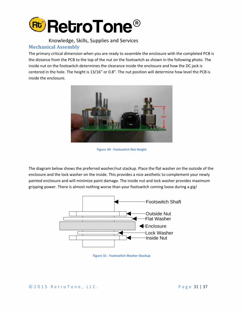
Mechanical Assembly The primary critical dimension when you are ready to assemble the enclosure with the completed PCB is the distance from the PCB to the top of the nut on the footswitch as shown in the following photo. The inside nut on the footswitch determines the clearance inside the enclosure and how the DC jack is centered in the hole. The height is 13/16” or 0.8”. The nut position will determine how level the PCB is inside the enclosure.
Figure 30 - Footswitch Nut Height
The diagram below shows the preferred washer/nut stackup. Place the flat washer on the outside of the enclosure and the lock washer on the inside. This provides a nice aesthetic to complement your newly painted enclosure and will minimize paint damage. The inside nut and lock washer provides maximum gripping power. There is almost nothing worse than your footswitch coming loose during a gig!
Footswitch Shaft
Outside Nut
Inside NutLock WasherEnclosureFlat Washer
Figure 31 - Footswitch Washer Stackup

RetroTone® Knowledge, Skills, Supplies and Services
© 2 0 1 5 R e t r o T o n e , L L C . P a g e 32 | 37
The ¼” input/output connectors provide a pivot point for the PCB. A couple of tries may be necessary to get the PCB level with the enclosure and square things up.
Figure 32 - Level the PCB
An indication that everything is lined up properly is the DC jack will be centered in the hole.
Figure 33 - Center DC Jack Pin In Hole
Don’t tighten anything down until the PCB fits right and is level. Tighten the footswitch first then the Input/Output jacks then the potentiometer last. Check the spacing between the PCB and the wall of the enclosure to make sure it is evenly spaced. There should be a slight gap between the PCB and the enclosure. Don’t forget to finish the build with the exterior LED retainer bushing. The interior LED retainer ring is not used.

RetroTone® Knowledge, Skills, Supplies and Services
© 2 0 1 5 R e t r o T o n e , L L C . P a g e 33 | 37
Figure 34 – Big Boss Man Completed
RetroTone® Knowledge, Skills, Supplies and Services
© 2 0 1 5 R e t r o T o n e , L L C . P a g e 34 | 37
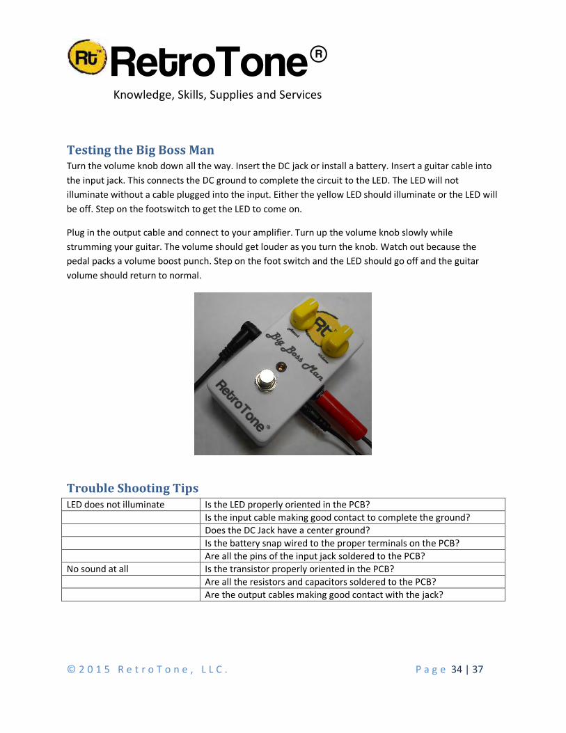
Testing the Big Boss Man Turn the volume knob down all the way. Insert the DC jack or install a battery. Insert a guitar cable into the input jack. This connects the DC ground to complete the circuit to the LED. The LED will not illuminate without a cable plugged into the input. Either the yellow LED should illuminate or the LED will be off. Step on the footswitch to get the LED to come on.
Plug in the output cable and connect to your amplifier. Turn up the volume knob slowly while strumming your guitar. The volume should get louder as you turn the knob. Watch out because the pedal packs a volume boost punch. Step on the foot switch and the LED should go off and the guitar volume should return to normal.
Trouble Shooting Tips LED does not illuminate Is the LED properly oriented in the PCB? Is the input cable making good contact to complete the ground? Does the DC Jack have a center ground? Is the battery snap wired to the proper terminals on the PCB? Are all the pins of the input jack soldered to the PCB? No sound at all Is the transistor properly oriented in the PCB? Are all the resistors and capacitors soldered to the PCB? Are the output cables making good contact with the jack?

RetroTone® Knowledge, Skills, Supplies and Services
© 2 0 1 5 R e t r o T o n e , L L C . P a g e 35 | 37

RetroTone® Knowledge, Skills, Supplies and Services
© 2 0 1 5 R e t r o T o n e , L L C . P a g e 36 | 37
Figure 35 - Single Hole Dimensions
This drawing may not be to scale.
Potentiometer clearance hole 0.2953” = 7.5mm

RetroTone® Knowledge, Skills, Supplies and Services
© 2 0 1 5 R e t r o T o n e , L L C . P a g e 37 | 37
Returns and Exchanges
Log into your account, find the original order and follow the online instructions to start the RMA process.
Parts that are defective or parts that are missing from the kits will be replaced up to 30 days from the date of purchase. Include the defective/missing part numbers in the comments field during the RMA process.
We will gladly accept the return of kits for a full refund for 15 days from the date of purchase.
• The buyer is responsible for return shipping on all returned orders. • Returned orders that do not have an RMA number will be declined. • Orders returned that are not in the original packaging will be charged a 15% restocking fee. • Orders returned that are not in the original packaging and missing parts will be declined. • Orders that have been used (the assembly process has been started) cannot be returned for any reason. • Partial refunds are not allowed.