A 45nm CMOS, low jitter, all-digital delayed locked loop ...933/fulltext.pdf · Acknowledgements I...
75
A 45nm CMOS, Low Jitter, All-Digital Delay Locked Loop with a Circuit to Dynamically Vary Phase to Achieve Fast Lock A Thesis Presented by Soumya Shivakumar Begur to The Department of Electrical and Computer Engineering in partial fulfillment of the requirements for the degree of Master of Science in Electrical and Computer Engineering Northeastern University Boston, Massachusetts October 2011
Transcript of A 45nm CMOS, low jitter, all-digital delayed locked loop ...933/fulltext.pdf · Acknowledgements I...

A 45nm CMOS, Low Jitter, All-Digital Delay Locked Loopwith a Circuit to Dynamically Vary Phase to Achieve Fast Lock
A Thesis Presentedby
Soumya Shivakumar Begur
to
The Department of Electrical and Computer Engineering
in partial fulfillment of the requirementsfor the degree of
Master of Science
in
Electrical and Computer Engineering
Northeastern UniversityBoston, Massachusetts
October 2011

NORTHEASTERN UNIVERSITYGraduate School of Engineering
Thesis Title: A 45nm CMOS, Low Jitter, All-Digital Delay Locked Loopwith a Circuit to Dynamically Vary Phase to Achieve Fast Lock.
Author: Soumya Shivakumar Begur.
Department: Electrical and Computer Engineering.
Approved for Thesis Requirements of the Master of Science Degree
Thesis Advisor: Prof. Yong-Bin Kim Date
Thesis Reader: Prof. Fabrizio Lombardi Date
Thesis Reader: Prof. Gunar Schirner Date
Department Chair: Prof. Ali Abur Date
Director of the Graduate School:
Dean: Prof. Sara Wadia-Fascetti Date

Abstract
The objective of the thesis is to address the problem of clock skew between two different clock
domains in modern day microprocessors due to the process, voltage and temperature (PVT)
variations. In order to mitigate the misalignment of the clocks in the different clock domains, a
delay line is added in all but the reference clock domain. These delay lines add or subtract the
delay (as necessary) to keep the clocks continuously aligned to a common reference clock delay.
This ensures error free data transfer between any two clock domains.
A novel Digital DLL design is proposed to achieve short locking time by having a separate
circuitry for fast lock in the DLL. The fast lock mechanism can be switched off and the power
dissipation can be returned to normal levels after the DLL has locked. A separate fine-delay
block makes the proposed DLL have ultra-low jitter after lock. The results show that the
proposed DLL, implemented in 45nm CMOS technology, needs only 24 cycles to correct (i.e. to
lock) for 500ps clock skew when compared to more than 38 lock cycles for a conventional DLL
without the fast lock mechanism. A Monte-Carlo simulation yielded a RMS jitter and peak-
to-peak jitter values after lock of 5.26ps and 10.57ps respectively. Average power consumption
before lock is <425µW with this number falling to <335µW after lock. The frequency of
operation of the proposed DLL is 280MHz - 1.63GHz and can be used for a variety of applications
which require precise time intervals.

Acknowledgements
I would like to express my deepest gratitude to my advisor, Prof. Yong-Bin Kim for his
guidance and encouragement. I am extremely grateful for his help and support throughout my
graduate school experience. Without his valuable suggestions and assistance, this thesis would
not have been possible.
I would like to thank my brother-in-law, Mr. Sompur Shivakumar for his constant en-
couragement and evincing keen interest in my thesis. I am grateful for his valuable advice,
motivation and support throughout my graduate career.
I would also like to thank my friends for their suggestions and support.
Finally, I would like to express my profound thanks to my beloved parents, Dr. B. S.
Shivakumar and Kalpana Shivakumar, and my sister, Dr. Shilpa Shivakumar, who encouraged
me continuously and stood by me throughout my studies. I would not have made it through
the toughest times without their support.
Soumya S. BegurOctober 2011

Contents
1 Introduction 11.1 Delay Locked Loop Overview . . . . . . . . . . . . . . . . . . . . . . . . . . . . . 3
1.1.1 Analog DLL . . . . . . . . . . . . . . . . . . . . . . . . . . . . . . . . . . . 41.1.2 Digital DLL . . . . . . . . . . . . . . . . . . . . . . . . . . . . . . . . . . . 51.1.3 Comparison between Analog DLL and Digital DLL . . . . . . . . . . . . . 5
1.2 Conclusion . . . . . . . . . . . . . . . . . . . . . . . . . . . . . . . . . . . . . . . 6
2 Design of a Digital DLL 72.1 Phase Detector . . . . . . . . . . . . . . . . . . . . . . . . . . . . . . . . . . . . . 82.2 Control Mechanism . . . . . . . . . . . . . . . . . . . . . . . . . . . . . . . . . . . 102.3 Digital Controlled Delay Line . . . . . . . . . . . . . . . . . . . . . . . . . . . . . 11
2.3.1 Coarse Delay Line . . . . . . . . . . . . . . . . . . . . . . . . . . . . . . . 112.3.2 Fine Delay Line . . . . . . . . . . . . . . . . . . . . . . . . . . . . . . . . . 13
2.4 Conclusion . . . . . . . . . . . . . . . . . . . . . . . . . . . . . . . . . . . . . . . 15
3 Design of Proposed Fast Lock Digital DLL 163.1 Design Flow of the DLL controller . . . . . . . . . . . . . . . . . . . . . . . . . . 173.2 Phase Detector . . . . . . . . . . . . . . . . . . . . . . . . . . . . . . . . . . . . . 193.3 Controller . . . . . . . . . . . . . . . . . . . . . . . . . . . . . . . . . . . . . . . . 21
3.3.1 Binary Up-Down Counter . . . . . . . . . . . . . . . . . . . . . . . . . . . 213.3.1.1 5-Bit Up-Down Counter . . . . . . . . . . . . . . . . . . . . . . . 213.3.1.2 4-Bit Up-Down Counter . . . . . . . . . . . . . . . . . . . . . . . 26
3.3.2 Fast Lock Mechanism . . . . . . . . . . . . . . . . . . . . . . . . . . . . . 303.3.2.1 Fast Lock Block . . . . . . . . . . . . . . . . . . . . . . . . . . . 313.3.2.2 Encoder . . . . . . . . . . . . . . . . . . . . . . . . . . . . . . . . 373.3.2.3 Encoder Flip-Flop . . . . . . . . . . . . . . . . . . . . . . . . . . 39
3.3.3 Adder . . . . . . . . . . . . . . . . . . . . . . . . . . . . . . . . . . . . . . 393.3.4 Lock Detector . . . . . . . . . . . . . . . . . . . . . . . . . . . . . . . . . . 403.3.5 Adder Flip-Flop block . . . . . . . . . . . . . . . . . . . . . . . . . . . . . 423.3.6 Select . . . . . . . . . . . . . . . . . . . . . . . . . . . . . . . . . . . . . . 423.3.7 Decoder . . . . . . . . . . . . . . . . . . . . . . . . . . . . . . . . . . . . . 43
3.4 Digital Controlled Delay Line . . . . . . . . . . . . . . . . . . . . . . . . . . . . . 463.4.1 Coarse Delay Line . . . . . . . . . . . . . . . . . . . . . . . . . . . . . . . 463.4.2 Fine Delay Line . . . . . . . . . . . . . . . . . . . . . . . . . . . . . . . . . 47
3.4.2.1 Fine Delay Block . . . . . . . . . . . . . . . . . . . . . . . . . . . 483.4.2.2 16-bit Multiplexer . . . . . . . . . . . . . . . . . . . . . . . . . . 51
i

3.5 Conclusion . . . . . . . . . . . . . . . . . . . . . . . . . . . . . . . . . . . . . . . 52
4 Results and Performance Analysis 53
5 Conclusion and Future Works 61

List of Figures
1.1 Clock distribution in a Microprocessor. . . . . . . . . . . . . . . . . . . . . . . . . 11.2 DLL implementation. . . . . . . . . . . . . . . . . . . . . . . . . . . . . . . . . . 21.3 Conventional Analog DLL. . . . . . . . . . . . . . . . . . . . . . . . . . . . . . . 41.4 Conventional Digital DLL. . . . . . . . . . . . . . . . . . . . . . . . . . . . . . . . 5
2.1 D-flip flop based phase detector [1]. . . . . . . . . . . . . . . . . . . . . . . . . . . 82.2 Dual output phase detector [2]. . . . . . . . . . . . . . . . . . . . . . . . . . . . . 92.3 Dynamic phase detector [3]. . . . . . . . . . . . . . . . . . . . . . . . . . . . . . . 92.4 Control mechanism in Digital DLLs [4]. . . . . . . . . . . . . . . . . . . . . . . . 102.5 Finite state machine based control block in Digital DLLs [4]. . . . . . . . . . . . 112.6 Inverter based digital controlled coarse delay line [4]. . . . . . . . . . . . . . . . . 122.7 Nand based digital controlled coarse delay line [4]. . . . . . . . . . . . . . . . . . 122.8 MUX based digital controlled coarse delay line [5]. . . . . . . . . . . . . . . . . . 132.9 Typical digital controlled fine delay line [4]. . . . . . . . . . . . . . . . . . . . . . 142.10 Thermometric/logarithmic digital controlled fine delay line [4]. . . . . . . . . . . 142.11 Phase blending circuit as the fine delay line and its output waveforms [6]. . . . . 15
3.1 Counter-controlled Digital DLL. . . . . . . . . . . . . . . . . . . . . . . . . . . . 163.2 Proposed Digital DLL. . . . . . . . . . . . . . . . . . . . . . . . . . . . . . . . . . 173.3 Proposed Digital DLL. . . . . . . . . . . . . . . . . . . . . . . . . . . . . . . . . . 183.4 Block diagram of the Phase detector. . . . . . . . . . . . . . . . . . . . . . . . . . 193.5 Schematic of the Phase detector. . . . . . . . . . . . . . . . . . . . . . . . . . . . 203.6 Input and output waveforms of the Phase detector. . . . . . . . . . . . . . . . . . 203.7 Block diagram of 5-bit counter. . . . . . . . . . . . . . . . . . . . . . . . . . . . . 223.8 K-maps for the flip-flop inputs, a) DA0, b) DA1, c) DA2, d) DA3 and e) DA4. . 233.9 Schematic of 5-bit up-down counter of the DLL. . . . . . . . . . . . . . . . . . . 253.10 Output of 5-bit up-down counter. . . . . . . . . . . . . . . . . . . . . . . . . . . . 263.11 Block diagram of 4-bit counter. . . . . . . . . . . . . . . . . . . . . . . . . . . . . 273.12 K-maps for the flip-flop inputs DA0, DA1, DA2 and DA3 . . . . . . . . . . . . . 283.13 Schematic of 4-bit up-down counter of the DLL. . . . . . . . . . . . . . . . . . . 293.14 Output of 4-bit up-down counter. . . . . . . . . . . . . . . . . . . . . . . . . . . . 303.15 Block diagram of Fast Lock Mechanism. . . . . . . . . . . . . . . . . . . . . . . . 313.16 Fast Lock Block. . . . . . . . . . . . . . . . . . . . . . . . . . . . . . . . . . . . . 323.17 Fast Lock Block. . . . . . . . . . . . . . . . . . . . . . . . . . . . . . . . . . . . . 323.18 Fine Delay Unit. . . . . . . . . . . . . . . . . . . . . . . . . . . . . . . . . . . . . 333.19 D-Flip Flop [7]. . . . . . . . . . . . . . . . . . . . . . . . . . . . . . . . . . . . . . 333.20 Output of FLBM for a phase difference of 200ps. . . . . . . . . . . . . . . . . . . 34
iii

3.21 Output of first set of DFFs for a phase difference of 200ps. . . . . . . . . . . . . . 353.22 Output of second set of DFFs for a phase difference of 200ps. . . . . . . . . . . . 363.23 Graph of phase difference Vs active FLBM. . . . . . . . . . . . . . . . . . . . . . 373.24 8-bit Priority Encoder. . . . . . . . . . . . . . . . . . . . . . . . . . . . . . . . . . 383.25 Block diagram of Adder. . . . . . . . . . . . . . . . . . . . . . . . . . . . . . . . . 393.26 a) 5-bit Ripple Carry Adder b) Full Adder. . . . . . . . . . . . . . . . . . . . . . 403.27 Graphs showing the dithering condition in DLL. . . . . . . . . . . . . . . . . . . 413.28 Lock Detector. . . . . . . . . . . . . . . . . . . . . . . . . . . . . . . . . . . . . . 413.29 Block diagram of Adder Flip-Flop block. . . . . . . . . . . . . . . . . . . . . . . . 423.30 Block diagram of Select. . . . . . . . . . . . . . . . . . . . . . . . . . . . . . . . . 433.31 5-to-32 Decoder. . . . . . . . . . . . . . . . . . . . . . . . . . . . . . . . . . . . . 443.32 2-to-4 Decoder. . . . . . . . . . . . . . . . . . . . . . . . . . . . . . . . . . . . . . 443.33 3-to-8 Decoder. . . . . . . . . . . . . . . . . . . . . . . . . . . . . . . . . . . . . . 453.34 Coarse Delay Line . . . . . . . . . . . . . . . . . . . . . . . . . . . . . . . . . . . 463.35 Coarse Delay Unit. . . . . . . . . . . . . . . . . . . . . . . . . . . . . . . . . . . . 473.36 Fine Delay Line. . . . . . . . . . . . . . . . . . . . . . . . . . . . . . . . . . . . . 483.37 Fine Delay Block. . . . . . . . . . . . . . . . . . . . . . . . . . . . . . . . . . . . . 493.38 Fine Delay Unit. . . . . . . . . . . . . . . . . . . . . . . . . . . . . . . . . . . . . 493.39 Phase Blender Unit. . . . . . . . . . . . . . . . . . . . . . . . . . . . . . . . . . . 503.40 Waveforms of a) Input, Output of FDUs and b) Output of FDB. . . . . . . . . . 503.41 16-bit Multiplexer. . . . . . . . . . . . . . . . . . . . . . . . . . . . . . . . . . . . 513.42 8-bit Multiplexer showing input to output path for S[2:0] = b’100. . . . . . . . . 52
4.1 PD vs. Coarse delay, No. of delay elements for 250ps PD without FLM. . . . . . 544.2 PD vs. Coarse delay, No. of delay elements for 250ps PD with FLM. . . . . . . . 544.3 Jitter values for 250ps PD. . . . . . . . . . . . . . . . . . . . . . . . . . . . . . . . 554.4 PD vs. Coarse delay, No. of delay elements for 500ps PD without FLM. . . . . . 564.5 PD vs. Coarse delay, No. of delay elements for 500ps PD with FLM. . . . . . . . 564.6 Jitter values for 500ps PD. . . . . . . . . . . . . . . . . . . . . . . . . . . . . . . . 574.7 PD vs. Lock cycles for proposed DLL. . . . . . . . . . . . . . . . . . . . . . . . . 584.8 PD vs. Power consumption before and after lock for proposed DLL. . . . . . . . 59

List of Tables
3.1 State table for the 5-bit up-down counter using DFF. . . . . . . . . . . . . . . . . 223.2 State table for the 4-bit up-down counter using DFF. . . . . . . . . . . . . . . . . 273.3 Truth table for 8-bit priority encoder . . . . . . . . . . . . . . . . . . . . . . . . . 383.4 Control inputs T[2:0] and the corresponding delay of CDU. . . . . . . . . . . . . 47
4.1 PD and corresponding lock cycle values of the proposed DLL. . . . . . . . . . . . 584.2 Performance comparison of the proposed DLL with other Analog DLLs. . . . . . 594.3 Performance comparison of the proposed DLL with other Digital DLLs. . . . . . 60
v

Chapter 1
Introduction
Modern day microprocessors have multiple clock domains with each clock domain being re-
stricted to a block. At any instance in time, some of them are powered down (to minimize
power dissipation) while some of them are up and running depending on the scenario of opera-
tion. They are always supplied by the same Phase locked loop (PLL) [8]. Figure 1.1 shows the
clock distribution in a microprocessor.
Figure 1.1: Clock distribution in a Microprocessor.
When the data is transferred between block-2 and block-n by means of flip flops, it is
1
CHAPTER 1. INTRODUCTION 2
important that the clocks clocking the flip flops be synchronized, so that block-n receives the
data sent from block-2 and vice versa reliably. One of the main reasons why the data transfer
may fail is if the clocks supplying those flip-flops are misaligned due to clock skew brought on by
Process, voltage, temperature variations or due to the differing delays of the clock distribution
networks in either of these blocks. While the later can be corrected before taping-out a chip, the
former is harder to correct. To alleviate this, Delay locked loops (DLL) are used to synchronize
the clocks continuously in domain-2 and domain-n. In a System on Chip (SoC) environment,
the block-1, block-2, etc. may be CPU instances.
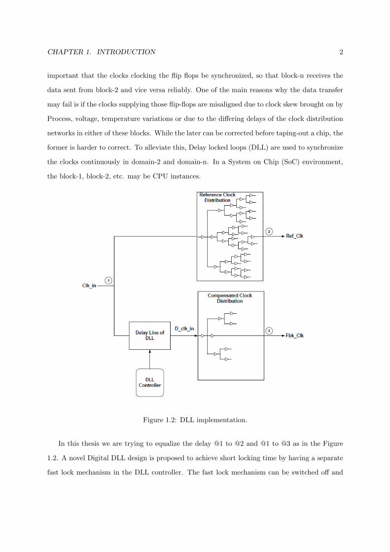
Figure 1.2: DLL implementation.
In this thesis we are trying to equalize the delay @1 to @2 and @1 to @3 as in the Figure
1.2. A novel Digital DLL design is proposed to achieve short locking time by having a separate
fast lock mechanism in the DLL controller. The fast lock mechanism can be switched off and

CHAPTER 1. INTRODUCTION 3
the normal power dissipation can be achieved after the DLL has locked. The proposed DLL
also has less jitter after lock and less residual, uncorrectable offset. The thesis is organized as
following; In Chapter 1 the need for the DLLs, their working principle and the types of DLLs is
given. In Chapter 2 detailed schematic analysis of a Digital DLL is given. The modified DLL
architecture of digital DLL is described in Chapter 3. Finally, the results are discussed in detail
and compared with the results of other DLLs in 4.
1.1 Delay Locked Loop Overview
The reduction of clock skew is one of the important problems in the VLSI design. DLLs are used
in VLSI circuits in order to decrease clock screw in the clock networks. DLL is a feedback system
that aligns the feedback clock to the reference clock. This is done by delaying the input feedback
clock after passing it through a delay line and controlling the delay using the control mechanism.
Once the input feedback clock is delayed, a phase detector (PD) compares the phases of the two
inputs. Based on PD output value, the delay is adjusted (increased or decreased) until the two
phases are aligned. A DLL is widely used as a timing circuit in many systems for the purpose
of clock generation [9], [10], signal synchronization [11], and others [12]. For example, a DLL is
able to provide multiple clock signals which are separated from each other by a well-controlled
phase shift (delay). This application of DLL is widely used in DDR memory circuits to align the
DQS strobe in the middle of the data eye DQ. When appropriate logic, such as edge combining
is used, a new clock signal which is of a different frequency can be generated by the DLL.
Such an application of a DLL has been reported in [13] for personal communication services
(PCS). Another application of a DLL is for the purpose of clock deskewing in synchronous data
transfer among communication chips. Reducing clock skew has become increasingly important
with larger die size and higher clock frequency. A DLL for this application requires fast lock
time and good phase alignment between the reference signal and the corrected output signal. A
DLL serving as a clock deskew buffer was reported in [14] and is also discussed in this thesis . In
addition, a DLL can also be used for signal synchronization, for example, between a CPU and
a co-processor so that they can share the same data bus. This application was reported in [15].

CHAPTER 1. INTRODUCTION 4
Many of the above applications share similar requirements for the DLL, such as a short locking
time, low jitter, and a wide locking range [2]. DLLs can be either primarily analog [14], [16] or
primarily digital [17], [18] depending on the design components. Both of these are discussed in
the next sections.
1.1.1 Analog DLL
Analog DLLs were first used in clock distribution applications [9], [16]. The components of a
conventional Analog DLL are, phase detector, charge pump, low pass filter and voltage con-
trolled delay line as shown in Figure 1.3.
Figure 1.3: Conventional Analog DLL.
A phase detector compares two input signals and generates ”UP” and ”DN” output pulses
that represent the direction and magnitude of the input phase error. There are many types of
phase detectors; they differ in how they sense the input signals, what input phase difference
would result to detect no phase error, and how the phase error is represented in the output
pulses. Considering simple type of phase detectors such as the phase-frequency detectors are
those which are only rising and falling edge sensitive. They produce a single pulse at the UP or
DN output for each pair of input reference and feedback edges depending on which edge arrives
first. A charge pump, connected to the phase detector, sources or sinks current for the duration
of the UP and DN pulses from the phase detector. The net output charge is proportional to the
difference between the pulse widths of the UP and Dn outputs. The charge pump drives the
loop filter which integrates and filters the charge current to produce the control voltage. The
control Voltage drives a voltage-controlled delay line (VCDL) in a DLL which generates a delay
proportional to the control voltage [19].

CHAPTER 1. INTRODUCTION 5
1.1.2 Digital DLL
Digital DLLs are characterized by their use of digitally controlled delay line. They are typically
made of simple digital circuit elements. Figure 1.4 shows a conventional Digital DLL. The
simplicity of the digital circuit elements helps to design portable digital DLL which can be
adapted to different technologies. The conventional digital DLLs provide only moderate phase
resolution, lock time and jitter performance [17], [18], [20], [21], [6], [22], [23], [24].
Figure 1.4: Conventional Digital DLL.
The control logic controlling the delay line has been implemented in different ways. An
example of the Digital DLL with one of the designs of control logics will be discussed in Chapter
2.
1.1.3 Comparison between Analog DLL and Digital DLL
An analog DLL is a complex analog circuit requiring process-specific implementation. Scaling
of analog integrated circuits directly affects output resistance and intrinsic gain of the circuit.
As we cross below the 100nm mark, the design of these analog circuits becomes quite exigent,
especially for low supply voltages around 1 V. This results in higher power consumption and
enhanced design complexity. [25]. So, it is not practical to reuse the same design for different
technology, making analog DLL a non-portable architecture. Analog DLL generally provides
better jitter performance at the expense of greater complexity [24]. Analog DLLs are more
susceptible to process variations and less immune from power-supply noise because of smaller
noise margins. In an analog DLL, if the low pass filter has less capacitor value then this will
result in more jitter and thus providing more variation in Voltage controlled delay line. If the
CHAPTER 1. INTRODUCTION 6
capacitor value is increased to achieve less jitter then the area of the DLL increases. While
the analog circuits may be adversely affected by scaling, digital circuits become increasingly
efficient by operating at higher speeds, consuming less power and occupying smaller area [25].
Although the Digital DLL has more Jitter than Analog DLL, its greater simplicity, portability,
lower power consumption, its ability to operate at lower voltages, smaller area, more noise
immunity, short lock time and synthesizable circuit makes it very attractive for clock alignment
applications [26], [27], [28].
1.2 Conclusion
In this chapter general information about DLL and the types of DLL is described. The ad-
vantages and disadvantages of the Analog and Digital DLL are also discussed. The common
requirements for the design of a DLL are short locking time, low jitter performance, less power
consumption, small area and less phase error after lock or minimum time of resolution.
In the next chapter, a detailed discussion of the design of a Digital DLL is given.

Chapter 2
Design of a Digital DLL
The Digital DLLs are characterized by the controller that is used to control the delay line.
Digital DLLs are roughly divided into four categories. The first one is the Register-Controlled
DLL. The locked time and the number of delay cells increase exponentially as the number
of control bits increases. The second category is the Counter-Controlled DLL [3], [17]. The
counter-based controller [3], [17] replaces the register-based one to reduce the hardware of the
controller. However, the locked time and the required delay cells of the counter-controlled DLL
are similar to those of the register-controlled DLL. The third category is the DLL using the
Successive Approximation Register-Controlled(SAR) scheme [29]. It can reduce the locked time
by using the binary search algorithm. The last category is the DLL using the Time-to-Digital
Converter (TDC) [30]. Large chip area and power are required especially when it operates in the
wide frequency range. Both TDC and SAR schemes are open-loop. The open-loop characteristic
is hard to track the process, voltage, temperature and loading (PVTL) variations. Besides, the
wide range DLLs usually needs an external reset signal when the frequency of input clock
changes significantly [28].
In this thesis, a Counter-Controlled DLL has been considered and the fast lock mechanism
has been added to the control logic to reduce the lock time of the DLL. Each component of the
conventional Counter-controlled digital DLL is discussed in detail in the following sections.
Digital DLL is composed of the following main component blocks.
• Phase detector (PD)
7

CHAPTER 2. DESIGN OF A DIGITAL DLL 8
• Control mechanism (CM)
• Digital controlled delay line (DCDL)
2.1 Phase Detector
In a digital DLL the output of the phase detector is a single signal (up/down) which drives
the subsequent counter or FSM depending upon the application of DLL. Generally a PD must
satisfy the following design requirements:
• To avoid false detection the PD should spend minimum time in metastable state.
• The setup and hold times must be reasonably small.
• The setup and hold times should be comparable so as the resulting phase information is not
biased.
• The clock to Q delay should be reasonably small but is usually not a stringent requirement.
Based on the different applications, different PDs have been proposed and implemented [31],
[2], [3]. Few types of PD designs are discussed here. The simplest of the phase detectors can be
a single D flip flop (DFF) as shown in Figure 2.1. The DFF is clocked by the input reference
clock and detects the difference between the clocks by selecting the Q output of the DFF. If the
Q output is low it means that the output clock (clock signal form the end of digitally controlled
delay line) is leading the input reference clock and thus the delay of the delay line must be
increased so as to compensate for the difference in phase until the lock condition is achieved [1].
Figure 2.1: D-flip flop based phase detector [1].

CHAPTER 2. DESIGN OF A DIGITAL DLL 9
Though this design is simple and effective, it has shortcomings. If the setup and hold times
are not symmetric this may introduce a regular phase error as lagging and leading decisions
based on the hold and setup times, respectively.
Figure 2.2: Dual output phase detector [2].
Figure 2.3: Dynamic phase detector [3].
Figure 2.2 shows another implementation of PD which doesn’t have the flaws of PD in Figure
2.1. This PD consists of two identical blocks generating UP or DOWN signal. Within each
block there are two stages with a pre-charge PMOS in each stage. Output of the first stage

CHAPTER 2. DESIGN OF A DIGITAL DLL 10
controls the second stage pre-charging.
Figure 2.3 shows another PD design. To align signal phases with precision, it is important
to reduce dead zones in the PDs. The dynamic PD in Figure 2.3 improves the phase sensitivity
of Latch 1 because sharper waveforms of the reference clock and the feedback clock are obtained
by using precharged dynamic circuits. Latch 2 is connected to Latch 1 to hold the signal states.
2.2 Control Mechanism
The controlling mechanism of the digital DLL also varies based on the application of the DLL.
Counter-Controlled DLLs could be implemented in two ways. Figure 2.4 and Figure 2.5 shows
these two implementations.
A straight forward control mechanism is shown in Figure 2.4. In this design, the PD controls
an up/down counter that is used to set the delay of the DCDL so as to compensate for the
phase difference between the PD inputs. When the output of the PD is high, the counter
is incremented, increasing the delay of DCDL and when PD output is low, the counter is
decremented, to decrease the delay of DCDL, thus attaining the lock condition [1].
Figure 2.4: Control mechanism in Digital DLLs [4].
The Figure 2.5 shows an advanced control mechanism in which a finite state machine (FSM)
is placed between the PD and the up/down counter. Here, the FSM sends a high or low signal
to the input of the counter not only based on the PD output but also on the internal state of
the FSM, which is set based on the initial conditions of the system. The design of such an FSM

CHAPTER 2. DESIGN OF A DIGITAL DLL 11
is very complex and may directly affect the dynamic range and stability of DLL [1].
Figure 2.5: Finite state machine based control block in Digital DLLs [4].
2.3 Digital Controlled Delay Line
The delay line is the most important component of the DLL and has a profound effect on the
overall performance of the DLL. Commonly, digital DLLs are composed of two delay lines:
a coarse delay line and a fine delay line. The coarse delay line is also referred to as Gate-
delay DCDLs while the fine delay line is also referred to as Subgate-delay DCDL. There are
various number of delay line structures that are employed or that have been proposed for
different applications. The following section briefly discusses few of the commonly used DCDL
structures.
2.3.1 Coarse Delay Line
The coarse delay lines are composed of CMOS logic gates and are cascaded to form a delay line.
The simplest of the delay lines for digital DLL is a chain of cascaded inverters with each stage
consisting of a pair of inverters and the required output tap is selected by a multiplexer. The
minimum delay of each stage is 2TD where TD is the average CMOS gate delay and requires
log2N storage elements where N is the number of stages [1]. A coarse delay line design discussed
in [4] is shown in the Figure 2.6 .
This implementation has four delay stages between the input and output. If the number
of delay stages is increased as per the design requirement, this may load the input clock. To

CHAPTER 2. DESIGN OF A DIGITAL DLL 12
overcome the loading, separate buffers must be introduced thus increasing the delay of each cell
to more than 2TD. This increase in delay would depend on the amount of added buffering [4], [1].
Figure 2.6: Inverter based digital controlled coarse delay line [4].
Figure 2.7: Nand based digital controlled coarse delay line [4].

CHAPTER 2. DESIGN OF A DIGITAL DLL 13
A work-around to this problem is shown in Figure 2.7. In this structure, the loading on
the input clock is prevented by varying the delay line in a telescopic fashion. Adapting this
structure eliminates the need to introduce internal buffering of the clock signal thus maintaining
the delay of each stage to 2TD. A shift register controls the delay of each cell of these cells. For
example, when Q [0] =1 and Q [3:1] =0 the output clock signal would have a two nand gate
delay i.e. the delay of A and B nand gates in cell 0. When Q [1] =1 and the rest of the values
are low the output path would be nand gate C in cell 0, nand gate A in cell 1, nand gate B in
cell 1, nand gate B in cell 0. The wrap around in the delay cell 3 toggles the delay line between
various modes [4], [1].
Figure 2.8 shows another implementation of coarse delay line. Here, the delay line consists
of multiple delay cells connected as shown in the Figure 2.8. Each delay cell consists of a
multiplexer (MUX) and a buffer. The input1 of the MUX of first delay cell is connected to vdd
and for all other delay cells the input1 is connected to the output of the previous stage cell.
The input2 of all the MUX are connected to clock. The delay line is controlled through the
select lines which are the output of the control logic.
Figure 2.8: MUX based digital controlled coarse delay line [5].
In this thesis, we are using similar MUX based digital controlled delay line.
2.3.2 Fine Delay Line
Two designs of the fine delay line, which generate delay by using the RC delay characteristics
are shown in Figure 2.9 and Figure 2.10. The structure in Figure 2.9 relies on varying cell
resistance. The branches are controlled by using digital bits Q [2:0] which switch in a fixed
specified pattern. The bits can only be thermometric ally encoded for this circuit due to poor

CHAPTER 2. DESIGN OF A DIGITAL DLL 14
linearity behavior of the circuit. For increased dynamic range several stages can be cascaded.
The greater the number of devices that are ON at a particular time smaller will be the RC
delay.
Figure 2.9: Typical digital controlled fine delay line [4].
In the second design of the fine delay shown in Figure 2.10, the RC delay increases with the
number of ON devices. The digital control bits can be encoded using both thermometric and
logarithmic codes due to linear characteristics of the circuit. As in former structure the dynamic
range increases by cascading several stages [1]. These RC based delay lines are discussed in more
detail in [4].
Figure 2.10: Thermometric/logarithmic digital controlled fine delay line [4].
The design proposed in [6] also helps to have very fine phase resolution which can be used
as the fine delay line. This design uses the inverter phase blending mechanism as shown in

CHAPTER 2. DESIGN OF A DIGITAL DLL 15
the Figure 2.11. This circuit receives two phase adjacent input signals, ΦA and ΦB, which are
separated in phase by one inverter delay. The phase blender directly passes these two signals
with a simple delay to produce output signals φA, φB and it also uses a pair of phase-blending
inverters to interpolate between these two input signals to produce a third output signal, φAB,
having a phase between that of φA and φB and this effectively doubles the available phase
resolution. The graph in Figure 2.11 shows the output phase blended waves. Phase blending
mechanism is discussed in detail in [6].
Figure 2.11: Phase blending circuit as the fine delay line and its output waveforms [6].
2.4 Conclusion
In this chapter detailed information about the Digital DLL and previous Digital DLL component
designs is provided. These designs forms the basis for the design of the DLL in this thesis.
In the next chapter detailed design of the proposed Digital DLL is given.

Chapter 3
Design of Proposed Fast Lock
Digital DLL
The proposed DLL is an improved design of a Counter-Controlled Digital DLL as mentioned
before. This chapter covers the block diagram of the proposed DLL along with the detailed
explanation of each module in the block diagram. The logic design is also described thoroughly.
The design goal is to reduce the lock time of the DLL without changing the power consumption
of the circuit after lock and also to reduce the jitter and the residual, uncorrectible offset DLL
with the DLL operating frequency of 280MHz - 1.63GHz.
Figure 3.1: Counter-controlled Digital DLL.
16

CHAPTER 3. DESIGN OF PROPOSED FAST LOCK DIGITAL DLL 17
The process used for the design and simulation of the proposed DLL is 45nm CMOS technol-
ogy. The tools used for the design and simulation are Cadence and HSPICE respectively. The
Figure 3.1 and Figure 3.2 shows the block diagram of a complete Digital DLL without the im-
plementation of the Fast lock mechanism and with the implementation of Fast lock mechanism
respectively.
Figure 3.2: Proposed Digital DLL.
3.1 Design Flow of the DLL controller
The complete design flow is given in this section. Figure 3.3 shows a flowchart of the design
flow of the proposed DLL. Once the start signal is asserted, the counters and the flip flops in
the DLL are reset. If the Up Dn output signal of the PD is high(1), then the 5-bit counter
increments. If the Up Dn signal is low(0), then the 5-bit counter decrements. Depending on the
amount of clock skew, the fast lock block in the fast lock mechanism provides the 8 bit control
word output to the encoder. The encoder converts the 8 bit control word to give 3-bit control
output to a set of flip flops. The 5-bit counter output and the clocked output from the encoder
flip-flop block are fed to the adder input. The adder adds these two inputs to give 5-bit sum
output. The buffered adder output is fed to a set of flops which helps to fix the adder output
after lock and also to select line and lock detect block.

CHAPTER 3. DESIGN OF PROPOSED FAST LOCK DIGITAL DLL 18
Figure 3.3: Proposed Digital DLL.
The output of the lock detector, Lock acts as the select line of the select block. If Lock is 1,
the select line selects the output of the flip flop block which will be fixed throughout the DLL
operation after lock. If Lock is 0, the select block selects the buffered adder output to feed the
input of the 5-to-32 bit decoder. The decoder generates the controller output to control the

CHAPTER 3. DESIGN OF PROPOSED FAST LOCK DIGITAL DLL 19
coarse delay line. Based on the controller output corresponding delay is added to the input
clock. Also, when Lock is 1, the 4 bit counter controlling the fine delay line is enabled and
when the Lock is 0, the 4 bit counter is disabled and the counter value is b’0000. This complete
process is repeated continuously in a loop as shown in the Figure 3.3 in order to align the
feedback clock (Fbk clk) to the reference clock (Ref clk) .
The proposed digital DLL also consists mainly of 3 parts namely,
• Phase detector (PD)
• Controller
• Digitally controlled delay line (DCDL)
The design of each block is discussed in detail in the following sections.
3.2 Phase Detector
The use of a PD and its different designs were discussed in chapter 2. The PD used in the
proposed DLL design is a dynamic PD. The block diagram showing the inputs and outputs of
the PD is shown in the Figure 3.4. Ref clk and Fbk clk are the inputs to the PD and Up dn is
the output signal. The PD consists of three SR latches and few basic gates connected as shown
in the Figure 3.5. The NOR gate is used to produce the reset signal for the PD. The first two
latches produce the PD output based on the clock skew between the Ref clk and the Fbk Clk.
The third latch is used to latch the PD output to the negative edge of the Ref clk. The dummy
is used for load balancing between the upper and lower part of the PD.
Figure 3.4: Block diagram of the Phase detector.

CHAPTER 3. DESIGN OF PROPOSED FAST LOCK DIGITAL DLL 20
Figure 3.5: Schematic of the Phase detector.
Figure 3.6: Input and output waveforms of the Phase detector.
The input and output waveforms of the PD are shown in the Figure 3.6. A, B and C in
Figure 3.6 shows the output of the PD for three different cases of the Fbk clk. A corresponds
to the output of PD when the Ref clk lags Fbk clk, B corresponds to the output when Ref clk
leads Fbk clk, and C refers to the output when the Ref clk and Fbk clk are exactly aligned.
CHAPTER 3. DESIGN OF PROPOSED FAST LOCK DIGITAL DLL 21
The PD output is high when the Ref clk lags Fbk clk. When the Ref clk leads Fbk clk, the
PD output goes low at the falling edge of the clock which appears first (here it is the Ref clk).
When the inputs are exactly aligned, the output of the PD goes high at the falling edge of
the clock appearing first. The PD is very sensitive and it can detect even 1ps of lead or lag
condition of the input clocks.
3.3 Controller
The controller block consists of different components namely,
• Binary up-down counters
• Fast lock mechanism
• Adder
• Lock detector
• Adder flip-flop block
• Select
• Decoder
Each of these components are discussed in detail in the following sections.
3.3.1 Binary Up-Down Counter
A binary Up-down counter is a counter which counts up when the input of the counter is high
and counts down when the input is low [32]. Two counters are used in the proposed DLL. They
are,
• 5-bit up-down counter
• 4-bit up-down counter
3.3.1.1 5-Bit Up-Down Counter
A basic block diagram of the 5-bit up down counter is shown in the Figure 3.7. Up dn signal
from the PD is the data input(In) to the counter. The counter is clocked by the Ref clk%2 (f2)

CHAPTER 3. DESIGN OF PROPOSED FAST LOCK DIGITAL DLL 22
Figure 3.7: Block diagram of 5-bit counter.
Table 3.1: State table for the 5-bit up-down counter using DFF.

CHAPTER 3. DESIGN OF PROPOSED FAST LOCK DIGITAL DLL 23
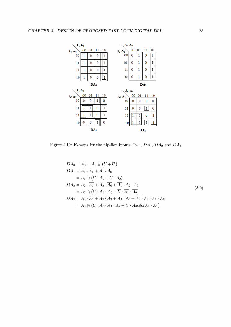
Figure 3.8: K-maps for the flip-flop inputs, a) DA0, b) DA1, c) DA2, d) DA3 and e) DA4.
DA0 = A0 = A0 ⊕(U + U
)DA1 = A1 ·A0 +A1 ·A0
= A1 ⊕(U ·A0 + U ·A0
)DA2 = A2 ·A1 +A2 ·A0 +A1 ·A2 ·A0
= A2 ⊕(U ·A1 ·A0 + U ·A1 ·A0
)DA3 = A3 ·A1 +A3 ·A2 +A3 ·A0 +A3 ·A2 ·A1 ·A0
= A3 ⊕(U ·A0 ·A1 ·A2 + U ·A0 ·A1 ·A2
)DA4 = A0 ·A1 ·A2 ·A3 ·A4 +
(A1 +A3 +A2 +A0
)·A4
= A4 ⊕(U ·A0 ·A1 ·A2 ·A3 + U ·A0 ·A1 ·A2 ·A3
)
(3.1)

CHAPTER 3. DESIGN OF PROPOSED FAST LOCK DIGITAL DLL 24
clock(Clk). The counter is enabled when enb = 0. The counter acts as an Up counter when
Up dn = 1 and it acts as a Down counter when Up dn = 0. The outputs of the counter are
denoted as A [4 :0] . A4 is the MSB and A0 is the LSB in the output of the counter.
In order to design such a 5-bit counter, a state change table is created as shown in Table
3.1. Here U represents UP and D represents Down. In our design if Up = 1 then D =0 and if
Up=0 then D=1. Therefore D can be represented as U .
K-maps are usually used to derive the flip-flop input equations. By using the Table 3.1,
K-map is drawn as shown in the Figure 3.8. The flip-flop equations in 3.1 are derived for DA0,
DA1, DA2, DA3 and DA4 from the K-map. The schematic for the 5-bit counter is based on
the above mentioned equations obtained from the K-map. The equations in 3.1 shows that
the counter design requires up to 5 input AND gates. As the basic gates with more than 3
inputs are less efficient, the counter is designed with a maximum of 3 input AND gates and the
equation requiring more than 3 inputs gates have be simplified in the design. The Figure 3.9
shows the schematic of the 5-bit- up-down counter. The Figure 3.10 shows the output of the
counter.
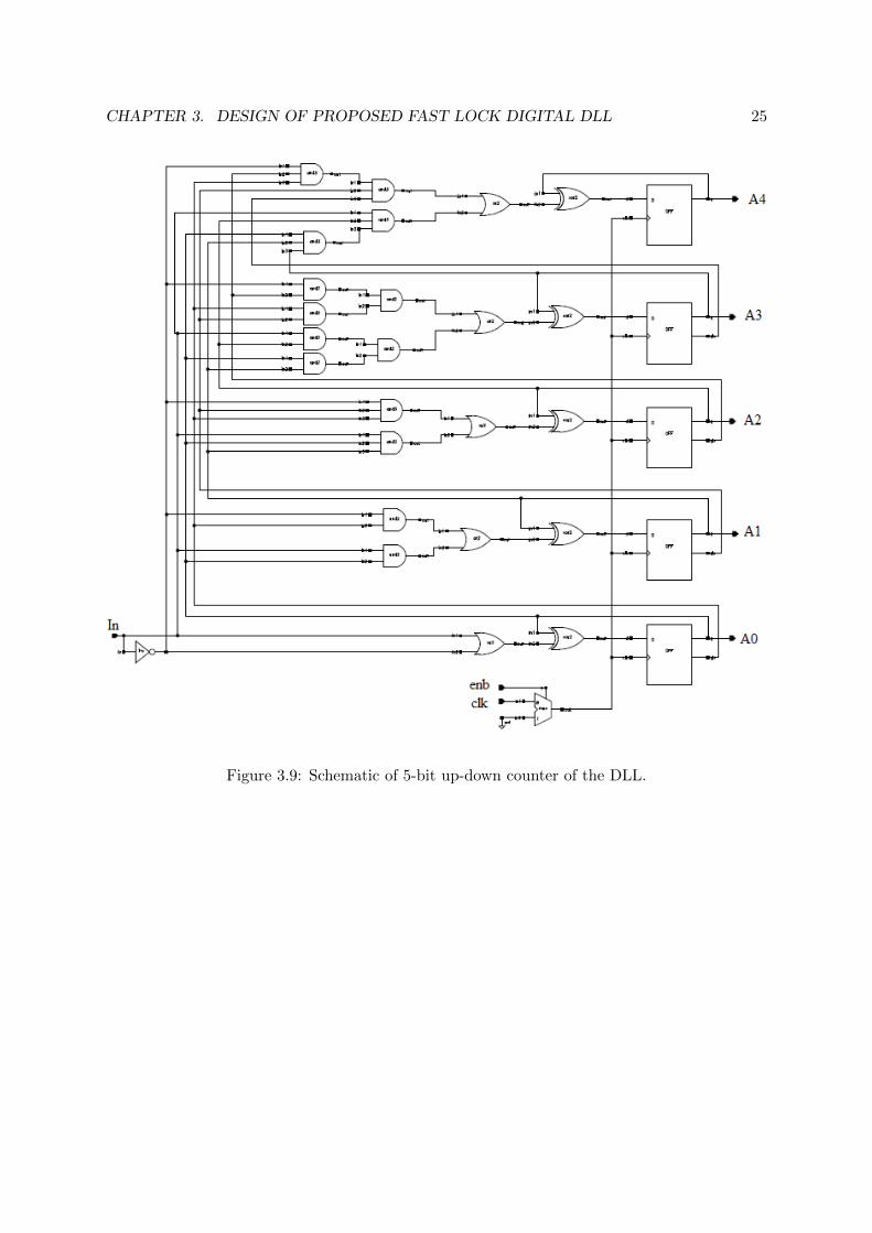
CHAPTER 3. DESIGN OF PROPOSED FAST LOCK DIGITAL DLL 25
Figure 3.9: Schematic of 5-bit up-down counter of the DLL.

CHAPTER 3. DESIGN OF PROPOSED FAST LOCK DIGITAL DLL 26
Figure 3.10: Output of 5-bit up-down counter.
3.3.1.2 4-Bit Up-Down Counter
The basic block diagram of the 4-bit up-down counter is shown in the Figure 3.11. As in the
5-bit counter, Up dn signal from the PD is the data input(In) to the counter. The counter is
clocked by the f2 clock (Clk) and it is enabled when en = 1. Even here, the counter acts as an
Up counter when Up dn = 1 and it acts as a Down counter when Up dn = 0. The outputs of
the counter are represented as A[3 :0]. A3 is the MSB and A0 is the LSB in the output of the
counter. In order to design such a 4-bit counter, a state change table is created as shown in
Table 3.2. In the table, U represents UP and D represents Down. In our design if Up = 1 then
D =0 and if Up=0 then D=1. Therefore D can be represented as U .

CHAPTER 3. DESIGN OF PROPOSED FAST LOCK DIGITAL DLL 27
Figure 3.11: Block diagram of 4-bit counter.
Table 3.2: State table for the 4-bit up-down counter using DFF.
K-maps are used to derive the flip-flop input equations as before. By using the Table 3.1,
K-map is drawn as shown in the Figure 3.12. From the K-maps, the equations 3.2 are derived for
DA0, DA1, DA2 and DA3.The schematic for the 4-bit counter is based on the above mentioned
equations obtained from the K-map. The equations in 3.2 shows that the counter design requires
up to 4 input AND gates. As mentioned in the 5-bit counter design, the counter is designed
with a maximum of 3 input AND gates and the equation requiring more than 3 inputs gates
have be simplified in the design. The Figure 3.13 shows the schematic of the 4-bit up-down
counter. The Figure 3.14 shows the output of the counter.
CHAPTER 3. DESIGN OF PROPOSED FAST LOCK DIGITAL DLL 28
Figure 3.12: K-maps for the flip-flop inputs DA0, DA1, DA2 and DA3
DA0 = A0 = A0 ⊕(U + U
)DA1 = A1 ·A0 +A1 ·A0
= A1 ⊕(U ·A0 + U ·A0
)DA2 = A2 ·A1 +A2 ·A0 +A1 ·A2 ·A0
= A2 ⊕(U ·A1 ·A0 + U ·A1 ·A0
)DA3 = A3 ·A1 +A3 ·A2 +A3 ·A0 +A3 ·A2 ·A1 ·A0
= A3 ⊕(U ·A0 ·A1 ·A2 + U ·A0cdotA1 ·A2
)(3.2)

CHAPTER 3. DESIGN OF PROPOSED FAST LOCK DIGITAL DLL 29
Figure 3.13: Schematic of 4-bit up-down counter of the DLL.

CHAPTER 3. DESIGN OF PROPOSED FAST LOCK DIGITAL DLL 30
Figure 3.14: Output of 4-bit up-down counter.
This 4-bit counter is used to control the Fine delay line, which will be discussed in Delay
Line section.
3.3.2 Fast Lock Mechanism
The addition of the fast lock mechanism to the conventional digital DLL design is the highlight
of this thesis. Figure 3.15 show its block diagram and it consists of three components namely,
• Fast lock block (FLB)
• Encoder
• Encoder flip-flops (EFF)

CHAPTER 3. DESIGN OF PROPOSED FAST LOCK DIGITAL DLL 31
Figure 3.15: Block diagram of Fast Lock Mechanism.
3.3.2.1 Fast Lock Block
The fast lock block is the main unit of the FLM. It consists of phase width detector(PWD), 8
MUXs denoted as fast lock block MUX (FLBM), DFF, buffers, transmission gate based 2-bit
MUXs and basic OR gate cascaded as shown in the Figure 3.16. The input to the FLB are the
Ref clk, Fbk clk, control inputs t[2:0], enb and reset. The outputs of FLBMs, first set of DFFs
and second set of DFFs(output of FLB) are denoted by CW[1:8], D[1:8] and C[1:8] respectively.
The FLB is enabled using enb as the select line of transmission gate MUXs which have the
inputs as Ref clk and Fbk clk. When enb = 1, the FLB is disabled as the Ref clk and Fbk clk
are not allowed to pass through the transmission gate MUXs and instead low signals are passed
through the circuit. When enb = 0 the FLB is enabled and the PWD detects the amount of
phase difference between the two clock signals. The Figure 3.17 shows the schematic of the
PWD. The buffered output of PWD acts as the select line of FLBMs. Each FLBM consists of
a MUX and few basic gates and NMOS transistors connected as shown in the Figure 3.18. The
3 transmission gates connected to 3 NMOS transistor help in providing different delay based
on the control inputs, t[2:0]. So, t[2:0] can be adjusted accordingly for different input clock
frequencies.

CHAPTER 3. DESIGN OF PROPOSED FAST LOCK DIGITAL DLL 32
Figure 3.16: Fast Lock Block.
Figure 3.17: Fast Lock Block.
The output of one FLBM is fed to the input of the next FLBM and also to the input of the
DFF. The width of the pulse at the output of FLBM gradually decreases from first FLBM to
last FLBM and depending on the phase difference between the input clocks, the pulse gradually
disappears. The amount of decrease in the width of the pulse at successive FLBM is equal

CHAPTER 3. DESIGN OF PROPOSED FAST LOCK DIGITAL DLL 33
to the delay of FLBM. The first DFF is used to detect the pulse at the output of FLBMs.
As the pulse widths could be very small, a DFF which has very less set-up and hold- time is
required. Hence the DFF design discussed in [7] is used. The schematic of the DFF is as shown
in the Figure 3.19. The set-up time and hold-time of the DFF is measured as 1ps and -14ps
respectively. The clock to Q delay of the DFF is measured as 75ps.
Figure 3.18: Fine Delay Unit.
Figure 3.19: D-Flip Flop [7].
The first DFF is clocked by the buffered output of the FLBM and is reset using delayed
Ref clk so as to ensure successful transmission of the data input to the output of the DFF.
The second DFF is used to latch the output of first DFF to the rising edge of the Ref clk. For

CHAPTER 3. DESIGN OF PROPOSED FAST LOCK DIGITAL DLL 34
example, when the phase difference between the Ref clk and the Fbk clk is 200ps, the outputs
at the FLBMs, first set of DFFs and second set of DFFs (output of FLB) are as shown in
Figure 3.20, Figure 3.21 and Figure 3.22 respectively. The 4 output lines of the FLB, C[1:4]
are high for a phase difference of 200ps. The Figure 3.23 shows different phase differences and
their corresponding active FLBM.
Figure 3.20: Output of FLBM for a phase difference of 200ps.

CHAPTER 3. DESIGN OF PROPOSED FAST LOCK DIGITAL DLL 35
Figure 3.21: Output of first set of DFFs for a phase difference of 200ps.

CHAPTER 3. DESIGN OF PROPOSED FAST LOCK DIGITAL DLL 36
Figure 3.22: Output of second set of DFFs for a phase difference of 200ps.

CHAPTER 3. DESIGN OF PROPOSED FAST LOCK DIGITAL DLL 37
Figure 3.23: Graph of phase difference Vs active FLBM.
3.3.2.2 Encoder
An encoder is a digital circuit which has 2n input lines and n output lines. An encoder that
generates a code based on the highest priority input is called a priority encoder [32].
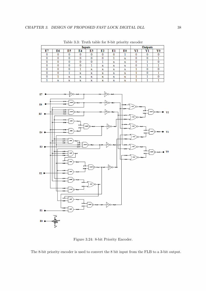
In this DLL, a 8-bit priority encoder is used as shown in the Figure 3.24. This circuit
basically converts a one-hot encoding into a binary representation. If input n is active, all lower
inputs (n-1 to 0) are ignored. Table 3.3 shows the truth table of the 8-bit priority encoder. The
encoder is designed based on the Boolean equations 3.3 obtained from the truth table in Table
3.3. The x term in the truth denotes don’t care terms which are ignored. In this DLL, the value
of x is always 1.
Y 2 = E7 + E6 + E5 + E4
Y 1 = E7 + E6 + E5 · E4 · E3 + E5 · E4 · E2
Y 0 = E7 + E6 · E5 + E6 · E4 · E3 + E6 · E4 · E2 · E1
(3.3)
CHAPTER 3. DESIGN OF PROPOSED FAST LOCK DIGITAL DLL 38
Table 3.3: Truth table for 8-bit priority encoder
Figure 3.24: 8-bit Priority Encoder.
The 8-bit priority encoder is used to convert the 8 bit input from the FLB to a 3-bit output.

CHAPTER 3. DESIGN OF PROPOSED FAST LOCK DIGITAL DLL 39
3.3.2.3 Encoder Flip-Flop
The encoder flip-flop (EFF) block has a set of flip flops to clock the 3-bit inputs to the rising
edge of the Ref clk. Figure 3.15 shows the block diagram of EFF as well. The input to the EFF
block are the outputs from the 8-bit encoder, Ref clk, Reset and en. The en signal is used to
fix the value of the encoder output after one Ref clk cycle. Thus, the EFF block output doesn’t
change in the successive clock cycles.
3.3.3 Adder
An adder is a digital circuit that performs addition of numbers. The most common adders
operate on binary numbers. A 5-bit Ripple carry adder is used in the DLL to add the 5-bit
counter outputs and the flopped 8-bit encoder outputs. Figure 3.25 shows the block diagram of
the adder.
Figure 3.25: Block diagram of Adder.
Ripple carry adder is designed using multiple full adders to add N-bit numbers. Each full
adder inputs a Cin, which is the Cout of the previous adder. This kind of adder is called a ripple
carry adder, since each carry bit ”ripples” to the next full adder [32]. A full adder (FA) is a
logical circuit that accepts two operand bits, say A and B, and an incoming carry bit, denoted by
Cin to give output Sum and an outgoing carry bit denoted by Cout. The FA is a combinational
digital circuit implementing the binary addition of three bits through the Boolean equations in
3.4. Ripple carry adder is preferred in our design due to its less complexity and area efficiency.

CHAPTER 3. DESIGN OF PROPOSED FAST LOCK DIGITAL DLL 40
Sum = A⊕B ⊕ Cin
Cout = A ·B + (A+B) · Cin(3.4)
Figure 3.26: a) 5-bit Ripple Carry Adder b) Full Adder.
However, the delay time for worst case is more when compared to other adders. Figure 3.26
shows a 5-bit ripple carry adder and a full adder. Here, inputs A[4:0] are the 5-bit counter
outputs and B[2:0] are the flopped encoder outputs. B3, B4, Cin and Cout are connected to
ground. S[4:0] represents the adder sum outputs SUM[4:0].
3.3.4 Lock Detector
The lock detector(LD) plays a very important role in the functioning of the DLL. LD is used
to check the dithering condition of the adder output as shown in Figure 3.27. The schematic
representation of the LD is shown in Figure 3.28. It consists of a pair of DFFs connected in
series for each bit of the adder output. The inputs of the LD are the buffered outputs of the

CHAPTER 3. DESIGN OF PROPOSED FAST LOCK DIGITAL DLL 41
Figure 3.27: Graphs showing the dithering condition in DLL.
Figure 3.28: Lock Detector.
adder denoted by S[4:0], f2 and reset signal and the output is the lock signal. Each bit of
the buffered adder output is compared with the corresponding second DFF output to check if
they are same by using the basic XNOR gate. When all the output bits of the adder are same
for 2 consecutive cycles, then the output of all the XNOR gates will be high and at this point

CHAPTER 3. DESIGN OF PROPOSED FAST LOCK DIGITAL DLL 42
the lock signal goes high and the DLL is considered to be locked. Once the DLL is locked, the
lock signal is tied high for all the successive cycles of the DLL using the DFF at the output of
the AND gate as shown in the Figure 3.28. The lock signal is used to control different blocks of
the DLL namely, adder flip-flop block, select block, 4-bit counter and also the fast lock block.
The role of the lock signal in these blocks is discussed in the corresponding sections.
3.3.5 Adder Flip-Flop block
The set of flip-flops used to flop the buffered adder outputs is the Adder flip-flop(AFF) block.
Figure 3.29 shows the block diagram of AFF. The inputs to the AFF are S[4:0] from the adder,
lock, reset and Ref clk (clk). The output of AFF is denoted by SF[4:0]. The lock signal from
the LD is used to fix the output of adder to a particular value. When lock = 0, the output of
AFF is same as the output of adder and when lock =1, the output of AFF will be fixed to the
previous adder output and does not change in the successive clock cycles.
Figure 3.29: Block diagram of Adder Flip-Flop block.
3.3.6 Select
The select block consists of a set of transmission gate based MUXs to choose between the
buffered adder output and the flopped adder output. Figure 3.30 shows the block diagram of
the select block. The inputs S[4:0] and SF[4:0] denote the adder output and the AFF output
respectively and SM[4:0] denotes the select block output. The output of LD acts as the select
line of the MUXs in the select block. When lock = 1, the AFF output is selected and when

CHAPTER 3. DESIGN OF PROPOSED FAST LOCK DIGITAL DLL 43
lock = 0, the buffered adder output is selected by the select block.
Figure 3.30: Block diagram of Select.
3.3.7 Decoder
A decoder is a combinational circuit that converts binary information from n input lines to a
maximum of 2n unique output lines [33]. A 5-to-32 bit decoder is used in the DLL. This decoder
is used to convert the select block output to the control inputs of the coarse delay line. In this
thesis, the 5-to-32 decoder is obtained by using one 2-to-4 decoder and four 3-to-8 decoder as
shown in the Figure 3.31.
A 2-to-4 decoder has 2 input lines and 22 = 4 output lines as shown in Figure 3.32. The
2-to-4 decoder is implemented through Boolean equations in 3.5. This decoder controls the
enable input of the four 3-to-8 decoders in the 5-to-32 decoder as in Figure 3.31.

CHAPTER 3. DESIGN OF PROPOSED FAST LOCK DIGITAL DLL 44
Figure 3.31: 5-to-32 Decoder.
Figure 3.32: 2-to-4 Decoder.

CHAPTER 3. DESIGN OF PROPOSED FAST LOCK DIGITAL DLL 45
D0 = I1 · I0 · EnD1 = I1 · I0 · EnD2 = I1 · I0 · EnD3 = I1 · I0 · En
(3.5)
Similarly, a 3-to-8 decoder has 3 input lines and 23 = 8 output lines as shown in Figure 3.33
and it is implemented through the Boolean equations in 3.6.
Figure 3.33: 3-to-8 Decoder.
D0 = I2 · I1 · I0 · EnD1 = I2 · I1 · I0 · EnD2 = I2 · I1 · I0 · EnD3 = I2 · I1 · I0 · EnD4 = I2 · I1 · I0 · EnD5 = I2 · I1 · I0 · EnD6 = I2 · I1 · I0 · EnD7 = I2 · I1 · I0 · En
(3.6)

CHAPTER 3. DESIGN OF PROPOSED FAST LOCK DIGITAL DLL 46
3.4 Digital Controlled Delay Line
The delay line consists of two components namely,
• Coarse delay line
• Fine delay line
3.4.1 Coarse Delay Line
A MUX based coarse delay line(CDL) is used in this DLL. The CDL consists of 32 coarse delay
units(CDU) as shown in the Figure 3.34. The design of CDU is same as that of the FLBM
as shown in Figure 3.35. Each CDU has a 2-to-1 MUX and few basic gates as shown in the
Figure 3.35. The output from the MUX in the previous stage is fed to the input 1 of the
MUX and the clock is fed to the input 2 of all the MUXs. The 32 bit control signal from the
5-to-32 bit decoder serves as the select lines of the MUXs in the CDL. The 3 transmission gates
connected to 3 NMOS help in providing different delay based on the control inputs, t[2:0]. Each
CDU provide a delay between 32ps - 46ps depending on the control inputs. This helps to have
DLL operate for a wide range of frequencies between 280MHz to 1.62GHz. Table 3.4 gives the
different control inputs and the corresponding delay of each CDU. The output of the CDL is
the delayed clock and the amount of delay is based on the controller outputs.
Figure 3.34: Coarse Delay Line

CHAPTER 3. DESIGN OF PROPOSED FAST LOCK DIGITAL DLL 47
Figure 3.35: Coarse Delay Unit.
Table 3.4: Control inputs T[2:0] and the corresponding delay of CDU.
3.4.2 Fine Delay Line
The fine delay line(FDL) mainly consists of two components namely,
• Fine delay block
• 16-bit Multiplexer
The output of the CDL is the input to the FDL. Figure 3.36 shows the block diagram of
the FDL.

CHAPTER 3. DESIGN OF PROPOSED FAST LOCK DIGITAL DLL 48
Figure 3.36: Fine Delay Line.
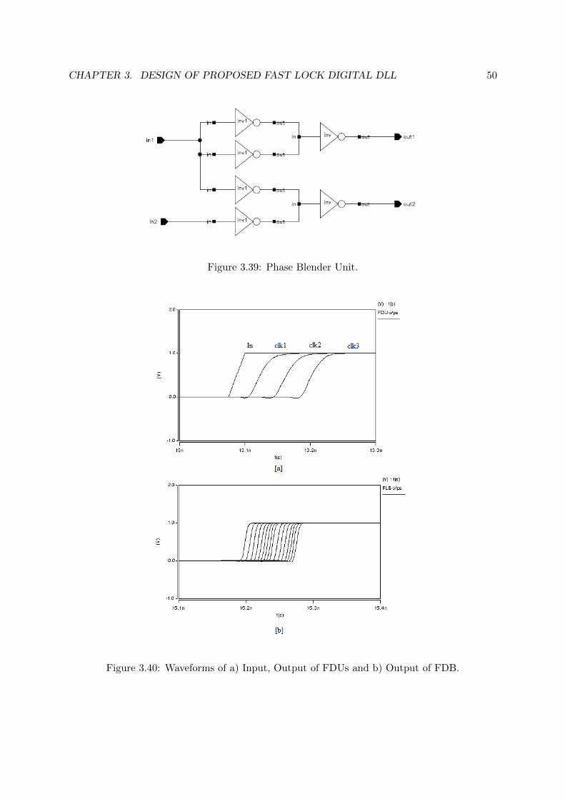
3.4.2.1 Fine Delay Block
The design of the fine delay block(FDB) is mainly based on the phase blending technique
discussed in [6]. The phase blending was explained in chapter 2 as well. FDB consists of 3
fine delay units (FDU), multiple phase blenders and dummy blocks as shown in the Figure
3.37. The design of FDU is same as that of the FLBM shown in Figure 3.38. FDUs are used
to generate clock signals of three different phases from a single clock input. The FDUs are
cascaded in such a way that the output of first FDU is fed to a input of the second FDU and
the output of second FDU is in turn fed to the input of the third FDU. The output of the
FDUs, clk1, clk2 and clk3 are blended in three stages so as to get 16 signals, c1 to c16 which
are of different phases. Figure 3.39 shows the circuit of a phase blender unit. The minimum
phase difference between any two consecutive outputs of the FDB is 4ps. So, the minimum
time resolution or the residual, uncorrectible offset of the DLL is 4ps. The outputs of the three
FDUs and the 16 phase blended outputs of the FDB are shown in Figure 3.40. As explained
in the CDL section, the control bits t[2:0] helps in adjusting the delay of the FDU according
to the frequency of operation of the DLL. The advantage of having FDU based FDL is, as the
delay of the FDU changes, the phase difference between the consecutive outputs of the FLB
also changes proportionately. This helps in having the FDL work in accordance with the CDL.

CHAPTER 3. DESIGN OF PROPOSED FAST LOCK DIGITAL DLL 49
Figure 3.37: Fine Delay Block.
Figure 3.38: Fine Delay Unit.
CHAPTER 3. DESIGN OF PROPOSED FAST LOCK DIGITAL DLL 50
Figure 3.39: Phase Blender Unit.
Figure 3.40: Waveforms of a) Input, Output of FDUs and b) Output of FDB.

CHAPTER 3. DESIGN OF PROPOSED FAST LOCK DIGITAL DLL 51
3.4.2.2 16-bit Multiplexer
A n-bit multiplexer takes n input signals, and shifts one of them to the single output under the
control of log2n bit select signal [33]. A 16-bit MUX has 16 input signals with 4 select lines and
a single output as shown in Figure 3.41. This 16-bit MUX is designed using two 8-bit MUXs
and one 2-bit MUX. The output of the 4-bit up-down counter discussed in the controller section
acts as the 4-bit select line of the 16-bit MUX.
Figure 3.41: 16-bit Multiplexer.
Each 8-bit MUX consists of multiple 2-bit MUXs connected as shown in the Figure 3.42.
The 2-bit mux used in this design are simple transmission gate MUXs with very less delay. The
Figure 3.42 also shows the path from input to output for the select line input, S[2:0]= b’100.

CHAPTER 3. DESIGN OF PROPOSED FAST LOCK DIGITAL DLL 52
Figure 3.42: 8-bit Multiplexer showing input to output path for S[2:0] = b’100.
3.5 Conclusion
In this chapter, detailed information about the design of each block of the proposed Digital
DLL and their corresponding simulation results are given. The advantage and the purpose of
using a particular design for each block is also explained.
In the next chapter, the results of the complete DLL are discussed and also the results of
the proposed DLL are compared with the results of other analog and digital DLLs..

Chapter 4
Results and Performance Analysis
The total number of NMOS and PMOS transistors used in the proposed DLL design are 2011
and 2403 respectively. The number of lock cycles, jitter after lock, power dissipation, and phase
error are the most important parameters considered for the performance analysis of the DLL.
The Monte-carlo simulation is carried out for a Monte Value of 30 with the following variations
in order to obtain the jitter values.
• Voltage variation from 0.9V to 1.1V with a step of 0.02
• Temperature variation from 25F to 125F with a step of 25F
• Gaussian distribution for channel length with Mean= 50nm, Absolute variation = ±2 and
σ = 3
The detailed performance analysis for two cases of phase differences between the Ref clk
and Fbk clk is given.
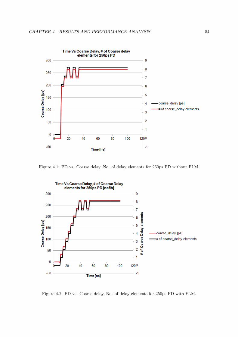
• Case1: Phase Difference = 200ps
In order to align the Fbk clk to Ref clk with different phase differences, the number of lock
cycles utilized by the DLL with and without fast locking mechanism is plotted in the Figure 4.2
and Figure 4.1 respectively. The Figure 4.2 and Figure 4.1 shows that less number of cycles are
required to align the Fbk clk to ref clk when compared to that of the DLL without FLM. The
RMS jitter and peak to peak jitter values are measured as 1.084ps and 2.169ps respectively as
shown in Figure 4.3
53
CHAPTER 4. RESULTS AND PERFORMANCE ANALYSIS 54
Figure 4.1: PD vs. Coarse delay, No. of delay elements for 250ps PD without FLM.
Figure 4.2: PD vs. Coarse delay, No. of delay elements for 250ps PD with FLM.

CHAPTER 4. RESULTS AND PERFORMANCE ANALYSIS 55
Figure 4.3: Jitter values for 250ps PD.
• Case2: Phase Difference = 500ps
In order to align the Fbk clk to Ref clk with different phase differences, the number of lock
cycles utilized by the DLL with and without fast locking mechanism is plotted in the Figure 4.5
and Figure 4.4 respectively. The Figure 4.2 and Figure 4.1 also shows that less number of cycles
are required to align the fbk clk to ref clk when compared to that of the DLL without FLM.
The RMS jitter and peak to peak jitter values are measured as 5.26ps and 10.57ps respectively
as shown in Figure 4.6

CHAPTER 4. RESULTS AND PERFORMANCE ANALYSIS 56
Figure 4.4: PD vs. Coarse delay, No. of delay elements for 500ps PD without FLM.
Figure 4.5: PD vs. Coarse delay, No. of delay elements for 500ps PD with FLM.

CHAPTER 4. RESULTS AND PERFORMANCE ANALYSIS 57
Figure 4.6: Jitter values for 500ps PD.
The Figure 4.7 shows the graph of PD vs. lock and it is plotted using the values in Table 4.1.
The graph shows that the lock time is less for the DLL with fast lock mechanism when compared
to that of a conventional DLL. Figure 4.8 shows the graph of PD vs. power consumption before
and after DLL locks. The graph shows that the power consumption of the DLL after lock
is almost same as that of the power consumption of the conventional DLL as the fast lock
mechanism is turned off after DLL locks.

CHAPTER 4. RESULTS AND PERFORMANCE ANALYSIS 58
Figure 4.7: PD vs. Lock cycles for proposed DLL.
Table 4.1: PD and corresponding lock cycle values of the proposed DLL.

CHAPTER 4. RESULTS AND PERFORMANCE ANALYSIS 59
Figure 4.8: PD vs. Power consumption before and after lock for proposed DLL.
The Table 4.2 shows the performance comparison of the proposed DLL with other analog
DLLs in [10], [34] and [35]. From this we can infer that the jitter values of the proposed DLL
are on par with that of the analog DLLs.
Table 4.2: Performance comparison of the proposed DLL with other Analog DLLs.
The Table 4.2 shows the performance comparison of the proposed DLL with other digital
DLLs in [36], [ [37], [38], [39], [40] and [41]. This shows that the performance of the proposed
DLL is better than that of the DLLs discussed in [36], [ [37], [38], [39], [40] and [41].

CHAPTER 4. RESULTS AND PERFORMANCE ANALYSIS 60
Table 4.3: Performance comparison of the proposed DLL with other Digital DLLs.
Chapter 5
Conclusion and Future Works
DLL plays a vital role in the successful error free data transfer between different clock domains
by aligning clocks of different domains to the reference clock. The proposed DLL has improved
performance in terms of lock cycles, jitter and less residual, uncorrectable offset by bringing
back the power consumption of the DLL to normal values after lock. The FLB of the proposed
DLL can detect a phase difference up to 400ps in a single cycle. After one cycle the FLB is
turned off. So, the delay line adjusts up to 400ps in a single cycle. For the phase difference
above 400ps, the delay line provides one delay unit delay for the successive clock cycles after the
first cycle. So, in order to further reduce the lock cycles and jitter, this design can be further
improved to store the value of the encoder output in the first cycle and then add the encoder
output values obtained in each cycle to the stored value successively.
61

Bibliography
[1] Y. A. Shah and M. T. Pasha, “A wide range low power low jitter all digital dll for videoapplications,” p. 86, 2010.
[2] C. Jia, “A delay-locked loop for multiple clock phases/delays generation,” http://smartech.gatech.edu/handle/1853/7470.
[3] K. Minami, M. Mizuno, H. Yamaguchi, T. Nakano, Y. Matsushima, Y. Sumi, T. Sato,H. Yamashida, and M. Yamashina, “A 1 ghz portable digital delay-locked loop with infi-nite phase capture ranges,” in Solid-State Circuits Conference, 2000. Digest of TechnicalPapers. ISSCC. 2000 IEEE International, 2000, pp. 350 –351, 469.
[4] T. Xanthopoulos, Clocking in Modern VLSI Systems, ser. Integrated Circuits and Systems.Springer, 2009. [Online]. Available: http://books.google.com/books?id=pG11yIbLmJoC.
[5] Y.-M. Wang and J.-S. Wang, “A low-power half-delay-line fast skew-compensation circuit,”Solid-State Circuits, IEEE Journal of, vol. 39, no. 6, pp. 906 – 918, june 2004.
[6] B. Garlepp, K. Donnelly, J. Kim, P. Chau, J. Zerbe, C. Huang, C. Tran, C. Portmann,D. Stark, Y.-F. Chan, T. Lee, and M. Horowitz, “A portable digital dll for high-speed cmosinterface circuits,” Solid-State Circuits, IEEE Journal of, vol. 34, no. 5, pp. 632 –644, may1999.
[7] A. Strollo, D. De Caro, E. Napoli, and N. Petra, “A novel high-speed sense-amplifier-basedflip-flop,” Very Large Scale Integration (VLSI) Systems, IEEE Transactions on, vol. 13,no. 11, pp. 1266 –1274, nov. 2005.
[8] S. Rusu and S. Tam, “Clock generation and distribution for the first ia-64 microproces-sor,” in Solid-State Circuits Conference, Digest of Technical Papers. ISSCC. 2000 IEEEInternational, 2000, pp. 176 –177.
[9] T. Kim and B. Kim, “Phase interpolator using delay locked loop [multiphase clock gener-ation],” in Mixed-Signal Design, Southwest Symposium on, feb. 2003, pp. 76 – 80.
[10] R. Farjad-Rad, W. Dally, H.-T. Ng, R. Senthinathan, M.-J. Lee, R. Rathi, and J. Poul-ton, “A low-power multiplying dll for low-jitter multigigahertz clock generation in highlyintegrated digital chips,” Solid-State Circuits, IEEE Journal of, vol. 37, no. 12, pp. 1804 –1812, dec. 2002.
[11] R. Aguiar and D. Santos, “Wide-area clock distribution using controlled delay lines,” inElectronics, Circuits and Systems, IEEE International Conference on, vol. 2, 1998, pp. 63–66.
62

BIBLIOGRAPHY 63
[12] H. Lee, H. Q. Nguyen, and D. Potter, “Design self-synchronized clock distribution networksin an soc asic using dll with remote clock feedback,” in ASIC/SOC Conference, 13th AnnualIEEE International, 2000, pp. 248 –252.
[13] G. Chien and P. Gray, “A 900-mhz local oscillator using a dll-based frequency multipliertechnique for pcs applications,” Solid-State Circuits, IEEE Journal of, vol. 35, no. 12, pp.1996 –1999, dec. 2000.
[14] S.-I. Liu, J.-H. Lee, and H.-W. Tsao, “Low-power clock-deskew buffer for high-speed digitalcircuits,” Solid-State Circuits, IEEE Journal of, vol. 34, no. 4, pp. 554 –558, apr. 1999.
[15] M. Johnson and E. Hudson, “A variable delay line pll for cpu-coprocessor synchronization,”Solid-State Circuits, IEEE Journal of, vol. 23, no. 5, pp. 1218 –1223, oct. 1988.
[16] H.-H. Chang, C.-H. Sun, and S.-I. Liu, “A low-jitter and precise multiphase delay-lockedloop using shifted averaging vcdl,” in Solid-State Circuits Conference, 2003. Digest ofTechnical Papers. ISSCC. 2003 IEEE International, 2003, pp. 434 – 505 vol. 1.
[17] T. Hamamoto, K. Furutani, T. Kubo, S. Kawasaki, H. Iga, T. Kono, Y. Konishi, andT. Yoshihara, “A 667-mb/s operating digital dll architecture for 512-mb ddr sdram,” Solid-State Circuits, IEEE Journal of, vol. 39, no. 1, pp. 194 – 206, jan. 2004.
[18] T. Matano, Y. Takai, T. Takahashi, Y. Sakito, I. Fujii, Y. Takaishi, H. Fujisawa,S. Kubouchi, S. Narui, K. Arai, M. Morino, M. Nakamura, S. Miyatake, T. Sekiguchi,and K. Koyama, “A 1-gb/s/pin 512-mb ddrii sdram using a digital dll and a slew-rate-controlled output buffer,” Solid-State Circuits, IEEE Journal of, vol. 38, no. 5, pp. 762 –768, may 2003.
[19] A. Chandrakasan, F. Fox, W. Bowhill, and W. Bowhill, Design of high-performancemicroprocessor circuits. IEEE Press, 2001. [Online]. Available: http://books.google.com/books?id=EZoeAQAAIAAJ.
[20] J.-B. Lee, K.-H. Kim, C. Yoo, S. Lee, O.-G. Na, C.-Y. Lee, H.-Y. Song, J.-S. Lee, Z.-H. Lee,K.-W. Yeom, H.-J. Chung, I.-W. Seo, M.-S. Chae, Y.-H. Choi, and S.-I. Cho, “Digitally-controlled dll and i/o circuits for 500 mb/s/pin times;16 ddr sdram,” in Solid-State CircuitsConference, 2001. Digest of Technical Papers. ISSCC. 2001 IEEE International, 2001, pp.68 –69, 431.
[21] S. Eto, H. Akita, K. Isobe, K. Tsuchida, H. Toda, and T. Seki, “A 333 mhz, 20 mw, 18ps resolution digital dll using current-controlled delay with parallel variable resistor dac(pvr-dac),” in ASICs, 2000. AP-ASIC 2000. Proceedings of the Second IEEE Asia PacificConference on, 2000, pp. 349 –350.
[22] B.-S. Kim and L.-S. Kim, “100 mhz all-digital delay-locked loop for low power application,”Electronics Letters, vol. 34, no. 18, pp. 1739 –1740, sep. 1998.
[23] ——, “A low power 100 mhz all digital delay-locked loop,” in Circuits and Systems, 1997.ISCAS ’97., Proceedings of 1997 IEEE International Symposium on, vol. 3, june 1997, pp.1820 –1823.

BIBLIOGRAPHY 64
[24] A. Saghafi, “A novel high resolution Delay Locked loop,” https://circle.ubc.ca/handle/2429/16709.
[25] S. Henzler, Time-to-Digital Converters, ser. Springer Series in Advanced Microelectronics.Springer, 2010. [Online]. Available: http://books.google.com/books?id=L2H0FTxheH4C.
[26] T. Liran and R. Ginosar, “All-digital dll architecture and applications,”http://webee.technion.ac.il/∼ran/papers/All-Digital%20DLL%20Architecture%20and%20Applications.pdf, 2008.
[27] D. Shin, J. Song, H. Chae, K.-W. Kim, Y. J. Choi, and C. Kim, “A 7ps-jitter 0.053mm2fast-lock addll with wide-range and high-resolution all-digital dcc,” in Solid-State CircuitsConference, 2007. ISSCC 2007. Digest of Technical Papers. IEEE International, feb. 2007,pp. 184 –595.
[28] S.-K. Kao, B.-J. Chen, and S.-I. Liu, “A 62.5-625-mhz anti-reset all-digital delay-lockedloop,” Circuits and Systems II: Express Briefs, IEEE Transactions on, vol. 54, no. 7, pp.566 –570, july 2007.
[29] G.-K. Dehng, J.-M. Hsu, C.-Y. Yang, and S.-I. Liu, “Clock-deskew buffer using a sar-controlled delay-locked loop,” Solid-State Circuits, IEEE Journal of, vol. 35, no. 8, pp.1128 –1136, aug. 2000.
[30] S.-K. Kao and S.-I. Liu, “All-digital clock deskew buffer with variable duty cycles.” IEICETransactions, pp. 753–760, 2006.
[31] S. Soliman, F. Yuan, and K. Raahemifar, “An overview of design techniques for cmos phasedetectors,” in Circuits and Systems, 2002. ISCAS 2002. IEEE International Symposiumon, vol. 5, 2002, pp. V–457 – V–460.
[32] M. Mano, Digital Design. Prentice Hall, 2003. [Online]. Available: http://books.google.com/books?id=42sNAQAACAAJ.
[33] R. Katz, Contemporary Logic Design/Computer Logicworks Package. Addison-WesleyLongman, Incorporated, 1998. [Online]. Available: http://books.google.com/books?id=1isAAAAACAAJ.
[34] C. Kim, I.-C. Hwang, and S.-M. Kang, “A low-power small-area plusmn; 7.28-ps-jitter 1-ghz dll-based clock generator,” Solid-State Circuits, IEEE Journal of, vol. 37, no. 11, pp.1414 – 1420, nov. 2002.
[35] J.-H. Kim, Y.-H. Kwak, S.-R. Yoon, M.-Y. Kim, S.-W. Kim, and C. Kim, “A cmos dll-based120mhz to 1.8ghz clock generator for dynamic frequency scaling,” in Solid-State CircuitsConference, 2005. Digest of Technical Papers. ISSCC. 2005 IEEE International, feb. 2005,pp. 516 –614 vol. 1.
[36] H.-H. Chang, J.-W. Lin, C.-Y. Yang, and S.-I. Liu, “A wide-range delay-locked loop witha fixed latency of one clock cycle,” Solid-State Circuits, IEEE Journal of, vol. 37, no. 8,pp. 1021 – 1027, aug. 2002.

BIBLIOGRAPHY 65
[37] J.-T. Kwak, C.-K. Kwon, K.-W. Kim, S.-H. Lee, and J.-S. Kih, “A low cost high per-formance register-controlled digital dll for 1 gbps times;32 ddr sdram,” in VLSI Circuits,2003. Digest of Technical Papers. 2003 Symposium on, june 2003, pp. 283 – 284.
[38] H.-H. Chang and S.-I. Liu, “A wide-range and fast-locking all-digital cycle-controlled delay-locked loop,” Solid-State Circuits, IEEE Journal of, vol. 40, no. 3, pp. 661 – 670, mar. 2005.
[39] J.-S. Wang, Y.-M. Wang, C.-H. Chen, and Y.-C. Liu, “An ultra-low-power fast-lock-insmall-jitter all-digital dll,” in Solid-State Circuits Conference, 2005. Digest of TechnicalPapers. ISSCC. 2005 IEEE International, feb. 2005, pp. 422 –607 Vol. 1.
[40] Y.-J. Wang, S.-K. Kao, and S.-I. Liu, “All-digital delay-locked loop/pulsewidth-controlloop with adjustable duty cycles,” Solid-State Circuits, IEEE Journal of, vol. 41, no. 6, pp.1262 – 1274, june 2006.
[41] K.-I. Oh, L.-S. Kim, K.-I. Park, Y.-H. Jun, and K. Kim, “Low-jitter multi-phase digital dllwith closest edge selection scheme for ddr memory interface,” Electronics Letters, vol. 44,no. 19, pp. 1121 –1123, 11 2008.
[42] J. Rabaey, A. Chandrakasan, and B. Nikolic, Digital Integrated Circuits, 2/e.Pearson Education, 2003. [Online]. Available: http://books.google.com/books?id=iJlTAAAAMAAJ.
[43] R. Baker, H. Li, D. Boyce, I. of Electrical, and E. Engineers, CMOS circuit design, layout,and simulation, ser. IEEE Press series on microelectronic systems. IEEE Press, 1998, no.v. 1. [Online]. Available: http://books.google.com/books?id=obhmQgAACAAJ.
[44] N. Weste and K. Eshraghian, Principles of CMOS VLSI design: a systems perspective,ser. VLSI systems series. Addison-Wesley Pub. Co., 1993. [Online]. Available:http://books.google.com/books?id=UiBTAAAAMAAJ.
[45] J. Nurmi, Ed., Processor Design: System-On-Chip Computing for ASICs and FPGAs.Springer, 2010.
[46] A. Fahim, Clock Generators for SOC Processors: Circuits and Architectures. Springer,2010.
[47] B. Razavi, Phase-locking in high-performance systems: from devices to architectures.IEEE, 2003. [Online]. Available: http://books.google.com/books?id=z99kQgAACAAJ.
[48] A. Hatakeyama, H. Mochizuki, T. Aikawa, M. Takiia, Y. Ishii, H. Tsuboi, S. Fujioka, S. Ya-maguchi, M. Koga, Y. Serizawa, K. Nishimura, K. Kawabata, Y. Okajima, M. Kawano,H. Kojima, K. Mizutani, T. Anezaki, M. Hasegawa, and M. Taguchi, “A 256 mb sdramusing a register-controlled digital dll,” in Solid-State Circuits Conference, 1997. Digest ofTechnical Papers. 43rd ISSCC., 1997 IEEE International, feb. 1997, pp. 72 –73, 433.
[49] T. Matic, T. Svedek, and M. Herceg, “Pld implementation of all-digital delay-locked loop,”in ELMAR, 2008. 50th International Symposium, vol. 1, sept. 2008, pp. 249 –252.
[50] B. Mesgarzadeh and A. Alvandpour, “A low-power digital dll-based clock generator inopen-loop mode,” Solid-State Circuits, IEEE Journal of, vol. 44, no. 7, pp. 1907 –1913,july 2009.

BIBLIOGRAPHY 66
[51] University of California, “Freeware tool for boolean logic optimization, analysis, and syn-thesist,” http://sontrak.com/index.html.
[52] University of Hamburg, “Hamburg Design System,” http://tams-www.informatik.uni-hamburg.de/applets/hades/webdemos/index.html.
[53] HSPICE, “The gold standard for accurate circuit simulation,” http://www.synopsys.com/Tools/Verification/AMSVerification/CircuitSimulation/HSPICE/Pages/default.aspx.
[54] E. Friedman, “Clock distribution networks in synchronous digital integrated circuits,” Pro-ceedings of the IEEE, vol. 89, no. 5, pp. 665 –692, may 2001.
[55] M. Alioto and G. Palumbo, “Analysis and comparison on full adder block in submicrontechnology,” Very Large Scale Integration (VLSI) Systems, IEEE Transactions on, vol. 10,no. 6, pp. 806 –823, dec. 2002.
[56] T.-S. Kim, S.-H. Wang, and B. Kim, “A low jitter, fast locking delay locked loop us-ing measure and control scheme,” in Mixed-Signal Design, 2001. SSMSD. 2001 SouthwestSymposium on, 2001, pp. 45 –50.
[57] K.-H. Cheng, C.-A. Chen, W.-B. Yang, and F.-H. Cho, “A 30phase 500mhz pll for 3x over-sampling clock data recovery,” in VLSI Design, Automation and Test, 2007. VLSI-DAT2007. International Symposium on, apr. 2007, pp. 1 –4.
[58] B. Nikolic, V. Stojanovic, V. Oklobdzija, W. Jia, J. Chiu, and M. Leung, “Sense amplifier-based flip-flop,” in Solid-State Circuits Conference, 1999. Digest of Technical Papers.ISSCC. 1999 IEEE International, 1999, pp. 282 –283.
[59] H. Zhang and P. Mazumder, “Design of a new sense amplifier flip-flop with improvedpower-delay-product,” in Circuits and Systems, 2005. ISCAS 2005. IEEE InternationalSymposium on, may 2005, pp. 1262 – 1265 vol. 2.
[60] Y.-B. Kim and T. Chen, “A cmos delayed locked loop (dll) for reducing clock skew to under500 ps,” in Design Automation Conference 1997. Proceedings of the ASP-DAC ’97. Asiaand South Pacific, jan. 1997, pp. 681 –682.
[61] H.-H. Chang, J.-W. Lin, C.-Y. Yang, and S.-I. Liu, “A wide-range delay-locked loop witha fixed latency of one clock cycle,” Solid-State Circuits, IEEE Journal of, vol. 37, no. 8,pp. 1021 – 1027, aug. 2002.
[62] G. Jovanovic, M. Stojcev, and D. Krstic, “Delay locked loop with linear delay element,”in Telecommunications in Modern Satellite, Cable and Broadcasting Services, 2005. 7thInternational Conference on, vol. 2, sept. 2005, pp. 397 – 400 vol. 2.
[63] Y. Rong-Jyi and L. Shen-Iuan, “A 2.5 ghz all-digital delay-locked loop in 0.13 µ m cmostechnology,” Solid-State Circuits, IEEE Journal of, vol. 42, no. 11, pp. 2338 –2347, nov.2007.