A 24 GHz Low Power Low Phase Noise Dual-Mode Phase...
4
A 24 GHz Low Power Low Phase Noise Dual-Mode Phase locked Loop Frequency Synthesizer for 60 GHz Applications Nagara j an Mahalingam, Yisheng Wang, Kaixue Ma, Kiat Seng Yeo, and Shou Xian Mou School of Electrical and Electronic Engineering, Nanyang Technological University, Singapore Abstract - This paper presents a dual-mode PLL synthesizer used in 60 GHz transceiver supporting both IEEE 802.Had and IEEE 802.IS.3c standards with low power consumption and low phase noise. Fabricated in commercial 0.18 +m SiGe BieMOS process and operated with a single 1.8 V supply, the PLL synthesizer provides output frequencies from 22.5 GHz to 26.: 3 GHz with phase noise better than -99.5 dBclHz at 1 MHz offset In both the integer and fractional modes of operation. The PLL synthesizer consumes low power of only 42 mW and occupies an area of 1.7 mm x 0.8 mm. Index Terms - 24 GHz, 60 GHz, dual-mode, frequency synthesizer, fractional-N, integer-N, phase locked loop (PLL). I. INTRODUCTION Phase locked loop (PLL) synthesizer plays as important role in providing a stable local oscillator in the wireless communication systems. Though recent advances in silicon (Si) and silicon-germanium (SiGe) technologies have made it possible to design silicon based millimeter-wave circuits [1], [2], it still remains a challenge to tradeoff among low power consumption, low phase noise and high operating equency. The possible reasons are the low quality of on-chip varactors used for high tuning range in the voltage controlled oscillator (YCO), the unpredictability of equency shiſt due to the parasitic capacitance and transistor modeling [2]. PLL synthesizers operated in K-band for 60 GHz applications are reported in [3] - [7]. The synthesizers have relatively high power dissipation and incompatible reference equency for multi-standard wireless system-on-chip (SOC) implementations. To address these issues, this paper presents a novel solution with proposed circuit architecture and new building blocks to design the PLL synthesizer. Firstly, the YCO is optimized by using strongly coupled triple-coupled LC tank (TCLC) to simultaneously achieve a wide tuning range, low phase noise and high output power level but with low power consumption. Secondly, a low loss high isolation single pole double through (SPDT) switch is used to select either transmit path or receive path. The power efficiency of the PLL synthesizer is improved by (a) strongly coupled TCLC YCO and low loss triple-well SPDT switch in the ont- end, and (b) implementation of divider chain with continuously scaled emitter coupled logic (ECL) dividers for high equency and CMOS for low equency. With multi- modulus divider (MMD) providing both integer and actional division ratios, the PLL synthesizer provides a good trade-off r-- - -UGH" ------, I To TX block I r I Fig. I. Block diagram of 24 GHz equency synthesizer. among system performance, cost and flexibility to support different reference equencies compatible with both IEEE802.11ad and IEEE802.15 .3c wireless standards. II. CIRCUIT DESIGN A. Triple-Coupled LC Tank VCO The schematic of TCLC YCO is shown in Fig. 2. The YCO is based on Colpitts topology in a symmetric configuration with strongly coupled triple-coupled coils in the tank circuit. To achieve a large tuning range and good YCO sensitivity (low Kvco), digitally controlled, binary weighted accumulation-mode varactor is used in the secondary of triple- coupled coils and between emitter of BJT transistor QJ and Q2' The quality factor of the YCO tank circuit is improved with strong coupling in triple-coupled coils. The improvement in the quality factor improves the energy transfer efficiency of the resonator, enhances the power added efficiency (PAE) and phase noise of the oscillator [8]. The measured equency tuning range and phase noise of the YCO is shown in Fig. 2. A differential buffer is used to provide good matching between the TCLC YCO and SPDT switch. B. SPDT Switch Fig. 3 depicts one half of lly differential SPDT switch based on series-shunt topology with identical arms controlled by a digital signal. The MOSFET transistors in the SPDT switch core use triple-well with both P-well bulk and deep N- well bulk floating through large resistors. Floating the P-well bulk, makes the bulk resistance undeeath the source/drain junctions open with respect to the ground. This result in a much smaller resistive loss in the conductive p-bulk than with
Transcript of A 24 GHz Low Power Low Phase Noise Dual-Mode Phase...

A 24 GHz Low Power Low Phase Noise Dual-Mode Phase lockedLoop Frequency Synthesizer for 60 GHz Applications
Nagarajan Mahalingam, Yisheng Wang, Kaixue Ma, Kiat Seng Yeo, and Shou Xian Mou
School of Electrical and Electronic Engineering, Nanyang Technological University, Singapore
Abstract - This paper presents a dual-mode PLL synthesizer
used in 60 GHz transceiver supporting both IEEE 802.Had and
IEEE 802.IS.3c standards with low power consumption and low
phase noise. Fabricated in commercial 0.18 11m SiGe BieMOS
process and operated with a single 1.8 V supply, the PLL
synthesizer provides output frequencies from 22.5 GHz to 26.:3
GHz with phase noise better than -99.5 dBclHz at 1 MHz offset In
both the integer and fractional modes of operation. The PLL
synthesizer consumes low power of only 42 mW and occupies an
area of 1.7 mm x 0.8 mm. Index Terms - 24 GHz, 60 GHz, dual-mode, frequency
synthesizer, fractional-N, integer-N, phase locked loop (PLL).
I. INTRODUCTION
Phase locked loop (PLL) synthesizer plays as important role
in providing a stable local oscillator in the wireless
communication systems. Though recent advances in silicon
(Si) and silicon-germanium (SiGe) technologies have made it
possible to design silicon based millimeter-wave circuits [1],
[2], it still remains a challenge to tradeoff among low power
consumption, low phase noise and high operating frequency.
The possible reasons are the low quality of on-chip varactors
used for high tuning range in the voltage controlled oscillator
(YCO), the unpredictability of frequency shift due to the
parasitic capacitance and transistor modeling [2].
PLL synthesizers operated in K-band for 60 GHz
applications are reported in [3] - [7]. The synthesizers have
relatively high power dissipation and incompatible reference
frequency for multi-standard wireless system-on-chip (SOC)
implementations. To address these issues, this paper presents a
novel solution with proposed circuit architecture and new
building blocks to design the PLL synthesizer. Firstly, the
YCO is optimized by using strongly coupled triple-coupled
LC tank (TCLC) to simultaneously achieve a wide tuning
range, low phase noise and high output power level but with
low power consumption. Secondly, a low loss high isolation
single pole double through (SPDT) switch is used to select
either transmit path or receive path. The power efficiency of
the PLL synthesizer is improved by (a) strongly coupled
TCLC YCO and low loss triple-well SPDT switch in the front
end, and (b) implementation of divider chain with
continuously scaled emitter coupled logic (ECL) dividers for
high frequency and CMOS for low frequency. With multi
modulus divider (MMD) providing both integer and fractional
division ratios, the PLL synthesizer provides a good trade-off
r-- - -UGHi"" ------ , I To TX block I
r ...J I
Fig. I. Block diagram of 24 GHz frequency synthesizer.
among system performance, cost and flexibility to support
different reference frequencies compatible with both
IEEE802.11 ad and IEEE802.15 .3c wireless standards.
II. CIRCUIT DESIGN
A. Triple-Coupled LC Tank VCO The schematic of TCLC YCO is shown in Fig. 2. The YCO
is based on Colpitts topology in a symmetric configuration
with strongly coupled triple-coupled coils in the tank circuit.
To achieve a large tuning range and good YCO sensitivity
(low Kvco), digitally controlled, binary weighted
accumulation-mode varactor is used in the secondary of triple
coupled coils and between emitter of BJT transistor QJ and Q2' The quality factor of the YCO tank circuit is improved with
strong coupling in triple-coupled coils. The improvement in
the quality factor improves the energy transfer efficiency of
the resonator, enhances the power added efficiency (P AE) and
phase noise of the oscillator [8]. The measured frequency
tuning range and phase noise of the YCO is shown in Fig. 2. A
differential buffer is used to provide good matching between
the TCLC YCO and SPDT switch.
B. SPDT Switch Fig. 3 depicts one half of fully differential SPDT switch
based on series-shunt topology with identical arms controlled
by a digital signal. The MOSFET transistors in the SPDT
switch core use triple-well with both P-well bulk and deep N
well bulk floating through large resistors. Floating the P-well
bulk, makes the bulk resistance underneath the source/drain
junctions open with respect to the ground. This result in a
much smaller resistive loss in the conductive p-bulk than with

vdd 26.4.------------------, �_-C1110 1100 25.9
25.4 _---t--� :::���������= N
�
2
4'
9 � �i�il���I� ��
� -------�� -� � __ +_--1100 g
2
3.
9
_-+---�= .t 23.4����=§���:::g 22.9
::::::::::::: 8&18
22.4 0.2 0.4 0.6 0.8 1 .0 1.2 1.4 1.6 1.8
N ·60� ·70� ·80 :l: ·90 �.100 '" �·110
.<: "- ·120 ·130
vtune (V)
(a) 1 MHz: ·107.7 dBc/Hz
.1401!;;OLk --'--'10"" 0:Lk ------..-1M;- -----,-10=M Offset Frequency (Hz)
(b)
Fig. 2. TCLC YCO schematic and measured performance (a) frequency tuning range, and (b) phase noise.
the bulk directly grounded. Floating the deep N-well bulk also
helps to improve insertion loss [9]. To improve the DC bias
:5,jO ".. .!!!-15 o ... ;0-20 <:: �-25 <::
:<:,30
�.35:;;
-2 => '" � "'" o
-3 =o .. .. I:i:
.4�
-41If--..-"-r�""T"�-'--....... �-,::-�::r:-.--,�-:I · 5 1 0 15 20 :25 30 35 411 Frequency (GHz)
Fig. 3. SPDT half circuit and measured performance.
isolation with optimal switching speed, 10 kn resistor is
connected to the transistor gates.
C Divider Chain The PLL synthesizer divider chain is composed of chain of
dividers - high frequency divide-by-2, divide-by-4, and MMD
comprising of dual-modulus divide-by-3/4 prescaler (DMP),
multi-modulus divider control (MMDC) and MASH 1-1-1
sigma delta modulator (SDM). The ECL approach is used in
the high frequency portion of the divider chain and CMOS is
chosen for MMDC and SDM implementation. To optimize for
speed and power consumption, (a) the ECL divider and
prescaler stages employ AC coupling between stages, and (b)
the voltage swing is gradually increased through the divider
and prescaler stages by scaling the load resistors in the latch
circuit.
To cover the channels in the 60 GHz band with mUltiple
reference frequencies, the MMD provides integer division
ratios from 20-31 with fractional step of 0.1. The block
diagram of the MMD is shown in Fig. 4. The 4 bit output from
the SDM is used to control the MMDC to select between
integer and fractional mode of operation. In the DMP, division
ratio of 3 is achieved when the mode signal is logically high.
When the mode signal is logically low, the multiplexer is
connected to the output of previous divider stage and divide
by-4 operation is achieved.
The accumulator is one of the key components in the SDM.
SDM can achieve a better frequency resolution with increased
L!--7""---1- - - - - - - - - - -/- -':>... - - - -I 4 bits I I � __ L-�
OUT To PFD
I I MASH 1·1·1 20 bits I Sigma·Delta I Modulator I LK L _________________ �
Fig. 4. Block diagram multi-modulus divider.
word length in the accwnulator but at the cost of increased
chip area and power consumption. To reduce the power
conswnption and required hardware, word length of 20, 15
and 10 are chosen for the first, second and third stage
respectively. This choice can provide the same performance as
word length of 19 for all the three stages but the power
conswnption can be reduced up to 25 % [10]. The fractional
clock divider provides 19 bits fractional resolution with a
frequency resolution of 76 Hz for 40 MHz frequency
reference.
D. PFD and charge-pump With dual-mode operation, PLL synthesizer is compatible to
operate with reference frequency of 40 MHz and lOS MHz.
The tri-state PFD and charge-pwnp (CP) based on source
switching topology with high swing casco de current mirror is
adopted in the PLL synthesizer. The CP current can be
digitally controlled to vary the PLL synthesizer loop
parameters since a single fixed loop fIlter is used for both the
integer and fractional mode of operation. The high swing
cascode current mirror is used to improve the linearity of the
charge-pump output.
III. MEASUREMENT RESULTS
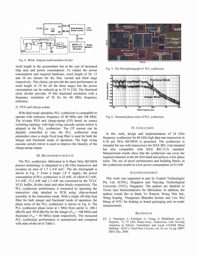
The PLL synthesizer, fabricated in O.lS�m SiGe BiCMOS
process technology is integrated in a 60 GHz transceiver and
occupies an area of l.7 x O.S mm2. The die micrograph is
shown in Fig. 5. From a single l.S V supply, the power
conswnption of PLL synthesizer is 42 mW, of which S.2 mW,
5.4 mW, 27.2 mW and l.2 mW are consumed by the TCLC
VCO, buffer, divider chain and other blocks respectively. The
PLL synthesizer performance is measured by operating the
transceiver chip attached to PCB using chip-on-board
assembly in the transmitter mode. With a single off-chip loop
fIlter for both integer and fractional mode of operation, the
phase noise of the PLL synthesizer is shown in Fig. 6. The
PLL synthesizer phase noise at 1 MHz from carrier is -106.1
dBc/Hz and -99.S dBc/Hz for the integer (Frej= lOS MHz) and
fractional (Frej = 40 MHz) mode respectively. The measured
PLL synthesizer performance is summarized and compared
with state-of-the art in Table I.
Fig. 5. Die Microphotograph of PLL synthesizer.
·30 111 111 .401l-. '-I+ul-+�I�ill--++t+++ff!-+I-H+llit-1ic--:t±-o+ttili*, -:;d::fe-+Htiitl .5 VI� lli 1I�.
10k 100k 1M 10M Offset Frequency (Hz)
Fig. 6. Measured phase noise of PLL synthesizer.
IV. CONCLUSION
In this work, design and implementation of 24 GHz
frequency synthesizer for 60 GHz high data-rate transceiver in
O.lS �m SiGe BiCMOS is presented. The synthesizer is
intended for use with transceivers for IEEE S02.11ad standard
but also compatible with IEEE S02.15.3c standard.
Measurement results show that the synthesizer can cover the
required channels in the 60 GHz band and achieve a low phase
noise. The use of novel architectures and building blocks in
the synthesizer results in a low power consumption of 42 mW.
ACKNOWLEDGEMENT
This work was supported in part by Exploit Technologies
Pte. Ltd. (ETPL), Singapore and Nanyang Technological
University (NTU) , Singapore. The authors are thankful to
Tower Jazz Semiconductors for fabrication. In addition, the
authors would like to thank Ye Wanxin, Wong Thin Sek,
Wang Keping, Thangarasu Bharatha Kumar and Lim Wei
Meng of NTU for helping in board packaging and on-wafer
measurements.
REFERENCES
[1] A. Natarajan, A. Komijani, G. Xiang, A. Babakhani, and A. Hajimiri, "A 77 GHz Phase-Array Transceiver with On-chip Antennas in Silicon: Transmitter and Local LO-Path Phase Shifting," IEEE 1. Solid State Circuits, vol. 41, no. 12, pp. 2807-2819, Dec. 2006.

TABLE I
PERFORMANCE SUMMARY AND COMPARISON OF PLL SYNTHESIZER Reference This Work This Work [3]
Technology (nm) 180 SiGe BiCMOS 180 SiGe BiCMOS 130 SiGe BiCMOS
Supply (V) 1.8 1.8 1.2,2.7 VCO Frequency (GHz) 22.5 -26.23 22.5 -26.23 15.92-18.81
PLL type Integer Fractional Sub-Integer
Frer(MHz) 108 40 285.714 Filter type External External Internal
PN (dBc/Hz)
In-band (100 kHz) -76.4 -69.8 -91.2 I MHz -106.1 -99.8 -101.9
Out-of-band (10 MHz) -124.7 -ll8.8 -122.2 Power (mW) 42 42 144
Reference spur (dBc) -35 -40 -60 Area (mm') 1.7 x 0.8 1.7 x 0.8 0.68 x I
[2] A. M. Niknejad, et ai, "Next generation CMOS compact models for RF and microwave applications," 2005 IEEE Radio Freq. Int. Cir. Symp. Dig., pp. 141-144, June 2006.
[3] B. A. Floyd, "A 16-18.8-GHz sub-integer-N frequency synthesizer for 60-GHz transceivers," IEEE J. Solid State Circuits, vol. 43, no. 5, pp. 1076 -1086, May 2008.
[4] O. Richard, et ai, "A 17.5-to-20.94GHz and 35-to-41.88GHz PLL in 65nm CMOS for wireless HD applications," ISSCC Dig. Tech. Papers, pp. 252-253, Feb. 2010.
[5] J. F. Osorio, C. S. Yaucher, B. Huff, E. Y. D. Heijden, A. D. Graauw, "A 21.7-to-27.8GHz 2.6-Degrees-rms 40mW Frequency Synthesizer in 45nm CMOS for mm-Wave Communication Applications," ISSCC Dig. Tech. Papers, pp. 278-279, Feb. 2011.
[6] K. Okada, et aI. , "A 60GHz 16QAM/8PSKlQPSKlBPSK DirectConversion Transceiver for IEEE 802.15.3c," ISSCC Dig. Tech. Papers, pp. 160-161, Feb. 2011.
[7] M. Ferriss, et aI., "An Integral Path Self-Calibration Scheme for a Dual-Loop PLL," IEEE J. Solid State Circuits, vol. 48, no. 4, pp. 996 -1008, April 2013.
[8] N. Mahalingam, K. Ma, K. S. Yeo, and W. M. Lim, "K-band High-PAE Wide-Tuning-Range YCO Using Triple-Coupled LC Tanks," IEEE Trans. Circuits Syst.ll, Exp. Briefs, vol. 60, no. 11, pp. 736-740, Nov. 2013.
[9] S. X. Mou, K. Ma, K. S. Yeo, B. K. Thangarasu, and N. Mahalingam, "A DC to 30GHz ultra-wideband CMOS T/R switch" in Semi. Coni, Dresden, pp. 1-4, Sep. 2011.
[10] Y. Wang, K. Ma, N. Mahalingam, and K. S. Yeo, "A DeltaSigma Fractional-N Frequency Divider for A Phase Lock Loop in 60GHz Transceiver" in Elec. Solid State Circuit Coni, pp. 1-2, Nov. 2011.
[4] [5] [6] [7] 65 CMOS 45 CMOS 65 CMOS 32 SOT
1.2, 1.8 0.9, 1.1, 1.8 1.0, 1.2 0.9 17.5 -20.94 21.69-27.85 17.9-21.2 21.8 -27.5
Integer Integer Integer Integer
36 48 36 195.3125 External External External Internal
-65 -88 -75 -75 -100 -95 -106 -98.8 -125 -121 -126 -126.7 80 40 66 33
<-50 -50 <-58 -
1.1 x I 0.48 x 0.29 - 1.27 x 0.87