
9sffid
36
Electric Drives 1 ELECTRIC DRIVES Ion Boldea S.A.Nasar 1998
-
Upload
deepak-velusamy -
Category
Documents
-
view
218 -
download
0
Transcript of 9sffid

7/28/2019 9sffid
http://slidepdf.com/reader/full/9sffid 1/36
Electric Drives 1
ELECTRIC DRIVES
Ion Boldea S.A.Nasar
1998
7/28/2019 9sffid
http://slidepdf.com/reader/full/9sffid 2/36
Electric Drives 2
3. POWER ELECTRONIC CONVERTERS
(P.E.Cs) FOR DRIVES
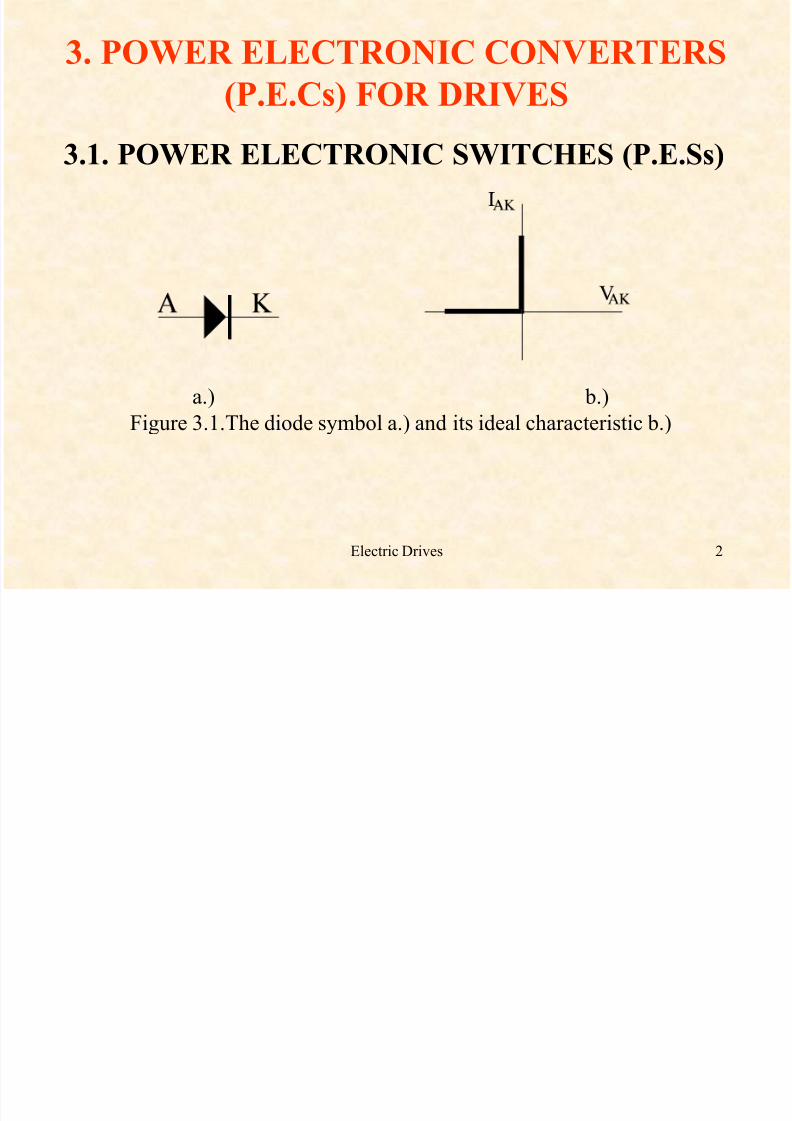
3.1. POWER ELECTRONIC SWITCHES (P.E.Ss)
a.) b.)
Figure 3.1.The diode symbol a.) and its ideal characteristic b.)

7/28/2019 9sffid
http://slidepdf.com/reader/full/9sffid 3/36
Electric Drives 3
The thyristor is used especially in P.E.Cs having an interface with a.c. power
grids, at high power levels and low commutation frequencies (up to 300Hz in
general).
a.) b.)
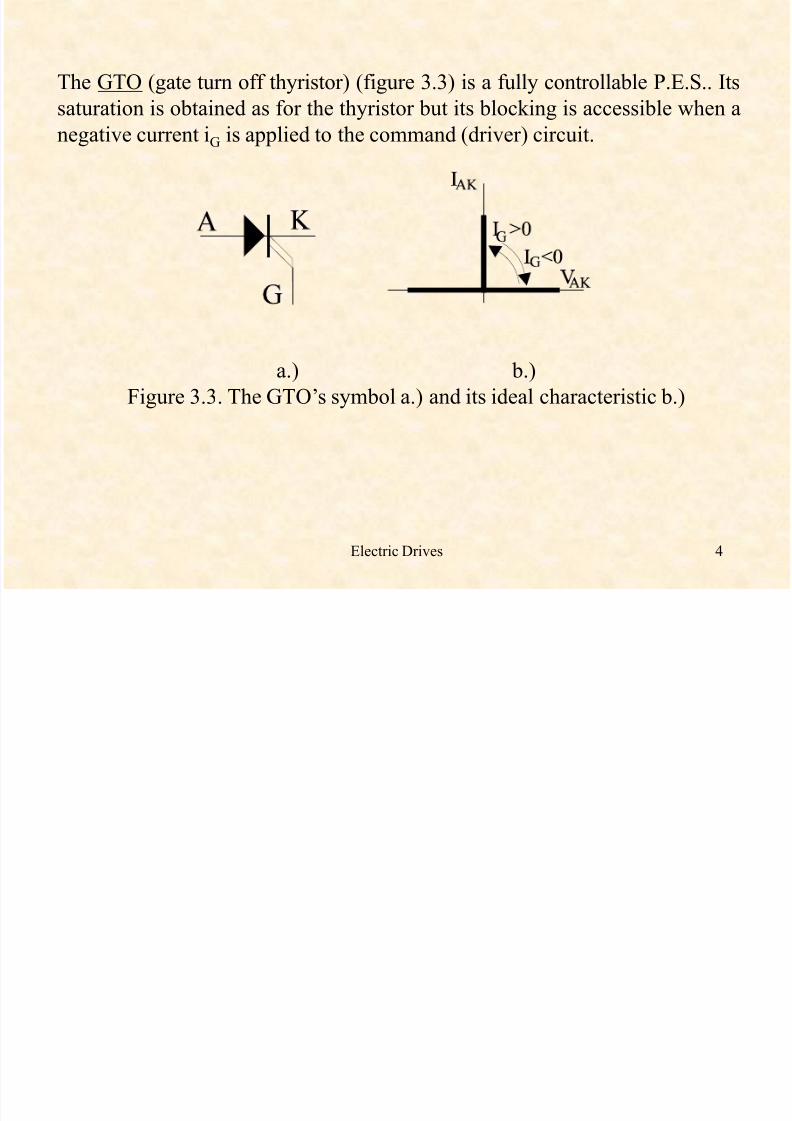
Figure 3.3. The GTO’s symbol a.) and its ideal characteristic b.)
7/28/2019 9sffid
http://slidepdf.com/reader/full/9sffid 4/36
Electric Drives 4
The GTO (gate turn off thyristor) (figure 3.3) is a fully controllable P.E.S.. Its
saturation is obtained as for the thyristor but its blocking is accessible when a
negative current iG is applied to the command (driver) circuit.
a.) b.)
Figure 3.3. The GTO’s symbol a.) and its ideal characteristic b.)

7/28/2019 9sffid
http://slidepdf.com/reader/full/9sffid 5/36
Electric Drives 5
a.) b.)
Figure 3.4. The bipolar junction transistor symbol a.) and its idealcharacteristic b.)
a.) b.)
Figure 3.5. MOS transistor symbol a.) and its ideal characteristic

7/28/2019 9sffid
http://slidepdf.com/reader/full/9sffid 6/36
Electric Drives 6
a.) b.)
Figure 3.6. IGBT’s symbol a.) and its ideal characteristic b.)
The P.E.Cs may be classified in many ways. In what follows we will refer to
their input and output voltage / current waveforms and distinguish: a.c. - d.c. converters (or rectifiers);
d.c. - d.c. converters (or choppers);
a.c. - d.c. - a.c. converters (indirect a.c. - a.c. converters) - 2 stages;
a.c. - a.c. converters (direct a.c. - a.c. converters).
We should notice that a.c. - d.c. - a.c. converters contain an a.c. - d.c. sourceside converter (rectifier) and a d.c. - a.c. converter called inverter. These
converters are mostly used with a.c. motor drives of all power levels.

7/28/2019 9sffid
http://slidepdf.com/reader/full/9sffid 7/36
Electric Drives 7
3.2. THE LINE FREQUENCY DIODE
RECTIFIER FOR CONSTANT D.C. OUTPUT
VOLTAGE Vd
Figure 3.7. Diode rectifier with output filter capacitor
a. single phase b. three phase
7/28/2019 9sffid
http://slidepdf.com/reader/full/9sffid 8/36
Electric Drives 8
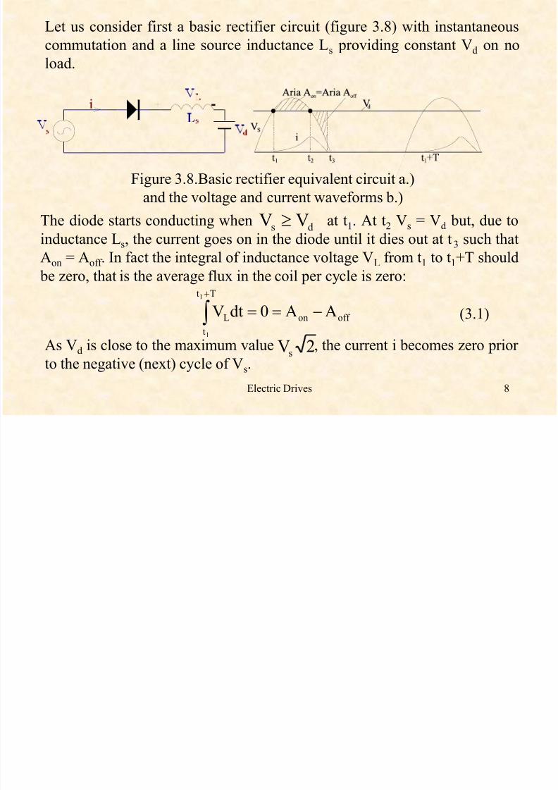
Let us consider first a basic rectifier circuit (figure 3.8) with instantaneous
commutation and a line source inductance Ls providing constant Vd on no
load.
Figure 3.8.Basic rectifier equivalent circuit a.)
and the voltage and current waveforms b.)
The diode starts conducting when at t1. At t2 Vs = Vd but, due to
inductance Ls, the current goes on in the diode until it dies out at t3 such that
Aon = Aoff . In fact the integral of inductance voltage VL from t1 to t1+T should
be zero, that is the average flux in the coil per cycle is zero:
ds VV
off on
Tt
t
L AA0dtV1
1
(3.1)
As Vd is close to the maximum value , the current i becomes zero prior
to the negative (next) cycle of Vs.2Vs
7/28/2019 9sffid
http://slidepdf.com/reader/full/9sffid 9/36
Electric Drives 9
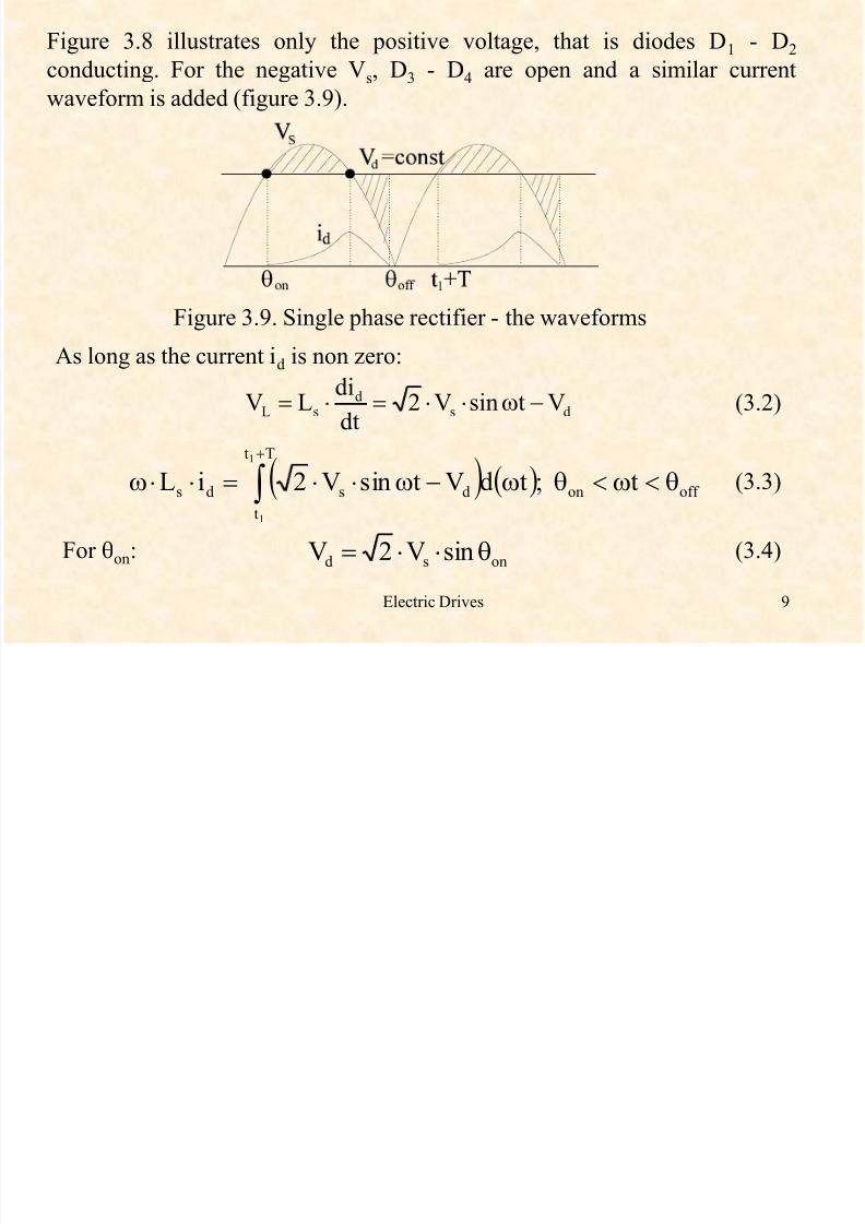
Figure 3.8 illustrates only the positive voltage, that is diodes D1 - D2
conducting. For the negative Vs, D3 - D4 are open and a similar current
waveform is added (figure 3.9).
Figure 3.9. Single phase rectifier - the waveforms
As long as the current id is non zero:
dsd
sL VtsinV2dt
diLV (3.2)
(3.3) off on
Tt
t
dsds t ;tdVtsinV2iL1
1
For on: (3.4)onsd sinV2V

7/28/2019 9sffid
http://slidepdf.com/reader/full/9sffid 10/36
Electric Drives 10
For t = off , id(t) = 0 and from (3.3) we may calculate off as a function of on.
Finally the average coil flux linkage LsId is:
tdtiL1
ILoff
on
dsds
(3.5)
For given values of LsId, iteratively on, off and finally Vd are obtained from
(3.3) - (3.5) (figure 3.10).
Figure 3.10. Vd versus LsId

7/28/2019 9sffid
http://slidepdf.com/reader/full/9sffid 11/36
Electric Drives 11
3.3. LINE CURRENT HARMONICS
WITH DIODE RECTIFIERS
The line current has the same shape as id in figure 3.9 but with alternate polarities (figure 3.11).
Figure 3.11. Source current shape
Also the current fundamental is lagging the source voltage by the
displacement power factor (DPF) angle j1:
1cosDPF j (3.6)

7/28/2019 9sffid
http://slidepdf.com/reader/full/9sffid 12/36
Electric Drives 12
The source current r.m.s. value is Is. Thus the apparent power magnitude S is:
ss IVS (3.7)
where Vs is the r.m.s. voltage value.
The power factor (3.8)
where (3.9)
So (3.10)
SPPF
DPFIVP 1ss
DPF
I
IPF
s
1s
A strong distortion in the line current will reduce the ratio Is1 / Is and thus a
small power factor PF is obtained even if DPF is unity.
Now (3.11)
2
2
s
2
1ss III
The total harmonic current distortion THD (%) is:
1s
dis
I
I100%THD (3.12)

7/28/2019 9sffid
http://slidepdf.com/reader/full/9sffid 13/36
Electric Drives 13
where (3.13)
2
2
sdis II
The peak current Ispeak is also important to be defined as a relative value constant
called the crest factor (C.F.):
s
speak
I
I.F.C (3.14)
or the form factor (F.F.):
d
s
I
I.F.F (3.15)
It has been shown that the displacement power factor DPF is above 0.9 but the
power factor PF is poor if the source inductance Ls is small.
Example 3.1.
A single phase diode rectifier with constant e.m.f. is fed from an a.c. source with
the voltage (Vs = 120V, = 367rad/s). The discontinuous
source current (figure 3.11) initiates at on = 600 and becomes zero at off = 1500.
The source inductance Ls = 5mH. Calculate the d.c. side voltage Vd and the
waveform of the source current id(t).
tsin2VtV ss

7/28/2019 9sffid
http://slidepdf.com/reader/full/9sffid 14/36
Electric Drives 14
According to figure 3.9 from (3.3) we obtain:
0tdVtsinV2off
on
ds
(3.16)
onoff doff ons VcoscosV20 (3.17)
From (3.17):
V147
3
1
6
5
150cos60cos1202Vd
(3.18)
Now from (3.3) again:
0
off d
off on
t
ds
s
d
ond
180 ;0i
for ;tdVtsinV2L
1ti
0 ;0i
on
(3.19)
7/28/2019 9sffid
http://slidepdf.com/reader/full/9sffid 15/36
Electric Drives 15
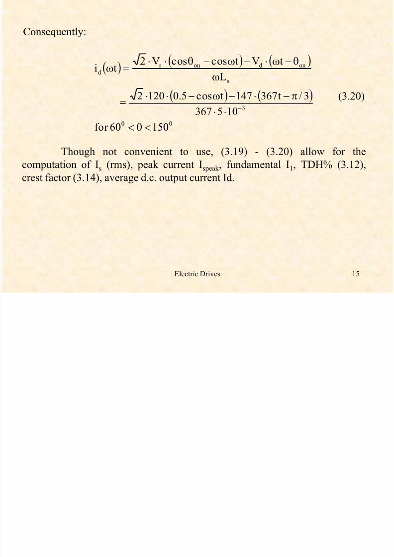
Consequently:
00
3
s
ondonsd
15006for
105367
3/t367147tcos5.01202=
L
tVtcoscosV2
ti
(3.20)
Though not convenient to use, (3.19) - (3.20) allow for the
computation of Is (rms), peak current Ispeak , fundamental I1, TDH% (3.12),
crest factor (3.14), average d.c. output current Id.

7/28/2019 9sffid
http://slidepdf.com/reader/full/9sffid 16/36
Electric Drives 16
3.4. CURRENT COMMUTATION
WITH Id = ct AND LS0
For the constant d.c. current Id = ct (figure 3.12),
Figure 3.12. Current
commutation in single sidedrectifier with Id = ct.
a.) equivalent circuit;
b.) source current;
c.) rectified voltage
a.)

7/28/2019 9sffid
http://slidepdf.com/reader/full/9sffid 17/36
Electric Drives 17
Ideally (Ls = 0), the source current will change stepwise from -Id to Id at t =
0 and t = (figure 3.12.b). Due to the nonzero Ls, during commutation, all
four diodes conduct and thus Vd = 0. For t < 0 D3D4 conduct while after
commutation (t > u) only D1D2 are on.
As Vd = 0, the source voltage during commutation is dropped solely across
inductance Ls:
td
diLtsin2V s
ss (3.21)
Through integration for the commutation interval (0,u):
ds
I
I
ss
u
0
s IL2diLtdtsin2Vd
d
(3.22)
We find:d
s
s I
2V
L21ucos
(3.23)
Now the average d.c. voltage Vd is:
ds
0dd IL2
VV
(3.24)

7/28/2019 9sffid
http://slidepdf.com/reader/full/9sffid 18/36

7/28/2019 9sffid
http://slidepdf.com/reader/full/9sffid 19/36
Electric Drives 19
3.5. THREE PHASE DIODE RECTIFIERS
In industrial applications three phase a.c. sources are available, so three phase
rectifiers seem the obvious choice (figure 3.13).
Figure 3.13. Three phase diode rectifier

7/28/2019 9sffid
http://slidepdf.com/reader/full/9sffid 20/36
Electric Drives 20
The load resistance R L with a filtering capacitor Cd may be replaced by a
constant d.c. current source Id. Using the same rationale as in the previous
paragraph we obtain:
ds
0dd IL3
VV
(3.26)
d
LL
s I
2V
L21ucos
with where VLL is the line voltage (rms).LL0d V23
V
7/28/2019 9sffid
http://slidepdf.com/reader/full/9sffid 21/36
Electric Drives 21
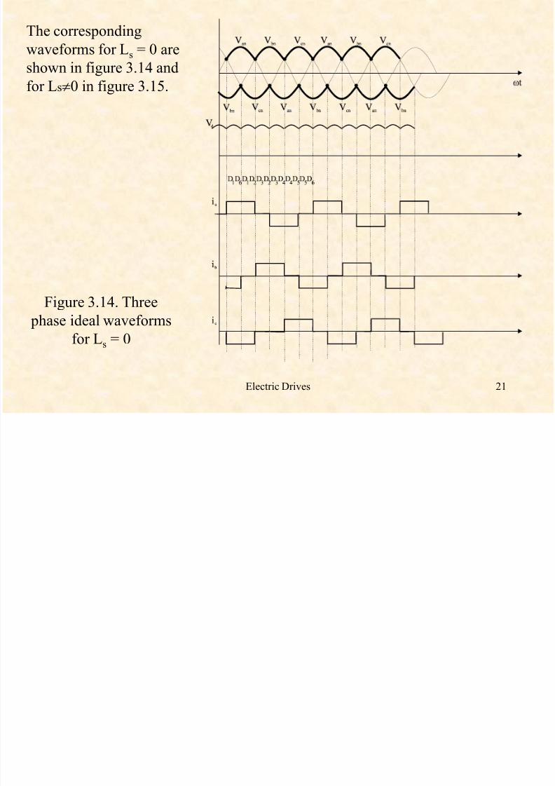
The corresponding
waveforms for Ls = 0 are
shown in figure 3.14 and
for Ls0 in figure 3.15.
Figure 3.14. Three
phase ideal waveforms
for Ls = 0
7/28/2019 9sffid
http://slidepdf.com/reader/full/9sffid 22/36
Electric Drives 22
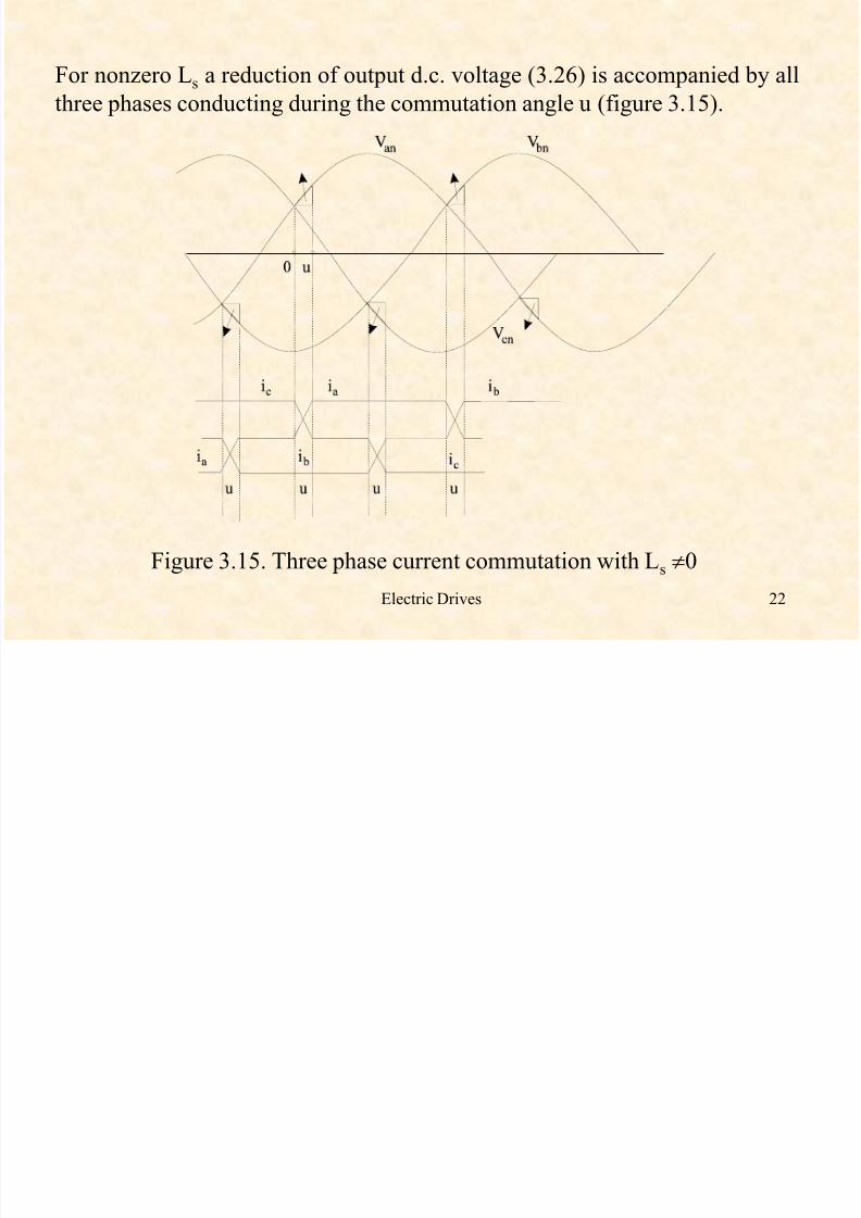
For nonzero Ls a reduction of output d.c. voltage (3.26) is accompanied by all
three phases conducting during the commutation angle u (figure 3.15).
Figure 3.15. Three phase current commutation with Ls 0

7/28/2019 9sffid
http://slidepdf.com/reader/full/9sffid 23/36
Electric Drives 23
On the other hand, for constant d.c. voltage (infinite capacitance Cd), as for the
single phase rectifier, the source current waveform is as in figure 3.16.
Figure 3.16. Three phase rectifier with finite Ls and infinite Cd (Vd = ct.) -the source current and voltage

7/28/2019 9sffid
http://slidepdf.com/reader/full/9sffid 24/36
Electric Drives 24
Example 3.3. Commutation overlapping angle u.
For a single phase or three phase a.c. system (star connection) with phase
voltage , calculate the commutation angles u, ideal no
load voltage and load voltage of single or three phase diode rectifier delivering
a constant d.c. current Id = 10A for the source inductance Ls = 5mH.
Solution:
For the single - phase diode rectifier, using (3.23):
t367sin2120tVs
783.0102120
1053672
1I2V
L2
1ucos
3
d
s
s
u = 22.7270
(3.28)
The ideal no load voltage Vd0 (3.25) is:
V10812022V22V s0d
(3.29)
V312.96101053672
108IL2
VV3
ds
0dd
(3.30)

7/28/2019 9sffid
http://slidepdf.com/reader/full/9sffid 25/36
Electric Drives 25
For the three phase diode rectifier (3.27) u is:
8746.01032120
10536721ucos
3
(3.31)
u = 12.220
Vd0 and Vd (from 3.26) are:
V66.279312023
V23
V LL0d
(3.32)
V128.262101053673
66.279IL3
VV3
ds
0dd
(3.33)
Thus the filtering capacitor Cd is notably smaller in three phase than in single
phase diode rectifiers.

7/28/2019 9sffid
http://slidepdf.com/reader/full/9sffid 26/36
Electric Drives 26
3.6. PHASE - CONTROLLED RECTIFIERS (A.C. - D.C.
CONVERTERS)
Table 3.1. Phase controlled rectifier circuits
Circuit type Powerrange
Ripplefrequency
Quadrantoperation
ia
eg
i1
La
+
-
~V1
half wavesingle
phase
below0.5KW
f s
one quadrant
B
C
half wavethree phase
up to50KW
3f s
two quadrant

7/28/2019 9sffid
http://slidepdf.com/reader/full/9sffid 27/36
Electric Drives 27
~
semi -converter
single phase
up to75KW
2f s
one quadrant
D?
A
B
C
semi -
converter three phase
up to
100K W
3f s
one quadrant
~
Full
converter single
phase
up to
75KW
2f s
two quadrant

7/28/2019 9sffid
http://slidepdf.com/reader/full/9sffid 28/36
Electric Drives 28
A
B
C
fullconverter
three phase
up to150K
W
6f s
two quadrant
~ ~
Dual
converter
single phase
up to
15KW
2f s
four quadrant
A
B
C
A
B
C
Dual
converter
three phase
up to
1500K
W
6f s
four quadrant

7/28/2019 9sffid
http://slidepdf.com/reader/full/9sffid 29/36
Electric Drives 29
3.7. D.C. - D.C. CONVERTERS (CHOPPERS)
Table 3.2. Single phase chopper configurations for d.c. brush motors
Type Chopper
configuration
ea - Ia
characteristics
Function
First
quadrant
(step down)choppers
ia
e
RaLa
D1 Va
g
+
-
io+
-
Vo
Va = V0 for S1 on
Va = 0 for S1 off
and D1 on
Secondquadrant,
regeneration(step - up)chopper
ia
e
RaLa
VaS2g
+
-
io+
-
Vo
Va = 0 for S2 onVa = V0 for S2 off
and D2 on

7/28/2019 9sffid
http://slidepdf.com/reader/full/9sffid 30/36
Electric Drives 30
Twoquadrant
chopper ia
e
RaLa
D1
S2 g
+
-
Vo
D2S1
ea = V0 for S1 or D2 onea = V0 for S2 or D1 on
ia>0 for S1 or D1 onia<0 for S2 or D2 on
Twoquadrant
chopper e
RaLa
D1
S2
g
+
-
Vo
D2
S1
Va = +V0 for S1&S2 onVa = -V0 for S1&S2 off
and D1&D2 on
Four quadrant
chopper e
RaLa
D2
S1
g
+
-
Vo
D3D1 S3
S4S2 D4
S4 on &S3 off S1&S2
operated
Va>0 ia - reversible
S2 on &S1 off S3&S4
operated
Va<0 ia - reversible

7/28/2019 9sffid
http://slidepdf.com/reader/full/9sffid 31/36
Electric Drives 31
3~
Diode
Rectifier
Braking resistor
Static switch for braking
Capacitor filter
Multiphase two quadrant chopper
Bidirect ional powe r flow
Figure 3.17. Multiphase d.c. - d.c. converters for switched reluctance motors
If an a.c. source is available a diode rectifier and filter are used in front of all
choppers (figure 3.17).

7/28/2019 9sffid
http://slidepdf.com/reader/full/9sffid 32/36
Electric Drives 32
3.8. D.C. - A.C. CONVERTERS (INVERTERS)
a.c.motor
Vo
idirectional
ower flow
Unidirectional
raking
esistor
ower flow
+
-
Figure 3.18. Voltage source PWMinverter
a. basic configuration
b. output waveforms

7/28/2019 9sffid
http://slidepdf.com/reader/full/9sffid 33/36
Electric Drives 33
a.c. motor
Io
idirectional power flow
3~
Phase
controlled
ectifier
+
-
Bidirectional po wer flow
Figure 3.19. Current source inverter
a. basic configuration
b. ideal output waveforms
a.)
b.)
7/28/2019 9sffid
http://slidepdf.com/reader/full/9sffid 34/36
Electric Drives 34
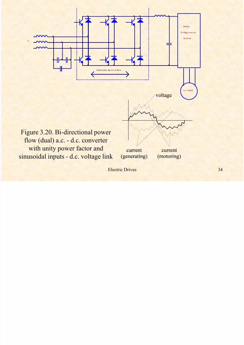
3~
a.c. motor
PWM
Vo ltage sou rce
inver ter
bidirection al p ow er flow
Figure 3.20. Bi-directional power
flow (dual) a.c. - d.c. converter
with unity power factor and
sinusoidal inputs - d.c. voltage link

7/28/2019 9sffid
http://slidepdf.com/reader/full/9sffid 35/36
Electric Drives 35
otoring
generating
3~ a.c. motor
Figure 3.21. A.c. - d.c. - a.c. converter with bi-directional power flow and unityinput power factor - d.c. current link

7/28/2019 9sffid
http://slidepdf.com/reader/full/9sffid 36/36
Electric Drives 36
3.9. DIRECT A.C. - A.C. CONVERTERS
a b
ca.c. motor
dual controlle d
rectifier (DCR) for phase a
3 secondary three phase transfor
DCR for DCR for
phase b phase c
Figure 3.22. Six - pulse
cycloconvertor for a.c. motor drives


