97.Line Following Robot
71
INDEX I ABSTRACT CHAPTER1. INTRODUCTION 1.1 Introduction 1.2 Block Diagram 1.3 Flow Chart CHAPTER2. DESCRIPTION OF HARDWARE COMPONENTS 2.1 AT89S52 2.1.1 A Brief History of 8051 2.1.2 Introduction to AT89S52 2.1.3 Features 2.1.4 Architectural Description 2.1.5 Pin Description 2.2 POWER SUPPLY 2.2.1 Introduction 2.2.2 Transformer 2.2.3 Rectifier 2.2.4 Regulator 2.3 MAX232 2.3.1 RS-232 waveform 2.3.2 RS-232 Level converter 2.3.3 Microcontroller Interfacing with RS-232 Standard devices 2.4 LDR 2.4.1 Working 2.4.2 Applications 2.5 RELAY 2.5.1 Overview 2.5.2 Relay Construction 2.5.3 Relay Applications 2.5.4 Advantages Of Relay
-
Upload
murali-krishna -
Category
Documents
-
view
255 -
download
0
Transcript of 97.Line Following Robot

5/12/2018 97.Line Following Robot - slidepdf.com
http://slidepdf.com/reader/full/97line-following-robot 1/71
INDEX
I ABSTRACT
CHAPTER1. INTRODUCTION
1.1 Introduction
1.2 Block Diagram
1.3 Flow Chart
CHAPTER2. DESCRIPTION OF HARDWARE COMPONENTS
2.1 AT89S52
2.1.1 A Brief History of 8051
2.1.2 Introduction to AT89S52
2.1.3 Features
2.1.4 Architectural Description
2.1.5 Pin Description
2.2 POWER SUPPLY
2.2.1 Introduction
2.2.2 Transformer
2.2.3 Rectifier
2.2.4 Regulator
2.3 MAX232
2.3.1 RS-232 waveform
2.3.2 RS-232 Level converter
2.3.3 Microcontroller Interfacing with RS-232 Standard devices
2.4 LDR
2.4.1 Working
2.4.2 Applications
2.5 RELAY
2.5.1 Overview
2 5 2 Relay Construction

5/12/2018 97.Line Following Robot - slidepdf.com
http://slidepdf.com/reader/full/97line-following-robot 2/71
2.5.2 Relay Construction
2.6 HELICAL GEAR MOTOR
2.7 ULN2003
2.7.1 Darlington Pair
2.7.2 Uses
CHAPTER3. CIRCUIT DIAGRAM
CHAPTER 4. SAMPLE PROGRAMS IN LAB
4.1.1 Example1
4.1.2 Example 2
4.1.3 Example 3
4.1.4 Example 4
CHAPTER 5. SOFTWARE DEVELOPMENT
5.1.1 Introduction
5.1.2 Tools used
5.1.3 C51 Compiler & A51 macro assembler
5.1.4 Start µ vision
5.1.5 over view of Keil cross compiler
5.1.6 Benefits of Keil compiler
5.1.7 Flash magic
REFERENCES

5/12/2018 97.Line Following Robot - slidepdf.com
http://slidepdf.com/reader/full/97line-following-robot 3/71
ABSTRACT
For many people robot is a machine that imitates a human—like the androids in Star Wars,
Terminator and Star Trek: The Next Generation. However much these robots capture our
imagination, such robots still only inhabit Science Fiction. People still haven't been able to
give a robot enough 'common sense' to reliably interact with a dynamic world.
Line follower is a machine that can follow a path. The path can be visible like a black line on
a white surface (or vice-versa) or it can be invisible like a magnetic field.
The type of robots that you will encounter most frequently are robots that do work that is
too dangerous, boring, onerous, or just plain nasty. Most of the robots in the world are of this
type. They can be found in auto, medical, manufacturing and space industries. In fact, there
are over a million of these type of robots working for us today.
Some robots like the Mars Rover Sojourner and the upcoming Mars Exploration Rover , or
the underwater robot Caribou help us learn about places that are too dangerous for us to go.
While other types of robots are just plain fun for kids of all ages. Popular toys such as Teckno,
Polly or AIBO ERS-220 .

5/12/2018 97.Line Following Robot - slidepdf.com
http://slidepdf.com/reader/full/97line-following-robot 4/71
a programmer you get an opportunity to ‘teach’ the robot how to follow the line thus giving it
a human-like property of responding to stimuli.
Automated cars running on roads with embedded magnets; guidance system for
industrial robots moving on shop floor etc.
CHAPTER 1
1.1 INTRODUCTION
For many people robot is a machine that imitates a human—like the androids in Star Wars,
Terminator and Star Trek: The Next Generation. However much these robots capture our
imagination, such robots still only inhabit Science Fiction. People still haven't been able to
give a robot enough 'common sense' to reliably interact with a dynamic world.
Line follower is a machine that can follow a path. The path can be visible like a black line on
a white surface (or vice-versa) or it can be invisible like a magnetic field.
The type of robots that you will encounter most frequently are robots that do work that is
too dangerous, boring, onerous, or just plain nasty. Most of the robots in the world are of this
type. They can be found in auto, medical, manufacturing and space industries. In fact, there
are over a million of these type of robots working for us today.
Some robots like the Mars Rover Sojourner and the upcoming Mars Exploration Rover , or
the underwater robot Caribou help us learn about places that are too dangerous for us to go.
While other types of robots are just plain fun for kids of all ages. Popular toys such as Teckno,

5/12/2018 97.Line Following Robot - slidepdf.com
http://slidepdf.com/reader/full/97line-following-robot 5/71
yp j p g p y ,
Sensing a line and maneuvering the robot to stay on course, while constantly correcting
wrong moves using feedback mechanism forms a simple yet effective closed loop system. As
a programmer you get an opportunity to ‘teach’ the robot how to follow the line thus giving it
a human-like property of responding to stimuli.
Automated cars running on roads with embedded magnets; guidance system for
industrial robots moving on shop floor etc.
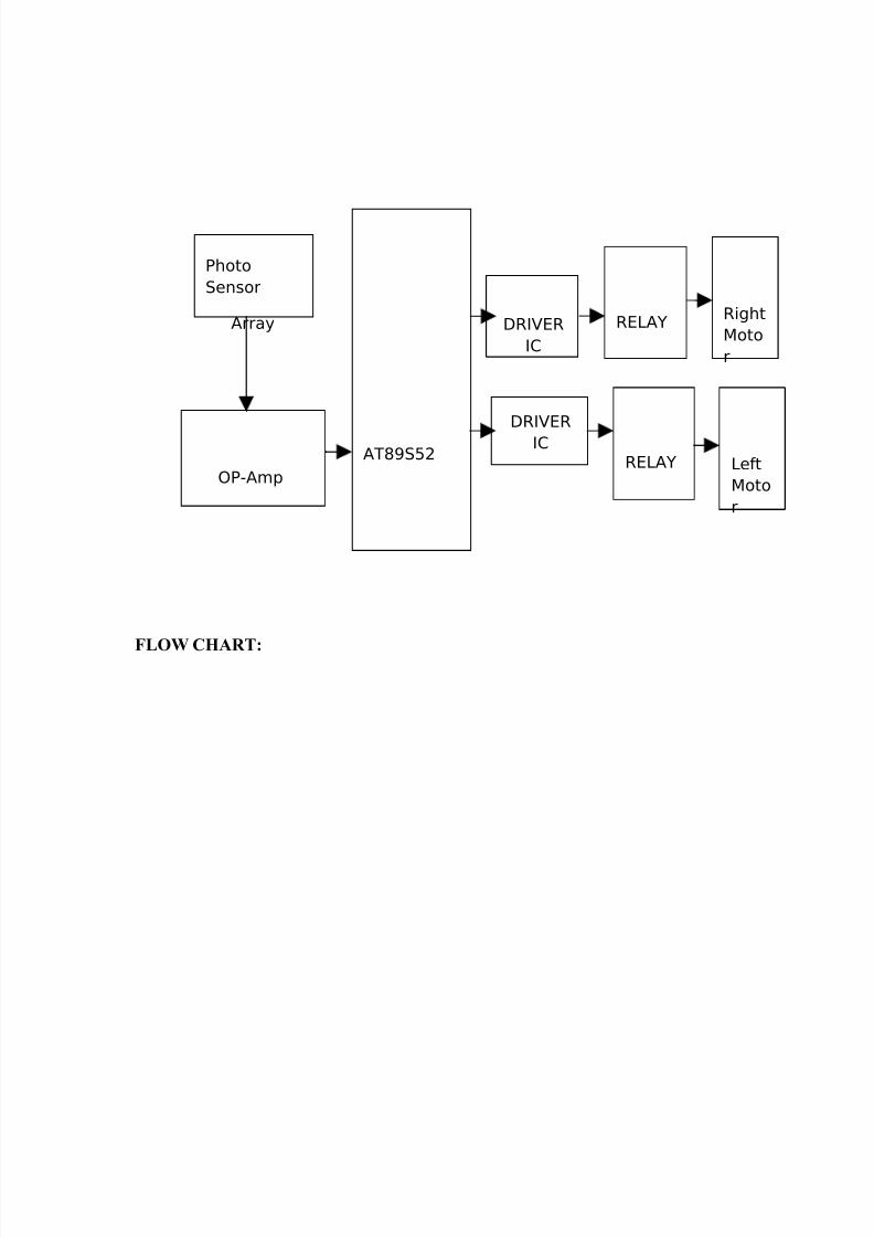
HARDWARE REQUIREMENTS:
1. MICROCONTROLLER
2. GARE MOTORS
3. DPDT RELAYS4. ULN 2003
5. LDR’S, LED’S
6. OP-AMP
SIMULATION:
TOOL: KEIL MICROVISION
LANGUAGE: EMBEDDED ‘C’
Block Diagram
5/12/2018 97.Line Following Robot - slidepdf.com
http://slidepdf.com/reader/full/97line-following-robot 6/71
FLOW CHART:
AT89S52
DRIVER
IC
DRIVER
IC
Photo
Sensor
Array
OP-Amp
RELAY
RELAY
Right
Moto
r
Left
Moto
r

5/12/2018 97.Line Following Robot - slidepdf.com
http://slidepdf.com/reader/full/97line-following-robot 7/71

5/12/2018 97.Line Following Robot - slidepdf.com
http://slidepdf.com/reader/full/97line-following-robot 8/71
CHAPTER 2
DESCRIPTION OF HARDWARE COMPONENTS
2.1 AT89S52
2.2.1 A BRIEF HISTORY OF 8051
In 1981, Intel corporation introduced an 8 bit microcontroller called 8051. this
microcontroller had 128 bytes of RAM, 4K bytes of chip ROM, two timers, one serial port,
and four ports all on a single chip. At the time it was also referred as “ A SYSTEM ON A
CHIP”
The 8051 is an 8-bit processor meaning that the CPU can work only on 8 bits data at a
time. Data larger than 8 bits has to be broken into 8 bits pieces to be processed by the CPU.
The 8051 has a total of four I\O ports each 8 bit wide.
There are many versions of 8051 with different speeds and amount of on-chip ROM
and they are all compatible with the original 8051. this means that if you write a program for
one it will run on any of them.
The 8051 is an original member of the 8051 family. There are two other
members in the 8051 family of microcontrollers. They are 8052 and 8031. All the three
microcontrollers will have the same internal architecture, but they differ in the following

5/12/2018 97.Line Following Robot - slidepdf.com
http://slidepdf.com/reader/full/97line-following-robot 9/71
• 8051 has 4K ROM, 128 bytes of RAM, two timers and 6 interrupts.
• 8052 has 8K ROM, 256 bytes of RAM, three timers and 8 interrupts.
Of the three microcontrollers, 8051 is the most preferable. Microcontroller supports
both serial and parallel communication.
In the concerned project 8052 microcontroller is used. Here microcontroller used is
AT89S52, which is manufactured by ATMEL laboratories.
NECESSITY OF MICROCONTROLLERS:
Microprocessors brought the concept of programmable devices and made many
applications of intelligent equipment. Most applications, which do not need large amount of
data and program memory, tended to be costly.
The microprocessor system had to satisfy the data and program requirements so,sufficient RAM and ROM are used to satisfy most applications .The peripheral control
equipment also had to be satisfied. Therefore, almost all-peripheral chips were used in the
design. Because of these additional peripherals cost will be comparatively high.
An example:
8085 chip needs:
An Address latch for separating address from multiplex address and data.32-KB RAM
and 32-KB ROM to be able to satisfy most applications. As also Timer / Counter, Parallel
programmable port, Serial port, and Interrupt controller are needed for its efficient
applications.
In comparison a typical Micro controller 8051 chip has all that the 8051 board has
except a reduced memory as follows.
4K bytes of ROM as compared to 32-KB, 128 Bytes of RAM as compared to 32-KB.

5/12/2018 97.Line Following Robot - slidepdf.com
http://slidepdf.com/reader/full/97line-following-robot 10/71
On comparing a board full of chips (Microprocessors) with one chip with all
components in it (Microcontroller).
Debugging:
Lots of Microprocessor circuitry and program to debug. In Micro controller there is no
Microprocessor circuitry to debug.
Slower Development time: As we have observed Microprocessors need a lot of debugging at
board level and at program level, where as, Micro controller do not have the excessive
circuitry and the built-in peripheral chips are easier to program for operation.
So peripheral devices like Timer/Counter, Parallel programmable port, Serial
Communication Port, Interrupt controller and so on, which were most often used were
integrated with the Microprocessor to present the Micro controller .RAM and ROM also were
integrated in the same chip. The ROM size was anything from 256 bytes to 32Kb or more.
RAM was optimized to minimum of 64 bytes to 256 bytes or more.
Microprocessor has following instructions to perform:
1. Reading instructions or data from program memory ROM.
2. Interpreting the instruction and executing it.
3. Microprocessor Program is a collection of instructions stored in a Nonvolatile memory.
4. Read Data from I/O device
5. Process the input read, as per the instructions read in program memory.
6. Read or write data to Data memory.
7. Write data to I/O device and output the result of processing to O/P device.
2.1.2 Introduction to AT89S52
The system requirements and control specifications clearly rule out the use of 16 32 or

5/12/2018 97.Line Following Robot - slidepdf.com
http://slidepdf.com/reader/full/97line-following-robot 11/71
The system requirements and control specifications clearly rule out the use of 16, 32 or
application is satisfactorily served by 8-bit micro controller. Using an inexpensive 8-bit
Microcontroller will doom the 32-bit product failure in any competitive market place. Coming
to the question of why to use 89S52 of all the 8-bit Microcontroller available in the market the
main answer would be because it has 8kB Flash and 256 bytes of data RAM32 I/O lines, three
16-bit timer/counters, a Eight-vector two-level interrupt architecture, a full duplex serial port,
on-chip oscillator, and clock circuitry.
In addition, the AT89S52 is designed with static logic for operation down to zero
frequency and supports two software selectable power saving modes. The Idle Mode stops the
CPU while allowing the RAM, timer/counters, serial port, and interrupt system to continue
functioning. The Power Down Mode saves the RAM contents but freezes the oscillator,
disabling all other chip functions until the next hardware reset. The Flash program memory
supports both parallel programming and in Serial In-System Programming (ISP). The 89S52
is also In-Application Programmable (IAP), allowing the Flash program memory to be
reconfigured even while the application is running.
By combining a versatile 8-bit CPU with Flash on a monolithic chip, the Atmel
AT89S52 is a powerful microcomputer which provides a highly flexible and cost effective
solution to many embedded control applications.
2.1.3 FEATURES
Compatible with MCS-51® Products
• 8K Bytes of In-System Programmable (ISP) Flash Memory
– Endurance: 1000 Write/Erase Cycles
• 4.0V to 5.5V Operating Range
• Fully Static Operation: 0 Hz to 33 MHz
• Three-level Program Memory Lock
• 256 x 8-bit Internal RAM
• 32 Programmable I/O Lines
• Three 16-bit Timer/Counters
• Eight Interrupt Sources
• Full Duplex UART Serial Channel
• Low-power Idle and Power-down Modes
I t t R f P d M d

5/12/2018 97.Line Following Robot - slidepdf.com
http://slidepdf.com/reader/full/97line-following-robot 12/71
• Interrupt Recovery from Power down Mode
-Power-off Flag
PIN DIAGRAM
5/12/2018 97.Line Following Robot - slidepdf.com
http://slidepdf.com/reader/full/97line-following-robot 13/71
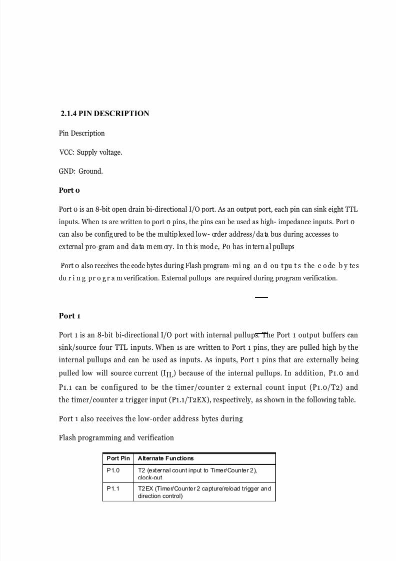
Port Pin Alternate Functions
P1.0 T2 (external count input to Timer/Counter 2),
clock-out
P1.1 T2EX (Timer/Counter 2 capture/reload trigger anddirection control)
2.1.4 PIN DESCRIPTION
Pin Description
VCC: Supply voltage.
GND: Ground.
Port 0
Port 0 is an 8-bit open drain bi-directional I/O port. As an output port, each pin can sink eight TTL
inputs. When 1s are written to port 0 pins, the pins can be used as high- impedance inputs. Port 0
can also be config ured to be the multip lexed low- order address/ da ta bus during accesses to
external pro-gram and data m em ory. In th is mod e, P0 has in tern al pullups
Port 0 also receives the code bytes during Flash program- mi ng an d ou t pu t s t he c o de b y tes
du r i n g pr o g r a m verification. External pullups are required during program verification.
Port 1Port 1 is an 8-bit bi-directional I/O port with internal pullups. The Port 1 output buffers can
sink/source four TTL inputs. When 1s are written to Port 1 pins, they are pulled high by the
internal pullups and can be used as inputs. As inputs, Port 1 pins that are externally being
pulled low will source current (IIL) because of the internal pullups. In addition, P1.0 and
P1.1 can be configured to be the timer/counter 2 external count input (P1.0/T2) and
the timer/counter 2 trigger input (P1.1/T2EX), respectively, as shown in the following table.
Port 1 also receives the low-order address bytes during
Flash programming and verification

5/12/2018 97.Line Following Robot - slidepdf.com
http://slidepdf.com/reader/full/97line-following-robot 14/71
Port 2Port 2 is an 8-bit bi-directional I/O port with internal pullups. The Port 2 output buffers can
sink/source four TTL inputs. When 1s are written to Port 2 pins, they are pulled high by the
internal pullups and can be used as inputs. As inputs, Port 2 pins that are externally beingpulled low will source current (IIL) because of the internal pullups.Port 2 emits the high-
order address byte during fetches from external program memory and during accesses
to external data memory that use 16-bit addresses (MOVX @ DPTR). In this application,
Port 2 uses strong internal pul- lups when emitting 1s. During accesses to external data
memory that use 8-bit addresses (MOVX @ RI), Port 2 emits the contents of the P2
Special Function Register.Port 2 also receives the high-order address bits and some control
signals during Flash programming and verification.
Port 3Port 3 is an 8-bit bi-directional I/O port with internal pullups. The Port 3 output buffers can
sink/source four TTL inputs. When 1s are written to Port 3 pins, they are pulled high by the
internal pullups and can be used as inputs. As inputs, Port 3 pins that are externally being
pulled low will source current (IIL) because of the pullups. Port 3 also serves the functions of
various special features of the AT89C51, as shown in the following table.
Port 3 also receives some control signals for Flash pro- gramming and verification.
Port Pin Alternate FunctionsP3.0 RXD (serial input port)
P3.1 TXD (serial output port)
P3.2 INT0 (external interrupt 0)
P3.3 INT1 (external interrupt 1)
P3.4 T0 (timer 0 external input)
P3.5 T1 (timer 1 external input)
P3.6 WR (external data memory write
P3.7 RD (external data memory read strobe)
RST

5/12/2018 97.Line Following Robot - slidepdf.com
http://slidepdf.com/reader/full/97line-following-robot 15/71
RST
device.
LE/PROG
Address Latch Enable is an output pulse for latching the low byte of the address during
accesses to external mem- ory. This pin is also the program pulse input (PROG) during Flash
programming.
In normal operation, ALE is emitted at a constant rate of 1/6 th e oscillator
frequency and may be used fo r external timing or clocking Note, however, that one ALE
pulse is skipped during each access to external data memory. If desired, ALE
operation can be disabled by setting bit 0 of SFR location 8EH. With the bit set, ALE is active
only dur-ing a MOVX or MOVC instruction. Otherwise, the pin is weakly pulled high.
Setting the ALE-disable bit has no effect if the microcontroller is in external execution
mode.

5/12/2018 97.Line Following Robot - slidepdf.com
http://slidepdf.com/reader/full/97line-following-robot 16/71
FIG-3 Functional block diagram of micro controller
The 8052 Oscillator and Clock:
The heart of the 8051 circuitry that generates the clock pulses by which all the
internal all internal operations are synchronized. Pins XTAL1 And XTAL2 is provided for
connecting a resonant network to form an oscillator. Typically a quartz crystal and capacitors
are employed. The crystal frequency is the basic internal clock frequency of the
microcontroller. The manufacturers make 8051 designs that run at specific minimum and
maximum frequencies typically 1 to 16 MHz.
Fig-4 Oscillator and timing circuit
MEMORIES
Types of memory:
The 8052 have three general types of memory. They are on-chip memory, external Code

5/12/2018 97.Line Following Robot - slidepdf.com
http://slidepdf.com/reader/full/97line-following-robot 17/71
g yp y y p y,
form of an external EPROM. External RAM is the Ram that resides off chip. This often is in the form
of standard static RAM or flash RAM.
a) Code memory
Code memory is the memory that holds the actual 8052 programs that is to be run. This
memory is limited to 64K. Code memory may be found on-chip or off-chip. It is possible to have 8K
of code memory on-chip and 60K off chip memory simultaneously. If only off-chip memory is
available then there can be 64K of off chip ROM. This is controlled by pin provided as EA
b) Internal RAM
The 8052 have a bank of 256 bytes of internal RAM. The internal RAM is found on-chip. So
it is the fastest Ram available. And also it is most flexible in terms of reading and writing. Internal
Ram is volatile, so when 8051 is reset, this memory is cleared. 256 bytes of internal memory are
subdivided. The first 32 bytes are divided into 4 register banks. Each bank contains 8 registers.
Internal RAM also contains 256 bits, which are addressed from 20h to 2Fh. These bits are bit
addressed i.e. each individual bit of a byte can be addressed by the user. They are numbered 00h to
FFh. The user may make use of these variables with commands such as SETB and CLR.
Special Function registered memory:
Special function registers are the areas of memory that control specific functionality of the
8052 micro controller.
a) Accumulator (0E0h)
As its name suggests, it is used to accumulate the results of large no of instructions. It can
hold 8 bit values.
b) B registers (0F0h)
The B register is very similar to accumulator. It may hold 8-bit value. The b register is only
used by MUL AB and DIV AB instructions. In MUL AB the higher byte of the product gets stored in
B register. In div AB the quotient gets stored in B with the remainder in A.

5/12/2018 97.Line Following Robot - slidepdf.com
http://slidepdf.com/reader/full/97line-following-robot 18/71
next value to be removed from the stack should be taken from. When a value is to be pushed onto the
stack, the 8052 first store the value of SP and then store the value at the resulting memory location.
When a value is to be popped from the stack, the 8052 returns the value from the memory location
indicated by SP and then decrements the value of SP.
d) Data pointer
The SFRs DPL and DPH work together work together to represent a 16-bit value called the
data pointer. The data pointer is used in operations regarding external RAM and some instructions
code memory. It is a 16-bit SFR and also an addressable SFR.
e) Program counter
The program counter is a 16 bit register, which contains the 2 byte address, which tells the
8052 where the next instruction to execute to be found in memory. When the 8052 is initialized PC
starts at 0000h. And is incremented each time an instruction is executes. It is not addressable SFR.
f) PCON (power control, 87h)
The power control SFR is used to control the 8051’s power control modes. Certain operation
modes of the 8051 allow the 8051 to go into a type of “sleep mode” which consumes much lee
power.
g) TCON (timer control, 88h)
The timer control SFR is used to configure and modify the way in which the 8051’s two
timers operate. This SFR controls whether each of the two timers is running or stopped and contains a
flag to indicate that each timer has overflowed. Additionally, some non-timer related bits are located
in TCON SFR. These bits are used to configure the way in which the external interrupt flags are
activated, which are set when an external interrupt occurs.
5/12/2018 97.Line Following Robot - slidepdf.com
http://slidepdf.com/reader/full/97line-following-robot 19/71
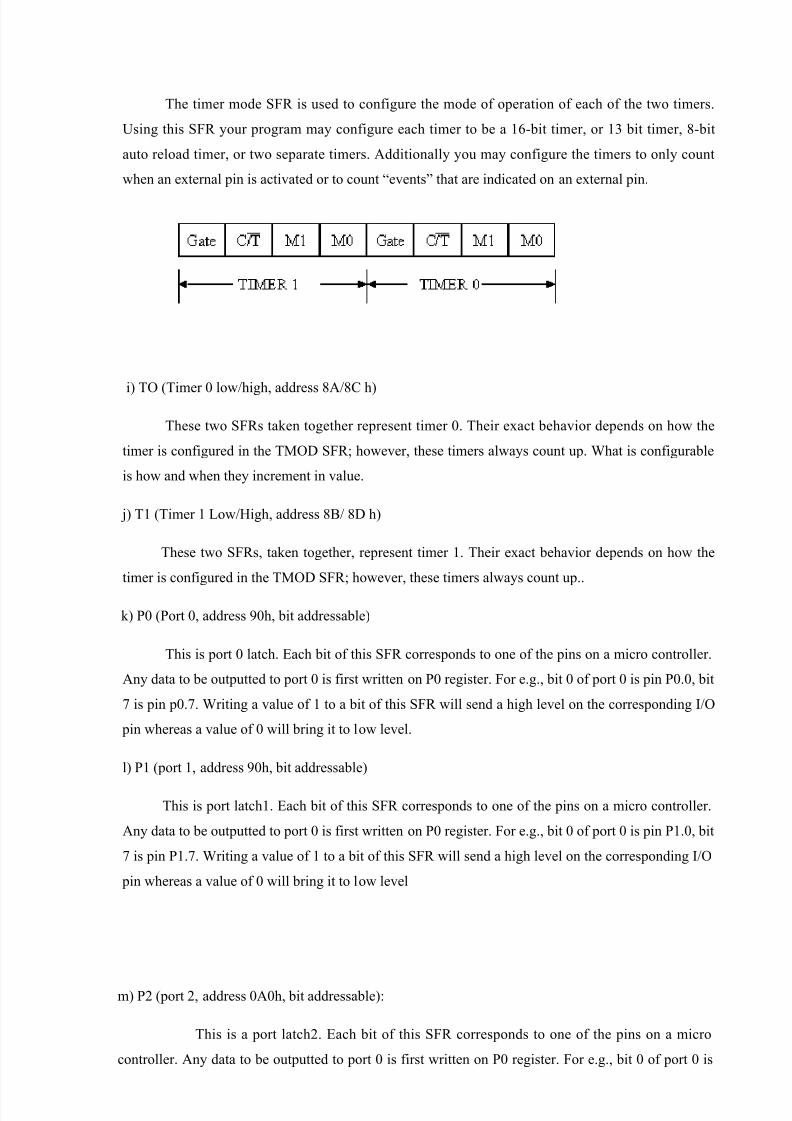
The timer mode SFR is used to configure the mode of operation of each of the two timers.
Using this SFR your program may configure each timer to be a 16-bit timer, or 13 bit timer, 8-bit
auto reload timer, or two separate timers. Additionally you may configure the timers to only count
when an external pin is activated or to count “events” that are indicated on an external pin.
i) TO (Timer 0 low/high, address 8A/8C h)
These two SFRs taken together represent timer 0. Their exact behavior depends on how the
timer is configured in the TMOD SFR; however, these timers always count up. What is configurable
is how and when they increment in value.
j) T1 (Timer 1 Low/High, address 8B/ 8D h)
These two SFRs, taken together, represent timer 1. Their exact behavior depends on how the
timer is configured in the TMOD SFR; however, these timers always count up..
k) P0 (Port 0, address 90h, bit addressable)
This is port 0 latch. Each bit of this SFR corresponds to one of the pins on a micro controller.
Any data to be outputted to port 0 is first written on P0 register. For e.g., bit 0 of port 0 is pin P0.0, bit
7 is pin p0.7. Writing a value of 1 to a bit of this SFR will send a high level on the corresponding I/O
pin whereas a value of 0 will bring it to low level.
l) P1 (port 1, address 90h, bit addressable)
This is port latch1. Each bit of this SFR corresponds to one of the pins on a micro controller.
Any data to be outputted to port 0 is first written on P0 register. For e.g., bit 0 of port 0 is pin P1.0, bit
7 is pin P1.7. Writing a value of 1 to a bit of this SFR will send a high level on the corresponding I/O
pin whereas a value of 0 will bring it to low level
m) P2 (port 2, address 0A0h, bit addressable):
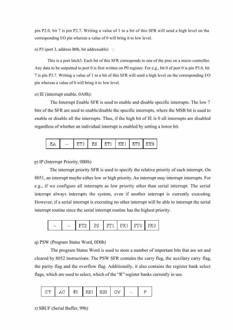
5/12/2018 97.Line Following Robot - slidepdf.com
http://slidepdf.com/reader/full/97line-following-robot 20/71
pin P2.0, bit 7 is pin P2.7. Writing a value of 1 to a bit of this SFR will send a high level on the
corresponding I/O pin whereas a value of 0 will bring it to low level.
n) P3 (port 3, address B0h, bit addressable) :
This is a port latch3. Each bit of this SFR corresponds to one of the pins on a micro controller.
Any data to be outputted to port 0 is first written on P0 register. For e.g., bit 0 of port 0 is pin P3.0, bit
7 is pin P3.7. Writing a value of 1 to a bit of this SFR will send a high level on the corresponding I/O
pin whereas a value of 0 will bring it to low level.
o) IE (interrupt enable, 0A8h):
The Interrupt Enable SFR is used to enable and disable specific interrupts. The low 7
bits of the SFR are used to enable/disable the specific interrupts, where the MSB bit is used to
enable or disable all the interrupts. Thus, if the high bit of IE is 0 all interrupts are disabled
regardless of whether an individual interrupt is enabled by setting a lower bit.
p) IP (Interrupt Priority, 0B8h)
The interrupt priority SFR is used to specify the relative priority of each interrupt. On
8051, an interrupt maybe either low or high priority. An interrupt may interrupt interrupts. For
e.g., if we configure all interrupts as low priority other than serial interrupt. The serial
interrupt always interrupts the system, even if another interrupt is currently executing.
However, if a serial interrupt is executing no other interrupt will be able to interrupt the serial
interrupt routine since the serial interrupt routine has the highest priority.
q) PSW (Program Status Word, 0D0h)
The program Status Word is used to store a number of important bits that are set and
cleared by 8052 instructions. The PSW SFR contains the carry flag, the auxiliary carry flag,
the parity flag and the overflow flag. Additionally, it also contains the register bank select
flags, which are used to select, which of the “R” register banks currently in use.

5/12/2018 97.Line Following Robot - slidepdf.com
http://slidepdf.com/reader/full/97line-following-robot 21/71
SBUF is used to hold data in serial communication. It is physically two registers. One
is writing only and is used to hold data to be transmitted out of 8052 via TXD. The other is
read only and holds received data from external sources via RXD. Both mutually exclusive
registers use address 99h.
I/O ports:
One major feature of a microcontroller is the versatility built into the input/output (I/O)
circuits that connect the 8052 to the outside world. The main constraint that limits numerous
functions is the number of pins available in the 8051 circuit. The DIP had 40 pins and the
success of the design depends on the flexibility incorporated into use of these pins. For this
reason, 24 of the pins may each used for one of the two entirely different functions which
depend, first, on what is physically connected to it and, then, on what software programs are
used to “program” the pins.
PORT 0
Port 0 pins may serve as inputs, outputs, or, when used together, as a bi directional low-
order address and data bus for external memory. To configure a pin as input, 1 must be written
into the corresponding port 0 latch by the program. When used for interfacing with the
external memory, the lower byte of address is first sent via PORT0, latched using Address
latch enable (ALE) pulse and then the bus is turned around to become the data bus for
external memory.
PORT 1
Port 1 is exclusively used for input/output operations. PORTS 1 pin have no dual
function. When a pin is to be configured as input, 1 is to be written into the corresponding
Port 1 latch.
PORT 2
Port 2 maybe used as an input/output port. It may also be used to supply a high –order
address byte in conjunction with Port 0 low-order byte to address external memory. Port 2
pins are momentarily changed by the address control signals when supplying the high byte a
16-bit address. Port 2 latches remain stable when external memory is addressed, as they do
not have to be turned around (set to 1) for data input as in the case for Port 0.
PORT 3
Port 3 may be used to input /output port. The input and output functions can be

5/12/2018 97.Line Following Robot - slidepdf.com
http://slidepdf.com/reader/full/97line-following-robot 22/71
y p p p p p
change all eight-port b se, each pin of port 3 maybe individually programmed to be used as
I/O or as one of the alternate functions. The Port 3 alternate uses are:
INTERRUPTS:
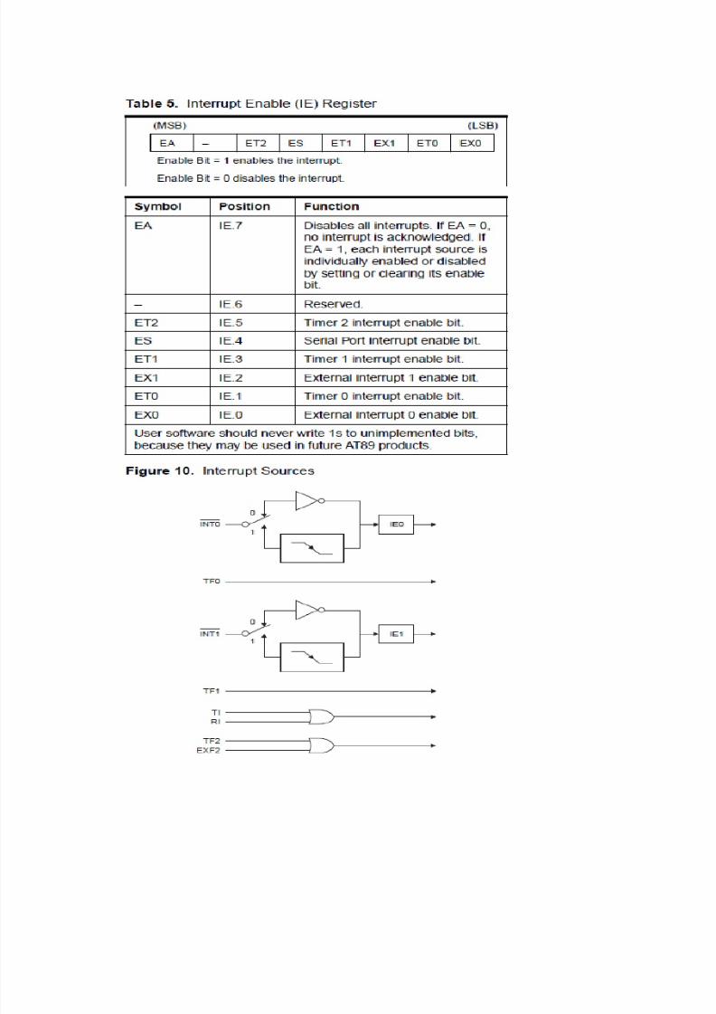
The AT89S52 has a total of six interrupt vectors: two external interrupts (INT0 and INT1),
three timer interrupts (Timers0, 1, and 2), and the serial port interrupt. These interrupts are all
shown in Figure 10. Each of these interrupt sources can be individually enabled or disabled
by setting or clearing a bit in Special Function Register IE. IE also contains a global disable
bit, EA, which disables all interrupts at once. Note that Table 5 shows that bit position IE.6 isunimplemented. In the AT89S52, bit position IE.5 is also unimplemented. User software
should not write 1s to these bit positions, since they may be used in future AT89 products.
Timer 2 interrupt is generated by the logical OR of bits TF2 and EXF2 in register T2CON.
Neither of these flags is cleared by hardware when the service routine is vectored
to. In fact, the service routine may have to determine whether it was TF2 or EXF2 that
generated the interrupt, and that bit will have to be cleared in software.The Timer 0 and Timer
1 flags, TF0 and TF1, are set at S5P2 of the cycle in which the timers overflow. The values
are then polled by the circuitry in the next cycle. However, the Timer 2 flag, TF2, is set at
Pin (SFR) Alternate UseP3.0-RXD (SBUF) Serial data input
P3.1-TXD (SBUF) Serial data output
P3.2-INTO 0 (TCON.1) External interrupt 0
P3.3 - INTO 1 (TCON.3) External interrupt 1
P3.4 - T0 (TMOD) External Timer 0 input
P3.5 – T1 (TMOD) External timer 1 input
P3.6 - WR External memory write pulse
P3.7 - RD External memory read pulse
5/12/2018 97.Line Following Robot - slidepdf.com
http://slidepdf.com/reader/full/97line-following-robot 23/71
S2 2 d i ll d i h l i hi h h i fl

5/12/2018 97.Line Following Robot - slidepdf.com
http://slidepdf.com/reader/full/97line-following-robot 24/71
2.2 Power Supply
2.2.1 INTRODUCTION
There are many types of power supply. Most are designed to convert high voltage
AC mains electricity to a suitable low voltage supply for electronics circuits and other
devices. A power supply can by broken down into a series of blocks, each of which performs
a particular function. For example a 5V regulated supply can be shown as below
Fig 2.1: Block Diagram of a Regulated Power Supply System
Similarly, 12v regulated supply can also be produced by suitable selection of
the individual elements. Each of the blocks is described in detail below and the power
supplies made from these blocks are described below with a circuit diagram and a
graph of their output:
2.2.2 Transformer:
A transformer steps down high voltage AC mains to low voltage AC. Here we
are using a center-tap transformer whose output will be sinusoidal with 36volts peak
to peak value.

5/12/2018 97.Line Following Robot - slidepdf.com
http://slidepdf.com/reader/full/97line-following-robot 25/71
Fig: 2.2.1 Output Waveform of transformer
The low voltage AC output is suitable for lamps, heaters and special AC
motors. It is not suitable for electronic circuits unless they include a rectifier and a
smoothing capacitor. The transformer output is given to the rectifier circuit.
2.2.3 Rectifier:
A rectifier converts AC to DC, but the DC output is varying. There are several
types of rectifiers; here we use a bridge rectifier.
The Bridge rectifier is a circuit, which converts an ac voltage to dc voltage
using both half cycles of the input ac voltage. The Bridge rectifier circuit is shown in
the figure. The circuit has four diodes connected to form a bridge. The ac input
voltage is applied to the diagonally opposite ends of the bridge. The load resistance is
connected between the other two ends of the bridge.
For the positive half cycle of the input ac voltage, diodes D1 and D3 conduct,
whereas diodes D2 and D4 remain in the OFF state. The conducting diodes will be inseries with the load resistance R L and hence the load current flows through R L.
For the negative half cycle of the input ac voltage, diodes D2 and D4 conduct
whereas, D1 and D3 remain OFF. The conducting diodes D2 and D4 will be in series
with the load resistance R L and hence the current flows through R L in the same
direction as in the previous half cycle. Thus a bi-directional wave is converted into
unidirectional.

5/12/2018 97.Line Following Robot - slidepdf.com
http://slidepdf.com/reader/full/97line-following-robot 26/71
Figure 2.3 Rectifier circuit
Now the output of the rectifier shown in Figure 3.3 is shown below in Figure 3.4
Figure 2.2.4 Output of the Rectifier
The varying DC output is suitable for lamps, heaters and standard motors. It is
not suitable for lamps, heaters and standard motors. It is not suitable for electronic
circuits unless they include a smoothing capacitor.
Smoothing:
The smoothing block smoothes the DC from varying greatly to a small ripple

5/12/2018 97.Line Following Robot - slidepdf.com
http://slidepdf.com/reader/full/97line-following-robot 27/71
The smoothing block smoothes the DC from varying greatly to a small ripple
Filtering is frequently effected by shunting the load with a capacitor. The
action of this system depends on the fact that the capacitor stores energy during the
conduction period and delivers this energy to the loads during the no conducting
period. In this way, the time during which the current passes through the load is
prolonging Ted, and the ripple is considerably decreased. The action of the capacitor
is shown with the help of waveform.
1) Figure 2.2.5 Smoothing action of capacitor
Figure2. 2.6 Waveform of the rectified output smoothing
2.2.4 Regulator:
Regulator eliminates ripple by setting DC output to a fixed voltage. Voltage
regulator ICs are available with fixed (typically 5V, 12V and 15V) or variable output
voltages. Negative voltage regulators are also available

5/12/2018 97.Line Following Robot - slidepdf.com
http://slidepdf.com/reader/full/97line-following-robot 28/71
Many of the fixed voltage regulator ICs has 3 leads (input, output and high
impedance). They include a hole for attaching a heat sink if necessary. Zener diode is
an example of fixed regulator which is shown here.
Figure 2.7 Regulator
Transformer + Rectifier + Smoothing + Regulator:

5/12/2018 97.Line Following Robot - slidepdf.com
http://slidepdf.com/reader/full/97line-following-robot 29/71
2.3 MAX 232
2.3.1 RS-232 WAVEFORM
TTL/CMOS Serial Logic Waveform
The diagram above shows the expected waveform from the UART
when using the common 8N1 format. 8N1 signifies 8 Data bits, No Parity and 1
Stop Bit. The RS-232 line, when idle is in the Mark State (Logic 1). A transmission
starts with a start bit which is (Logic 0). Then each bit is sent down the line, one
at a time. The LSB (Least Significant Bit) is sent first. A Stop Bit (Logic 1) is then
appended to the signal to make up the transmission.
The data sent using this method, is said to be framed. That is the
data is framed between a Start and Stop Bit.
RS-232 Voltage levels
• +3 to +25 volts to signify a "Space" (Logic 0)
• -3 to -25 volts for a "Mark" (logic 1).
• Any voltage in between these regions (i.e. between +3 and -3 Volts) is
undefined.
The data byte is always transmitted least-significant-bit first.
The bits are transmitted at specific time intervals determined by the
baud rate of the serial signal.
This is the signal present on the RS-232 Port of your computer, shown below.
RS-232 Logic Waveform

5/12/2018 97.Line Following Robot - slidepdf.com
http://slidepdf.com/reader/full/97line-following-robot 30/71
g
Standard serial interfacing of microcontroller (TTL) with PC or any
RS232C Standard device , requires TTL to RS232 Level converter . A MAX232 is
used for this purpose. It provides 2-channel RS232C port and requires external
10uF capacitors.
The driver requires a single supply of +5V.
MAX-232 includes a Charge Pump, which generates +10V and -10V from a single
5v supply.

5/12/2018 97.Line Following Robot - slidepdf.com
http://slidepdf.com/reader/full/97line-following-robot 31/71
2.3.3 MICROCONTROLLER INTERFACING WITH RS-232
STANDARD DEVICES
• MAX232 (+5V -> +-12V converter)
• Serial port male 9 pin connector (SER)
SETTING SERIAL PORT

5/12/2018 97.Line Following Robot - slidepdf.com
http://slidepdf.com/reader/full/97line-following-robot 32/71
Timer 1 Count
TH1 = 256 - ((Crystal / 384) / Baud) -PCON.7 is clear.
TH1 = 256 - ((Crystal / 192) / Baud)-PCON.7 is set.
So with PCON.7 is clear we get timer value = FDhex
Serial communication between PC and microcontroller
When a processor communicates with the outside world, it provides data in byte
sized chunks. Computers transfer data in two ways: parallel and serial. In parallel data
transfers, often more lines are used to transfer data to a device and 8 bit data path is
expensive. The serial communication transfer uses only a single data line instead of the 8 bit
data line of parallel communication which makes the data transfer not only cheaper but also
makes it possible for two computers located in two different cities to communicate over
telephone.
Serial data communication uses two methods, asynchronous and synchronous.
The synchronous method transfers data at a time while the asynchronous transfers a single
byte at a time. There are some special IC chips made by many manufacturers for data
communications. These chips are commonly referred to as UART (universal asynchronous
receiver-transmitter) and USART (universal synchronous asynchronous receiver transmitter).
The AT89C51 chip has a built in UART.
In asynchronous method, each character is placed between start and stop bits.
This is called framing. In data framing of asynchronous communications, the data, such as
ASCII characters, are packed in between a start and stop bit. We have a total of 10 bits for a
character: 8 bits for the ASCII code and 1 bit each for the start and stop bits. The rate of serial
data transfer communication is stated in bps or it can be called as baud rate.
To allow the compatibility among data communication equipment made by
various manufacturers, and interfacing standard called RS232 was set by the Electronics

5/12/2018 97.Line Following Robot - slidepdf.com
http://slidepdf.com/reader/full/97line-following-robot 33/71
standard was set long before the advent of the TTL logic family, its input and output voltage
levels are not TTL compatible. In RS232, a 1 bit is represented by -3 to -25V, while a 0 bit is
represented +3 to +25 V, making -3 to +3 undefined. For this reason, to connect any RS232 to
a microcontroller system we must use voltage converters such as MAX232 to connect the
TTL logic levels to RS232 voltage levels and vice versa. MAX232 ICs are commonly
referred to as line drivers.
The RS232 cables are generally referred to as DB-9 connector. In labeling, DB-
9P refers to the plug connector (male) and DB-9S is for the socket connector (female). The
simplest connection between a PC and microcontroller requires a minimum of three pin,
TXD, RXD, and ground. Many of the pins of the RS232 connector are used for handshaking
signals. They are bypassed since they are not supported by the 8051 UART chip.
IBM PC/ compatible computers based on x86(8086, 80286, 386, 486 and Pentium)
microprocessors normally have two COM ports. Both COM ports have RS232 type
connectors. Many PCs use one each of the DB-25 and DB-9 RS232 connectors. The COM
ports are designated as COM1 and COM2. We can connect the serial port to the COM 2 port
of a PC for serial communication experiments. We use a DB9 connector in our arrangement.
The AT89C51 has two pins that are used specifically for transferring and receiving
data serially. These two pins are called TXD and RXD and are part of the port3 (P3.0 and
P3.1). These pins are TTL compatible; therefore they require a line driver to make them
RS232 compatible. One such line driver is the MAX232 chip. One advantage of MAX232
chip is that it uses a +5v power source which is the same as the source voltage for the
at89c51. The MAX232 has two sets of line drivers for receiving and transferring data. The
line drivers for TXD are called T1 and T2 while the line drivers for RXD are designated as R1

5/12/2018 97.Line Following Robot - slidepdf.com
http://slidepdf.com/reader/full/97line-following-robot 34/71
line drivers for TXD are called T1 and T2 while the line drivers for RXD are designated as R1
and 14, respectively. The T1 in pin is the TTL side and is connected to TXD of the
microcontroller, while TI out is the RS232 side that is connected to the RXD pin of the DB9
connector.
To allow data transfer between PC and the microcontroller system without any
error, we must make sure that the baud rate of the 8051 system matches the baud rate of the
PC’s COM port.
Interrupts:-
The AT89C52 has a total of six interrupt vectors: two external interrupts (INT0
and INT1), three timer interrupts (Timers 0, 1, and 2), and the serial port interrupt. These
interrupts are all shown in Figure 5.5. Of these interrupt sources can be individually enabled
or disabled by setting or clearing a bit in Special Function Register IE. IE also contains a
global disable bit, EA, which disables all interrupts at once.
Note that Table 5.3 shows that bit position IE.6 is unimplemented. In the
AT89C51, bit position IE.5 is also unimplemented. User software should not write 1s to these
bit positions, since they may be used in future AT89 products.

5/12/2018 97.Line Following Robot - slidepdf.com
http://slidepdf.com/reader/full/97line-following-robot 35/71
Table: Interrupts Enable Register
Timer 2 interrupt is generated by the logical OR of bits TF2 and EXF2 in register
T2CON. Neither of these flags is cleared by hardware when the service routine is vectored
To. In fact, the service routine may have to determine whether it was TF2 or EXF2 that
generated the interrupt, and that bit will have to be cleared in software.
The Timer 0 and Timer 1 flags, TF0 and TF1, are set at S5P2 of the cycle in which
the timers overflow. The values are then polled by the circuitry in the next cycle. However,
the Timer 2 flag, TF2, is set at S2P2 and is polled in the same cycle in which the timer
overflows.

5/12/2018 97.Line Following Robot - slidepdf.com
http://slidepdf.com/reader/full/97line-following-robot 36/71
2.4 LDR
2.4.1 Working
A photo resistor or Light Dependent Resistor or CdS Cell is a resistor whose
resistance decreases with increasing incident light intensity. It can also be referred to as a
photoconductor. A photo resistor is made of a high resistance semiconductor . If light falling
on the device is of high enough frequency, photons absorbed by the semiconductor give
bound electrons enough energy to jump into the conduction band. The resulting free electron
(and its hole partner) conduct electricity, thereby lowering resistance.
A photoelectric device can be either intrinsic or extrinsic. An intrinsic semiconductor
has its own charge carriers and is not an efficient semiconductor, e.g. silicon. In intrinsic
devices the only available electrons are in the valence band, and hence the photon must have
enough energy to excite the electron across the entire band gap. Extrinsic devices have
impurities, also called dopants, added whose ground state energy is closer to the conduction
band; since the electrons don't have as far to jump, lower energy photons (i.e., longer

5/12/2018 97.Line Following Robot - slidepdf.com
http://slidepdf.com/reader/full/97line-following-robot 37/71
has some of its atoms replaced by phosphorus atoms (impurities), there will be extra electrons
available for conduction. This is an example of an extrinsic semiconductor.
A Light Dependent Resistor (LDR, photoconductor, or photocell) is a device which has a
resistance which varies according to the amount of light falling on its surface. They will be having a
resistance of 1 MOhm in total darkness, and a resistance of a 1 to 10 of kOhm in bright light. A
photoelectric device can be either intrinsic or extrinsic.
2.4.2 Applications:
An LDR can even be used in a simple remote control circuit using the backlight of a mobile
phone to turn on a device - call the mobile from anywhere in the world, it lights up the LDR, and
lighting can be turned on remotely!

5/12/2018 97.Line Following Robot - slidepdf.com
http://slidepdf.com/reader/full/97line-following-robot 38/71
There are two basic circuits using light dependent resistors - the first is activated by darkness,
the second is activated by light.
In the circuit diagram on the left, the led lights up whenever the LDR is in darkness. The 10K
variable resistor is used to fine-tune the level of darkness required before the LED lights up. The 10K
standard resistor can be changed as required to achieve the desired effect, although any replacement
must be at least 1K to protect the transistor from being damaged by excessive current.
By swapping the LDR over with the 10K and 10K variable resistors , the circuit will be
activated instead by light. Whenever sufficient light falls on the LDR (manually fine-tuned using the
10K variable resistor), the LED will light up.
The circuits shown above are not practically useful. In a real world circuit, the LED (and
resistor) between the positive voltage input (Vin) and the collector (C) of the transistor would be
replaced with the device to be powered.

5/12/2018 97.Line Following Robot - slidepdf.com
http://slidepdf.com/reader/full/97line-following-robot 39/71
p p
Typically a relay is used - particularly when the low voltage light detecting circuit is used to
switch on (or off) a 240V mains powered device. A diagram of that part of the circuit is shown above.
When darkness falls (if the LDR circuit is configured that way around), the relay is triggered and the
240V device - for example a security light - switches on.
Measure Light Intensity using Light Dependent Resistor (LDR):
The relationship between the resistance RL and light intensity Lux for a typical LDR is
RL = 500 / Lux Kohm
With the LDR connected to 5V through a 3.3K resistor, the output voltage of the LDR is
Vo = 5*RL / (RL+3.3)
Reworking the equation, we obtain the light intensity
Lux = (2500/Vo - 500)/3

5/12/2018 97.Line Following Robot - slidepdf.com
http://slidepdf.com/reader/full/97line-following-robot 40/71
2.5 RELAY
2.5.1 Overview
A relay is an electrically operated switch. Current flowing through the coil of the relaycreates a magnetic field which attracts a lever and changes the switch contacts. The coil
current can be ON or OFF so relays have two switch position and they are double throw
(changeover) switches.
Relays allow one circuit to switch a second circuit which can be completely separate
from the first. For example a low voltage battery circuit can use a relay to switch a 230V AC
mains circuit. There is no electrical connection inside the relay between the two circuits; the

5/12/2018 97.Line Following Robot - slidepdf.com
http://slidepdf.com/reader/full/97line-following-robot 41/71
The coil of a relay passes a relatively large current, typically 30mA for a 12V relay,
but it can be as much as 100mA for relays designed to operate from lower voltages. Most ICs
(chips) can not provide this current and a transistor is usually used to amplify the small IC
current to the larger value required for the relay coil. The maximum output current for the
popular 555 timer IC is 200mA so these devices can supply relay coils directly without
amplification.
Relays are usually SPDT or DPDT but they can have many more sets of switch
contacts, for example relay with 4 sets of changeover contacts are readily available. Most
relays are designed for PCB mounting but you can solder wires directly to the pins providing
you take care to avoid melting the plastic case of the relay.
The supplier's catalogue should show you the relay's connection. The coil will be
obvious and it may be connected either way round. Relay coils produce brief high voltage
'spikes' when they are switched off and this can destroy transistors and ICs in the circuit. To
prevent damage you must connect a protection diode across the relay coil.
The relay’s switch connections are usually contains COM, NC and NO.
COM = Common, always connect to this; it is the moving part of the switch.
NC = Normally Closed, COM is connected to this when the relay coil is off.
NO = Normally Open, COM is connected to this when the relay coil is on.
Connect to COM and NO if you want the switched circuit to be on when the relay coil is on.
Connect to COM and NC if you want the switched circuit to be on when the relay coil is off.
Most relays are SPDT or DPDT which are often described as "single pole changeover"

5/12/2018 97.Line Following Robot - slidepdf.com
http://slidepdf.com/reader/full/97line-following-robot 42/71
Most relays are SPDT or DPDT which are often described as single pole changeover
Or "double pole changeover"(DPCO).
This is a Single Pole Double Throw relay. Current will
flow between the movable contact and one fixed contact when the coil is energized and
between the movable contact and the alternate fixed contact when the relay coil is energized.
The most commonly used relay in car audio, the Bosch relay, is a SPDT relay..
This relay is a Double Pole Double Throw relay. It
operates like the SPDT relay but has twice as many contacts. There are two completely
isolated sets of contacts.

5/12/2018 97.Line Following Robot - slidepdf.com
http://slidepdf.com/reader/full/97line-following-robot 43/71
2.5.2 Relay Construction:
Relays are amazingly simple devices. There are four parts in every relay:
• Electromagnet
• Armature that can be attracted by the electromagnet
• Spring
• Set of electrical contacts
A relay consists of two separate and completely independent circuits. The first is
at the bottom and drives the electromagnet. In this circuit, a switch is controlling power to the
electromagnet. When the switch is on, the electromagnet is on, and it attracts the armature.
The armature is acting as a switch in the second circuit. When the electromagnet is energized,
the armature completes the second circuit and the light is on. When the electromagnet is not
energized, the spring pulls the armature away and the circuit is not complete. In that case, the
light is dark.
When you purchase relays, you generally have control over several variables:
The voltage and current that is needed to activate the armature
The maximum voltage and current that can run through the armature and the armature
contacts
The number of armatures (generally one or two)
The number of contacts for the armature (generally one or two -- the relay shown here
has two, one of which is unused)
Whether the contact (if only one contact is provided) is normally o pen (NO) or
normally closed (NC)

5/12/2018 97.Line Following Robot - slidepdf.com
http://slidepdf.com/reader/full/97line-following-robot 44/71
2.5.3 Relay Applications:
In general, the point of a relay is to use a small amount of power in the
electromagnet coming, say, from a small dashboard switch or a low-power electronic circuit
-- to move an armature that is able to switch a much larger amount of power. For example,
you might want the electromagnet to energize using 5 volts and 50 milliamps (250 mill
watts), while the armature can support 120V AC at 2 amps (240 watts).
Relays are quite common in home appliances where there is an electronic control
turning on something like a motor or a light. They are also common in cars, where the 12V
supply voltage means that just about everything needs a large amount of current. In later
model cars, manufacturers have started combining relay panels into the fuse box to make
maintenance easier.
In places where a large amount of power needs to be switched, relays are often
cascaded. In this case, a small relay switches the power needed to drive a much larger relay,
and that second relay switches the power to drive the load.
Relays can also be used to implement Boolean logic.
2.5.4 Advantages of Relay:
Relays can switch AC and DC, transistors can only switch DC.
Relays can switch high voltages, transistors cannot.
Relays are a better choice for switching large currents (> 5A).
Relays can switch many contacts at once.

5/12/2018 97.Line Following Robot - slidepdf.com
http://slidepdf.com/reader/full/97line-following-robot 45/71
2.6 HELICAL GEAR MOTOR:
A unit which creates mechanical energy from electrical energy and which transmits
mechanical energy through the gearbox at a reduced speed.
A gearhead and motor combination to reduce the speed of the motor to obtain the desired
speed or torque.
Gearmotors of all types and sizes including single / multiphase, universal, servo, induction
and synchronous types. DC gearmotors are configured in many types and sizes, including
brushless and servo. A DC gearmotor consists of a rotor and a permanent magnetic field stator
and an integral gearbox or gearhead. The magnetic field is maintained using either permanent
magnets or electromagnetic windings. DC motors are most commonly used in variable speed
and torque applications. A DC servomotor has an output shaft that can be positioned by
sending a coded signal to the motor. As the input to the motor changes, the angular position
of the output shaft changes as well. Servomotors are generally small and powerful for their
size, and easy to control. Common types of DC servomotors include brushless or gearmotor
types. Stepper motors are a class of motors that provide incremental motion, or steps, in
t l f t th t lt t l h th l it f th t t l t

5/12/2018 97.Line Following Robot - slidepdf.com
http://slidepdf.com/reader/full/97line-following-robot 46/71
response to pulses of current that alternately change the polarity of the stator poles; step
Important performance specifications to consider when searching for gearmotors include shaft
speed, continuous torque, continuous current, and continuous output power. The terminal
voltage is the design DC motor voltage. The continuous torque is the output torque capability
of the motor under constant running conditions. Continuous current is the maximum rated
current that can be supplied to the motor windings without overheating. Continuous output
power is the mechanical power provided by the motor output.
Important DC motor specifications to consider include terminal voltage,
motor construction and commutation. The terminal voltage is the design DC motor voltage.
Motor construction choices include permanent magnet, shunt wound, series wound,
compound wound, disc armature, and coreless or slotless. Commutation choices include
brush or brushless.
Important gearing specifications to consider for gearmotors and gearheads include the gearing
arrangement, gearbox ratio, and gearbox efficiency. Gearing arrangement choices for
gearmotors or gearheads include spur, planetary, harmonic, worm, and bevel. Gearbox ratio
is the ratio of input speed to output speed. A ratio greater than one, therefore, indicates speed
reduction, while a ratio less than one indicates speed increase. Efficiency is the percentage of
power or torque that is transferred through the gearbox. Losses occur due to factors such as
friction and slippage inside the gearbox.
Feedback choices for gearmotors include integral encoder, integral resolver, and integral
tachometer. Other important parameters to consider when specifying gearmotors include
shaft orientation or type and number of shafts, design units, motor shape, diameter or width,
housing length, NEMA frame size, enclosure options and special or extreme environment
construction. Common features include multi-speed, reversible, integral driver electronics,
integral brake, integral clutch, and brake and clutch combination.

5/12/2018 97.Line Following Robot - slidepdf.com
http://slidepdf.com/reader/full/97line-following-robot 47/71
2.7 ULN2003
ULN is mainly suited for interfacing between low-level circuits
and multiple peripheral power loads,.The series ULN20XX high voltage, high
current darlington arrays feature continuous load current ratings. The driving
circuitry in- turn decodes the coding and conveys the necessary data to the stepper
motor, this module aids in the movement of the arm through steppers
The driver makes use of the ULN2003 driver IC, which
contains an array of 7 power Darlington arrays, each capable of driving 500mA
of current. At an approximate duty cycle, depending on ambient temperature
and number of drivers turned on, simultaneously typical power loads totaling
over 230w can be controlled.
The device has base resistors, allowing direct connection to any

5/12/2018 97.Line Following Robot - slidepdf.com
http://slidepdf.com/reader/full/97line-following-robot 48/71
relays, solenoids, stepper motors, magnetic print hammers, multiplexed LED,
incandescent displays and heaters.
2.7.1 Darlington Pair
hat is a Darlington Pair?
A Darlington pair is two transistors that act as a single transistor but
with a much higher current gain.
What is current gain?
Transistors have a characteristic called current gain. This is referred to
as its hFE. The amount of current that can pass through the load when
connected to a transistor that is turned on equals the input current x the gain of
the transistor (hFE) The current gain varies for different transistor and can be
looked up in the data sheet for the device. Typically it may be 100. This would
mean that the current available to drive the load would be 100 times larger than
the input to the transistor.
2.7.2 Why use a Darlington Pair?
In some application the amount of input current available to switch on a transistor is
very low. This may mean that a single transistor may not be able to pass sufficient
current required by the load.
As stated earlier this equals the input current x the gain of the transistor (hFE). If it is
not be possible to increase the input current then we need to increase the gain of the
transistor. This can be achieved by using a Darlington Pair.

5/12/2018 97.Line Following Robot - slidepdf.com
http://slidepdf.com/reader/full/97line-following-robot 49/71
y g g
Total current gain (hFE total) = current gain of transistor 1 (hFE t1) x current gain of
transistor 2 (hFE t2)
So for example if you had two transistors with a current gain (hFE) = 100:
(hFE total) = 100 x 100
(hFE total) = 10,000
You can see that this gives a vastly increased current gain when compared to a single
transistor. Therefore this will allow a very low input current to switch a much bigger
load current.
Base Activation Voltage
Normally to turn on a transistor the base input voltage of the transistor will need to be
greater that 0.7V. As two transistors are used in a Darlington Pair this value is doubled.
Therefore the base voltage will need to be greater than 0.7V x 2 = 1.4V.
It is also worth noting that the voltage drop across collector and emitter pins of the
Darlington Pair when the turn on will be around 0.9V Therefore if the supply voltage is
5V (as above) the voltage across the load will be will be around 4.1V (5V – 0.9V)

5/12/2018 97.Line Following Robot - slidepdf.com
http://slidepdf.com/reader/full/97line-following-robot 50/71
CIRCUIT DIAGRAM

5/12/2018 97.Line Following Robot - slidepdf.com
http://slidepdf.com/reader/full/97line-following-robot 51/71
CHAPTER 4
SAMPLE PROGRAMS
Example 1:
org 00h // Starting Of The Program From 00h
memory
back: mov P1,#55h //Move 55h to Port1
acall delay // Call Delay Function
mov P1,#0AAh //Move 55h to Port1
lcall delay // Call Delay Function
sjmp back
delay: mov r5,#30h
again: djnz r5,again // Generating delay
ret // Return Of Loop
end // End Of Program
Example 2:
#include<reg51.h>
void delay(unsigned int); //Global Declaration Of Delay
void main()
{
P0=0x00; // Clearing Of Port O
while(1) //Infinite Loop
{
P0=0xAA;
delay(30);
P0=0x55;
delay(30);
}
}
5/12/2018 97.Line Following Robot - slidepdf.com
http://slidepdf.com/reader/full/97line-following-robot 52/71
}
{
unsigned int i,j;
for(i=0;i<=x;i++)
for(j=0;j<=1275;j++);
}
Example3:
#include<reg51.h>
sbit SWITCH=P1^0; // Input to P1.0
sbit LED =P2^5; // Out to P2.5
void main()
{
while(1) //Infinite Loop
{
if (SWITCH==0)
{
LED=1;
}
else
{
LED=0;
}
}
}

5/12/2018 97.Line Following Robot - slidepdf.com
http://slidepdf.com/reader/full/97line-following-robot 53/71
Example4:
#include<reg51.h>
unsigned char str[10]="MAGNI5"; // String Of Data
void main()
{
unsigned int i=0;
TMOD=0X20; // Timer1, Mode2
SCON=0X50; //1 Start Bit And 1 Stop Bit
TH1=-3; // Baud Rate 9600
TR1=1; //Start Timer 1
While(1)
{
for(i=0;i<10;i++)
{
SBUF=str[i];
while(TI==0); // Wait Data Till Bit Of Data
TI=0;
}
}
}

5/12/2018 97.Line Following Robot - slidepdf.com
http://slidepdf.com/reader/full/97line-following-robot 54/71
SOFTWARE DEVELOPMENT
5.1 Introduction:
In this chapter the software used and the language in which the program
code is defined is mentioned and the program code dumping tools are explained.
The chapter also documents the development of the program for the application.
This program has been termed as “Source code”. Before we look at the source
code we define the two header files that we have used in the code.
5.2 Tools Used:
Figure 4.1 Keil Software- internal stages
Keil development tools for the 8051 Microcontroller Architecture support every level of
software developer from the professional applications
5.3 C51 Compiler & A51 Macro Assembler:
Source files are created by the µVision IDE and are passed to the C51 Compiler or

5/12/2018 97.Line Following Robot - slidepdf.com
http://slidepdf.com/reader/full/97line-following-robot 55/71
Source files are created by the µVision IDE and are passed to the C51 Compiler or
The Keil C51 Compiler is a full ANSI implementation of the C programming
language that supports all standard features of the C language. In addition, numerous features
for direct support of the 8051 architecture have been added.
5.4µVISION
What's New in µVision3?
µVision3 adds many new features to the Editor like Text Templates, Quick
Function Navigation, and Syntax Coloring with brace high lighting Configuration
Wizard for dialog based startup and debugger setup. µVision3 is fully compatible
to µVision2 and can be used in parallel with µVision2.
What is µVision3?
µVision3 is an IDE (Integrated Development Environment) that helps you
write, compile, and debug embedded programs. It encapsulates the following
components:
• A project manager.
• A make facility.
• Tool configuration.
• Editor.
• A powerful debugger.
To help you get started, several example programs (located in the
\C51\Examples, \C251\Examples, \C166\Examples, and \ARM\...\Examples)
are provided.
• HELLO is a simple program that prints the string "Hello World" using the
Serial Interface.
• MEASURE is a data acquisition system for analog and digital systems.
• TRAFFIC is a traffic light controller with the RTX Tiny operating system.
• SIEVE is the SIEVE Benchmark.
• DHRY is the Dhrystone Benchmark.
• WHETS is the Single-Precision Whetstone Benchmark.
Additional example programs not listed here are provided for each device
architecture.
7.3 BUILDING AN APPLICATION IN µVISION
To build (compile assemble and link) an application in µVision2 you must:

5/12/2018 97.Line Following Robot - slidepdf.com
http://slidepdf.com/reader/full/97line-following-robot 56/71
To build (compile, assemble, and link) an application in µVision2, you must:
µVision2 compiles, assembles, and links the files in your project.
Creating Your Own Application in µVision2
To create a new project in µVision2, you must:
1. Select Project - New Project.
2. Select a directory and enter the name of the project file.
3. Select Project - Select Device and select an 8051, 251, or C16x/ST10
device from the Device Database™.
4. Create source files to add to the project.
5. Select Project - Targets, Groups, Files. Add/Files, select Source Group1, and
add the source files to the project.
6. Select Project - Options and set the tool options. Note when you select thetarget device from the Device Database™ all special options are set
automatically. You typically only need to configure the memory map of
your target hardware. Default memory model settings are optimal for most
applications.
7. Select Project - Rebuild all target files or Build target.
Debugging an Application in µVision2
To debug an application created using µVision2, you must:
1. Select Debug - Start/Stop Debug Session.
2. Use the Step toolbar buttons to single-step through your program. You
may enter G, main in the Output Window to execute to the main C
function.
3. Open the Serial Window using the Serial #1 button on the toolbar.
Debug your program using standard options like Step, Go, Break, and so on.
Starting µVision2 and Creating a Project
µVision2 is a standard Windows application and started by clicking on the
program icon. To create a new project file select from the µVision2 menu
Project – New Project…. This opens a standard Windows dialog that asks you
for the new project file name.
We suggest that you use a separate folder for each project. You can simply use
the icon Create New Folder in this dialog to get a new empty folder. Then

5/12/2018 97.Line Following Robot - slidepdf.com
http://slidepdf.com/reader/full/97line-following-robot 57/71
a default target and file group name. You can see these names in the Project
Window – Files.
Now use from the menu Project – Select Device for Target and select a CPU
for your project. The Select Device dialog box shows the µVision2 device
database. Just select the microcontroller you use. We are using for our examples
the Philips 80C51RD+ CPU. This selection sets necessary tool
options for the 80C51RD+ device and simplifies in this way the tool Configuration
Building Projects and Creating a HEX Files
Typical, the tool settings under Options – Target are all you need to start a
new
application. You may translate all source files and line the application with a
click on the Build Target toolbar icon. When you build an application with
syntax errors, µVision2 will display errors and warning messages in the Output
Window – Build page. A double click on a message line opens the source file
on the correct location in a µVision2 editor window. Once you have successfully
generated your application you can start debugging.
After you have tested your application, it is required to create an Intel HEX
file to download the software into an EPROM programmer or simulator. µVision2
creates HEX files with each build process when Create HEX files under Options for
Target – Output is enabled. You may start your PROM programming utility after
the make process when you specify the program under the option Run User
Program #1.
CPU Simulation
µVision2 simulates up to 16 Mbytes of memory from which areas can be
mapped for read, write, or code execution access. The µVision2 simulator traps
and reports illegal memory accesses.
In addition to memory mapping, the simulator also provides support for the

5/12/2018 97.Line Following Robot - slidepdf.com
http://slidepdf.com/reader/full/97line-following-robot 58/71
Database selection
You have made when you create your project target. Refer to page 58 for
more
Information about selecting a device. You may select and display the on-chip
peripheral components using the Debug menu. You can also change the aspects
of each peripheral using the controls in the dialog boxes.
Start Debugging
You start the debug mode of µVision2 with the Debug – Start/Stop Debug
Session command. Depending on the Options for Target – Debug
Configuration, µVision2 will load the application program and run the startup
code µVision2 saves the editor screen layout and restores the screen layout of
the last debug session. If the program execution stops, µVision2 opens an
editor window with the source text or shows CPU instructions in the disassembly
window. The next executable statement is marked with a yellow arrow. During
debugging, most editor features are still available.
For example, you can use the find command or correct program errors.
Program source text of your application is shown in the same windows. The
µVision2 debug mode differs from the edit mode in the following aspects:
⇒ The “Debug Menu and Debug Commands” described below are available.
The additional debug windows are discussed in the following.
⇒ The project structure or tool parameters cannot be modified. All build
Commands are disabled.
Disassembly Window
The Disassembly window shows your target program as mixed source and
assembly program or just assembly code. A trace history of previously executed
instructions may be displayed with Debug – View Trace Records. To enable the
trace history, set Debug – Enable/Disable Trace Recording.
If you select the Disassembly Window as the active window all program
step commands work on CPU instruction level rather than program source lines

5/12/2018 97.Line Following Robot - slidepdf.com
http://slidepdf.com/reader/full/97line-following-robot 59/71
step commands work on CPU instruction level rather than program source lines.
You may use the dialog Debug – Inline Assembly… to modify the CPU
instructions. That allows you to correct mistakes or to make temporary changes
to the target program you are debugging.
5.8 SOURCE CODE
1. Click on the Keil uVision Icon on Desktop
2. The following fig will appear
3. Click on the Project menu from the title bar
4. Then Click on New Project
5/12/2018 97.Line Following Robot - slidepdf.com
http://slidepdf.com/reader/full/97line-following-robot 60/71
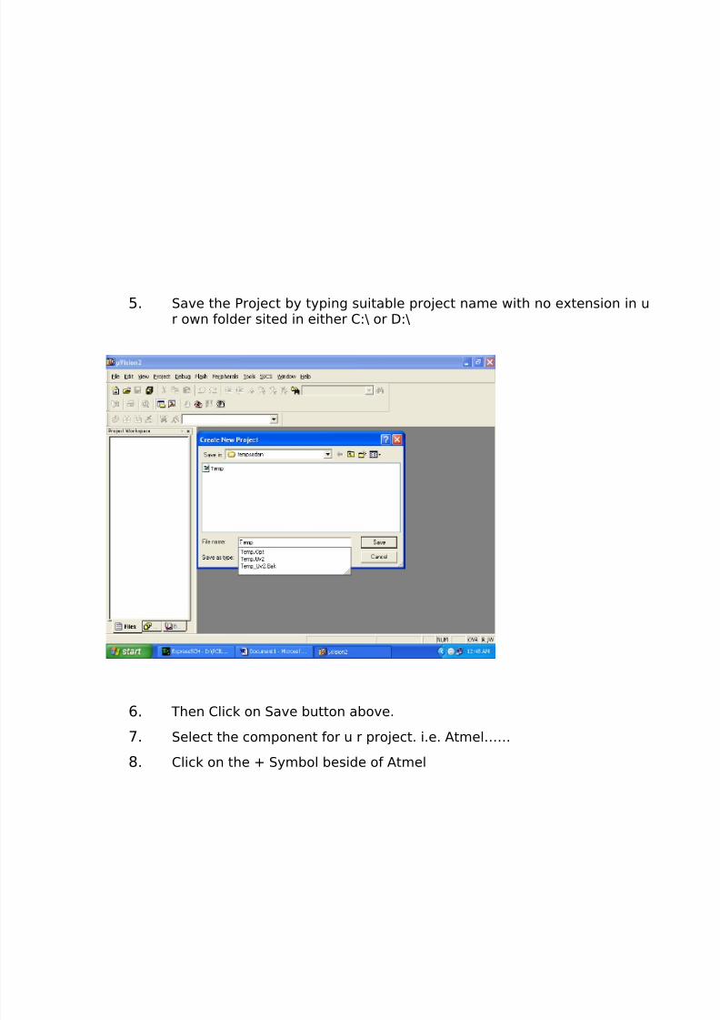
5. Save the Project by typing suitable project name with no extension in ur own folder sited in either C:\ or D:\
6. Then Click on Save button above.
7. Select the component for u r project. i.e. Atmel……
8. Click on the + Symbol beside of Atmel

5/12/2018 97.Line Following Robot - slidepdf.com
http://slidepdf.com/reader/full/97line-following-robot 61/71
9. Select AT89C51 as shown below
10. Then Click on “OK”
11. The Following fig will appear

5/12/2018 97.Line Following Robot - slidepdf.com
http://slidepdf.com/reader/full/97line-following-robot 62/71
12. Then Click either YES or NO………mostly “NO”
13. Now your project is ready to USE
14. Now double click on the Target1, you would get another option “Sourcegroup 1” as shown in next page.
15. Click on the file option from menu bar and select “new”
5/12/2018 97.Line Following Robot - slidepdf.com
http://slidepdf.com/reader/full/97line-following-robot 63/71
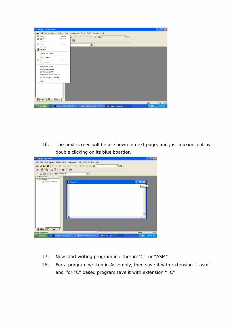
16. The next screen will be as shown in next page, and just maximize it by
double clicking on its blue boarder.
17. Now start writing program in either in “C” or “ASM”
18. For a program written in Assembly, then save it with extension “. asm”
and for “C” based program save it with extension “ .C”
5/12/2018 97.Line Following Robot - slidepdf.com
http://slidepdf.com/reader/full/97line-following-robot 64/71
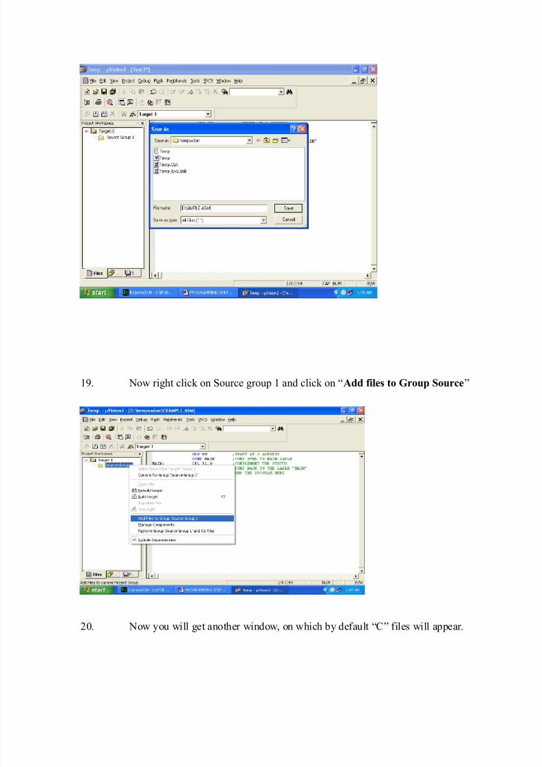
19. Now right click on Source group 1 and click on “Add files to Group Source”
20. Now you will get another window, on which by default “C” files will appear.

5/12/2018 97.Line Following Robot - slidepdf.com
http://slidepdf.com/reader/full/97line-following-robot 65/71
21. Now select as per your file extension given while saving the file
22. Click only one time on option “ADD”
23. Now Press function key F7 to compile. Any error will appear if so happen.
24. If the file contains no error, then press Control+F5 simultaneously.
25. The new window is as follows

5/12/2018 97.Line Following Robot - slidepdf.com
http://slidepdf.com/reader/full/97line-following-robot 66/71
26. Then Click “OK”
27. Now Click on the Peripherals from menu bar, and check your required port as
shown in fig below
28. Drag the port a side and click in the program file.

5/12/2018 97.Line Following Robot - slidepdf.com
http://slidepdf.com/reader/full/97line-following-robot 67/71
29. Now keep Pressing function key “F11” slowly and observe.
30. You are running your program successfully
5.6 Flash Magic:
Features:
Straightforward and intuitive user interface
Five simple steps to erasing and programming a device and setting any options
desired
Programs Intel Hex Files
Automatic verifying after programming
Fills unused flash to increase firmware security
Ability to automatically program checksums. Using the supplied checksum
calculation routine your firmware can easily verify the integrity of a Flash block,
ensuring no unauthorized or corrupted code can ever be executed
Program security bits
Check which Flash blocks are blank or in use with the ability to easily erase all blocks
in use
Read the device signature
Read any section of Flash and save as an Intel Hex File

5/12/2018 97.Line Following Robot - slidepdf.com
http://slidepdf.com/reader/full/97line-following-robot 68/71
Displays the contents of Flash in ASCII and Hexadecimal formats
Single-click access to the manual, Flash Magic home page and NXP Microcontrollers
home page
Ability to use high-speed serial communications on devices that support it. Flash
Magic calculates the highest baud rate that both the device and your PC can use and
switches to that baud rate transparently
Command Line interface allowing Flash Magic to be used in IDEs and Batch Files
Manual in PDF format
supports half-duplex communications
Verify Hex Files previously programmed
Save and open settings
Able to reset Rx2 and 66x devices (revision G or higher)
Able to control the DTR and RTS RS232 signals when connected to RST and /PSEN
to place the device into Boot ROM and Execute modes automatically. An example
circuit diagram is included in the Manual. This is essential for ISP with target
hardware that is hard to access.
This enables us to send commands to place the device in Boot ROM mode, with
support for command line interfaces. The installation includes an example project for
the Keil and Raisonance 8051 compilers that show how to build support for this
feature into applications.
Able to play any Wave file when finished programming.
built in automated version checker - helps ensure you always have the latest version.
Powerful, flexible Just In Time Code feature. Write your own JIT Modules to
generate last minute code for programming. Uses include:
o Serial number generation
o Copy protection and copy authorization
o Storing program date and time - manufacture date
o Storing program operator and location
o Lookup table generation
o Language tables or language selection
o Centralized record keeping

5/12/2018 97.Line Following Robot - slidepdf.com
http://slidepdf.com/reader/full/97line-following-robot 69/71
Requirements:
Flash Magic works on any versions of Windows, except Windows 95. 10Mb of disk
space is required. As mentioned earlier, we are automating two different routines in our
project and hence we used the method of polling to continuously monitor those tasks and act
accordingly

5/12/2018 97.Line Following Robot - slidepdf.com
http://slidepdf.com/reader/full/97line-following-robot 70/71
BIBILOGRAPHY
1. WWW.MITEL.DATABOOK.COM
2. WWW.ATMEL.DATABOOK.COM
3. WWW.FRANKLIN.COM
4. WWW.KEIL.COM
REFERENCES
1. "The 8051 Microcontroller Architecture, Programming & Applications"
By Kenneth J Ayala.
2. "The 8051 Microcontroller & Embedded Systems" by Mohammed Ali Mazidi and
Janice Gillispie Mazidi
3. "Power Electronics” by M D Singh and K B Khanchandan
4. "Linear Integrated Circuits” by D Roy Choudary & Shail Jain
5. "Electrical Machines” by S K Bhattacharya
6. "Electrical Machines II” by B L Thereja
7. www.8051freeprojectsinfo.com

5/12/2018 97.Line Following Robot - slidepdf.com
http://slidepdf.com/reader/full/97line-following-robot 71/71