Tibbals Collection, Louis E. Cooke Manuscript Collection: Cooke - Cody Correspondence
Researchers at Hong Kong University of Science and Tech-nology (HKUST) are proposing
using III-nitride and silicon carbide (SiC)hybrid technologies for high-voltagepower devices [Jin Wei et al, IEEETransactions on Electron Devices,vol63, p2469, 2016].The researchers are looking to
improve on the performance of silicon-based devices by using materials thatcan sustain higher electric fields beforebreakdown — a quality associated withwider bandgaps as seen in SiC and aluminium gallium nitride (AlGaN).SiC metal-oxide-semiconductor
field-effect transistors (MOSFETs) cansustain high OFF-state voltages but sufferfrom low channel mobility. By contrast,AlGaN/GaN high-electron-mobilitytransistors (HEMTs) have high mobility(as the device name suggests), butsuffer from problems with current col-lapse on switching due to delays fromcharge trapping. Current collapse wouldseem to restrict the potential use of lateral AlGaN/GaN HEMTs to appli-cations lower than 1000V. The problem
Technology focus: Wide-bandgap electronics
semiconductorTODAY Compounds&AdvancedSilicon • Vol. 11 • Issue 5 • June/July 2016
96
Hybrid III-nitride and silicon carbide high-voltagepower transistorsDevice simulations suggestproposal could combinehigh mobility with higherOFF-state voltages.
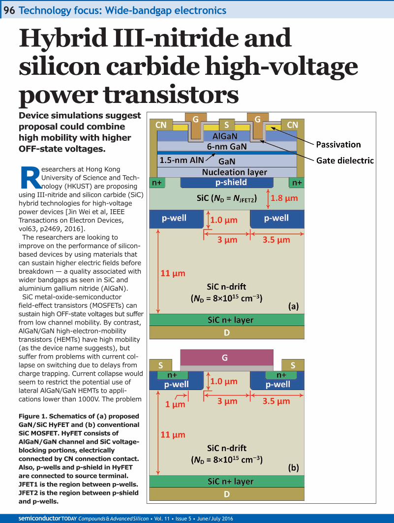
Figure 1. Schematics of (a) proposedGaN/SiC HyFET and (b) conventionalSiC MOSFET. HyFET consists ofAlGaN/GaN channel and SiC voltage-blocking portions, electricallyconnected by CN connection contact.Also, p-wells and p-shield in HyFETare connected to source terminal.JFET1 is the region between p-wells.JFET2 is the region between p-shieldand p-wells.
Technology focus: Wide-bandgap electronics
www.semiconductor-today.com semiconductorTODAY Compounds&AdvancedSilicon • Vol. 11 • Issue 5 • June/July 2016
97
could perhaps be solved by adopting a vertical structure, but this would needgrowth on very expensive GaN substrates.Some first steps have been taken, but aneffective implantation technique has yet tobe developed for creating p-type wells. The HKUST research proposes combining
III-nitride epitaxial layers on SiC to createhybrid FETs (HyFETs). The team comments:“Since epitaxial growth of GaN layers on SiC substrate is a rather mature technology,a superior power device is expected if themerits of SiC devices and GaN HEMTs arecombined on a single platform.”HKUST simulated a device with AlGaN/GaN
high-mobility channel and vertical SiC driftregion for high OFF-state voltages. In addi-tion to three HKUST researchers (Jin Wei,Qimeng Jiang, Kevin J. Chen), HuapingJiang of both Dynex Semiconductor Ltd inthe UK and Zhuzhou CRRC Times Electric Co Ltd in China contributed to the work.Dynex develops and markets high-power
bipolar discrete semiconductors, along withinsulated-gate bipolar transistors (IGBTs),electronic assemblies and components.Zhuzhou CRRC Times Electric is concernedwith propulsion and control systems forhigh-speed trains, electric multiple unit(EMUs), mass transit, and for electric anddiesel locomotives.The proposed structure (Figure 1) uses an
AlGaN/GaN channel portion for gate controlon a SiC substructure that is designed tomaintain a good OFF-state.The p-type regions of the SiC structure
could be achieved using aluminium implan-tation and activation at 1650°C. The JFET2region between the p-wells and p-shieldwould be achieved by epitaxial regrowth.The p-shield depth is 0.2µm. The AlGaN/GaN region could be grown
either by metal-organic chemical vapor dep-osition (MOCVD) or molecular beam epitaxy (MBE).Connections to the n+ (CN) and p-type regions in theSiC substructure could be achieved by dry etch of viaholes through the AlGaN/GaN layer.One aspect that does not seem to be fully developed
as yet is a high-temperature anneal for the GaN/SiCcontacts. The researchers suggest that this might needa multi-step process.Although there are a number of techniques in the
literature for giving enhancement-mode (normally-off)operation in the AlGaN/GaN structure, the researchersdecided to model a relatively new double-channel MOSgate structure that has been demonstrated by HKUST
[Jin Wei et al, IEEE Electron Device Letters, vol36,p1287, 2015]. The second channel is created by a1.5nm AlN insertion layer. The gate recess is terminatedby the upper channel at the AlGaN/GaN interface. This maintains a high mobility in the lower AlN/GaNchannel by avoiding etch degradation.One variable in the model, the n-type doping in the
JFET2 region (NJFET2), was subject to a delicate compromise between low ON-state resistance and theability to deplete the region for the OFF-state. The CN voltage used to achieve the OFF-state is higherwith high NJFET2, and this can reduce the reliability ofthe overlying AlGaN/GaN channel. The modeling
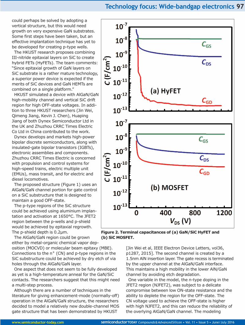
Figure 2. Terminal capacitances of (a) GaN/SiC HyFET and (b) SiC MOSFET.

Technology focus: Wide-bandgap electronics
semiconductorTODAY Compounds&AdvancedSilicon • Vol. 11 • Issue 5 • June/July 2016
98
suggested that NJFET2 of 5x10¹⁶/cm3 gave a balancebetween low ON-resistance and a relatively low OFFCN voltage of ~50V.The hybrid structure gives a sharper turn-on with
gate voltage compared with the SiC MOSFET: at 5VHyFET gate potential the ON resistance was 26mΩ-cm2,while the MOSFET at 20V gate had 4.6mΩ-cm2. The main improvement arises due to reduced channelresistance — 52% of the overall value in the MOSFET,compared with 7% for the HyFET, excluding contactand substrate resistances.The HyFET has a lower OFF-state breakdown voltage
of 1581V, compared with 1716V for the MOSFET. Thisis blamed on “more severe electric field crowding atthe corners of the p-wells”.On the other hand, the gate–drain capacitance (CGD)
of the HyFET is “dramatically reduced” — by almostthree orders of magnitude compared with the MOSFET(Figure 2). “A low CGD is of great importance in reducingthe switching loss,” the researchers write.
The HyFET setup also reduced gate charge in a simulated test circuit with supply voltage 600V andload current 100A. The circuit included a SiC Schottkybarrier diode that provided a freewheeling path. The transistors were 1cm2 in area. For the HyFET, the gate charge (QG) was found to be 239nC/cm2
and the gate–drain charge (QGD) was 47nC/cm2. The corresponding figures for the SiC MOSFET were885nC/cm2 and 223nC/cm2. The very low gate–draincharge is related to the improved CGD for the HyFET. The researchers comment: “Low values of QG and QGD
are highly desired for power FETs, since a lower QG isbeneficial for reducing the driving loss, while a lowerQGD results in a smaller switching loss.” ■http://ieeexplore.ieee.org/xpl/login.jsp?tp=&arnumber=7466844www.dynexsemi.com www.tec.csrzic.com/en/1152.html
Author: Mike Cooke
REGISTERfor Semiconductor Today
free at www.semiconductor-today.com