
956403
10
J. Nano- Electron. Phys. 1 (2009) No2, P. 8-17 2009 SumDU (Sumy State University) 8 PACS numbers: 73.40.Lq, 73.61.Ga ZnTe/CdTe THIN-FILM HETEROJUNCTIONS M.M. Kolesnyk 1 , A.S. Opanasyuk 1 , N.V. Tyrkuso va 1 , S.N. Danilchenko 2 1 Sumy State University, 2, Rimsky-Korsakov Str., 40007, Sumy, Ukraine E-mail: [email protected] 2 Institute of Applied Physics, National Academy of Science of Ukraine, 58, Petropavlivs’ka Str., 40030, Sumy, Ukraine In this work we have studied the structural and electrophysical properties of the ZnTe/CdTe heterojunctions, obtained by the method of thermal evaporation in quasi- closed volume. Investigations allowed to define the films structural parameters, such as texture, lattice constant, sizes of grains and coherent-scattering domains, micro- deformation level, and their dependence on the conditions of films productio n as well. Electrophysical investigations allowed to define the charge-transport mechanism in heterojunction. Keywords: ZnTe/CdTe HETEROJUNCTIONS, STRUCTURE FACTOR, GRAIN SIZE, CURRENT-VOLTAGE CHARACTERISTIC, CHARGE-TRANSPORT MECHANISM. (Received 25 June 2009, in final form 8 July 2009) 1. INTRODUCTION Cadmium telluride found a wide application as a basic layer of film solar cells (SC) that is conditioned by its high photosensitivity and optimal value of a band gap (BG) width for a solar energ y conve rsion [1-3 ]. Presently SC on the basis of heterojunctions (HJ) are the most challenging, where a wide band-gap semiconductor (for example, CdS) is an optical window, and CdTe is an absorbing layer. Nowadays the maximal effectiveness of SC on the basis of n-CdS/ p-CdTe heterosystems equals 16,5% [4], but possibilities of its increase are almost exhausted. It is confirmed by that during the last fifteen years the conversion efficiency (CE) of these photo-converters was succeeded in increase less than by 1% [ 5]. The main disadvantage of CdS/CdTe HJ is the formation of an interlayer of solid solutions at semiconductor interface with very high resistivity [6-7]. As a res ult, a solar ene rgy conve rsi on occurs in so-called p-i-n structures, where the p-layer consists of cadmium telluride, the n-layer consists of CdS, and the semi-insulating i-laye r is a solid solution of CdTe 1–x S x with a variable composition. This solution is characterized by a parabolic dependence of the BG versus its composition, with the minimum that equals E g 1,40 eV at x 0,21 [8]. This width is less than in basic CdTe film ( E g 1,5 eV), and as a result, in highly-defective interphase layer the intensive absorption of a solar radiation occurs that essentially decreases CE of SC. Other factors, which limit an effectiveness of photo-converters based on CdS/CdTe HJ, are the low lifetime and charge carrier mobility in cadmium telluride of p-type [1-2]. Besides, both p-CdTe and solid solution CdTe 1–x S x have low conductivity that essentially increases a series resistance of SC, and, correspondingly, decreases their CE [1-2, 6-7]. Finally, in photoconver-
Transcript of 956403
7/29/2019 956403
http://slidepdf.com/reader/full/956403 1/10
J. Nano- Electron. Phys. 1 (2009) No2, P. 8-17
2009 SumDU(Sumy State University)
8
PACS numbers: 73.40.Lq, 73.61.Ga
ZnTe/CdTe THIN-FILM HETEROJUNCTIONS
M.M. Kolesnyk1, A.S. Opanasyuk1, N.V. Tyrkusova1, S.N. Danilchenko2
1 Sumy State University,2, Rimsky-Korsakov Str., 40007, Sumy, UkraineE-mail: [email protected]
2 Institute of Applied Physics, National Academy of Science of Ukraine,58, Petropavlivs’ka Str., 40030, Sumy, Ukraine
In this work we have studied the structural and electrophysical properties of theZnTe/CdTe heterojunctions, obtained by the method of thermal evaporation in quasi-
closed volume. Investigations allowed to define the films structural parameters, suchas texture, lattice constant, sizes of grains and coherent-scattering domains, micro-
deformation level, and their dependence on the conditions of films production as well.Electrophysical investigations allowed to define the charge-transport mechanism in
heterojunction.
Keywords: ZnTe/CdTe HETEROJUNCTIONS, STRUCTURE FACTOR, GRAIN SIZE,
CURRENT-VOLTAGE CHARACTERISTIC, CHARGE-TRANSPORT MECHANISM.
(Received 25 June 2009, in final form 8 July 2009)
1. INTRODUCTION
Cadmium telluride found a wide application as a basic layer of film solarcells (SC) that is conditioned by its high photosensitivity and optimal valueof a band gap (BG) width for a solar energy conversion [1-3]. Presently SCon the basis of heterojunctions (HJ) are the most challenging, where a wide
band-gap semiconductor (for example, CdS) is an optical window, and CdTeis an absorbing layer. Nowadays the maximal effectiveness of SC on thebasis of n-CdS/ p-CdTe heterosystems equals 16,5% [4], but possibilities ofits increase are almost exhausted. It is confirmed by that during the lastfifteen years the conversion efficiency (CE) of these photo-converters wassucceeded in increase less than by 1% [5].
The main disadvantage of CdS/CdTe HJ is the formation of an interlayerof solid solutions at semiconductor interface with very high resistivity [6-7].As a result, a solar energy conversion occurs in so-called p-i-n structures,where the p-layer consists of cadmium telluride, the n-layer consists of CdS,and the semi-insulating i-layer is a solid solution of CdTe1–xSx with a variablecomposition. This solution is characterized by a parabolic dependence of theBG versus its composition, with the minimum that equals Eg 1,40 eV at
x 0,21 [8]. This width is less than in basic CdTe film (Eg 1,5 eV), and as
a result, in highly-defective interphase layer the intensive absorption of asolar radiation occurs that essentially decreases CE of SC.
Other factors, which limit an effectiveness of photo-converters based onCdS/CdTe HJ, are the low lifetime and charge carrier mobility in cadmiumtelluride of p-type [1-2]. Besides, both p-CdTe and solid solution CdTe1–xSx have low conductivity that essentially increases a series resistance of SC,and, correspondingly, decreases their CE [1-2, 6-7]. Finally, in photoconver-
7/29/2019 956403
http://slidepdf.com/reader/full/956403 2/10
ZnTe/CdTe THIN-FILM HETEROJUNCTIONS 9
ters on the basis of cadmium telluride films of p-type the problem of ohmiccontact formation to p-layer, which is not solved up to now [9], appears.
It is possible to get rid of many disadvantages of known SC HJ if usecadmium telluride with electron conduction as absorbing layer of devices.But in this case there is a problem of occurrence of a wide BG window of p-type semiconductor. In [10] as such material the ZnTe was proposed for using,which single (accept of CdTe) of compounds of A2B6 group can be easilyobtained with the hole conduction. Though zinc telluride has less BG width(Eg 2,26 eV) than cadmium sulfide (Eg 2,42 eV), it forms with CdTe asolid solution Zn1–xCdxTe, which BG is changed linearly under materialcomposition changes from values typical for CdTe to values, which ZnTe has[11]. It is important from an environmental point of view that this semi-conductor does not contain a heavy metal – cadmium – in its own composition.
According to theoretical calculations, the high density of surface statesat semiconductor interface that is conditioned by a mismatch of their latticeconstants [12] is the disadvantage of ZnTe/CdTe HJ. But as in the case of
CdS/CdTe HJ, on the interface of ZnTe and CdTe the formation of solidsolutions, which can compensate this mismatch, is expected. Unfortunately,the film ZnTe/CdTe HJ are poorly studied. And this is the reason of thepresent investigation.
In this work we have studied some structural and electrophysicalcharacteristics of p-ZnTe/n-CdTe HJ and separate layers in this structure.
2. RESEARCH TECHNIQUE
p-ZnTe/n-CdTe HJ were produced using the technique described in detail in[13]. Condensation of cadmium telluride films was realized on the cleanedglass substrates with molybdenum sublayer by the quasi-closed volumetechnique at the temperatures Te 923 K and Ts 823 K of evaporator andsubstrate, respectively. Then ZnTe layers were deposited in quasi-closed
volume as well. The evaporator temperature under condensation wasTe 973 K, and the substrate temperature varied within the range Ts 523-623 K. ZnTe film deposition was performed both on a glass substrate andCdTe sublayer. This gave an opportunity to carry out a comparative analysisof ZnTe characteristics, obtained directly on a glass and CdTe sublayer.Upper current-collecting contacts to a multi-layer structure are made ofsilver by thermal deposition in vacuum.
Surface morphology of ZnTe and CdTe films were studied by the scanningmicroscopy method (REMMA-102). An average grain size (d) in condensateswas found using the Jeffries method. The film width was measured byfractography. Structural investigations of condensates were carried outusing the X-ray diffractometer DRON 4-07 in Ni-filtered K -radiation ofcopper anode. Here, using the technique described in [13-14] the phase
composition, the lattice constant, and the layer texture were determinedfrom diffraction patterns, and the coherent-scattering domain (CSD) sizeand the microdeformation level in ZnTe condensates on a glass and CdTesublayer were found using the broadening of diffraction lines. The features ofcharge-transport in ZnTe/CdTe HJ were defined by analysis of the current-voltage characteristics obtained at different temperatures using thetechnique described in [12]. In this case the mechanism of currentpropagation through a multi-layer structure was determined.

7/29/2019 956403
http://slidepdf.com/reader/full/956403 3/10
10 M.M. KOLESNYK, A.S. OPANASYUK, N.V. TYRKUSOVA ET AL.
3. RESULTS DISCUSSION
3.1 Structural properties
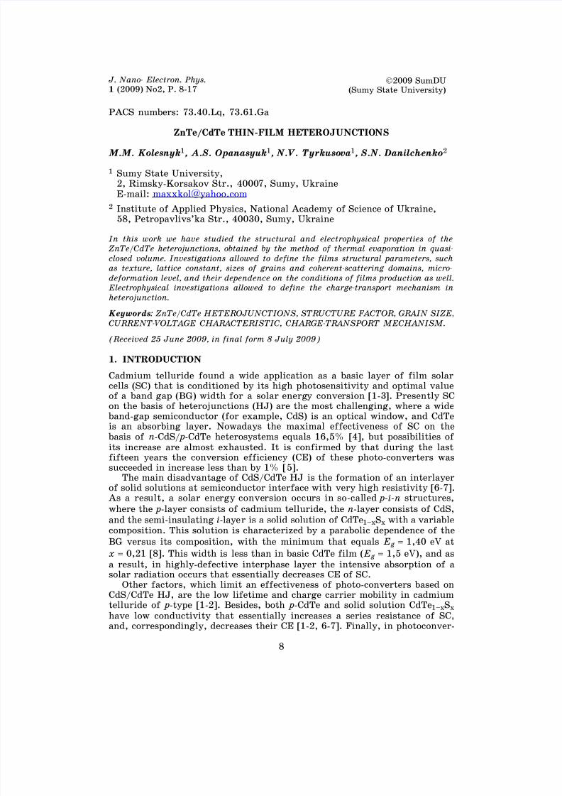
In [13-14] we have studied the structural characteristics of ZnTe thin filmsand determined the optimal manufacturing conditions of producing layerswith the best, from the viewpoint of using in devices, properties (one-phasestate, high texturing, large grain and CSD sizes, small microdeformationlevel and others): the evaporator temperature is Te 973 K, the substratetemperature is Ts 523-623 K. These regimes were used under ZnTe filmdeposition on CdTe. Similarly, CdTe layers were condensed under conditionsclosed to the thermodynamically equilibrium ones, when they had columnarstructure with large grain size [15]. The width of obtained CdTe films wasl 15 µm, condensates of ZnTe had essentially less thickness l (2,5-3,5) µm, since they should be transparent for solar radiation to the CdTeabsorbing layer.
The electron-microscopic photographs of the surface of CdTe and ZnTe
films deposited under mentioned condensation conditions directly on a glassare presented in Fig. 1a,b.As seen from the figure, CdTe films consist of grains of different
fractions, both fine (2-3 µm) and coarse (up to 10 µm). The growth steps(Fig. 1a) are well discerned on the surface of large grains. An average grainsize of the films is 5 µm. ZnTe films have more homogeneous grainstructure (Fig. 1b). But an average grain size for them is less than for CdTefilms. Thus, ZnTe films obtained at Ts 623 K had an average grain size 2 µm, while condensates deposited at Ts 523 K were quite fine-dispersed(d < 0,3 µm).
Transition regions between CdTe and ZnTe films are shown in Fig. 1c,e,and microstructure of ZnTe condensates deposited on CdTe sublayer atdifferent substrate temperatures are represented in Fig. 1d,f. As seen fromthese figures, since ZnTe films are thin enough, they completely repeat the
surface structure of CdTe sublayer. In this case the CdTe grain boundariesare well seen on the micrographs (Fig. 1d,f). In ZnTe films (Fig. 1d)deposited on CdTe sublayer at low temperatures (Ts 523 K) increase of thegrain size is not observed in comparison with condensates deposited directlyon a glass. This implies about the same growth mechanism of ZnTe films ona glass and CdTe sublayer. It is described in detail in [13]. But in more high-temperature condensates (Ts 623 K) the deposition on CdTe sublayer
leaded to small increase of grain size from 2 µm to 2,5 µm. In this casethe grain shape of ZnTe films was slightly changing as well. This points outthat under deposition of high-temperature condensates the heteroepitaxialformation of ZnTe nucleus on CdTe film surface is possible.
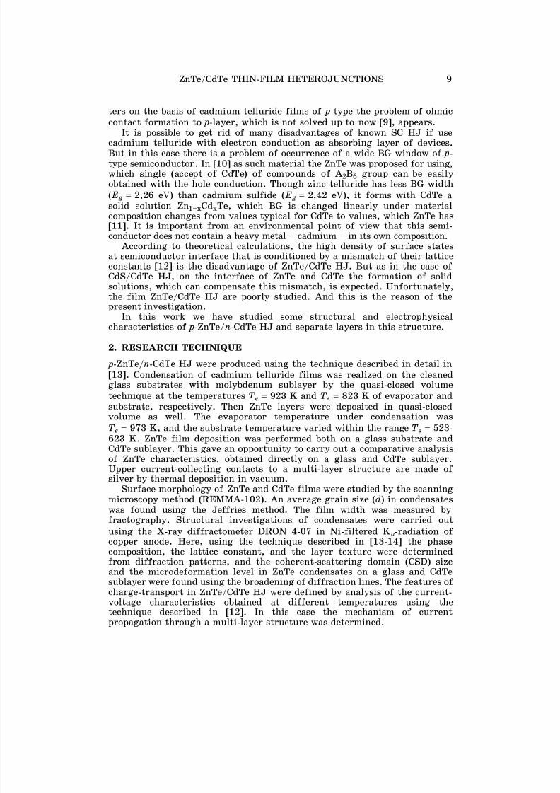
Cross-section of ZnTe/CdTe HJ is illustrated in Fig. 2. The thick CdTefilm coated by the thinner ZnTe layer is seen there. The large grains are
observed in CdTe film, but unfortunately grains are not discerned in ZnTelayer.
7/29/2019 956403
http://slidepdf.com/reader/full/956403 4/10
ZnTe/CdTe THIN-FILM HETEROJUNCTIONS 11
Fig. 1 – Microstructure of the CdTe (a) and ZnTe (b) film surface on a glass;transition region between ZnTe and CdTe films (c, e); ZnTe on CdTe sublayer (d, f).
Condensation conditions for CdTe: Te 923 K, Ts
823 K (a, c, e ); for ZnTe :
Te 973 K, Ts 523 K (c, d); Ts 623 K (b, e, f)
Fig. 2 – Cross-section of ZnTe/CdTe HJ. Condensation conditions for ZnTe film:
Te 973 K, Ts 523 K
a b
c
e
d
f

7/29/2019 956403
http://slidepdf.com/reader/full/956403 5/10
12 M.M. KOLESNYK, A.S. OPANASYUK, N.V. TYRKUSOVA ET AL.
Typical X-ray diffraction (XRD) patterns obtained from ZnTe films ona glass and ZnTe/CdTe HJ are represented in Fig. 3. Films on a glass werethe single-phase ones with sphalerite structure and strongly pronounced
texture [111] [13]. The XRD analysis from a double-layer structure showedthat only reflection from crystallographic planes, which correspond to theZnTe and CdTe cubic phases, is fixed here as well. The presence of solidsolutions in heterosystems has not been detected by X-ray investigation, andthis gave an opportunity to suppose that the HJ we have obtained aresufficiently abrupt.
Fig 3 – XRD patterns from ZnTe films on a glass (a, c) and ZnTe sublayer (b, d)
obtained at different substrate temperatures: Ts 523 K (a, b), Ts 623 K (c, d)
As seen from Fig. 3b,d, the peaks (111) and (222) on the angles 2 25,33 and 51,80 for ZnTe and the peak (111) on the angle 2 23,72 for CdTeare dominant ones by intensity on the XRD patterns. This implies aboutboth CdTe and ZnTe film texturing. The calculation results of the structure
factor (f ), which characterizes the structural perfection of ZnTe films on aglass and CdTe, are represented in Table 1. It is possible to see that CdTesublayer does not almost change the texture quality of ZnTe condensatedeposited at lower substrate temperatures (Ts 523 K) and increases it inthe case of a film deposited at higher temperatures (Ts 623 K). This effectcan be explained by the heteroepitaxial ZnTe nucleation on strongly texturedCdTe films as well.
a b
c d
I n t e n s i t y ,
%
I n t e n s i t y ,
%
I n
t e n s i t y ,
%
I n
t e n s i t y ,
%
7/29/2019 956403
http://slidepdf.com/reader/full/956403 6/10
ZnTe/CdTe THIN-FILM HETEROJUNCTIONS 13
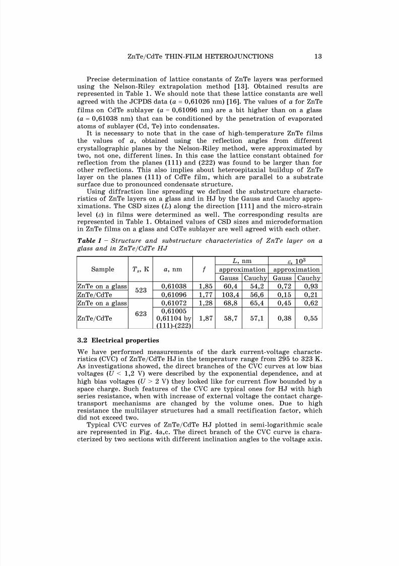
Precise determination of lattice constants of ZnTe layers was performedusing the Nelson-Riley extrapolation method [13]. Obtained results arerepresented in Table 1. We should note that these lattice constants are well
agreed with the JCPDS data (a 0,61026 nm) [16]. The values of a for ZnTefilms on CdTe sublayer (a 0,61096 nm) are a bit higher than on a glass(a 0,61038 nm) that can be conditioned by the penetration of evaporatedatoms of sublayer (Cd, Te) into condensates.
It is necessary to note that in the case of high-temperature ZnTe filmsthe values of a, obtained using the reflection angles from differentcrystallographic planes by the Nelson-Riley method, were approximated bytwo, not one, different lines. In this case the lattice constant obtained forreflection from the planes (111) and (222) was found to be larger than forother reflections. This also implies about heteroepitaxial buildup of ZnTelayer on the planes (111) of CdTe film, which are parallel to a substratesurface due to pronounced condensate structure.
Using diffraction line spreading we defined the substructure characte-
ristics of ZnTe layers on a glass and in HJ by the Gauss and Cauchy appro-ximations. The CSD sizes (L) along the direction [111] and the micro-strainlevel ( ) in films were determined as well. The corresponding results arerepresented in Table 1. Obtained values of CSD sizes and microdeformationin ZnTe films on a glass and CdTe sublayer are well agreed with each other.
Table 1 – Structure and substructure characteristics of ZnTe layer on aglass and in ZnTe/CdTe HJ
L, nm , 103 approximation approximationSample Ts, Ê a, nm f
Gauss Cauchy Gauss CauchyZnTe on a glass 0,61038 1,85 60,4 54,2 0,72 0,93
ZnTe/CdTe
523
0,61096 1,77 103,4 56,6 0,15 0,21ZnTe on a glass 0,61072 1,28 68,8 65,4 0,45 0,62
ZnTe/CdTe623 0,61005
0,61104 by(111)-(222)
1,87 58,7 57,1 0,38 0,55
3.2 Electrical properties
We have performed measurements of the dark current-voltage characte-ristics (CVC) of ZnTe/CdTe HJ in the temperature range from 295 to 323 K.As investigations showed, the direct branches of the CVC curves at low biasvoltages (U < 1,2 V) were described by the exponential dependence, and athigh bias voltages (U > 2 V) they looked like for current flow bounded by aspace charge. Such features of the CVC are typical ones for HJ with high
series resistance, when with increase of external voltage the contact charge-transport mechanisms are changed by the volume ones. Due to highresistance the multilayer structures had a small rectification factor, whichdid not exceed two.
Typical CVC curves of ZnTe/CdTe HJ plotted in semi-logarithmic scaleare represented in Fig. 4a,c. The direct branch of the CVC curve is chara-cterized by two sections with different inclination angles to the voltage axis.

7/29/2019 956403
http://slidepdf.com/reader/full/956403 7/10
14 M.M. KOLESNYK, A.S. OPANASYUK, N.V. TYRKUSOVA ET AL.
In the case of structures where ZnTe layer was obtained at low temperatures(Ts 523 K) this angle does not depend on the temperature of measurements(Fig. 4a). In the case of HJ generation at higher temperatures (
Ts 623 K)
and at low bias voltages (U < 0,5 V) the inclination angle of the current-voltagecurves was determined by the temperature of measurements (Fig. 4c).
Independence of the inclination angle of the CVC curves to the voltageaxis is a feature of non-thermal charge-transport mechanisms through HJ,while changes of this angle – of thermoactivated ones. In the case of thediffusion, emission, or recombination current flow (currents, which dependon the temperature of measurements) the direct branch of HJ CVC isdescribed by expression [1, 12]
0 exp( )I I qU AkT , (1)
where
0 00 0exp( )kI I qU kT . (2)
Here I is the current through HJ; I0 is the saturation current; q is theelectron charge; U is applied voltage; A is the HJ perfection coefficient (diodefactor); k is the Boltzmann constant; T is the temperature of measurements;Uk0 is the potential barrier height on HJ without external voltage.
Constant I00 can be found from relation
00 0kI qA TU k , (3)
where A is the Richardson constant.The value of diode factor A is defined by a mechanism of current flow
through a structure. A 2 in the case of the diffusion mechanism, A 1 forthe emission mechanism, 1 < A < 2 for the recombination mechanism, and1,3 < A < 2 for the tunnel mechanism.
In the case of non-thermal charge-transport mechanisms through HJ thedirect branch of CVC is described by expression [1, 12]
0 expI I U , (4)
where
0 00 expI I T . (5)
Here I00, , and are the constants, which do not depend on U and T.It is known [1, 12, 17], that the charge-transport mechanism through HJ
is determined by the interface quality of semiconductor materials. Withincrease of the quantity of surface defects on this interface the change of acharge-transport mechanism through HJ occurs. In this case the rectifyingand other characteristics of semiconductor devices deteriorate. Qualitydeterioration of the material interface, as a rule, leads to change of thediffusion charge-transport mechanism by the generation-recombination orthe tunnel ones. Thus, identification of the charge-transport mechanismthrough HJ allows to indicate the quality of HJ interface.
For determination of the charge-transport mechanism through HJ foreach section of the CVC, the dependences of the saturation current versusthe temperature were plotted. Using relations (2) or (5) such HJ parametersas I0, A, Uk0, , were found from these dependences.

7/29/2019 956403
http://slidepdf.com/reader/full/956403 8/10
ZnTe/CdTe THIN-FILM HETEROJUNCTIONS 15
Fig. 4 – Direct branches of ZnTe/CdTe HJ CVC obtained at different temperatures(a, c) and temperature dependences of the saturation current I0 (b, d). ZnTe sublayer
is obtained at: Ts 523 K (a, b), Ts 623 K (c, d)
Analysis of the CVC and the temperature dependence of the saturationcurrent I0 implies that in HJ obtained at low substrate temperatures(Ts 523 K) the tunnel charge-transport mechanism only is realized. Thisallows to conclude about highly defective semi-conductor interface. Thisconclusion coincides with the data of structural investigations, according towhich ZnTe heteroepitaxial deposition on CdTe at low substrate tempera-tures does not take place.
In structures deposited at higher condensation temperatures (Ts 623 K)under bias voltages U < 0,5 V in HJ the emission-recombination charge-transport mechanism is realized. Such a mechanism is traditional one for HJ
with large lattice parameters mismatch (a > 4%) of contacting materials[12, 17]. Calculations showed, that in this case the potential barrier heightUk0 1,17 V, the perfection coefficient A 2,23-2,53, and I0 4,58710–9-1,3610–7 A. At U > 0,5 V the emission-recombination charge-transport mechanism
is changed by the tunnel one with parameters 0,45, 0,15.
V
V
V
V
U, V
U, V

7/29/2019 956403
http://slidepdf.com/reader/full/956403 9/10
16 M.M. KOLESNYK, A.S. OPANASYUK, N.V. TYRKUSOVA ET AL.
Change of the charge-transport mechanism in HJ obtained at highersubstrate temperatures points out on some state improvement of the semi-conductor interface. Probably, this is connected with ZnTe heteroepitaxial
deposition on CdTe at such temperatures. But the charge-transportmechanisms, which were observed, imply about highly defective interface.This is confirmed by our calculations of the surface state concentration onthe interface of ZnTe/CdTe HJ.
Distance x between the nearest surface defects, which arise as a result ofthe mismatch of lattice parameters, and minimal concentration of the HJsurface states for the cubic lattices in the plane (111) can be found from thefollowing expressions:
1 2
1 22( )
a ax
a a
,2 21 22 21 2
4( )x
a aN
a a
, (6)
where a1 and a2 are the ZnTe and CdTe lattice constants, respectively.
For calculations we have take into account that compound films havepronounced texture [111] and that is why the coupling of materials takesplace in the plane (111). Taking the experimental values of a for chalco-genides, we found: x 7,53 nm, Ns 1,191014 cm–2. It is known, that for
CdS/CdTe HJ these values are: x 4,04 nm, Ns 2,291014 cm–2. Thus,ZnTe/CdTe HJ has better parameter correspondence of compound latticesthan CdS/CdTe structure, for which the high CE values of a solar energyconversion are obtained. Formation of the solid solution sublayer inZnTe/CdTe HJ can essentially improve quality of the semiconductor inter-faces and, correspondingly, the heterosystem characteristics.
4. CONCLUSIONS
ZnTe/CdTe HJ were obtained in the optimal operating conditions. In the
case of ZnTe layer deposition at the substrate temperatures Ts 523 K theinfluence of CdTe sublayer on the structural features of the films was notdetected. With the condensation temperature rise up to 623 K in ZnTe filmson CdTe the grain size slightly increases, the texture perfection becomesbetter, and the lattice constant in the plane (111) increases. This impliesabout the partial heteroepitaxial deposition of ZnTe layer on CdTe sublayer.This data is confirmed by the study of electrophysical characteristics ofZnTe/CdTe HJ. With the temperature rise of ZnTe film deposition thetunnel charge-transport mechanism through the heterosystem is changed bythe emission-recombination one, which is typical for HJ with more perfectinterface. Calculation of the surface state concentration in ZnTe/CdTesystem implies that this interface is lesser defective than in CdS/CdTesystem, which is traditionally used for a solar energy conversion. Thispoints out on the availability of ZnTe films using as SC windows on the baseof absorbing CdTe films. It is possible to achieve the further qualityimprovement of the material interface and, correspondingly, the deviceeffectiveness based on ZnTe/CdTe system by the creation of new sublayers ofsolid solutions on the interface.

7/29/2019 956403
http://slidepdf.com/reader/full/956403 10/10
ZnTe/CdTe THIN-FILM HETEROJUNCTIONS 17
REFERENCES
1. A. Farenbruck, R. Bjyub, Solnechnye elementy. Teoriya i eksperiment. (M.:
Energoatomizdat: 1987).2. J. Poortmans, V Arkhipov, Thin Film Solar Cells: Fabrication, Characterization3. Solar Energy Conference (Glasgow: 2000).4. A.B.M.O. Islam, N.B. Chaure, J. Wellings, G. Tolan, I.M. Dharmadasa, Mater.
Charact. 60 No2, 160 (2008).5. N.N. Berchenko, V.E. Krevs, V.G. Sredin, Poluprovodnikovye tverdye rastvory i
ih primenenie: Spravochnye tablicy (M.: Voenizdat: 1982).6. B.L. Sharma, R.K. Purohit, Poluprovodnikovye geteroperehody (M.: Sovetskoe
radio: 1979).7. S.M. Danilchenko, T.G. Kalinichenko, M.M. Kolisnyk, B.A. Mischenko, A.S. Opanasyuk,
Visnyk SumDU. Seriya: Fizyka, matematyka, mehanika 1, 115 (2007).8. M.Ì. Kolesnyk, D.I. Kurbatov, A.S. Opanasyuk, V.B. Loboda, Semiconductor
Physics, Quantum Eelectronics and Optoelectronics 12 No1, 35 (2009).9. V.V. Kosyak, M.M. Kolesnyk, A.S. Îpanasyuk, J. Mater. Sci.: Mater. El. 19
No1, S375 (2008).10. Selected powder diffraction data for education straining (Search manual anddata cards), Published by the International Centre for diffraction data (USA:1988).
11. A.V. Simashkevich, Geteroperehody na osnove poluprovodnikovyh soedinenii À2Â6 (Kishinev: Shtiintsa: 1980).
12. I.P. Kalinkin, V.B. Aleskovskii, Epitaksial’nye plenki soedinenii A2B6 (Lenin-grad: Izd-vo LGU: 1978).


