9/20/6Lecture 3 - Instruction Set - Al1 68000 Hardware interface (part 2)
21
9/20/6 Lecture 3 - Instruction Set - Al 1 68000 Hardware interface (part 2)
-
Upload
kerry-warren -
Category
Documents
-
view
221 -
download
2
Transcript of 9/20/6Lecture 3 - Instruction Set - Al1 68000 Hardware interface (part 2)
9/20/6 Lecture 3 - Instruction Set - Al 1
68000 Hardware interface(part 2)
9/20/6 Lecture 3 - Instruction Set - Al 2
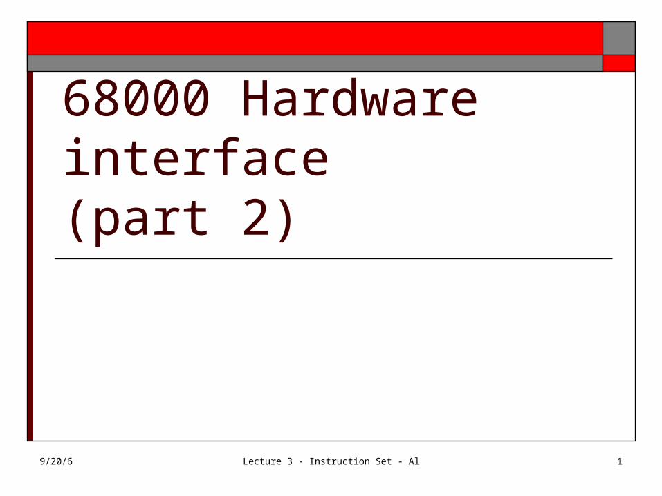
The 68000 Hardware Architecture - 2 Have gone over the all the pins except those
dealing with memory. Memory and Peripheral Interface Synchronous Bus Control Asynchronous Bus Control
9/20/6 Lecture 3 - Instruction Set - Al 3
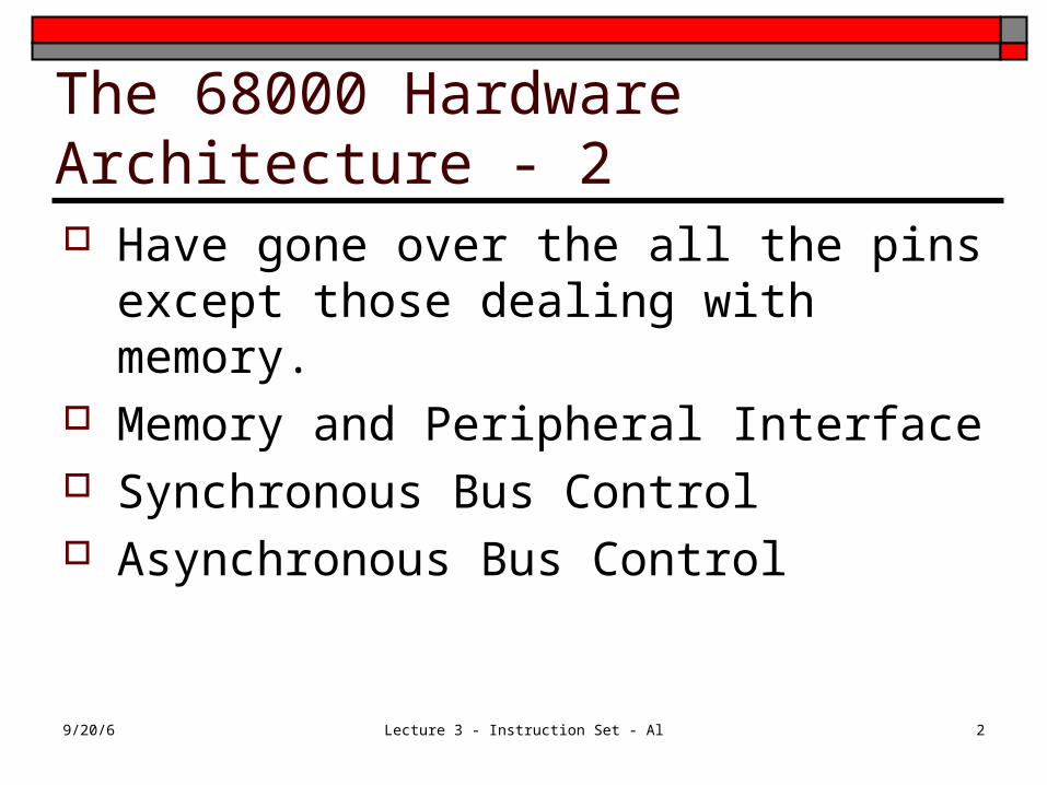
Memory and Peripheral Interface These pins take up 44 of the 64 pins Allow for reading from and writing to main
memory. The 68000 is a memory mapped architecture Memory Mapped Architecture
All input and output from the processor is to a single address space shared by memory and I/O ports. You need a memory map to know where the various activities are located.
9/20/6 Lecture 3 - Instruction Set - Al 4
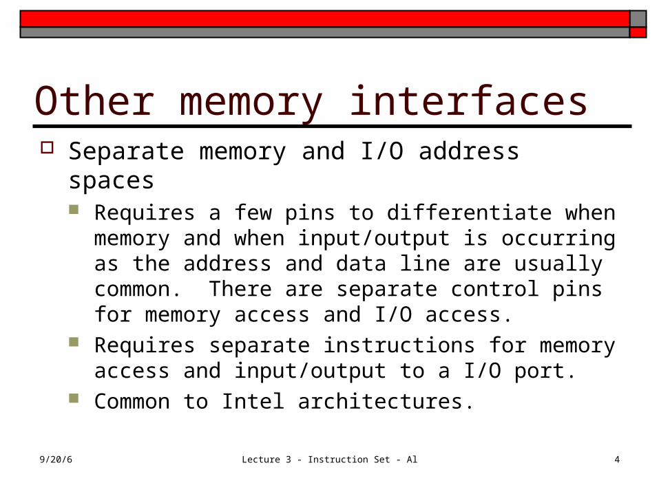
Other memory interfaces Separate memory and I/O address spaces
Requires a few pins to differentiate when memory and when input/output is occurring as the address and data line are usually common. There are separate control pins for memory access and I/O access.
Requires separate instructions for memory access and input/output to a I/O port.
Common to Intel architectures.
9/20/6 Lecture 3 - Instruction Set - Al 5
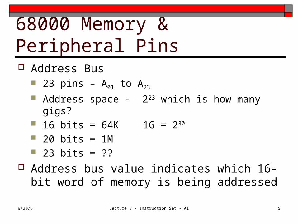
68000 Memory & Peripheral Pins Address Bus
23 pins – A01 to A23
Address space - 223 which is how many gigs? 16 bits = 64K 1G = 230
20 bits = 1M 23 bits = ??
Address bus value indicates which 16-bit word of memory is being addressed
9/20/6 Lecture 3 - Instruction Set - Al 6
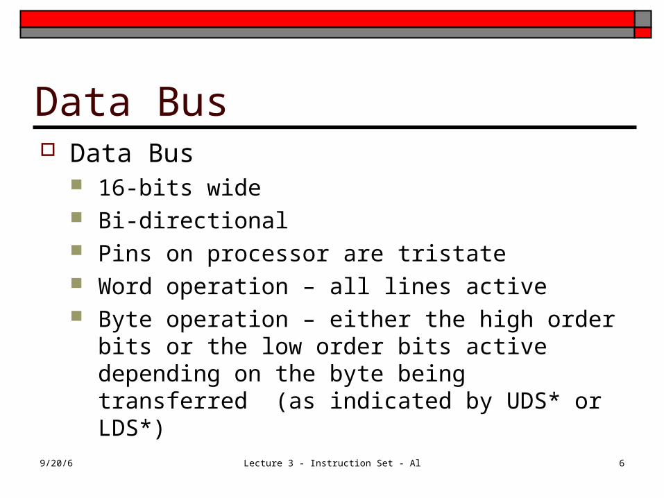
Data Bus Data Bus
16-bits wide Bi-directional Pins on processor are tristate Word operation – all lines active Byte operation – either the high order bits or the
low order bits active depending on the byte being transferred (as indicated by UDS* or LDS*)
9/20/6 Lecture 3 - Instruction Set - Al 7
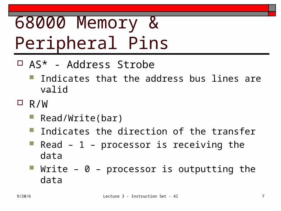
AS* - Address Strobe Indicates that the address bus lines are valid
R/W Read/Write(bar) Indicates the direction of the transfer Read – 1 – processor is receiving the data Write – 0 – processor is outputting the data
68000 Memory & Peripheral Pins
9/20/6 Lecture 3 - Instruction Set - Al 8
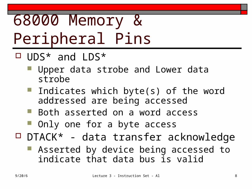
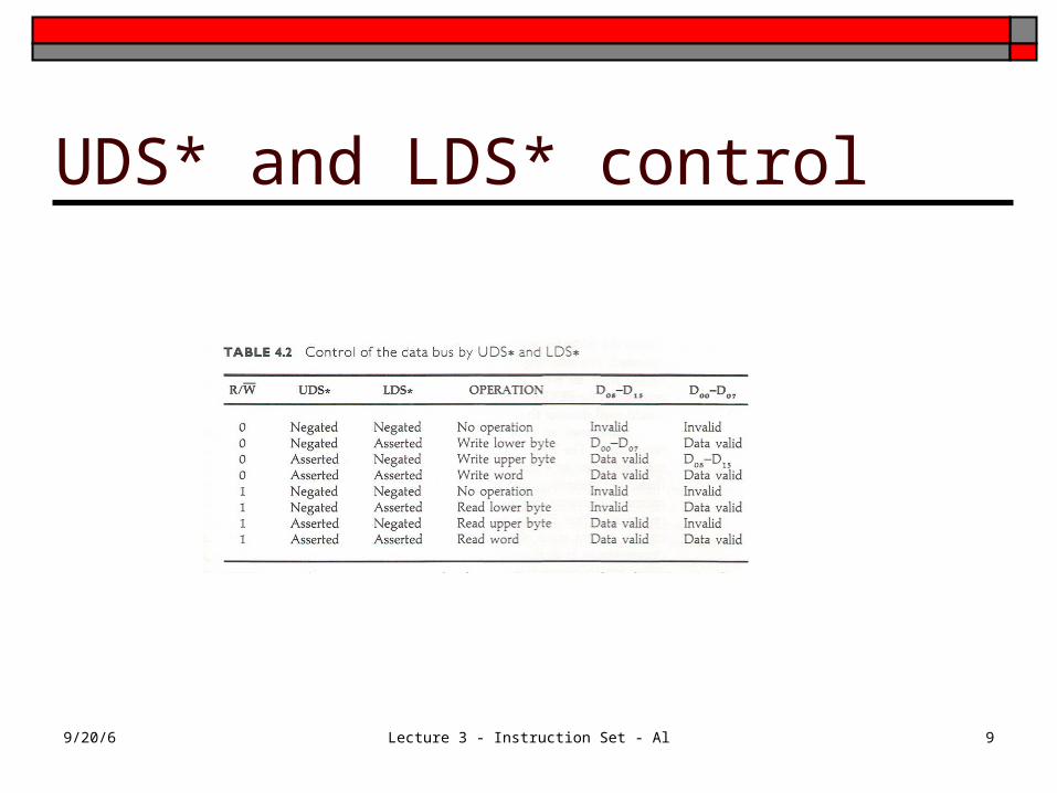
68000 Memory & Peripheral Pins UDS* and LDS*
Upper data strobe and Lower data strobe Indicates which byte(s) of the word addressed are
being accessed Both asserted on a word access Only one for a byte access
DTACK* - data transfer acknowledge Asserted by device being accessed to indicate that
data bus is valid
9/20/6 Lecture 3 - Instruction Set - Al 9
UDS* and LDS* control
9/20/6 Lecture 3 - Instruction Set - Al 10
Synchronous Bus Control Most transfers take place asynchronously 3 pins for synchronous bus control
VPA* - Valid peripheral address VMA* - Valid memory address E – Enable output from the 68000 – A timing
signal for interfacing with 6800 series peripherals
9/20/6 Lecture 3 - Instruction Set - Al 11
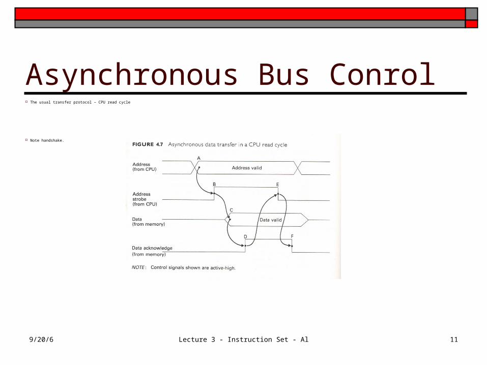
Asynchronous Bus Conrol The usual transfer protocol – CPU read cycle
Note handshake.
9/20/6 Lecture 3 - Instruction Set - Al 12
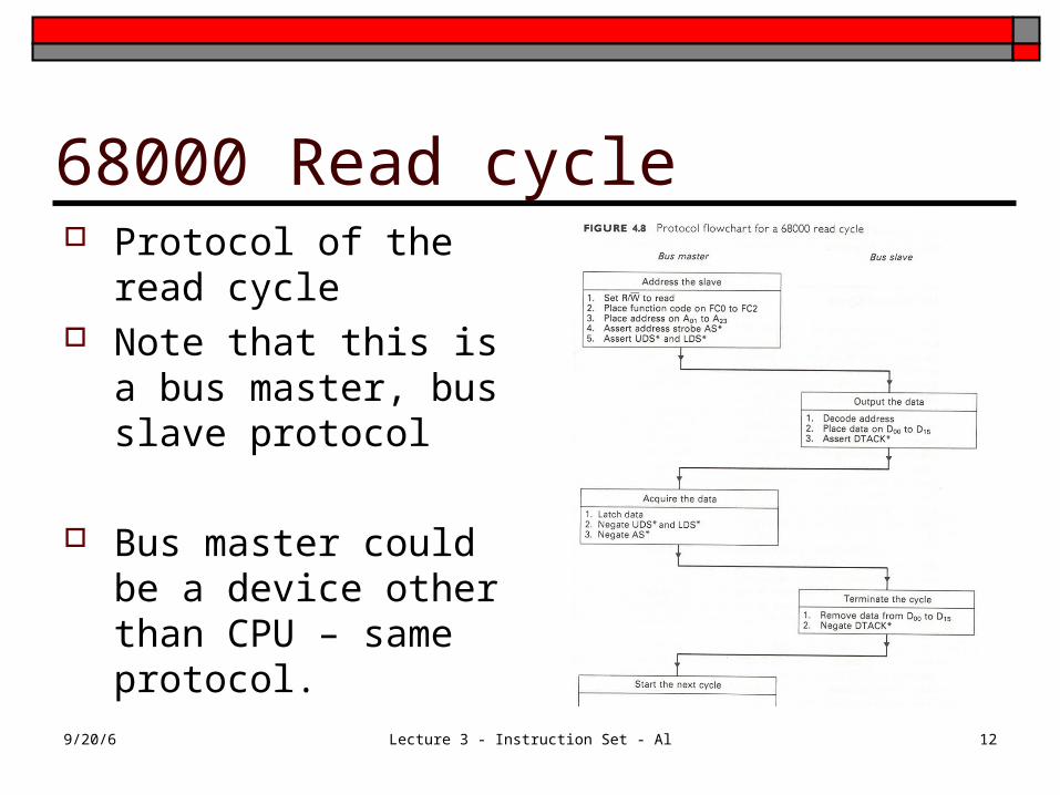
68000 Read cycle Protocol of the read
cycle Note that this is a bus
master, bus slave protocol
Bus master could be a device other than CPU – same protocol.
9/20/6 Lecture 3 - Instruction Set - Al 13
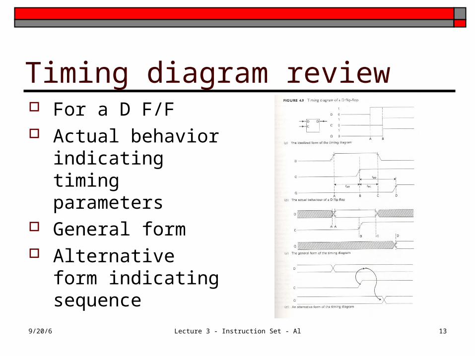
Timing diagram review For a D F/F Actual behavior
indicating timing parameters
General form Alternative form
indicating sequence
9/20/6 Lecture 3 - Instruction Set - Al 14
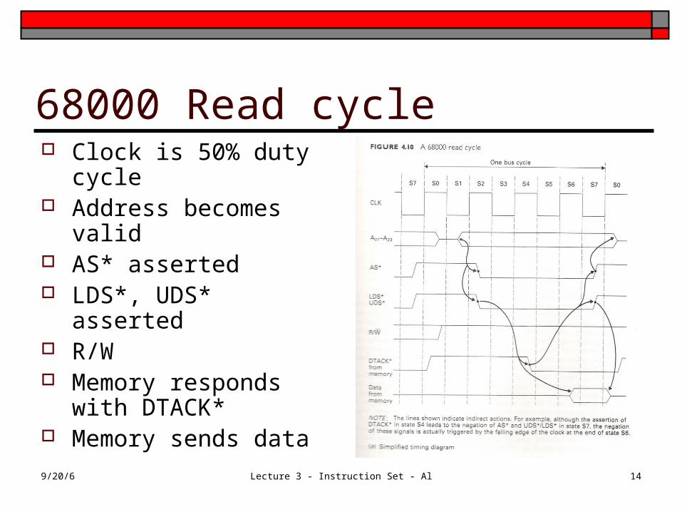
68000 Read cycle Clock is 50% duty
cycle Address becomes valid AS* asserted LDS*, UDS* asserted R/W Memory responds with
DTACK* Memory sends data
9/20/6 Lecture 3 - Instruction Set - Al 15
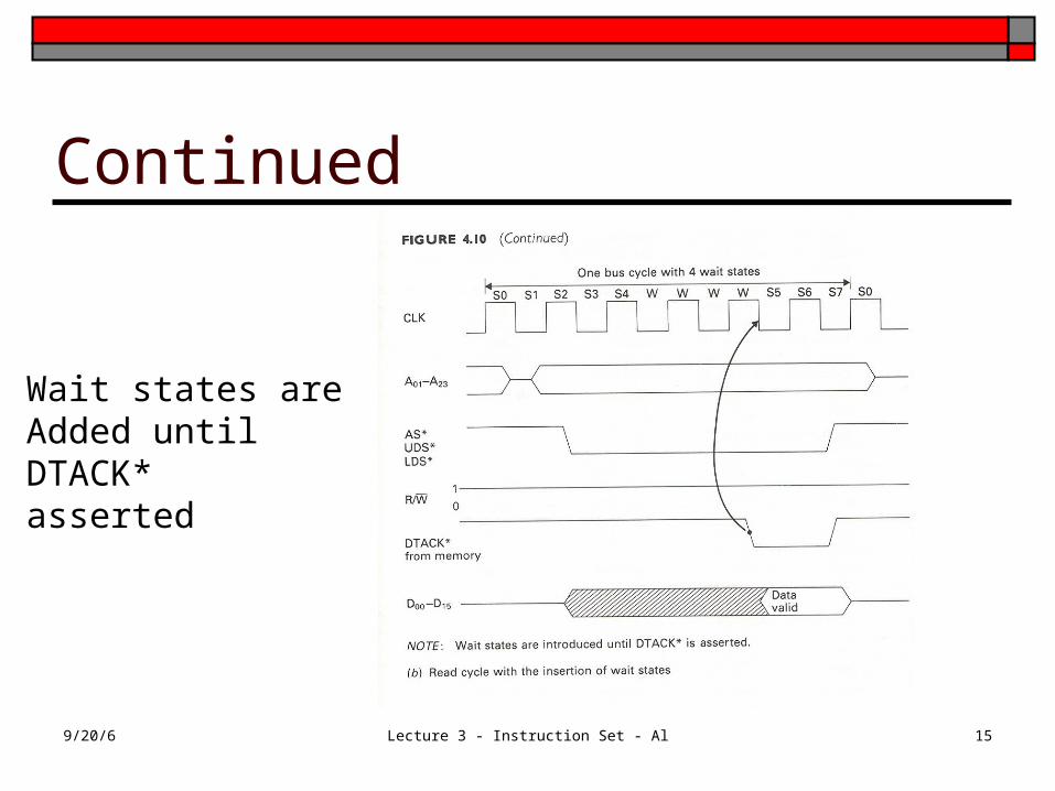
Continued
Wait states areAdded until DTACK*asserted
9/20/6 Lecture 3 - Instruction Set - Al 16
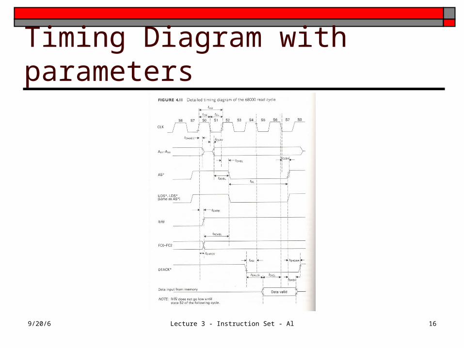
Timing Diagram with parameters
9/20/6 Lecture 3 - Instruction Set - Al 17
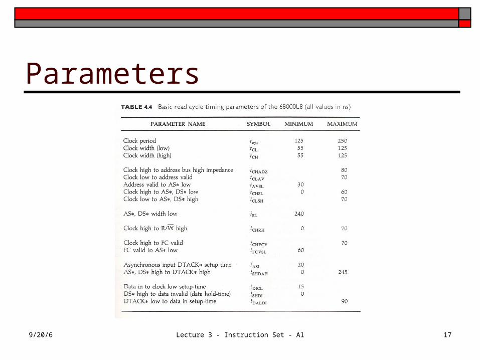
Parameters
9/20/6 Lecture 3 - Instruction Set - Al 18
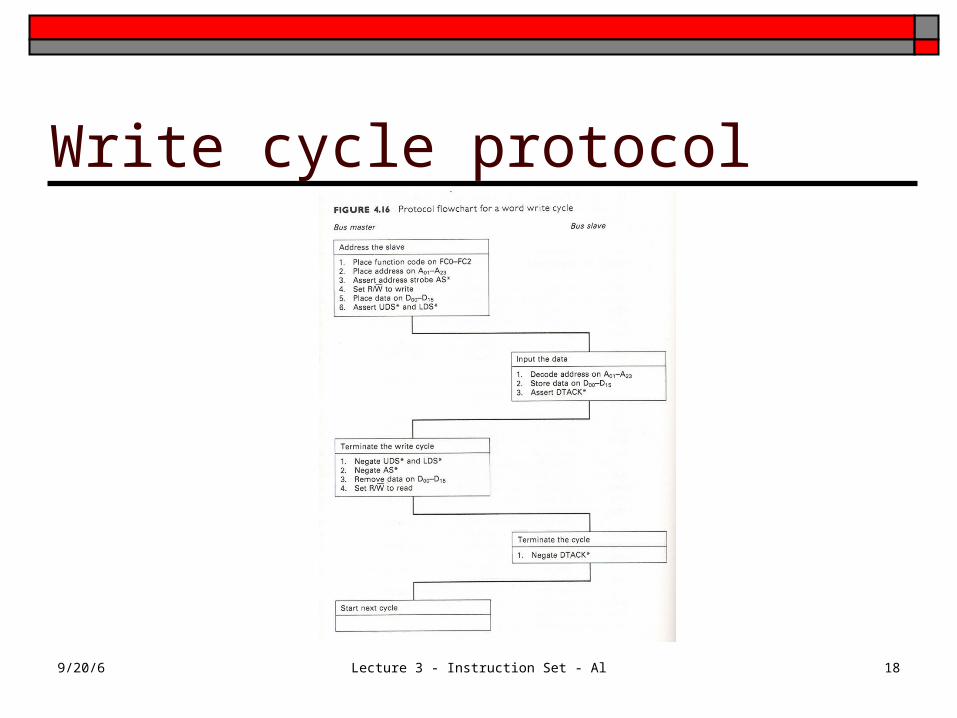
Write cycle protocol
9/20/6 Lecture 3 - Instruction Set - Al 19
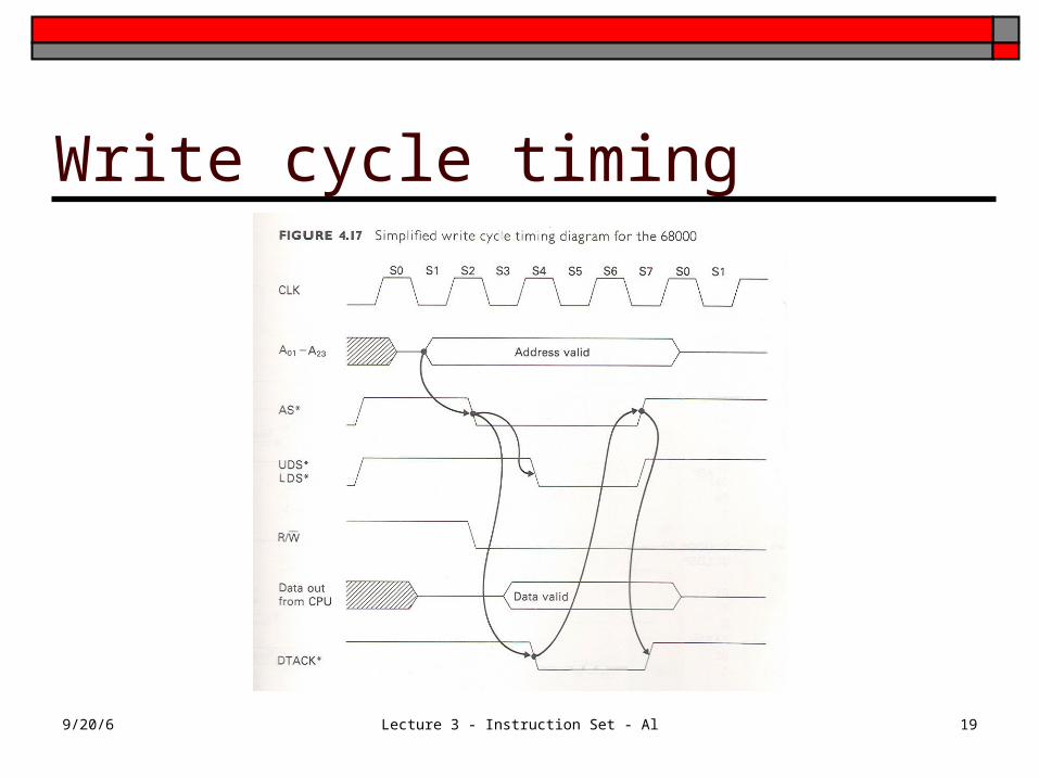
Write cycle timing
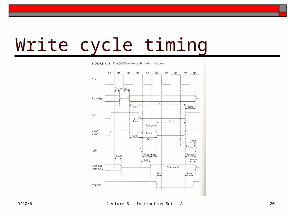
9/20/6 Lecture 3 - Instruction Set - Al 20
Write cycle timing
9/20/6 Lecture 3 - Instruction Set - Al 21
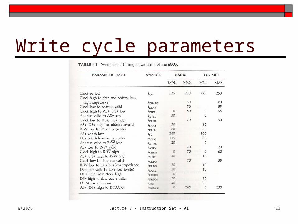
Write cycle parameters