87LPC764 Low power, low price, low pin count (20 pin ... · PDF file87LPC764 Low power, low...
54
Philips Semiconductors 87LPC764 Low power, low price, low pin count (20 pin) microcontroller with 4 kB OTP Preliminary specification Supersedes data of 1999 Aug 27 IC28 Data Handbook 1999 Dec 21 INTEGRATED CIRCUITS
Transcript of 87LPC764 Low power, low price, low pin count (20 pin ... · PDF file87LPC764 Low power, low...

������ ����������
87LPC764Low power, low price, low pin count(20 pin) microcontroller with 4 kB OTP
Preliminary specificationSupersedes data of 1999 Aug 27IC28 Data Handbook
1999 Dec 21
INTEGRATED CIRCUITS

Philips Semiconductors Preliminary specification
87LPC764Low power, low price, low pin count (20 pin)microcontroller with 4 kB OTP
21999 Dec 21
TABLE OF CONTENTS
General Description 3. . . . . . . . . . . . . . . . . . . . . . . . Features 3. . . . . . . . . . . . . . . . . . . . . . . . . . . . . . . . . . . . . . . . . . . . .
Ordering Information 4. . . . . . . . . . . . . . . . . . . . . . . Pin Configuration,20-Pin DIP and SO Packages 4. . . . . . . . . . . . . . . Logic Symbol 4. . . . . . . . . . . . . . . . . . . . . . . . . . . . . Block Diagram 5. . . . . . . . . . . . . . . . . . . . . . . . . . . . . Pin Descriptions 7. . . . . . . . . . . . . . . . . . . . . . . . . . . Special Function Registers 8. . . . . . . . . . . . . . . . . Functional Description 10. . . . . . . . . . . . . . . . . . . . .
Enhanced CPU 10. . . . . . . . . . . . . . . . . . . . . . . . . . . . . . . . . . . . . . . Analog Functions 10. . . . . . . . . . . . . . . . . . . . . . . . . . . . . . . . . . . . . Analog Comparators 10. . . . . . . . . . . . . . . . . . . . . . . . . . . . . . . . . .
Comparator Configuration 10. . . . . . . . . . . . . . . . . . . . . . . . . . Internal Reference Voltage 12. . . . . . . . . . . . . . . . . . . . . . . . . Comparator Interrupt 12. . . . . . . . . . . . . . . . . . . . . . . . . . . . . . Comparators and Power Reduction Modes 12. . . . . . . . . . . Comparator Configuration Example 12. . . . . . . . . . . . . . . . . .
I2C Serial Interface 13. . . . . . . . . . . . . . . . . . . . . . . . . . . . . . . . . . . . I2C Interrupts 13. . . . . . . . . . . . . . . . . . . . . . . . . . . . . . . . . . . . . Reading I2CON 13. . . . . . . . . . . . . . . . . . . . . . . . . . . . . . . . . . . Checking ATN and DRDY 15. . . . . . . . . . . . . . . . . . . . . . . . . . Writing I2CON 15. . . . . . . . . . . . . . . . . . . . . . . . . . . . . . . . . . . . Regarding Transmit Active 15. . . . . . . . . . . . . . . . . . . . . . . . . Regarding Software Response Time 16. . . . . . . . . . . . . . . . .
Interrupts 17. . . . . . . . . . . . . . . . . . . . . . . . . . . . . . . . . . . . . . . . . . . . External Interrupt Inputs 18. . . . . . . . . . . . . . . . . . . . . . . . . . . .
I/O Ports 19. . . . . . . . . . . . . . . . . . . . . . . . . . . . . . . . . . . . . . . . . . . . Quasi–Bidirectional Output Configuration 19. . . . . . . . . . . . . Open Drain Output Configuration 20. . . . . . . . . . . . . . . . . . . . Push–Pull Output Configuration 20. . . . . . . . . . . . . . . . . . . . .
Keyboard Interrupt (KBI) 21. . . . . . . . . . . . . . . . . . . . . . . . . . . . . . . Oscillator 24. . . . . . . . . . . . . . . . . . . . . . . . . . . . . . . . . . . . . . . . . . . .
Low Speed Oscillator Option 24. . . . . . . . . . . . . . . . . . . . . . . . Medium Speed Oscillator Option 24. . . . . . . . . . . . . . . . . . . . High Speed Oscillator Option 24. . . . . . . . . . . . . . . . . . . . . . . On-Chip RC Oscillator Option 24. . . . . . . . . . . . . . . . . . . . . . . External Clock Input Option 24. . . . . . . . . . . . . . . . . . . . . . . . . Clock Output 24. . . . . . . . . . . . . . . . . . . . . . . . . . . . . . . . . . . . . CPU Clock Modification: CLKR and DIVM 25. . . . . . . . . . . .
Power Monitoring Functions 25. . . . . . . . . . . . . . . . . . . . . . . . . . . . Brownout Detection 25. . . . . . . . . . . . . . . . . . . . . . . . . . . . . . . Power On Detection 26. . . . . . . . . . . . . . . . . . . . . . . . . . . . . . .
Power Reduction Modes 26. . . . . . . . . . . . . . . . . . . . . . . . . . . . . . . Idle Mode 26. . . . . . . . . . . . . . . . . . . . . . . . . . . . . . . . . . . . . . . . Power Down Mode 26. . . . . . . . . . . . . . . . . . . . . . . . . . . . . . . . Low Voltage EPROM Operation 28. . . . . . . . . . . . . . . . . . . . .
Reset 28. . . . . . . . . . . . . . . . . . . . . . . . . . . . . . . . . . . . . . . . . . . . . . . Timer/Counters 29. . . . . . . . . . . . . . . . . . . . . . . . . . . . . . . . . . . . . . .
Mode 0 30. . . . . . . . . . . . . . . . . . . . . . . . . . . . . . . . . . . . . . . . . . Mode 1 31. . . . . . . . . . . . . . . . . . . . . . . . . . . . . . . . . . . . . . . . . . Mode 2 31. . . . . . . . . . . . . . . . . . . . . . . . . . . . . . . . . . . . . . . . . . Mode 3 31. . . . . . . . . . . . . . . . . . . . . . . . . . . . . . . . . . . . . . . . . . Timer Overflow Toggle Output 32. . . . . . . . . . . . . . . . . . . . . .
UART 32. . . . . . . . . . . . . . . . . . . . . . . . . . . . . . . . . . . . . . . . . . . . . . . Mode 0 32. . . . . . . . . . . . . . . . . . . . . . . . . . . . . . . . . . . . . . . . . . Mode 1 32. . . . . . . . . . . . . . . . . . . . . . . . . . . . . . . . . . . . . . . . . . Mode 2 32. . . . . . . . . . . . . . . . . . . . . . . . . . . . . . . . . . . . . . . . . . Mode 3 32. . . . . . . . . . . . . . . . . . . . . . . . . . . . . . . . . . . . . . . . . . Serial Port Control Register (SCON) 33. . . . . . . . . . . . . . . . . Baud Rates 34. . . . . . . . . . . . . . . . . . . . . . . . . . . . . . . . . . . . . . Using Timer 1 to Generate Baud Rates 34. . . . . . . . . . . . . . More About UART Mode 0 36. . . . . . . . . . . . . . . . . . . . . . . . . More About UART Mode 1 36. . . . . . . . . . . . . . . . . . . . . . . . . More About UART Modes 2 and 3 39. . . . . . . . . . . . . . . . . . . Multiprocessor Communications 39. . . . . . . . . . . . . . . . . . . . Automatic Address Recognition 42. . . . . . . . . . . . . . . . . . . . .
Watchdog Timer 42. . . . . . . . . . . . . . . . . . . . . . . . . . . . . . . . . . . . . . Watchdog Feed Sequence 42. . . . . . . . . . . . . . . . . . . . . . . . . Watchdog Reset 42. . . . . . . . . . . . . . . . . . . . . . . . . . . . . . . . . .
Additional Features 44. . . . . . . . . . . . . . . . . . . . . . . . . . . . . . . . . . . Software Reset 44. . . . . . . . . . . . . . . . . . . . . . . . . . . . . . . . . . . Dual Data Pointers 44. . . . . . . . . . . . . . . . . . . . . . . . . . . . . . . .
EPROM Characteristics 45. . . . . . . . . . . . . . . . . . . . . . . . . . . . . . . System Configuration Bytes 45. . . . . . . . . . . . . . . . . . . . . . . . Security Bits 46. . . . . . . . . . . . . . . . . . . . . . . . . . . . . . . . . . . . . .
Absolute Maximum Ratings 46. . . . . . . . . . . . . . . . . DC Electrical Characteristics 47. . . . . . . . . . . . . . . . Comparator Electrical Characteristics 48. . . . . . . AC Electrical Characteristics 48. . . . . . . . . . . . . . . .

Philips Semiconductors Preliminary specification
87LPC764Low power, low price, low pin count (20 pin)microcontroller with 4 kB OTP
1999 Dec 21 3
GENERAL DESCRIPTIONThe 87LPC764 is a 20-pin single-chip microcontroller designed forlow pin count applications demanding high-integration, low costsolutions over a wide range of performance requirements. Amember of the Philips low pin count family, the 87LPC764 offersprogrammable oscillator configurations for high and low speedcrystals or RC operation, wide operating voltage range,programmable port output configurations, selectable Schmitt triggerinputs, LED drive outputs, and a built-in watchdog timer. The87LPC764 is based on an accelerated 80C51 processorarchitecture that executes instructions at twice the rate of standard80C51 devices.
FEATURES• An accelerated 80C51 CPU provides instruction cycle times of
300–600 ns for all instructions except multiply and divide whenexecuting at 20 MHz. Execution at up to 20 MHz whenVDD = 4.5 V to 6.0 V, 10 MHz when VDD = 2.7 V to 6.0 V.
• 2.7 V to 6.0 V operating range for digital functions.
• 4 K bytes EPROM code memory.
• 128 byte RAM data memory.
• 32-byte customer code EPROM allows serialization of devices,storage of setup parameters, etc.
• Two 16-bit counter/timers. Each timer may be configured to togglea port output upon timer overflow.
• Two analog comparators.
• Full duplex UART.
• I2C communication port.
• Eight keypad interrupt inputs, plus two additional external interruptinputs.
• Four interrupt priority levels.
• Watchdog timer with separate on-chip oscillator, requiring noexternal components. The watchdog timeout time is selectablefrom 8 values.
• Active low reset. On-chip power-on reset allows operation with noexternal reset components.
• Low voltage reset. One of two preset low voltage levels may beselected to allow a graceful system shutdown when power fails.May optionally be configured as an interrupt.
• Oscillator Fail Detect. The watchdog timer has a separate fullyon-chip oscillator, allowing it to perform an oscillator fail detectfunction.
• Configurable on-chip oscillator with frequency range and RCoscillator options (selected by user programmed EPROM bits).The RC oscillator option allows operation with no externaloscillator components.
• Programmable port output configuration options:quasi-bidirectional, open drain, push-pull, input-only.
• Selectable Schmitt trigger port inputs.
• LED drive capability (20 mA) on all port pins.
• Controlled slew rate port outputs to reduce EMI. Outputs haveapproximately 10 ns minimum ramp times.
• 15 I/O pins minimum. Up to 18 I/O pins using on-chip oscillatorand reset options.
• Only power and ground connections are required to operate the87LPC764 when fully on-chip oscillator and reset options areselected.
• Serial EPROM programming allows simple in-circuit productioncoding. Two EPROM security bits prevent reading of sensitiveapplication programs.
• Idle and Power Down reduced power modes. Improved wakeupfrom Power Down mode (a low interrupt input starts execution).Typical Power Down current is 1 m A.
• 20-pin DIP and SO packages.

Philips Semiconductors Preliminary specification
87LPC764Low power, low price, low pin count (20 pin)microcontroller with 4 kB OTP
1999 Dec 21 4
ORDERING INFORMATION
Part Number Temperature Range °C and Package Frequency Drawing Number
P87LPC764B N 0 to +70, Plastic Dual In-Line Package 20 MHz (5 V), 10 MHz (3 V) SOT146–1
P87LPC764B D 0 to +70, Plastic Small Outline Package 20 MHz (5 V), 10 MHz (3 V) SOT163–1
P87LPC764F N –45 to +85, Plastic Dual In-Line Package 20 MHz (5 V), 10 MHz (3 V) SOT146–1
P87LPC764F D –45 to +85, Plastic Small Outline Package 20 MHz (5 V), 10 MHz (3 V) SOT163–1
PIN CONFIGURATION, 20-PIN DIP AND SO PACKAGES
SU01149
1
2
3
4
5
6
7
8
9
11
12
13
14
15
16
17
18
19
20CMP2/P0.0
P1.7
P1.6
RST/P1.5
VSS
X1/P2.1
X2/CLKOUT/P2.0
INT1/P1.4
SDA/INT0/P1.3
SCL/T0/P1.2
P0.1/CIN2B
P0.2/CIN2A
P0.3/CIN1B
P0.4/CIN1A
P0.5/CMPREF
VDD
P0.6/CMP1
P1.0/TxD
P0.7/T1
P1.1/RxD10
LOGIC SYMBOL
T1
X1
SU01150
VDD VSS
TxDCMP2
CIN2B
CIN2A
CIN1B
CIN1A
CMPREF
CMP1
CLKOUT/X2
PO
RT
0P
OR
T 2
PO
RT
1
RxD
INT0
RST
INT1
T0 SCL
SDA

Philips Semiconductors Preliminary specification
87LPC764Low power, low price, low pin count (20 pin)microcontroller with 4 kB OTP
1999 Dec 21 5
BLOCK DIAGRAM
SU01151
TIMER 0, 1
I2C
UART
ACCELERATED80C51 CPU
WATCHDOG TIMERAND OSCILLATOR
PORT 0CONFIGURABLE I/OS
128 BYTEDATA RAM
4K BYTE CODE EPROM
INTERNAL BUS
ANALOGCOMPARATORS
PORT 1CONFIGURABLE I/OS
KEYPADINTERRUPT
PORT 2CONFIGURABLE I/OS
POWER MONITOR(POWER-ON RESET,BROWNOUT RESET)
CONFIGURABLEOSCILLATOR
CRYSTAL ORRESONATOR
ON-CHIPR/C
OSCILLATOR

Philips Semiconductors Preliminary specification
87LPC764Low power, low price, low pin count (20 pin)microcontroller with 4 kB OTP
1999 Dec 21 6
SU01216
UNUSED CODEMEMORY SPACE
32-BYTE CUSTOMERCODE SPACE
(ACCESSIBLE VIA MOVC)
UNUSED CODEMEMORY SPACE
4 K BYTES ON-CHIPCODE MEMORY
INTERRUPT VECTORS
SPECIAL FUNCTIONREGISTERS
(ONLY DIRECTLYADDRESSABLE)
128 BYTES ON-CHIP DATAMEMORY
(DIRECTLY ANDINDIRECTLY
ADDRESSABLE)
16-BIT ADDRESSABLE BYTES
UNUSED SPACE
CONFIGURATION BYTESUCFG1, UCFG2
(ACCESSIBLE VIA MOVX)
UNUSED SPACE
FFFFh
FCFFh
FCE0h
1000h0FFFh
FFh
80h7Fh
0000h 00h 0000h
FD00h
FD01h
FFFFh
* The 87LPC764 does not support access to external data memory. However, the User Configuration Bytes are accessed via the MOVX instruction as if they were in external data memory.
ON-CHIP CODEMEMORY SPACE
ON-CHIP DATAMEMORY SPACE
EXTERNAL DATAMEMORY SPACE*
Figure 1. 87LPC764 Program and Data Memory Map

Philips Semiconductors Preliminary specification
87LPC764Low power, low price, low pin count (20 pin)microcontroller with 4 kB OTP
1999 Dec 21 7
PIN DESCRIPTIONSMNEMONIC PIN NO. TYPE NAME AND FUNCTION
P0.0–P0.7 1, 13, 14,16–20
I/O Port 0 : Port 0 is an 8-bit I/O port with a user-configurable output type. Port 0 latches are configured inthe quasi-bidirectional mode and have either ones or zeros written to them during reset, as determinedby the PRHI bit in the UCFG1 configuration byte. The operation of port 0 pins as inputs and outputsdepends upon the port configuration selected. Each port pin is configured independently. Refer to thesection on I/O port configuration and the DC Electrical Characteristics for details.
The Keyboard Interrupt feature operates with port 0 pins.
Port 0 also provides various special functions as described below.
1 O P0.0 CMP2 Comparator 2 output.
20 I P0.1 CIN2B Comparator 2 positive input B.
19 I P0.2 CIN2A Comparator 2 positive input A.
18 I P0.3 CIN1B Comparator 1 positive input B.
17 I P0.4 CIN1A Comparator 1 positive input A.
16 I P0.5 CMPREF Comparator reference (negative) input.
14 O P0.6 CMP1 Comparator 1 output.
13 I/O P0.7 T1 Timer/counter 1 external count input or overflow output.
P1.0–P1.7 2–4, 8–12 I/O Port 1 : Port 1 is an 8-bit I/O port with a user-configurable output type, except for three pins as notedbelow. Port 1 latches are configured in the quasi-bidirectional mode and have either ones or zeroswritten to them during reset, as determined by the PRHI bit in the UCFG1 configuration byte. Theoperation of the configurable port 1 pins as inputs and outputs depends upon the port configurationselected. Each of the configurable port pins are programmed independently. Refer to the section on I/Oport configuration and the DC Electrical Characteristics for details.
Port 1 also provides various special functions as described below.
12 O P1.0 TxD Transmitter output for the serial port.
11 I P1.1 RxD Receiver input for the serial port.
10 I/O
I/O
P1.2 T0 Timer/counter 0 external count input or overflow output.
SCL I2C serial clock input/output. When configured as an output, P1.2 is opendrain, in order to conform to I2C specifications.
9 I
I/O
P1.3 INT0 External interrupt 0 input.
SDA I2C serial data input/output. When configured as an output, P1.3 is opendrain, in order to conform to I2C specifications.
8 I P1.4 INT1 External interrupt 1 input.
4 I P1.5 RST External Reset input (if selected via EPROM configuration). A low on this pinresets the microcontroller, causing I/O ports and peripherals to take on theirdefault states, and the processor begins execution at address 0. When usedas a port pin, P1.5 is a Schmitt trigger input only.
P2.0–P2.1 6, 7 I/O Port 2 : Port 2 is a 2-bit I/O port with a user-configurable output type. Port 2 latches are configured in thequasi-bidirectional mode and have either ones or zeros written to them during reset, as determined bythe PRHI bit in the UCFG1 configuration byte. The operation of port 2 pins as inputs and outputsdepends upon the port configuration selected. Each port pin is configured independently. Refer to thesection on I/O port configuration and the DC Electrical Characteristics for details.
Port 2 also provides various special functions as described below.
7 O P2.0 X2 Output from the oscillator amplifier (when a crystal oscillator option isselected via the EPROM configuration).
CLKOUT CPU clock divided by 6 clock output when enabled via SFR bit and inconjunction with internal RC oscillator or external clock input.
6 I P2.1 X1 Input to the oscillator circuit and internal clock generator circuits (whenselected via the EPROM configuration).
VSS 5 I Ground : 0V reference.
VDD 15 I Power Supply : This is the power supply voltage for normal operation as well as Idle andPower Down modes.

Philips Semiconductors Preliminary specification
87LPC764Low power, low price, low pin count (20 pin)microcontroller with 4 kB OTP
1999 Dec 21 8
SPECIAL FUNCTION REGISTERS
Name Description SFRAddress
Bit Functions and AddressesMSB LSB
ResetValue
E7 E6 E5 E4 E3 E2 E1 E0
ACC* Accumulator E0h 00h
AUXR1# Auxiliary Function Register A2h KBF BOD BOI LPEP SRST 0 – DPS 02h1
F7 F6 F5 F4 F3 F2 F1 F0
B* B register F0h 00h
CMP1# Comparator 1 controlregister ACh – – CE1 CP1 CN1 OE1 CO1 CMF1 00h1
CMP2# Comparator 2 controlregister ADh – – CE2 CP2 CN2 OE2 CO2 CMF2 00h1
DIVM# CPU clock divide-by-Mcontrol 95h 00h
DPTR: Data pointer (2 bytes) DPH Data pointer high byte 83h 00h DPL Data pointer low byte 82h 00h
CF CE CD CC CB CA C9 C8
I2CFG#* I2C configuration register C8h/RD SLAVEN MASTRQ 0 TIRUN – – CT1 CT0 00h1
C8h/WR SLAVEN MASTRQ CLRTI TIRUN – – CT1 CT0
DF DE DD DC DB DA D9 D8
I2CON#* I2C control register D8h/RD RDAT ATN DRDY ARL STR STP MASTER – 80h1
D8h/WR CXA IDLE CDR CARL CSTR CSTP XSTR XSTP
I2DAT# I2C data register D9h/RD RDAT 0 0 0 0 0 0 0 80h
D9h/WR XDAT x x x x x x x
AF AE AD AC AB AA A9 A8
IEN0* Interrupt enable 0 A8h EA EWD EBO ES ET1 EX1 ET0 EX0 00h
EF EE ED EC EB EA E9 E8
IEN1#* Interrupt enable 1 E8h ETI – EC1 – – EC2 EKB EI2 00h1
BF BE BD BC BB BA B9 B8
IP0* Interrupt priority 0 B8h – PWD PBO PS PT1 PX1 PT0 PX0 00h1
IP0H# Interrupt priority 0 high byte B7h – PWDH PBOH PSH PT1H PX1H PT0H PX0H 00h1
FF FE FD FC FB FA F9 F8
IP1* Interrupt priority 1 F8h PTI – PC1 – – PC2 PKB PI2 00h1
IP1H# Interrupt priority 1 high byte F7h PTIH – PC1H – – PC2H PKBH PI2H 00h1
KBI# Keyboard Interrupt 86h 00h
87 86 85 84 83 82 81 80
P0* Port 0 80h T1 CMP1 CMPREF CIN1A CIN1B CIN2A CIN2B CMP2 Note 2
97 96 95 94 93 92 91 90
P1* Port 1 90h (P1.7) (P1.6) RST INT1 INT0 T0 RxD TxD Note 2
A7 A6 A5 A4 A3 A2 A1 A0
P2* Port 2 A0h – – – – – – X1 X2 Note 2
P0M1# Port 0 output mode 1 84h (P0M1.7) (P0M1.6) (P0M1.5) (P0M1.4) (P0M1.3) (P0M1.2) (P0M1.1) (P0M1.0) 00h
P0M2# Port 0 output mode 2 85h (P0M2.7) (P0M2.6) (P0M2.5) (P0M2.4) (P0M2.3) (P0M2.2) (P0M2.1) (P0M2.0) 00H
P1M1# Port 1 output mode 1 91h (P1M1.7) (P1M1.6) – (P1M1.4) – – (P1M1.1) (P1M1.0) 00h1
P1M2# Port 1 output mode 2 92h (P1M2.7) (P1M2.6) – (P1M2.4) – – (P1M2.1) (P1M2.0) 00h1
P2M1# Port 2 output mode 1 A4h P2S P1S P0S ENCLK ENT1 ENT0 (P2M1.1) (P2M1.0) 00h
P2M2# Port 2 output mode 2 A5h – – – – – – (P2M2.1) (P2M2.0) 00h1
PCON Power control register 87h SMOD1 SMOD0 BOF POF GF1 GF0 PD IDL Note 3

Philips Semiconductors Preliminary specification
87LPC764Low power, low price, low pin count (20 pin)microcontroller with 4 kB OTP
1999 Dec 21 9
NameResetValue
Bit Functions and AddressesMSB LSB
SFRAddressDescription
D7 D6 D5 D4 D3 D2 D1 D0
PSW* Program status word D0h CY AC F0 RS1 RS0 OV F1 P 00h
PT0AD# Port 0 digital input disable F6h 00h
9F 9E 9D 9C 9B 9A 99 98
SCON* Serial port control 98h SM0 SM1 SM2 REN TB8 RB8 TI RI 00h
SBUF Serial port data bufferregister 99h xxh
SADDR# Serial port address register A9h 00h
SADEN# Serial port address enable B9h 00h
SP Stack pointer 81h 07h
8F 8E 8D 8C 8B 8A 89 88
TCON* Timer 0 and 1 control 88h TF1 TR1 TF0 TR0 IE1 IT1 IE0 IT0 00h
TH0 Timer 0 high byte 8Ch 00h
TH1 Timer 1 high byte 8Dh 00h
TL0 Timer 0 low byte 8Ah 00h
TL1 Timer 1 low byte 8Bh 00h
TMOD Timer 0 and 1 mode 89h GATE C/T M1 M0 GATE C/T M1 M0 00h
WDCON# Watchdog control register A7h – – WDOVF WDRUN WDCLK WDS2 WDS1 WDS0 Note 4
WDRST# Watchdog reset register A6h xxh
NOTES:* SFRs are bit addressable.# SFRs are modified from or added to the 80C51 SFRs.1. Unimplemented bits in SFRs are X (unknown) at all times. Ones should not be written to these bits since they may be used for other
purposes in future derivatives. The reset value shown in the table for these bits is 0.2. I/O port values at reset are determined by the PRHI bit in the UCFG1 configuration byte.3. The PCON reset value is x x BOF POF–0 0 0 0b. The BOF and POF flags are not affected by reset. The POF flag is set by hardware upon
power up. The BOF flag is set by the occurrence of a brownout reset/interrupt and upon power up.4. The WDCON reset value is xx11 0000b for a Watchdog reset, xx01 0000b for all other reset causes if the watchdog is enabled, and xx00
0000b for all other reset causes if the watchdog is disabled.
Philips Semiconductors Preliminary specification
87LPC764Low power, low price, low pin count (20 pin)microcontroller with 4 kB OTP
1999 Dec 21 10
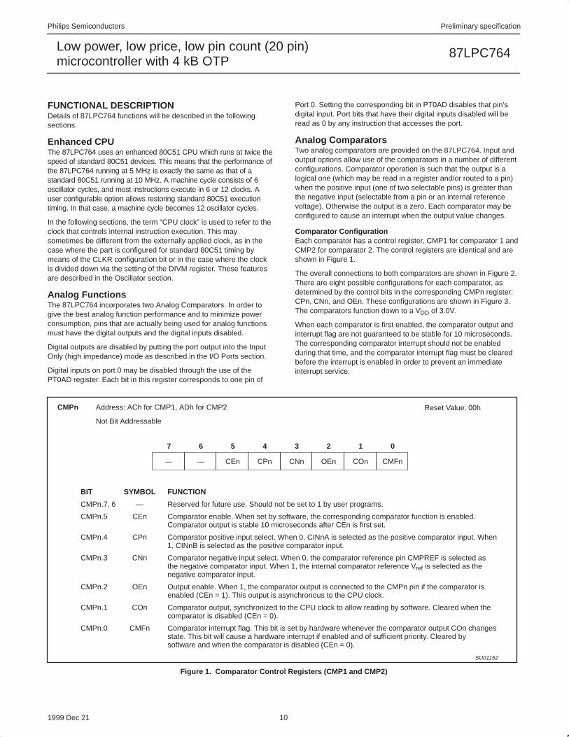
FUNCTIONAL DESCRIPTIONDetails of 87LPC764 functions will be described in the followingsections.
Enhanced CPUThe 87LPC764 uses an enhanced 80C51 CPU which runs at twice thespeed of standard 80C51 devices. This means that the performance ofthe 87LPC764 running at 5 MHz is exactly the same as that of astandard 80C51 running at 10 MHz. A machine cycle consists of 6oscillator cycles, and most instructions execute in 6 or 12 clocks. Auser configurable option allows restoring standard 80C51 executiontiming. In that case, a machine cycle becomes 12 oscillator cycles.
In the following sections, the term “CPU clock” is used to refer to theclock that controls internal instruction execution. This maysometimes be different from the externally applied clock, as in thecase where the part is configured for standard 80C51 timing bymeans of the CLKR configuration bit or in the case where the clockis divided down via the setting of the DIVM register. These featuresare described in the Oscillator section.
Analog FunctionsThe 87LPC764 incorporates two Analog Comparators. In order togive the best analog function performance and to minimize powerconsumption, pins that are actually being used for analog functionsmust have the digital outputs and the digital inputs disabled.
Digital outputs are disabled by putting the port output into the InputOnly (high impedance) mode as described in the I/O Ports section.
Digital inputs on port 0 may be disabled through the use of thePT0AD register. Each bit in this register corresponds to one pin of
Port 0. Setting the corresponding bit in PT0AD disables that pin’sdigital input. Port bits that have their digital inputs disabled will beread as 0 by any instruction that accesses the port.
Analog ComparatorsTwo analog comparators are provided on the 87LPC764. Input andoutput options allow use of the comparators in a number of differentconfigurations. Comparator operation is such that the output is alogical one (which may be read in a register and/or routed to a pin)when the positive input (one of two selectable pins) is greater thanthe negative input (selectable from a pin or an internal referencevoltage). Otherwise the output is a zero. Each comparator may beconfigured to cause an interrupt when the output value changes.
Comparator ConfigurationEach comparator has a control register, CMP1 for comparator 1 andCMP2 for comparator 2. The control registers are identical and areshown in Figure 1.
The overall connections to both comparators are shown in Figure 2.There are eight possible configurations for each comparator, asdetermined by the control bits in the corresponding CMPn register:CPn, CNn, and OEn. These configurations are shown in Figure 3.The comparators function down to a VDD of 3.0V.
When each comparator is first enabled, the comparator output andinterrupt flag are not guaranteed to be stable for 10 microseconds.The corresponding comparator interrupt should not be enabledduring that time, and the comparator interrupt flag must be clearedbefore the interrupt is enabled in order to prevent an immediateinterrupt service.
BIT SYMBOL FUNCTION
CMPn.7, 6 — Reserved for future use. Should not be set to 1 by user programs.
CMPn.5 CEn Comparator enable. When set by software, the corresponding comparator function is enabled.Comparator output is stable 10 microseconds after CEn is first set.
CMPn.4 CPn Comparator positive input select. When 0, CINnA is selected as the positive comparator input. When1, CINnB is selected as the positive comparator input.
CMPn.3 CNn Comparator negative input select. When 0, the comparator reference pin CMPREF is selected asthe negative comparator input. When 1, the internal comparator reference Vref is selected as thenegative comparator input.
CMPn.2 OEn Output enable. When 1, the comparator output is connected to the CMPn pin if the comparator isenabled (CEn = 1). This output is asynchronous to the CPU clock.
CMPn.1 COn Comparator output, synchronized to the CPU clock to allow reading by software. Cleared when thecomparator is disabled (CEn = 0).
CMPn.0 CMFn Comparator interrupt flag. This bit is set by hardware whenever the comparator output COn changesstate. This bit will cause a hardware interrupt if enabled and of sufficient priority. Cleared bysoftware and when the comparator is disabled (CEn = 0).
CMFn
SU01152
COnOEnCNnCPnCEn——
01234567
CMPn Reset Value: 00h
Not Bit Addressable
Address: ACh for CMP1, ADh for CMP2
Figure 1. Comparator Control Registers (CMP1 and CMP2)

Philips Semiconductors Preliminary specification
87LPC764Low power, low price, low pin count (20 pin)microcontroller with 4 kB OTP
1999 Dec 21 11
SU01153
+
–
(P0.4) CIN1A
COMPARATOR 1
(P0.3) CIN1B CO1
OE1(P0.5) CMPREF
+
–
(P0.2) CIN2A
COMPARATOR 2
(P0.1) CIN2B CO2
OE2
CP1
CN1
CP2
CN2
CMP2 (P0.0)
CMP1 (P0.6)
CHANGE DETECT
CMF1 INTERRUPT
CHANGE DETECT
CMF2 INTERRUPT
Vref
Figure 2. Comparator Input and Output Connections
Vref (1.23V) Vref (1.23V)
Vref (1.23V)
SU01154
+
–
CINnA
CMPREF
COn
CPn, CNn, OEn = 0 0 0
+
–
CINnA
CMPREF
CMPnCOn
CPn, CNn, OEn = 0 0 1
+
–
CINnA
CMPnCOn
CPn, CNn, OEn = 0 1 1
+
–
CINnB
CMPREF
CMPnCOn
CPn, CNn, OEn = 1 0 1
+
–
CINnB
CMPnCOn
CPn, CNn, OEn = 1 1 1
CPn, CNn, OEn = 0 1 0
CPn, CNn, OEn = 1 0 0
CPn, CNn, OEn = 1 1 0
+
–
CINnA
Vref (1.23V)COn
+
–
CINnB
CMPREF
COn
+
–
CINnB
COn
Figure 3. Comparator Configurations

Philips Semiconductors Preliminary specification
87LPC764Low power, low price, low pin count (20 pin)microcontroller with 4 kB OTP
1999 Dec 21 12
Internal Reference VoltageAn internal reference voltage generator may supply a defaultreference when a single comparator input pin is used. The value ofthe internal reference voltage, referred to as Vref, is 1.28 V ±10%.
Comparator InterruptEach comparator has an interrupt flag CMFn contained in itsconfiguration register. This flag is set whenever the comparatoroutput changes state. The flag may be polled by software or may beused to generate an interrupt. The interrupt will be generated whenthe corresponding enable bit ECn in the IEN1 register is set and theinterrupt system is enabled via the EA bit in the IEN0 register.
Comparators and Power Reduction ModesEither or both comparators may remain enabled when Power Downor Idle mode is activated. The comparators will continue to functionin the power reduction mode. If a comparator interrupt is enabled, achange of the comparator output state will generate an interrupt and
wake up the processor. If the comparator output to a pin is enabled,the pin should be configured in the push-pull mode in order to obtainfast switching times while in power down mode. The reason is thatwith the oscillator stopped, the temporary strong pull-up thatnormally occurs during switching on a quasi-bidirectional port pindoes not take place.
Comparators consume power in Power Down and Idle modes, aswell as in the normal operating mode. This fact should be taken intoaccount when system power consumption is an issue.
Comparator Configuration ExampleThe code shown in Figure 4 is an example of initializing onecomparator. Comparator 1 is configured to use the CIN1A andCMPREF inputs, outputs the comparator result to the CMP1 pin,and generates an interrupt when the comparator output changes.
The interrupt routine used for the comparator must clear theinterrupt flag (CMF1 in this case) before returning.
SU01189
CmpInit:mov PT0AD,#30h ; Disable digital inputs on pins that are used
; for analog functions: CIN1A, CMPREF.anl P0M2,#0cfh ; Disable digital outputs on pins that are usedorl P0M1,#30h ; for analog functions: CIN1A, CMPREF.mov CMP1,#24h ; Turn on comparator 1 and set up for:
; – Positive input on CIN1A.; – Negative input from CMPREF pin.; – Output to CMP1 pin enabled.
call delay10us ; The comparator has to start up for at; least 10 microseconds before use.
anl CMP1,#0feh ; Clear comparator 1 interrupt flag.setb EC1 ; Enable the comparator 1 interrupt. The
; priority is left at the current value.setb EA ; Enable the interrupt system (if needed).ret ; Return to caller.
Figure 4.

Philips Semiconductors Preliminary specification
87LPC764Low power, low price, low pin count (20 pin)microcontroller with 4 kB OTP
1999 Dec 21 13
I2C Serial InterfaceThe I2C bus uses two wires (SDA and SCL) to transfer informationbetween devices connected to the bus. The main features of thebus are:
• Bidirectional data transfer between masters and slaves.
• Serial addressing of slaves (no added wiring).
• Acknowledgment after each transferred byte.
• Multimaster bus.
• Arbitration between simultaneously transmitting masters withoutcorruption of serial data on bus.
The I2C subsystem includes hardware to simplify the software requiredto drive the I2C bus. The hardware is a single bit interface which inaddition to including the necessary arbitration and framing errorchecks, includes clock stretching and a bus timeout timer. Theinterface is synchronized to software either through polled loopsor interrupts.
Refer to the application note AN422, entitled “Using the 8XC751Microcontroller as an I2C Bus Master” for additional discussion ofthe 8xC76x I2C interface and sample driver routines.
The 87LPC764 I2C implementation duplicates that of the 87C751and 87C752 except for the following details:
• The interrupt vector addresses for both the I2C interrupt and theTimer I interrupt.
• The I2C SFR addresses (I2CON, !2CFG, I2DAT).
• The location of the I2C interrupt enable bit and the name of theSFR it is located within (EI2 is Bit 0 in IEN1).
• The location of the Timer I interrupt enable bit and the name of theSFR it is located within (ETI is Bit 7 in IEN1).
• The I2C and Timer I interrupts have a settable priority.
Timer I is used to both control the timing of the I2C bus and also todetect a “bus locked” condition, by causing an interrupt whennothing happens on the I2C bus for an inordinately long period oftime while a transmission is in progress. If this interrupt occurs, theprogram has the opportunity to attempt to correct the fault andresume I2C operation.
Six time spans are important in I2C operation and are insured by timer I:
• The MINIMUM HIGH time for SCL when this device is the master.
• The MINIMUM LOW time for SCL when this device is a master.This is not very important for a single-bit hardware interface likethis one, because the SCL low time is stretched until the softwareresponds to the I2C flags. The software response time normallymeets or exceeds the MIN LO time. In cases where the softwareresponds within MIN HI + MIN LO) time, timer I will ensure thatthe minimum time is met.
• The MINIMUM SCL HIGH TO SDA HIGH time in a stop condition.
• The MINIMUM SDA HIGH TO SDA LOW time between I2C stopand start conditions (4.7ms, see I2C specification).
• The MINIMUM SDA LOW TO SCL LOW time in a start condition.
• The MAXIMUM SCL CHANGE time while an I2C frame is inprogress. A frame is in progress between a start condition and thefollowing stop condition. This time span serves to detect a lack ofsoftware response on this device as well as external I2C
problems. SCL “stuck low” indicates a faulty master or slave. SCL“stuck high” may mean a faulty device, or that noise induced ontothe I2C bus caused all masters to withdraw from I2C arbitration.
The first five of these times are 4.7 ms (see I2C specification) andare covered by the low order three bits of timer I. Timer I is clockedby the 87LPC764 CPU clock. Timer I can be pre-loaded with one offour values to optimize timing for different oscillator frequencies. Atlower frequencies, software response time is increased and willdegrade maximum performance of the I2C bus. See special functionregister I2CFG description for prescale values (CT0, CT1).
The MAXIMUM SCL CHANGE time is important, but its exact spanis not critical. The complete 10 bits of timer I are used to count outthe maximum time. When I2C operation is enabled, this counter iscleared by transitions on the SCL pin. The timer does not runbetween I2C frames (i.e., whenever reset or stop occurred morerecently than the last start). When this counter is running, it will carryout after 1020 to 1023 machine cycles have elapsed since a changeon SCL. A carry out causes a hardware reset of the I2C interfaceand generates an interrupt if the Timer I interrupt is enabled. Incases where the bus hang-up is due to a lack of software responseby this device, the reset releases SCL and allows I2C operationamong other devices to continue.
Timer I is enabled to run, and will reset the I2C interface uponoverflow, if the TIRUN bit in the I2CFG register is set. The Timer Iinterrupt may be enabled via the ETI bit in IEN1, and its priority setby the PTIH and PTI bits in the Ip1H and IP1 registers respectively.
I2C InterruptsIf I2C interrupts are enabled (EA and EI2 are both set to 1), an I2Cinterrupt will occur whenever the ATN flag is set by a start, stop,arbitration loss, or data ready condition (refer to the description of ATNfollowing). In practice, it is not efficient to operate the I2C interface inthis fashion because the I2C interrupt service routine would somehowhave to distinguish between hundreds of possible conditions. Also,since I2C can operate at a fairly high rate, the software may executefaster if the code simply waits for the I2C interface.
Typically, the I2C interrupt should only be used to indicate a startcondition at an idle slave device, or a stop condition at an idle masterdevice (if it is waiting to use the I2C bus). This is accomplished byenabling the I2C interrupt only during the aforementioned conditions.
Reading I2CONRDAT The data from SDA is captured into “Receive DATa”
whenever a rising edge occurs on SCL. RDAT is alsoavailable (with seven low-order zeros) in the I2DATregister. The difference between reading it here andthere is that reading I2DAT clears DRDY, allowing theI2C to proceed on to another bit. Typically, the firstseven bits of a received byte are read fromI2DAT, while the 8th is read here. Then I2DAT can bewritten to send the Acknowledge bit and clear DRDY.
ATN “ATteNtion” is 1 when one or more of DRDY, ARL, STR, orSTP is 1. Thus, ATN comprises a single bit that can betested to release the I2C service routine from a “wait loop.”
DRDY “Data ReaDY” (and thus ATN) is set when a rising edgeoccurs on SCL, except at idle slave. DRDY is clearedby writing CDR = 1, or by writing or reading the I2DATregister. The following low period on SCL is stretcheduntil the program responds by clearing DRDY.

Philips Semiconductors Preliminary specification
87LPC764Low power, low price, low pin count (20 pin)microcontroller with 4 kB OTP
1999 Dec 21 14
BIT SYMBOL FUNCTION
I2CON.7 RDAT Read: the most recently received data bit.
“ CXA Write: clears the transmit active flag.
I2CON.6 ATN Read: ATN = 1 if any of the flags DRDY, ARL, STP, or STP = 1.
“ IDLE Write: in the I2C slave mode, writing a 1 to this bit causes the I2C hardware to ignore the bus until itis needed again.
I2CON.5 DRDY Read: Data Ready flag, set when there is a rising edge on SCL.
“ CDR Write: writing a 1 to this bit clears the DRDY flag.
I2CON.4 ARL Read: Arbitration Loss flag, set when arbitration is lost while in the transmit mode.
“ CARL Write: writing a 1 to this bit clears the CARL flag.
I2CON.3 STR Read: Start flag, set when a start condition is detected at a master or non-idle slave.
“ CSTR Write: writing a 1 to this bit clears the STR flag.
I2CON.2 STP Read: Stop flag, set when a stop condition is detected at a master or non-idle slave.
“ CSTP Write: writing a 1 to this bit clears the STP flag.
I2CON.1 MASTER Read: indicates whether this device is currently as bus master.
“ XSTR Write: writing a 1 to this bit causes a repeated start condition to be generated.
I2CON.0 — Read: undefined.
“ XSTP Write: writing a 1 to this bit causes a stop condition to be generated.
* Due to the manner in which bit addressing is implemented in the 80C51 family, the I2CON register should never be altered byuse of the SETB, CLR, CPL, MOV (bit), or JBC instructions. This is due to the fact that read and write functions of this registerare different. Testing of I2CON bits via the JB and JNB instructions is supported.
—
SU01155
MASTERSTPSTRARLDRDYATNRDAT
01234567
I2CON Reset Value: 81h
Bit Addressable*
Address: D8h
XSTPXSTRCSTPCSTRCARLCDRIDLECXA
READ
WRITE
Figure 5. I 2C Control Register (I2CON)
BIT SYMBOL FUNCTION
I2DAT.7 RDAT Read: the most recently received data bit, captured from SDA at every rising edge of SCL. ReadingI2DAT also clears DRDY and the Transmit Active state.
“ XDAT Write: sets the data for the next transmitted bit. Writing I2DAT also clears DRDY and sets theTransmit Active state.
I2DAT.6–0 – Unused.
—
SU01156
——————RDAT
01234567
I2DAT Reset Value: xxh
Not Bit Addressable
Address: D9h
———————XDAT
READ
WRITE
Figure 6. I 2C Data Register ( I2DAT)

Philips Semiconductors Preliminary specification
87LPC764Low power, low price, low pin count (20 pin)microcontroller with 4 kB OTP
1999 Dec 21 15
Checking ATN and DRDYWhen a program detects ATN = 1, it should next check DRDY. IfDRDY = 1, then if it receives the last bit, it should capture the datafrom RDAT (in I2DAT or I2CON). Next, if the next bit is to be sent, itshould be written to I2DAT. One way or another, it should clearDRDY and then return to monitoring ATN. Note that if any of ARL,STR, or STP is set, clearing DRDY will not release SCL to high, sothat the I2C will not go on to the next bit. If a program detectsATN = 1, and DRDY = 0, it should go on to examine ARL, STR,and STP.
ARL “Arbitration Loss” is 1 when transmit Active was set, butthis device lost arbitration to another transmitter.Transmit Active is cleared when ARL is 1. There arefour separate cases in which ARL is set.
1. If the program sent a 1 or repeated start, but anotherdevice sent a 0, or a stop, so that SDA is 0 at the risingedge of SCL. (If the other device sent a stop, the settingof ARL will be followed shortly by STP being set.)
2. If the program sent a 1, but another device sent arepeated start, and it drove SDA low before SCLcould be driven low. (This type of ARL is alwaysaccompanied by STR = 1.)
3. In master mode, if the program sent a repeated start,but another device sent a 1, and it drove SCL lowbefore this device could drive SDA low.
4. In master mode, if the program sent stop, but it couldnot be sent because another device sent a 0.
STR “STaRt” is set to a 1 when an I2C start condition isdetected at a non-idle slave or at a master. (STR is notset when an idle slave becomes active due to a startbit; the slave has nothing useful to do until the risingedge of SCL sets DRDY.)
STP “SToP” is set to 1 when an I2C stop condition isdetected at a non-idle slave or at a master. (STP is notset for a stop condition at an idle slave.)
MASTER “MASTER” is 1 if this device is currently a master onthe I2C. MASTER is set when MASTRQ is 1 and thebus is not busy (i.e., if a start bit hasn’t beenreceived since reset or a “Timer I” time-out, or if a stophas been received since the last start). MASTER iscleared when ARL is set, or after the software writesMASTRQ = 0 and then XSTP = 1.
Writing I2CONTypically, for each bit in an I2C message, a service routine waits forATN = 1. Based on DRDY, ARL, STR, and STP, and on the current
bit position in the message, it may then write I2CON with one ormore of the following bits, or it may read or write the I2DAT register.
CXA Writing a 1 to “Clear Xmit Active” clears the TransmitActive state. (Reading the I2DAT register also does this.)
Regarding Transmit ActiveTransmit Active is set by writing the I2DAT register, or by writingI2CON with XSTR = 1 or XSTP = 1. The I2C interface will only drivethe SDA line low when Transmit Active is set, and the ARL bit willonly be set to 1 when Transmit Active is set. Transmit Active iscleared by reading the I2DAT register, or by writing I2CON with CXA= 1. Transmit Active is automatically cleared when ARL is 1.
IDLE Writing 1 to “IDLE” causes a slave’s I2C hardware toignore the I2C until the next start condition (but ifMASTRQ is 1, then a stop condition will cause thisdevice to become a master).
CDR Writing a 1 to “Clear Data Ready” clears DRDY.(Reading or writing the I2DAT register also does this.)
CARL Writing a 1 to “Clear Arbitration Loss” clears the ARL bit.
CSTR Writing a 1 to “Clear STaRt” clears the STR bit.
CSTP Writing a 1 to “Clear SToP” clears the STP bit. Note thatif one or more of DRDY, ARL, STR, or STP is 1, the lowtime of SCL is stretched until the service routineresponds by clearing them.
XSTR Writing 1s to “Xmit repeated STaRt” and CDR tells theI2C hardware to send a repeated start condition. Thisshould only be at a master. Note that XSTR need notand should not be used to send an “initial”(non-repeated) start; it is sent automatically by the I2Chardware. Writing XSTR = 1 includes the effect ofwriting I2DAT with XDAT = 1; it sets Transmit Activeand releases SDA to high during the SCL low time.After SCL goes high, the I2C hardware waits for thesuitable minimum time and then drives SDA low tomake the start condition.
XSTP Writing 1s to “Xmit SToP” and CDR tells the I2Chardware to send a stop condition. This should only bedone at a master. If there are no more messages toinitiate, the service routine should clear the MASTRQbit in I2CFG to 0 before writing XSTP with 1. WritingXSTP = 1 includes the effect of writing I2DAT withXDAT = 0; it sets Transmit Active and drives SDA lowduring the SCL low time. After SCL goes high, the I2Chardware waits for the suitable minimum time and thenreleases SDA to high to make the stop condition.

Philips Semiconductors Preliminary specification
87LPC764Low power, low price, low pin count (20 pin)microcontroller with 4 kB OTP
1999 Dec 21 16
BIT SYMBOL FUNCTION
I2CFG.7 SLAVEN Slave Enable. Writing a 1 this bit enables the slave functions of the I2C subsystem. If SLAVEN andMASTRQ are 0, the I2C hardware is disabled. This bit is cleared to 0 by reset and by an I2Ctime-out.
I2CFG.6 MASTRQ Master Request. Writing a 1 to this bit requests mastership of the I2C bus. If a transmission is inprogress when this bit is changed from 0 to 1, action is delayed until a stop condition is detected. Astart condition is sent and DRDY is set (thus making ATN = 1 and generating an I2C interrupt).When a master wishes to release mastership status of the I2C, it writes a 1 to XSTP in I2CON.MASTRQ is cleared by an I2C time-out.
I2CFG.5 CLRTI Writing a 1 to this bit clears the Timer I overflow flag. This bit position always reads as a 0.
I2CFG.4 TIRUN Writing a 1 to this bit lets Timer I run; a zero stops and clears it. Together with SLAVEN, MASTRQ,and MASTER, this bit determines operational modes as shown in Table 1.
I2CFG.2, 3 — Reserved for future use. Should not be set to 1 by user programs.
I2CFG.1, 0 CT1, CT0 These two bits are programmed as a function of the CPU clock rate, to optimize the MIN HI and LOtime of SCL when this device is a master on the I2C. The time value determined by these bitscontrols both of these parameters, and also the timing for stop and start conditions.
CT0
SU01157
CT1——TIRUNCLRTIMASTRQSLAVEN
01234567
I2CFG Reset Value: 00h
Not Bit Addressable
Address: C8h
Figure 7. I 2C Configuration Register (I2CFG)
Regarding Software Response TimeBecause the 87LPC764 can run at 20 MHz, and because the I2Cinterface is optimized for high-speed operation, it is quite likely thatan I2C service routine will sometimes respond to DRDY (which is setat a rising edge of SCL) and write I2DAT before SCL has gone lowagain. If XDAT were applied directly to SDA, this situation wouldproduce an I2C protocol violation. The programmer need not worryabout this possibility because XDAT is applied to SDA only whenSCL is low.
Conversely, a program that includes an I2C service routine may takea long time to respond to DRDY. Typically, an I2C routine operateson a flag-polling basis during a message, with interrupts from otherperipheral functions enabled. If an interrupt occurs, it will delay theresponse of the I2C service routine. The programmer need not worryabout this very much either, because the I2C hardware stretches theSCL low time until the service routine responds. The only constrainton the response is that it must not exceed the Timer I time-out.
Values to be used in the CT1 and CT0 bits are shown in Table 2. Toallow the I2C bus to run at the maximum rate for a particularoscillator frequency, compare the actual oscillator rate to the f OSCmax column in the table. The value for CT1 and CT0 is found in the
first line of the table where CPU clock max is greater than or equalto the actual frequency.
Table 2 also shows the machine cycle count for various settings ofCT1/CT0. This allows calculation of the actual minimum high andlow times for SCL as follows:
SCL min high�low time (in microseconds) � 6 * Min Time CountCPU clock (in MHz)
For instance, at an 8 MHz frequency, with CT1/CT0 set to 1 0, theminimum SCL high and low times will be 5.25 m s.
Table 2 also shows the Timer I timeout period (given in machinecycles) for each CT1/CT0 combination. The timeout period variesbecause of the way in which minimum SCL high and low times aremeasured. When the I2C interface is operating, Timer I is pre-loadedat every SCL transition with a value dependent upon CT1/CT0. Thepre-load value is chosen such that a minimum SCL high or low timehas elapsed when Timer I reaches a count of 008 (the actual valuepre-loaded into Timer I is 8 minus the machine cycle count).

Philips Semiconductors Preliminary specification
87LPC764Low power, low price, low pin count (20 pin)microcontroller with 4 kB OTP
1999 Dec 21 17
Table 1. Interaction of TIRUN with SLAVEN, MASTRQ, and MASTERSLAVEN,MASTRQ,MASTER
TIRUN OPERATING MODE
All 0 0 The I2C interface is disabled. Timer I is cleared and does not run. This is the state assumed after a reset. If an I2Capplication wants to ignore the I2C at certain times, it should write SLAVEN, MASTRQ, and TIRUN all to zero.
All 0 1 The I2C interface is disabled.
Any or all 1 0 The I2C interface is enabled. The 3 low-order bits of Timer I run for min-time generation, but the hi-order bits donot, so that there is no checking for I2C being “hung.” This configuration can be used for very slow I2C operation.
Any or all 1 1 The I2C interface is enabled. Timer I runs during frames on the I2C, and is cleared by transitions on SCL, and byStart and Stop conditions. This is the normal state for I2C operation.
Table 2. CT1, CT0 Values
CT1, CT0 Min Time Count(Machine Cycles)
CPU Clock Max(for 100 kHz I 2C)
Timeout Period(Machine Cycles)
1 0 7 8.4 MHz 1023
0 1 6 7.2 MHz 1022
0 0 5 6.0 MHz 1021
1 1 4 4.8 MHz 1020
InterruptsThe 87LPC764 uses a four priority level interrupt structure. Thisallows great flexibility in controlling the handling of the 87LPC764’s manyinterrupt sources. The 87LPC764 supports up to 12 interrupt sources.
Each interrupt source can be individually enabled or disabled bysetting or clearing a bit in registers IEN0 or IEN1. The IEN0register also contains a global disable bit, EA, which disables allinterrupts at once.
Each interrupt source can be individually programmed to one of fourpriority levels by setting or clearing bits in the IP0, IP0H, IP1, andIP1H registers. An interrupt service routine in progress can beinterrupted by a higher priority interrupt, but not by another interrupt
of the same or lower priority. The highest priority interrupt servicecannot be interrupted by any other interrupt source. So, if tworequests of different priority levels are received simultaneously, therequest of higher priority level is serviced.
If requests of the same priority level are received simultaneously, aninternal polling sequence determines which request is serviced. Thisis called the arbitration ranking. Note that the arbitration ranking isonly used to resolve simultaneous requests of the same priority level.
Table 3 summarizes the interrupt sources, flag bits, vectoraddresses, enable bits, priority bits, arbitration ranking, and whethereach interrupt may wake up the CPU from Power Down mode.
Table 3. Summary of Interrupts
Description InterruptFlag Bit(s)
VectorAddress
InterruptEnable Bit(s)
InterruptPriority
ArbitrationRanking
Power DownWakeup
External Interrupt 0 IE0 0003h EX0 (IEN0.0) IP0H.0, IP0.0 1 (highest) Yes
Timer 0 Interrupt TF0 000Bh ET0 (IEN0.1) IP0H.1, IP0.1 4 No
External Interrupt 1 IE1 0013h EX1 (IEN0.2) IP0H.2, IP0.2 7 Yes
Timer 1 Interrupt TF1 001Bh ET1 (IEN0.3) IP0H.3, IP0.3 10 No
Serial Port Tx and Rx TI & RI 0023h ES (IEN0.4) IP0H.4, IP0.4 12 No
Brownout Detect BOD 002Bh EBO (IEN0.5) IP0H.5, IP0.5 2 Yes
I2C Interrupt ATN 0033h EI2 (IEN1.0) IP1H.0, IP1.0 5 No
KBI Interrupt KBF 003Bh EKB (IEN1.1) IP1H.1, IP1.1 8 Yes
Comparator 2 interrupt CMF2 0043h EC2 (IEN1.2) IP1H.2, IP1.2 11 Yes
Watchdog Timer WDOVF 0053h EWD (IEN0.6) IP0H.6, IP0.6 3 Yes
Comparator 1 interrupt CMF1 0063h EC1 (IEN1.5) IP1H.5, IP1.5 9 Yes
Timer I interrupt – 0073h ETI (IEN1.7) IP1H.7, IP1.7 13 (lowest) No

Philips Semiconductors Preliminary specification
87LPC764Low power, low price, low pin count (20 pin)microcontroller with 4 kB OTP
1999 Dec 21 18
External Interrupt InputsThe 87LPC764 has two individual interrupt inputs as well as theKeyboard Interrupt function. The latter is described separatelyelsewhere in this section. The two interrupt inputs are identical tothose present on the standard 80C51 microcontroller.
The external sources can be programmed to be level-activated ortransition-activated by setting or clearing bit IT1 or IT0 in RegisterTCON. If ITn = 0, external interrupt n is triggered by a detected lowat the INTn pin. If ITn = 1, external interrupt n is edge triggered. Inthis mode if successive samples of the INTn pin show a high in onecycle and a low in the next cycle, interrupt request flag IEn in TCONis set, causing an interrupt request.
Since the external interrupt pins are sampled once each machinecycle, an input high or low should hold for at least 6 CPU Clocks toensure proper sampling. If the external interrupt is
transition-activated, the external source has to hold the request pinhigh for at least one machine cycle, and then hold it low for at leastone machine cycle. This is to ensure that the transition is seen andthat interrupt request flag IEn is set. IEn is automatically cleared bythe CPU when the service routine is called.
If the external interrupt is level-activated, the external source musthold the request active until the requested interrupt is actuallygenerated. If the external interrupt is still asserted when the interruptservice routine is completed another interrupt will be generated. It isnot necessary to clear the interrupt flag IEn when the interrupt islevel sensitive, it simply tracks the input pin level.
If an external interrupt is enabled when the 87LPC764 is put intoPower Down or Idle mode, the interrupt will cause the processor towake up and resume operation. Refer to the section on PowerReduction Modes for details.
SU01158
WAKEUP(IF IN POWER
DOWN)
EA(FROM IEN0REGISTER)
INTERRUPTTO CPU
IE0
EX0
IE1
EX1
BOD
EBO
KBF
EKB
CM2
EC2
WDT
EWD
CM1
EC1
TF0
ET0
TF1
ET1
RI + TI
ES
ATN
EI2
Figure 8. Interrupt Sources, Interrupt Enables, and Power Down Wakeup Sources

Philips Semiconductors Preliminary specification
87LPC764Low power, low price, low pin count (20 pin)microcontroller with 4 kB OTP
1999 Dec 21 19
I/O PortsThe 87LPC764 has 3 I/O ports, port 0, port 1, and port 2. The exactnumber of I/O pins available depend upon the oscillator and resetoptions chosen. At least 15 pins of the 87LPC764 may be used asI/Os when a two-pin external oscillator and an external reset circuitare used. Up to 18 pins may be available if fully on-chip oscillatorand reset configurations are chosen.
All but three I/O port pins on the 87LPC764 may be softwareconfigured to one of four types on a bit-by-bit basis, as shown inTable 4. These are: quasi-bidirectional (standard 80C51 portoutputs), push-pull, open drain, and input only. Two configurationregisters for each port choose the output type for each port pin.
Table 4. Port Output Configuration SettingsPxM1.y PxM2.y Port Output Mode
0 0 Quasi-bidirectional
0 1 Push-Pull
1 0 Input Only (High Impedance)
1 1 Open Drain
Quasi-Bidirectional Output ConfigurationThe default port output configuration for standard 87LPC764 I/Oports is the quasi-bidirectional output that is common on the 80C51and most of its derivatives. This output type can be used as both an
input and output without the need to reconfigure the port. This ispossible because when the port outputs a logic high, it is weaklydriven, allowing an external device to pull the pin low. When the pinis pulled low, it is driven strongly and able to sink a fairly largecurrent. These features are somewhat similar to an open drainoutput except that there are three pull-up transistors in thequasi-bidirectional output that serve different purposes.
One of these pull-ups, called the “very weak” pull-up, is turned onwhenever the port latch for the pin contains a logic 1. The very weakpull-up sources a very small current that will pull the pin high if it isleft floating.
A second pull-up, called the “weak” pull-up, is turned on when theport latch for the pin contains a logic 1 and the pin itself is also at alogic 1 level. This pull-up provides the primary source current for aquasi-bidirectional pin that is outputting a 1. If a pin that has a logic 1on it is pulled low by an external device, the weak pull-up turns off,and only the very weak pull-up remains on. In order to pull the pinlow under these conditions, the external device has to sink enoughcurrent to overpower the weak pull-up and take the voltage on theport pin below its input threshold.
The third pull-up is referred to as the “strong” pull-up. This pull-up isused to speed up low-to-high transitions on a quasi-bidirectional portpin when the port latch changes from a logic 0 to a logic 1. When thisoccurs, the strong pull-up turns on for a brief time, two CPU clocks, inorder to pull the port pin high quickly. Then it turns off again.
The quasi-bidirectional port configuration is shown in Figure 9.
SU01159
WEAKVERYWEAKSTRONG
PORTPIN
VDD
2 CPUCLOCK DELAY
INPUTDATA
PORT LATCHDATA
N
P P P
Figure 9. Quasi-Bidirectional Output

Philips Semiconductors Preliminary specification
87LPC764Low power, low price, low pin count (20 pin)microcontroller with 4 kB OTP
1999 Dec 21 20
Open Drain Output ConfigurationThe open drain output configuration turns off all pull-ups and onlydrives the pull-down transistor of the port driver when the port latchcontains a logic 0. To be used as a logic output, a port configured inthis manner must have an external pull-up, typically a resistor tied toVDD. The pull-down for this mode is the same as for thequasi-bidirectional mode.
The open drain port configuration is shown in Figure 10.
Push-Pull Output ConfigurationThe push-pull output configuration has the same pull-down structureas both the open drain and the quasi-bidirectional output modes, butprovides a continuous strong pull-up when the port latch contains alogic 1. The push-pull mode may be used when more source currentis needed from a port output.
The push-pull port configuration is shown in Figure 11.
The three port pins that cannot be configured are P1.2, P1.3, andP1.5. The port pins P1.2 and P1.3 are permanently configured asopen drain outputs. They may be used as inputs by writing ones totheir respective port latches. P1.5 may be used as a Schmitt triggerinput if the 87LPC764 has been configured for an internal reset andis not using the external reset input function RST.
Additionally, port pins P2.0 and P2.1 are disabled for both input andoutput if one of the crystal oscillator options is chosen. Thoseoptions are described in the Oscillator section.
The value of port pins at reset is determined by the PRHI bit in theUCFG1 register. Ports may be configured to reset high or low asneeded for the application. When port pins are driven high at reset,they are in quasi-bidirectional mode and therefore do not sourcelarge amounts of current.
Every output on the 87LPC764 may potentially be used as a 20 mAsink LED drive output. However, there is a maximum total outputcurrent for all ports which must not be exceeded.
All ports pins of the 87LPC764 have slew rate controlled outputs. Thisis to limit noise generated by quickly switching output signals. Theslew rate is factory set to approximately 10 ns rise and fall times.
The bits in the P2M1 register that are not used to controlconfiguration of P2.1 and P2.0 are used for other purposes. Thesebits can enable Schmitt trigger inputs on each I/O port, enabletoggle outputs from Timer 0 and Timer 1, and enable a clock outputif either the internal RC oscillator or external clock input is beingused. The last two functions are described in the Timer/Countersand Oscillator sections respectively. The enable bits for all of thesefunctions are shown in Figure 12.
Each I/O port of the 87LPC764 may be selected to use TTL levelinputs or Schmitt inputs with hysteresis. A single configuration bitdetermines this selection for the entire port. Port pins P1.2, P1.3,and P1.5 always have a Schmitt trigger input.
SU01160
PORTPIN
INPUTDATA
PORT LATCHDATA
N
Figure 10. Open Drain Output
SU01161
PORTPIN
VDD
INPUTDATA
PORT LATCHDATA
N
P
Figure 11. Push-Pull Output

Philips Semiconductors Preliminary specification
87LPC764Low power, low price, low pin count (20 pin)microcontroller with 4 kB OTP
1999 Dec 21 21
BIT SYMBOL FUNCTION
P2M1.7 P2S When P2S = 1, this bit enables Schmitt trigger inputs on Port 2.
P2M1.6 P1S When P1S = 1, this bit enables Schmitt trigger inputs on Port 1.
P2M1.5 P0S When P0S = 1, this bit enables Schmitt trigger inputs on Port 0.
P2M1.4 ENCLK When ENCLK is set and the 87LPC764 is configured to use the on-chip RC oscillator, a clockoutput is enabled on the X2 pin (P2.0). Refer to the Oscillator section for details.
P2M1.3 ENT1 When set, the P.7 pin is toggled whenever Timer 1 overflows. The output frequency is thereforeone half of the Timer 1 overflow rate. Refer to the Timer/Counters section for details.
P2M1.2 ENT0 When set, the P1.2 pin is toggled whenever Timer 0 overflows. The output frequency is thereforeone half of the Timer 0 overflow rate. Refer to the Timer/Counterssection for details.
P2M1.1, P2M1.0 — These bits, along with the matching bits in the P2M2 register, control the output configuration ofP2.1 and P2.0 respectively, as shown in Table 4.
(P2M1.0)
SU01162
(P2M1.1)ENT0ENT1ENCLKP0SP1SP2S
01234567
P2M1 Reset Value: 00h
Not Bit Addressable
Address: A4h
Figure 12. Port 2 Mode Register 1 (P2M1)
Keyboard Interrupt (KBI)The Keyboard Interrupt function is intended primarily to allow asingle interrupt to be generated when any key is pressed on akeyboard or keypad connected to specific pins of the 87LPC764, asshown in Figure 13. This interrupt may be used to wake up the CPUfrom Idle or Power Down modes. This feature is particularly useful inhandheld, battery powered systems that need to carefully managepower consumption yet also need to be convenient to use.
The 87LPC764 allows any or all pins of port 0 to be enabled tocause this interrupt. Port pins are enabled by the setting of bits in
the KBI register, as shown in Figure 14. The Keyboard Interrupt Flag(KBF) in the AUXR1 register is set when any enabled pin is pulledlow while the KBI interrupt function is active. An interrupt willgenerated if it has been enabled. Note that the KBF bit must becleared by software.
Due to human time scales and the mechanical delay associated withkeyswitch closures, the KBI feature will typically allow the interruptservice routine to poll port 0 in order to determine which key waspressed, even if the processor has to wake up from Power Downmode. Refer to the section on Power Reduction Modes for details.

Philips Semiconductors Preliminary specification
87LPC764Low power, low price, low pin count (20 pin)microcontroller with 4 kB OTP
1999 Dec 21 22
SU01163
KBF (KBI INTERRUPT)
EKB(FROM IEN1 REGISTER)
P0.7
KBI.7
P0.6
KBI.6
P0.5
P0.4
P0.3
P0.2
P0.1
P0.0
KBI.5
KBI.4
KBI.3
KBI.2
KBI.1
KBI.0
Figure 13. Keyboard Interrupt
BIT SYMBOL FUNCTION
KBI.7 — When set, enables P0.7 as a cause of a Keyboard Interrupt.
KBI.6 — When set, enables P0.6 as a cause of a Keyboard Interrupt.
KBI.5 — When set, enables P0.5 as a cause of a Keyboard Interrupt.
KBI.4 — When set, enables P0.4 as a cause of a Keyboard Interrupt.
KBI.3 — When set, enables P0.3 as a cause of a Keyboard Interrupt.
KBI.2 — When set, enables P0.2 as a cause of a Keyboard Interrupt.
KBI.1 — When set, enables P0.1 as a cause of a Keyboard Interrupt.
KBI.0 — When set, enables P0.0 as a cause of a Keyboard Interrupt.
Note: the Keyboard Interrupt must be enabled in order for the settings of the KBI register to be effective. The interrupt flag(KBF) is located at bit 7 of AUXR1.
KBI.0
SU01164
KBI.1KBI.2KBI.3KBI.4KBI.5KBI.6KBI.7
01234567
KBI Reset Value: 00h
Not Bit Addressable
Address: 86h
Figure 14. Keyboard Interrupt Register (KBI)

Philips Semiconductors Preliminary specification
87LPC764Low power, low price, low pin count (20 pin)microcontroller with 4 kB OTP
1999 Dec 21 23
OscillatorThe 87LPC764 provides several user selectable oscillator options,allowing optimization for a range of needs from high precision tolowest possible cost. These are configured when the EPROM is
programmed. Basic oscillator types that are supported include: low,medium, and high speed crystals, covering a range from 20 kHz to20 MHz; ceramic resonators; and on-chip RC oscillator.
Low Frequency Oscillator OptionThis option supports an external crystal in the range of 20 kHz to 100 kHz.
Table 5 shows capacitor values that may be used with a quartz crystal in this mode.
Table 5. Recommended oscillator capacitors for use with the low frequency oscillator option
Oscillator VDD = 2.7 to 4.5 V VDD = 4.5 to 6.0 VFrequency Lower Limit Optimal Value Upper Limit Lower Limit Optimal Value Upper Limit
20 kHz 15 pF 15 pF 33 pF 33 pF 33 pF 47 pF
32 kHz 15 pF 15 pF 33 pF 33 pF 33 pF 47 pF
100 kHz 15 pF 15 pF 33 pF 15 pF 15 pF 33 pF
Medium Frequency Oscillator OptionThis option supports an external crystal in the range of 100 kHz to 4 MHz. Ceramic resonators are also supported in this configuration.
Table 6 shows capacitor values that may be used with a quartz crystal in this mode.
Table 6. Recommended oscillator capacitors for use with the medium frequency oscillator option
Oscillator Freq encyVDD = 2.7 to 4.5 V
Oscillator FrequencyLower Limit Optimal Value Upper Limit
100 kHz 33 pF 33 pF 47 pF
1 MHz 15 pF 15 pF 33 pF
4 MHz 15 pF 15 pF 33 pF
High Frequency Oscillator OptionThis option supports an external crystal in the range of 4 to 20 MHz. Ceramic resonators are also supported in this configuration.
Table 7 shows capacitor values that may be used with a quartz crystal in this mode.
Table 7. Recommended oscillator capacitors for use with the high frequency oscillator option
Oscillator VDD = 2.7 to 4.5 V VDD = 4.5 to 6.0 VFrequency Lower Limit Optimal Value Upper Limit Lower Limit Optimal Value Upper Limit
4 MHz 15 pF 33 pF 47 pF 15 pF 33 pF 68 pF
8 MHz 15 pF 15 pF 33 pF 15 pF 33 pF 47 pF
16 MHz – – – 15 pF 15 pF 33 pF
20 MHz – – – 15 pF 15 pF 33 pF
On-Chip RC Oscillator OptionThe on-chip RC oscillator option has a typical frequency of 6 MHzand can be divided down for slower operation through the use of theDIVM register. Note that the on-chip oscillator has a ±25% frequencytolerance and for that reason may not be suitable for use in someapplications. A clock output on the X2/P2.0 pin may be enabledwhen the on-chip RC oscillator is used.
External Clock Input OptionIn this configuration, the processor clock is input from an externalsource driving the X1/P2.1 pin. The rate may be from 0 Hz up to20 MHz when VDD is above 4.5 V and up to 10 MHz when VDD isbelow 4.5 V. When the external clock input mode is used, the X2/P2.0
pin may be used as a standard port pin. A clock output on the X2/P2.0pin may be enabled when the external clock input is used.
Clock OutputThe 87LPC764 supports a clock output function when either theon-chip RC oscillator or external clock input options are selected.This allows external devices to synchronize to the 87LPC764. Whenenabled, via the ENCLK bit in the P2M1 register, the clock outputappears on the X2/CLKOUT pin whenever the on-chip oscillator isrunning, including in Idle mode. The frequency of the clock output is1/6 of the CPU clock rate. If the clock output is not needed in Idlemode, it may be turned off prior to entering Idle, saving additionalpower. The clock output may also be enabled when the externalclock input option is selected.

Philips Semiconductors Preliminary specification
87LPC764Low power, low price, low pin count (20 pin)microcontroller with 4 kB OTP
1999 Dec 21 24
SU01165
87LPC764
QUARTZ CRYSTAL ORCERAMIC RESONATOR
X2
X1
THE OSCILLATOR MUST BE CONFIGURED IN ONE OFTHE FOLLOWING MODES:
– LOW FREQUENCY CRYSTAL
– MEDIUM FREQUENCY CRYSTAL
– HIGH FREQUENCY CRYSTAL
*
CAPACITOR VALUES MAY BE OPTIMIZED FOR DIFFERENT OSCILLATOR FREQUENCIES (SEE TEXT)
A SERIES RESISTOR MAY BE REQUIRED IN ORDER TOLIMIT CRYSTAL DRIVE LEVELS. THIS IS PARTICULARLYIMPORTANT FOR LOW FREQUENCY CRYSTALS (SEE TEXT).
Figure 15. Using the Crystal Oscillator
SU01166
87LPC764
X2
X1
THE OSCILLATOR MUST BE CONFIGURED INTHE EXTERNAL CLOCK INPUT MODE.
A CLOCK OUTPUT MAY BE OBTAINED ONTHE X2 PIN BY SETTING THE ENCLK BIT INTHE P2M1 REGISTER.
CMOS COMPATIBLE EXTERNALOSCILLATOR SIGNAL
Figure 16. Using an External Clock Input

Philips Semiconductors Preliminary specification
87LPC764Low power, low price, low pin count (20 pin)microcontroller with 4 kB OTP
1999 Dec 21 25
SU01167
CLOCK SELECT
CLOCKSOURCES
CLOCKOUT
XTALSELECT
INTERNAL RC OSCILLATOR
CRYSTAL: LOW FREQUENCY
CRYSTAL: MEDIUM FREQUENCY
CRYSTAL: HIGH FREQUENCY
EXTERNAL CLOCK INPUT
10-BIT RIPPLE COUNTER
RESETCOUNT
COUNT 256
COUNT 1024
OSCILLATOR STARTUP TIMER
DIVIDE-BY-M(DIVM REGISTER)
AND CLKR SELECT CPU
CLOCK
÷1/÷2
CLKR(UCFG1.3)
POWER DOWN
POWER MONITOR RESET
FOSC0 (UCFG1.0)
FOSC1 (UCFG1.1)
FOSC2 (UCFG1.2)
Figure 17. Block Diagram of Oscillator Control
CPU Clock Modification: CLKR and DIVMFor backward compatibility, the CLKR configuration bit allowssetting the 87LPC764 instruction and peripheral timing to matchstandard 80C51 timing by dividing the CPU clock by two. Defaulttiming for the 87LPC764 is 6 CPU clocks per machine cycle whilestandard 80C51 timing is 12 clocks per machine cycle. Thisdivision also applies to peripheral timing, allowing 80C51 code thatis oscillator frequency and/or timer rate dependent. The CLKR bitis located in the EPROM configuration register UCFG1, describedunder EPROM Characteristics
In addition to this, the CPU clock may be divided down from theoscillator rate by a programmable divider, under program control.This function is controlled by the DIVM register. If the DIVM registeris set to zero (the default value), the CPU will be clocked by eitherthe unmodified oscillator rate, or that rate divided by two, asdetermined by the previously described CLKR function.
When the DIVM register is set to some value N (between 1 and 255),the CPU clock is divided by 2 * (N + 1). Clock division values from 4through 512 are thus possible. This feature makes it possible totemporarily run the CPU at a lower rate, reducing power consumption,in a manner similar to Idle mode. By dividing the clock, the CPU canretain the ability to respond to events other than those that can causeinterrupts (i.e. events that allow exiting the Idle mode) by executing itsnormal program at a lower rate. This can allow bypassing theoscillator startup time in cases where Power Down mode wouldotherwise be used. The value of DIVM may be changed by theprogram at any time without interrupting code execution.
Power Monitoring FunctionsThe 87LPC764 incorporates power monitoring functions designed toprevent incorrect operation during initial power up and power loss orreduction during operation. This is accomplished with two hardwarefunctions: Power-On Detect and Brownout Detect.
Brownout DetectionThe Brownout Detect function allows preventing the processor fromfailing in an unpredictable manner if the power supply voltage dropsbelow a certain level. The default operation is for a brownoutdetection to cause a processor reset, however it may alternativelybe configured to generate an interrupt by setting the BOI bit in theAUXR1 register (AUXR1.5).
The 87LPC764 allows selection of two Brownout levels: 2.5 V or3.8 V. When VDD drops below the selected voltage, the brownoutdetector triggers and remains active until VDD is returns to a levelabove the Brownout Detect voltage. When Brownout Detect causesa processor reset, that reset remains active as long as VDD remainsbelow the Brownout Detect voltage. When Brownout Detectgenerates an interrupt, that interrupt occurs once as VDD crossesfrom above to below the Brownout Detect voltage. For the interruptto be processed, the interrupt system and the BOI interrupt mustboth be enabled (via the EA and EBO bits in IEN0).
When Brownout Detect is activated, the BOF flag in the PCONregister is set so that the cause of processor reset may be determinedby software. This flag will remain set until cleared by software.

Philips Semiconductors Preliminary specification
87LPC764Low power, low price, low pin count (20 pin)microcontroller with 4 kB OTP
1999 Dec 21 26
For correct activation of Brownout Detect, the VDD fall time must beno faster than 50 mV/ m s. When VDD is restored, is should not risefaster than 2 mV/ m s in order to insure a proper reset.
The brownout voltage (2.5 V or 3.8 V) is selected via the BOV bit inthe EPROM configuration register UCFG1. When unprogrammed(BOV = 1), the brownout detect voltage is 2.5 V. When programmed(BOV = 0), the brownout detect voltage is 3.8 V.
If the Brownout Detect function is not required in an application, itmay be disabled, thus saving power. Brownout Detect is disabled bysetting the control bit BOD in the AUXR1 register (AUXR1.6).
Power On DetectionThe Power On Detect has a function similar to the Brownout Detect,but is designed to work as power comes up initially, before thepower supply voltage reaches a level where Brownout Detect canwork. When this feature is activated, the POF flag in the PCONregister is set to indicate an initial power up condition. The POF flagwill remain set until cleared by software.
Power Reduction ModesThe 87LPC764 supports Idle and Power Down modes of powerreduction.
Idle ModeThe Idle mode leaves peripherals running in order to allow them toactivate the processor when an interrupt is generated. Any enabledinterrupt source or Reset may terminate Idle mode. Idle mode isentered by setting the IDL bit in the PCON register (see Figure 18).
Power Down ModeThe Power Down mode stops the oscillator in order to absolutelyminimize power consumption. Power Down mode is entered bysetting the PD bit in the PCON register (see Figure 18).
The processor can be made to exit Power Down mode via Reset orone of the interrupt sources shown in Table 5. This will occur if theinterrupt is enabled and its priority is higher than any interruptcurrently in progress.
In Power Down mode, the power supply voltage may be reduced tothe RAM keep-alive voltage VRAM. This retains the RAM contentsat the point where Power Down mode was entered. SFR contentsare not guaranteed after VDD has been lowered to VRAM, thereforeit is recommended to wake up the processor via Reset in this case.VDD must be raised to within the operating range before the PowerDown mode is exited. Since the watchdog timer has a separateoscillator, it may reset the processor upon overflow if it is runningduring Power Down.
Note that if the Brownout Detect reset is enabled, the processor willbe put into reset as soon as VDD drops below the brownout voltage.If Brownout Detect is configured as an interrupt and is enabled, it willwake up the processor from Power Down mode when VDD dropsbelow the brownout voltage.
When the processor wakes up from Power Down mode, it will startthe oscillator immediately and begin execution when the oscillator isstable. Oscillator stability is determined by counting 1024 CPUclocks after start-up when one of the crystal oscillator configurationsis used, or 256 clocks after start-up for the internal RC or externalclock input configurations.
Some chip functions continue to operate and draw power duringPower Down mode, increasing the total power used during PowerDown. These include the Brownout Detect, Watchdog Timer, andComparators.
BIT SYMBOL FUNCTION
PCON.7 SMOD1 When set, this bit doubles the UART baud rate for modes 1, 2, and 3.
PCON.6 SMOD0 This bit selects the function of bit 7 of the SCON SFR. When 0, SCON.7 is the SM0 bit. When 1,SCON.7 is the FE (Framing Error) flag. See Figure 26 for additional information.
PCON.5 BOF Brown Out Flag. Set automatically when a brownout reset or interrupt has occurred. Also set atpower on. Cleared by software. Refer to the Power Monitoring Functions section for additionalinformation.
PCON.4 POF Power On Flag. Set automatically when a power-on reset has occurred. Cleared by software. Referto the Power Monitoring Functions section for additional information.
PCON.3 GF1 General purpose flag 1. May be read or written by user software, but has no effect on operation.
PCON.2 GF0 General purpose flag 0. May be read or written by user software, but has no effect on operation.
PCON.1 PD Power Down control bit. Setting this bit activates Power Down mode operation. Cleared when thePower Down mode is terminated (see text).
PCON.0 IDL Idle mode control bit. Setting this bit activates Idle mode operation. Cleared when the Idle mode isterminated (see text).
IDL
SU01168
PDGF0GF1POFBOFSMOD0SMOD1
01234567
PCON Reset Value: � 30h for a Power On reset� 20h for a Brownout reset� 00h for other reset sourcesNot Bit Addressable
Address: 87h
Figure 18. Power Control Register (PCON)

Philips Semiconductors Preliminary specification
87LPC764Low power, low price, low pin count (20 pin)microcontroller with 4 kB OTP
1999 Dec 21 27
Table 8. Sources of Wakeup from Power Down ModeWakeup Source Conditions
External Interrupt 0 or 1 The corresponding interrupt must be enabled.
Keyboard Interrupt The keyboard interrupt feature must be enabled and properly set up. The corresponding interrupt must beenabled.
Comparator 1 or 2 The comparator(s) must be enabled and properly set up. The corresponding interrupt must be enabled.
Watchdog Timer Reset The watchdog timer must be enabled via the WDTE bit in the UCFG1 EPROM configuration byte.
Watchdog Timer Interrupt The WDTE bit in the UCFG1 EPROM configuration byte must not be set. The corresponding interrupt mustbe enabled.
Brownout Detect Reset The BOD bit in AUXR1 must not be set (brownout detect not disabled). The BOI bit in AUXR1 must not beset (brownout interrupt disabled).
Brownout Detect Interrupt The BOD bit in AUXR1 must not be set (brownout detect not disabled). The BOI bit in AUXR1 must be set(brownout interrupt enabled). The corresponding interrupt must be enabled.
Reset Input The external reset input must be enabled.

Philips Semiconductors Preliminary specification
87LPC764Low power, low price, low pin count (20 pin)microcontroller with 4 kB OTP
1999 Dec 21 28
Low Voltage EPROM OperationThe EPROM array contains some analog circuits that are notrequired when VDD is less than 4 V, but are required for a VDDgreater than 4 V. The LPEP bit (AUXR.4), when set by software, willpower down these analog circuits resulting in a reduced supplycurrent. LPEP is cleared only by power-on reset, so it may be setONLY for applications that always operate with VDD less than 4 V.
ResetThe 87LPC764 has an active low reset input when configured for anexternal reset. A fully internal reset may also be configured whichprovides a reset when power is initially applied to the device. Thewatchdog timer can act as an oscillator fail detect because it usesan independent, fully on-chip oscillator.
The external reset input is disabled, and fully internal resetgeneration enabled, by programming the RPD bit in the EPROMconfiguration register UCFG1 to 0. EPROM configuration isdescribed in the section EPROM Characteristics
SU01169
87LPC764 87LPC764VDD
8.2 k�
10 �F
RSTRST
2.2 �F
Figure 19. Typical External Reset Circuits
SU01170
CHIP RESET
CPUCLOCK
Q
RESETTIMING
RPD (UCFG1.6)
WDTMODULE
SOFTWARE RESETSRST (AUXR1.3)
POWER MONITORRESET
RST/VPP PIN
WDTE (UCFG1.7)
S
R
Figure 20. Block Diagram Showing Reset Sources
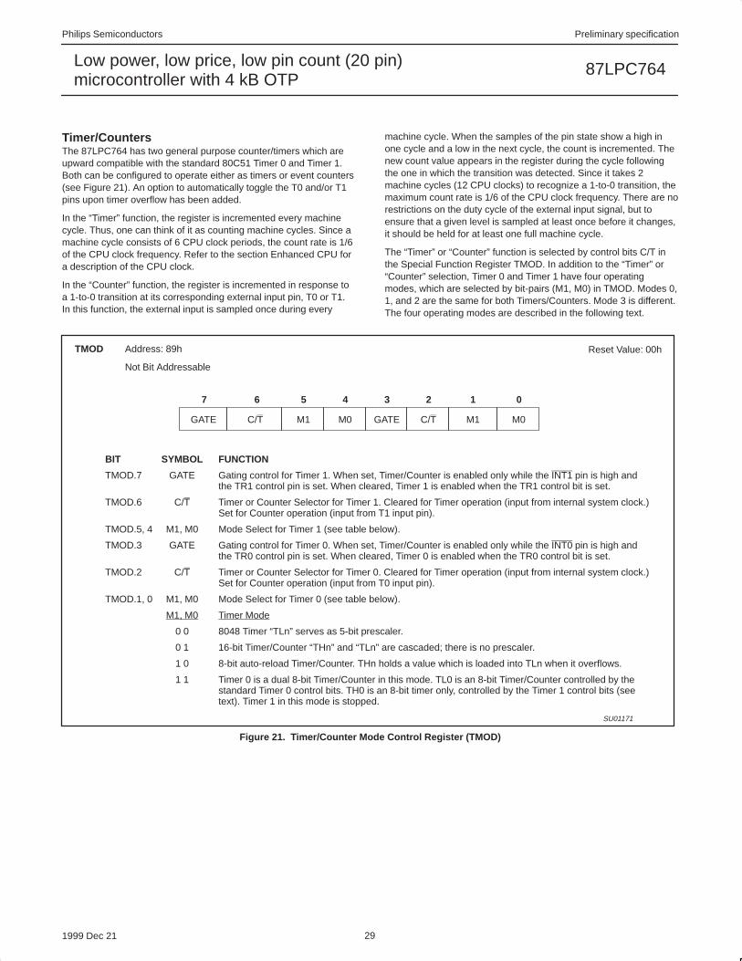
Philips Semiconductors Preliminary specification
87LPC764Low power, low price, low pin count (20 pin)microcontroller with 4 kB OTP
1999 Dec 21 29
Timer/CountersThe 87LPC764 has two general purpose counter/timers which areupward compatible with the standard 80C51 Timer 0 and Timer 1.Both can be configured to operate either as timers or event counters(see Figure 21). An option to automatically toggle the T0 and/or T1pins upon timer overflow has been added.
In the “Timer” function, the register is incremented every machinecycle. Thus, one can think of it as counting machine cycles. Since amachine cycle consists of 6 CPU clock periods, the count rate is 1/6of the CPU clock frequency. Refer to the section Enhanced CPU fora description of the CPU clock.
In the “Counter” function, the register is incremented in response toa 1-to-0 transition at its corresponding external input pin, T0 or T1.In this function, the external input is sampled once during every
machine cycle. When the samples of the pin state show a high inone cycle and a low in the next cycle, the count is incremented. Thenew count value appears in the register during the cycle followingthe one in which the transition was detected. Since it takes 2machine cycles (12 CPU clocks) to recognize a 1-to-0 transition, themaximum count rate is 1/6 of the CPU clock frequency. There are norestrictions on the duty cycle of the external input signal, but toensure that a given level is sampled at least once before it changes,it should be held for at least one full machine cycle.
The “Timer” or “Counter” function is selected by control bits C/T inthe Special Function Register TMOD. In addition to the “Timer” or“Counter” selection, Timer 0 and Timer 1 have four operatingmodes, which are selected by bit-pairs (M1, M0) in TMOD. Modes 0,1, and 2 are the same for both Timers/Counters. Mode 3 is different.The four operating modes are described in the following text.
BIT SYMBOL FUNCTION
TMOD.7 GATE Gating control for Timer 1. When set, Timer/Counter is enabled only while the INT1 pin is high andthe TR1 control pin is set. When cleared, Timer 1 is enabled when the TR1 control bit is set.
TMOD.6 C/T Timer or Counter Selector for Timer 1. Cleared for Timer operation (input from internal system clock.)Set for Counter operation (input from T1 input pin).
TMOD.5, 4 M1, M0 Mode Select for Timer 1 (see table below).
TMOD.3 GATE Gating control for Timer 0. When set, Timer/Counter is enabled only while the INT0 pin is high andthe TR0 control pin is set. When cleared, Timer 0 is enabled when the TR0 control bit is set.
TMOD.2 C/T Timer or Counter Selector for Timer 0. Cleared for Timer operation (input from internal system clock.)Set for Counter operation (input from T0 input pin).
TMOD.1, 0 M1, M0 Mode Select for Timer 0 (see table below).
M1, M0 Timer Mode
0 0 8048 Timer “TLn” serves as 5-bit prescaler.
0 1 16-bit Timer/Counter “THn” and “TLn” are cascaded; there is no prescaler.
1 0 8-bit auto-reload Timer/Counter. THn holds a value which is loaded into TLn when it overflows.
1 1 Timer 0 is a dual 8-bit Timer/Counter in this mode. TL0 is an 8-bit Timer/Counter controlled by thestandard Timer 0 control bits. TH0 is an 8-bit timer only, controlled by the Timer 1 control bits (seetext). Timer 1 in this mode is stopped.
M0
SU01171
M1C/TGATEM0M1C/TGATE
01234567
TMOD Reset Value: 00h
Not Bit Addressable
Address: 89h
Figure 21. Timer/Counter Mode Control Register (TMOD)

Philips Semiconductors Preliminary specification
87LPC764Low power, low price, low pin count (20 pin)microcontroller with 4 kB OTP
1999 Dec 21 30
Mode 0Putting either Timer into Mode 0 makes it look like an 8048 Timer,which is an 8-bit Counter with a divide-by-32 prescaler. Figure 23shows Mode 0 operation.
In this mode, the Timer register is configured as a 13-bit register. Asthe count rolls over from all 1s to all 0s, it sets the Timer interruptflag TFn. The count input is enabled to the Timer when TRn = 1 andeither GATE = 0 or INTn = 1. (Setting GATE = 1 allows the Timer tobe controlled by external input INTn, to facilitate pulse width
measurements). TRn is a control bit in the Special Function RegisterTCON (Figure 22). The GATE bit is in the TMOD register.
The 13-bit register consists of all 8 bits of THn and the lower 5 bitsof TLn. The upper 3 bits of TLn are indeterminate and should beignored. Setting the run flag (TRn) does not clear the registers.
Mode 0 operation is the same for Timer 0 and Timer 1. SeeFigure 23. There are two different GATE bits, one for Timer 1(TMOD.7) and one for Timer 0 (TMOD.3).
BIT SYMBOL FUNCTION
TCON.7 TF1 Timer 1 overflow flag. Set by hardware on Timer/Counter overflow. Cleared by hardware when theinterrupt is processed, or by software.
TCON.6 TR1 Timer 1 Run control bit. Set/cleared by software to turn Timer/Counter 1 on/off.
TCON.5 TF0 Timer 0 overflow flag. Set by hardware on Timer/Counter overflow. Cleared by hardware when theprocessor vectors to the interrupt routine, or by software.
TCON.4 TR0 Timer 0 Run control bit. Set/cleared by software to turn Timer/Counter 0 on/off.
TCON.3 IE1 Interrupt 1 Edge flag. Set by hardware when external interrupt 1 edge is detected. Cleared byhardware when the interrupt is processed, or by software.
TCON.2 IT1 Interrupt 1 Type control bit. Set/cleared by software to specify falling edge/low level triggeredexternal interrupts.
TCON.1 IE0 Interrupt 0 Edge flag. Set by hardware when external interrupt 0 edge is detected. Cleared byhardware when the interrupt is processed, or by software.
TCON.0 IT0 Interrupt 0 Type control bit. Set/cleared by software to specify falling edge/low level triggeredexternal interrupts.
IT0
SU01172
IE0IT1IE1TR0TF0TR1TF1
01234567
TCON Reset Value: 00h
Bit Addressable
Address: 88h
Figure 22. Timer/Counter Control Register (TCON)
SU01173
TLN(5-BITS)
THN(8-BITS)
OSC/6 OROSC/12
OVERFLOW
Tn PIN
TnOE
TOGGLE
CONTROLC/T = 1
C/T = 0
Tn PIN
TRn
GATE
INTn PIN
INTERRUPTTFn
Figure 23. Timer/Counter 0 or 1 in Mode 0 (13-Bit Counter)

Philips Semiconductors Preliminary specification
87LPC764Low power, low price, low pin count (20 pin)microcontroller with 4 kB OTP
1999 Dec 21 31
Mode 1Mode 1 is the same as Mode 0, except that all 16 bits of the timerregister (THn and TLn) are used. See Figure 24
Mode 2Mode 2 configures the Timer register as an 8-bit Counter (TL1) withautomatic reload, as shown in Figure 25. Overflow from TLn not onlysets TFn, but also reloads TLn with the contents of THn, which mustbe preset by software. The reload leaves THn unchanged. Mode 2operation is the same for Timer 0 and Timer 1.
Mode 3When Timer 1 is in Mode 3 it is stopped. The effect is the same assetting TR1 = 0.
Timer 0 in Mode 3 establishes TL0 and TH0 as two separate 8-bitcounters. The logic for Mode 3 on Timer 0 is shown in Figure 26.TL0 uses the Timer 0 control bits: C/T, GATE, TR0, INT0, and TF0.TH0 is locked into a timer function (counting machine cycles) andtakes over the use of TR1 and TF1 from Timer 1. Thus, TH0 nowcontrols the “Timer 1” interrupt.
Mode 3 is provided for applications that require an extra 8-bit timer.With Timer 0 in Mode 3, an 87LPC764 can look like it has threeTimer/Counters. When Timer 0 is in Mode 3, Timer 1 can be turnedon and off by switching it into and out of its own Mode 3. It can stillbe used by the serial port as a baud rate generator, or in anyapplication not requiring an interrupt.
SU01174
TLN(8-BITS)
THN(8-BITS)
OSC/6 OROSC/12
OVERFLOW
Tn PIN
TnOE
TOGGLE
CONTROLC/T = 1
C/T = 0
Tn PIN
TRn
GATE
INTn PIN
INTERRUPTTFn
Figure 24. Timer/Counter 0 or 1 in Mode 1 (16-Bit Counter)
SU01175
TLN(8-BITS)
THN(8-BITS)
OSC/6 OROSC/12 OVERFLOW
Tn PIN
Tine
TOGGLE
CONTROLC/T = 1
C/T = 0
Tn PIN
TRn
GATE
INTn PIN
INTERRUPTTFn
RELOAD
Figure 25. Timer/Counter 0 or 1 in Mode 2 (8-Bit Auto-Reload)

Philips Semiconductors Preliminary specification
87LPC764Low power, low price, low pin count (20 pin)microcontroller with 4 kB OTP
1999 Dec 21 32
SU01176
TL0(8-BITS)
OSC/6 OROSC/12 OVERFLOW
T0 PIN
T0OE
TOGGLE
CONTROLC/T = 1
C/T = 0
T0 PIN
TR0
GATE
INT0 PIN
INTERRUPTTF0
TH0(8-BITS)
OVERFLOW
T1 PIN
T1OE
TOGGLE
CONTROL
INTERRUPTTF1
TR1
OSC/6 OROSC/12
Figure 26. Timer/Counter 0 Mode 3 (Two 8-Bit Counters)
Timer Overflow Toggle OutputTimers 0 and 1 can be configured to automatically toggle a portoutput whenever a timer overflow occurs. The same device pins thatare used for the T0 and T1 count inputs are also used for the timertoggle outputs. This function is enabled by control bits ENT0 andENT1 in the P2M1 register, and apply to Timer 0 and Timer 1respectively. The port outputs will be a logic 1 prior to the first timeroverflow when this mode is turned on.
UARTThe 87LPC764 includes an enhanced 80C51 UART. The baud ratesource for the UART is timer 1 for modes 1 and 3, while the rate isfixed in modes 0 and 2. Because CPU clocking is different on the87LPC764 than on the standard 80C51, baud rate calculation issomewhat different. Enhancements over the standard 80C51 UARTinclude Framing Error detection and automatic address recognition.
The serial port is full duplex, meaning it can transmit and receivesimultaneously. It is also receive-buffered, meaning it cancommence reception of a second byte before a previously receivedbyte has been read from the SBUF register. However, if the first bytestill hasn’t been read by the time reception of the second byte iscomplete, the first byte will be lost. The serial port receive andtransmit registers are both accessed through Special FunctionRegister SBUF. Writing to SBUF loads the transmit register, andreading SBUF accesses a physically separate receive register.
The serial port can be operated in 4 modes:
Mode 0Serial data enters and exits through RxD. TxD outputs the shiftclock. 8 bits are transmitted or received, LSB first. The baud rate isfixed at 1/6 of the CPU clock frequency.
Mode 110 bits are transmitted (through TxD) or received (through RxD): astart bit (logical 0), 8 data bits (LSB first), and a stop bit (logical 1).When data is received, the stop bit is stored in RB8 in SpecialFunction Register SCON. The baud rate is variable and isdetermined by the Timer 1 overflow rate.
Mode 211 bits are transmitted (through TxD) or received (through RxD):start bit (logical 0), 8 data bits (LSB first), a programmable 9th databit, and a stop bit (logical 1). When data is transmitted, the 9th databit (TB8 in SCON) can be assigned the value of 0 or 1. Or, forexample, the parity bit (P, in the PSW) could be moved into TB8.When data is received, the 9th data bit goes into RB8 in SpecialFunction Register SCON, while the stop bit is ignored. The baudrate is programmable to either 1/16 or 1/32 of the CPU clockfrequency, as determined by the SMOD1 bit in PCON.
Mode 311 bits are transmitted (through TxD) or received (through RxD): astart bit (logical 0), 8 data bits (LSB first), a programmable 9th databit, and a stop bit (logical 1). In fact, Mode 3 is the same as Mode 2in all respects except baud rate. The baud rate in Mode 3 is variableand is determined by the Timer 1 overflow rate.
In all four modes, transmission is initiated by any instruction thatuses SBUF as a destination register. Reception is initiated in Mode 0by the condition RI = 0 and REN = 1. Reception is initiated in theother modes by the incoming start bit if REN = 1.

Philips Semiconductors Preliminary specification
87LPC764Low power, low price, low pin count (20 pin)microcontroller with 4 kB OTP
1999 Dec 21 33
Serial Port Control Register (SCON)The serial port control and status register is the Special FunctionRegister SCON, shown in Figure 27. This register contains not onlythe mode selection bits, but also the 9th data bit for transmit andreceive (TB8 and RB8), and the serial port interrupt bits (TI and RI).
The Framing Error bit (FE) allows detection of missing stop bits inthe received data stream. The FE bit shares the bit position SCON.7
with the SM0 bit. Which bit appears in SCON at any particular timeis determined by the SMOD0 bit in the PCON register. If SMOD0 =0, SCON.7 is the SM0 bit. If SMOD0 = 1, SCON.7 is the FE bit.Once set, the FE bit remains set until it is cleared by software. Thisallows detection of framing errors for a group of characters withoutthe need for monitoring it for every character individually.
BIT SYMBOL FUNCTION
SCON.7 FE Framing Error. This bit is set by the UART receiver when an invalid stop bit is detected. Must becleared by software. The SMOD0 bit in the PCON register must be 1 for this bit to be accessible.See SM0 bit below.
SCON.7 SM0 With SM1, defines the serial port mode. The SMOD0 bit in the PCON register must be 0 for this bitto be accessible. See FE bit above.
SCON. 6 SM1 With SM0, defines the serial port mode (see table below).
SM0, SM1 UART Mode Baud Rate
0 0 0: shift register CPU clock/6
0 1 1: 8-bit UART Variable (see text)
1 0 2: 9-bit UART CPU clock/32 or CPU clock/16
1 1 3: 9-bit UART Variable (see text)
SCON.5 SM2 Enables the multiprocessor communication feature in Modes 2 and 3. In Mode 2 or 3, if SM2 is setto 1, then Rl will not be activated if the received 9th data bit (RB8) is 0. In Mode 1, if SM2=1 then RIwill not be activated if a valid stop bit was not received. In Mode 0, SM2 should be 0.
SCON.4 REN Enables serial reception. Set by software to enable reception. Clear by software to disable reception.
SCON.3 TB8 The 9th data bit that will be transmitted in Modes 2 and 3. Set or clear by software as desired.
SCON.2 RB8 In Modes 2 and 3, is the 9th data bit that was received. In Mode 1, it SM2=0, RB8 is the stop bit thatwas received. In Mode 0, RB8 is not used.
SCON.1 TI Transmit interrupt flag. Set by hardware at the end of the 8th bit time in Mode 0, or at the beginningof the stop bit in the other modes, in any serial transmission. Must be cleared by software.
SCON.0 RI Receive interrupt flag. Set by hardware at the end of the 8th bit time in Mode 0, or halfway throughthe stop bit time in the other modes, in any serial reception (except see SM2). Must be cleared bysoftware.
RI
SU01157
TIRB8TB8RENSM2SM1SM0/FE
01234567
SCON Reset Value: 00h
Bit Addressable
Address: 98h
Figure 27. Serial Port Control Register (SCON)
Philips Semiconductors Preliminary specification
87LPC764Low power, low price, low pin count (20 pin)microcontroller with 4 kB OTP
1999 Dec 21 34
Baud RatesThe baud rate in Mode 0 is fixed: Mode 0 Baud Rate = CPU clock/6.The baud rate in Mode 2 depends on the value of bit SMOD1 inSpecial Function Register PCON. If SMOD1 = 0 (which is the valueon reset), the baud rate is 1/32 of the CPU clock frequency. IfSMOD1 = 1, the baud rate is 1/16 of the CPU clock frequency.
Mode 2 Baud Rate � 1 � SMOD132
� CPU clock frequency
Using Timer 1 to Generate Baud RatesWhen Timer 1 is used as the baud rate generator, the baud rates inModes 1 and 3 are determined by the Timer 1 overflow rate and thevalue of SMOD1. The Timer 1 interrupt should be disabled in this
application. The Timer itself can be configured for either “timer” or“counter” operation, and in any of its 3 running modes. In the mosttypical applications, it is configured for “timer” operation, in theauto-reload mode (high nibble of TMOD = 0010b). In that case thebaud rate is given by the formula:
Mode 1, 3 Baud Rate �
CPU clock frequency�192 (or 96 if SMOD1 � 1)
256 � (TH1)
Tables 6 and 7 list various commonly used baud rates and how theycan be obtained using Timer 1 as the baud rate generator.
Table 9. Baud Rates, Timer Values, and CPU Clock Frequencies for SMOD1 = 0
Timer Co ntBaud Rate
Timer Count2400 4800 9600 19.2k 38.4k 57.6k
–1 0.4608 0.9216 * 1.8432 * 3.6864 * 7.3728 * 11.0592
–2 0.9216 1.8432 * 3.6864 * 7.3728 * 14.7456
–3 1.3824 2.7648 5.5296 * 11.0592 – –
–4 * 1.8432 * 3.6864 * 7.3728 * 14.7456 – –
–5 2.3040 4.6080 9.2160 * 18.4320 – –
–6 2.7648 5.5296 * 11.0592 – – –
–7 3.2256 6.4512 12.9024 – – –
–8 * 3.6864 * 7.3728 * 14.7456 – – –
–9 4.1472 8.2944 16.5888 – – –
–10 4.6080 9.2160 * 18.4320 – – –

Philips Semiconductors Preliminary specification
87LPC764Low power, low price, low pin count (20 pin)microcontroller with 4 kB OTP
1999 Dec 21 35
Table 10. Baud Rates, Timer Values, and CPU Clock Frequencies for SMOD1 = 1
Timer Co ntBaud Rate
Timer Count2400 4800 9600 19.2k 38.4k 57.6k 115.2k
–1 0.2304 0.4608 0.9216 * 1.8432 * 3.6864 5.5296 * 11.0592
–2 0.4608 0.9216 * 1.8432 * 3.6864 * 7.3728 * 11.0592 –
–3 0.6912 1.3824 2.7648 5.5296 * 11.0592 16.5888 –
–4 0.9216 * 1.8432 * 3.6864 * 7.3728 * 14.7456 – –
–5 1.1520 2.3040 4.6080 9.2160 * 18.4320 – –
–6 1.3824 2.7648 5.5296 * 11.0592 – – –
–7 1.6128 3.2256 6.4512 12.9024 – – –
–8 * 1.8432 * 3.6864 * 7.3728 * 14.7456 – – –
–9 2.0736 4.1472 8.2944 16.5888 – – –
–10 2.3040 4.6080 9.2160 * 18.4320 – – –
–11 2.5344 5.0688 10.1376 – – – –
–12 2.7648 5.5296 * 11.0592 – – – –
–13 2.9952 5.9904 11.9808 – – – –
–14 3.2256 6.4512 12.9024 – – – –
–15 3.4560 6.9120 13.8240 – – – –
–16 * 3.6864 * 7.3728 * 14.7456 – – – –
–17 3.9168 7.8336 15.6672 – – – –
–18 4.1472 8.2944 16.5888 – – – –
–19 4.3776 8.7552 17.5104 – – – –
–20 4.6080 9.2160 * 18.4320 – – – –
–21 4.8384 9.6768 19.3536 – – – –
NOTES TO TABLES 9 AND 10:1. Tables 6 and 7 apply to UART modes 1 and 3 (variable rate modes), and show CPU clock rates in MHz for standard baud rates from 2400 to
115.2k baud.2. Table 6 shows timer settings and CPU clock rates with the SMOD1 bit in the PCON register = 0 (the default after reset), while Table 7
reflects the SMOD1 bit = 1.3. The tables show all potential CPU clock frequencies up to 20 MHz that may be used for baud rates from 9600 baud to 115.2k baud. Other
CPU clock frequencies that would give only lower baud rates are not shown.4. Table entries marked with an asterisk (*) indicate standard crystal and ceramic resonator frequencies that may be obtained from many
sources without special ordering.

Philips Semiconductors Preliminary specification
87LPC764Low power, low price, low pin count (20 pin)microcontroller with 4 kB OTP
1999 Dec 21 36
More About UART Mode 0Serial data enters and exits through RxD. TxD outputs the shiftclock. 8 bits are transmitted/received: 8 data bits (LSB first). Thebaud rate is fixed at 1/6 the CPU clock frequency. Figure 28 showsa simplified functional diagram of the serial port in Mode 0, andassociated timing.
Transmission is initiated by any instruction that uses SBUF as adestination register. The “write to SBUF” signal at S6P2 also loads a1 into the 9th position of the transmit shift register and tells the TXControl block to commence a transmission. The internal timing issuch that one full machine cycle will elapse between “write to SBUF”and activation of SEND.
SEND enables the output of the shift register to the alternate outputfunction line of P1.1 and also enable SHIFT CLOCK to the alternateoutput function line of P1.0. SHIFT CLOCK is low during S3, S4, andS5 of every machine cycle, and high during S6, S1, and S2. AtS6P2 of every machine cycle in which SEND is active, the contentsof the transmit shift are shifted to the right one position.
As data bits shift out to the right, zeros come in from the left. Whenthe MSB of the data byte is at the output position of the shift register,then the 1 that was initially loaded into the 9th position, is just to theleft of the MSB, and all positions to the left of that contain zeros. Thiscondition flags the TX Control block to do one last shift and thendeactivate SEND and set T1. Both of these actions occur at S1P1 ofthe 10th machine cycle after “write to SBUF.” Reception is initiated bythe condition REN = 1 and R1 = 0. At S6P2 of the next machinecycle, the RX Control unit writes the bits 11111110 t o the receive shiftregister, and in the next clock phase activates RECEIVE.
RECEIVE enable SHIFT CLOCK to the alternate output function lineof P1.0. SHIFT CLOCK makes transitions at S3P1 and S6P1 of everymachine cycle. At S6P2 of every machine cycle in which RECEIVE isactive, the contents of the receive shift register are shifted to the leftone position. The value that comes in from the right is the value thatwas sampled at the P1.1 pin at S5P2 of the same machine cycle.
As data bits come in from the right, 1s shift out to the left. When the 0that was initially loaded into the rightmost position arrives at theleftmost position in the shift register, it flags the RX Control block to doone last shift and load SBUF. At S1P1 of the 10th machine cycle afterthe write to SCON that cleared RI, RECEIVE is cleared as RI is set.
More About UART Mode 1Ten bits are transmitted (through TxD), or received (through RxD): astart bit (0), 8 data bits (LSB first), and a stop bit (1). On receive, thestop bit goes into RB8 in SCON. In the 87LPC764 the baud rate isdetermined by the Timer 1 overflow rate. Figure 29 shows asimplified functional diagram of the serial port in Mode 1, andassociated timings for transmit receive.
Transmission is initiated by any instruction that uses SBUF as adestination register. The “write to SBUF” signal also loads a 1 intothe 9th bit position of the transmit shift register and flags the TXControl unit that a transmission is requested. Transmission actuallycommences at S1P1 of the machine cycle following the next rolloverin the divide-by-16 counter. (Thus, the bit times are synchronized tothe divide-by-16 counter, not to the “write to SBUF” signal.)
The transmission begins with activation of SEND which puts thestart bit at TxD. One bit time later, DATA is activated, which enablesthe output bit of the transmit shift register to TxD. The first shift pulseoccurs one bit time after that.
As data bits shift out to the right, zeros are clocked in from the left.When the MSB of the data byte is at the output position of the shiftregister, then the 1 that was initially loaded into the 9th position isjust to the left of the MSB, and all positions to the left of that containzeros. This condition flags the TX Control unit to do one last shiftand then deactivate SEND and set TI. This occurs at the 10thdivide-by-16 rollover after “write to SBUF.”
Reception is initiated by a detected 1-to-0 transition at RxD. For thispurpose RxD is sampled at a rate of 16 times whatever baud ratehas been established. When a transition is detected, thedivide-by-16 counter is immediately reset, and 1FFH is written intothe input shift register. Resetting the divide-by-16 counter aligns itsrollovers with the boundaries of the incoming bit times.
The 16 states of the counter divide each bit time into 16ths. At the7th, 8th, and 9th counter states of each bit time, the bit detectorsamples the value of RxD. The value accepted is the value that wasseen in at least 2 of the 3 samples. This is done for noise rejection.If the value accepted during the first bit time is not 0, the receivecircuits are reset and the unit goes back to looking for another 1-to-0transition. This is to provide rejection of false start bits. If the start bitproves valid, it is shifted into the input shift register, and reception ofthe rest of the frame will proceed.
As data bits come in from the right, 1s shift out to the left. When thestart bit arrives at the leftmost position in the shift register (which inmode 1 is a 9-bit register), it flags the RX Control block to do onelast shift, load SBUF and RB8, and set RI. The signal to load SBUFand RB8, and to set RI, will be generated if, and only if, the followingconditions are met at the time the final shift pulse is generated.: 1.R1 = 0, and 2. Either SM2 = 0, or the received stop bit = 1.
If either of these two conditions is not met, the received frame isirretrievably lost. If both conditions are met, the stop bit goes intoRB8, the 8 data bits go into SBUF, and RI is activated. At this time,whether the above conditions are met or not, the unit goes back tolooking for a 1-to-0 transition in RxD.

Philips Semiconductors Preliminary specification
87LPC764Low power, low price, low pin count (20 pin)microcontroller with 4 kB OTP
1999 Dec 21 37
80C51 INTERNAL BUS
SU01178
80C51 INTERNAL BUS
WRITETOSBUF
SBUF
ZERO DETECTOR
RxDP1.1 ALTOUTPUT
FUNCTION
TX CONTROL
S
TX CLOCK
START
QCL
D
SERIAL PORTINTERRUPT
SHIFTCLOCK
SHIFT
SENDS6
RXDP1.1 ALT
INPUTFUNCTION
LOADSBUF
TI
INPUT SHIFT REGISTER
START
RI RECEIVE
SHIFT
TX CLOCK
RX CONTROLRENRI
SBUF
READSBUF
TRANSMIT
TxDP1.0 ALTOUTPUT
FUNCTION
SEND
RXD (DATA OUT) D0 D1 D5D2 D6D3 D4 D7
TXD (SHIFT CLOCK)
SHIFT
S1 ... S6 S1 ... S6 S1 ... S6 S1 ... S6S1 ... S6S1 ... S6 S1 ... S6 S1 ... S6 S1 ... S6 S1 ... S6S1 ... S6S1 ... S6 S1 ... S6
WRITE TO SBUF
TI
RECEIVERECEIVE
D0 D1 D5D2 D6D3 D4 D7
TxD (SHIFT CLOCK)
SHIFT
WRITE TO SCON (CLEAR RI)
RI
RxD (DATA IN)
1 1 1 1 11 1 0
Figure 28. Serial Port Mode 0

Philips Semiconductors Preliminary specification
87LPC764Low power, low price, low pin count (20 pin)microcontroller with 4 kB OTP
1999 Dec 21 38
SU01179
80C51 INTERNAL BUS
WRITETO SBUF
SBUF
ZERO DETECTOR
TxDP1.0 ALTOUTPUT
FUNCTION
TX CONTROL
S
TX CLOCK
START
QCL
D
SERIAL PORTINTERRUPT
SHIFT
SEND
LOADSBUF
TI
INPUT SHIFT REGISTER
START
RI LOAD SBUF
SHIFT
RXCLOCK
1FFH
RX CONTROL
SBUF
READSBUF
TRANSMIT
RxDP1.1 ALT
INPUTFUNCTION
80C51 INTERNAL BUS
DATA
TB8
÷16
÷16
÷2
TIMER 1OVERFLOW
SMOD1 = 0 SMOD1= 1
1-TO-0TRANSITIONDETECTOR
BITDETECTOR
STARTBIT STOP BIT
TX CLOCK
WRITE TO SBUF
SEND
DATA
SHIFT
TxD
TI
D0 D1 D5D2 D6D3 D4 D7
RECEIVE
RX CLOCK
SHIFT
RI
BIT DETECTOR SAMPLE TIMES
STARTBIT STOP BITRxD D0 D1 D5D2 D6D3 D4 D7÷ 16 RESET
Figure 29. Serial Port Mode 1

Philips Semiconductors Preliminary specification
87LPC764Low power, low price, low pin count (20 pin)microcontroller with 4 kB OTP
1999 Dec 21 39
More About UART Modes 2 and 3Eleven bits are transmitted (through TxD), or received (throughRxD): a start bit (0), 8 data bits (LSB first), a programmable 9th databit, and a stop bit (1). On transmit, the 9th data bit (TB8) can beassigned the value of 0 or 1. On receive, the 9the data bit goes intoRB8 in SCON. The baud rate is programmable to either 1/16 or 1/32of the CPU clock frequency in Mode 2. Mode 3 may have a variablebaud rate generated from Timer 1.
Figures 30 and 31 show a functional diagram of the serial port inModes 2 and 3. The receive portion is exactly the same as in Mode 1.The transmit portion differs from Mode 1 only in the 9th bit of thetransmit shift register.
Transmission is initiated by any instruction that uses SBUF as adestination register. The “write to SBUF” signal also loads TB8 intothe 9th bit position of the transmit shift register and flags the TXControl unit that a transmission is requested. Transmissioncommences at S1P1 of the machine cycle following the next rolloverin the divide-by-16 counter. (Thus, the bit times are synchronized tothe divide-by-16 counter, not to the “write to SBUF” signal.)
The transmission begins with activation of SEND, which puts thestart bit at TxD. One bit time later, DATA is activated, which enablesthe output bit of the transmit shift register to TxD. The first shift pulseoccurs one bit time after that. The first shift clocks a 1 (the stop bit)into the 9th bit position of the shift register. Thereafter, only zerosare clocked in. Thus, as data bits shift out to the right, zeros areclocked in from the left. When TB8 is at the output position of theshift register, then the stop bit is just to the left of TB8, and allpositions to the left of that contain zeros. This condition flags the TXControl unit to do one last shift and then deactivate SEND and setTI. This occurs at the 11th divide-by-16 rollover after “write to SBUF.”
Reception is initiated by a detected 1-to-0 transition at RxD. For thispurpose RxD is sampled at a rate of 16 times whatever baud ratehas been established. When a transition is detected, thedivide-by-16 counter is immediately reset, and 1FFH is written to theinput shift register.
At the 7th, 8th, and 9th counter states of each bit time, the bitdetector samples the value of R–D. The value accepted is the valuethat was seen in at least 2 of the 3 samples. If the value acceptedduring the first bit time is not 0, the receive circuits are reset and theunit goes back to looking for another 1-to-0 transition. If the start bit
proves valid, it is shifted into the input shift register, and reception ofthe rest of the frame will proceed.
As data bits come in from the right, 1s shift out to the left. When thestart bit arrives at the leftmost position in the shift register (which inModes 2 and 3 is a 9-bit register), it flags the RX Control block to doone last shift, load SBUF and RB8, and set RI.
The signal to load SBUF and RB8, and to set RI, will be generatedif, and only if, the following conditions are met at the time the finalshift pulse is generated. 1. RI = 0, and 2. Either SM2 = 0, or thereceived 9th data bit = 1.
If either of these conditions is not met, the received frame isirretrievably lost, and RI is not set. If both conditions are met, thereceived 9th data bit goes into RB8, and the first 8 data bits go intoSBUF. One bit time later, whether the above conditions were metor not, the unit goes back to looking for a 1-to-0 transition at theRxD input.
Multiprocessor CommunicationsUART modes 2 and 3 have a special provision for multiprocessorcommunications. In these modes, 9 data bits are received ortransmitted. When data is received, the 9th bit is stored in RB8. TheUART can be programmed such that when the stop bit is received,the serial port interrupt will be activated only if RB8 = 1. This featureis enabled by setting bit SM2 in SCON. One way to use this featurein multiprocessor systems is as follows:
When the master processor wants to transmit a block of data to oneof several slaves, it first sends out an address byte which identifiesthe target slave. An address byte differs from a data byte in that the9th bit is 1 in an address byte and 0 in a data byte. With SM2 = 1, noslave will be interrupted by a data byte. An address byte, however,will interrupt all slaves, so that each slave can examine the receivedbyte and see if it is being addressed. The addressed slave will clearits SM2 bit and prepare to receive the data bytes that follow. Theslaves that weren’t being addressed leave their SM2 bits set and goon about their business, ignoring the subsequent data bytes.
SM2 has no effect in Mode 0, and in Mode 1 can be used to checkthe validity of the stop bit, although this is better done with theFraming Error flag. In a Mode 1 reception, if SM2 = 1, the receiveinterrupt will not be activated unless a valid stop bit is received.

Philips Semiconductors Preliminary specification
87LPC764Low power, low price, low pin count (20 pin)microcontroller with 4 kB OTP
1999 Dec 21 40
STARTBIT
SU01180
80C51 INTERNAL BUS
WRITE TO SBUF
SBUF
ZERO DETECTOR
TxDP1.0 ALT OUTPUTFUNCTION
TX CONTROL
S
TX CLOCK
START
QCL
D
SERIAL PORT INTERRUPT
SHIFT
SEND
LOADSBUF
TI
INPUT SHIFT REGISTER
START
RI LOAD SBUF
SHIFT
RXCLOCK
1FFH
RX CONTROL
SBUF
READSBUF
RxDP1.1 ALT
INPUTFUNCTION
80C51 INTERNAL BUS
DATA
TB8
÷16
÷16
÷2
PHASE 2 CLOCK(1/2 fOSC)
1-TO-0TRANSITIONDETECTOR
BIT DETECTOR
STOP BIT GEN.
SMOD1 = 0 SMOD1= 1
TRANSMIT
STARTBIT STOP BIT
TX CLOCK
WRITE TO SBUF
SEND
DATA
SHIFT
TxD
TI
D0 D1 D5D2 D6D3 D4 D7
RECEIVE
RX CLOCK
SHIFT
RI
BIT DETECTOR SAMPLE TIMES
STOP BITRxD D0 D1 D5D2 D6D3 D4 D7÷ 16 RESET
TB8
STOP BIT GEN.
RB8
Figure 30. Serial Port Mode 2

Philips Semiconductors Preliminary specification
87LPC764Low power, low price, low pin count (20 pin)microcontroller with 4 kB OTP
1999 Dec 21 41
BITDETECTOR
SU01181
TRANSMIT
STARTBIT STOP BIT
TX CLOCK
WRITE TO SBUF
SEND
DATA
SHIFT
TxD
TI
D0 D1 D5D2 D6D3 D4 D7
RECEIVE
RX CLOCK
SHIFT
RI
BIT DETECTOR SAMPLE TIMES
STARTBIT STOP BITRxD D0 D1 D5D2 D6D3 D4 D7÷ 16 RESET
TB8
STOP BIT GEN.
RB8
80C51 INTERNAL BUS
WRITE TO SBUF
SBUF
ZERO DETECTOR
TxDP1.0 ALTOUTPUTFUNCTION
TX CONTROL
S
TX CLOCK
START
QCL
D
SERIAL PORT INTERRUPT
SHIFT
SEND
LOADSBUF
TI
INPUT SHIFT REGISTER
START
RI LOAD SBUF
SHIFT
RXCLOCK
1FFH
RX CONTROL
SBUF
READSBUF
RxDP1.1 ALT
INPUTFUNCTION
80C51 INTERNAL BUS
DATA
TB8
÷16
÷16
÷2
TIMER 1OVERFLOW
SMOD1 = 0 SMOD1= 1
1-TO-0TRANSITIONDETECTOR
Figure 31. Serial Port Mode 3

Philips Semiconductors Preliminary specification
87LPC764Low power, low price, low pin count (20 pin)microcontroller with 4 kB OTP
1999 Dec 21 42
Automatic Address RecognitionAutomatic Address Recognition is a feature which allows the UARTto recognize certain addresses in the serial bit stream by usinghardware to make the comparisons. This feature saves a great dealof software overhead by eliminating the need for the software toexamine every serial address which passes by the serial port. Thisfeature is enabled by setting the SM2 bit in SCON. In the 9 bit UARTmodes, mode 2 and mode 3, the Receive Interrupt flag (RI) will beautomatically set when the received byte contains either the “Given”address or the “Broadcast” address. The 9 bit mode requires thatthe 9th information bit is a 1 to indicate that the received informationis an address and not data.
Using the Automatic Address Recognition feature allows a master toselectively communicate with one or more slaves by invoking theGiven slave address or addresses. All of the slaves may becontacted by using the Broadcast address. Two special FunctionRegisters are used to define the slave’s address, SADDR, and theaddress mask, SADEN. SADEN is used to define which bits in theSADDR are to be used and which bits are “don’t care”. The SADENmask can be logically ANDed with the SADDR to create the “Given”address which the master will use for addressing each of the slaves.Use of the Given address allows multiple slaves to be recognizedwhile excluding others. The following examples will help to show theversatility of this scheme:
Slave 0 SADDR = 1100 0000SADEN = 1111 1101Given = 1100 00X0
Slave 1 SADDR = 1100 0000SADEN = 1111 1110Given = 1100 000X
In the above example SADDR is the same and the SADEN data isused to differentiate between the two slaves. Slave 0 requires a 0 inbit 0 and it ignores bit 1. Slave 1 requires a 0 in bit 1 and bit 0 isignored. A unique address for Slave 0 would be 1100 0010 sinceslave 1 requires a 0 in bit 1. A unique address for slave 1 would be1100 0001 since a 1 in bit 0 will exclude slave 0. Both slaves can beselected at the same time by an address which has bit 0 = 0 (forslave 0) and bit 1 = 0 (for slave 1). Thus, both could be addressedwith 1100 0000.
In a more complex system the following could be used to selectslaves 1 and 2 while excluding slave 0:
Slave 0 SADDR = 1100 0000SADEN = 1111 1001Given = 1100 0XX0
Slave 1 SADDR = 1110 0000SADEN = 1111 1010Given = 1110 0X0X
Slave 2 SADDR = 1110 0000SADEN = 1111 1100Given = 1110 00XX
In the above example the differentiation among the 3 slaves is in thelower 3 address bits. Slave 0 requires that bit 0 = 0 and it can beuniquely addressed by 1110 0110. Slave 1 requires that bit 1 = 0 andit can be uniquely addressed by 1110 and 0101. Slave 2 requiresthat bit 2 = 0 and its unique address is 1110 0011. To select Slaves 0and 1 and exclude Slave 2 use address 1110 0100, since it isnecessary to make bit 2 = 1 to exclude slave 2. The BroadcastAddress for each slave is created by taking the logical OR of SADDRand SADEN. Zeros in this result are treated as don’t-cares. In mostcases, interpreting the don’t-cares as ones, the broadcast address
will be FF hexadecimal. Upon reset SADDR and SADEN are loadedwith 0s. This produces a given address of all “don’t cares” as well asa Broadcast address of all “don’t cares”. This effectively disables theAutomatic Addressing mode and allows the microcontroller to usestandard UART drivers which do not make use of this feature.
Watchdog TimerWhen enabled via the WDTE configuration bit, the watchdog timer isoperated from an independent, fully on-chip oscillator in order toprovide the greatest possible dependability. When the watchdogfeature is enabled, the timer must be fed regularly by software inorder to prevent it from resetting the CPU, and it cannot be turned off.When disabled as a watchdog timer (via the WDTE bit in the UCFG1configuration register), it may be used as an interval timer and maygenerate an interrupt. The watchdog timer is shown in Figure 32.
The watchdog timeout time is selectable from one of eight values,nominal times range from 16 milliseconds to 2.1 seconds. Thefrequency tolerance of the independent watchdog RC oscillator is±37%. The timeout selections and other control bits are shown inFigure 33. When the watchdog function is enabled, the WDCONregister may be written once during chip initialization in order to setthe watchdog timeout time. The recommended method of initializingthe WDCON register is to first feed the watchdog, then write toWDCON to configure the WDS2–0 bits. Using this method, thewatchdog initialization may be done any time within 10 millisecondsafter startup without a watchdog overflow occurring before theinitialization can be completed.
Since the watchdog timer oscillator is fully on-chip and independentof any external oscillator circuit used by the CPU, it intrinsicallyserves as an oscillator fail detection function. If the watchdog featureis enabled and the CPU oscillator fails for any reason, the watchdogtimer will time out and reset the CPU.
When the watchdog function is enabled, the timer is deactivatedtemporarily when a chip reset occurs from another source, such asa power on reset, brownout reset, or external reset.
Watchdog Feed SequenceIf the watchdog timer is running, it must be fed before it times out inorder to prevent a chip reset from occurring. The watchdog feedsequence consists of first writing the value 1Eh, then the value E1hto the WDRST register. An example of a watchdog feed sequence isshown below.
WDFeed:mov WDRST,#1eh ; First part of watchdog feed sequence.mov WDRST,#0e1h ; Second part of watchdog feed sequence.
The two writes to WDRST do not have to occur in consecutiveinstructions. An incorrect watchdog feed sequence does not causeany immediate response from the watchdog timer, which will stilltime out at the originally scheduled time if a correct feed sequencedoes not occur prior to that time.
After a chip reset, the user program has a limited time in which toeither feed the watchdog timer or change the timeout period. Whena low CPU clock frequency is used in the application, the number ofinstructions that can be executed before the watchdog overflowsmay be quite small.
Watchdog ResetIf a watchdog reset occurs, the internal reset is active forapproximately one microsecond. If the CPU clock was still running,code execution will begin immediately after that. If the processorwas in Power Down mode, the watchdog reset will start the oscillatorand code execution will resume after the oscillator is stable.

Philips Semiconductors Preliminary specification
87LPC764Low power, low price, low pin count (20 pin)microcontroller with 4 kB OTP
1999 Dec 21 43
SU01182
WATCHDOGINTERRUPT
S
Q
20-BIT COUNTER
STATE CLOCK
WDTE (UCFG1.7)
BOD (xxx.x)
POR (xxx.x)
WATCHDOGRESET
CLEAR
8 MSBs
8 TO 1 MUX
WATCHDOGFEED DETECT
WDOVF(WDCON.5)
WDS2–0(WDCON.2–0)
WDTE + WDRUN
WDCLK * WDTE
500 kHzR/C OSCILLATOR
ENABLE
CLOCK OUT
R
Figure 32. Block Diagram of the Watchdog Timer
BIT SYMBOL FUNCTION
WDCON.7, 6 — Reserved for future use. Should not be set to 1 by user programs.
WDCON.5 WDOVF Watchdog timer overflow flag. Set when a watchdog reset or timer overflow occurs. Cleared whenthe watchdog is fed.
WDCON.4 WDRUN Watchdog run control. The watchdog timer is started when WDRUN = 1 and stopped whenWDRUN = 0. This bit is forced to 1 (watchdog running) if the WDTE configuration bit = 1.
WDCON.3 WDCLK Watchdog clock select. The watchdog timer is clocked by CPU clock/6 when WDCLK = 1 and bythe watchdog RC oscillator when WDCLK = 0. This bit is forced to 0 (using the watchdog RCoscillator) if the WDTE configuration bit = 1.
WDCON.2–0 WDS2–0 Watchdog rate select.
WDS2–0 Timeout Clocks Minimum Time Nominal Time Maximum Time
0 0 0 8,192 10 ms 16 ms 23 ms
0 0 1 16,384 20 ms 32 ms 45 ms
0 1 0 32,768 41 ms 65 ms 90 ms
0 1 1 65,536 82 ms 131 ms 180 ms
1 0 0 131,072 165 ms 262 ms 360 ms
1 0 1 262,144 330 ms 524 ms 719 ms
1 1 0 524,288 660 ms 1.05 sec 1.44 sec
1 1 1 1,048,576 1.3 sec 2.1 sec 2.9 sec
WDS0
SU01183
WDS1WDS2WDCLKWDRUNWDOVF——
01234567
WDCON Reset Value: � 30h for a watchdog reset.
� 10h for other rest sources if the watchdog is enabled via the WDTE configuration bit.
� 00h for other reset sources if the watchdog is disabled via the WDTE configuration bit.
Not Bit Addressable
Address: A7h
Figure 33. Watchdog Timer Control Register (WDCON)

Philips Semiconductors Preliminary specification
87LPC764Low power, low price, low pin count (20 pin)microcontroller with 4 kB OTP
1999 Dec 21 44
Additional FeaturesThe AUXR1 register contains several special purpose control bits thatrelate to several chip features. AUXR1 is described in Figure 34.
Software ResetThe SRST bit in AUXR1 allows software the opportunity to reset theprocessor completely, as if an external reset or watchdog reset hadoccurred. If a value is written to AUXR1 that contains a 1 at bitposition 3, all SFRs will be initialized and execution will resume atprogram address 0000. Care should be taken when writing toAUXR1 to avoid accidental software resets.
Dual Data PointersThe dual Data Pointer (DPTR) adds to the ways in which theprocessor can specify the address used with certain instructions.The DPS bit in the AUXR1 register selects one of the two DataPointers. The DPTR that is not currently selected is not accessibleto software unless the DPS bit is toggled.
Specific instructions affected by the Data Pointer selection are:
• INC DPTR Increments the Data Pointer by 1.
• JMP @A+DPTR Jump indirect relative to DPTR value.
• MOV DPTR, #data16 Load the Data Pointer with a 16-bitconstant.
• MOVC A, @A+DPTR Move code byte relative to DPTR to theaccumulator.
• MOVX A, @DPTR Move data byte the accumulator to datamemory relative to DPTR.
• MOVX @DPTR, A Move data byte from data memoryrelative to DPTR to the accumulator.
Also, any instruction that reads or manipulates the DPH and DPLregisters (the upper and lower bytes of the current DPTR) will beaffected by the setting of DPS. The MOVX instructions have limitedapplication for the 87LPC764 since the part does not have anexternal data bus. However, they may be used to access EPROMconfiguration information (see EPROM Characteristics section).
Bit 2 of AUXR1 is permanently wired as a logic 0. This is so that theDPS bit may be toggled (thereby switching Data Pointers) simply byincrementing the AUXR1 register, without the possibility ofinadvertently altering other bits in the register.
BIT SYMBOL FUNCTION
AUXR1.7 KBF Keyboard Interrupt Flag. Set when any pin of port 0 that is enabled for the Keyboard Interruptfunction goes low. Must be cleared by software.
AUXR1.6 BOD Brown Out Disable. When set, turns off brownout detection and saves power. See PowerMonitoring Functions section for details.
AUXR1.5 BOI Brown Out Interrupt. When set, prevents brownout detection from causing a chip reset and allowsthe brownout detect function to be used as an interrupt. See the Power Monitoring Functionssection for details.
AUXR1.4 LPEP Low Power EPROM control bit. Allows power savings in low voltage systems. Set by software. Canonly be cleared by power-on or brownout reset. See the Power Reduction Modes section fordetails.
AUXR1.3 SRST Software Reset. When set by software, resets the 87LPC764 as if a hardware reset occurred.
AUXR1.2 — This bit contains a hard-wired 0. Allows toggling of the DPS bit by incrementing AUXR1, withoutinterfering with other bits in the register.
AUXR1.1 — Reserved for future use. Should not be set to 1 by user programs.
AUXR1.0 DPS Data Pointer Select. Chooses one of two Data Pointers for use by the program. See text for details.
DPS
SU01184
—0SRSTLPEPBOIBODKBF
01234567
AUXR1 Reset Value: 00h
Not Bit Addressable
Address: A2h
Figure 34. AUXR1 Register
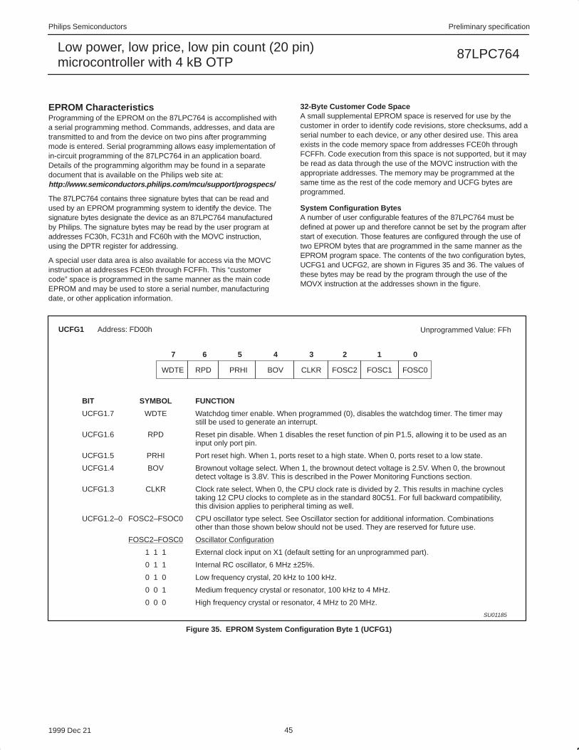
Philips Semiconductors Preliminary specification
87LPC764Low power, low price, low pin count (20 pin)microcontroller with 4 kB OTP
1999 Dec 21 45
EPROM CharacteristicsProgramming of the EPROM on the 87LPC764 is accomplished witha serial programming method. Commands, addresses, and data aretransmitted to and from the device on two pins after programmingmode is entered. Serial programming allows easy implementation ofin-circuit programming of the 87LPC764 in an application board.Details of the programming algorithm may be found in a separatedocument that is available on the Philips web site at:http://www.semiconductors.philips.com/mcu/support/progspecs/
The 87LPC764 contains three signature bytes that can be read andused by an EPROM programming system to identify the device. Thesignature bytes designate the device as an 87LPC764 manufacturedby Philips. The signature bytes may be read by the user program ataddresses FC30h, FC31h and FC60h with the MOVC instruction,using the DPTR register for addressing.
A special user data area is also available for access via the MOVCinstruction at addresses FCE0h through FCFFh. This “customercode” space is programmed in the same manner as the main codeEPROM and may be used to store a serial number, manufacturingdate, or other application information.
32-Byte Customer Code SpaceA small supplemental EPROM space is reserved for use by thecustomer in order to identify code revisions, store checksums, add aserial number to each device, or any other desired use. This areaexists in the code memory space from addresses FCE0h throughFCFFh. Code execution from this space is not supported, but it maybe read as data through the use of the MOVC instruction with theappropriate addresses. The memory may be programmed at thesame time as the rest of the code memory and UCFG bytes areprogrammed.
System Configuration BytesA number of user configurable features of the 87LPC764 must bedefined at power up and therefore cannot be set by the program afterstart of execution. Those features are configured through the use oftwo EPROM bytes that are programmed in the same manner as theEPROM program space. The contents of the two configuration bytes,UCFG1 and UCFG2, are shown in Figures 35 and 36. The values ofthese bytes may be read by the program through the use of theMOVX instruction at the addresses shown in the figure.
BIT SYMBOL FUNCTION
UCFG1.7 WDTE Watchdog timer enable. When programmed (0), disables the watchdog timer. The timer maystill be used to generate an interrupt.
UCFG1.6 RPD Reset pin disable. When 1 disables the reset function of pin P1.5, allowing it to be used as aninput only port pin.
UCFG1.5 PRHI Port reset high. When 1, ports reset to a high state. When 0, ports reset to a low state.
UCFG1.4 BOV Brownout voltage select. When 1, the brownout detect voltage is 2.5V. When 0, the brownoutdetect voltage is 3.8V. This is described in the Power Monitoring Functions section.
UCFG1.3 CLKR Clock rate select. When 0, the CPU clock rate is divided by 2. This results in machine cyclestaking 12 CPU clocks to complete as in the standard 80C51. For full backward compatibility,this division applies to peripheral timing as well.
UCFG1.2–0 FOSC2–FSOC0 CPU oscillator type select. See Oscillator section for additional information. Combinationsother than those shown below should not be used. They are reserved for future use.
FOSC2–FOSC0 Oscillator Configuration
1 1 1 External clock input on X1 (default setting for an unprogrammed part).
0 1 1 Internal RC oscillator, 6 MHz ±25%.
0 1 0 Low frequency crystal, 20 kHz to 100 kHz.
0 0 1 Medium frequency crystal or resonator, 100 kHz to 4 MHz.
0 0 0 High frequency crystal or resonator, 4 MHz to 20 MHz.
FOSC0
SU01185
FOSC1FOSC2CLKRBOVPRHIRPDWDTE
01234567
UCFG1 Unprogrammed Value: FFhAddress: FD00h
Figure 35. EPROM System Configuration Byte 1 (UCFG1)

Philips Semiconductors Preliminary specification
87LPC764Low power, low price, low pin count (20 pin)microcontroller with 4 kB OTP
1999 Dec 21 46
BIT SYMBOL FUNCTION
UCFG2.7, 6 SB2, SB1 EPROM security bits. See table entitled, “EPROM Security Bits” for details.
UCFG2.5–0 — Reserved for future use.
—
SU01186
—————SB1SB2
01234567
UCFG2 Unprogrammed Value: FFhAddress: FD01h
Figure 36. EPROM System Configuration Byte 2 (UCFG2)
Security BitsWhen neither of the security bits are programmed, the code in the EPROM can be verified. When only security bit 1 is programmed, all furtherprogramming of the EPROM is disabled. At that point, only security bit 2 may still be programmed. When both security bits are programmed,EPROM verify is also disabled.
Table 11. EPROM Security BitsSB2 SB1 Protection Description
1 1 Both security bits unprogrammed. No program security features enabled. EPROM is programmable and verifiable.
1 0 Only security bit 1 programmed. Further EPROM programming is disabled. Security bit 2 may still be programmed.
0 1 Only security bit 2 programmed. This combination is not supported.
0 0 Both security bits programmed. All EPROM verification and programming are disabled.
ABSOLUTE MAXIMUM RATINGSPARAMETER RATING UNIT
Operating temperature under bias –55 to +125 °C
Storage temperature range –65 to +150 °C
Voltage on RST/VPP pin to VSS 0 to +11.0 V
Voltage on any other pin to VSS –0.5 to VDD+0.5V V
Maximum IOL per I/O pin 20 mA
Power dissipation (based on package heat transfer, not device power consumption) 1.5 W
NOTES:1. Stresses above those listed under Absolute Maximum Ratings may cause permanent damage to the device. This is a stress rating only and
functional operation of the device at these or any conditions other than those described in the AC and DC Electrical Characteristics sectionof this specification are not implied.
2. This product includes circuitry specifically designed for the protection of its internal devices from the damaging effects of excessive staticcharge. Nonetheless, it is suggested that conventional precautions be taken to avoid applying greater than the rated maximum.
3. Parameters are valid over operating temperature range unless otherwise specified. All voltages are with respect to VSS unless otherwise noted.

Philips Semiconductors Preliminary specification
87LPC764Low power, low price, low pin count (20 pin)microcontroller with 4 kB OTP
1999 Dec 21 47
DC ELECTRICAL CHARACTERISTICSVDD = 2.7 V to 6.0 V unless otherwise specified; Tamb = 0°C to +70°C or –40°C to +85°C, unless otherwise specified.
SYMBOL PARAMETER TEST CONDITIONSLIMITS
UNITSYMBOL PARAMETER TEST CONDITIONSMIN TYP1 MAX
UNIT
I Power supply current operating5.0 V, 20 MHz11 15 20 mA
IDD Power supply current, operating3.0 V, 10 MHz11 4 7 mA
I Power supply current Idle mode5.0 V, 20 MHz11 6 10 mA
IID Power supply current, Idle mode3.0 V, 10 MHz11 2 4 mA
I Power supply current Power Down mode5.0 V11 1 10 m A
IPD Power supply current, Power Down mode3.0 V11 1 5 m A
VRAM RAM keep-alive voltage 1.5 V
V Input low voltage (TTL input)4.0 V < VDD < 6.0 V –0.5 0.2 VDD–0.1 V
VIL Input low voltage (TTL input)2.7 V < VDD < 4.0 V –0.5 0.7 V
VIL1 Negative going threshold (Schmitt input) –0.5 VDD 0.4 VDD 0.3 VDD V
VIH Input high voltage (TTL input) 0.2 VDD+0.9 VDD+0.5 V
VIH1 Positive going threshold (Schmitt input) 0.7 VDD 0.6 VDD VDD+0.5 V
HYS Hysteresis voltage 0.2 VDD V
VOL Output low voltage all ports5, 9 IOL = 3.2 mA, VDD = 2.7 V 0.4 V
VOL1 Output low voltage all ports5, 9 IOL = 20 mA, VDD = 2.7 V 1.0 V
VO Output high voltage all ports3IOH = –20 m A, VDD = 2.7 V VDD–0.7 V
VOH Output high voltage, all ports3IOH = –30 m A, VDD = 4.5 V VDD–0.7 V
VOH1 Output high voltage, all ports4 IOH = –1.0 mA, VDD = 2.7 V VDD–0.7 V
CIO Input/Output pin capacitance10 15 pF
IIL Logical 0 input current, all ports8 VIN = 0.4 V –50 m A
ILI Input leakage current, all ports7 VIN = VIL or VIH ±2 m A
I Logical 1 to 0 transition current all ports3, 6VIN = 1.5 V at VDD = 3.0 V –30 –250 m A
ITL Logical 1 to 0 transition current, all ports3, 6VIN = 2.0 V at VDD = 5.5 V –150 –650 m A
RRST Internal reset pull-up resistor 40 225 k WVBO2.5 Brownout trip voltage with BOV = 112 Tamb = 0°C to +70°C 2.45 2.5 2.65 V
VBO3.8 Brownout trip voltage with BOV = 0 3.45 3.8 3.90 V
VREF Bandgap reference voltage 1.11 1.26 1.41 V
tC (VREF) Bandgap temperature coefficient tbd ppm/°CSS Bandgap supply sensitivity tbd %/V
NOTES:1. Typical ratings are not guaranteed. The values listed are at room temperature, 5 V.2. See other Figures for details.
Active mode: ICC(MAX) = tbdIdle mode: ICC(MAX) = tbd
3. Ports in quasi-bidirectional mode with weak pull-up (applies to all port pins with pull-ups). Does not apply to open drain pins.4. Ports in PUSH-PULL mode. Does not apply to open drain pins.5. In all output modes except high impedance mode.6. Port pins source a transition current when used in quasi-bidirectional mode and externally driven from 1 to 0. This current is highest when
VIN is approximately 2 V.7. Measured with port in high impedance mode. Parameter is guaranteed but not tested at cold temperature.8. Measured with port in quasi-bidirectional mode.9. Under steady state (non-transient) conditions, IOL must be externally limited as follows:
Maximum IOL per port pin: 20 mAMaximum total IOL for all outputs: 80 mAMaximum total IOH for all outputs: 5 mA
If IOL exceeds the test condition, VOL may exceed the related specification. Pins are not guaranteed to sink current greater than the listedtest conditions.
10. Pin capacitance is characterized but not tested.11. The IDD, IID, and IPD specifications are measured using an external clock with the following functions disabled: comparators, brownout
detect, and watchdog timer. For VDD = 3 V, LPEP = 1. Refer to the appropriate figures on the following pages for additional current drawn byeach of these functions and detailed graphs for other frequency and voltage combinations.
12. Devices initially operating at VDD = 2.7V or above and at fOSC = 10 MHz or less are guaranteed to continue to execute instructions correctlyat the brownout trip point. Initial power-on operation below VDD = 2.7 V is not guaranteed.

Philips Semiconductors Preliminary specification
87LPC764Low power, low price, low pin count (20 pin)microcontroller with 4 kB OTP
1999 Dec 21 48
COMPARATOR ELECTRICAL CHARACTERISTICSVDD = 3.0 V to 6.0 V unless otherwise specified; Tamb = 0°C to +70°C or –40°C to +85°C, unless otherwise specified
SYMBOL PARAMETER TEST CONDITIONSLIMITS
UNITSYMBOL PARAMETER TEST CONDITIONSMIN TYP MAX
UNIT
VIO Offset voltage comparator inputs1 ±10 mV
VCR Common mode range comparator inputs 0 VDD–0.3 V
CMRR Common mode rejection ratio1 –50 dB
Response time 250 500 ns
Comparator enable to output valid 10 m s
IIL Input leakage current, comparator 0 < VIN < VDD ±10 m A
NOTE:1. This parameter is guaranteed by characterization, but not tested in production.
AC ELECTRICAL CHARACTERISTICSTamb = 0°C to +70°C or –40°C to +85°C, VDD = 2.7 V to 6.0 V unless otherwise specified, VSS = 0 V1, 2, 3
SYMBOL FIGURE PARAMETERLIMITS
UNITSYMBOL FIGURE PARAMETERMIN MAX
UNIT
External Clock
fC 38 Oscillator frequency (VDD = 4.5 V to 6.0 V) 0 20 MHz
fC 38 Oscillator frequency (VDD = 2.7 V to 6.0 V) 0 10 MHz
tC 38 Clock period and CPU timing cycle 1/fC ns
tCHCX 38 Clock high-time4 20 ns
tCLCX 38 Clock low time4 20 ns
Shift Register
tXLXL 37 Serial port clock cycle time 6tC ns
tQVXH 37 Output data setup to clock rising edge 5tC – 133 ns
tXHQX 37 Output data hold after clock rising edge 1tC – 80 ns
tXHDV 37 Input data setup to clock rising edge 5tC – 133 ns
tXHDX 37 Input data hold after clock rising edge 0 ns
NOTES:1. Parameters are valid over operating temperature range unless otherwise specified.2. Load capacitance for all outputs = 80 pF.3. Parts are guaranteed to operate down to 0 Hz.4. Applies only to an external clock source, not when a crystal is connected to the X1 and X2 pins.

Philips Semiconductors Preliminary specification
87LPC764Low power, low price, low pin count (20 pin)microcontroller with 4 kB OTP
1999 Dec 21 49
CLEAR RI
tXLXL
CLOCK
tXHQX
tQVXH
OUTPUT DATA
WRITE TO SBUF
INPUT DATA
tXHDV
tXHDXSET TI
SET RI
SU01187
71 2 3 4 5 60
VALID VALID VALID VALID VALID VALID VALID VALID
Figure 37. Shift Register Mode Timing
SU01188
VDD – 0.5
0.45V
0.2VDD + 0.9
0.2 VDD – 0.1
tCHCL tCLCH
tCHCX
tCLCX
tC
Figure 38. External Clock Timing
SU01202
100
10
1
10 100
Idd
(uA
)
Frequency (kHz)
6.0 V5.0 V
4.0 V
3.3 V
2.7 V
Figure 39. Typical Idd versus frequency (low frequencyoscillator, 25 °C)
SU01203
1000
100
10
100 10,000
Idd
(uA
)
Frequency (kHz)1,000
6.0 V5.0 V
2.7 V
6.0 V5.0 V
4.0 V3.3 V2.7 V
Figure 40. Typical Idd versus frequency (medium frequencyoscillator, 25 °C)

Philips Semiconductors Preliminary specification
87LPC764Low power, low price, low pin count (20 pin)microcontroller with 4 kB OTP
1999 Dec 21 50
SU01204
10,000
1,000
100
1 100
Idd
(uA
)
Frequency (MHz)
10
6.0 V5.0 V
4.0 V3.3 V
2.7 V
Figure 41. Typical Idd versus frequency (high frequencyoscillator, 25 °C)
SU01205
100,000
100
10
10 100,000
Idd
(uA
)
Frequency (kHz)
1,000
10,000
6.0 V5.0 V
4.0 V
3.3 V
2.7 V
100 1,000 10,000
Figure 42. Typical Active Idd versus frequency (external clock,25°C, LPEP=0)
SU01206
10,000
100
110 10,000
Idd
(uA
)
Frequency (kHz)
4.0 V3.3 V
2.7 V
100 1,000
1,000
10
Figure 43. Typical Active Idd versus frequency (external clock,25°C, LPEP=1)
SU01207
100
10
1
10 100
Idd
(uA
)
Frequency (kHz)
4.0 V
3.3 V
2.7 V1,000
10,000
1,000 10,000
Figure 44. Typical Idle Idd versus frequency (external clock,25°C, LPEP=1)
SU01208
10,000
1,000
10
10 100,000
Idd
(uA
)
Frequency (kHz)
100 1,000 10,000
100
6.0 V
5.0 V
4.0 V
3.3 V
2.7 V
Figure 45. Typical Idle Idd versus frequency (external clock,25°C, LPEP=0)

Philips Semiconductors Preliminary specification
87LPC764Low power, low price, low pin count (20 pin)microcontroller with 4 kB OTP
1999 Dec 21 51
DIP20: plastic dual in-line package; 20 leads (300 mil) SOT146-1
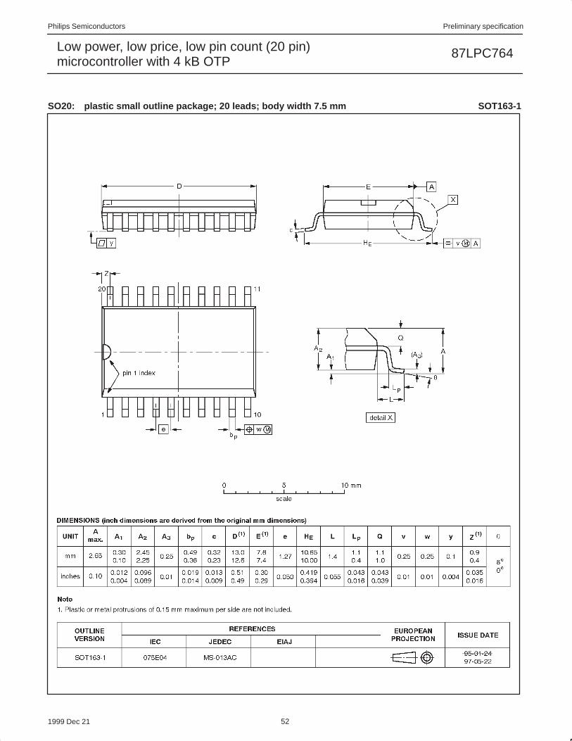
Philips Semiconductors Preliminary specification
87LPC764Low power, low price, low pin count (20 pin)microcontroller with 4 kB OTP
1999 Dec 21 52
SO20: plastic small outline package; 20 leads; body width 7.5 mm SOT163-1

Philips Semiconductors Preliminary specification
87LPC764Low power, low price, low pin count (20 pin)microcontroller with 4 kB OTP
1999 Dec 21 53
NOTES

Philips Semiconductors Preliminary specification
87LPC764Low power, low price, low pin count (20 pin)microcontroller with 4 kB OTP
1999 Dec 21 54
DefinitionsShort-form specification — The data in a short-form specification is extracted from a full data sheet with the same type number and title. Fordetailed information see the relevant data sheet or data handbook.
Limiting values definition — Limiting values given are in accordance with the Absolute Maximum Rating System (IEC 134). Stress above oneor more of the limiting values may cause permanent damage to the device. These are stress ratings only and operation of the device at these orat any other conditions above those given in the Characteristics sections of the specification is not implied. Exposure to limiting values for extendedperiods may affect device reliability.
Application information — Applications that are described herein for any of these products are for illustrative purposes only. PhilipsSemiconductors make no representation or warranty that such applications will be suitable for the specified use without further testing ormodification.
DisclaimersLife support — These products are not designed for use in life support appliances, devices or systems where malfunction of these products canreasonably be expected to result in personal injury. Philips Semiconductors customers using or selling these products for use in such applicationsdo so at their own risk and agree to fully indemnify Philips Semiconductors for any damages resulting from such application.
Right to make changes — Philips Semiconductors reserves the right to make changes, without notice, in the products, including circuits, standardcells, and/or software, described or contained herein in order to improve design and/or performance. Philips Semiconductors assumes noresponsibility or liability for the use of any of these products, conveys no license or title under any patent, copyright, or mask work right to theseproducts, and makes no representations or warranties that these products are free from patent, copyright, or mask work right infringement, unlessotherwise specified.
Philips Semiconductors811 East Arques AvenueP.O. Box 3409Sunnyvale, California 94088–3409Telephone 800-234-7381
Copyright Philips Electronics North America Corporation 1999All rights reserved. Printed in U.S.A.
Date of release: 12-99
Document order number: 9397 750 06708
������ ����������
Data sheetstatus
Objective specification
Preliminary specification
Product specification
Productstatus
Development
Qualification
Production
Definition [1]
This data sheet contains the design target or goal specifications for product development.Specification may change in any manner without notice.
This data sheet contains preliminary data, and supplementary data will be published at a later date.Philips Semiconductors reserves the right to make changes at any time without notice in order toimprove design and supply the best possible product.
This data sheet contains final specifications. Philips Semiconductors reserves the right to makechanges at any time without notice in order to improve design and supply the best possible product.
Data sheet status
[1] Please consult the most recently issued datasheet before initiating or completing a design.