The 8088 & 8086 Microprocessors 4th Ed. by Triebel & Singh net

1
8086/8088 Hardware
Specifications
CEN433
King Saud University
Dr. Mohammed Amer Arafah

Mohammed Amer Arafah2CEN433 - King Saud University
8088/8086 Microprocessors
Fairly old microprocessors, but still considered a good way to introduce the Intel family
Both microprocessors use 16-bit registers and 20-bit address bus (supporting 1 MB memory), but:
- The 8086 (1978): 16-bit external data bus
- The 8088 (1979): 8-bit external data bus
Still used in embedded systems (cost is less than $1)

Mohammed Amer Arafah3CEN433 - King Saud University
Pin Layout of the 8088/8086 Microprocessors

Mohammed Amer Arafah4CEN433 - King Saud University
Pin Layout of the 8088 Microprocessors
Pin budget:
8088, Min mode:
20 Address
8 Data
20 Control & Status
3 Power
51 Total
> 40 pins available
Use multiplexing

Mohammed Amer Arafah5CEN433 - King Saud University
The Modes of Operation
The microprocessors 8086 and 8088 can be configured to work in two modes: The Minimum mode and the Maximum mode.
The Minimum mode is used for single processor system, where 8086/8088 directly generates all the necessary control signals.
The Maximum mode is designed for multiprocessor systems, where an additional “Bus-controller” IC is required to generate the control signals. The processors control the Bus-controller using status-codes.

Mohammed Amer Arafah6CEN433 - King Saud University
The Modes of Operation

Mohammed Amer Arafah7CEN433 - King Saud University
DC Pin Characteristics: Voltages
Standard TTL Output and Inputs Voltage Levels
0 Logic Level
Guaranteed
Output LevelsAccepted
Input Levels
0-Level
Noise Margin
1-Level
Noise Margin
Forbidden
5.0 VVcc
0 Logic Level
1 Logic Level
Forbidden
Region
0 Logic Level
1 Logic Level

Mohammed Amer Arafah8CEN433 - King Saud University
DC Pin Characteristics: CurrentsFan out for a standard TTL output
How many inputs can an output support?
For the 1 logic Level: (output “sources” current)
O/P can source up to
400 A max
I/P sinks
up to 40 A
1Standard
TTL Gate
1-level Fanout = Maximum number of inputs that the output can support
= 400 A/40 A = 10
O/P can sink up to
16 mA max
An I/P sources
up to 1.6 mA
0-level Fanout = Maximum number of inputs that the output can support
= 16 mA/1.6 mA = 10
For the 0 logic Level: (output “sinks” current)
0Standard
TTL Gate

Mohammed Amer Arafah9CEN433 - King Saud University
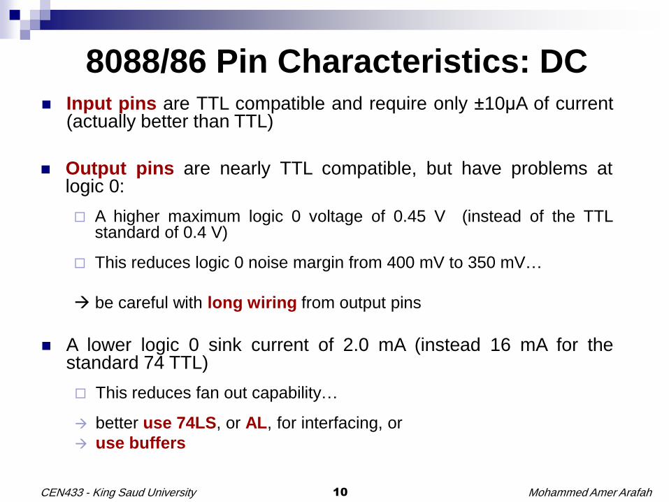
8088/86 Pin Characteristics: DC
Input pins:Output pins:
Guaranteed
Output levelsAccepted
Input levels
0 level noise margin = 0.8 – 0.45 = 0.35 V (8086/88 P)
= 0.8 – 0.40 = 0.40 V (for standard 74 TTL O/P)
0 level fan-out to TTL gate = 2 1.6 1 (8086/88 P)
=16 1.6 = 10 (for standard 74 TTL O/P)
-
* = 16 mA for standard 74 TTL
# = 0.40 V for standard 74 TTL
* = 1.6 mA for standard 74 TTL
# = 40 A for standard 74 TTL
*# *
#
Mohammed Amer Arafah10CEN433 - King Saud University
8088/86 Pin Characteristics: DC Input pins are TTL compatible and require only ±10μA of current
(actually better than TTL)
Output pins are nearly TTL compatible, but have problems atlogic 0:
A higher maximum logic 0 voltage of 0.45 V (instead of the TTLstandard of 0.4 V)
This reduces logic 0 noise margin from 400 mV to 350 mV…
be careful with long wiring from output pins
A lower logic 0 sink current of 2.0 mA (instead 16 mA for thestandard 74 TTL)
This reduces fan out capability…
better use 74LS, or AL, for interfacing, or
use buffers

Mohammed Amer Arafah11CEN433 - King Saud University
Multiplexing
Latch address to a buffer
Data
AD15-0
Address
ALE: Latch address
Write Cycle
For both microprocessors, Address bus
signals are A0-A19 (20 lines) for 1M byte of
addressing space
Data bus signals are
D0-D7 for the 8088
D0-D15 for the 8086
The address & data pins are multiplexed as:
AD0-AD7 (8088)
or AD0-AD15 (8086)
Address/Status pins are MUXed
A/S for A16-19
The ALE O/P signal is used to demultiplex the
address/data (AD) bus and also the
address/status (A/S) bus.
Some functions are multiplexed on the same pins to reduce chip pin count

Mohammed Amer Arafah12CEN433 - King Saud University
The Status (S) Bus
ALE: Latch address and BHE/
Status
8086: Address bits A16-A19 &
BHE/ are muxed with the
status bits S3-S7.
S3 & S4 indicate which segment
register is used with the current
instruction:
S5 = IF (Interrupt flag)
S6 = 0
S7 = 1Spare
S0/, S1/, S2/ are not MUXed. They
encode bus status (current bus
cycle)
Available only in the MAX mode for
use by a bus controller chip
SS0: Not Muxed, Min mode

Mohammed Amer Arafah13CEN433 - King Saud University
Main Control Signals
Common Signals for both MIN and MAX modes:
S0/, The read output (RD/):
indicates a read operation
The write output (WR/) :
indicates a write
The READY input: when low
(not ready), forces the processor
to enter a wait state. Facilitates
interfacing the processor with
slow memory chips

Mohammed Amer Arafah14CEN433 - King Saud University
Main Control Signals (cont’d)
Two hardware interrupt inputs:
INTR input: Hardware interrupt
request. Honored only if the IF flag
is set. The microprocessor enters an
interrupt ACK cycle by lowering the
INTA/ output
NMI input: Hardware non-maskable
interrupt request. Honored
regardless of the status of the IF
flag. Uses interrupt vector 2
TEST/ input: Example: interfacing the
microprocessor with the 8087 math
coprocessor. Checked by the WAIT
instruction that precedes each floating
point instruction. If high, the instruction
waits till input signal goes low and then
gives FP instruction to the math
processor
8086
processor
8087
Math
Coprocessor
TEST/
Synchronizes processor execution
to external events
Test for low

Mohammed Amer Arafah15CEN433 - King Saud University
Main Control Signals (cont’d) CLK input: Basic timing clock for the
processor (Duty cycle= 1/3)
MN/#MX input: Selects either Minimum
(+ 5V directly) or Maximum mode (GND)
#BHE/S7 output (MUXed):
BHE/: (Bus High Enable) Enables
writing to the high byte of the 16-bit
data bus on the 8086
Not on 8088 (has an 8-bit data bus-
no high byte!)
RESET input: resets the microprocessor
(reboots the computer). Causes the
processor to start executing at address
FFFF0H (Start of last 16 bytes of ROM at
the top of the 1MB memory) after
disabling the INTR input interrupts (CLR
IF flag). Input must be kept high for at
least 50 ms. Sampled by the processor at
the + ive clock edge

Mohammed Amer Arafah16CEN433 - King Saud University
Main Control Signals (cont’d)

Mohammed Amer Arafah17CEN433 - King Saud University
Main Control Signals (cont’d)
Mohammed Amer Arafah18CEN433 - King Saud University
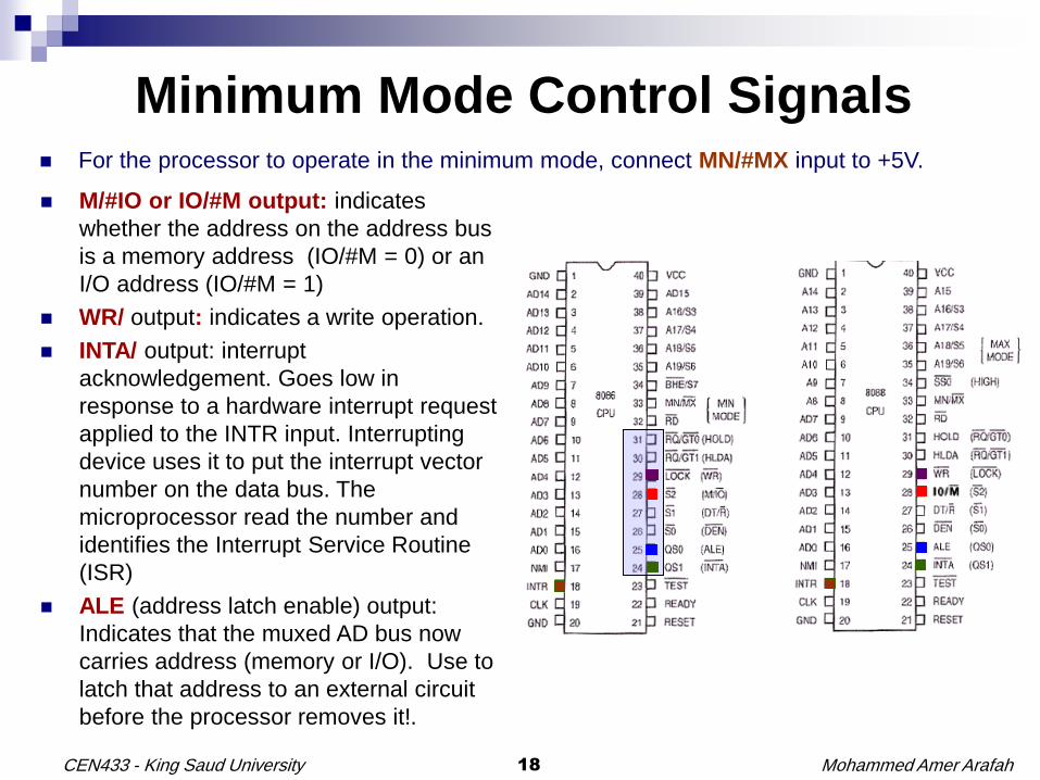
Minimum Mode Control Signals
M/#IO or IO/#M output: indicates
whether the address on the address bus
is a memory address (IO/#M = 0) or an
I/O address (IO/#M = 1)
WR/ output: indicates a write operation.
INTA/ output: interrupt
acknowledgement. Goes low in
response to a hardware interrupt request
applied to the INTR input. Interrupting
device uses it to put the interrupt vector
number on the data bus. The
microprocessor read the number and
identifies the Interrupt Service Routine
(ISR)
ALE (address latch enable) output:
Indicates that the muxed AD bus now
carries address (memory or I/O). Use to
latch that address to an external circuit
before the processor removes it!.
For the processor to operate in the minimum mode, connect MN/#MX input to +5V.
Mohammed Amer Arafah19CEN433 - King Saud University
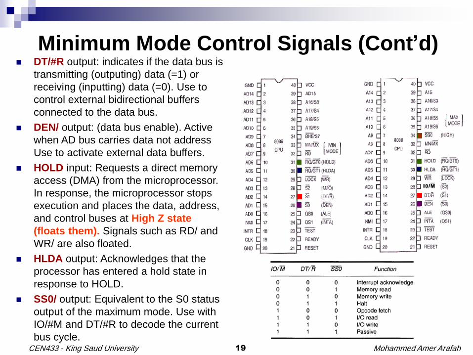
Minimum Mode Control Signals (Cont’d) DT/#R output: indicates if the data bus is
transmitting (outputing) data (=1) or
receiving (inputting) data (=0). Use to
control external bidirectional buffers
connected to the data bus.
DEN/ output: (data bus enable). Active
when AD bus carries data not address
Use to activate external data buffers.
HOLD input: Requests a direct memory
access (DMA) from the microprocessor.
In response, the microprocessor stops
execution and places the data, address,
and control buses at High Z state
(floats them). Signals such as RD/ and
WR/ are also floated.
HLDA output: Acknowledges that the
processor has entered a hold state in
response to HOLD.
SS0/ output: Equivalent to the S0 status
output of the maximum mode. Use with
IO/#M and DT/#R to decode the current
bus cycle.

Mohammed Amer Arafah20CEN433 - King Saud University
Minimum Mode Control Signals (Cont’d)

Mohammed Amer Arafah21CEN433 - King Saud University
Minimum Mode 8088 System

Mohammed Amer Arafah22CEN433 - King Saud University
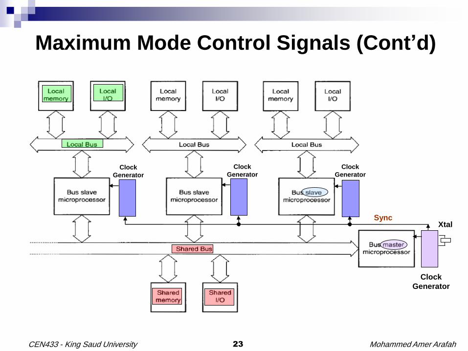
Maximum Mode Control Signals (Cont’d)
S0/, S1/, S2/ outputs: Status bits that
encode the type of the current bus cycle,
Used by the 8288 bus controller and the
8087 coprocessor.
#RQ/GT0, #RQ/GT1: Bidirectional lines
for requesting and granting DMA access
(Request/Get). For use in multiprocessor
systems. The RG/GT0 line has higher
priority.
LOCK/ output: Activated for the duration
of multiprocessor instructions having the
LOCK prefix. Can be used to prevent
other microprocessors from using the
system buses and accessing shared
memory or I/O for the duration of such
instructions, e.g. LOCK:MOV AL,[SI]
QS0, QS1 (Queue Status) outputs:
indicate the status of the internal
instruction queue. For use by the 8087
coprocessor to keep in step
For the processor to operate in the maximum mode, connect MN/#MX input to ground.
Mohammed Amer Arafah23CEN433 - King Saud University
Maximum Mode Control Signals (Cont’d)
Sync
Clock
Generator
Xtal
Clock
Generator
Clock
GeneratorClock
Generator
Mohammed Amer Arafah24CEN433 - King Saud University
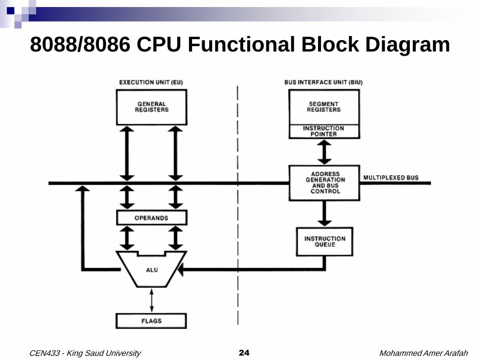
8088/8086 CPU Functional Block Diagram

Mohammed Amer Arafah25CEN433 - King Saud University
8088/8086 CPU Functional Block Diagram

Mohammed Amer Arafah26CEN433 - King Saud University
Internal Architecture of 8088/8086
The 8088/8086 microprocessor has two units: the BusInterface Unit (BIU) and the Execution Unit (EU).
Both units operate simultaneously. This parallelism makes thefetch and execution of instructions independent.
The Bus Interface Unit (BIU) performs all external busoperations, such as instruction fetching, reading/writingoperands from/to memory, and inputting/outputting datafrom/to Input/output peripherals.
The BIU also performs address generation. To perform thisfunction, the BIU contains segment registers, instructionpointers, address generation adder, bus control logic, and aninstruction queue.

Mohammed Amer Arafah27CEN433 - King Saud University
Internal Architecture of 8088/8086
The Execution Unit (EU) performs decoding and execution of instructions.
The EU consists of the arithmetic logic unit (ALU), the FLAGregister, multipurpose registers, and temporary operand register.
The EU accesses instructions from the instruction queue, decodes them, generates operand addresses if necessary, passes the operand addresses to the BIU, requests from the BIU to perform read/write bus cycle from/to memory or I/O peripherals, and performs the operation specified by the instruction on the operands.

Mohammed Amer Arafah28CEN433 - King Saud University
Multipurpose and Special-Purpose Registers
EAX AH AL Accumulator
EBX BH BL Base Index
ECX CH CL Count
EDX DH DL Data
ESP SP Stack Pointer
EBP BP Base Pointer
EDI DI Destination Index
ESI SI Source Index
EIP IP Instruction Pointer
EFLAGS FLAGS Flags
AX
BX
CX
DX
Multipurpose and Special-Purpose Registers
of the Intel 8086 through the Pentium
32-bit
names
16-bit
names
8-bit
names

Mohammed Amer Arafah29CEN433 - King Saud University
Multipurpose and Special-Purpose Registers
All general registers of the 8088 microprocessor can be used for arithmetic and logic operations. The general registers are:
Accumulator register consists of 2 8-bit registers AL and AH, which can be combined together and used as a 16-bit register AX. Accumulator can be used for I/O operations and string manipulation.
Base register consists of 2 8-bit registers BL and BH, which can be combined together and used as a 16-bit register BX. BX register usually contains a data pointer used for based, based indexed or register indirect addressing.
Count register consists of 2 8-bit registers CL and CH, which can be combined together and used as a 16-bit register CX. Count register can be used as a counter in string manipulation and shift/rotate instructions.
Data register consists of 2 8-bit registers DL and DH, which can be combined together and used as a 16-bit register DX. Data register can be used as a port number in I/O operations. In integer 32-bit multiply and divide instruction the DX register contains high-order word of the initial or resulting number.
The following registers are both general and index registers:
Stack Pointer (SP) is a 16-bit register pointing to program stack.
Base Pointer (BP) is a 16-bit register pointing to data in stack segment. BP register is usually used for based, based indexed or register indirect addressing.
Source Index (SI) is a 16-bit register. SI is used for indexed, based indexed and register indirect addressing, as well as a source data address in string manipulation instructions.
Destination Index (DI) is a 16-bit register. DI is used for indexed, based indexed and register indirect addressing, as well as a destination data address in string manipulation instructions.
Other registers:
Instruction Pointer (IP) is a 16-bit register.
Flag Register

Mohammed Amer Arafah30CEN433 - King Saud University
The Flag Register
O D I T S Z A P C
CARRY
PARITY
AUXILLARY CARRY
ZERO
SIGN
OVERFLOW
INTERRUPT-ENABLE
DIRECTION
TRAP
TF DF IF OF SF ZF AF PF CF
Control
Flags
Status
Flags

Mohammed Amer Arafah31CEN433 - King Saud University
The Flag Register Overflow Flag (OF) - set if the result is too large positive number, or is too
small negative number to fit into destination operand.
Direction Flag (DF) - if set (STD) then string manipulation instructions will auto-decrement index registers. If cleared (CLD) then the index registers will be auto-incremented.
Interrupt-enable Flag (IF) - setting this bit (STI) enables maskable interrupts. Clearing this bit (CLI) disables maskable interrupts.
Single-step Flag (TF) - if set then single-step interrupt will occur after the next instruction.
Sign Flag (SF) - set if the most significant bit of the result is set.
Zero Flag (ZF) - set if the result is zero.
Auxiliary carry Flag (AF) - set if there was a carry from or borrow to bits 0-3 in the AL register.
Parity Flag (PF) - set if parity (the number of "1" bits) in the low-order byte of the result is even.
Carry Flag (CF) - set if there was a carry from or borrow to the most significant bit during last result calculation.

Mohammed Amer Arafah32CEN433 - King Saud University
Segment Registers
There are four different 64 KB segments for instructions, stack, data and extra data. To specify where in 1 MB of processor memory these 4 segments are located the processor uses four segment registers:
Code segment (CS) is a 16-bit register containing address of 64 KB segment with processor instructions. The processor uses CS segment for all accesses to instructions referenced by instruction pointer (IP) register.
Stack segment (SS) is a 16-bit register containing address of 64KB segment with program stack. By default, the processor assumes that all data referenced by the stack pointer (SP) and base pointer (BP) registers is located in the stack segment.
Data segment (DS) is a 16-bit register containing address of 64KB segment with program data. By default, the processor assumes that all data referenced by general registers (AX, BX, CX, DX) and index register (SI, DI) is located in the data segment.
Extra segment (ES) is a 16-bit register containing address of 64KB segment, usually with program data. By default, the processor assumes that the DI register references the ES segment in string manipulation instructions.
CS Code
SS Stack
DS Data
ES Extra

Mohammed Amer Arafah33CEN433 - King Saud University
Real Mode Memory Addressing
0 0 0 0Offset Value
015
Segment Value
015
0 0 0 0
Adder
20- bit Physical Memory Address
019F 0 0 0
Code Segment (CS)
00000
FFFFF
64K- byte
Segment
F0000
IP = 500HF0500
Real Mode Memory
Mohammed Amer Arafah34CEN433 - King Saud University
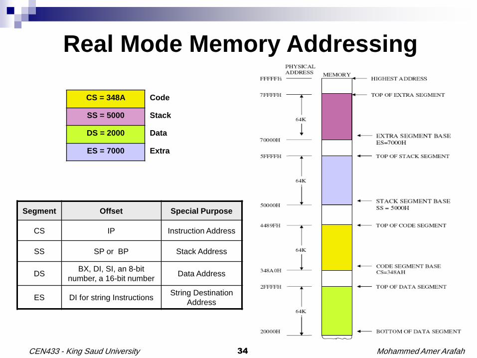
Real Mode Memory Addressing
CS = 348A Code
SS = 5000 Stack
DS = 2000 Data
ES = 7000 Extra
Segment Offset Special Purpose
CS IP Instruction Address
SS SP or BP Stack Address
DSBX, DI, SI, an 8-bit
number, a 16-bit numberData Address
ES DI for string InstructionsString Destination
Address

Mohammed Amer Arafah35CEN433 - King Saud University
Real Mode Memory Addressing
FFFFF
FE000F E 0 0
Code Segment (CS)
IP = 0020HFE020Code
Segment
Example 1:
CS = FE00H
IP = 0020H
Physical Address = FE020H
Example 2:
MOV AX, 4000H
MOV DS, AX
MOV BX, 1000H
MOV AL, [BX] 4FFFF
400004000
Data Segment (DS)
BX = 1000H41000 55
Data
Segment
55 AL
Example 3:
MOV AX, 4000H
MOV DS, AX
MOV AL, 33H
MOV BX, 0300H
MOV [BX], AL4FFFF
400004000
Data Segment (DS)
BX = 0300H40300 33
Data
Segment
33 AL

Mohammed Amer Arafah36CEN433 - King Saud University
Real Mode Memory AddressingExample 4:
MOV AX, 6000H
MOV DS, AX
MOV SI, 5H
MOV AL, [SI] 6FFFF
600006000
Data Segment (DS)
SI = 0005H60005 AA
Data
Segment
AA AL
Example 5:
MOV AX, 8000H
MOV DS, AX
MOV AL, 77H
MOV [300], AL 8FFFF
800008000
Data Segment (DS)
Offset = 0300H80300 77
Data
Segment
77 AL
Example 6:
MOV AX, 8000H
MOV DS, AX
MOV AL, [200]8FFFF
800008000
Data Segment (DS)
Offset = 0200H80200 22
Data
Segment
22 AL
Mohammed Amer Arafah37CEN433 - King Saud University
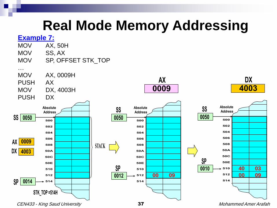
Real Mode Memory AddressingExample 7:MOV AX, 50H
MOV SS, AX
MOV SP, OFFSET STK_TOP
…
MOV AX, 0009H
PUSH AX
MOV DX, 4003H
PUSH DX
00 09 00 09
40 03

Mohammed Amer Arafah38CEN433 - King Saud University
Real Mode Memory Addressing
Example 8:MOV AX, 50H
MOV SS, AX
MOV SP, OFFSET STK_TOP
…
POP DX
POP AX
00 0900 09
40 03

Mohammed Amer Arafah39CEN433 - King Saud University
Real Mode Memory Addressing
Example 10:
MOV AX, 5000H
MOV SS, AX
MOV BP, 14H
MOV AL, [BP] 5FFFF
500005000
Stack Segment (SS)
BP = 0014H50014 11
Stack
Segment
11 AL
Example 9:
MOV AX, 5000H
MOV SS, AX
MOV BP, 14H
MOV [BP], AL 5FFFF
500005000
Stack Segment (SS)
BP = 0014H50014 11
Stack
Segment
11 AL

Mohammed Amer Arafah40CEN433 - King Saud University
Structure of Assembly ProgramsNAME PROJECT
DATA SEGMENT AT 40H
ORG 0H
VAR1 DB ?
VAR2 DB ?
DATA ENDS
;------------------------------------------------
STACK SEGMENT AT 50H
DW 10 DUP(?)
STK_TOP LABEL WORD
STACK ENDS
;------------------------------------------------
EPROM SEGMENT AT 0FE00H
ASSUME CS:EPROM, DS:DATA, SS:STACK
ORG 0H
BEGIN LABEL FAR
MOV AX, DATA
MOV DS, AX
EPROM ENDS
;-------------------------------------------------
CODE SEGMENT AT 0FFFFH
ASSUME CS:CODE, SS:STACK
ORG 0H
START: CLI
MOV AX,STACK
MOV SS,AX
MOV SP,OFFSET STK_TOP
JMP BEGIN
CODE ENDS
END START

Mohammed Amer Arafah41CEN433 - King Saud University
RAM Mapping
Odd Addresses Even Addresses Physical Address
00000
… … …
… … …
003FF
VAR2 VAR1 00400
…
1 00500
2 00502
3 00504
4 00506
5 00508
6 0050A
7 0050C
8 0050E
9 00510
10 00512
00514
…
007FF
0014 SP
0040 DATA
0050 STACK
Interrupt
Vector
Table
Data
Segment
Stack
Segment

Mohammed Amer Arafah42CEN433 - King Saud University
Stack Segment

Mohammed Amer Arafah43CEN433 - King Saud University
ExampleNAME PROJECT
DATA SEGMENT AT 40H
ORG 0H
VAR1 DB 5H
VAR2 DB 6H
VAR3 DB ?
DATA ENDS
;------------------------------------------------
STACK SEGMENT AT 50H
DW 10 DUP(?)
STK_TOP LABEL WORD
STACK ENDS
;------------------------------------------------
EPROM SEGMENT AT 0FE00H
ASSUME CS:EPROM, DS:DATA, SS:STACK
ORG 0H
BEGIN LABEL FAR
MOV AX, DATA
MOV DS, AX
MOV AL, VAR1
ADD AL, VAR2
MOV VAR3, AL
AGAIN: JMP AGAIN
EPROM ENDS
;-------------------------------------------------
CODE SEGMENT AT 0FFFFH
ASSUME CS:CODE, SS:STACK
ORG 0H
START: CLI
MOV AX,STACK
MOV SS,AX
MOV SP,OFFSET STK_TOP
JMP BEGIN
CODE ENDS
END START

Mohammed Amer Arafah44CEN433 - King Saud University
Example (Cont’d)
Odd Addresses Even Addresses Physical Address
00000
… … …
… … …
003FF
VAR2 = 6H VAR1 = 5H 00400
VAR3 = ? …
1 00500
2 00502
3 00504
4 00506
5 00508
6 0050A
7 0050C
8 0050E
9 00510
10 00512
00514
…
007FF
0014 SP
0040
DATA
0050
STACK
Interrupt
Vector
Table
Data
Segment
Stack
Segment
5HAL
5HVAR1
BHALAdding VAR2
to AL
6HVAR2
+
BHVAR3
Description Value
DS 40H
SS 50H
STK_TOP 514H
SP 14H
Absolute Address of VAR1 400H
Absolute Address of VAR3 402H
Value stored in VAR3 after
executing the program
BH
EPROM Size 8KB

Mohammed Amer Arafah45CEN433 - King Saud University
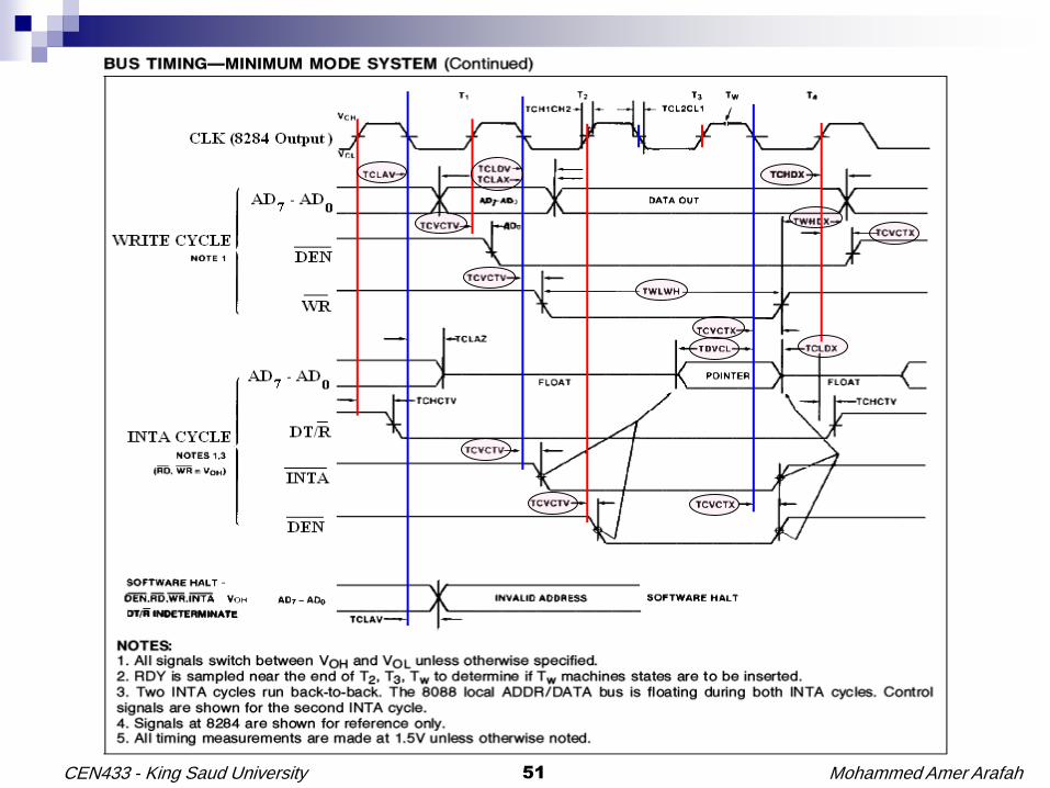
Bus Timing
Clock Cycle
A data transfer operation to/from
the microprocessor occupies at
least one bus cycle
Each bus cycle consists of 4
clock cycles, T1, T2, T3, T4,
each of period T
With 5 MHz processor clock:
T = 1/5 MHz = 0.2 ms
Bus cycle = 4 T = 0.8 ms
Max rate for memory and I/O
transactions = 1/0.8 = 1.25 M
operations per sec (Fetch
speed).
Processor executes 2.5 Million
Instructions per sec (MIPS)
(Execute speed)

Mohammed Amer Arafah46CEN433 - King Saud University
Timing Waveforms (Read Bus Cycle)

Mohammed Amer Arafah47CEN433 - King Saud University
Timing Waveforms (Write Bus Cycle)

Mohammed Amer Arafah48CEN433 - King Saud University

Mohammed Amer Arafah49CEN433 - King Saud University

Mohammed Amer Arafah50CEN433 - King Saud University
Mohammed Amer Arafah51CEN433 - King Saud University

Mohammed Amer Arafah52CEN433 - King Saud University
The 8088 Timing Parameters

Mohammed Amer Arafah53CEN433 - King Saud University
The 8088 Timing Parameters

Mohammed Amer Arafah54CEN433 - King Saud University
Minimum Mode 8088 System

Mohammed Amer Arafah55CEN433 - King Saud University
The 8088-2 Timing Waveforms (Minimum Mode)
nsTCLAZ 5010 nsTDVCL 20 nsTCLDX 10
nsTCLAV 6010 nsTCHDX 10
nsTCLRL 10010 nsTCLRH 8010
nsTCLCL 500125 nsTCLCH 68 nsTCHCL 44
nsTCLLH 50 nsT CHLL 55

Mohammed Amer Arafah56CEN433 - King Saud University
Interfacing EPROM to 8088-2
DECODERLATCHSELECTCHIP ttnsT 60_
nsTCLRL 10010 nsTCLRH 8010
nsTCLCL 500125 nsTCLCH 68 nsTCHCL 44
nsTCLAV 6010 nsTCLAZ 5010 nsTDVCL 20 nsTCLDX 10
nsTCLLH 50 nsT CHLL 55
TOUTPUT_ENABLE ≤ tT1+ 100ns + tOR
LATCHAddressBuffered tnsT 60_
Mohammed Amer Arafah57CEN433 - King Saud University
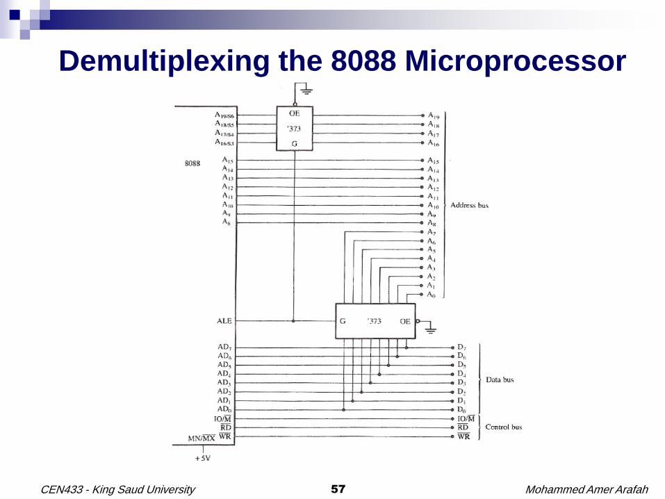
Demultiplexing the 8088 Microprocessor

Mohammed Amer Arafah58CEN433 - King Saud University
Fully Buffered 8088 Microprocessor

Mohammed Amer Arafah59CEN433 - King Saud University
Demultiplexing the 8086 Microprocessor
Mohammed Amer Arafah60CEN433 - King Saud University
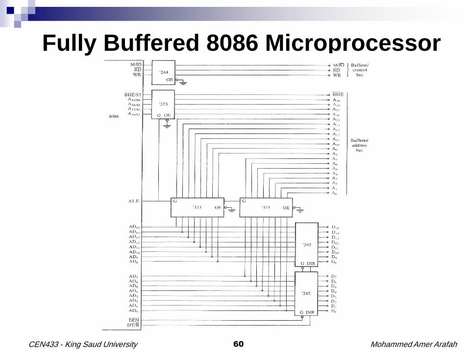
Fully Buffered 8086 Microprocessor

Mohammed Amer Arafah61CEN433 - King Saud University
Buffering Since the microprocessor output pins provide minimum drive current at the
0 logic level, buffering is often needed if more TTL loads are connected to
any bus signal: Consider 3 types of signals.
For demuxed signals: Latches used for demuxing, e.g. ‘373, can also
provide the buffering for the demuxed lines:
0-level output can sink up to 32 mA (20 x 1.6 mA loads)
1-Level output can source up to 5.2 mA (1 load = 40 mA)
For non-demuxed unidirectional (always output) address and control signals
(e.g. A8-15 on the 8088), buffering is required- often using the 74ALS244
(unidirectional) buffer.
For non-demuxed bidirectional data signals (pin used for both in and out),
buffering is often accomplished with the 74ALS245 bidirectional bus buffer.
Caution: Buffering introduces a small delay in the buffered signals. This is
acceptable unless memory or I/O devices operate close to the maximum
bus speed

Mohammed Amer Arafah62CEN433 - King Saud University

Mohammed Amer Arafah63CEN433 - King Saud University

Mohammed Amer Arafah64CEN433 - King Saud University

Mohammed Amer Arafah65CEN433 - King Saud University

Mohammed Amer Arafah66CEN433 - King Saud University

Mohammed Amer Arafah67CEN433 - King Saud University


![Weeks 12 and 13 Interrupt Interface of the 8088 and 8086 ...alkar/ELE414/dirz2005/w12-414-[2005].pdf · Weeks 12 and 13 Interrupt Interface of the 8088 and 8086 Microprocessors 2](https://static.fdocuments.in/doc/165x107/5b5acf5f7f8b9a24038d4677/weeks-12-and-13-interrupt-interface-of-the-8088-and-8086-alkarele414dirz2005w12-414-2005pdf.jpg)
![Weeks 12 and 13 Interrupt Interface of the 8088 and 8086 ...alkar/EE212/week12[2006].pdf · Interrupt Interface of the 8088 and 8086 Microprocessors . 2 ... • Data are input from](https://static.fdocuments.in/doc/165x107/5b5ac7e37f8b9a885b8caa1c/weeks-12-and-13-interrupt-interface-of-the-8088-and-8086-alkaree212week122006pdf.jpg)