8086 Microprocessors & Peripherals - · PDF fileRead / Write timing diagrams, ... Procedures,...
16
Transcript of 8086 Microprocessors & Peripherals - · PDF fileRead / Write timing diagrams, ... Procedures,...

1
8086 Microprocessors & Peripherals
(06IT/BM - 52)
Sessions handled
by
Prof. M.V. SREENIVAS RAO. GSSSIETW, MYSORE
Prof. M. SHIVAKUMAR. BIET, DAVANGERE
Prof. VAGEESH.V.KANTLI. BIET, DAVANGERE
2
8086 MICROPROCESSOR AND PERIPHERALS (06IT52)
PART - A UNIT 1
Introduction, Microprocessor based computer system, Architecture of 8086
Microprocessor, Pin functions, Minimum / Maximum mode of operation.
UNIT 2
Read / Write timing diagrams, 8086 instruction set, Instruction template for
data transfer instruction, addressing modes.
UNIT 3
Assembler directives, Programming examples.
UNIT 4
Linking and relocation, Stacks, Procedures, Interrupt and Interrupt routines, Macros.
PART – B
UNIT 5
DOS interrupt 21H function to read a character from keyboard, Write character to
console, Creation of a new file, read/write from/to file, Serial / parallel communication.
Interfacing devices, Memory devices and interfacing.
UNIT 6
8055 PPI device and interfacing, keyboard, display, ADC, DAC, Stepper motor and
Printer interfacing using 8255.
UNIT 7
8279 programmable keyboard/display controller and interfacing, 8253 and interfacing,
8259 programmable interrupt controller and interfacing.
UNIT 8
8257 DMA controller and interfacing, serial communication using 8251 & 8087 Numeric
data processor and interfacing, RS 232 serial communication standards.
3
TEXTBOOKS:
1 Advanced Microprocessor and Peripherals- A.K.Ray and K.M. Bhurchandi,
Tata McGraw Hill.
2 Microcomputer systems 8086/8088 family, Architecture, Programming and
Design - Yu-Cheng Liu & Glenn A Gibson, 2nd
Edition- July 2003, Prentice
Hall of India.
REFERENCE BOOKS:
1. Microprocessor and Interfacing, Programming & Hardware- Douglas V
Hall, 2nd
Edition, Tata McGraw Hill .
2. Microprocessor Architecture, Programming and Applications with the 8085-
Ramesh S Gaonkar, 4th
Edition, Penram International.
4
Unit 1
Introduction:
Microprocessor:
It is a semiconductor device consisting of electronic logic circuits manufactured
by using either a Large scale (LSI) or Very Large Scale (VLSI) Integration Technique. It
includes the ALU, register arrays and control circuits on a single chip.
The microprocessor has a set of instructions, designed internally, to manipulate
data and communicate with peripherals. This process of data manipulation and
communication is determined by the logic design of the microprocessor called the
architecture.
The era microprocessors in the year 1971, the Intel introduced the first 4-bit
microprocessor is 4004. Using this the first portable calculator is designed. The following
table1 shows the list of Intel microprocessors.
Table 1
Year Name Bit Size
1971 4004 4
1972 8008 8
1974 8080 8
1977 8085 8
1978 8086 16
1979 8089 16
1982 80286 32
1985 80386 32
1989 80486 32
1993 80586(Pentium) 32
1995 Pentium Pro 32
1997 Pentium II 32
1999 Ecleron and Pentium III 32
2000 Pentium IV 32
2001 Intanium 64
2003 Pentium M processor 64
2005 Pentium IV and Xeon 64
2006 Pentium D 900 64
5
The different manufacturing companies are introduced different bit size microprocessors
in the past decade is shown in the table 2
Table 2
A microcomputer system just as any other computer system, include two principal
components Hardware and Software. The hardware is a course the circuitry, cabinetry etc
and the software is the collection of programs which direct the computer while it
performs its tasks.
The memory is used to store both data and instructions that are currently being
used. It is normally broken into several modules, each module containing several
thousand locations. Each location may contain part or all of a datum or instruction and is
associated with an identifier called a memory address. The CPU does its work by
successfully inputting, or fetching instructions from memory and carrying out the tasks
detected them.
Company Name Processor Name
AMD Athlon
Cypress CY7C601
DEC ALPHA
Fujitsu MBL8086
Harris CS80C286
LSI Logic LR 30000
National
Semiconductor
NS321016N
SGS-Thomson ST6X86
SUN-Micro SRP1030
Texas
Instruments
TMS390
Toshiba TC85R4000
Zilog Z80
Motorola 68000
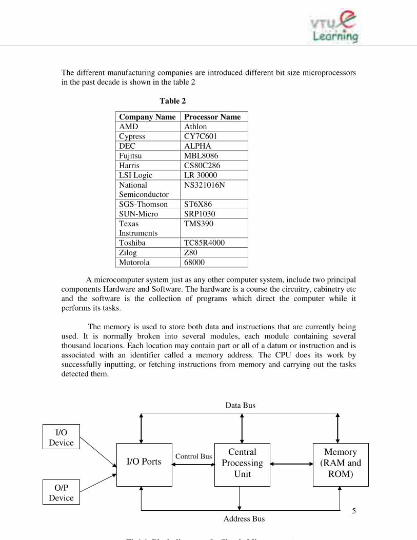
I/O Ports Central
Processing
Unit
Memory
(RAM and
ROM)
I/O
Device
O/P
Device
Data Bus
Control Bus
Address Bus
Fig1.1. Block diagram of a Simple Microcomputer
6
Figure1.1 shows block diagram of a simple microcomputer. The major parts are
the central processing unit or CPU, memory and the input and output circuitry or
Input/output. Connecting these parts are three sets of parallel line is called buses and
control bus. In a microcomputer the CPU is a microprocessor and is often referred to as
the microprocessor unit (MPU). Its purpose is to decode the instruction and use them to
control the activity with in the system. It performs all arithmetic and logical
computations.
Memory: Memory section usually consists of a mixture of RAM and ROM. It may also
magnetic floppy disks, magnetic hard disks or optical disks, to store the data.
Input/output: The input/output section allows the computer to take in data from the
outside world or send data to the outside world. Peripherals such as keyboards, video
display terminals. Printers and modem are connected to the input/output section. These
allow the user and computer to communicate with each other. The actual physical devices
used to interface the computer buses to external systems are often called ports. An
input/output port allows data from keyboard, an analog to digital converter (ADC) or
some other source to be read into the computer under the control of the CPU. An output
port is used to send data from the computer to some peripheral, such as a video display
terminal, a printer or a digital to analog converter (DAC).
Central processing Unit (CPU): CPU controls the operation of the computer .In a
microcomputer the CPU is a microprocessor. The CPU fetches the binary coded
instructions from memory, decodes the instructions into a series of simple action and
carries out these actions in sequence of steps.
CPU contains an a address counter or instruction pointer register which holds the
address of the next instruction or data item to be fetched from memory, general purpose
register, which are used for temporary storage or binary data and circuitry, which
generates the control bus signals.
Address bus: The address bus consists of 16, 20, 24 or 32 parallel lines. On these lines
the CPU sends out the address of the memory locations that are to be written to or read
from. The number of memory locations that the CPU can addresses is determined by the
number of address lines, then it can directly address 2n memory location. When the CPU
reads data from or writes data to a port, it sends the port address on the address bus.
Ex: CPU has 16 address lines can address 216
or 65536 memory locations.
Data bus: It consists of 8, 16, 32 parallel signal lines. The data bus lines are
bidirectional. This means that the CPU can read, data from memory or from a port on
these lines, or it can send data out to memory or to port on these lines.
Control bus: The control bus consists of 4 to 10 parallel signals lines. The CPU sends
out signals on the control bus enable the outputs of addressed memory devices or port
7
devices. Typical control bus signal are memory read, memory write, I/O read and I/O
write.
Hardware, software and Firmware: hardware is the given to the physical devices and
circuitry of the computer. Software refers to collection of programs written for the
computer. Firmware is the term given programs stored in ROM’s or in other devices
which permanently keep their stored information.
Introduction to 16-bit Microprocessor:
The 16-bit Microprocessor families are designed primarily to complete with
microcomputers and are oriented towards high-level languages. Their applications
sometimes overlap those of the 8-bit microprocessors. The have powerful instruction sets
and capable of addressing mega bytes of memory.
The era of 16-bit Microprocessors began in 1974 with the introduction of PACE
chip by National Semiconductor. The Texas Instruments TMS9900 was introduced in the
year 1976. The Intel 8086 commercially available in the year 1978, Zilog Z800 in the
year 1979, The Motorola MC68000 in the year 1980.
The 16-bit Microprocessors are available in different pin packages.
Ex: Intel 8086/8088 40 pin package
Zilog Z8001 40 pin package
Digital equipment LSI-II 40 pin package
Motorola MC68000 64 pin package
National Semiconductor NS16000 48 pin package
The primary objectives of this 16-bit Microprocessor can be summarized as follows.
1. Increase memory addressing capability
2. Increase execution speed
3. Provide a powerful instruction set
4. Facilitate programming in high-level languages.
The INTEL iAPX 8086/8088:
It is a 16-bit Microprocessor housed in a 40-pin Dual-Inline-Package (DIP) and
capable of addressing 1Megabyte of memory, various versions of this chip can operate
with different clock frequencies
i. 8086 (5 MHz)
ii.8086-2 (8 MHz)
iii. 8086-1 (10 MHz).
It contains approximately 29,000 transistors and is fabricated using the HMOS
technology . The term 16-bit means that its arithmetic logic unit, its internal registers and
most of its instructions are designed to work with 16-bit binary word. The 8086
Microprocessor has a 16-bit data bus, so it can read from or write data to memory and
ports either 16-bits or 8-bits at a time. The 8086 Microprocessor has 20-bit address bus,
so it can address any one of 220 or 1,048,576 memory locations. Here 16-bit words will
be stored in two consecutive memory locations. If the first byte of a word is at an even
address, the 8086 can read entire word in one operation, If the first byte of the word is at
an odd address the 8086 will read the first byte with one bus operation and the second
8
byte with another bus operation.
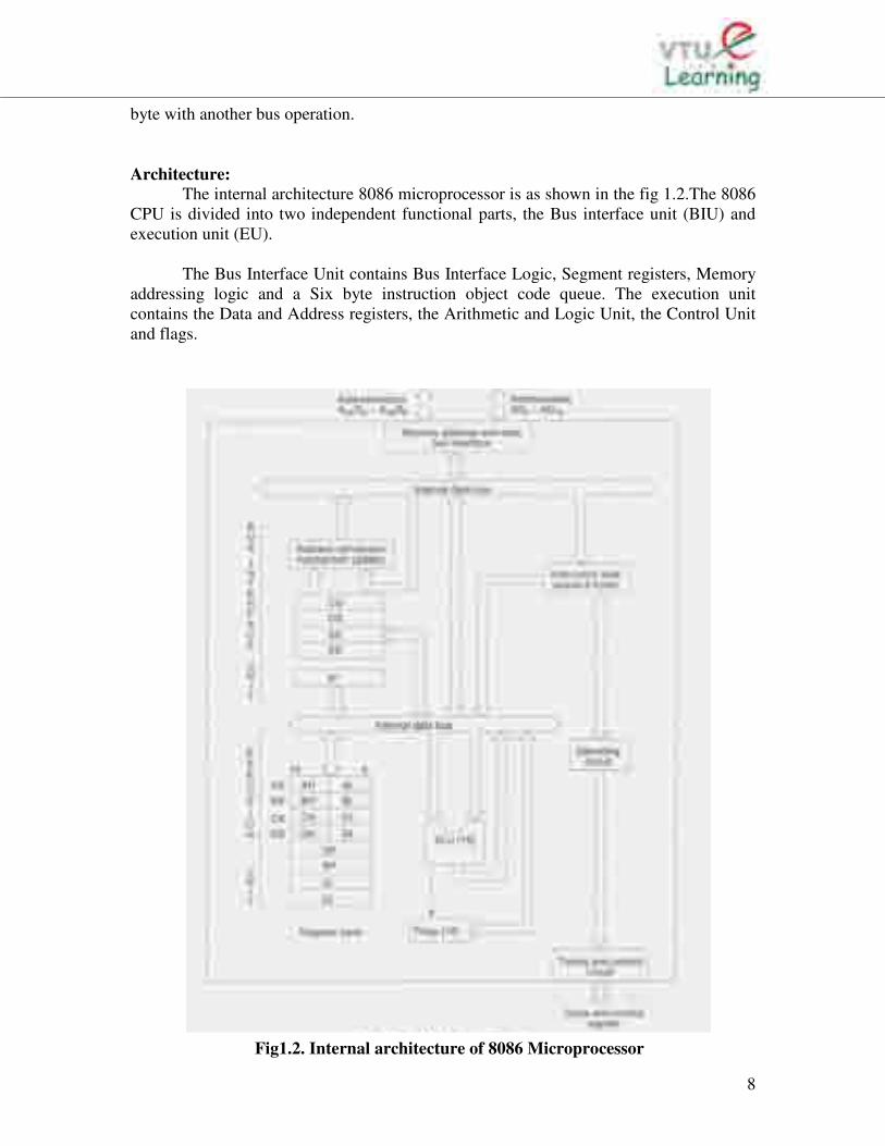
Architecture:
The internal architecture 8086 microprocessor is as shown in the fig 1.2.The 8086
CPU is divided into two independent functional parts, the Bus interface unit (BIU) and
execution unit (EU).
The Bus Interface Unit contains Bus Interface Logic, Segment registers, Memory
addressing logic and a Six byte instruction object code queue. The execution unit
contains the Data and Address registers, the Arithmetic and Logic Unit, the Control Unit
and flags.
Fig1.2. Internal architecture of 8086 Microprocessor
9
The BIU sends out address, fetches the instructions from memory, read data from
ports and memory, and writes the data to ports and memory. In other words the BIU
handles all transfers of data and addresses on the buses for the execution unit.
The execution unit (EU) of the 8086 tells the BIU where to fetch instructions or
data from, decodes instructions and executes instruction. The EU contains control
circuitry which directs internal operations. A decoder in the EU translates instructions
fetched from memory into a series of actions which the EU carries out. The EU is has a
16-bit ALU which can add, subtract, AND, OR, XOR, increment, decrement,
complement or shift binary numbers. The EU is decoding an instruction or executing an
instruction which does not require use of the buses.
The Queue: The BIU fetches up to 6 instruction bytes for the following instructions. The
BIU stores these prefetched bytes in first-in-first-out register set called a queue. When the
EU is ready for its next instruction it simply reads the instruction byte(s) for the
instruction from the queue in the BIU. This is much faster than sending out an address to
the system memory and waiting for memory to send back the next instruction byte or
bytes. Except in the case of JMP and CALL instructions, where the queue must be
dumped and then reloaded starting from a new address, this prefetch-and-queue scheme
greatly speeds up processing. Fetching the next instruction while the current instruction
executes is called pipelining.
Word Read
Each of 1 MB memory address of 8086 represents a byte wide location.16-bit
words will be stored in two consecutive memory locations. If first byte of the data is
stored at an even address, 8086 can read the entire word in one operation.
For example if the 16 bit data is stored at even address 00520H is 9634H
MOV BX, [00520H]
8086 reads the first byte and stores the data in BL and reads the 2nd
byte and stores the
data in BH
BL= (00520H) i.e. BL=34H
BH= (00521H) BH=96H
If the first byte of the data is stored at an odd address, 8086 needs two operations to read
the 16 bit data.
For example if the 16 bit data is stored at even address 00521H is 3897H
MOV BX, [00521H]
In first operation, 8086 reads the 16 bit data from the 00520H location and stores the data
of 00521H location in register BL and discards the data of 00520H location In 2nd
operation, 8086 reads the 16 bit data from the 00522H location and stores the data of
00522H location in register BH and discards the data of 00523H location.
BL= (00521H) i.e. BL=97H
BH= (00522H) BH=38H
10
Byte Read:
MOV BH, [Addr]
For Even Address:
Ex: MOV BH, [00520H]
8086 reads the first byte from 00520 location and stores the data in BH and reads the 2nd
byte from the 00521H location and ignores it
BH =[ 00520H]
For Odd Address
MOV BH, [Addr]
Ex: MOV BH, [00521H]
8086 reads the first byte from 00520H location and ignores it and reads the 2nd byte from
the 00521 location and stores the data in BH
BH = [00521H]
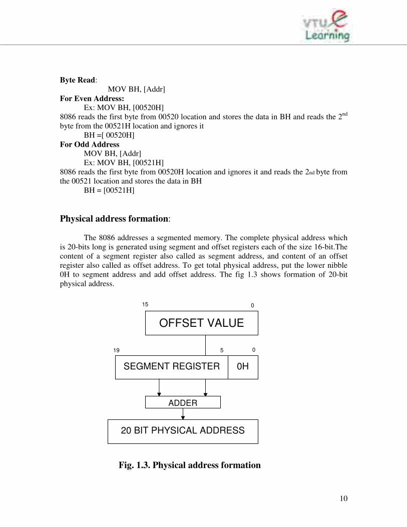
Physical address formation:
The 8086 addresses a segmented memory. The complete physical address which
is 20-bits long is generated using segment and offset registers each of the size 16-bit.The
content of a segment register also called as segment address, and content of an offset
register also called as offset address. To get total physical address, put the lower nibble
0H to segment address and add offset address. The fig 1.3 shows formation of 20-bit
physical address.
OFFSET VALUE
SEGMENT REGISTER 0H
ADDER
20 BIT PHYSICAL ADDRESS
15 0
5 0 19
Fig. 1.3. Physical address formation

11
Register organization of 8086:
8086 has a powerful set of registers containing general purpose and special
purpose registers. All the registers of 8086 are 16-bit registers. The general purpose
registers, can be used either 8-bit registers or 16-bit registers. The general purpose
registers are either used for holding the data, variables and intermediate results
temporarily or for other purpose like counter or for storing offset address for some
particular addressing modes etc. The special purpose registers are used as segment
registers, pointers, index registers or as offset storage registers for particular addressing
modes. Fig 1.4 shows register organization of 8086. We will categorize the register set
into four groups as follows:
General data registers:
The registers AX, BX, CX, and DX are the general 16-bit registers.
AX Register: Accumulator register consists of two 8-bit registers AL and AH, which
can be combined together and used as a 16- bit register AX. AL in this case contains the
low-order byte of the word, and AH contains the high-order byte. Accumulator can be
used for I/O operations, rotate and string manipulation.
BX Register: This register is mainly used as a base register. It holds the starting base
location of a memory region within a data segment. It is used as offset storage for
forming physical address in case of certain addressing mode.
CX Register: It is used as default counter or count register in case of string and loop
instructions.
DX Register: Data register can be used as a port number in I/O operations and implicit
operand or destination in case of few instructions. In integer 32-bit multiply and divide
instruction the DX register contains high-order word of the initial or resulting number.
AH
BH
CH
AL
BL
CL
DL DH
BX
DX
AX
CX
General data registers
CS
SS
DS
ES
Segment registers
FLAGS/PSW
SP
IP
DI
SI
BP
Pointers and index registers
Fig.1.4 Register organization of 8086 Microprocessor
12
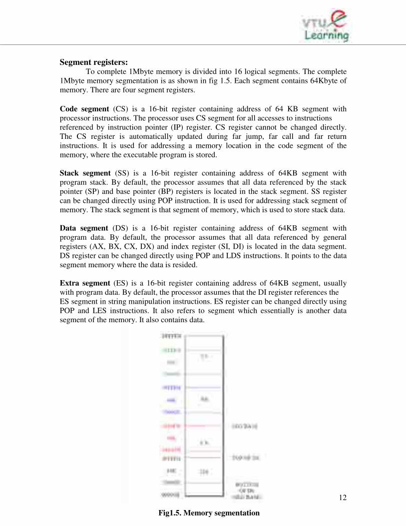
Segment registers: To complete 1Mbyte memory is divided into 16 logical segments. The complete
1Mbyte memory segmentation is as shown in fig 1.5. Each segment contains 64Kbyte of
memory. There are four segment registers.
Code segment (CS) is a 16-bit register containing address of 64 KB segment with
processor instructions. The processor uses CS segment for all accesses to instructions
referenced by instruction pointer (IP) register. CS register cannot be changed directly.
The CS register is automatically updated during far jump, far call and far return
instructions. It is used for addressing a memory location in the code segment of the
memory, where the executable program is stored.
Stack segment (SS) is a 16-bit register containing address of 64KB segment with
program stack. By default, the processor assumes that all data referenced by the stack
pointer (SP) and base pointer (BP) registers is located in the stack segment. SS register
can be changed directly using POP instruction. It is used for addressing stack segment of
memory. The stack segment is that segment of memory, which is used to store stack data.
Data segment (DS) is a 16-bit register containing address of 64KB segment with
program data. By default, the processor assumes that all data referenced by general
registers (AX, BX, CX, DX) and index register (SI, DI) is located in the data segment.
DS register can be changed directly using POP and LDS instructions. It points to the data
segment memory where the data is resided.
Extra segment (ES) is a 16-bit register containing address of 64KB segment, usually
with program data. By default, the processor assumes that the DI register references the
ES segment in string manipulation instructions. ES register can be changed directly using
POP and LES instructions. It also refers to segment which essentially is another data
segment of the memory. It also contains data.
Fig1.5. Memory segmentation
13
Pointers and index registers.
The pointers contain within the particular segments. The pointers IP, BP, SP
usually contain offsets within the code, data and stack segments respectively
Stack Pointer (SP) is a 16-bit register pointing to program stack in stack segment.
Base Pointer (BP) is a 16-bit register pointing to data in stack segment. BP register is
usually used for based, based indexed or register indirect addressing.
Source Index (SI) is a 16-bit register. SI is used for indexed, based indexed and register
indirect addressing, as well as a source data addresses in string manipulation instructions.
Destination Index (DI) is a 16-bit register. DI is used for indexed, based indexed and
register indirect addressing, as well as a destination data address in string manipulation
instructions.
Flag register
Flags Register determines the current state of the processor. They are modified
automatically by CPU after mathematical operations, this allows to determine the type of
the result, and to determine conditions to transfer control to other parts of the program.
The 8086 flag register as shown in the fig 1.6. 8086 has 9 active flags and they are
divided into two categories:
1. Conditional Flags
2. Control Flags
Conditional Flags
Conditional flags are as follows:
Carry Flag (CY): This flag indicates an overflow condition for unsigned integer
arithmetic. It is also used in multiple-precision arithmetic.
Auxiliary Flag (AC): If an operation performed in ALU generates a carry/barrow from
lower nibble (i.e. D0 – D3) to upper nibble (i.e. D4 – D7), the AC flag is set i.e. carry given
by D3 bit to D4 is AC flag. This is not a general-purpose flag, it is used internally by the
X X X X OF DF IF TF SF ZF X AC X PF X CY
15 14 12 13 11 10 9 8 7 6 5 4 3 2 1 1
Fig1.6 . Flag Register of 8086
X = Undefined
14
Processor to perform Binary to BCD conversion.
Parity Flag (PF): This flag is used to indicate the parity of result. If lower order 8-bits of
the result contains even number of 1’s, the Parity Flag is set and for odd number of 1’s,
the Parity flag is reset.
Zero Flag (ZF): It is set; if the result of arithmetic or logical operation is zero else it is
reset.
Sign Flag (SF): In sign magnitude format the sign of number is indicated by MSB bit. If
the result of operation is negative, sign flag is set.
Control Flags
Control flags are set or reset deliberately to control the operations of the execution unit.
Control flags are as follows:
Trap Flag (TF): It is used for single step control. It allows user to execute one
instruction of a program at a time for debugging. When trap flag is set, program can be
run in single step mode.
Interrupt Flag (IF): It is an interrupt enable/disable flag. If it is set, the maskable
interrupt of 8086 is enabled and if it is reset, the interrupt is disabled. It can be set by
executing instruction sit and can be cleared by executing CLI instruction.
Direction Flag (DF): It is used in string operation. If it is set, string bytes are accessed
from higher memory address to lower memory address. When it is reset, the string bytes
are accessed from lower memory address to higher memory address.


![Weeks 12 and 13 Interrupt Interface of the 8088 and 8086 ...alkar/ELE414/dirz2005/w12-414-[2005].pdf · Weeks 12 and 13 Interrupt Interface of the 8088 and 8086 Microprocessors 2](https://static.fdocuments.in/doc/165x107/5b5acf5f7f8b9a24038d4677/weeks-12-and-13-interrupt-interface-of-the-8088-and-8086-alkarele414dirz2005w12-414-2005pdf.jpg)

![Weeks 4-5 8088/8086 Microprocessor Programmingalkar/ELE414/dirz2005/w4-414-[2005].pdf · 8088/8086 Microprocessor Programming . 2 ... 80x86 Interrupts • An interrupt is an event](https://static.fdocuments.in/doc/165x107/5e70a945fb5d632d193db492/weeks-4-5-80888086-microprocessor-alkarele414dirz2005w4-414-2005pdf-80888086.jpg)