8085-A brief description
112
The features of INTEL 8085 are : • It is an 8 bit processor. • It is a single chip N-MOS device with 40 pins. • It has multiplexed address and data bus.(AD0-AD7). • It works on 5 Volt dc power supply. • The maximum clock frequency is 3 MHz while minimum frequency is 500kHz. • It provides 74 instructions with 5 different addressing modes.
-
Upload
pujit-juneja -
Category
Documents
-
view
38 -
download
2
Transcript of 8085-A brief description
The features of INTEL 8085 are :
• It is an 8 bit processor.
• It is a single chip N-MOS device with 40 pins.
• It has multiplexed address and data bus.(AD0-AD7).
• It works on 5 Volt dc power supply.
• The maximum clock frequency is 3 MHz while minimum frequency is 500kHz.
• It provides 74 instructions with 5 different addressing modes.
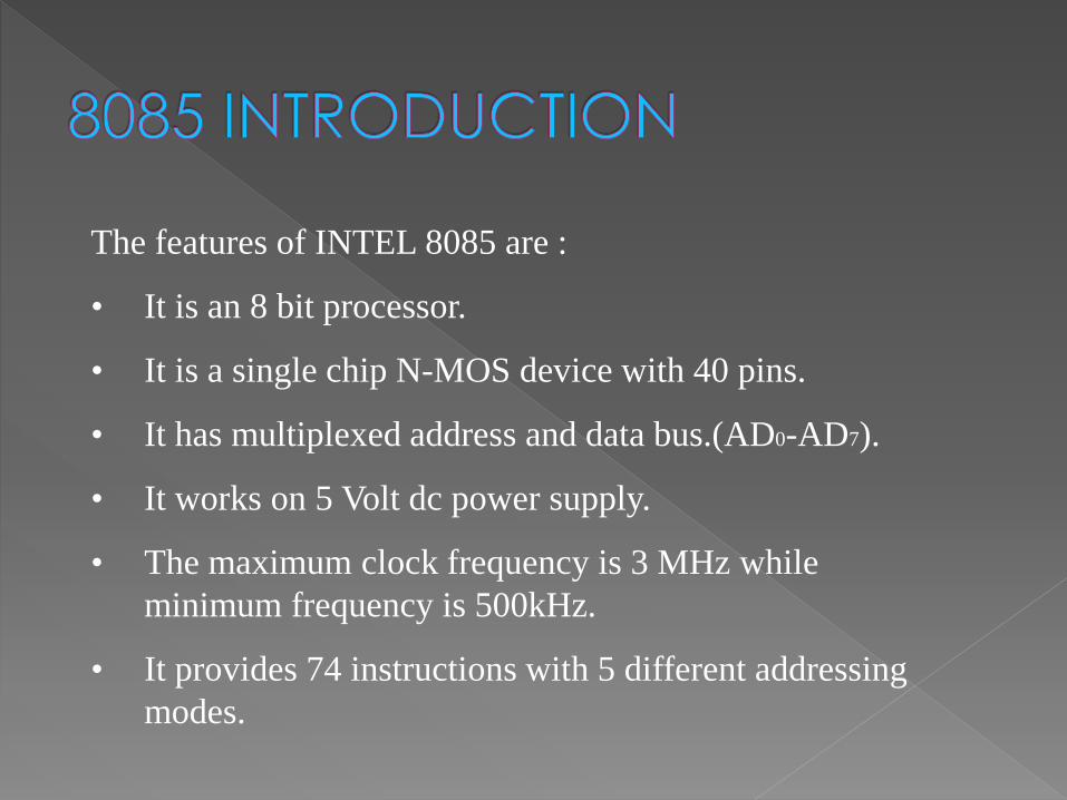
It provides 16 address lines so it can access 2^16 =64K bytes of memory.
It generates 8 bit I/O address so it can access 2^8=256 input ports.
It provides 5 hardware interrupts:TRAP, RST 5.5, RST 6.5, RST 7.5,INTR.
It provides Acc ,one flag register ,6 general purpose registers and two special purpose registers(SP,PC).
It provides serial lines SID ,SOD.So serial peripherals can be interfaced with 8085 directly.

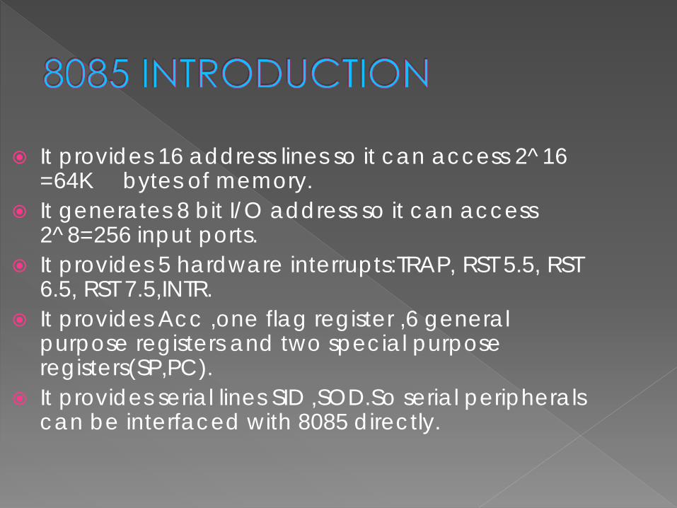
Some important pins are : AD0-AD7: Multiplexed Address and data lines. A8-A15: Tri-stated higher order address lines. ALE: Address latch enable is an output signal.It
goes high when operation is started by processor . S0,S1: These are the status signals used to indicate
type of operation. RD¯: Read is active low input signal used to read
data from I/O device or memory. WR¯:Write is an active low output signal used write
data on memory or an I/O device.

READY:This an output signal used to check the status of output device.If it is low, µP will WAIT until it is high.
TRAP:It is an Edge triggered highest priority , non mask able interrupt. After TRAP, restart occurs and execution starts from address 0024H.
RST5.5,6.5,7.5:These are maskable interrupts and have low priority than TRAP.
INTR¯&INTA:INTR is a interrupt request signal after which µP generates INTA or interrupt acknowledge signal.
IO/M¯:This is output pin or signal used to indicate whether 8085 is working in I/O mode(IO/M¯=1) or Memory mode(IO/M¯=0 ).
HOLD&HLDA:HOLD is an input signal .When µP receives HOLD signal it completes current machine cycle and stops executing next instruction.In response to HOLD µP generates HLDA that is HOLD Acknowledge signal.
RESET IN¯:This is input signal.When RESET IN¯ is low µp restarts and starts executing from location 0000H.
SID: Serial input data is input pin used to accept serial 1 bit data .
X1X2 :These are clock input signals and are connected to external LC,or RC circuit.These are divide by two so if 6 MHz is connected to X1X2, the operating frequency becomes 3 MHz.
VCC&VSS:Power supply VCC=+ -5Volt& VSS=-GND reference.
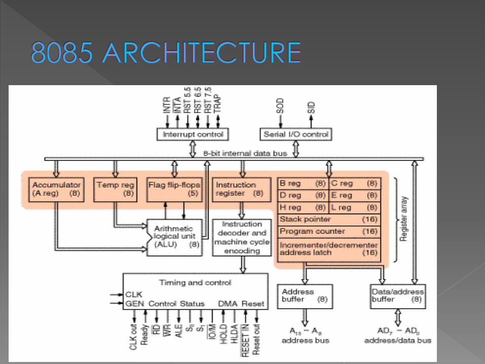

Accumulator: It is 8 bit general purpose register. It is connected to ALU. So most of the operations are done in Acc. Temporary register: It is not available for user All the arithmetic and logical operations are done
in the temporary register but user can’t access it. Flag: It is a group of 5 flip flops used to know status of
various operations done. The Flag Register along with Accumulator is called
PSW or Program Status Word.
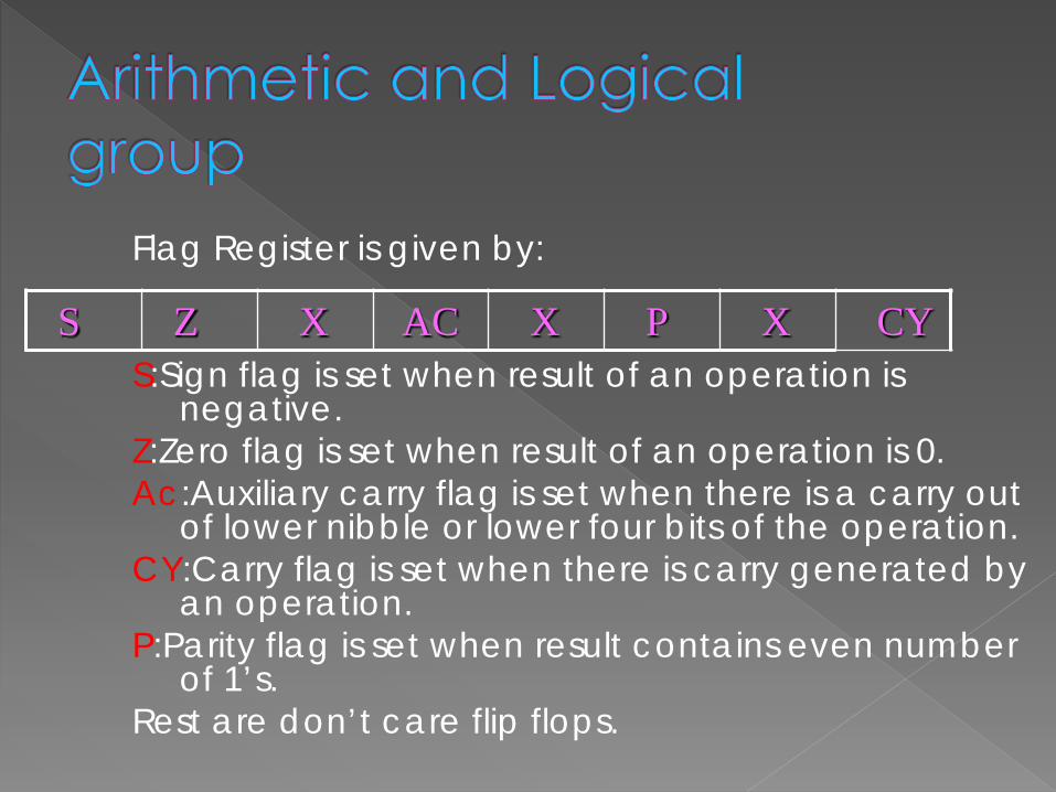
Flag Register is given by: S:Sign flag is set when result of an operation is
negative. Z:Zero flag is set when result of an operation is 0. Ac:Auxiliary carry flag is set when there is a carry out
of lower nibble or lower four bits of the operation. CY:Carry flag is set when there is carry generated by
an operation. P:Parity flag is set when result contains even number
of 1’s. Rest are don’t care flip flops.
S Z X AC X P X CY

Temporary registers (W,Z):These are not available for user. These are loaded only when there is an operation being performed.
General purpose:There are six general purpose registers in 8085 namely B,C,D,E,H,L.These are used for various data manipulations.
Special purpose :There are two special purpose registers in 8085:
1. SP :Stack Pointer. 2. PC:Program Counter.
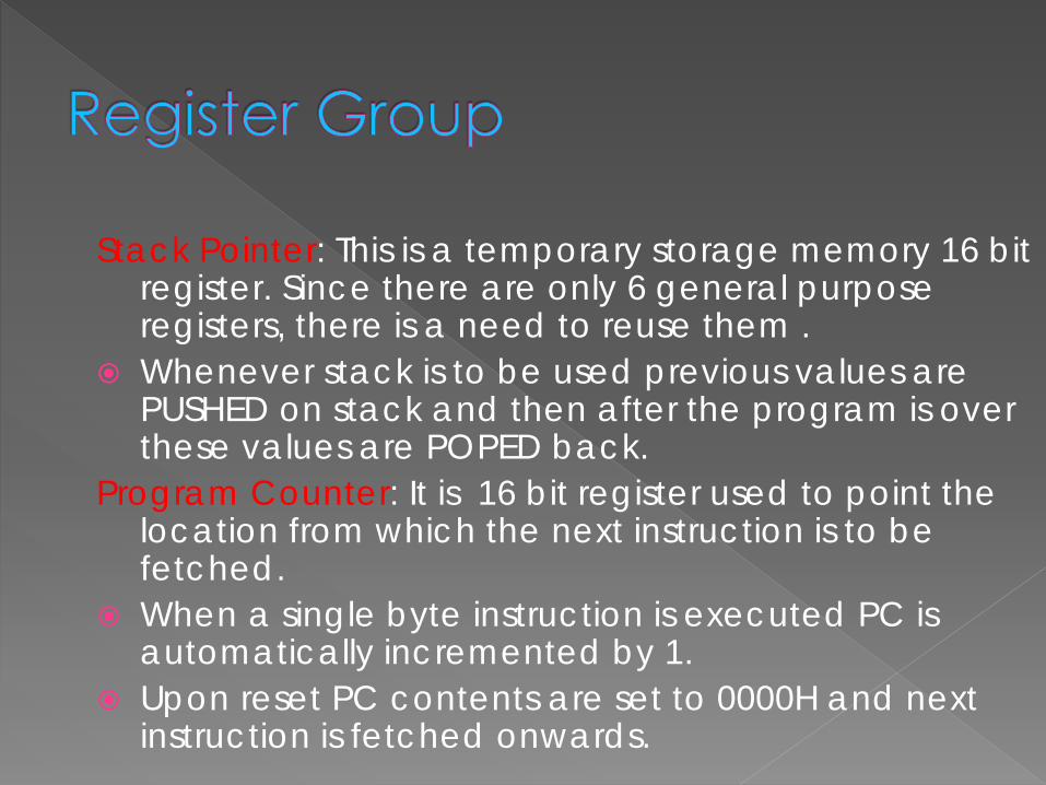
Stack Pointer: This is a temporary storage memory 16 bit register. Since there are only 6 general purpose registers, there is a need to reuse them .
Whenever stack is to be used previous values are PUSHED on stack and then after the program is over these values are POPED back.
Program Counter: It is 16 bit register used to point the location from which the next instruction is to be fetched.
When a single byte instruction is executed PC is automatically incremented by 1.
Upon reset PC contents are set to 0000H and next instruction is fetched onwards.
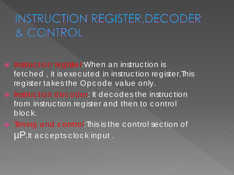
Instruction register:When an instruction is fetched , it is executed in instruction register.This register takes the Opcode value only.
Instruction decoder: It decodes the instruction from instruction register and then to control block.
Timing and control:This is the control section of µP.It accepts clock input .
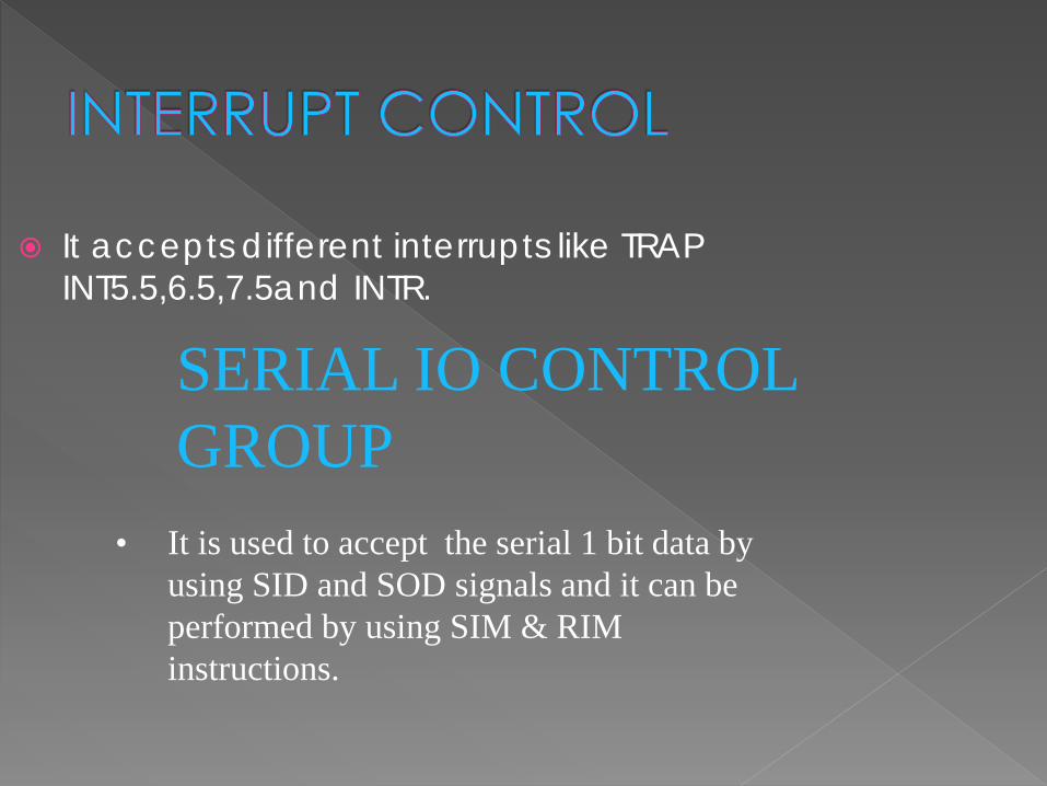
It accepts different interrupts like TRAP INT5.5,6.5,7.5and INTR.
SERIAL IO CONTROL GROUP
• It is used to accept the serial 1 bit data by using SID and SOD signals and it can be performed by using SIM & RIM instructions.
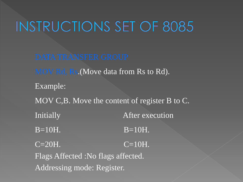
DATA TRANSFER GROUP
MOV Rd, Rs.(Move data from Rs to Rd).
Example:
MOV C,B. Move the content of register B to C.
Initially After execution
B=10H. B=10H.
C=20H. C=10H. Flags Affected :No flags affected. Addressing mode: Register.
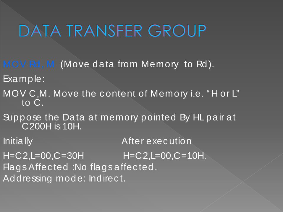
MOV Rd, M (Move data from Memory to Rd). Example: MOV C,M. Move the content of Memory i.e. “H or L”
to C. Suppose the Data at memory pointed By HL pair at
C200H is 10H. Initially After execution H=C2,L=00,C=30H H=C2,L=00,C=10H. Flags Affected :No flags affected. Addressing mode: Indirect.
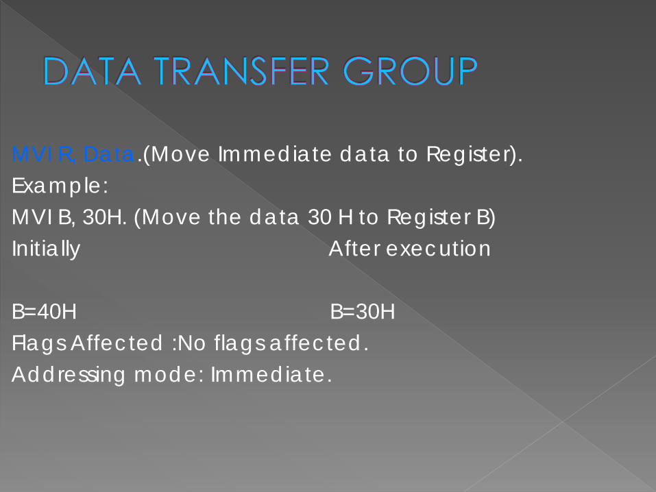
MVI R, Data.(Move Immediate data to Register). Example: MVI B, 30H. (Move the data 30 H to Register B) Initially After execution B=40H B=30H Flags Affected :No flags affected. Addressing mode: Immediate.
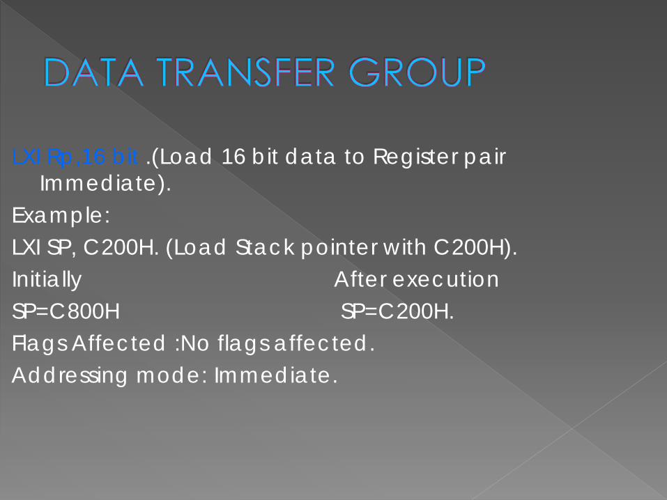
LXI Rp,16 bit .(Load 16 bit data to Register pair Immediate).
Example: LXI SP, C200H. (Load Stack pointer with C200H). Initially After execution SP=C800H SP=C200H. Flags Affected :No flags affected. Addressing mode: Immediate.
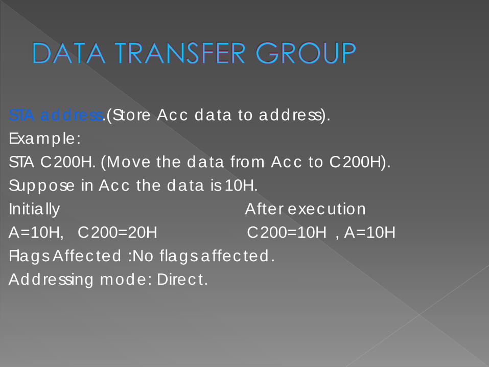
STA address.(Store Acc data to address). Example: STA C200H. (Move the data from Acc to C200H). Suppose in Acc the data is 10H. Initially After execution A=10H, C200=20H C200=10H , A=10H Flags Affected :No flags affected. Addressing mode: Direct.

LHLD address.(Load HL pair with data from address). Example: LHLD C200H. (Move the data from C200 to HL pair). Suppose at C200 the data is 20H,30H . Initially After execution H=10H,L=20H H=20H,L=30H. C2=20H,00=30H C2=20H,00=30H Flags Affected :No flags affected. Addressing mode: Direct.
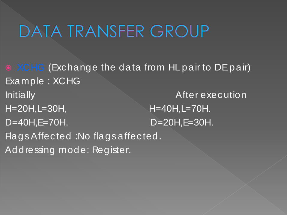
XCHG (Exchange the data from HL pair to DE pair) Example : XCHG Initially After execution H=20H,L=30H, H=40H,L=70H. D=40H,E=70H. D=20H,E=30H. Flags Affected :No flags affected. Addressing mode: Register.

IN 8 bit address (Move the data from address to Acc) Example: IN 80H Move the data from 80H port address to
Accumulator. Suppose data at 80H is 39H. Initially After execution A=20H. A=39H Flags Affected :No flags affected. Addressing mode: Direct.

OUT 8 bit address (Move the data from Acc to address)
Example: OUT 80H Move the data from Acc to port address 80H. Suppose data at Acc is 39H. Initially After execution A=39H. 80=10H. A=39H,80=39H. Flags Affected :No flags affected. Addressing mode: Direct.
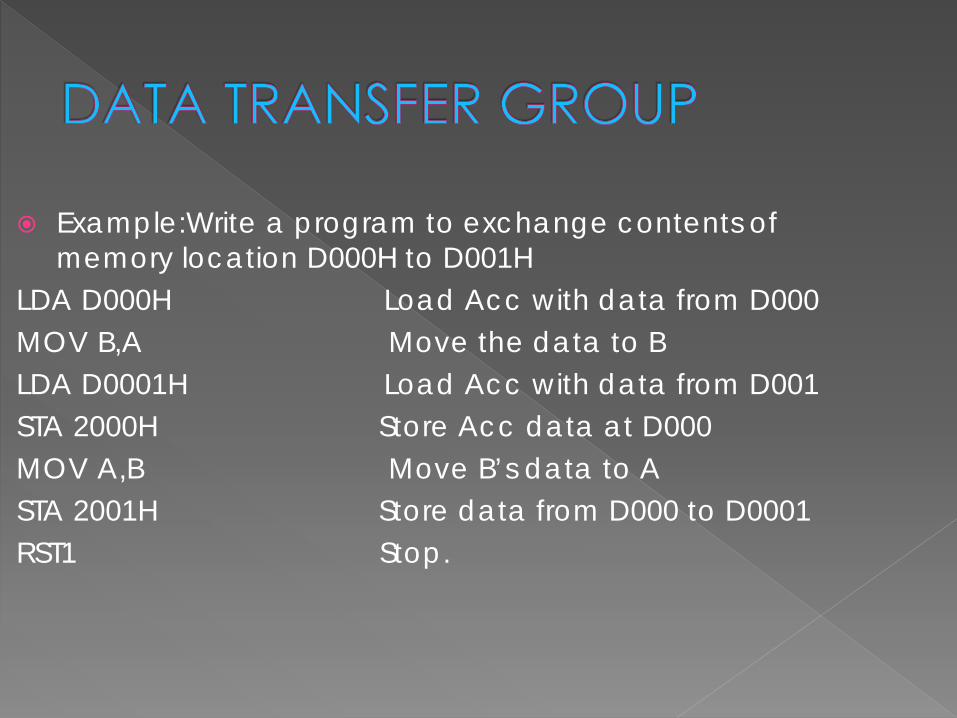
Example:Write a program to exchange contents of memory location D000H to D001H
LDA D000H Load Acc with data from D000 MOV B,A Move the data to B LDA D0001H Load Acc with data from D001 STA 2000H Store Acc data at D000 MOV A,B Move B’s data to A STA 2001H Store data from D000 to D0001 RST1 Stop.
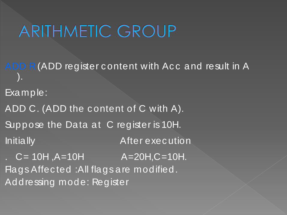
ADD R (ADD register content with Acc and result in A ).
Example: ADD C. (ADD the content of C with A). Suppose the Data at C register is 10H. Initially After execution . C= 10H ,A=10H A=20H,C=10H. Flags Affected :All flags are modified. Addressing mode: Register

ADD M(ADD H or L Reg content with Acc and result in A ).
Example: ADD M. (ADD the content of HL with A). Suppose the Data at memory pointed by HL
register 1020H is 10H. Initially After execution . H= 10H ,L=20H . H=10H,L=20H. A=20H,C=10H. A=30H. Flags Affected :All flags are modified. Addressing mode: Register Indirect.
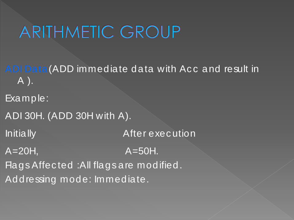
ADI Data(ADD immediate data with Acc and result in A ).
Example:
ADI 30H. (ADD 30H with A).
Initially After execution
A=20H, A=50H. Flags Affected :All flags are modified. Addressing mode: Immediate.
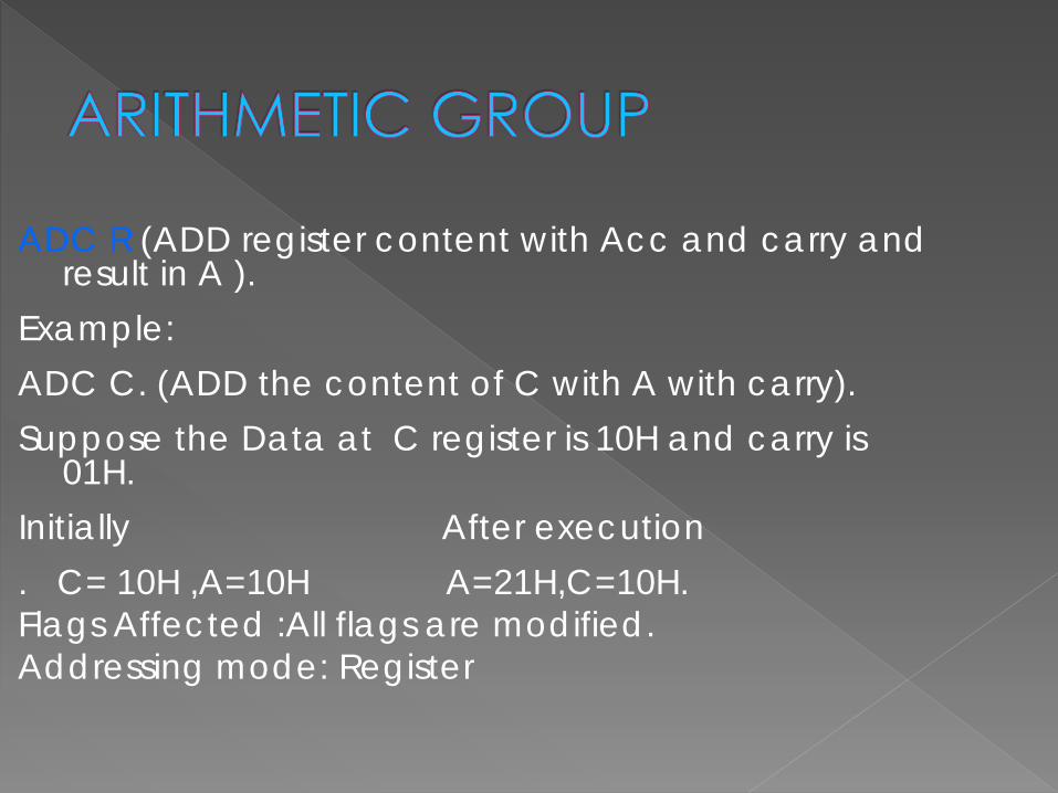
ADC R (ADD register content with Acc and carry and result in A ).
Example: ADC C. (ADD the content of C with A with carry). Suppose the Data at C register is 10H and carry is
01H. Initially After execution . C= 10H ,A=10H A=21H,C=10H. Flags Affected :All flags are modified. Addressing mode: Register

Example: Write a program to perform 16 bit addition of 1234H& 4321H. Store answer at H & L registers.
MVI B,21H B=21H MVI A,34H A=34H MVI C,43H C=43H MVI D,12H D=12H ADD B A=34+21H MOV L,A L=55H MOV A,C A=43H ADC D A=43+12H MOV H,A H=55H RST1 STOP.

SUB R (Subtract register content from Acc and result in A ).
Example: SUB B. (Subtract the content of B from A ). Suppose the Data at B register is 10H . Initially After execution . B= 10H ,A=20H A=10H,B=10H. Flags Affected :All flags are modified. Addressing mode: Register

SBB R (Subtract register content from Acc with borrow and result in A ).
Example: SBB B. (Subtract the content of B from A with borrow). Suppose the Data at B register is 10H and borrow is
01H . Initially After execution . B= 0FH ,A=20H A=10H,B=0FH. Flags Affected :All flags are modified. Addressing mode: Register

SUI Data(Subtract immediate data from Acc and result in A ).
Example:
SUI 30H. (Subtract 30H from A).
Initially After execution
A=80H, A=50H. Flags Affected :All flags are modified. Addressing mode: Immediate
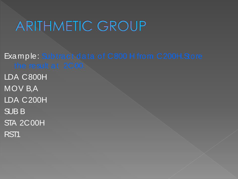
Example: Subtract data of C800 H from C200H.Store the result at 2C00.
LDA C800H MOV B,A LDA C200H SUB B STA 2C00H RST1

DAD Rp (Add specified register pair with HL pair) Example:DAD D.(Add the content of E with L and
that of D with H register and result in HL pair) Suppose the content of HL pair is H=20H ,L=40H
and DE pair is D=30H, E=10H. Initially After execution H=20H ,L=40H H=50H ,L=50H D=30H, E=10H D=30H, E=10H Flags Affected :Only carry flag is modified. Addressing mode: Register.

DAA (Decimal adjust accumulator) Example: MVI A,12H ADI 39H DAA . This instruction is used to store result in BCD form.If
lower nibble is greater than 9 ,6 is added while if upper nibble is greater than 9,6 is added to it to get BCD result.
Initially After execution 12+39=4B 12+39=51 in BCD form. Flags Affected :All flags are modified. Addressing mode: Register

INR R (Increment register content by 1 ). Example: INR C. (Increment the content of C by 1). Suppose the Data at C register is 10H. Initially After execution C= 10H C=11H. Flags Affected :All flags are modified except carry
flag. Addressing mode: Register.

DCR R (Decrement register content by 1 ). Example: DCR C. (Decrement the content of C by 1). Suppose the Data at C register is 10H. Initially After execution C= 10H C=0FH. Flags Affected :All flags are modified except carry
flag. Addressing mode: Register.
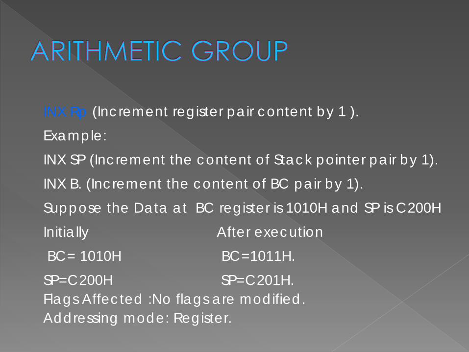
INX Rp (Increment register pair content by 1 ). Example: INX SP (Increment the content of Stack pointer pair by 1). INX B. (Increment the content of BC pair by 1). Suppose the Data at BC register is 1010H and SP is C200H Initially After execution BC= 1010H BC=1011H. SP=C200H SP=C201H. Flags Affected :No flags are modified. Addressing mode: Register.
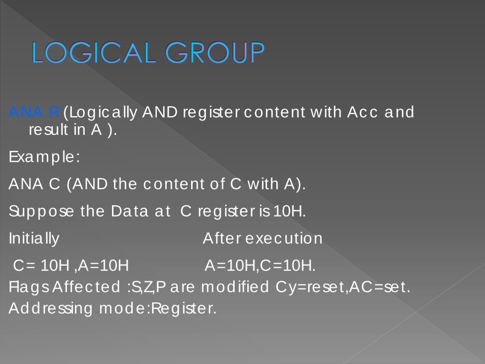
ANA R (Logically AND register content with Acc and result in A ).
Example: ANA C (AND the content of C with A). Suppose the Data at C register is 10H. Initially After execution C= 10H ,A=10H A=10H,C=10H. Flags Affected :S,Z,P are modified Cy=reset,AC=set. Addressing mode:Register.
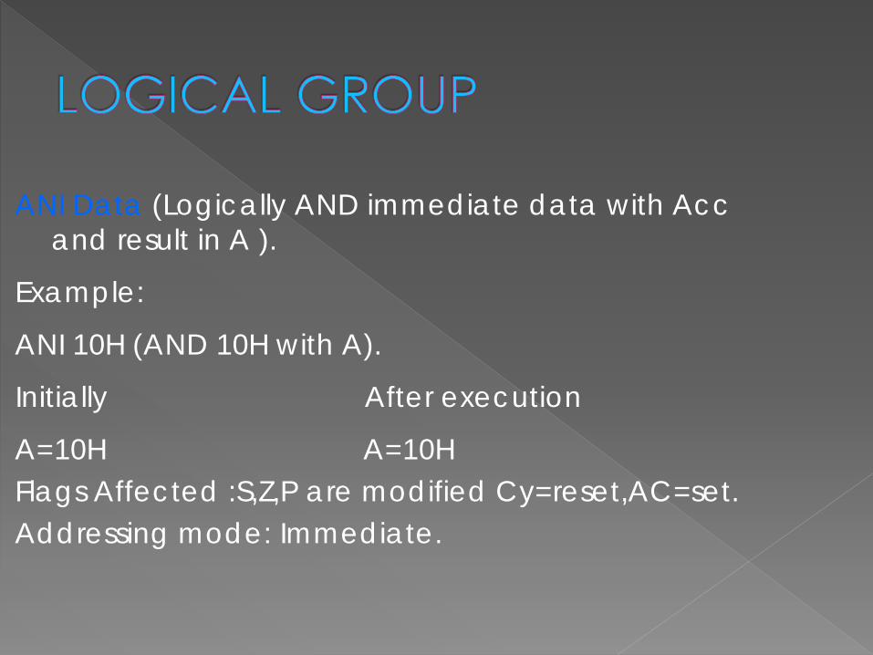
ANI Data (Logically AND immediate data with Acc and result in A ).
Example:
ANI 10H (AND 10H with A).
Initially After execution
A=10H A=10H Flags Affected :S,Z,P are modified Cy=reset,AC=set. Addressing mode: Immediate.

ORA R (Logically OR register content with Acc and result in A5 ).
Example: ORA C (OR the content of C with A). Suppose the Data at C register is 17H. Initially After execution C= 17H ,A=10H A=17H,C=17H. Flags Affected :S,Z,P are modified Cy=reset,AC=reset. Addressing mode:Register.
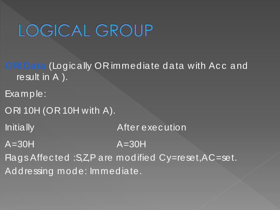
ORI Data (Logically OR immediate data with Acc and result in A ).
Example:
ORI 10H (OR 10H with A).
Initially After execution
A=30H A=30H Flags Affected :S,Z,P are modified Cy=reset,AC=set. Addressing mode: Immediate.
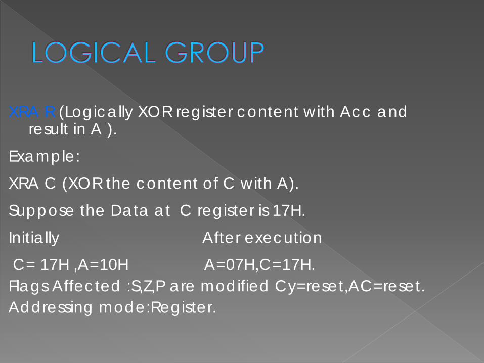
XRA R (Logically XOR register content with Acc and result in A ).
Example: XRA C (XOR the content of C with A). Suppose the Data at C register is 17H. Initially After execution C= 17H ,A=10H A=07H,C=17H. Flags Affected :S,Z,P are modified Cy=reset,AC=reset. Addressing mode:Register.
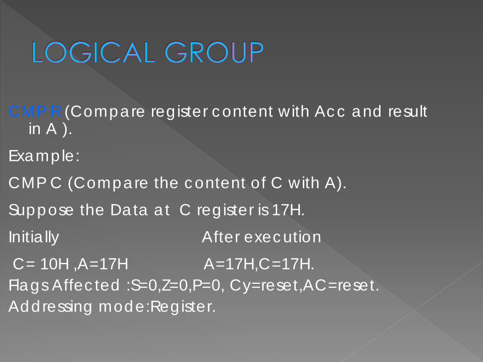
CMP R (Compare register content with Acc and result in A ).
Example: CMP C (Compare the content of C with A). Suppose the Data at C register is 17H. Initially After execution C= 10H ,A=17H A=17H,C=17H. Flags Affected :S=0,Z=0,P=0, Cy=reset,AC=reset. Addressing mode:Register.

CPI Data (Compare immediate data with Acc ).
Example:
CPI 10H (Compare the content of C with A).
Initially After execution
A=17H A=17H. Flags Affected :S=0,Z=0,P=0, Cy=reset,AC=reset. Addressing mode:Immediate.
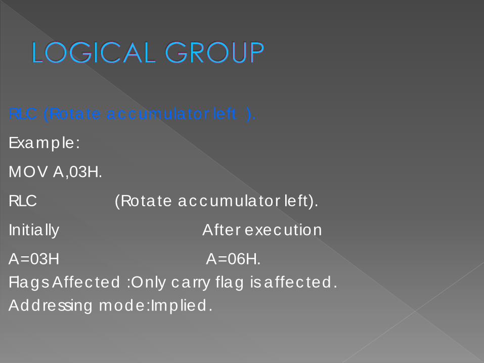
RLC (Rotate accumulator left ).
Example:
MOV A,03H.
RLC (Rotate accumulator left).
Initially After execution
A=03H A=06H. Flags Affected :Only carry flag is affected. Addressing mode:Implied.

RAL (Rotate accumulator left with carry ).
Example:
MOV A,03H.
RAL (Rotate accumulator left with carry).
Initially After execution
A=03H , carry =01H A=07H. Flags Affected :Only carry flag is affected. Addressing mode:Implied.

RRC (Rotate accumulator right ).
Example:
MOV A,03H.
RRC (Rotate accumulator right).
Initially After execution
A=03H , A=81H. Flags Affected :Only carry flag is affected. Addressing mode:Implied.
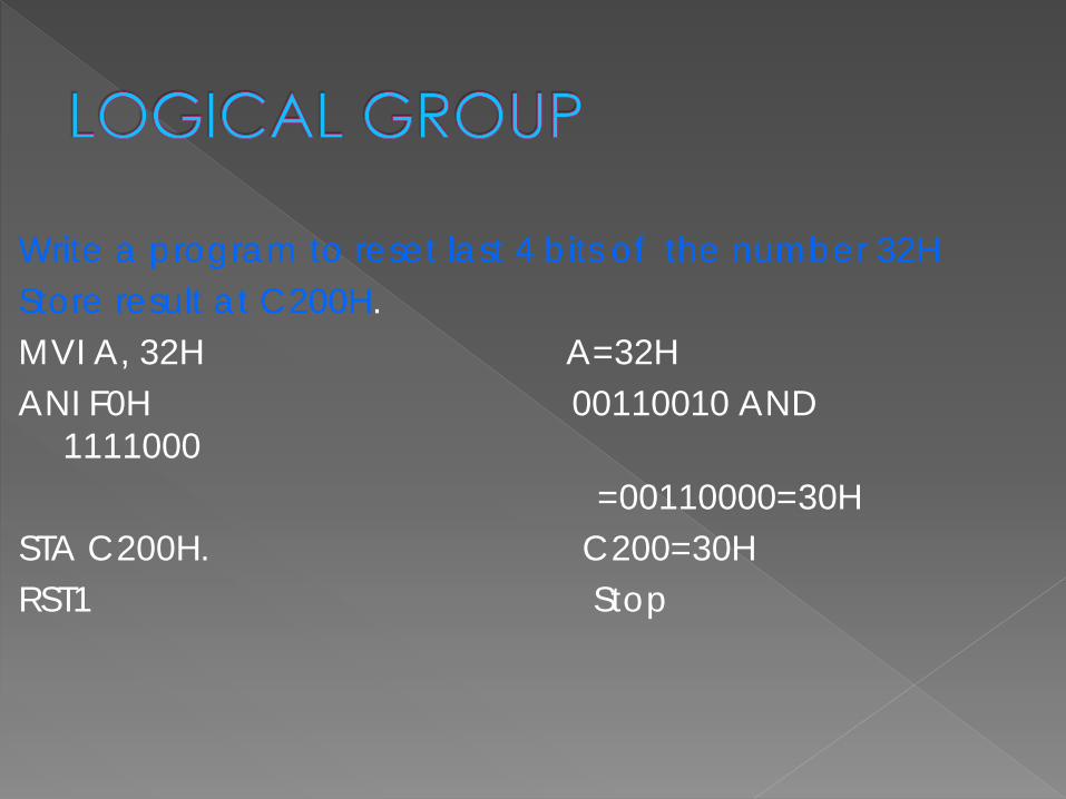
Write a program to reset last 4 bits of the number 32H Store result at C200H. MVI A, 32H A=32H ANI F0H 00110010 AND
1111000 =00110000=30H STA C200H. C200=30H RST1 Stop

JMP address(Unconditional jump to address) Example: JMP C200H. After this instruction the Program Counter is loaded
with this location and starts executing and the contents of PC are loaded on Stack.
Flags Affected :No Flags are affected. Addressing mode:Immediate.

Example: CALL C200H. After this instruction the Program Counter is loaded
with this location and starts executing and the contents of PC are loaded on Stack.
Flags Affected :No Flags are affected. Addressing mode:Immediate

Conditional Jump Instructions. JC (Jump if Carry flag is set) JNC (Jump if Carry flag is reset) JZ (Jump if zero flag set) JNZ (Jump if zero flag is reset) JPE (Jump if parity flag is set) JPO (Jump if parity odd or P flag is reset ) JP (Jump if sign flag reset ) JM (Jump if sign flag is set or minus)

Conditional Call Instructions. CC (Call if Carry flag is set) CNC (Call if Carry flag is reset) CZ (Call if zero flag set) CNZ (Call if zero flag is reset) CPE (Call if parity flag is set) CPO (Call if parity odd or P flag is reset ) CP (Call if sign flag reset ) CM (Call if sign flag is set or minus)
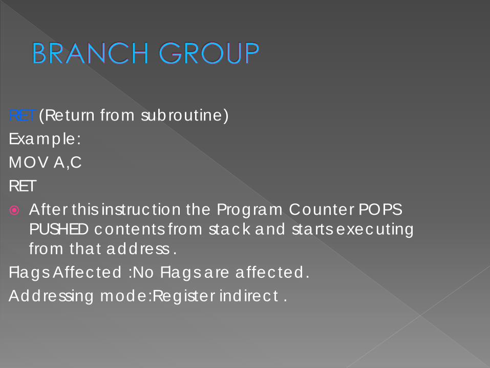
RET (Return from subroutine) Example: MOV A,C RET After this instruction the Program Counter POPS
PUSHED contents from stack and starts executing from that address .
Flags Affected :No Flags are affected. Addressing mode:Register indirect .

RST (Restart instruction) Example: MOV A,C RST 1. After this instruction the Program Counter goes to
address 0008H and starts executing from that address .
Flags Affected :No Flags are affected. Addressing mode:Register indirect.

The addresses of the respective RST commands are: Instruction Address RST 0 0000H RST 1 0008H RST 2 0010H RST 3 0018H RST 4 0020H RST 5 0028H RST 6 0030H RST 7 0038H
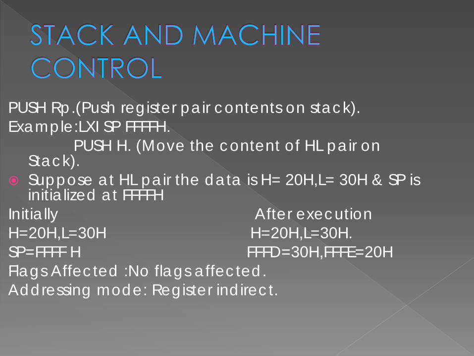
PUSH Rp.(Push register pair contents on stack). Example:LXI SP FFFFH. PUSH H. (Move the content of HL pair on
Stack). Suppose at HL pair the data is H= 20H,L= 30H & SP is
initialized at FFFFH Initially After execution H=20H,L=30H H=20H,L=30H. SP=FFFF H FFFD=30H,FFFE=20H Flags Affected :No flags affected. Addressing mode: Register indirect.
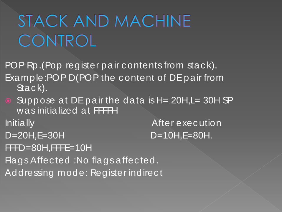
POP Rp.(Pop register pair contents from stack). Example:POP D(POP the content of DE pair from
Stack). Suppose at DE pair the data is H= 20H,L= 30H SP
was initialized at FFFFH Initially After execution D=20H,E=30H D=10H,E=80H. FFFD=80H,FFFE=10H Flags Affected :No flags affected. Addressing mode: Register indirect
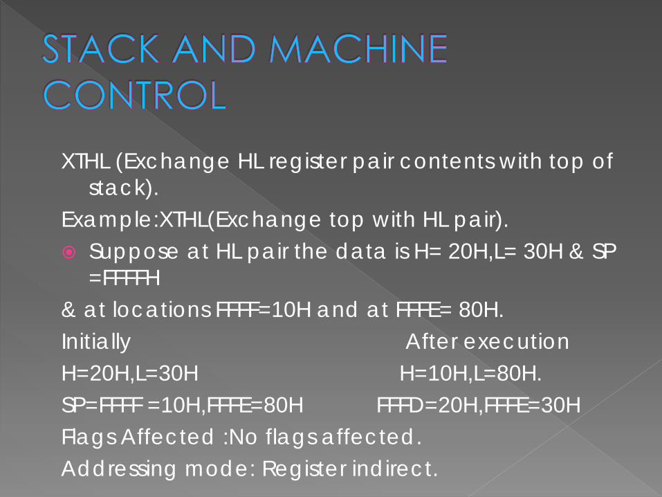
XTHL (Exchange HL register pair contents with top of stack).
Example:XTHL(Exchange top with HL pair). Suppose at HL pair the data is H= 20H,L= 30H & SP
=FFFFH & at locations FFFF=10H and at FFFE= 80H. Initially After execution H=20H,L=30H H=10H,L=80H. SP=FFFF =10H,FFFE=80H FFFD=20H,FFFE=30H Flags Affected :No flags affected. Addressing mode: Register indirect.
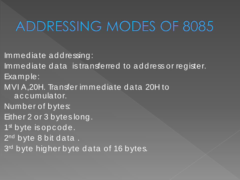
Immediate addressing: Immediate data is transferred to address or register. Example: MVI A,20H. Transfer immediate data 20H to
accumulator. Number of bytes: Either 2 or 3 bytes long. 1st byte is opcode. 2nd byte 8 bit data . 3rd byte higher byte data of 16 bytes.

Register addressing: Data is transferred from one register to other. Example: MOV A, C :Transfer data from C register to
accumulator. Number of bytes: Only 1 byte long. One byte is opcode.

Direct addressing: Data is transferred from direct address to other
register or vice-versa. Example: LDA C200H .Transfer contents from C200H to Acc. Number of bytes: These are 3 bytes long. 1st byte is opcode. 2nd byte lower address. 3rd byte higher address.
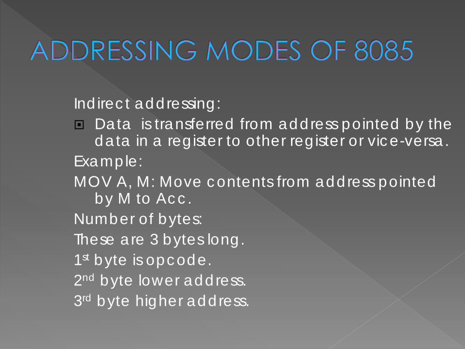
Indirect addressing: Data is transferred from address pointed by the
data in a register to other register or vice-versa. Example: MOV A, M: Move contents from address pointed
by M to Acc. Number of bytes: These are 3 bytes long. 1st byte is opcode. 2nd byte lower address. 3rd byte higher address.

Implied addressing: These doesn’t require any operand. The data is
specified in Opcode itself. Example: RAL: Rotate left with carry. No.of Bytes: These are single byte instruction or Opcode only.

Write a program to transfer a block of data from C550H to C55FH. Store the data from C570H to C57FH .
LXI H ,C550H LXI B ,C570H MVI D,0FH UP MOV A,M STAX B INX H INX B DCR D JNZ UP RST1
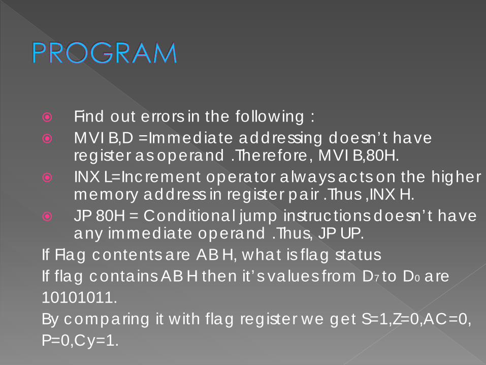
Find out errors in the following : MVI B,D =Immediate addressing doesn’t have
register as operand .Therefore, MVI B,80H. INX L=Increment operator always acts on the higher
memory address in register pair .Thus ,INX H. JP 80H = Conditional jump instructions doesn’t have
any immediate operand .Thus, JP UP. If Flag contents are AB H, what is flag status If flag contains AB H then it’s values from D7 to D0 are 10101011. By comparing it with flag register we get S=1,Z=0,AC=0, P=0,Cy=1.
11. What are the instructions for the following actions? Load the PC with second and third byte of instruction. LXI H, C200H PCHL Load PC with HL content Thus PC= L,PC +1=H. No change in normal execution except increment the
PC. NOP (No operation) This instruction has no effect on code only used to
cause delay .

Write a program to add 10 data bytes. Data is stored from locations C200. Store result at C300H.
LXI H,C200 H MVI C, 0A H UP MVI A,00 H MOV B,M ADD B INX H DCR C JNZ UP STA C300H RST1.
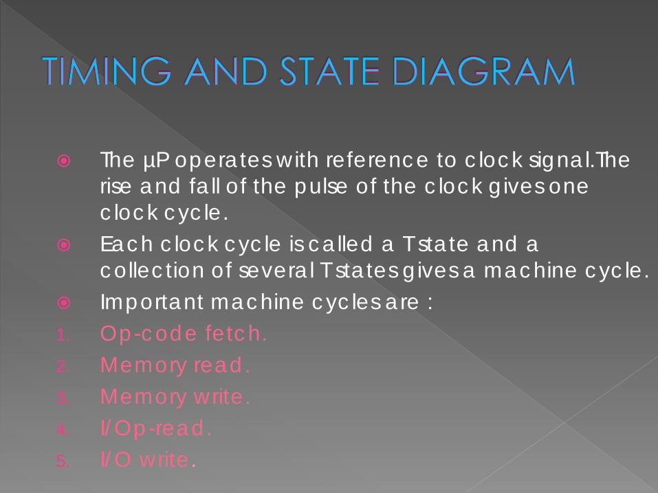
The µP operates with reference to clock signal.The rise and fall of the pulse of the clock gives one clock cycle.
Each clock cycle is called a T state and a collection of several T states gives a machine cycle.
Important machine cycles are : 1. Op-code fetch. 2. Memory read. 3. Memory write. 4. I/Op-read. 5. I/O write.

Op-code Fetch:It basically requires 4 T states from T1-T4
The ALE pin goes high at first T state always. AD0-AD7 are used to fetch OP-code and store the
lower byte of Program Counter. A8-A15 store the higher byte of the Program
Counter while IO/M¯ will be low since it is memory related operation.
RD¯ will only be low at the Op-code fetching time. WR¯ will be at HIGH level since no write operation
is done. S0=1,S1=1 for Op-code fetch cycle.
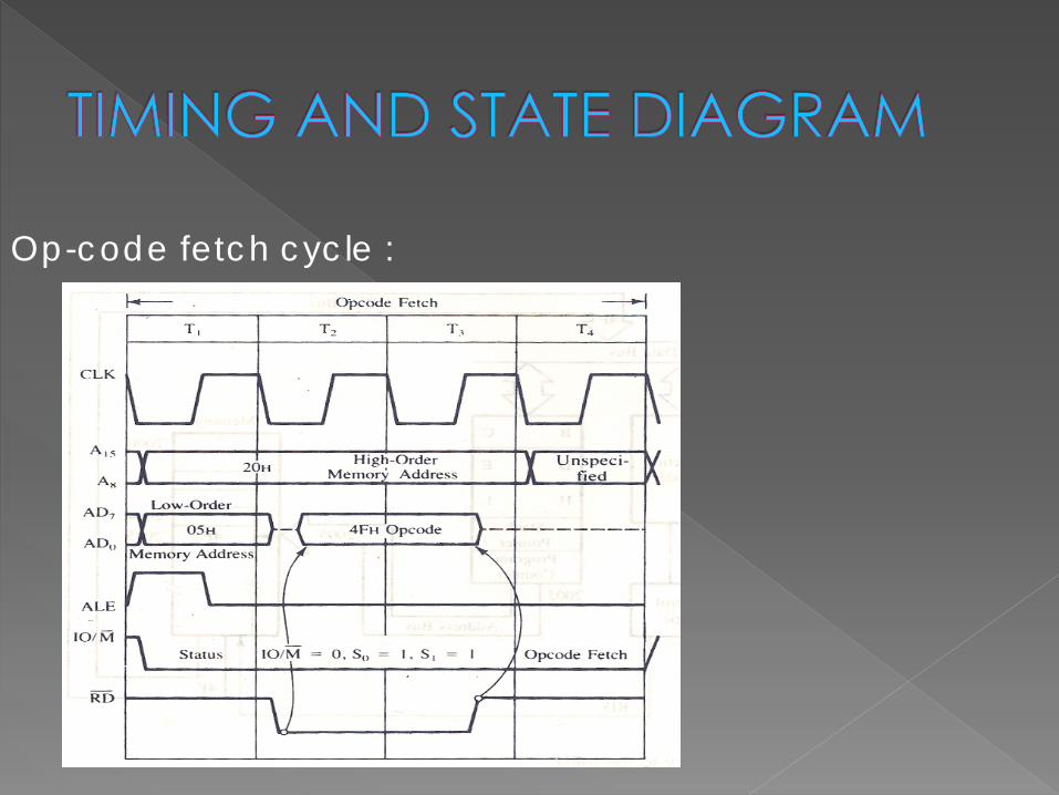
Op-code fetch cycle :

Memory Read Cycle: It basically requires 3T states from T1-T3 .
The ALE pin goes high at first T state always. AD0-AD7 are used to fetch data from memory and
store the lower byte of address. A8-A15 store the higher byte of the address while
IO/M¯ will be low since it is memory related operation.
RD¯ will only be low at the data fetching time. WR¯ will be at HIGH level since no write operation is
done. S0=0,S1=1 for Memory read cycle.

Memory write Cycle: It basically requires 3T states from T1-T3 .
The ALE pin goes high at first T state always. AD0-AD7 are used to fetch data from CPU and
store the lower byte of address. A8-A15 store the higher byte of the address while
IO/M¯ will be low since it is memory related operation.
RD¯ will be HIGH since no read operation is done. WR¯ will be at LOW level only when data fetching
is done. S0=1,S1=0 for Memory write cycle.

Calculation of Delay using 8 bit counter: Consider following example: MVI C, count(8 bit) H 7 T states
UP DCR C 4 T states JNZ UP 10/7 T RET 10T Here loop UP is executed (N-1) times. Thus delay is Td=M+[(count)x N) -3. Where M= no.of T states outside loop. N=no.of T states inside loop.

Here value of M= 17, N= 14. The maximum delay will occur if count is 255 or FF
H. Thus Td max =17+[255x14]-3= 3584 T states. For 0.5 µsec delay for a T state, we get Td max=0.5 µsec x 3584= 1792 µsec or 1.792 m sec.

• Generally µP 8085 can address 64 kB of memory .
• Generally EPROMS are used as program memory and RAM as data memory.
• We can interface Multiple RAMs and EPROMS to single µP .
• Memory interfacing includes 3 steps :
1. Select the chip.
2. Identify register.
3. Enable appropriate buffer.

Example: Interface 2Kbytes of Memory to 8085 with starting address 8000H.
Initially we realize that 2K memory requires 11 address lines
(2^11=2048). So we use A0-A10 . Write down A15 –A0
A15 14 13 12 11 10 9 8 7 6 5 4 3 2 1 0
1 1
0 0
0 0
0 0
0 0
0 1
0 1
0 1
0 1
0 1
0 1
0 1
0 1
0 1
0 1
0 1
ADD
8000H 87FFH
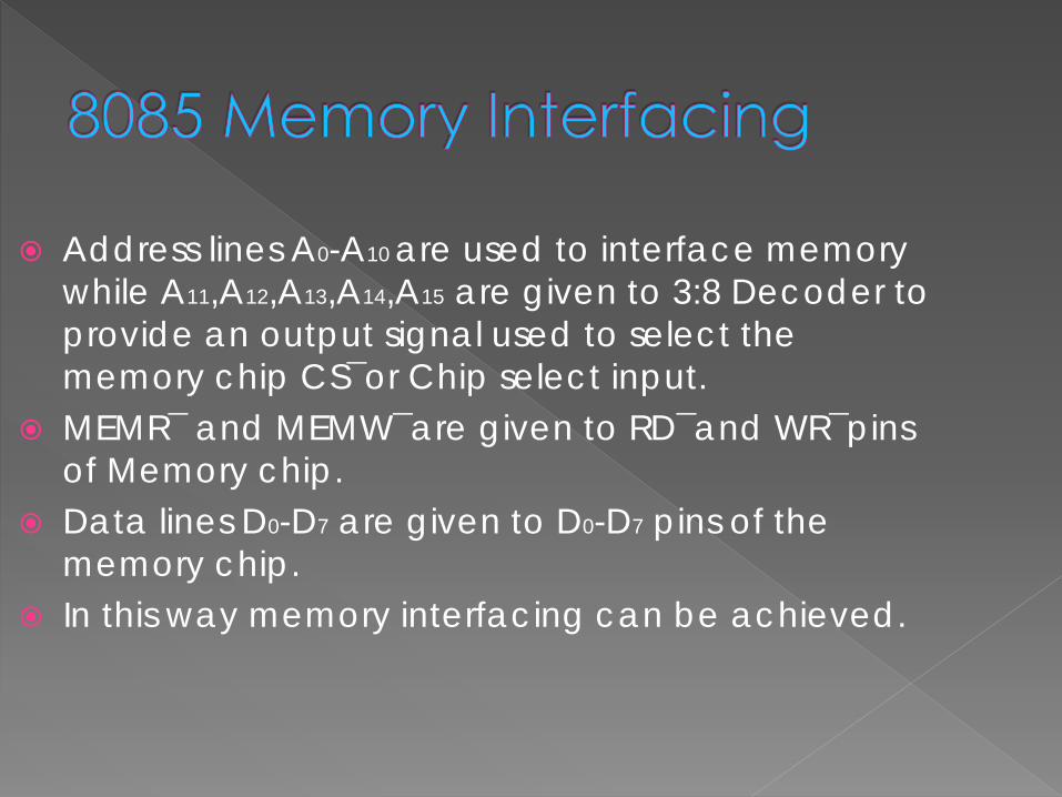
Address lines A0-A10 are used to interface memory while A11,A12,A13,A14,A15 are given to 3:8 Decoder to provide an output signal used to select the memory chip CS¯or Chip select input.
MEMR¯ and MEMW¯are given to RD¯and WR¯pins of Memory chip.
Data lines D0-D7 are given to D0-D7 pins of the memory chip.
In this way memory interfacing can be achieved.

The diagram of 2k interfacing is shown below:
A15-A8
Latch AD7-AD0
D7- D0
A7- A0
8085
ALE
IO/M RD WR
2K Byte Memory
Chip
WR RD
CS
A10- A0
A15- A11 3:8DECODER
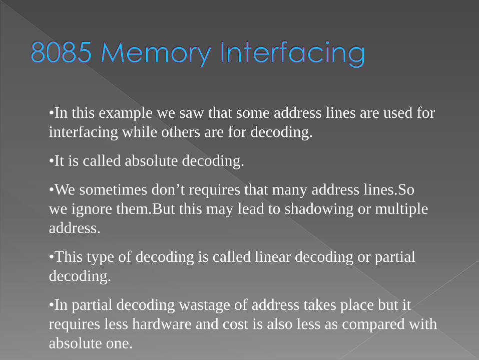
•In this example we saw that some address lines are used for interfacing while others are for decoding.
•It is called absolute decoding.
•We sometimes don’t requires that many address lines.So we ignore them.But this may lead to shadowing or multiple address.
•This type of decoding is called linear decoding or partial decoding.
•In partial decoding wastage of address takes place but it requires less hardware and cost is also less as compared with absolute one.

PA0-PA7 I/O Port A Pins PB0-PB7 I/O Port B Pins PC0-PC7 I/O Port C Pins D0-D7 I/O Data Pins RESET I Reset pin RD¯ I Read input WR ¯ I Write input A0-A1 I Address pins CS ¯ I Chip select Vcc , Gnd I +5volt supply


Data Bus Buffer: It is an 8 bit data buffer used to interface 8255 with 8085. It is connected to D0-D7 bits of 8255.
Read/write control logic:It consists of inputs RD¯,WR¯,A0,A1,CS¯ .
RD¯,WR¯ are used for reading and writing on to 8255 and are connected to MEMR¯,MEMW¯ of 8085 respectively.
A0,A1 are Port select signals used to select the particular port .
CS ¯ is used to select the 8255 device . It is controlled by the output of the 3:8 decoder used
to decode the address lines of 8085.
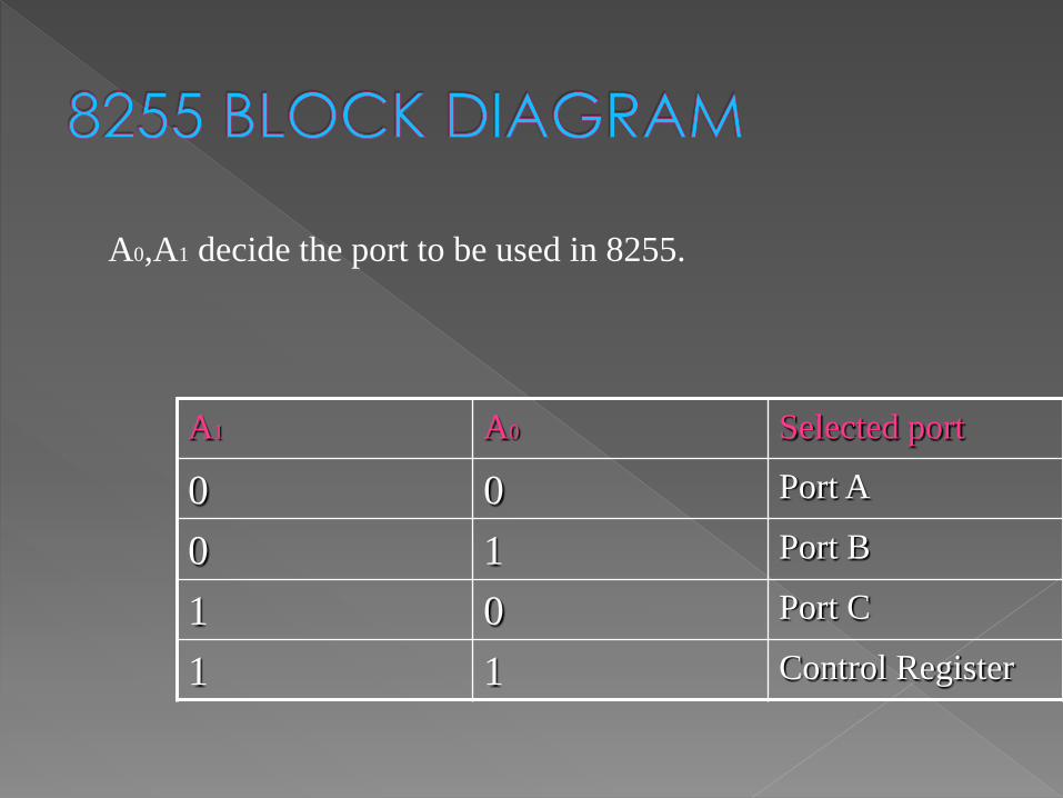
A1 A0 Selected port
0 0 Port A
0 1 Port B
1 0 Port C
1 1 Control Register
A0,A1 decide the port to be used in 8255.

Group A and Group B Control: Group A control consists of Port A and Port C
upper. Group B control consists of Port A and Port C lower. Each group is controlled through software. They receive commands from the RD¯, WR¯ pins to
allow access to bit pattern of 8085. The bit pattern consists of : 1. Information about which group is operated. 2. Information about mode of Operation.

PORT A,B:These are bi-directional 8 bit ports each and are used to interface 8255 with CPU or peripherals.
Port A is controlled by Group A while Port B is controlled by Group B Control.
PORT C: This is a bi-directional 8 bit port controlled partially by Group A control and partially by Group B control .
It is divided into two parts Port C upper and Port C lower each of a nibble.
It is used mainly for control signals and interfacing with peripherals.
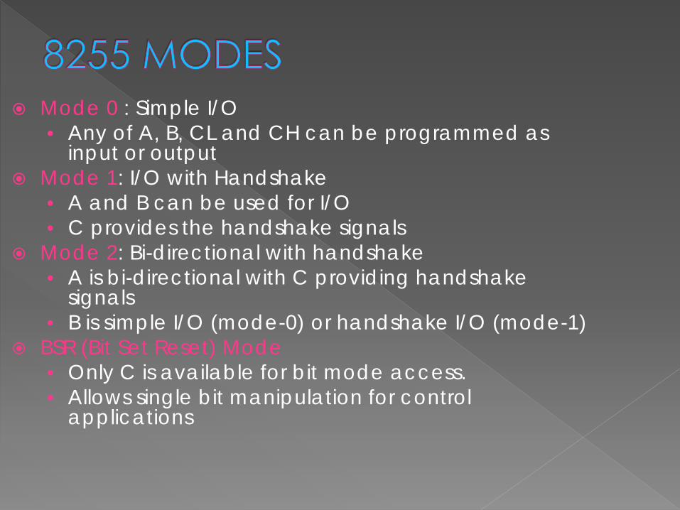
Mode 0 : Simple I/O • Any of A, B, CL and CH can be programmed as
input or output Mode 1: I/O with Handshake
• A and B can be used for I/O • C provides the handshake signals
Mode 2: Bi-directional with handshake • A is bi-directional with C providing handshake
signals • B is simple I/O (mode-0) or handshake I/O (mode-1)
BSR (Bit Set Reset) Mode • Only C is available for bit mode access. • Allows single bit manipulation for control
applications
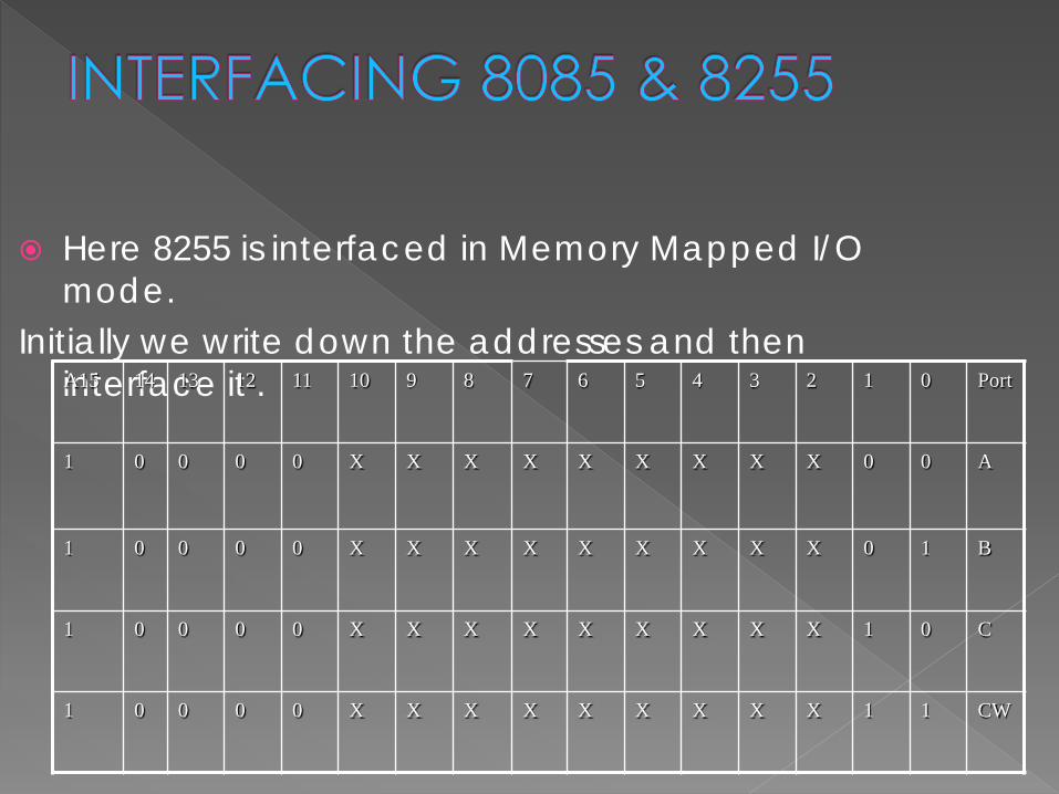
Here 8255 is interfaced in Memory Mapped I/O mode.
Initially we write down the addresses and then interface it . A15 14 13 12 11 10 9 8 7 6 5 4 3 2 1 0 Port
1 0 0 0 0 X X X X X X X X X 0 0 A
1 0 0 0 0 X X X X X X X X X 0 1 B
1 0 0 0 0 X X X X X X X X X 1 0 C
1 0 0 0 0 X X X X X X X X X 1 1 CW

Thus we get addresses ,considering don’t cares to be zero as
Port A =8000H Port B =8001H Port C =8002H CWR =8003H Then,we give A11,A12,A13 pins to A,B,C inputs of
Decoder to enable 8255 or Chip Select. A15 is logic 1 so it is given to active HIGH G1 pin& A14
,IO/M ¯ are given to active low G2B ¯,G2A ¯ pins. Output from Latch is given as A0,A1 pins to 8255 while
D0-D7 are given as data inputs.
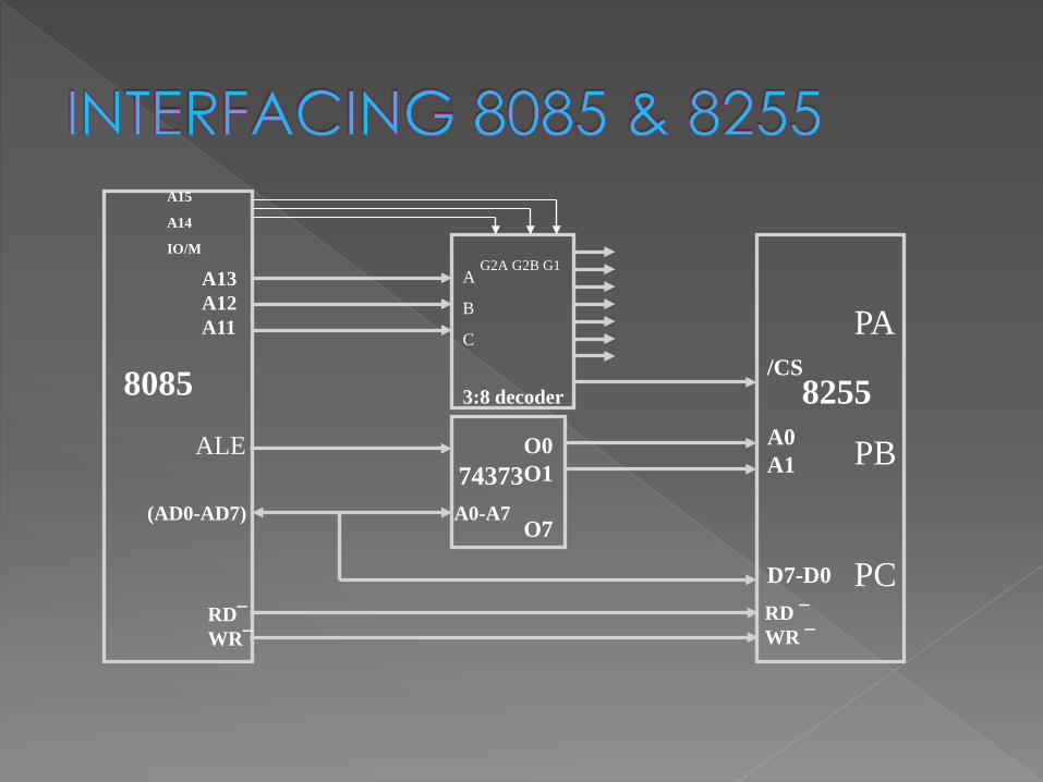
8255 8085 3:8 decoder
74373 (AD0-AD7)
D7-D0
A0-A7
/CS
A0 A1
O0 O1 O7
A13 A12 A11
ALE
RD ¯ WR ¯
RD¯ WR¯
G2A G2B G1
A15
A14
IO/M
A
B
C PA
PB
PC

Example:Take data from 8255 port B.Add FF H .Output result to port A.
MVI A,82H Initialize 8255. OUT 83H LDA 81H Take data from port B ADI FFH Add FF H to data OUT 80H. OUT Result to port A. RST1. STOP.


Serial Communications systems are of three types: Simplex: This is a one way communication. Only one party can speak. The other party only hears to the first one but cant
communicate. System A System B unidirectional
Transmitter
Receiver
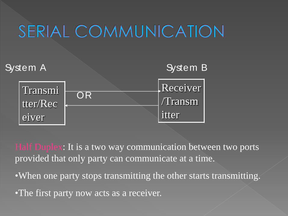
System A System B OR
Transmitter/Receiver
Receiver/Transmitter
Half Duplex: It is a two way communication between two ports provided that only party can communicate at a time.
•When one party stops transmitting the other starts transmitting.
•The first party now acts as a receiver.
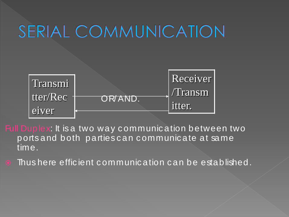
OR/AND. Full Duplex: It is a two way communication between two
ports and both parties can communicate at same time.
Thus here efficient communication can be established.
Transmitter/Receiver
Receiver/Transmitter.
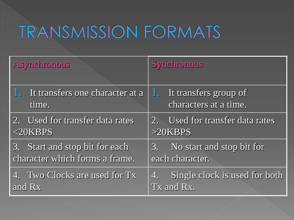
Asynchronous Synchronous
1. It transfers one character at a time.
1. It transfers group of characters at a time.
2. Used for transfer data rates <20KBPS
2. Used for transfer data rates >20KBPS
3. Start and stop bit for each character which forms a frame.
3. No start and stop bit for each character.
4. Two Clocks are used for Tx and Rx
4. Single clock is used for both Tx and Rx.

Interrupt is a process where an external device can get the attention of the microprocessor. The process starts from the I/O device The process is asynchronous.
Classification of Interrupts
Interrupts can be classified into two types: Maskable Interrupts (Can be delayed or
Rejected) Non-Maskable Interrupts (Can not be delayed
or Rejected)
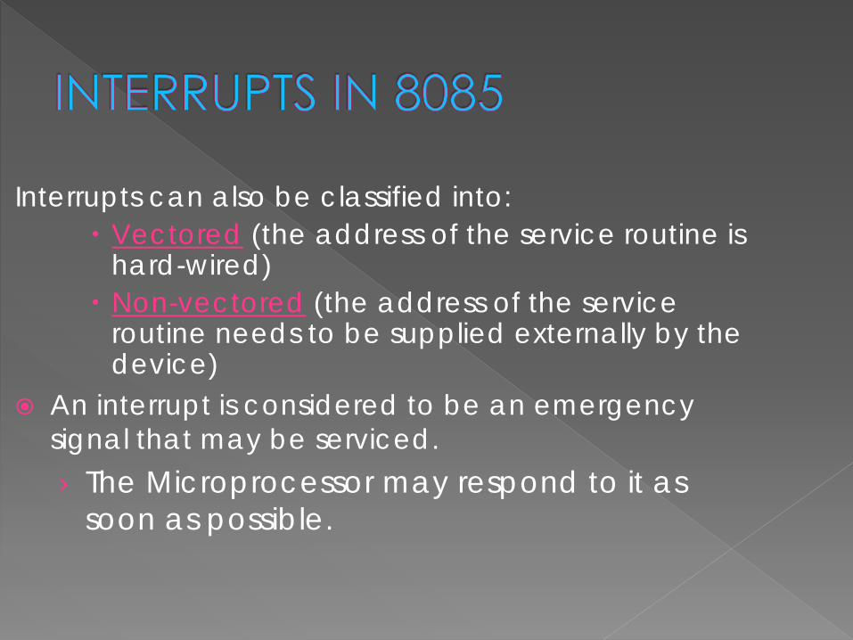
Interrupts can also be classified into: Vectored (the address of the service routine is
hard-wired) Non-vectored (the address of the service
routine needs to be supplied externally by the device)
An interrupt is considered to be an emergency signal that may be serviced. › The Microprocessor may respond to it as
soon as possible.

The 8085 has 5 interrupt inputs. The INTR input.
The INTR input is the only non-vectored interrupt. INTR is mask-able using the EI/DI instruction pair.
RST 5.5, RST 6.5, RST 7.5 are all automatically
vectored. RST 5.5, RST 6.5, and RST 7.5 are all mask-able.
TRAP is the only non-mask-able interrupt in the
8085 TRAP is also automatically vectored.

Non vectored interrupts: The 8085 recognizes 8 RESTART instructions: RST0 -
RST7 . Each of these would send the execution to a predetermined hard-wired memory location:
Restart Instruction
Equivalent to
RST0 CALL 0000H
RST1 CALL 0008H
RST2 CALL 0010H
RST3 CALL 0018H
RST4 CALL 0020H
RST5 CALL 0028H
RST6 CALL 0030H
RST7 CALL 0038H
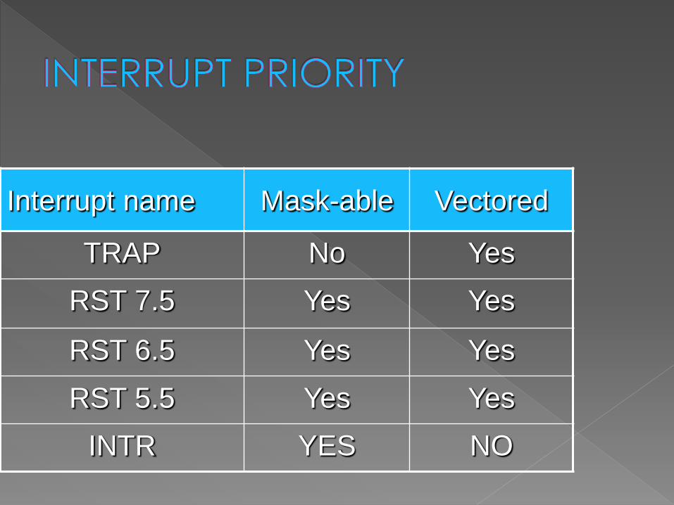
Interrupt name Mask-able Vectored
TRAP No Yes RST 7.5 Yes Yes
RST 6.5 Yes Yes RST 5.5 Yes Yes
INTR YES NO

101
SO
D
SD
E
XX
X
R7.
5 M
SE
M
7.5
M6.
5 M
5.5
0 1 2 3 4 5 6 7
RST5.5 Mask RST6.5 Mask RST7.5 Mask
} 0 - Available 1 - Masked
Mask Set Enable 0 - Ignore bits 0-2 1 - Set the masks according to bits 0-2
Force RST7.5 Flip Flop to reset Not Used
Enable Serial Data 0 - Ignore bit 7 1 - Send bit 7 to SOD pin
Serial Out Data
•SIM Instruction helps activate a particular interrupt.
•It can also mask a maskable interrupt.
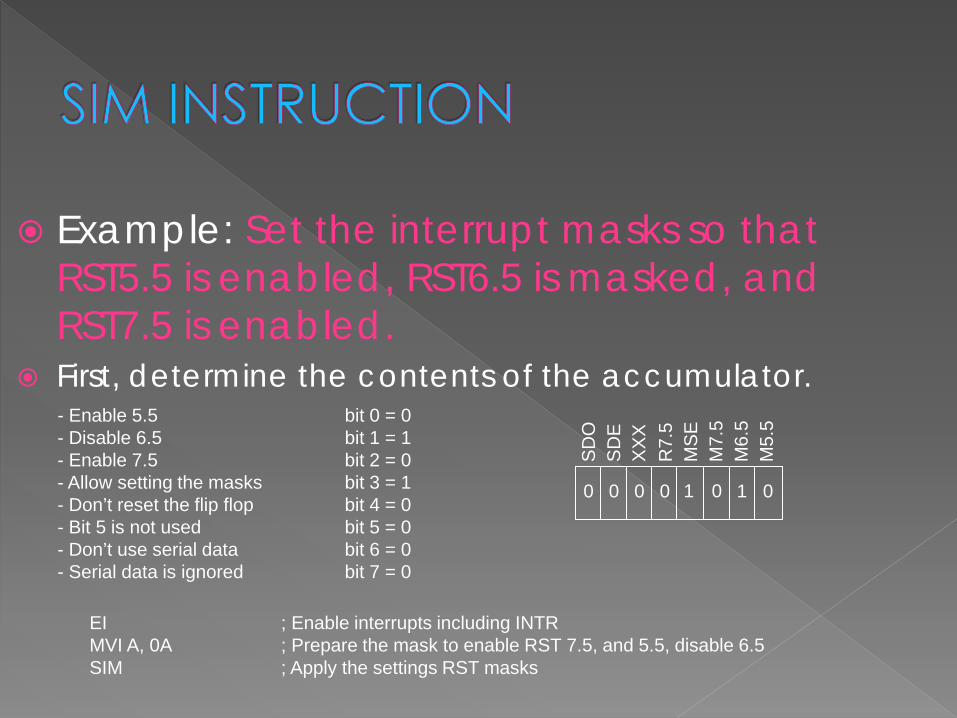
Example: Set the interrupt masks so that RST5.5 is enabled, RST6.5 is masked, and RST7.5 is enabled.
First, determine the contents of the accumulator. - Enable 5.5 bit 0 = 0
- Disable 6.5 bit 1 = 1 - Enable 7.5 bit 2 = 0 - Allow setting the masks bit 3 = 1 - Don’t reset the flip flop bit 4 = 0 - Bit 5 is not used bit 5 = 0 - Don’t use serial data bit 6 = 0 - Serial data is ignored bit 7 = 0
SD
O
SD
E
XX
X
R7.
5 M
SE
M
7.5
M6.
5 M
5.5
0 1 0 0 0 0 0 1
EI ; Enable interrupts including INTR MVI A, 0A ; Prepare the mask to enable RST 7.5, and 5.5, disable 6.5 SIM ; Apply the settings RST masks

Serial Data In
RST5.5 Interrupt Pending RST6.5 Interrupt Pending RST7.5 Interrupt Pending
0 - Available 1 - Masked
Interrupt Enable Value of the Interrupt Enable Flip Flop
SD
I P
7.5
P6.
5 P
5.5
IE
M7.
5 M
6.5
M5.
5
0 1 2 3 4 5 6 7
RST5.5 Mask RST6.5 Mask RST7.5 Mask
}
•Since the 8085 has five interrupt lines, interrupts may occur during an ISR and remain pending. •Using the RIM instruction, it is possible to can read the status of the interrupt lines and find if there are any pending interrupts.


Three independent 16 bit counters. 24 pin Dual in line Package. Counting facility in Both BCD and Binary modes. Dc to 2 MHz operating Frequency. Can be used as a clock generator.

SC1 SC0 RL1 RL0 M2 M1 M0 BCD D0 D7
0 0 Counter0
0 1 Counter1
1 0 Counter2
1 1 ILLEGAL
SC1 SC0 Select counter
0 0 Counter latching
0 1 Read/load LSB
1 0 Read/load MSB
1 1 R/L MSB 1st then LSB.
RL1 RL0 Read/Load

0 0 0 Mode 0
0 0 1 Mode 1 X 1 0 Mode 2 X 1 1 Mode 3 1 0 0 Mode 4 1 0 1 Mode 5
M2 M1 M0 BCD =0 Binary counter
BCD =1 BCD counter

Example: Use 8253 as a square wave generator with 1ms period if the input frequency is 1MHz.
We use counter 0 as a square wave generator and address of counter 0 =10H and control register =13H.
I/P frequency is 1MHz.So time is 1µsec. Count value = Required period /Input period =
1ms/1 µsec =1000(Decimal). Thus we use 8253 as a decimal counter.
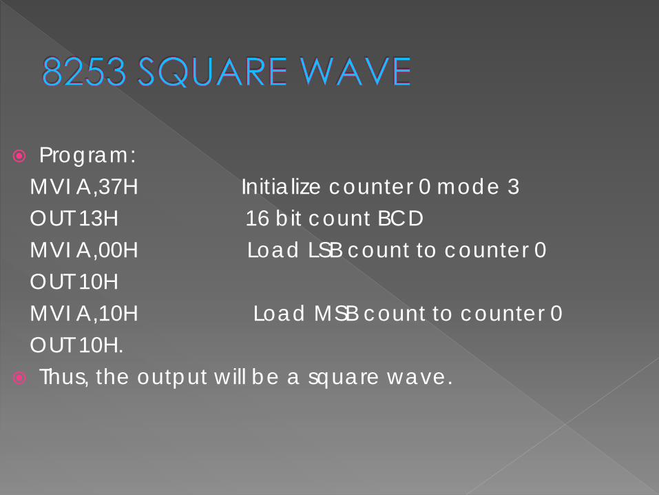
Program: MVI A,37H Initialize counter 0 mode 3 OUT 13H 16 bit count BCD MVI A,00H Load LSB count to counter 0 OUT 10H MVI A,10H Load MSB count to counter 0 OUT 10H. Thus, the output will be a square wave.
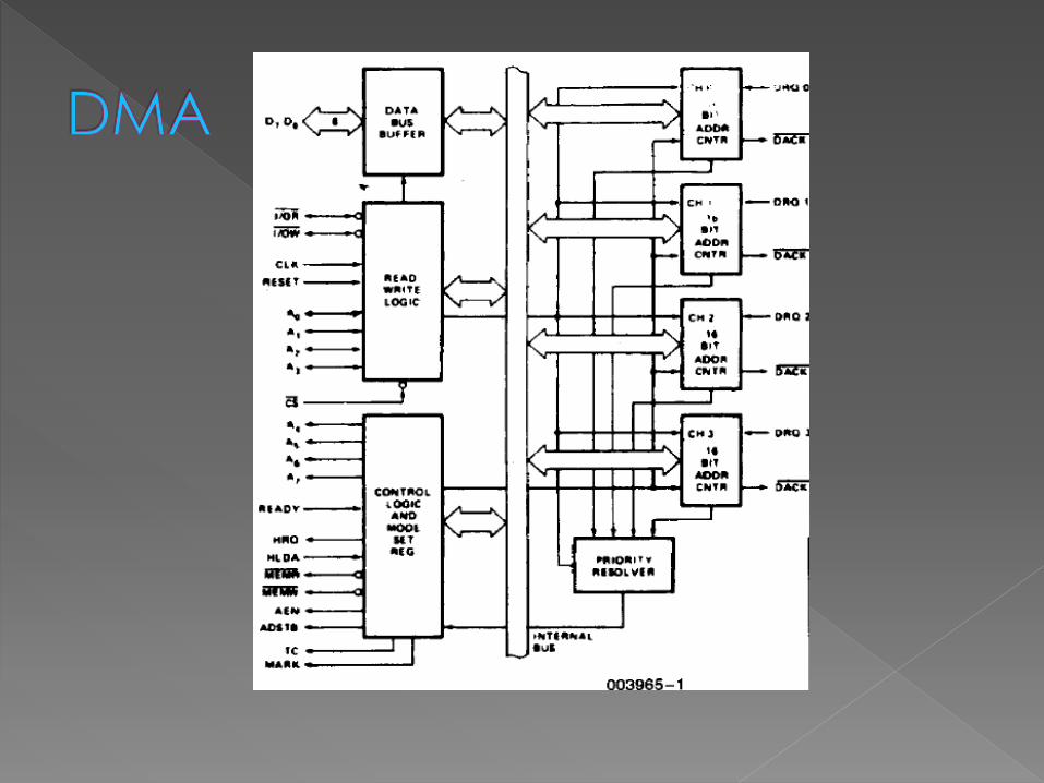

It is a 4 Channel DMA containing 4 individual I/P ,O/P Channels.
CH0,CH1,CH2,CH3
It is compatible with Intel processors. The maximum frequency is 3 MHz. It executes 3 cycles: 1. DMA read 2. DMA write. 3. DMA verify. The external device can terminate DMA Operation
1. Rotating priority mode:Each channel has equal priority.
Priority is shifted from one channel to other. 1. Fixed priority mode: Each channel has a fixed priority and if higher priority channels are busy then smaller priority
will get to serve. 1. Extended write mode: This mode is used to interface
slower devices to the system. 2. TC stop mode:If this bit is set the channel whose
terminal count is reached is disabled. 3. Auto reload mode: If this bit is set data is transferred
by channel 2 only.All other channels are not used.