8-Channel, 24-Bit, Simultaneous Sampling ADC with Power ...
22
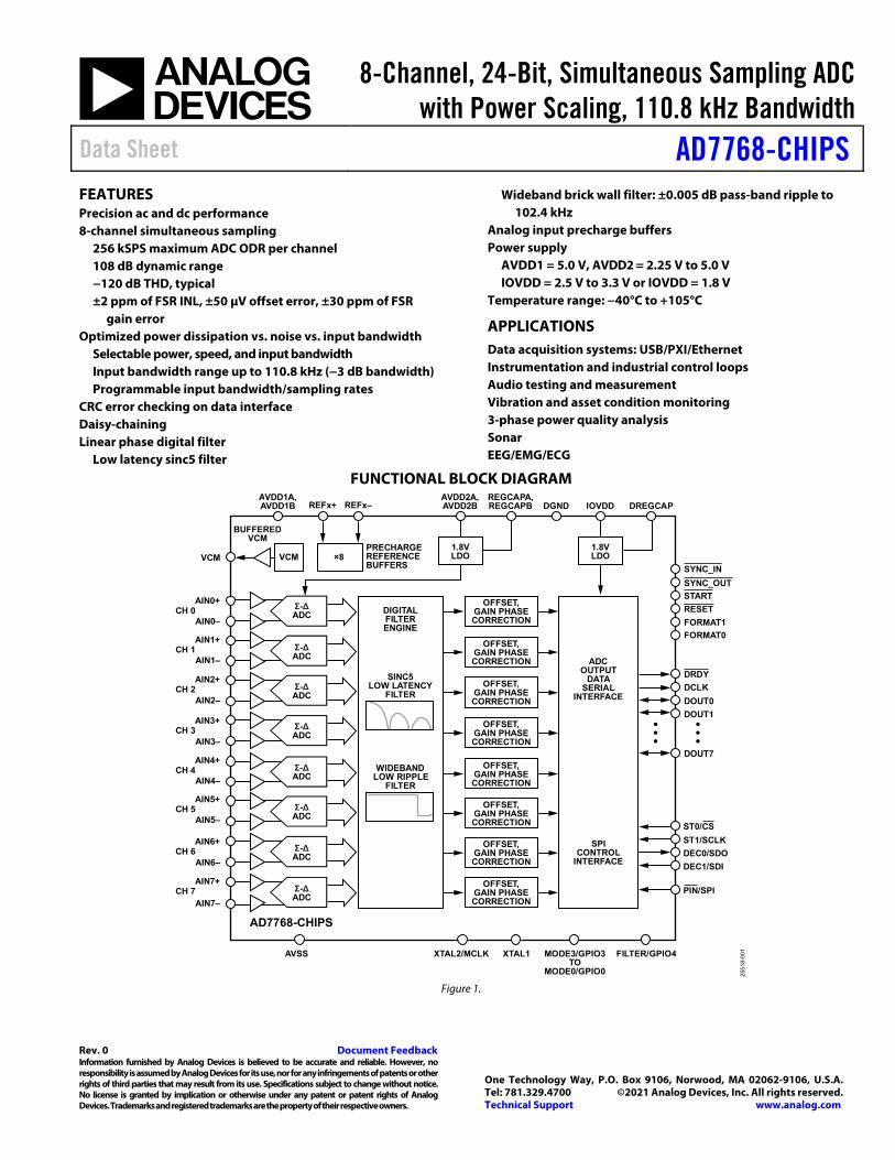
8-Channel, 24-Bit, Simultaneous Sampling ADC with Power Scaling, 110.8 kHz Bandwidth Data Sheet AD7768-CHIPS Rev. 0 Document Feedback Information furnished by Analog Devices is believed to be accurate and reliable. However, no responsibility is assumed by Analog Devices for its use, nor for any infringements of patents or other rights of third parties that may result from its use. Specifications subject to change without notice. No license is granted by implication or otherwise under any patent or patent rights of Analog Devices. Trademarks and registered trademarks are the property of their respective owners. One Technology Way, P.O. Box 9106, Norwood, MA 02062-9106, U.S.A. Tel: 781.329.4700 ©2021 Analog Devices, Inc. All rights reserved. Technical Support www.analog.com FEATURES Precision ac and dc performance 8-channel simultaneous sampling 256 kSPS maximum ADC ODR per channel 108 dB dynamic range −120 dB THD, typical ±2 ppm of FSR INL, ±50 μV offset error, ±30 ppm of FSR gain error Optimized power dissipation vs. noise vs. input bandwidth Selectable power, speed, and input bandwidth Input bandwidth range up to 110.8 kHz (−3 dB bandwidth) Programmable input bandwidth/sampling rates CRC error checking on data interface Daisy-chaining Linear phase digital filter Low latency sinc5 filter Wideband brick wall filter: ±0.005 dB pass-band ripple to 102.4 kHz Analog input precharge buffers Power supply AVDD1 = 5.0 V, AVDD2 = 2.25 V to 5.0 V IOVDD = 2.5 V to 3.3 V or IOVDD = 1.8 V Temperature range: −40°C to +105°C APPLICATIONS Data acquisition systems: USB/PXI/Ethernet Instrumentation and industrial control loops Audio testing and measurement Vibration and asset condition monitoring 3-phase power quality analysis Sonar EEG/EMG/ECG FUNCTIONAL BLOCK DIAGRAM ADC OUTPUT DATA SERIAL INTERFACE DIGITAL FILTER ENGINE WIDEBAND LOW RIPPLE FILTER SINC5 LOW LATENCY FILTER SPI CONTROL INTERFACE 1.8V LDO SYNC_IN 1.8V LDO BUFFERED VCM VCM AIN1+ CH 1 AIN1– AIN2+ CH 2 AIN2– AIN3+ CH 3 AIN3– AIN4+ CH 4 AIN4– AIN5+ CH 5 AIN5– AIN6+ CH 6 AIN6– AIN7+ CH 7 AIN7– AIN0+ CH 0 AIN0– VCM ×8 PRECHARGE REFERENCE BUFFERS SYNC_OUT START RESET FORMAT1 FORMAT0 DRDY DCLK DOUT0 DOUT1 ST0/CS PIN/SPI ST1/SCLK DEC0/SDO DEC1/SDI DOUT7 AVSS XTAL2/MCLK XTAL1 MODE3/GPIO3 TO MODE0/GPIO0 FILTER/GPIO4 Σ-Δ ADC Σ-Δ ADC Σ-Δ ADC Σ-Δ ADC Σ-Δ ADC Σ-Δ ADC Σ-Δ ADC Σ-Δ ADC DGND AD7768-CHIPS IOVDD DREGCAP REGCAPA, REGCAPB AVDD2A, AVDD2B AVDD1A, AVDD1B REFx+ REFx– OFFSET, GAIN PHASE CORRECTION OFFSET, GAIN PHASE CORRECTION OFFSET, GAIN PHASE CORRECTION OFFSET, GAIN PHASE CORRECTION OFFSET, GAIN PHASE CORRECTION OFFSET, GAIN PHASE CORRECTION OFFSET, GAIN PHASE CORRECTION OFFSET, GAIN PHASE CORRECTION 25518-001 Figure 1.
Transcript of 8-Channel, 24-Bit, Simultaneous Sampling ADC with Power ...
8-Channel, 24-Bit, Simultaneous Sampling ADCwith Power Scaling, 110.8 kHz Bandwidth
Data Sheet AD7768-CHIPS
Rev. 0 Document Feedback Information furnished by Analog Devices is believed to be accurate and reliable. However, no responsibility is assumed by Analog Devices for its use, nor for any infringements of patents or other rights of third parties that may result from its use. Specifications subject to change without notice. No license is granted by implication or otherwise under any patent or patent rights of Analog Devices. Trademarks and registered trademarks are the property of their respective owners.
One Technology Way, P.O. Box 9106, Norwood, MA 02062-9106, U.S.A.Tel: 781.329.4700 ©2021 Analog Devices, Inc. All rights reserved. Technical Support www.analog.com
FEATURES Precision ac and dc performance 8-channel simultaneous sampling
256 kSPS maximum ADC ODR per channel 108 dB dynamic range −120 dB THD, typical ±2 ppm of FSR INL, ±50 μV offset error, ±30 ppm of FSR
gain error Optimized power dissipation vs. noise vs. input bandwidth
Selectable power, speed, and input bandwidth Input bandwidth range up to 110.8 kHz (−3 dB bandwidth) Programmable input bandwidth/sampling rates
CRC error checking on data interface Daisy-chaining Linear phase digital filter
Low latency sinc5 filter
Wideband brick wall filter: ±0.005 dB pass-band ripple to 102.4 kHz
Analog input precharge buffers Power supply
AVDD1 = 5.0 V, AVDD2 = 2.25 V to 5.0 V IOVDD = 2.5 V to 3.3 V or IOVDD = 1.8 V
Temperature range: −40°C to +105°C
APPLICATIONS Data acquisition systems: USB/PXI/Ethernet Instrumentation and industrial control loops Audio testing and measurement Vibration and asset condition monitoring 3-phase power quality analysis Sonar EEG/EMG/ECG
FUNCTIONAL BLOCK DIAGRAM
ADCOUTPUT
DATASERIAL
INTERFACE
DIGITALFILTERENGINE
WIDEBANDLOW RIPPLE
FILTER
SINC5LOW LATENCY
FILTER
SPICONTROL
INTERFACE
1.8VLDO
SYNC_IN
1.8VLDO
BUFFEREDVCM
VCM
AIN1+CH 1
AIN1–
AIN2+CH 2
AIN2–
AIN3+CH 3
AIN3–
AIN4+CH 4
AIN4–
AIN5+CH 5
AIN5–
AIN6+CH 6
AIN6–
AIN7+CH 7
AIN7–
AIN0+CH 0
AIN0–
VCM ×8PRECHARGEREFERENCEBUFFERS
SYNC_OUT
START
RESET
FORMAT1
FORMAT0
DRDY
DCLK
DOUT0
DOUT1
ST0/CS
PIN/SPI
ST1/SCLK
DEC0/SDO
DEC1/SDI
DOUT7
AVSS XTAL2/MCLK XTAL1 MODE3/GPIO3TO
MODE0/GPIO0
FILTER/GPIO4
Σ-ΔADC
Σ-ΔADC
Σ-ΔADC
Σ-ΔADC
Σ-ΔADC
Σ-ΔADC
Σ-ΔADC
Σ-ΔADC
DGND
AD7768-CHIPS
IOVDD DREGCAPREGCAPA,REGCAPB
AVDD2A,AVDD2B
AVDD1A,AVDD1B REFx+ REFx–
OFFSET,GAIN PHASECORRECTION
OFFSET,GAIN PHASECORRECTION
OFFSET,GAIN PHASECORRECTION
OFFSET,GAIN PHASECORRECTION
OFFSET,GAIN PHASECORRECTION
OFFSET,GAIN PHASECORRECTION
OFFSET,GAIN PHASECORRECTION
OFFSET,GAIN PHASECORRECTION
25518-001
Figure 1.
AD7768-CHIPS Data Sheet
Rev. 0 | Page 2 of 22
TABLE OF CONTENTS Features .............................................................................................. 1 Applications ...................................................................................... 1 Functional Block Diagram .............................................................. 1 Revision History ............................................................................... 2 General Description ......................................................................... 3 Specifications .................................................................................... 4
1.8 V IOVDD Specifications ....................................................... 9 Timing Specifications ................................................................ 12
1.8 V IOVDD Timing Specifications ...................................... 13 Absolute Maximum Ratings ......................................................... 17
ESD Caution ............................................................................... 17 Pin Configuration and Function Descriptions .......................... 18 Outline Dimensions ....................................................................... 21
Die Specifications and Assembly Recommendations ........... 21 Ordering Guide .......................................................................... 22
REVISION HISTORY 3/2021—Revision 0: Initial Version
Data Sheet AD7768-CHIPS
Rev. 0 | Page 3 of 22
GENERAL DESCRIPTION The AD7768-CHIPS is an 8-channel simultaneous sampling sigma-delta (Σ-Δ) analog-to-digital converter (ADC) with a Σ-Δ modulator and digital filter per channel, enabling synchronized sampling of ac and dc signals.
The AD7768-CHIPS achieves 108 dB dynamic range at a maximum input bandwidth of 110.8 kHz, combined with a typical performance of ±2 ppm integral nonlinearity (INL), ±50 μV offset error, and ±30 ppm of full-scale range (FSR) gain error.
The AD7768-CHIPS user can trade off input bandwidth, output data rate (ODR), and power dissipation, and select one of three power modes to optimize for noise targets and power consumption. The flexibility of the AD7768-CHIPS allows the device to become a reusable platform for low power dc and high performance ac measurement modules.
The AD7768-CHIPS has three modes: fast mode (256 kSPS maximum, 110.8 kHz input bandwidth), median mode (128 kSPS maximum, 55.4 kHz input bandwidth) and low power mode (32 kSPS maximum, 13.8 kHz input bandwidth).
The AD7768-CHIPS offers extensive digital filtering capabilities, such as a wideband, a low ±0.005 dB pass-band ripple, an antialiasing low-pass filter with sharp roll-off, and 105 dB stop band attenuation at the Nyquist frequency.
Frequency domain measurements can use the wideband linear phase filter. This filter has a flat pass band (±0.005 dB ripple) from dc to 102.4 kHz at 256 kSPS, from dc to 51.2 kHz at 128 kSPS, or from dc to 12.8 kHz at 32 kSPS.
The AD7768-CHIPS also offers sinc response via a sinc5 filter, a low latency path for low bandwidth, and low noise measurements. The wideband and sinc5 filters can be selected and run on a per channel basis.
Within these filter options, the user can improve the dynamic range by selecting from decimation rates of ×32, ×64, ×128, ×256, ×512, and ×1024. The ability to vary the decimation filtering optimizes noise performance to the required input bandwidth.
Embedded analog functionality on each ADC channel makes design easier, such as a precharge buffer on each analog input that reduces analog input current and a precharge reference buffer per channel that reduces input current and glitches on the reference input terminals.
The device operates with a 5 V AVDD1A and AVDD1B supply, a 2.25 V to 5.0 V AVDD2A and AVDD2B supply, and a 2.5 V to 3.3 V or 1.8 V IOVDD supply.
The device requires an external reference. The absolute input reference voltage range is 1 V to AVDD1 − AVSS.
For the purposes of clarity in this data sheet, the AVDD1A and AVDD1B supplies are referred to as AVDD1, and the AVDD2A and AVDD2B supplies are referred to as AVDD2. For the negative supplies, AVSS refers to the AVSS1A, AVSS1B, AVSS2A, AVSS2B, and AVSS pins.
The specified operating temperature range is −40°C to +105°C.
Throughout this data sheet, multifunction pins, such as XTAL2/MCLK, are referred to either by the entire pin name or by a single function of the pin, for example MCLK, when only that function is relevant.
Additional application and technical information can be found in the AD7768 data sheet.
AD7768-CHIPS Data Sheet
Rev. 0 | Page 4 of 22
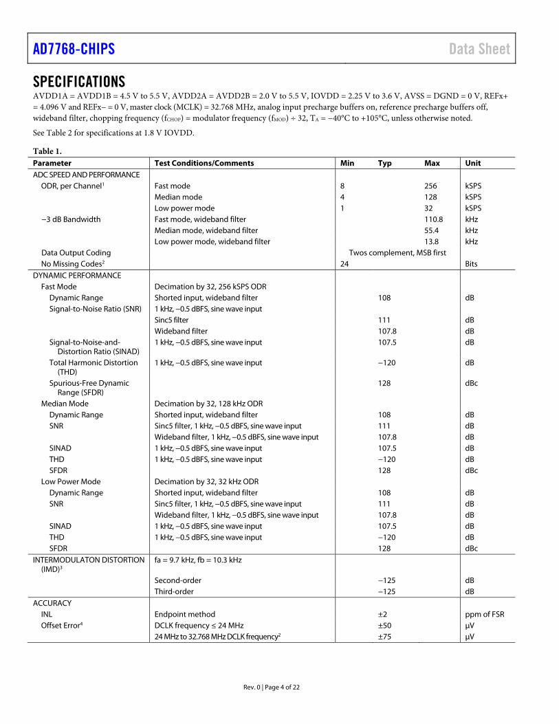
SPECIFICATIONS AVDD1A = AVDD1B = 4.5 V to 5.5 V, AVDD2A = AVDD2B = 2.0 V to 5.5 V, IOVDD = 2.25 V to 3.6 V, AVSS = DGND = 0 V, REFx+ = 4.096 V and REFx− = 0 V, master clock (MCLK) = 32.768 MHz, analog input precharge buffers on, reference precharge buffers off, wideband filter, chopping frequency (fCHOP) = modulator frequency (fMOD) ÷ 32, TA = −40°C to +105°C, unless otherwise noted.
See Table 2 for specifications at 1.8 V IOVDD.
Table 1. Parameter Test Conditions/Comments Min Typ Max Unit ADC SPEED AND PERFORMANCE
ODR, per Channel1 Fast mode 8 256 kSPS Median mode 4 128 kSPS Low power mode 1 32 kSPS
−3 dB Bandwidth Fast mode, wideband filter 110.8 kHz Median mode, wideband filter 55.4 kHz Low power mode, wideband filter 13.8 kHz Data Output Coding Twos complement, MSB first No Missing Codes2 24 Bits
DYNAMIC PERFORMANCE Fast Mode Decimation by 32, 256 kSPS ODR
Dynamic Range Shorted input, wideband filter 108 dB Signal-to-Noise Ratio (SNR) 1 kHz, −0.5 dBFS, sine wave input Sinc5 filter 111 dB Wideband filter 107.8 dB Signal-to-Noise-and-
Distortion Ratio (SINAD) 1 kHz, −0.5 dBFS, sine wave input 107.5 dB
Total Harmonic Distortion (THD)
1 kHz, −0.5 dBFS, sine wave input −120 dB
Spurious-Free Dynamic Range (SFDR)
128 dBc
Median Mode Decimation by 32, 128 kHz ODR Dynamic Range Shorted input, wideband filter 108 dB SNR Sinc5 filter, 1 kHz, −0.5 dBFS, sine wave input 111 dB Wideband filter, 1 kHz, −0.5 dBFS, sine wave input 107.8 dB SINAD 1 kHz, −0.5 dBFS, sine wave input 107.5 dB THD 1 kHz, −0.5 dBFS, sine wave input −120 dB SFDR 128 dBc
Low Power Mode Decimation by 32, 32 kHz ODR Dynamic Range Shorted input, wideband filter 108 dB SNR Sinc5 filter, 1 kHz, −0.5 dBFS, sine wave input 111 dB Wideband filter, 1 kHz, −0.5 dBFS, sine wave input 107.8 dB SINAD 1 kHz, −0.5 dBFS, sine wave input 107.5 dB THD 1 kHz, −0.5 dBFS, sine wave input −120 dB SFDR 128 dBc
INTERMODULATON DISTORTION (IMD)3
fa = 9.7 kHz, fb = 10.3 kHz
Second-order −125 dB Third-order −125 dB
ACCURACY INL Endpoint method ±2 ppm of FSR Offset Error4 DCLK frequency ≤ 24 MHz ±50 μV 24 MHz to 32.768 MHz DCLK frequency2 ±75 μV
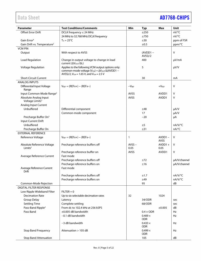
Data Sheet AD7768-CHIPS
Rev. 0 | Page 5 of 22
Parameter Test Conditions/Comments Min Typ Max Unit Offset Error Drift DCLK frequency ≤ 24 MHz ±250 nV/°C 24 MHz to 32.768 MHz DCLK frequency ±750 nV/°C Gain Error4 TA = 25°C ±30 ppm of FSR Gain Drift vs. Temperature2 ±0.5 ppm/°C
VCM PIN Output With respect to AVSS (AVDD1 −
AVSS)/2 V
Load Regulation Change in output voltage to change in load current (∆VOUT/∆IL)
400 μV/mA
Voltage Regulation Applies to the following VCM output options only: common-mode voltage (VCM) = ∆VOUT/∆(AVDD1 − AVSS)/2, VCM = 1.65 V, and VCM = 2.5 V
5 μV/V
Short-Circuit Current 30 mA ANALOG INPUTS
Differential Input Voltage Range
VREF = (REFx+) − (REFx−) −VREF +VREF V
Input Common-Mode Range2 AVSS AVDD1 V Absolute Analog Input
Voltage Limits2 AVSS AVDD1 V
Analog Input Current Unbuffered Differential component ±48 μA/V
Common-mode component 17 μA/V Precharge Buffer On5 −20 μA
Input Current Drift Unbuffered ±5 nA/V/°C Precharge Buffer On ±31 nA/°C
EXTERNAL REFERENCE Reference Voltage VREF = (REFx+) − (REFx−) 1 AVDD1 −
AVSS V
Absolute Reference Voltage Limits2
Precharge reference buffers off AVSS − 0.05
AVDD1 + 0.05
V
Precharge reference buffer on AVSS AVDD1 V Average Reference Current Fast mode Precharge reference buffers off ±72 μA/V/channel Precharge reference buffers on ±16 μA/V/channel Average Reference Current
Drift Fast mode
Precharge reference buffers off ±1.7 nA/V/°C Precharge reference buffers on ±49 nA/V/°C Common-Mode Rejection 95 dB
DIGITAL FILTER RESPONSE Low Ripple Wideband Filter FILTER = 0
Decimation Rate Up to six selectable decimation rates 32 1024 Group Delay Latency 34/ODR sec Settling Time Complete settling 68/ODR sec Pass-Band Ripple2 From dc to 102.4 kHz at 256 kSPS ±0.005 dB Pass Band ±0.005 dB bandwidth 0.4 × ODR Hz −0.1 dB bandwidth 0.409 ×
ODR Hz
−3 dB bandwidth 0.433 × ODR
Hz
Stop Band Frequency Attenuation > 105 dB 0.499 × ODR
Hz
Stop Band Attenuation 105 dB
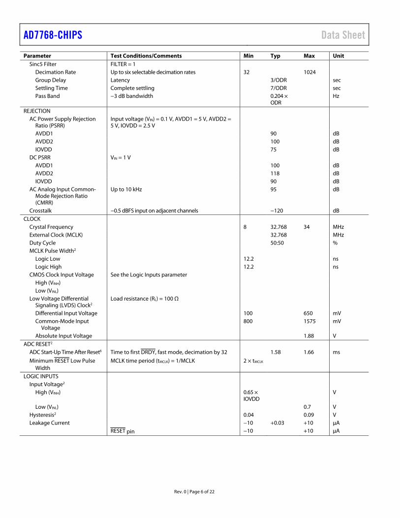
AD7768-CHIPS Data Sheet
Rev. 0 | Page 6 of 22
Parameter Test Conditions/Comments Min Typ Max Unit Sinc5 Filter FILTER = 1
Decimation Rate Up to six selectable decimation rates 32 1024 Group Delay Latency 3/ODR sec Settling Time Complete settling 7/ODR sec Pass Band −3 dB bandwidth 0.204 ×
ODR Hz
REJECTION AC Power Supply Rejection
Ratio (PSRR) Input voltage (VIN) = 0.1 V, AVDD1 = 5 V, AVDD2 = 5 V, IOVDD = 2.5 V
AVDD1 90 dB AVDD2 100 dB IOVDD 75 dB
DC PSRR VIN = 1 V AVDD1 100 dB AVDD2 118 dB IOVDD 90 dB
AC Analog Input Common-Mode Rejection Ratio (CMRR)
Up to 10 kHz 95 dB
Crosstalk −0.5 dBFS input on adjacent channels −120 dB CLOCK
Crystal Frequency 8 32.768 34 MHz External Clock (MCLK) 32.768 MHz Duty Cycle 50:50 % MCLK Pulse Width2
Logic Low 12.2 ns Logic High 12.2 ns
CMOS Clock Input Voltage See the Logic Inputs parameter High (VINH) Low (VINL)
Low Voltage Differential Signaling (LVDS) Clock2
Load resistance (RL) = 100 Ω
Differential Input Voltage 100 650 mV Common-Mode Input
Voltage 800 1575 mV
Absolute Input Voltage 1.88 V ADC RESET2
ADC Start-Up Time After Reset6 Time to first DRDY, fast mode, decimation by 32 1.58 1.66 ms
Minimum RESET Low Pulse Width
MCLK time period (tMCLK) = 1/MCLK 2 × tMCLK
LOGIC INPUTS Input Voltage2
High (VINH) 0.65 × IOVDD
V
Low (VINL) 0.7 V Hysteresis2 0.04 0.09 V Leakage Current −10 +0.03 +10 μA RESET pin −10 +10 μA
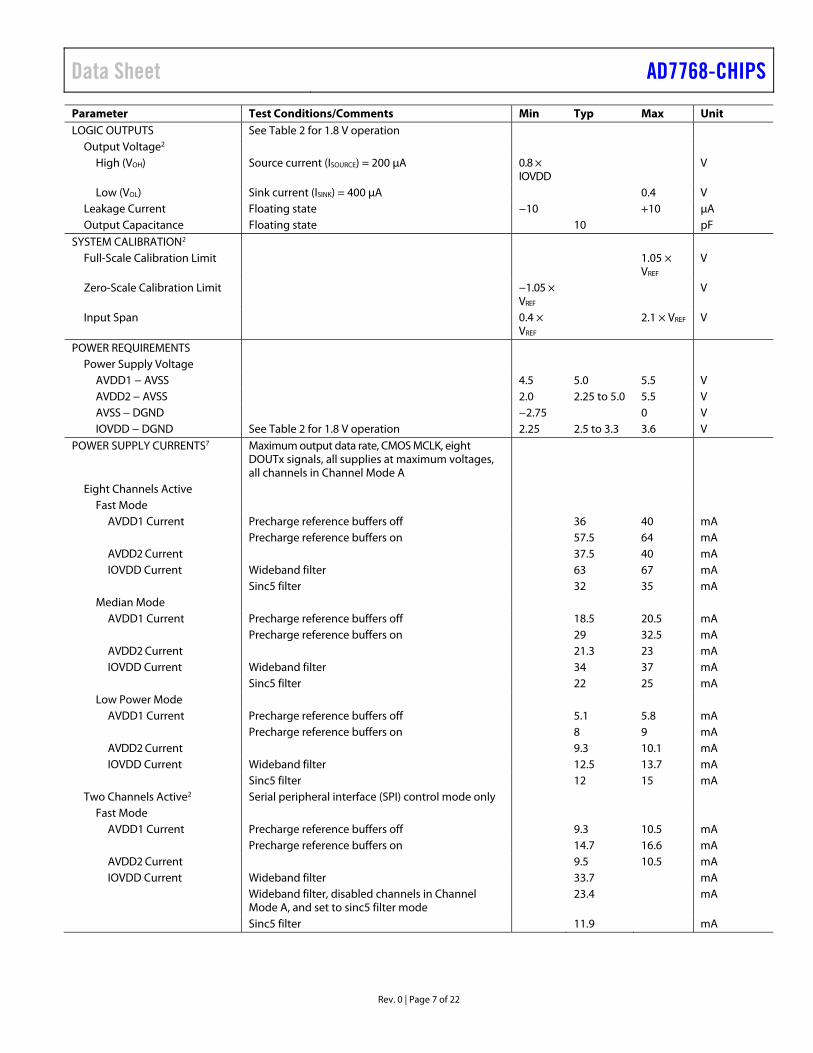
Data Sheet AD7768-CHIPS
Rev. 0 | Page 7 of 22
Parameter Test Conditions/Comments Min Typ Max Unit LOGIC OUTPUTS See Table 2 for 1.8 V operation
Output Voltage2 High (VOH) Source current (ISOURCE) = 200 μA 0.8 ×
IOVDD V
Low (VOL) Sink current (ISINK) = 400 μA 0.4 V Leakage Current Floating state −10 +10 μA Output Capacitance Floating state 10 pF
SYSTEM CALIBRATION2 Full-Scale Calibration Limit 1.05 ×
VREF V
Zero-Scale Calibration Limit −1.05 × VREF
V
Input Span 0.4 × VREF
2.1 × VREF V
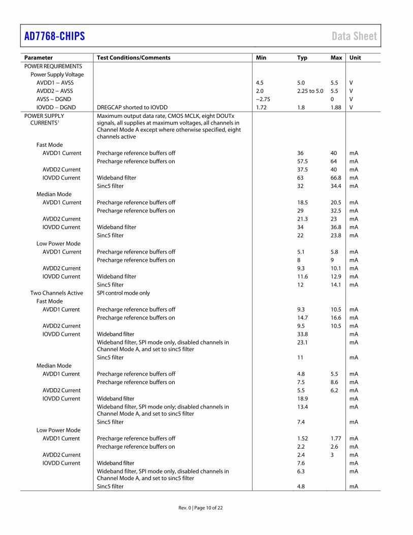
POWER REQUIREMENTS Power Supply Voltage
AVDD1 − AVSS 4.5 5.0 5.5 V AVDD2 − AVSS 2.0 2.25 to 5.0 5.5 V AVSS − DGND −2.75 0 V IOVDD − DGND See Table 2 for 1.8 V operation 2.25 2.5 to 3.3 3.6 V
POWER SUPPLY CURRENTS7 Maximum output data rate, CMOS MCLK, eight DOUTx signals, all supplies at maximum voltages, all channels in Channel Mode A
Eight Channels Active Fast Mode
AVDD1 Current Precharge reference buffers off 36 40 mA Precharge reference buffers on 57.5 64 mA AVDD2 Current 37.5 40 mA IOVDD Current Wideband filter 63 67 mA Sinc5 filter 32 35 mA
Median Mode AVDD1 Current Precharge reference buffers off 18.5 20.5 mA Precharge reference buffers on 29 32.5 mA AVDD2 Current 21.3 23 mA IOVDD Current Wideband filter 34 37 mA Sinc5 filter 22 25 mA
Low Power Mode AVDD1 Current Precharge reference buffers off 5.1 5.8 mA Precharge reference buffers on 8 9 mA AVDD2 Current 9.3 10.1 mA IOVDD Current Wideband filter 12.5 13.7 mA Sinc5 filter 12 15 mA
Two Channels Active2 Serial peripheral interface (SPI) control mode only Fast Mode
AVDD1 Current Precharge reference buffers off 9.3 10.5 mA Precharge reference buffers on 14.7 16.6 mA AVDD2 Current 9.5 10.5 mA IOVDD Current Wideband filter 33.7 mA Wideband filter, disabled channels in Channel
Mode A, and set to sinc5 filter mode 23.4 mA
Sinc5 filter 11.9 mA
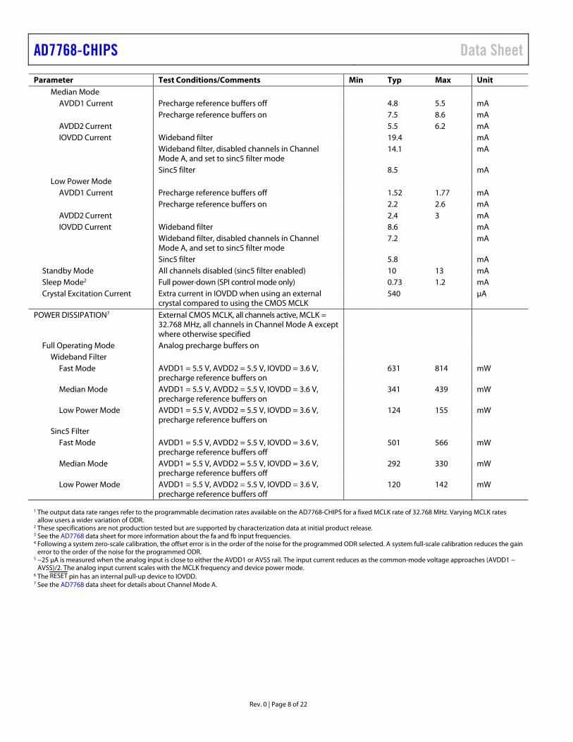
AD7768-CHIPS Data Sheet
Rev. 0 | Page 8 of 22
Parameter Test Conditions/Comments Min Typ Max Unit Median Mode
AVDD1 Current Precharge reference buffers off 4.8 5.5 mA Precharge reference buffers on 7.5 8.6 mA AVDD2 Current 5.5 6.2 mA IOVDD Current Wideband filter 19.4 mA Wideband filter, disabled channels in Channel
Mode A, and set to sinc5 filter mode 14.1 mA
Sinc5 filter 8.5 mA Low Power Mode
AVDD1 Current Precharge reference buffers off 1.52 1.77 mA Precharge reference buffers on 2.2 2.6 mA AVDD2 Current 2.4 3 mA IOVDD Current Wideband filter 8.6 mA Wideband filter, disabled channels in Channel
Mode A, and set to sinc5 filter mode 7.2 mA
Sinc5 filter 5.8 mA Standby Mode All channels disabled (sinc5 filter enabled) 10 13 mA Sleep Mode2 Full power-down (SPI control mode only) 0.73 1.2 mA Crystal Excitation Current Extra current in IOVDD when using an external
crystal compared to using the CMOS MCLK 540 μA
POWER DISSIPATION7 External CMOS MCLK, all channels active, MCLK = 32.768 MHz, all channels in Channel Mode A except where otherwise specified
Full Operating Mode Analog precharge buffers on Wideband Filter
Fast Mode AVDD1 = 5.5 V, AVDD2 = 5.5 V, IOVDD = 3.6 V, precharge reference buffers on
631 814 mW
Median Mode AVDD1 = 5.5 V, AVDD2 = 5.5 V, IOVDD = 3.6 V, precharge reference buffers on
341 439 mW
Low Power Mode AVDD1 = 5.5 V, AVDD2 = 5.5 V, IOVDD = 3.6 V, precharge reference buffers on
124 155 mW
Sinc5 Filter Fast Mode AVDD1 = 5.5 V, AVDD2 = 5.5 V, IOVDD = 3.6 V,
precharge reference buffers off 501 566 mW
Median Mode AVDD1 = 5.5 V, AVDD2 = 5.5 V, IOVDD = 3.6 V, precharge reference buffers off
292 330 mW
Low Power Mode AVDD1 = 5.5 V, AVDD2 = 5.5 V, IOVDD = 3.6 V, precharge reference buffers off
120 142 mW
1 The output data rate ranges refer to the programmable decimation rates available on the AD7768-CHIPS for a fixed MCLK rate of 32.768 MHz. Varying MCLK rates
allow users a wider variation of ODR. 2 These specifications are not production tested but are supported by characterization data at initial product release. 3 See the AD7768 data sheet for more information about the fa and fb input frequencies. 4 Following a system zero-scale calibration, the offset error is in the order of the noise for the programmed ODR selected. A system full-scale calibration reduces the gain
error to the order of the noise for the programmed ODR. 5 −25 μA is measured when the analog input is close to either the AVDD1 or AVSS rail. The input current reduces as the common-mode voltage approaches (AVDD1 −
AVSS)/2. The analog input current scales with the MCLK frequency and device power mode. 6 The RESETE pin has an internal pull-up device to IOVDD. 7 See the AD7768 data sheet for details about Channel Mode A.
Data Sheet AD7768-CHIPS
Rev. 0 | Page 9 of 22
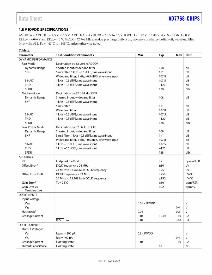
1.8 V IOVDD SPECIFICATIONS AVDD1A = AVDD1B = 4.5 V to 5.5 V, AVDD2A = AVDD2B = 2.0 V to 5.5 V, IOVDD = 1.72 V to 1.88 V, AVSS = DGND = 0 V, REFx+ = 4.096 V and REFx− = 0 V, MCLK = 32.768 MHz, analog precharge buffers on, reference precharge buffers off, wideband filter, fCHOP = fMOD/32, TA = −40°C to +105°C, unless otherwise noted.
Table 2. Parameter Test Conditions/Comments Min Typ Max Unit DYNAMIC PERFORMANCE
Fast Mode Decimation by 32, 256 kSPS ODR Dynamic Range Shorted input, wideband filter 108 dB SNR Sinc5 filter, 1 kHz, −0.5 dBFS, sine wave input 111 dB Wideband filter, 1 kHz, −0.5 dBFS, sine wave input 107.8 dB SINAD1 1 kHz, −0.5 dBFS, sine wave input 107.5 dB THD 1 kHz, −0.5 dBFS, sine wave input −120 dB SFDR 128 dBc
Median Mode Decimation by 32, 128 kHz ODR Dynamic Range Shorted input, wideband filter 108 dB SNR 1 kHz, −0.5 dBFS, sine wave input Sinc5 filter 111 dB Wideband filter 107.8 dB SINAD 1 kHz, −0.5 dBFS, sine wave input 107.5 dB THD 1 kHz, −0.5 dBFS, sine wave input −120 dB SFDR 128 dBc
Low Power Mode Decimation by 32, 32 kHz ODR Dynamic Range Shorted input, wideband filter 108 dB SNR Sinc5 filter, 1 kHz, −0.5 dBFS, sine wave input 111 dB Wideband filter, 1 kHz, −0.5 dBFS, sine wave input 107.8 dB SINAD 1 kHz, −0.5 dBFS, sine wave input 107.5 dB THD 1 kHz, −0.5 dBFS, sine wave input −120 dB SFDR 128 dBc
ACCURACY1 INL Endpoint method ±2 ppm of FSR Offset Error2 DCLK frequency ≤ 24 MHz ±50 μV 24 MHz to 32.768 MHz DCLK frequency ±75 μV Offset Error Drift DCLK frequency ≤ 24 MHz ±250 nV/°C 24 MHz to 32.768 MHz DCLK frequency ±750 nV/°C Gain Error2 TA = 25°C ±60 ppm/FSR Gain Drift vs.
Temperature ±0.5 ppm/°C
LOGIC INPUTS Input Voltage1
VINH 0.65 × IOVDD V VINL 0.4 V
Hysteresis1 0.04 0.2 V Leakage Current −10 +0.03 +10 μA RESETE pin −10 +10 μA
LOGIC OUTPUTS Output Voltage1
VOH ISOURCE = 200 μA 0.8 × IOVDD V VOL ISINK = 400 μA 0.4 V
Leakage Current Floating state −10 +10 μA Output Capacitance Floating state 10 pF
AD7768-CHIPS Data Sheet
Rev. 0 | Page 10 of 22
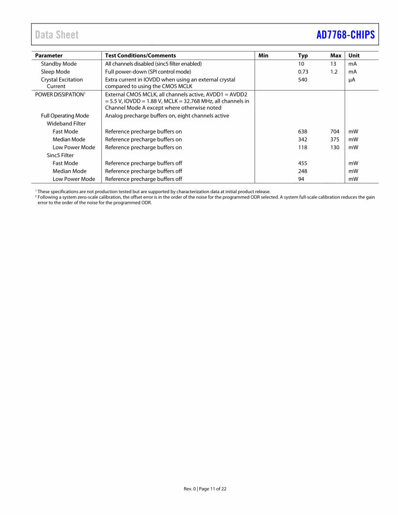
Parameter Test Conditions/Comments Min Typ Max Unit POWER REQUIREMENTS
Power Supply Voltage AVDD1 − AVSS 4.5 5.0 5.5 V AVDD2 − AVSS 2.0 2.25 to 5.0 5.5 V AVSS − DGND −2.75 0 V IOVDD − DGND DREGCAP shorted to IOVDD 1.72 1.8 1.88 V
POWER SUPPLY CURRENTS1
Maximum output data rate, CMOS MCLK, eight DOUTx signals, all supplies at maximum voltages, all channels in Channel Mode A except where otherwise specified, eight channels active
Fast Mode AVDD1 Current Precharge reference buffers off 36 40 mA
Precharge reference buffers on 57.5 64 mA AVDD2 Current 37.5 40 mA IOVDD Current Wideband filter 63 66.8 mA
Sinc5 filter 32 34.4 mAMedian Mode
AVDD1 Current Precharge reference buffers off 18.5 20.5 mA Precharge reference buffers on 29 32.5 mA
AVDD2 Current 21.3 23 mA IOVDD Current Wideband filter 34 36.8 mA
Sinc5 filter 22 23.8 mALow Power Mode
AVDD1 Current Precharge reference buffers off 5.1 5.8 mA Precharge reference buffers on 8 9 mA
AVDD2 Current 9.3 10.1 mA IOVDD Current Wideband filter 11.6 12.9 mA
Sinc5 filter 12 14.1 mATwo Channels Active SPI control mode only
Fast Mode AVDD1 Current Precharge reference buffers off 9.3 10.5 mA
Precharge reference buffers on 14.7 16.6 mA AVDD2 Current 9.5 10.5 mA IOVDD Current Wideband filter 33.8 mA
Wideband filter, SPI mode only, disabled channels in Channel Mode A, and set to sinc5 filter
23.1 mA
Sinc5 filter 11 mAMedian Mode
AVDD1 Current Precharge reference buffers off 4.8 5.5 mA Precharge reference buffers on 7.5 8.6 mA
AVDD2 Current 5.5 6.2 mA IOVDD Current Wideband filter 18.9 mA
Wideband filter, SPI mode only; disabled channels in Channel Mode A, and set to sinc5 filter
13.4 mA
Sinc5 filter 7.4 mALow Power Mode
AVDD1 Current Precharge reference buffers off 1.52 1.77 mA Precharge reference buffers on 2.2 2.6 mA
AVDD2 Current 2.4 3 mA IOVDD Current Wideband filter 7.6 mA
Wideband filter, SPI mode only, disabled channels in Channel Mode A, and set to sinc5 filter
6.3 mA
Sinc5 filter 4.8 mA
Data Sheet AD7768-CHIPS
Rev. 0 | Page 11 of 22
Parameter Test Conditions/Comments Min Typ Max Unit Standby Mode All channels disabled (sinc5 filter enabled) 10 13 mA Sleep Mode Full power-down (SPI control mode) 0.73 1.2 mA Crystal Excitation
Current Extra current in IOVDD when using an external crystal compared to using the CMOS MCLK
540 μA
POWER DISSIPATION1 External CMOS MCLK, all channels active, AVDD1 = AVDD2 = 5.5 V, IOVDD = 1.88 V, MCLK = 32.768 MHz, all channels in Channel Mode A except where otherwise noted
Full Operating Mode Analog precharge buffers on, eight channels active Wideband Filter
Fast Mode Reference precharge buffers on 638 704 mW Median Mode Reference precharge buffers on 342 375 mW Low Power Mode Reference precharge buffers on 118 130 mW
Sinc5 Filter Fast Mode Reference precharge buffers off 455 mW Median Mode Reference precharge buffers off 248 mW Low Power Mode Reference precharge buffers off 94 mW
1 These specifications are not production tested but are supported by characterization data at initial product release. 2 Following a system zero-scale calibration, the offset error is in the order of the noise for the programmed ODR selected. A system full-scale calibration reduces the gain
error to the order of the noise for the programmed ODR.
AD7768-CHIPS Data Sheet
Rev. 0 | Page 12 of 22
TIMING SPECIFICATIONS AVDD1A = AVDD1B = 5 V, AVDD2A = AVDD2B = 5 V, IOVDD = 2.25 V to 3.6 V, Input Logic 0 = DGND, Input Logic 1 = IOVDD, load capacitance (CLOAD) = 10 pF on the DCLK pin, CLOAD = 20 pF on the other digital outputs, REFx+ = 4.096 V, TA = −40°C to +105°C. See Table 5 and Table 6 for timing specifications at 1.8 V IOVDD. See the AD7768 data sheet for information about the RETIME_EN bit. tODR is the ODR time period.
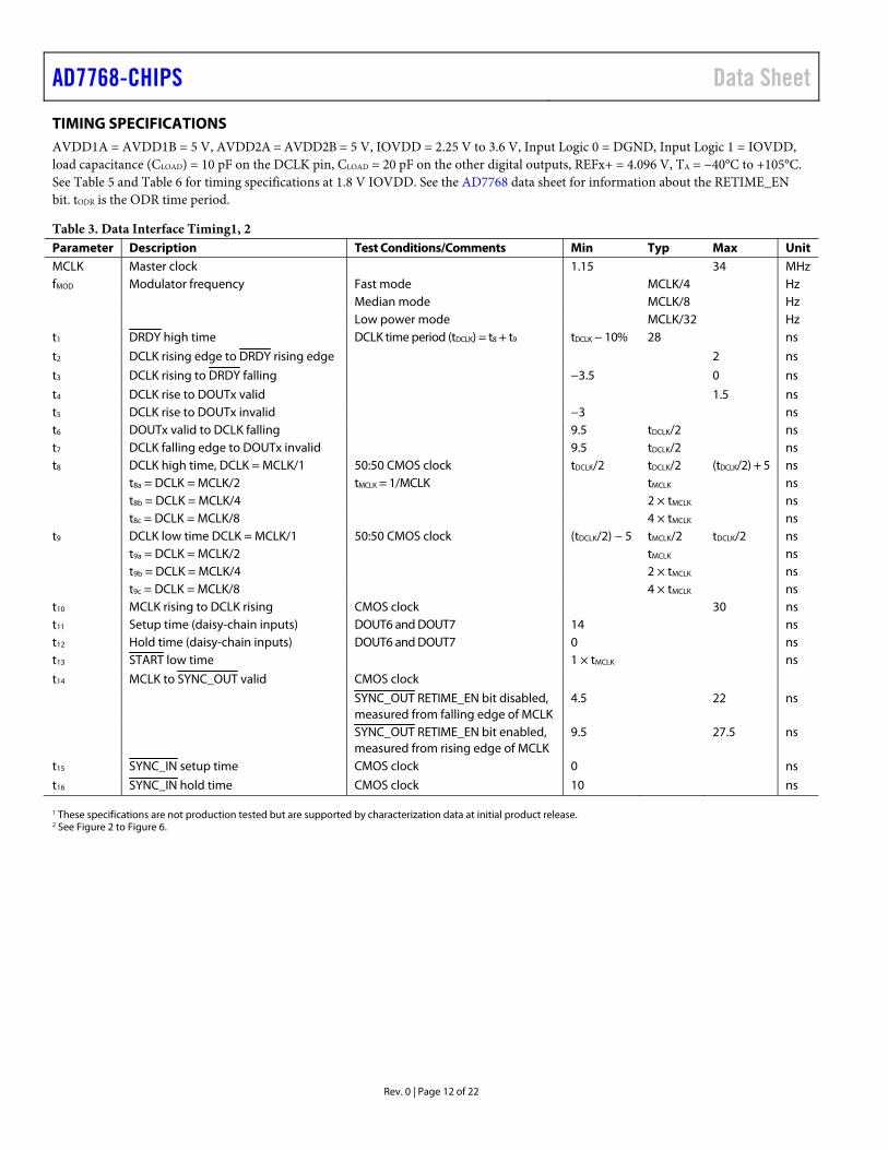
Table 3. Data Interface Timing1, 2 Parameter Description Test Conditions/Comments Min Typ Max Unit MCLK Master clock 1.15 34 MHz fMOD Modulator frequency Fast mode MCLK/4 Hz Median mode MCLK/8 Hz Low power mode MCLK/32 Hz t1 DRDY high time DCLK time period (tDCLK) = t8 + t9 tDCLK − 10% 28 ns
t2 DCLK rising edge to DRDY rising edge 2 ns
t3 DCLK rising to DRDY falling −3.5 0 ns
t4 DCLK rise to DOUTx valid 1.5 ns t5 DCLK rise to DOUTx invalid −3 ns t6 DOUTx valid to DCLK falling 9.5 tDCLK/2 ns t7 DCLK falling edge to DOUTx invalid 9.5 tDCLK/2 ns t8 DCLK high time, DCLK = MCLK/1 50:50 CMOS clock tDCLK/2 tDCLK/2 (tDCLK/2) + 5 ns t8a = DCLK = MCLK/2 tMCLK = 1/MCLK tMCLK ns t8b = DCLK = MCLK/4 2 × tMCLK ns t8c = DCLK = MCLK/8 4 × tMCLK ns t9 DCLK low time DCLK = MCLK/1 50:50 CMOS clock (tDCLK/2) − 5 tMCLK/2 tDCLK/2 ns t9a = DCLK = MCLK/2 tMCLK ns t9b = DCLK = MCLK/4 2 × tMCLK ns t9c = DCLK = MCLK/8 4 × tMCLK ns t10 MCLK rising to DCLK rising CMOS clock 30 ns t11 Setup time (daisy-chain inputs) DOUT6 and DOUT7 14 ns t12 Hold time (daisy-chain inputs) DOUT6 and DOUT7 0 ns t13 START low time 1 × tMCLK ns
t14 MCLK to SYNC_OUT valid CMOS clock
SYNC_OUT RETIME_EN bit disabled, measured from falling edge of MCLK
4.5 22 ns
SYNC_OUT RETIME_EN bit enabled, measured from rising edge of MCLK
9.5 27.5 ns
t15 SYNC_IN setup time CMOS clock 0 ns
t16 SYNC_IN hold time CMOS clock 10 ns 1 These specifications are not production tested but are supported by characterization data at initial product release. 2 See Figure 2 to Figure 6.
Data Sheet AD7768-CHIPS
Rev. 0 | Page 13 of 22
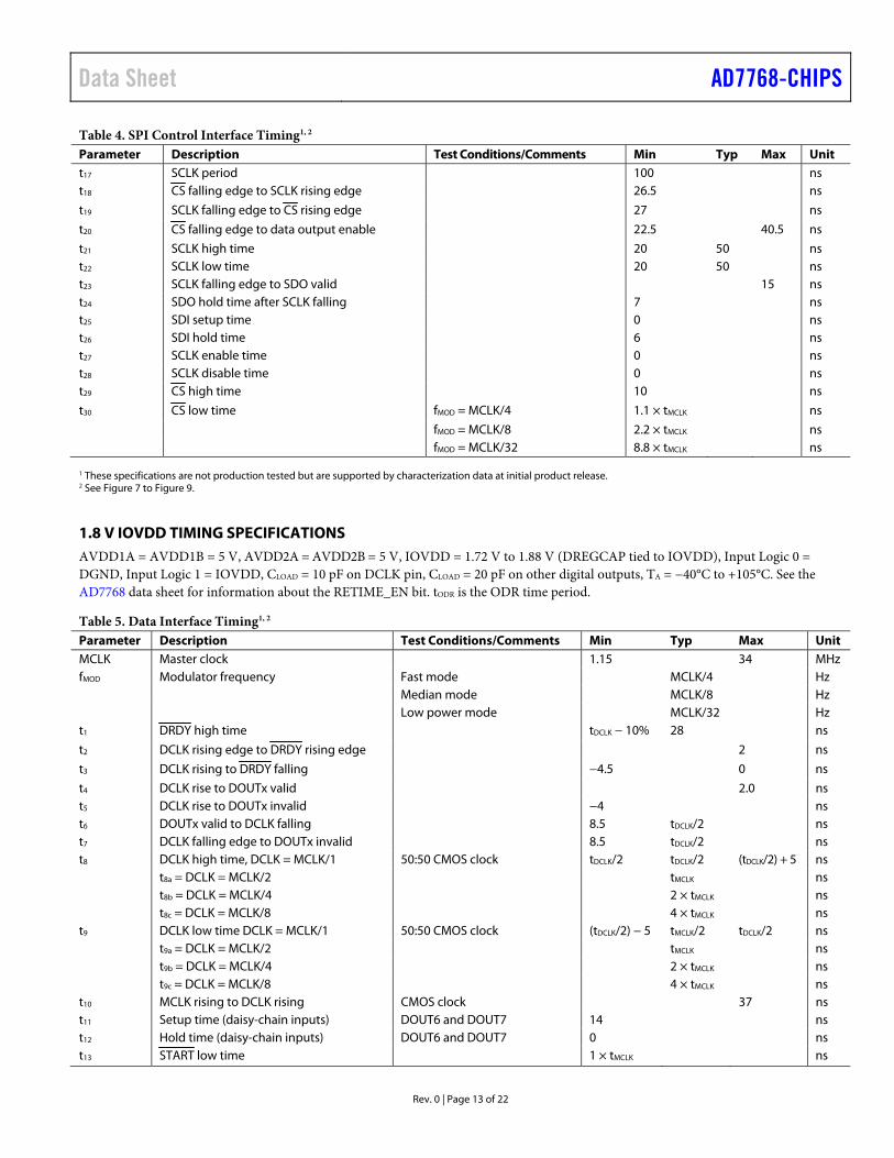
Table 4. SPI Control Interface Timing1, 2
Parameter Description Test Conditions/Comments Min Typ Max Unit t17 SCLK period 100 ns t18 CS falling edge to SCLK rising edge 26.5 ns
t19 SCLK falling edge to CS rising edge 27 ns
t20 CS falling edge to data output enable 22.5 40.5 ns
t21 SCLK high time 20 50 ns t22 SCLK low time 20 50 ns t23 SCLK falling edge to SDO valid 15 ns t24 SDO hold time after SCLK falling 7 ns t25 SDI setup time 0 ns t26 SDI hold time 6 ns t27 SCLK enable time 0 ns t28 SCLK disable time 0 ns t29 CS high time 10 ns
t30 CS low time fMOD = MCLK/4 1.1 × tMCLK ns
fMOD = MCLK/8 2.2 × tMCLK ns fMOD = MCLK/32 8.8 × tMCLK ns 1 These specifications are not production tested but are supported by characterization data at initial product release. 2 See Figure 7 to Figure 9.
1.8 V IOVDD TIMING SPECIFICATIONS AVDD1A = AVDD1B = 5 V, AVDD2A = AVDD2B = 5 V, IOVDD = 1.72 V to 1.88 V (DREGCAP tied to IOVDD), Input Logic 0 = DGND, Input Logic 1 = IOVDD, CLOAD = 10 pF on DCLK pin, CLOAD = 20 pF on other digital outputs, TA = −40°C to +105°C. See the AD7768 data sheet for information about the RETIME_EN bit. tODR is the ODR time period.
Table 5. Data Interface Timing1, 2 Parameter Description Test Conditions/Comments Min Typ Max Unit MCLK Master clock 1.15 34 MHz fMOD Modulator frequency Fast mode MCLK/4 Hz Median mode MCLK/8 Hz Low power mode MCLK/32 Hz t1 DRDY high time tDCLK − 10% 28 ns
t2 DCLK rising edge to DRDY rising edge 2 ns
t3 DCLK rising to DRDY falling −4.5 0 ns
t4 DCLK rise to DOUTx valid 2.0 ns t5 DCLK rise to DOUTx invalid −4 ns t6 DOUTx valid to DCLK falling 8.5 tDCLK/2 ns t7 DCLK falling edge to DOUTx invalid 8.5 tDCLK/2 ns t8 DCLK high time, DCLK = MCLK/1 50:50 CMOS clock tDCLK/2 tDCLK/2 (tDCLK/2) + 5 ns t8a = DCLK = MCLK/2 tMCLK ns t8b = DCLK = MCLK/4 2 × tMCLK ns t8c = DCLK = MCLK/8 4 × tMCLK ns t9 DCLK low time DCLK = MCLK/1 50:50 CMOS clock (tDCLK/2) − 5 tMCLK/2 tDCLK/2 ns t9a = DCLK = MCLK/2 tMCLK ns t9b = DCLK = MCLK/4 2 × tMCLK ns t9c = DCLK = MCLK/8 4 × tMCLK ns t10 MCLK rising to DCLK rising CMOS clock 37 ns t11 Setup time (daisy-chain inputs) DOUT6 and DOUT7 14 ns t12 Hold time (daisy-chain inputs) DOUT6 and DOUT7 0 ns t13 START low time 1 × tMCLK ns
AD7768-CHIPS Data Sheet
Rev. 0 | Page 14 of 22
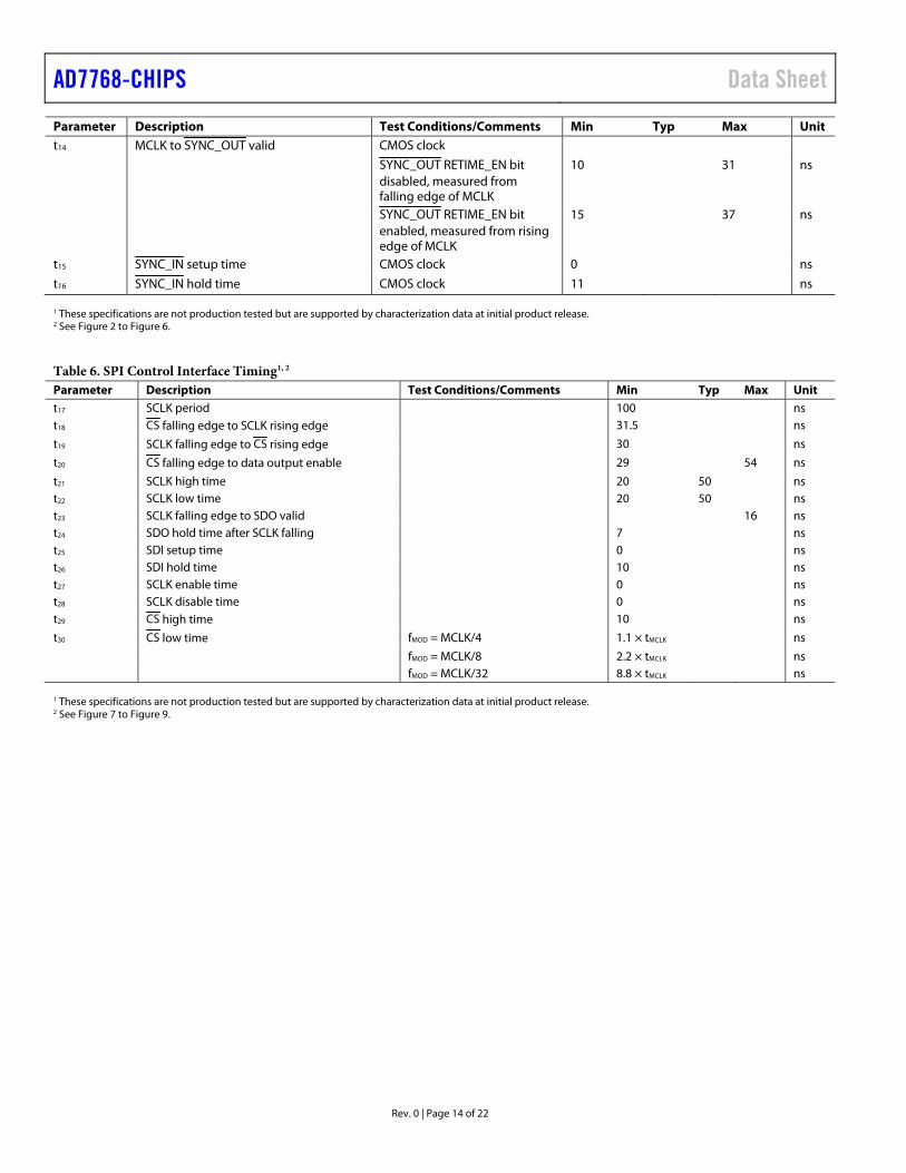
Parameter Description Test Conditions/Comments Min Typ Max Unit t14 MCLK to SYNC_OUT valid CMOS clock
SYNC_OUT RETIME_EN bit disabled, measured from falling edge of MCLK
10 31 ns
SYNC_OUT RETIME_EN bit enabled, measured from rising edge of MCLK
15 37 ns
t15 SYNC_IN setup time CMOS clock 0 ns
t16 SYNC_IN hold time CMOS clock 11 ns 1 These specifications are not production tested but are supported by characterization data at initial product release. 2 See Figure 2 to Figure 6.
Table 6. SPI Control Interface Timing1, 2 Parameter Description Test Conditions/Comments Min Typ Max Unit t17 SCLK period 100 ns t18 CS falling edge to SCLK rising edge 31.5 ns
t19 SCLK falling edge to CS rising edge 30 ns
t20 CS falling edge to data output enable 29 54 ns
t21 SCLK high time 20 50 ns t22 SCLK low time 20 50 ns t23 SCLK falling edge to SDO valid 16 ns t24 SDO hold time after SCLK falling 7 ns t25 SDI setup time 0 ns t26 SDI hold time 10 ns t27 SCLK enable time 0 ns t28 SCLK disable time 0 ns t29 CS high time 10 ns
t30 CS low time fMOD = MCLK/4 1.1 × tMCLK ns
fMOD = MCLK/8 2.2 × tMCLK ns fMOD = MCLK/32 8.8 × tMCLK ns 1 These specifications are not production tested but are supported by characterization data at initial product release. 2 See Figure 7 to Figure 9.
Data Sheet AD7768-CHIPS
Rev. 0 | Page 15 of 22
Timing Diagrams
DRDY
DCLK
LSB LSBMSBDOUTx
t1
tODR
t7
t6t5t4t3
t2 t8
t9
25518-002
Figure 2. Data Interface Timing Diagram
t8a
t8bt9a
MCLK
DCLK = MCLK/2
DCLK = MCLK/4
DCLK = MCLK/8
t10
t9b
t8c
t9c
25518-003
Figure 3. MCLK to DCLK Divider Timing Diagram
t11
tODR
t12
DRDY
DCLK
DOUT6AND
DOUT7
25518-004
Figure 4. Daisy-Chain Setup and Hold Timing Diagram
t13
t14
MCLK
START
SYNC_OUT
25518-005
Figure 5. Asynchronous START and SYNC_OUT Timing Diagram
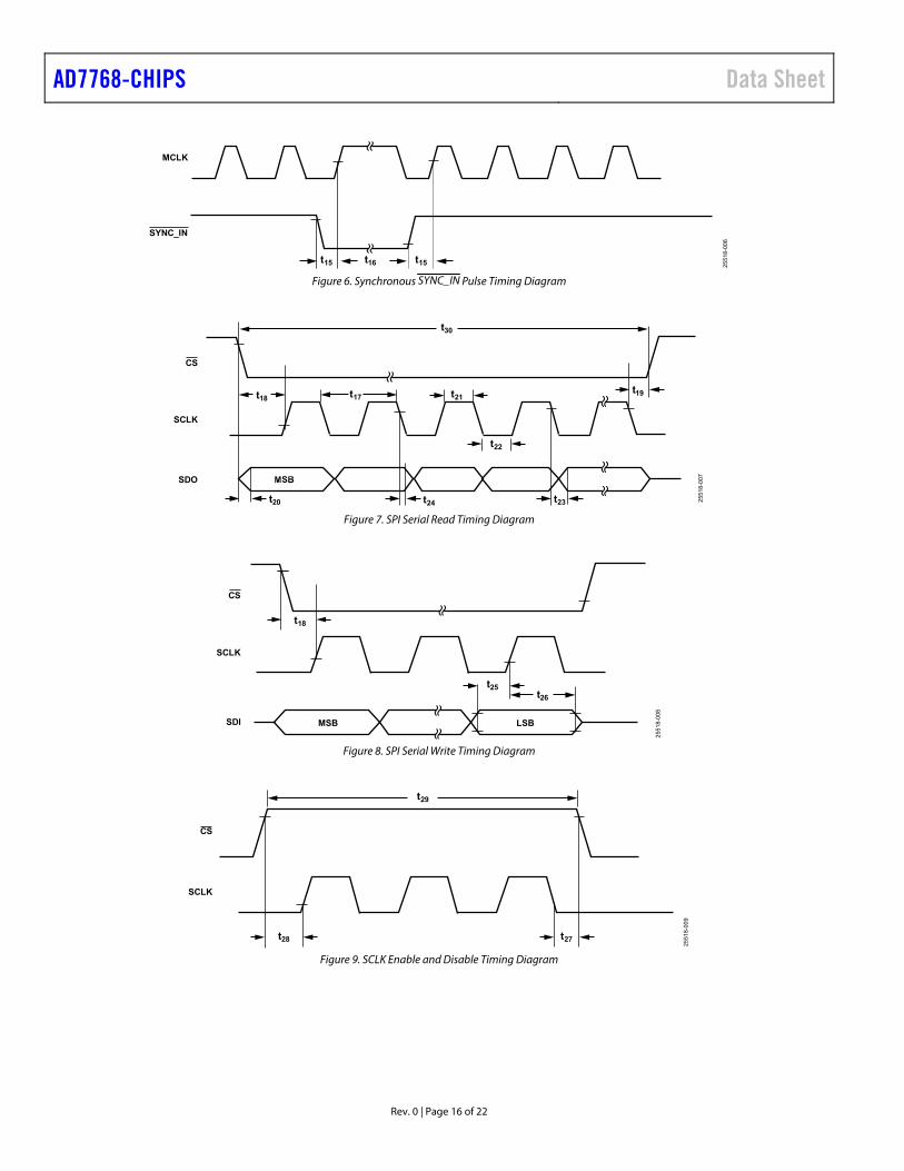
AD7768-CHIPS Data Sheet
Rev. 0 | Page 16 of 22
t16t15
MCLK
SYNC_IN
t15 25518-006
Figure 6. Synchronous SYNC_INE Pulse Timing Diagram
25518-007
CS
SCLK
SDO
t18 t17 t21
t30
t22
t23t24t20
19
Figure 7. SPI Serial Read Timing Diagram
CS
SCLK
SDI MSB LSB
t18
t25t26
25518-008
Figure 8. SPI Serial Write Timing Diagram
CS
SCLK
t28
t29
t27
25518-009
Figure 9. SCLK Enable and Disable Timing Diagram
Data Sheet AD7768-CHIPS
Rev. 0 | Page 17 of 22
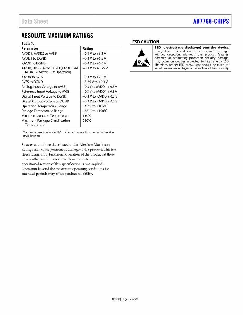
ABSOLUTE MAXIMUM RATINGS Table 7. Parameter Rating AVDD1, AVDD2 to AVSS1 −0.3 V to +6.5 V AVDD1 to DGND −0.3 V to +6.5 V IOVDD to DGND −0.3 V to +6.5 V IOVDD, DREGCAP to DGND (IOVDD Tied
to DREGCAP for 1.8 V Operation) −0.3 V to +2.25 V
IOVDD to AVSS −0.3 V to +7.5 V AVSS to DGND −3.25 V to +0.3 V Analog Input Voltage to AVSS −0.3 V to AVDD1 + 0.3 V Reference Input Voltage to AVSS −0.3 V to AVDD1 + 0.3 V Digital Input Voltage to DGND −0.3 V to IOVDD + 0.3 V Digital Output Voltage to DGND −0.3 V to IOVDD + 0.3 V Operating Temperature Range −40°C to +105°C Storage Temperature Range −65°C to +150°C Maximum Junction Temperature 150°C Maximum Package Classification
Temperature 260°C
1 Transient currents of up to 100 mA do not cause silicon controlled rectifier (SCR) latch-up.
Stresses at or above those listed under Absolute Maximum Ratings may cause permanent damage to the product. This is a stress rating only; functional operation of the product at these or any other conditions above those indicated in the operational section of this specification is not implied. Operation beyond the maximum operating conditions for extended periods may affect product reliability.
ESD CAUTION
AD7768-CHIPS Data Sheet
Rev. 0 | Page 18 of 22
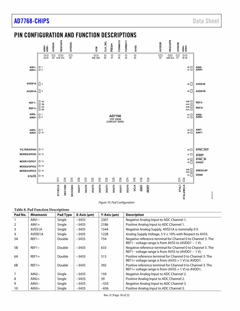
PIN CONFIGURATION AND FUNCTION DESCRIPTIONS
TOP VIEW(CIRCUIT SIDE)
AIN1+
AVSS1A
AVDD1A
AIN2–
REF1+
REF1–
AIN1–
AIN2+
AIN3–AIN3+
MODE0/GPIO0
MODE1/GPIO1
MODE2/GPIO2
MODE3/GPIO3
ST0/CS
FILTER/GPIO4
AD7768
AIN
0+A
IN0–
AV
SS
2A
RE
GC
AP
A
AV
DD
2A
VC
M
CL
K_S
EL
PIN
/SP
I
FO
RM
AT
0
FO
RM
AT
1
AV
SS
AV
DD
2B
RE
GC
AP
B
AV
SS
2B
AIN
4–A
IN4+
ST
1/S
CL
K
DE
C1/
SD
I
DE
C0/
SD
O
DO
UT
7
DO
UT
6
DO
UT
5
DO
UT
4
DO
UT
3
DO
UT
2
DO
UT
1
DO
UT
0
DC
LK
DR
DY
RE
SE
T
XT
AL
1
XT
AL
2/M
CL
K
AIN5+
AVSS1B
AVDD1B
AIN6–
REF2+
REF2–
AIN5–
AIN6+
AIN7–AIN7+
START
SYNC_INIOVDD
DREGCAP
DGND
SYNC_OUT
25518-010
12
3
5A5B6A6B
78
910
11
12
13
14
15
1617 18 19 20 21 22 23 24 25 26 27 28 29 30 31 32
4
33
34A
43A
44A
44B
43B
34B
36
37
38
3940
4142
4748
495054555657586364 59A61A61B 59B 52A52B 51
45
536062
46
35
Figure 10. Pad Configuration
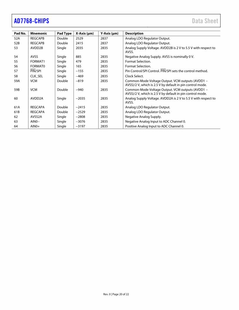
Table 8. Pad Function Descriptions Pad No. Mnemonic Pad Type X-Axis (μm) Y-Axis (μm) Description 1 AIN1− Single −3435 2307 Negative Analog Input to ADC Channel 1. 2 AIN1+ Single −3435 2186 Positive Analog Input to ADC Channel 1. 3 AVSS1A Single −3435 1544 Negative Analog Supply. AVSS1A is nominally 0 V. 4 AVDD1A Single −3435 1228 Analog Supply Voltage, 5 V ± 10% with Respect to AVSS. 5A REF1− Double −3435 754 Negative reference terminal for Channel 0 to Channel 3. The
REF1− voltage range is from AVSS to (AVDD1 − 1 V). 5B REF1− Double −3435 633 Negative reference terminal for Channel 0 to Channel 3. The
REF1− voltage range is from AVSS to (AVDD1 − 1 V). 6A REF1+ Double −3435 513 Positive reference terminal for Channel 0 to Channel 3. The
REF1+ voltage range is from (AVSS + 1 V) to AVDD1. 6B REF1+ Double −3435 392 Positive reference terminal for Channel 0 to Channel 3. The
REF1+ voltage range is from (AVSS + 1 V) to AVDD1. 7 AIN2− Single −3435 159 Negative Analog Input to ADC Channel 2. 8 AIN2+ Single −3435 39 Positive Analog Input to ADC Channel 2. 9 AIN3− Single −3435 −535 Negative Analog Input to ADC Channel 3. 10 AIN3+ Single −3435 −656 Positive Analog Input to ADC Channel 3.
Data Sheet AD7768-CHIPS
Rev. 0 | Page 19 of 22
Pad No. Mnemonic Pad Type X-Axis (μm) Y-Axis (μm) Description 11 FILTER/GPIO4 Single −3435 −1415 Filter Select/General-Purpose Input/Output 4. In pin control
mode, FILTER/GPIO4 selects the filter type. In SPI control mode, FILTER/GPIO4 can be used as a general-purpose input/output.
12 MODE0/GP1O0 Single −3435 −1629 Mode Selection/General-Purpose I/O Pin 0. 13 MODE1/GP1O1 Single −3435 −1948 Mode Selection/General-Purpose I/O Pin 1. 14 MODE2/GP1O2 Single −3435 −2162 Mode Selection/General-Purpose I/O Pin 2. 15 MODE3/GP1O3 Single −3435 −2376 Mode Selection/General-Purpose I/O Pin 3. 16 ST0/CS Single −3435 −2610 Standby 0/Chip Select Input.
17 ST1/SCLK Single −2610 −2835 Standby 1/Serial Clock Input. 18 DEC1/SDI Single −2296 −2835 Decimation Rate Control Input 1/Serial Data Input. 19 DEC0/SDO Single −1982 −2835 Decimation Rate Control Input 0/Serial Data Output. 20 DOUT7 Single −1668 −2835 Conversion Data Output 7. 21 DOUT6 Single −1355 −2835 Conversion Data Output 6. 22 DOUT5 Single −1041 −2835 Conversion Data Output 5. 23 DOUT4 Single −727 −2835 Conversion Data Output 4. 24 DOUT3 Single −413 −2835 Conversion Data Output 3. 25 DOUT2 Single −94 −2835 Conversion Data Output 2. 26 DOUT1 Single 219 −2835 Conversion Data Output 1. 27 DOUT0 Single 533 −2835 Conversion Data Output 0. 28 DCLK Single 847 −2835 ADC Conversion Data Clock. 29 DRDY Single 1161 −2835 Data Ready.
30 RESET Single 1475 −2835 Hardware Asynchronous Reset Input.
31 XTAL1 Single 2884 −2835 Input 1 for Crystal or Connection to an LVDS Clock. 32 XTAL2/MCLK Single 3089 −2835 Input 2 for CMOS or Crystal/LVDS Sampling Clock. 33 DGND Single 3435 −2565 Digital Ground. DGND is nominally 0 V. 34A DREGCAP Double 3437 −2435 Digital Low Dropout (LDO) Regulator Output. 34B DREGCAP Double 3437 −2323 Digital LDO Regulator Output. 35 IOVDD Single 3435 −1993 Digital Supply. IOVDD sets the logic levels for all interface pins. 36 SYNC_IN Single 3435 −1853 Synchronization Input. SYNC_IN receives the synchronous
signal from SYNC_OUT.
37 START Single 3435 −1639 Start Signal. The START pulse synchronizes the AD7768-CHIPS to other devices. The signal can be asynchronous
38 SYNC_OUT Single 3435 −1425 Synchronization Output. SYNC_OUT operates only when the START input is used.
39 AIN7+ Single 3435 −656 Positive Analog Input to ADC Channel 7. 40 AIN7− Single 3435 −535 Negative Analog Input to ADC Channel 7. 41 AIN6+ Single 3435 39 Positive Analog Input to ADC Channel 6. 42 AIN6− Single 3435 159 Negative Analog Input to ADC Channel 6. 43A REF2+ Double 3435 392 Reference Input, Positive. REF2+ is the positive reference
terminal for Channel 4 to Channel 7. 43B REF2+ Double 3435 513 Reference Input, Positive. REF2+ is the positive reference
terminal for Channel 4 to Channel 7. 44A REF2− Double 3435 633 Reference Input, Negative. REF2− is the negative reference
terminal for Channel 4 to Channel 7. 44B REF2− Double 3435 754 Reference Input, Negative. REF2− is the negative reference
terminal for Channel 4 to Channel 7. 45 AVDD1B Single 3435 1228 Analog Supply Voltage. AVDD1B is 5 V ± 10% with respect to
AVSS. 46 AVSS1B Single 3435 1544 Negative Analog Supply. AVSS1B is nominally 0 V. 47 AIN5+ Single 3435 2186 Positive Analog Input to ADC Channel 5. 48 AIN5− Single 3435 2307 Negative Analog Input to ADC Channel 5. 49 AIN4+ Single 3197 2835 Positive Analog Input to ADC Channel 4. 50 AIN4− Single 3076 2835 Negative Analog Input to ADC Channel 4. 51 AVSS2B Single 2808 2835 Negative Analog Supply. AVSS2B is nominally 0 V.
AD7768-CHIPS Data Sheet
Rev. 0 | Page 20 of 22
Pad No. Mnemonic Pad Type X-Axis (μm) Y-Axis (μm) Description 52A REGCAPB Double 2529 2837 Analog LDO Regulator Output. 52B REGCAPB Double 2415 2837 Analog LDO Regulator Output. 53 AVDD2B Single 2035 2835 Analog Supply Voltage. AVDD2B is 2 V to 5.5 V with respect to
AVSS. 54 AVSS Single 885 2835 Negative Analog Supply. AVSS is nominally 0 V. 55 FORMAT1 Single 479 2835 Format Selection. 56 FORMAT0 Single 165 2835 Format Selection. 57 PIN/SPI Single −155 2835 Pin Control/SPI Control. PIN/SPI sets the control method.
58 CLK_SEL Single −469 2835 Clock Select. 59A VCM Double −819 2835 Common-Mode Voltage Output. VCM outputs (AVDD1 −
AVSS)/2 V, which is 2.5 V by default in pin control mode. 59B VCM Double −940 2835 Common-Mode Voltage Output. VCM outputs (AVDD1 −
AVSS)/2 V, which is 2.5 V by default in pin control mode. 60 AVDD2A Single −2035 2835 Analog Supply Voltage. AVDD2A is 2 V to 5.5 V with respect to
AVSS. 61A REGCAPA Double −2415 2835 Analog LDO Regulator Output. 61B REGCAPA Double −2529 2835 Analog LDO Regulator Output. 62 AVSS2A Single −2808 2835 Negative Analog Supply. 63 AIN0− Single −3076 2835 Negative Analog Input to ADC Channel 0. 64 AIN0+ Single −3197 2835 Positive Analog Input to ADC Channel 0.
Data Sheet AD7768-CHIPS
Rev. 0 | Page 21 of 22
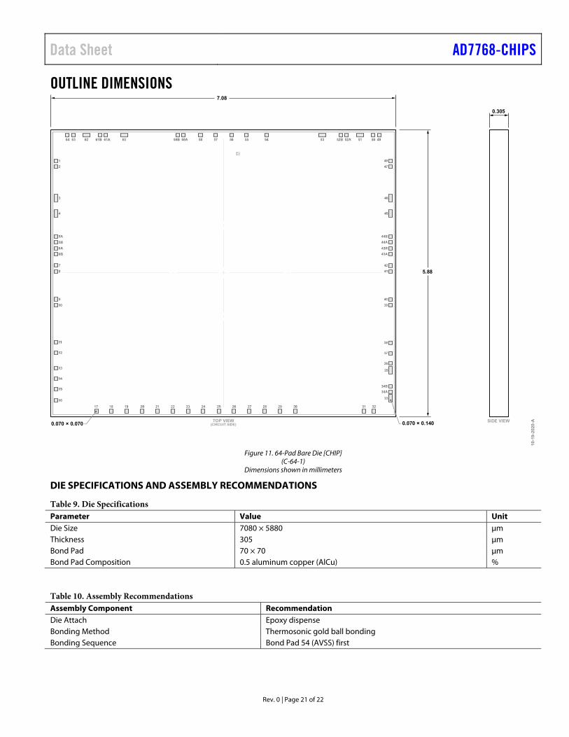
OUTLINE DIMENSIONS
10-1
9-20
20-A
0.305
SIDE VIEW
7.08
5.88
TOP VIEW(CIRCUIT SIDE)0.070 × 0.070 0.070 × 0.140
Figure 11. 64-Pad Bare Die [CHIP]
(C-64-1) Dimensions shown in millimeters
DIE SPECIFICATIONS AND ASSEMBLY RECOMMENDATIONS
Table 9. Die Specifications Parameter Value Unit Die Size 7080 × 5880 μm Thickness 305 μm Bond Pad 70 × 70 μm Bond Pad Composition 0.5 aluminum copper (AlCu) %
Table 10. Assembly Recommendations Assembly Component Recommendation Die Attach Epoxy dispense Bonding Method Thermosonic gold ball bonding Bonding Sequence Bond Pad 54 (AVSS) first
AD7768-CHIPS Data Sheet
Rev. 0 | Page 22 of 22
ORDERING GUIDE Model1 Temperature Range Package Description Package Option AD7768-CHIPS −40°C to +105°C 64-Pad Bare Die [CHIP], Waffle Pack C-64-1
1 AD7768-CHIPS is RoHS compliant.
©2021 Analog Devices, Inc. All rights reserved. Trademarks and registered trademarks are the property of their respective owners.
D25518-3/21(0)