8-bit Flash MCU - Farnell element14 · 2011-02-21 · – 11 Interrupt Sources With 4 Priority...
167
7663B–8051–03/07 1 Features • 80C52 Compatible – 8051 Instruction Compatible – Six 8-bit I/O Ports (64 pins or 68 Pins Versions) – Four 8-bit I/O Ports (44 Pins Version) – Three 16-bit Timer/Counters – 256 bytes Scratch Pad RAM – 11 Interrupt Sources With 4 Priority Levels • ISP (In-System Programming) Using Standard V CC Power Supply • Integrated Power Monitor (POR/PFD) to Supervise Internal Power Supply • Boot ROM Contains Serial Loader for In-System Programming • High-speed Architecture – In Standard Mode: 40 MHz (Vcc 2.7V to 5.5V, Both Internal and External Code Execution) 60 MHz (Vcc 4.5V to 5.5V and Internal Code Execution Only) – In X2 Mode (6 Clocks/Machine Cycle) 20 MHz (Vcc 2.7V to 5.5V, Both Internal and External Code Execution) 30 MHz (Vcc 4.5V to 5.5V and Internal Code Execution Only) • 128K bytes On-chip Flash Program/Data Memory – 128 bytes Page Write with auto-erase – 100k Write Cycles • On-chip 8192 bytes Expanded RAM (XRAM) – Software Selectable Size (0, 256, 512, 768, 1024, 1792, 2048, 4096, 8192 bytes) • Dual Data Pointer • Extended stack pointer to 512 bytes • Variable Length MOVX for Slow RAM/Peripherals • Improved X2 Mode with Independant Selection for CPU and Each Peripheral • Keyboard Interrupt Interface on Port 1 • SPI Interface (Master/Slave Mode) • 8-bit Clock Prescaler • Programmable Counter Array with: – High Speed Output – Compare/Capture – Pulse Width Modulator – Watchdog Timer Capabilities • Asynchronous Port Reset • Two Full Duplex Enhanced UART with Dedicated Internal Baud Rate Generator • Low EMI (inhibit ALE) • Hardware Watchdog Timer (One-time Enabled with Reset-Out), Power-Off Flag • Power Control Modes: Idle Mode, Power-down Mode • Power Supply: 2.7V to 5.5V • Temperature Ranges: Industrial (-40 to +85°C) • Packages: PLCC44, VQFP44, VQFP64 (1) Note: 1. Contact Atmel Sales for availability. 8-bit Flash Microcontroller AT89C51RE2
Transcript of 8-bit Flash MCU - Farnell element14 · 2011-02-21 · – 11 Interrupt Sources With 4 Priority...

7663B–8051–03/07
8-bit Flash
Microcontroller
AT89C51RE2
Features• 80C52 Compatible
– 8051 Instruction Compatible
– Six 8-bit I/O Ports (64 pins or 68 Pins Versions)
– Four 8-bit I/O Ports (44 Pins Version)
– Three 16-bit Timer/Counters
– 256 bytes Scratch Pad RAM
– 11 Interrupt Sources With 4 Priority Levels
• ISP (In-System Programming) Using Standard VCC Power Supply
• Integrated Power Monitor (POR/PFD) to Supervise Internal Power Supply
• Boot ROM Contains Serial Loader for In-System Programming
• High-speed Architecture
– In Standard Mode:
40 MHz (Vcc 2.7V to 5.5V, Both Internal and External Code Execution)
60 MHz (Vcc 4.5V to 5.5V and Internal Code Execution Only)
– In X2 Mode (6 Clocks/Machine Cycle)
20 MHz (Vcc 2.7V to 5.5V, Both Internal and External Code Execution)
30 MHz (Vcc 4.5V to 5.5V and Internal Code Execution Only)
• 128K bytes On-chip Flash Program/Data Memory
– 128 bytes Page Write with auto-erase
– 100k Write Cycles
• On-chip 8192 bytes Expanded RAM (XRAM)
– Software Selectable Size (0, 256, 512, 768, 1024, 1792, 2048, 4096, 8192 bytes)
• Dual Data Pointer
• Extended stack pointer to 512 bytes
• Variable Length MOVX for Slow RAM/Peripherals
• Improved X2 Mode with Independant Selection for CPU and Each Peripheral
• Keyboard Interrupt Interface on Port 1
• SPI Interface (Master/Slave Mode)
• 8-bit Clock Prescaler
• Programmable Counter Array with:
– High Speed Output
– Compare/Capture
– Pulse Width Modulator
– Watchdog Timer Capabilities
• Asynchronous Port Reset
• Two Full Duplex Enhanced UART with Dedicated Internal Baud Rate Generator
• Low EMI (inhibit ALE)
• Hardware Watchdog Timer (One-time Enabled with Reset-Out), Power-Off Flag
• Power Control Modes: Idle Mode, Power-down Mode
• Power Supply: 2.7V to 5.5V
• Temperature Ranges: Industrial (-40 to +85°C)
• Packages: PLCC44, VQFP44, VQFP64(1)
Note: 1. Contact Atmel Sales for availability.
1

Description
AT89C51RE2 is a high performance CMOS Flash version of the 80C51 CMOS single
chip 8-bit microcontroller. It contains a 128 Kbytes Flash memory block for program.
The 128 Kbytes Flash memory can be programmed either in parallel mode or in serial
mode with the ISP capability or with software. The programming voltage is internally
generated from the standard VCC pin.
The AT89C51RE2 retains all features of the Atmel 80C52 with 256 bytes of internal
RAM, a 10-source 4-level interrupt controller and three timer/counters.
In addition, the AT89C51RE2 has a Programmable Counter Array, an XRAM of 8192
bytes, a Hardware Watchdog Timer, SPI and Keyboard, two serial channels that facili-
tates multiprocessor communication (EUART), a speed improvement mechanism (X2
mode) and an extended stack mode that allows the stack to be extended in the lower
256 bytes of XRAM.
The fully static design of the AT89C51RE2 allows to reduce system power consumption
by bringing the clock frequency down to any value, even DC, without loss of data.
The AT89C51RE2 has 2 software-selectable modes of reduced activity and 8-bit clock
prescaler for further reduction in power consumption. In the Idle mode the CPU is frozen
while the peripherals and the interrupt system are still operating. In the power-down
mode the RAM is saved and all other functions are inoperative.
The added features of the AT89C51RE2 make it more powerful for applications that
need pulse width modulation, high speed I/O and counting capabilities such as alarms,
motor control, corded phones, smart card readers.
Table 1. Memory Size and I/O pins
Note: 1. For VQFP64 packages, please contact Atmel sales offices for availability.
AT89C51RE2 Flash (bytes) XRAM (bytes)
TOTAL RAM
(bytes) I/O
PLCC44
VQFP44128K 8192 8192 + 256 34
VQFP64 (1) 128K 8192 8192 + 256 50
2 AT89C51RE27663B–8051–03/07

AT89C51RE2
Block Diagram
Figure 1. Block Diagram
Timer 0 INT
RAM256x8
T0
T1
Rx
D_0
TxD
_0
WR
RD
EA
PSEN
ALE/
XTALA2
XTALA1
EUART
CPU
Timer 1
INT
1
Ctrl
INT
0
(2)
(2)
C51 CORE
(2) (2) (2) (2)
Port 0
P0
Port 1Port 2 Port 3
P1
P2
P3
XRAM8192 x 8
IB-bus
PCA
RE
SE
T
PROG
WatchDog
PC
A
EC
I
Vss
VC
C
(2)(2) (1)
(1): Alternate function of Port 1
(2): Alternate function of Port 3
(1)
Timer2
T2
EX
T2
(1) (1)
Flash128Kx8 Keyboard
(1)
Key
bo
ard
MIS
O
MO
SI
SC
K
SS
(3): Alternate function of Port 6
(3) (3)
Port4
P4
(1) (1) (1)(1)
BOOT4K x8
ROM
Regulator
POR / PFD
Port 5
P5
Parallel I/O Ports &
External Bus SPI
POR
PFD
XTALB2
XTALB1(1)
EUART_1
Rx
D_1
TxD
_1
3
7663B–8051–03/07

Pin Configurations
43 42 41 40 3944 38 37 36 35 34
P1.4
/CE
X1
P1.0
/T2/X
TA
LB
1
P1.1
/T2E
X/S
S
P1.3
/CE
X0
P1.2
/EC
I
Rx_O
CD
VC
C
P0.0
/AD
0
P0.2
/AD
2
P0.3
/AD
3
P0.1
/AD
1
P0.4/AD4
P0.6/AD6
P0.5/AD5
P0.7/AD7
ALE
PSEN
EA
P6.1/TxD_1
P2.7/A15
P2.5/A13
P2.6/A14
P1.5/CEX2/MISO
P1.6/CEX3/SCK
P1.7/CEX4/MOSI
RST
P3.0/RxD_0
P6.0/RxD_1
P3.1/TxD_0
P3.2/INT0
P3.3/INT1
P3.4/T0
P3.5/T1
P3.6
/WR
P3.7
/RD
XTA
L2
XTA
L1
VS
S
P2.0
/A8
P2.1
/A9
P2.2
/A10
P2.3
/A11
P2.4
/A12
Tx_O
CD
12 13 17161514 201918 21 22
33
32
31
30
29
28
27
26
25
24
23
1
2
3
4
5
6
7
8
9
10
11
VQFP44
PLCC44
AT89C51RE2
AT89C51RE2
18 19 23222120 262524 27 28
5 4 3 2 1 6 44 43 42 41 40
P1.4
/CE
X1
P1.0
/T2
P1.1
/T2E
X/S
S
P1.3
/CE
X0
P1.2
/EC
I
Rx_
OC
D
VC
C
P0.0
/AD
0
P0.2
/AD
2
P0.1
/AD
1
P0.4/AD4
P0.6/AD6
P0.5/AD5
P0.7/AD7
ALE
PSEN
EA
P6.1/TxD_1
P2.7/A15
P2.5/A13
P2.6/A14
P3.6
/WR
P3.7
/RD
XTA
L2
XTA
L1
VS
S
P2.0
/A8
P2.1
/A9
P2
.2/A
10
P2
.3/A
11
P2
.4/A
12
P1.5/CEX2/MISO
P1.6/CEX3/SCK
P1.7/CEx4/MOSI
RST
P3.0/RxD_0
P6.0/RxD_1
P3.1/TxD_0
P3.2/INT0
P3.3/INT1
P3.4/T0
P3.5/T1
P0
.3/A
D3
Tx_
OC
D
7
8
9
10
11
12
13
14
15
16
17
39
38
37
36
35
34
33
32
31
30
29
4 AT89C51RE27663B–8051–03/07

AT89C51RE2
NIC: Not Internaly Connected
54
53
52
51
50
49
VQFP64
P0.4
/AD
4
P5.4
P5
.3
P0.5
/AD
5
P0
.6/A
D6
P0.7
/AD
7
EA
#
P6.1
/TxD
_1
ALE
PS
EN
#
P1.5
/CE
X2/M
ISO
P1
.6/C
EX
3/S
CK
P1
.7/A
17
/CE
X4
/MO
SI
RS
T
NIC
NIC
NIC
P3
.0/R
xD
P6.0
/RxD
_1
P4
.2
48
47
46
45
44
43
42
41
39
40
1
2
3
4
5
6
7
8
10
9
17
18
19
20
21
22
23
24
25
26
64
63
62
61
60
59
58
57
56
55
P2.4/A12
P2.3/A11
P4.7
P2.2/A10
P2.1/A9
Tx_OCD
P4.6
P2.0/A8
VSS
P4.5
P5.5
P0.3/AD3
P0.2/AD2
P5.6
P0.1/AD1
P0.0/AD0
P5.7
VCC
Rx_OCD
P1.0/T2
11
12
13
16
15
14
P4.0
P1.1/T2EX/SS#
P1.2/ECI
P1.3/CEX0
P4.1
P1.4/CEX1
38
37
36
33
34
35
P3.7/RD#
XTAL2
XTAL1
P4.4
P3.6/WR#
P4.3
NIC
P3
.1/T
xD
P3.2
/IN
T0#
P3.3
/IN
T1#
P3.4
/T0
P3.5
/T1
27
28
29
30
31
32
P2.7
/A15
P2
.6/A
14
P5.2
P5
.1
P2
.5/A
13
P5.0
AT89C51RE2
5
7663B–8051–03/07

Table 2. Pin Description
Mnemonic
Pin Number
Type Name and FunctionLCC VQFP 1.4
VSS 22 16 I Ground: 0V reference
Vss1 39 I Optional Ground: Contact the Sales Office for ground connection.
VCC 44 38 I Power Supply: This is the power supply voltage for normal, idle and power-down operation
P0.0-P0.7 43-36 37-30 I/O Port 0: Port 0 is an open-drain, bidirectional I/O port. Port 0 pins that have 1s written to them
float and can be used as high impedance inputs. Port 0 must be polarized to VCC or VSS in
order to prevent any parasitic current consumption. Port 0 is also the multiplexed low-order
address and data bus during access to external program and data memory. In this
application, it uses strong internal pull-up when emitting 1s. Port 0 also inputs the code bytes
during EPROM programming. External pull-ups are required during program verification
during which P0 outputs the code bytes.
P1.0-P1.7 2-9 40-44
1-3
I/O Port 1: Port 1 is an 8-bit bidirectional I/O port with internal pull-ups. Port 1 pins that have 1s
written to them are pulled high by the internal pull-ups and can be used as inputs. As inputs,
Port 1 pins that are externally pulled low will source current because of the internal pull-ups.
Port 1 also receives the low-order address byte during memory programming and
verification.
Alternate functions for TSC8x54/58 Port 1 include:
2 40 I/O T2 (P1.0): Timer/Counter 2 external count input/Clockout
3 41 I T2EX (P1.1): Timer/Counter 2 Reload/Capture/Direction Control
4 42 I ECI (P1.2): External Clock for the PCA
5 43 I/O CEX0 (P1.3): Capture/Compare External I/O for PCA module 0
6 44 I/O CEX1 (P1.4): Capture/Compare External I/O for PCA module 1
7 1 I/O CEX2 (P1.5): Capture/Compare External I/O for PCA module 2
8 2 I/O CEX3 (P1.6): Capture/Compare External I/O for PCA module 3
9 3 I/O CEX4 (P1.7): Capture/Compare External I/O for PCA module 4
P2.0-P2.7 24-31 18-25 I/O Port 2: Port 2 is an 8-bit bidirectional I/O port with internal pull-ups. Port 2 pins that have 1s
written to them are pulled high by the internal pull-ups and can be used as inputs. As inputs,
Port 2 pins that are externally pulled low will source current because of the internal pull-ups.
Port 2 emits the high-order address byte during fetches from external program memory and
during accesses to external data memory that use 16-bit addresses (MOVX @DPTR).In this
application, it uses strong internal pull-ups emitting 1s. During accesses to external data
memory that use 8-bit addresses (MOVX @Ri), port 2 emits the contents of the P2 SFR.
Some Port 2 pins receive the high order address bits during EPROM programming and
verification:
P2.0 to P2.5 for RB devices
P2.0 to P2.6 for RC devices
P2.0 to P2.7 for RD devices.
P3.0-P3.7 11,
13-19
5,
7-13
I/O Port 3: Port 3 is an 8-bit bidirectional I/O port with internal pull-ups. Port 3 pins that have 1s
written to them are pulled high by the internal pull-ups and can be used as inputs. As inputs,
Port 3 pins that are externally pulled low will source current because of the internal pull-ups.
Port 3 also serves the special features of the 80C51 family, as listed below.
11 5 I RXD_0 (P3.0): Serial input port
13 7 O TXD_0 (P3.1): Serial output port
14 8 I INT0 (P3.2): External interrupt 0
6 AT89C51RE27663B–8051–03/07

AT89C51RE2
15 9 I INT1 (P3.3): External interrupt 1
16 10 I T0 (P3.4): Timer 0 external input
17 11 I T1 (P3.5): Timer 1 external input
18 12 O WR (P3.6): External data memory write strobe
19 13 O RD (P3.7): External data memory read strobe
P6.0-P6.112,34 6, 28
Port 6: Port 6 is an 2-bit bidirectional I/O port with internal pull-ups. Port 6 pins that have 1s
written to them are pulled high by the internal pull-ups and can be used as inputs. As inputs,
Port 6 pins that are externally pulled low will source current because of the internal pull-ups.
Port 6 also serves some special features as listed below.
12 6 I RXD_1 (P6.0): Serial input port
34 28 O TXD_1 (P6.1): Serial output port
Reset 10 4 I/O Reset: A high on this pin for two machine cycles while the oscillator is running, resets the
device. An internal diffused resistor to VSS permits a power-on reset using only an external
capacitor to VCC. This pin is an output when the hardware watchdog forces a system reset.
ALE/PROG 33 27 O (I) Address Latch Enable/Program Pulse: Output pulse for latching the low byte of the
address during an access to external memory. In normal operation, ALE is emitted at a
constant rate of 1/6 (1/3 in X2 mode) the oscillator frequency, and can be used for external
timing or clocking. Note that one ALE pulse is skipped during each access to external data
memory. This pin is also the program pulse input (PROG) during Flash programming. ALE
can be disabled by setting SFR’s AUXR.0 bit. With this bit set, ALE will be inactive during
internal fetches.
PSEN 32 26 O Program Store ENable: The read strobe to external program memory. When executing
code from the external program memory, PSEN is activated twice each machine cycle,
except that two PSEN activations are skipped during each access to external data memory.
PSEN is not activated during fetches from internal program memory.
EA 35 29 I External Access Enable: EA must be externally held low to enable the device to fetch code
from external program memory locations 0000H to FFFFH (RD). If security level 1 is
programmed, EA will be internally latched on Reset.
XTAL1 21 15 ICrystal 1: Input to the inverting oscillator amplifier and input to the internal clock generator
circuits.
XTAL2 20 14 O Crystal 2: Output from the inverting oscillator amplifier
Tx_OCD 23 17 O Tx_OCD: On chip debug Serial output port
Rx_OCD 1 39 I Rx_OCD: On chip debug Serial input port
Mnemonic
Pin Number
Type Name and FunctionLCC VQFP 1.4
7
7663B–8051–03/07

SFR Mapping The Special Function Registers (SFRs) of the AT89C51RE2 fall into the following
categories:
• C51 core registers: ACC, B, DPH, DPL, PSW, SP
• I/O port registers: P0, P1, P2, P3, P4, P5, P6
• Timer registers: T2CON, T2MOD, TCON, TH0, TH1, TH2, TMOD, TL0, TL1, TL2,
RCAP2L, RCAP2H
• Serial I/O port registers: SADDR_0, SADEN_0, SBUF_0, SCON_0, SADDR_1,
SADEN_1, SBUF_1, SCON_1,
• PCA (Programmable Counter Array) registers: CCON, CCAPMx, CL, CH, CCAPxH,
CCAPxL (x: 0 to 4)
• Power and clock control registers: PCON, CKAL, CKCON0_1
• Hardware Watchdog Timer registers: WDTRST, WDTPRG
• Interrupt system registers: IE0, IPL0, IPH0, IE1, IPL1, IPH1
• Keyboard Interface registers: KBE, KBF, KBLS
• SPI registers: SPCON, SPSTR, SPDAT
• BRG (Baud Rate Generator) registers: BRL_0, BRL_1, BDRCON_0, BDRCON_1
• Memory register: FCON, FSTA
• Clock Prescaler register: CKRL
• Others: AUXR, AUXR1, CKCON0, CKCON1, BMSEL
8 AT89C51RE27663B–8051–03/07

AT89C51RE2
Table 3. C51 Core SFRs
Mnemonic Add Name 7 6 5 4 3 2 1 0
ACC E0h Accumulator
B F0h B Register
PSW D0h Program Status Word CY AC F0 RS1 RS0 OV F1 P
SP 81h Stack Pointer
DPL 82h Data Pointer Low byte
DPH 83h Data Pointer High byte
Table 4. System Management SFRs
Mnemonic Add Name 7 6 5 4 3 2 1 0
PCON 87h Power Control SMOD1_0 SMOD0_0 - POF GF1 GF0 PD IDL
AUXR 8Eh Auxiliary Register 0 - - M0 XRS2 XRS1 XRS0EXTRA
MAO
AUXR1 A2h Auxiliary Register 1 EES SP9 U2 - GF2 0 - DPS
CKRL 97h Clock Reload Register - - - - - - - -
BMSEL 92h Bank Memory Select MBO2 MBO1 MBO0 - FBS2 FBS1 FBS0
CKCON0 8Fh Clock Control Register 0 - WDX2 PCAX2 SIX2_0 T2X2 T1X2 T0X2 X2
CKCON1 AFh Clock Control Register 1 - - - - - - SIX2_1 SPIX2
Table 5. Interrupt SFRs
Mnemonic Add Name 7 6 5 4 3 2 1 0
IEN0 A8h Interrupt Enable Control 0 EA EC ET2 ES ET1 EX1 ET0 EX0
IEN1 B1h Interrupt Enable Control 1 - - - - ES_1 ESPI ETWI EKBD
IPH0 B7h Interrupt Priority Control High 0 - PPCH PT2H PSH PT1H PX1H PT0H PX0H
IPL0 B8h Interrupt Priority Control Low 0 - PPCL PT2L PSL PT1L PX1L PT0L PX0L
IPH1 B3h Interrupt Priority Control High 1 - - - - PSH_1 SPIH IE2CH KBDH
IPL1 B2h Interrupt Priority Control Low 1 - - - - PSL_1 SPIL IE2CL KBDL
Table 6. Port SFRs
Mnemonic Add Name 7 6 5 4 3 2 1 0
P0 80h 8-bit Port 0
P1 90h 8-bit Port 1
P2 A0h 8-bit Port 2
P3 B0h 8-bit Port 3
P4 C0h 8-bit Port 4
9
7663B–8051–03/07

P5 E8h 8-bit Port 5
P6 F8h 2-bit Port 5 - - - - - -
Table 6. Port SFRs
Mnemonic Add Name 7 6 5 4 3 2 1 0
Table 7. Flash and EEPROM Data Memory SFR
Mnemonic Add Name 7 6 5 4 3 2 1 0
FCON D1h Flash Controller Control FPL3 FPL2 FPL1 FPL0 FPS FMOD2 FMOD1 FMOD0
FSTA D3h Flash Controller Status FMR FSE FLOAD FBUSY
Table 8. Timer SFRs
Mnemonic Add Name 7 6 5 4 3 2 1 0
TCON 88h Timer/Counter 0 and 1 Control TF1 TR1 TF0 TR0 IE1 IT1 IE0 IT0
TMOD 89h Timer/Counter 0 and 1 Modes GATE1 C/T1# M11 M01 GATE0 C/T0# M10 M00
TL0 8Ah Timer/Counter 0 Low Byte
TH0 8Ch Timer/Counter 0 High Byte
TL1 8Bh Timer/Counter 1 Low Byte
TH1 8Dh Timer/Counter 1 High Byte
WDTRST A6h WatchDog Timer Reset
WDTPRG A7h WatchDog Timer Program - - - - - WTO2 WTO1 WTO0
T2CON C8h Timer/Counter 2 control TF2 EXF2 RCLK TCLK EXEN2 TR2 C/T2# CP/RL2#
T2MOD C9h Timer/Counter 2 Mode - - - - - - T2OE DCEN
RCAP2H CBhTimer/Counter 2 Reload/Capture
High byte
RCAP2L CAhTimer/Counter 2 Reload/Capture
Low byte
TH2 CDh Timer/Counter 2 High Byte
TL2 CCh Timer/Counter 2 Low Byte
Table 9. PCA SFRs
Mnemo
-nic Add Name 7 6 5 4 3 2 1 0
CCON D8h PCA Timer/Counter Control CF CR - CCF4 CCF3 CCF2 CCF1 CCF0
CMOD D9h PCA Timer/Counter Mode CIDL WDTE - - - CPS1 CPS0 ECF
CL E9h PCA Timer/Counter Low byte
10 AT89C51RE27663B–8051–03/07

AT89C51RE2
CH F9h PCA Timer/Counter High byte
CCAPM0
CCAPM1
CCAPM2
CCAPM3
CCAPM4
DAh
DBh
DCh
DDh
DEh
PCA Timer/Counter Mode 0
PCA Timer/Counter Mode 1
PCA Timer/Counter Mode 2
PCA Timer/Counter Mode 3
PCA Timer/Counter Mode 4
-
ECOM0
ECOM1
ECOM2
ECOM3
ECOM4
CAPP0
CAPP1
CAPP2
CAPP3
CAPP4
CAPN0
CAPN1
CAPN2
CAPN3
CAPN4
MAT0
MAT1
MAT2
MAT3
MAT4
TOG0
TOG1
TOG2
TOG3
TOG4
PWM0
PWM1
PWM2
PWM3
PWM4
ECCF0
ECCF1
ECCF2
ECCF3
ECCF4
CCAP0H
CCAP1H
CCAP2H
CCAP3H
CCAP4H
FAh
FBh
FCh
FDh
FEh
PCA Compare Capture Module 0 H
PCA Compare Capture Module 1 H
PCA Compare Capture Module 2 H
PCA Compare Capture Module 3 H
PCA Compare Capture Module 4 H
CCAP0H7
CCAP1H7
CCAP2H7
CCAP3H7
CCAP4H7
CCAP0H6
CCAP1H6
CCAP2H6
CCAP3H6
CCAP4H6
CCAP0H5
CCAP1H5
CCAP2H5
CCAP3H5
CCAP4H5
CCAP0H4
CCAP1H4
CCAP2H4
CCAP3H4
CCAP4H4
CCAP0H3
CCAP1H3
CCAP2H3
CCAP3H3
CCAP4H3
CCAP0H2
CCAP1H2
CCAP2H2
CCAP3H2
CCAP4H2
CCAP0H1
CCAP1H1
CCAP2H1
CCAP3H1
CCAP4H1
CCAP0H0
CCAP1H0
CCAP2H0
CCAP3H0
CCAP4H0
CCAP0L
CCAP1L
CCAP2L
CCAP3L
CCAP4L
EAh
EBh
ECh
EDh
EEh
PCA Compare Capture Module 0 L
PCA Compare Capture Module 1 L
PCA Compare Capture Module 2 L
PCA Compare Capture Module 3 L
PCA Compare Capture Module 4 L
CCAP0L7
CCAP1L7
CCAP2L7
CCAP3L7
CCAP4L7
CCAP0L6
CCAP1L6
CCAP2L6
CCAP3L6
CCAP4L6
CCAP0L5
CCAP1L5
CCAP2L5
CCAP3L5
CCAP4L5
CCAP0L4
CCAP1L4
CCAP2L4
CCAP3L4
CCAP4L4
CCAP0L3
CCAP1L3
CCAP2L3
CCAP3L3
CCAP4L3
CCAP0L2
CCAP1L2
CCAP2L2
CCAP3L2
CCAP4L2
CCAP0L1
CCAP1L1
CCAP2L1
CCAP3L1
CCAP4L1
CCAP0L0
CCAP1L0
CCAP2L0
CCAP3L0
CCAP4L0
Table 10. Serial I/O Port SFRs
Mnemonic Add Name 7 6 5 4 3 2 1 0
SCON_0 98h Serial Control 0 FE/SM0_0 SM1_0 SM2_0 REN_0 TB8_0 RB8_0 TI_0 RI_0
SBUF_0 99h Serial Data Buffer 0
SADEN_0 B9h Slave Address Mask 0
SADDR_0 A9h Slave Address 0
BDRCON_0 9Bh Baud Rate Control 0 BRR_0 TBCK_0 RBCK_0 SPD_0 SRC_0
BRL_0 9Ah Baud Rate Reload 0
SCON_1 C0h Serial Control 1 FE_1/SM0_1 SM1_1 SM2_1 REN_1 TB8_1 RB8_1 TI_1 RI_1
SBUF_1 C1h Serial Data Buffer 1
SADEN_1 BAh Slave Address Mask 1
SADDR_1 AAh Slave Address 1
BDRCON_1 BCh Baud Rate Control 1 SMOD1_1 SMOD0_1 BRR_1 TBCK_1 RBCK_1 SPD_1 SRC_1
BRL_1 BBh Baud Rate Reload 1
Table 9. PCA SFRs (Continued)
Mnemo
-nic Add Name 7 6 5 4 3 2 1 0
11
7663B–8051–03/07

Table 11. SPI Controller SFRs
Mnemonic Add Name 7 6 5 4 3 2 1 0
SPCON C3h SPI Control SPR2 SPEN SSDIS MSTR CPOL CPHA SPR1 SPR0
SPSCR C4h SPI Status SPIF OVR MODF SPTE UARTM SPTEIE MODFIE
SPDAT C5h SPI Data SPD7 SPD6 SPD5 SPD4 SPD3 SPD2 SPD1 SPD0
Table 12. Keyboard Interface SFRs
Mnemonic Add Name 7 6 5 4 3 2 1 0
KBLS 9Ch Keyboard Level Selector KBLS7 KBLS6 KBLS5 KBLS4 KBLS3 KBLS2 KBLS1 KBLS0
KBE 9Dh Keyboard Input Enable KBE7 KBE6 KBE5 KBE4 KBE3 KBE2 KBE1 KBE0
KBF 9Eh Keyboard Flag Register KBF7 KBF6 KBF5 KBF4 KBF3 KBF2 KBF1 KBF0
12 AT89C51RE27663B–8051–03/07

AT89C51RE2
Table below shows all SFRs with their address and their reset value.
Table 13. SFR Mapping
Bit
addressable Non Bit addressable
0/8 1/9 2/A 3/B 4/C 5/D 6/E 7/F
F8hP6
XXXX XX11
CH
0000 0000
CCAP0H
XXXX XXXX
CCAP1H
XXXX XXXX
CCAP2H
XXXX XXXX
CCAP3H
XXXX XXXX
CCAP4H
XXXX XXXXFFh
F0hB
0000 0000F7h
E8hP5
1111 1111
CL
0000 0000
CCAP0L
XXXX XXXX
CCAP1L
XXXX XXXX
CCAP2L
XXXX XXXX
CCAP3L
XXXX XXXX
CCAP4L
XXXX XXXXEFh
E0hACC
0000 0000E7h
D8hCCON
00X0 0000
CMOD
00XX X000
CCAPM0
X000 0000
CCAPM1
X000 0000
CCAPM2
X000 0000
CCAPM3
X000 0000
CCAPM4
X000 0000DFh
D0hPSW
0000 0000
FCON
0000 0000
FSTA
xxxx x000D7h
C8hT2CON
0000 0000
T2MOD
XXXX XX00
RCAP2L
0000 0000
RCAP2H
0000 0000
TL2
0000 0000
TH2
0000 0000CFh
C0h
U2(AUXR1.5)
=0
SCON_1
0000 0000 SBUF_1
0000 0000
SPCON
0001 0100
SPSCR
0000 0000
SPDAT
XXXX XXXXC7h
U2(AUXR1.5)
=1
P4
1111 1111
B8h IPL0
X000 000
SADEN_0
0000 0000
SADEN1
0000 0000
BRL_1
0000 0000
BDRCON_1
XXX0 0000BFh
B0hP3
1111 1111
IEN1
XXXX 0000
IPL1
XXXX 0000
IPH1
XXXX 0111
IPH0
X000 0000B7h
A8hIEN0
0000 0000
SADDR_0
0000 0000
SADDR_1
0000 0000
CKCON1
XXXX XX00AFh
A0hP2
1111 1111
AUXR1
000x 11x0
WDTRST
XXXX XXXX
WDTPRG
XXXX X000A7h
98h SCON_0
0000 0000
SBUF_0
XXXX XXXX
BRL_0
0000 0000
BDRCON_0
XXX0 0000
KBLS
0000 0000
KBE
0000 0000
KBF
0000 00009Fh
90hP1
1111 1111
BMSEL
0000 0YYY
CKRL
1111 111197h
88h TCON
0000 0000
TMOD
0000 0000
TL0
0000 0000
TL1
0000 0000
TH0
0000 0000
TH1
0000 0000
AUXR
XX00 1000
CKCON0
0000 00008Fh
80hP0
1111 1111
SP
0000 0111
DPL
0000 0000
DPH
0000 0000
PCON
00X1 000087h
0/8 1/9 2/A 3/B 4/C 5/D 6/E 7/F
Reserved
13
7663B–8051–03/07

Enhanced Features In comparison to the original 80C52, the AT89C51RE2 implements some new features,
which are:
• X2 option
• Dual Data Pointer
• Extended RAM
• Extended stack
• Programmable Counter Array (PCA)
• Hardware Watchdog
• SPI interface
• 4-level interrupt priority system
• power-off flag
• ONCE mode
• ALE disabling
• Enhanced features on the UART and the timer 2
X2 Feature The AT89C51RE2 core needs only 6 clock periods per machine cycle. This feature
called ‘X2’ provides the following advantages:
• Divide frequency crystals by 2 (cheaper crystals) while keeping same CPU power.
• Save power consumption while keeping same CPU power (oscillator power saving).
• Save power consumption by dividing dynamically the operating frequency by 2 in
operating and idle modes.
• Increase CPU power by 2 while keeping same crystal frequency.
In order to keep the original C51 compatibility, a divider by 2 is inserted between the
XTAL1 signal and the main clock input of the core (phase generator). This divider may
be disabled by software.
Description The clock for the whole circuit and peripherals is first divided by two before being used
by the CPU core and the peripherals.
This allows any cyclic ratio to be accepted on XTAL1 input. In X2 mode, as this divider is
bypassed, the signals on XTAL1 must have a cyclic ratio between 40 to 60%.
Figure 2 shows the clock generation block diagram. X2 bit is validated on the rising edge
of the XTAL1÷2 to avoid glitches when switching from X2 to STD mode. Figure 3 shows
the switching mode waveforms.
Figure 2. Clock Generation Diagram
XTAL1 2
CKCON0
X2
8 bit Prescaler
FOSC
FXTAL
0
1
XTAL1:2FCLK CPU
FCLK PERIPH
CKRL
14 AT89C51RE27663B–8051–03/07

AT89C51RE2
Figure 3. Mode Switching Waveforms
The X2 bit in the CKCON0 register (see Table 14) allows a switch from 12 clock periods
per instruction to 6 clock periods and vice versa. At reset, the speed is set according to
X2 bit of the Fuse Configuration Byte (FCB). By default, Standard mode is active. Set-
ting the X2 bit activates the X2 feature (X2 mode).
The T0X2, T1X2, T2X2, UartX2, PcaX2, and WdX2 bits in the CKCON0 register (See
Table 14.) and SPIX2 bit in the CKCON1 register (see Table 15) allows a switch from
standard peripheral speed (12 clock periods per peripheral clock cycle) to fast periph-
eral speed (6 clock periods per peripheral clock cycle). These bits are active only in X2
mode.
XTAL1:2
XTAL1
CPU clock
X2 bit
X2 ModeSTD Mode STD Mode
FOSC
15
7663B–8051–03/07

Table 14. CKCON0 Register
CKCON0 - Clock Control Register (8Fh)
Reset Value = X000 000’HSB. X2’b (See “Fuse Configuration Byte : FCB”)
Not bit addressable
7 6 5 4 3 2 1 0
- WDX2 PCAX2 SIX2_0 T2X2 T1X2 T0X2 X2
Bit
Number
Bit
Mnemonic Description
7 - Reserved
6 WDX2
Watchdog Clock
(This control bit is validated when the CPU clock X2 is set; when X2 is low, this bit
has no effect).
Cleared to select 6 clock periods per peripheral clock cycle.
Set to select 12 clock periods per peripheral clock cycle.
5 PCAX2
Programmable Counter Array Clock
(This control bit is validated when the CPU clock X2 is set; when X2 is low, this bit
has no effect).
Cleared to select 6 clock periods per peripheral clock cycle. Set to select 12 clock
periods per peripheral clock cycle.
4 SIX2_0
Enhanced UART0 Clock (Mode 0 and 2)
(This control bit is validated when the CPU clock X2 is set; when X2 is low, this bit
has no effect).
Cleared to select 6 clock periods per peripheral clock cycle. Set to select 12 clock
periods per peripheral clock cycle.
3 T2X2
Timer2 Clock
(This control bit is validated when the CPU clock X2 is set; when X2 is low, this bit
has no effect).
Cleared to select 6 clock periods per peripheral clock cycle.
Set to select 12 clock periods per peripheral clock cycle.
2 T1X2
Timer1 Clock
(This control bit is validated when the CPU clock X2 is set; when X2 is low, this bit
has no effect).
Cleared to select 6 clock periods per peripheral clock cycle. Set to select 12 clock
periods per peripheral clock cycle.
1 T0X2
Timer0 Clock
(This control bit is validated when the CPU clock X2 is set; when X2 is low, this bit
has no effect).
Cleared to select 6 clock periods per peripheral clock cycle. Set to select 12 clock
periods per peripheral clock cycle.
0 X2
CPU Clock
Cleared to select 12 clock periods per machine cycle (STD mode) for CPU and
all the peripherals. Set to select 6clock periods per machine cycle (X2 mode) and
to enable the individual peripherals’X2’ bits. Programmed by hardware after
Power-up regarding Hardware Security Byte (HSB), Default setting, X2 is
cleared.
16 AT89C51RE27663B–8051–03/07

AT89C51RE2
Table 15. CKCON1 Register
CKCON1 - Clock Control Register (AFh)
Reset Value = XXXX XX00b
Not bit addressable
7 6 5 4 3 2 1 0
- - - - - - SIX2_1 SPIX2
Bit
Number
Bit
Mnemonic Description
7 - Reserved
6 - Reserved
5 - Reserved
4 - Reserved
3 - Reserved
2 - Reserved
1 SIX2_1
Enhanced UART1 Clock (Mode 0 and 2)
(This control bit is validated when the CPU clock X2 is set; when X2 is low, this bit
has no effect).
Cleared to select 6 clock periods per peripheral clock cycle. Set to select 12 clock
periods per peripheral clock cycle.
0 SPIX2
SPI (This control bit is validated when the CPU clock X2 is set; when X2 is low,
this bit has no effect).
Clear to select 6 clock periods per peripheral clock cycle.
Set to select 12 clock periods per peripheral clock cycle.
17
7663B–8051–03/07

Dual Data Pointer
Register DPTR
The additional data pointer can be used to speed up code execution and reduce code
size.
The dual DPTR structure is a way by which the chip will specify the address of an exter-
nal data memory location. There are two 16-bit DPTR registers that address the external
memory, and a single bit called DPS = AUXR1.0 (see Table 16) that allows the program
code to switch between them (Refer to Figure 4).
Figure 4. Use of Dual Pointer
External Data Memory
AUXR1(A2H)
DPS
DPH(83H) DPL(82H)
07
DPTR0
DPTR1
18 AT89C51RE27663B–8051–03/07

AT89C51RE2
Table 16. AUXR1 register
AUXR1- Auxiliary Register 1(0A2h)
Reset Value: XX0X XX0X0b
Not bit addressable
Note: *Bit 2 stuck at 0; this allows to use INC AUXR1 to toggle DPS without changing GF3.
ASSEMBLY LANGUAGE
; Block move using dual data pointers
; Modifies DPTR0, DPTR1, A and PSW
; note: DPS exits opposite of entry state
; unless an extra INC AUXR1 is added
;
00A2 AUXR1 EQU 0A2H
;
0000 909000MOV DPTR,#SOURCE ; address of SOURCE
0003 05A2 INC AUXR1 ; switch data pointers
0005 90A000 MOV DPTR,#DEST ; address of DEST
0008 LOOP:
0008 05A2 INC AUXR1 ; switch data pointers
000A E0 MOVX A,@DPTR ; get a byte from SOURCE
000B A3 INC DPTR ; increment SOURCE address
000C 05A2 INC AUXR1 ; switch data pointers
000E F0 MOVX @DPTR,A ; write the byte to DEST
000F A3 INC DPTR ; increment DEST address
7 6 5 4 3 2 1 0
EES SP9 U2 - GF2 0 - DPS
Bit
Number
Bit
Mnemonic Description
7 EES
Enable Extended Stack
This bit allows the selection of the stack extended mode.
Set to enable the extended stack
Clear to disable the extended stack (default value)
6 SP9
Stack Pointer 9th Bit
This bit has no effect when the EES bit is cleared.
Set when the stack pointer belongs to the XRAM memory space
Cleared when the stack pointer belongs to the 256bytes of internal RAM.
5 U2
P4 bit addressable
Clear to map SCON_1 register at C0h sfr address
Set to map P4 port register at C0h address.
4 -Reserved
The value read from this bit is indeterminate. Do not set this bit.
3 GF2 This bit is a general purpose user flag. *
2 0 Always cleared.
1 -Reserved
The value read from this bit is indeterminate. Do not set this bit.
0 DPS
Data Pointer Selection
Cleared to select DPTR0.
Set to select DPTR1.
19
7663B–8051–03/07

0010 70F6JNZ LOOP ; check for 0 terminator
0012 05A2 INC AUXR1 ; (optional) restore DPS
INC is a short (2 bytes) and fast (12 clocks) way to manipulate the DPS bit in the AUXR1
SFR. However, note that the INC instruction does not directly force the DPS bit to a par-
ticular state, but simply toggles it. In simple routines, such as the block move example,
only the fact that DPS is toggled in the proper sequence matters, not its actual value. In
other words, the block move routine works the same whether DPS is '0' or '1' on entry.
Observe that without the last instruction (INC AUXR1), the routine will exit with DPS in
the opposite state.
20 AT89C51RE27663B–8051–03/07

21
AT89C51RE2
7663B–8051–03/07
Memory Architecture
AT89C51RE2 features several on-chip memories:
• Flash memory :
containing 128 Kbytes of program memory (user space) organized into 128 bytes
pages.
• Boot ROM:
4K bytes for boot loader.
• 8K bytes internal XRAM
Physical memory organisation
Figure 5. Physical memory organisation
128K bytes
Flash memory
FM0
Hardware Security (1 byte)
Column Latches (128 bytes)
user space
4K bytes
ROM
1FFFFh
00000h
RM0
Fuse Configuration Byte(1 byte) FCB
HSB
256 bytesIRAM
XRAM
8K bytes

Expanded RAM
(XRAM)
The AT89C51RE2 provides additional Bytes of random access memory (RAM) space
for increased data parameter handling and high level language usage.
AT89C51RE2 devices have expanded RAM in external data space configurable up to
8192bytes (see Table 17.).
The AT89C51RE2 has internal data memory that is mapped into four separate
segments.
The four segments are:
1. The Lower 128 bytes of RAM (addresses 00h to 7Fh) are directly and indirectly
addressable.
2. The Upper 128 bytes of RAM (addresses 80h to FFh) are indirectly addressable
only.
3. The Special Function Registers, SFRs, (addresses 80h to FFh) are directly
addressable only.
4. The expanded RAM bytes are indirectly accessed by MOVX instructions, and
with the EXTRAM bit cleared in the AUXR register (see Table 17).
The lower 128 bytes can be accessed by either direct or indirect addressing. The Upper
128 bytes can be accessed by indirect addressing only. The Upper 128 bytes occupy
the same address space as the SFR. That means they have the same address, but are
physically separate from SFR space.
Figure 6. Internal and External Data Memory Address
When an instruction accesses an internal location above address 7Fh, the CPU knows
whether the access is to the upper 128 bytes of data RAM or to SFR space by the
addressing mode used in the instruction.
• Instructions that use direct addressing access SFR space. For example: MOV
0A0H, # data, accesses the SFR at location 0A0h (which is P2).
• Instructions that use indirect addressing access the Upper 128 bytes of data RAM.
For example: MOV @R0, # data where R0 contains 0A0h, accesses the data byte
at address 0A0h, rather than P2 (whose address is 0A0h).
• The XRAM bytes can be accessed by indirect addressing, with EXTRAM bit cleared
and MOVX instructions. This part of memory which is physically located on-chip,
logically occupies the first bytes of external data memory. The bits XRS0 and XRS1
are used to hide a part of the available XRAM as explained in Table 17. This can be
XRAM
Upper128 bytesInternal
Ram
Lower128 bytesInternal
Ram
SpecialFunctionRegister
80h 80h
00
0FFh to 1FFFh 0FFh
00
0FFh
ExternalData
Memory
000000FFh up to 1FFFh
0FFFFh
indirect accessesdirect accesses
direct or indirectaccesses
7Fh
22 AT89C51RE27663B–8051–03/07

AT89C51RE2
useful if external peripherals are mapped at addresses already used by the internal
XRAM.
• With EXTRAM = 0, the XRAM is indirectly addressed, using the MOVX instruction in
combination with any of the registers R0, R1 of the selected bank or DPTR. An
access to XRAM will not affect ports P0, P2, P3.6 (WR) and P3.7 (RD). For
example, with EXTRAM = 0, MOVX @R0, # data where R0 contains 0A0H,
accesses the XRAM at address 0A0H rather than external memory. An access to
external data memory locations higher than the accessible size of the XRAM will be
performed with the MOVX DPTR instructions in the same way as in the standard
80C51, with P0 and P2 as data/address busses, and P3.6 and P3.7 as write and
read timing signals. Accesses to XRAM above 0FFH can only be done by the use of
DPTR.
• With EXTRAM = 1, MOVX @Ri and MOVX @DPTR will be similar to the standard
80C51.MOVX @ Ri will provide an eight-bit address multiplexed with data on Port0
and any output port pins can be used to output higher order address bits. This is to
provide the external paging capability. MOVX @DPTR will generate a sixteen-bit
address. Port2 outputs the high-order eight address bits (the contents of DPH) while
Port0 multiplexes the low-order eight address bits (DPL) with data. MOVX @ Ri and
MOVX @DPTR will generate either read or write signals on P3.6 (WR) and P3.7
(RD).
The stack pointer (SP) may be located anywhere in the 256 bytes RAM (lower and
upper RAM) internal data memory. The stack may be located in the 256 lower bytes of
the XRAM by activating the extended stack mode (see EES bit in AUXR1).
The M0 bit allows to stretch the XRAM timings; if M0 is set, the read and write pulses
are extended from 6 to 30 clock periods. This is useful to access external slow
peripherals.
23
7663B–8051–03/07

Registers Table 17. AUXR Register
AUXR - Auxiliary Register (8Eh)
Reset Value = XX01 1100b
Not bit addressable
7 6 5 4 3 2 1 0
- - M0 XRS2 XRS1 XRS0 EXTRAM AO
Bit
Number
Bit
Mnemonic Description
7 -Reserved
The value read from this bit is indeterminate. Do not set this bit.
6 -Reserved
The value read from this bit is indeterminate. Do not set this bit.
5 M0
Pulse length
Cleared to stretch MOVX control: the RD/ and the WR/ pulse length is 6 clock
periods (default).
Set to stretch MOVX control: the RD/ and the WR/ pulse length is 30 clock
periods.
4-2 XRS2:0
XRAM Size
XRS2 XRS1XRS0XRAM size
0 0 0 256 bytes
0 0 1 512 bytes
0 1 0 768 bytes
0 1 1 1024 bytes
1 0 0 1792 bytes
1 0 1 2048 bytes
1 1 0 4096 bytes
1 1 1 8192 bytes (default)
1 EXTRAM
EXTRAM bit
Cleared to access internal XRAM using movx @ Ri/ @ DPTR.
Set to access external memory.
Programmed by hardware after Power-up regarding Hardware Security Byte
(HSB), default setting, XRAM selected.
0 AO
ALE Output bit
Cleared, ALE is emitted at a constant rate of 1/6 the oscillator frequency (or 1/3 if
X2 mode is used). (default) Set, ALE is active only during a MOVX or MOVC
instruction is used.
24 AT89C51RE27663B–8051–03/07

AT89C51RE2
Extended Stack The lowest bytes of the XRAM may be used to allow extension of the stack pointer.
The extended stack allows to extend the standard C51 stack over the 256 bytes of inter-
nal RAM. When the extended stack mode is activated (EES bit in AUXR1), the stack
pointer (SP) can grow in the lower 256 bytes of the XRAM area.
The stack extension consists in a 9 bits stack pointer where the ninth bit is located in
SP9 (bit 6 of AUXR1). The SP9 then indicates if the stack pointer belongs to the internal
RAM (SP9 cleared) or to the XRAM memory (SP9 set).
To ensure backward compatibility with standard C51 architecture, the extended mode is
disable at chip reset.
Figure 7. Stack modes
AUXR1 register
AUXR1- Auxiliary Register 1(0A2h)
00h
FFh
0000h
FFFFh
256 bytes IRAM
00h
FFh
Logical MCUAddress
256 SP valuesrollover within 256B of IRAM 00h
FFh
0000h
256 bytes IRAM
00h
FFh
512 SP Valuesrollover in :
00FFh
00h
FFh
256B of IRAM +lower 256B of XRAM
XRAM
SP Value
FFFFh
Logical MCUAddress
XRAM
SP Value
Standard C51 Stack mode EES = 0 Extended Stack mode Stack EES = 1
SP9=1
SP9=0
7 6 5 4 3 2 1 0
EES SP9 U2 - GF2 0 - DPS
Bit
Number
Bit
Mnemonic Description
7 EES
Enable Extended Stack
This bit allows the selection of the stack extended mode.
Set to enable the extended stack
Clear to disable the extended stack (default value)
6 SP9
Stack Pointer 9th Bit
This bit has no effect when the EES bit is cleared.
Set when the stack pointer belongs to the XRAM memory space
Cleared when the stack pointer belongs to the 256bytes of internal RAM. Set and
cleared by hardware. Can only be read.
25
7663B–8051–03/07

Reset Value = 00XX 00X0b
Not bit addressable
5 U2
P4 bit addressable
Clear to map SCON_1 register at C0h sfr address
Set to map P4 port register at C0h address.
4 -Reserved
The value read from this bit is indeterminate. Do not set this bit.
3 GF2 This bit is a general purpose user flag. *
2 0 Always cleared.
1 -Reserved
The value read from this bit is indeterminate. Do not set this bit.
0 DPS
Data Pointer Selection
Cleared to select DPTR0.
Set to select DPTR1.
Bit
Number
Bit
Mnemonic Description
26 AT89C51RE27663B–8051–03/07

AT89C51RE2
Flash Memory
General Description The Flash memory increases EPROM and ROM functionality with in-circuit electrical
erasure and programming. It contains 128K bytes of program memory organized in
1024 pages of 128 bytes. This memory is both parallel and serial In-System Program-
mable (ISP). ISP allows devices to alter their own program memory in the actual end
product under software control. A default serial loader (bootloader) program allows ISP
of the Flash.
The programming does not require external high programming voltage. The necessary
high programming voltage is generated on-chip using the standard VCC pins of the
microcontroller.
Features • Flash internal program memory.
• Boot vector allows user provided Flash loader code to reside anywhere in the Flash
memory space. This configuration provides flexibility to the user.
• Default loader in Boot Flash allows programming via the serial port without the need
of a user provided loader.
• Up to 64K byte external program memory if the internal program memory is disabled
(EA = 0).
• Programming and erase voltage with standard 5V or 3V VCC supply.
Flash memory organization
AT89C51RE2 features several on-chip memories:
• Flash memory FM0:
containing 128 Kbytes of program memory (user space) organized into 128 bytes
pages.
• Boot ROM RM0:
4K bytes for boot loader.
• 8K bytes internal XRAM
27
7663B–8051–03/07

Physical memory organisation
Figure Physical memory organisation
On-Chip Flash memory The AT89C51RE2 implements up to 128K bytes of on-chip program/code memory.
Figure 1 and Figure 2. shows the partitioning of internal and external program/code
memory spaces according to EA value.
The memory partitioning of the 8051 core microcontroller is typical a Harvard architec-
ture where program and data areas are held in separate memory areas. The program
and data memory areas use the same physical address range from 0000H-FFFFH and
a 8 bit instruction code/data format.
To access more than 64kBytes of code memory, without mofications of the MCU core,
and developement tools, the bank switching method is used.
The internal program memory is expanded to 128kByte in the´Expanded Configuration’,
the data memory remains in the ´Normal Configuration´. The program memory is splited
into four 32 kByte banks (named Bank 0-2). The MCU core still addresses up to
64kBytes where the upper 32Kbytes can be selected between 3 32K bytes bank of on-
chip flash memory. The lower 32K bank is used as common area for interrupt subrou-
tines, bank switching and funtions calls between banks.
The AT89C51RE2 also implements an extra upper 32K bank (Bank3) that allows exter-
nal code execution.
128K bytes
Flash memory
FM0
Hardware Security (1 byte)
Column Latches (128 bytes)
user space
Extra Row FM0 (128 bytes) 4K bytes
ROM
1FFFFh
00000h
RM0
Fuse Configuration Byte(1 byte) FCB
HSB
28 AT89C51RE27663B–8051–03/07

AT89C51RE2
Figure 1. Program/Code Memory Organization EA=1
0000h
7FFFh
8000h
FFFFh
8000h
FFFFh
8000h
FFFFh
8000h
FFFFh
32KCommon
upper 32KBank 0
upper 32KBank 1
upper 32KBank 2
upper 32KBank 3
OptionalExternalMemory
On-Chip flash code memory
External code memory00000h
07FFFh
08000h
0FFFFh
10000h
17FFFh
18000h
1FFFFh
Logical MCUAddress
Physical FlashAddress
Logical MCUAddress
Logical MCUAddress
Physical FlashAddress
Physical FlashAddress
Logical MCUAddress
29
7663B–8051–03/07

When EA=0, the on-chip flash memory is disabled and the MCU core can address only
up to 64kByte of external memory (none of the on-chip flash memory FM0 banks or
RM0 can be mapped and executed).
Figure 2. Program/Code Memory Organization EA=0
0000h
FFFFh
64KCommon
On-Chip flash code memory
External code memory00000h
0FFFFh
Logical MCUAddress
External Physical MemoryAddress
30 AT89C51RE27663B–8051–03/07
AT89C51RE2
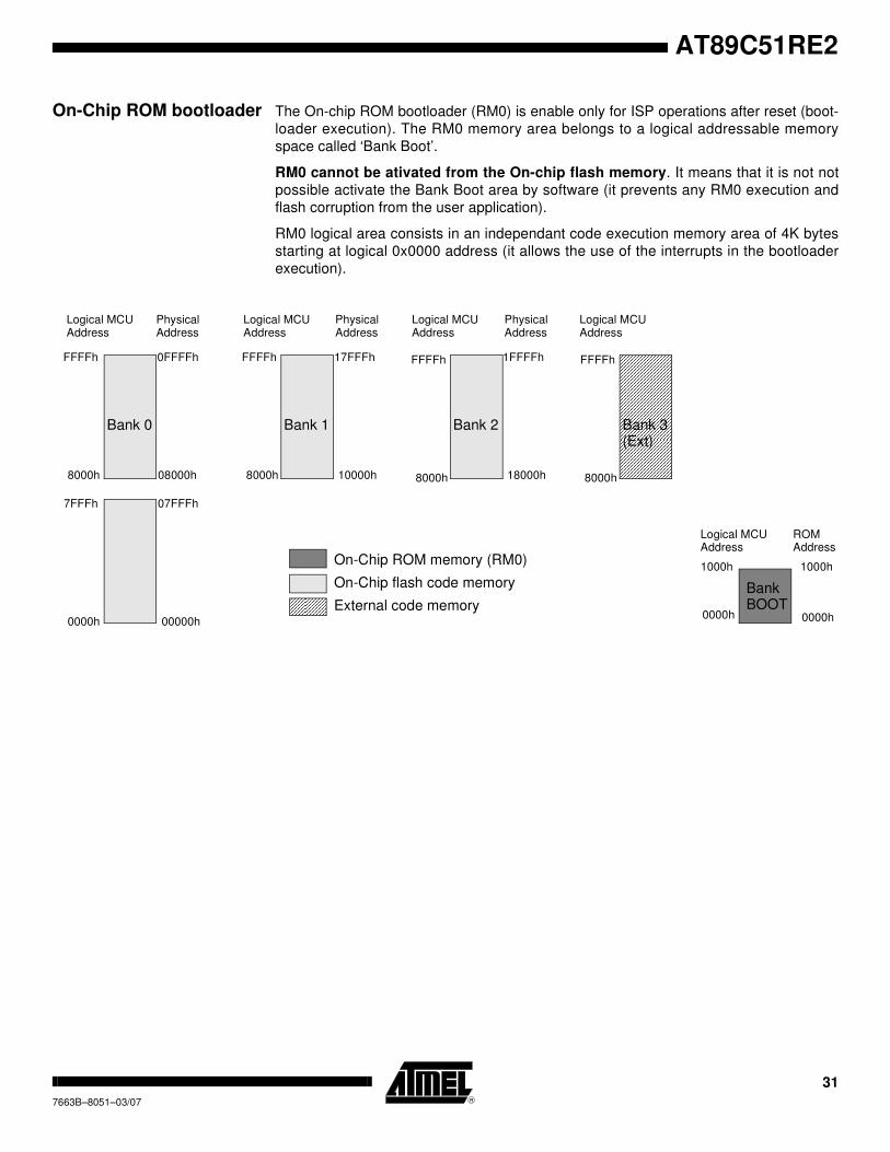
On-Chip ROM bootloader The On-chip ROM bootloader (RM0) is enable only for ISP operations after reset (boot-
loader execution). The RM0 memory area belongs to a logical addressable memory
space called ‘Bank Boot’.
RM0 cannot be ativated from the On-chip flash memory. It means that it is not not
possible activate the Bank Boot area by software (it prevents any RM0 execution and
flash corruption from the user application).
RM0 logical area consists in an independant code execution memory area of 4K bytes
starting at logical 0x0000 address (it allows the use of the interrupts in the bootloader
execution).
0000h
7FFFh
8000h
FFFFh
8000h
FFFFh
8000h
FFFFh
8000h
FFFFh
Bank 0
On-Chip flash code memory
External code memory00000h
07FFFh
08000h
0FFFFh
10000h
17FFFh
18000h
1FFFFh
Logical MCUAddress
PhysicalAddress
Logical MCUAddress
Logical MCUAddress
PhysicalAddress
PhysicalAddress
Logical MCUAddress
Bank 1 Bank 2 Bank 3
Logical MCUAddress
ROMAddress
Bank BOOT
(Ext)
0000h
On-Chip ROM memory (RM0)1000h
0000h
1000h
31
7663B–8051–03/07

Bootprocess The BRV2-0 bits of the FSB (see Table 2 on page 9), the EA pin value upon reset and
the presence of the external hardware conditions, allow to modify the default reset vec-
tor of the AT89C51RE2.
The Hardware conditions (EA = 1, PSEN = 0) during the Reset falling edge force the on-
chip bootloader execution. This allows an application to be built that will normally exe-
cute the end user’s code but can be manually forced into default ISP operation. The
hardware conditions allows to force the enter in ISP mode whatever the configurations
bits.
Figure 3. Boot Reset vector configuration
EA pin Hardware conditions BRV2-0 MCU reset vector
0 X X External Code at address 0x0000
1
YES X RM0 at address 0x0000 (ATMEL Bootloader)
NO
1 1 1 FM0 at address 0x0000 with bank0 mapped
1 1 0 FM0 at address 0xFFFC in Bank 0
1 0 1 FM0 at address 0xFFFC in Bank 1
1 0 0 FM0 at address 0xFFFC in Bank 2
0 1 1 RM0 at address 0x0000 (ATMEL Bootloader)
0 1 0
Reserved
(FM0 at address 0x0000 with bank 0 mapped)0 0 1
0 0 0
32 AT89C51RE27663B–8051–03/07

AT89C51RE2
FM0 Memory Architecture The FM0 flash memory is made up of 5 blocks:
1. The memory array (user space) 128K bytes
2. The Extra Row also called FM0 XAF
3. The Hardware security bits (HSB)
4. The Fuse Configuration Byte (FCB)
5. The column latch
User Space This space is composed of a 128K bytes Flash memory organized in 1024 pages of 128
bytes. It contains the user’s application code. This block can be access in Read/write
mode from FM0 and boot memory area. (When access in write mode from FM0, the
CPU core enter pseudo idle mode).
Extra Row (XRow or XAF) This row is a part of FM0 and has a size of 128 bytes. The extra row (XAF) may contain
information for boot loader usage.This block can be access in Read/write mode from
FM0 and boot memory area. (When access in write mode from FM0, the CPU core enter
pseudo idle mode).
Hardware security Byte (HSB) The Hardware security Byte is a part of FM0 and has a size of 1 byte.
The 8 bits can be read/written by software (from FM0 or RM0) and written by hardware
in parallel mode.
The HSB bits can be written to ‘0’ without any restriction (increase the security level of
the chip), but can be written to ‘1’ only when the corresponding memory area of the lock
bits was full chip erased.
Table 18. Hardware Security Byte (HSB)
7 6 5 4 3 2 1 0
- 1 ELB1 ELBO - FLB2 FLB1 FLB0
Bit
Number
Bit
Mnemonic Description
7 - Unused
6-4 - -
3 - Unused
2-0 FLB2-0FM0 Memory Lock Bits
See Table 21
33
7663B–8051–03/07

Fuse Configuration Byte (FCB) The Fuse configuration byte is a part of FM0.
The 8 bits read/written by software (from FM0 or RM0) and written by hardware in paral-
lel mode.
Table 19. Fuse Configuration Byte (FCB)
7 6 5 4 3 2 1 0
X2 - - - - BRV2 BRV1 BRV0
Bit
Number
Bit
Mnemonic Description
7 X2
X2 Mode
Programmed (‘0’ value) to force X2 mode (6 clocks per instruction) after reset
Unprogrammed (‘1’ value) to force X1 mode, Standard Mode, after reset (Default)
6-3 - Unused
2-0 BRV2-0-
Boot Reset Vector
These bits allow to configure the reset vector of the product according to the
following values:
1 1 1 : Reset at address 0x0000 of FM0 with Bank0 mapped
1 1 0 : Reset at address 0xFFFC of Bank 0
1 0 1 : Reset at address 0xFFFC of Bank 1
1 0 0 : Reset at address 0xFFFC of Bank 2
0 1 1 : Reset at address 0x0000 of RM0 (Internal ROM bootloader execution)
0 1 0 : Reserved for further extension but same as 1 1 1
0 0 1 : Reserved for further extension but same as 1 1 1
0 0 0 : Reserved for further extension but same as 1 1 1
34 AT89C51RE27663B–8051–03/07

AT89C51RE2
Column latches The column latches, also part of FM0, has a size of one page (128 bytes).
The column latches are the entrance buffers of the three previous memory locations
(user array, XROW , Hardware security byte and Fuse Configuration Byte).
This block is writen only from FM0, RM0.
Cross Memory Access Description overview
The FM0 memory can be programmed from RM0 without entering idle mode.
Programming FM0 from FM0 makes the CPU core entering “pseudo idle” mode.
In the pseudo idle mode, the code execution is halted, the peripherals are still running (
like standard idle mode) but all interrupt are delayed to the end of this mode. There are
fours ways of exiting pseudo idle mode:
• At the end of the regular flash programming operation
• Reset the chip by external reset
• Reset the chip by hardware watchdog
• Reset the chip by PCA watchdog
Programming FM0 from external memory code (EA=0 or EA=1,with Bank3 active) is
impossible.
If a reset occurs during flash programming the target page could be uncompletly erased
or programmed, but any other memory location (FM0, RAM, XRAM) remain unchanged.
The Table 20 shows all software flash access allowed.
Table 20. Cross Memory Access
Co
de
exe
cu
tin
g f
rom
ActionFM0
(user Flash)
RM0
(boot ROM)
FM0
(user Flash)
Read ok Denied
Load column latch ok N.A.
Write ok ( pseudo idle mode ) N.A.
RM0
(boot ROM)
Read ok ok
Load column latch ok N.A.
Write ok N.A.
External memory
EA = 0
or
EA=1, Bank3
Read (1) Denied
Load column latch Denied N.A.
Write Denied N.A.
1. Depends of general lock bits configuration
N.A. Not applicable
35
7663B–8051–03/07

Access and Operations Descriptions
FM0 FLASH Registers
The CPU interfaces to the flash memory through the FCON register, AUXR1 register
and FSTA register.
These registers are used to map the columns latche, HSB, FCB and extra row in the
working data or code space.
BMSEL Register
Table 21. BMSEL Register
BMSEL Register (S:92h)
Bank Memory Select
Reset Value= 0000 0YYYb (where YYY depends on BRV2:0 value in Fuse Configura-
tion Byte)
7 6 5 4 3 2 1 0
MBO2 MBO1 MBO0 FBS2 FBS1 FBS0
Bit
Number
Bit
Mnemonic Description
7-5 MBO2:0
Memory Bank Operation
These bits select the target memory bank for flash write or read operation. These
bits allows to read or write the on-chip flash memory from one upper 32K bytes to
another one.
0 X X :The on-chip flash operation target banked is the same as FBS2:0
1 0 0 : The target memory bank is forced to Bank0
1 0 1 : The target memory bank is forced to Bank1
1 1 0 : The target memory bank is forced to Bank2
1 1 1 : The target memory bank is forced to Bank3 (optionnal External bank)
4-3 Reserved
2-0 FBS2:0
Fetch Bank Selection
These bits select the upper 32K bytes execution bank:
FBS1:0 can be read/write by software.
FBS2 is readonly by software (the Boot bank can not be mapped from FM0)
0 0 0 Bank0
0 0 1 Bank1
0 1 0 Bank2
0 1 1 Bank3 (optionnal external bank)
1 X X Boot Bank (Read only)
Upon reset FBS2:0 is initialiazed according to BRV2:0 configuration bits in FCB.
36 AT89C51RE27663B–8051–03/07

AT89C51RE2
FCON Register
Table 22. FCON Register
FCON Register (S:D1h)
Flash Control Register
Reset Value= 0000 0000b
7 6 5 4 3 2 1 0
FPL3 FPL2 FPL1 FPL0 FPS FMOD2 FMOD1 FMOD0
Bit
Number
Bit
Mnemonic Description
7-4 FPL3:0
Programming Launch Command Bits
Write 5Xh followed by AXh to launch the programming according to FMOD2:0.
(see Table 25.)
3 FPS
Flash Map Program Space
When this bit is set:
The MOVX @DPTR, A instruction writes in the columns latches space
When this bit is cleared:
The MOVX @DPTR, A instruction writes in the regular XDATA memory space
2-0 FMOD2:0
Flash Mode
These bits allow to select the target memory area and operation on FM0
See Table 24.
37
7663B–8051–03/07

FSTA Register
Table 23. FSTA Register
FSTA Register (S:D3h)
Flash Status Register
Reset Value= ‘R’xxx x000b
Where ‘R’ depends on the reset conditions: If RM0 is executed after Reset R=1, if FM0
is executed after reset R=0
7 6 5 4 3 2 1 0
FMR - - - - FSE FLOAD FBUSY
Bit
Number
Bit
Mnemonic Description
7 FMR
Flash Movc Redirection
When code is executed from RM0 (and only RM0), this bit allow the MOVC
instruction to be redirected to FM0.
Clear this bit to allow MOVC instruction to read FM0
Set this bit to allow MOVC instruction to read RM0
This bit can be written only from RM0 (on-chip ROM bootloader execution).
6-3 - unused
2 FSE
Flash sequence error
Set by hardware when the flash activation sequence(MOV FCON 5X and MOV
FCON AX )is not correct (See Error Report Section)
Clear by software or clear by hardware if the last activation sequence was
correct (previous error is canceled)
1 FLOAD
Flash Columns latch loaded
Set by hardware when the first data is loaded in the column latches.
Clear by hardware when the activation sequence succeded (flash write sucess,
or reset column latch success)
0 FBUSY
Flash Busy
Set by hardware when programming is in progress.
Clear by hardware when programming is done.
Can not be changed by software.
38 AT89C51RE27663B–8051–03/07

AT89C51RE2
Mapping of the Memory Space
By default, the user space is accessed by MOVC A, @A+DPTR instruction for read
only. Setting FPS bit in FCON register takes precedence on the EXTRAM bit in AUXR
register.
The other memory spaces (user, extra row, hardware security) are made accessible in
the code segment by programming bits FMOD2:0 in FCON register in accordance with
Table 24. A MOVC instruction is then used for reading these spaces.
Thanks to the columns latches access , it is possible to write FM0 array, HSB and extra
row blocks. The column latches space is made accessible by setting the FPS bit in
FCON register. Writing is possible from 0000h to FFFFh, address bits 6 to 0 are used to
select an address within a page while bits 14 to 7 are used to select the programming
address of the page.
Table 24. .FM0 blocks select bits
FMOD2 FMOD1 FMOD0 Adressable Space
0 0 0 FM0 array(0000h-FFFFh)
0 0 1 Extra Row(00h-80h)
0 1 0 Erase FM0
0 1 1 Colum latches reset
1 0 0 HSB
1 0 1 FCB
1 1 0Reserved
1 1 1
39
7663B–8051–03/07

Launching flash commands (activation sequence)
FPL3:0 bits in FCON register are used to secure the launch of programming. A specific
sequence must be written in these bits to unlock the write protection and to launch the
operation. This sequence is 5xh followed by Axh. Table 25 summarizes the memory
spaces to program according to FMOD2:0 bits.
Table 25. FM0 Programming Sequences
Note: 1. The sequence 5xh and Axh must be executed without instructions between them oth-
erwise the programming is not executed (see flash status register).
2. The sequence 5xh and Axh can be executed with the differents FMOD0, FMOD1 val-
ues, the last FMOD1:0 value latches the destination target.
3. When the FMOD2 bit is set (coreesponding to the serial number field code) no write
operation can be performed.
4. Only the bits coresponding to the previously “full erase” memory space can be written
to one.
Write to FCON
OperationFPL3:0 FPS FMOD2 FMOD1 FMOD0
FM05 X 0 0 0 No action
A X 0 0 0 Write the column latches in FM0
XAF
FM0
5 X 0 0 1 No action
A X 0 0 1Write the column latches in FM0
extra row space
Erase FM0 5 X 0 1 0 No action
A X 0 1 0 Full erase FM0 memory area
Reset
FM0
Column
Latches
5 X 0 1 1 No action
A X 0 1 1 Reset the FM0 column latches
HSB
5 X 1 0 0 No action
A X 1 0 0Write the hardware Security byte
(HSB) See (4)
FCB
5 X 1 0 1 No action
A X 1 0 1Write the Fuse Configuration Byte
(FCB)
Reserved5 X 1 1 0
No actionA X 1 1 0
Reserved5 X 1 1 1
A X 1 1 1
40 AT89C51RE27663B–8051–03/07

AT89C51RE2
Loading the Column Latches
Any number of data from 0 byte to 128 bytes can be loaded in the column latches. The
data written in the column latches can be written in a none consecutive order. The
DPTR allows to select the address of the byte to load in the column latches.
The page address to be written (target page in FM0) is given by the last address loaded
in the column latches and when this page belongs to the upper 32K bytes of the logical
addressable MCU space, the target memory bank selection is performed upon the
MBO2:0 value during the last address loaded.
When 0 byte is loaded in the column latches the activation sequence ( 5xh, Axh in
FCON) does not launch any operations. The FSE bit in FSTA register is set.
When a current flash write operation is on-going (FBUSY is set), it is impossible to load
the columns latches before the end of flash programming process (the write operation in
the columns latches is not performed, and the previous columns latches content is not
overwritten).
When programming is launched, an automatic erase of the entire memory page is first
performed, then programming is effectively done. Thus no page or block erase is
needed and only the loaded data are programmed in the corresponding page. The
unloaded data of the target memory page are programmed at 0xFF value (automatic
page erase value).
The following procedure is used to load the column latches and is summarized in
Figure 4:
• Disable interrupt and map the column latch space by setting FPS bit.
• Select the target memory bank (for page address larger than 32K)
• Map the column latch
• Reset the column latch
• Load the DPTR with the address to write.
• Load Accumulator register with the data to write.
• Execute the MOVX @DPTR, A instruction, and only this one (no MOVX @Ri, A).
• If needed loop the last three instructions until the page is completely loaded.
• Unmap the column latch if needed (it can be left mapped) and Enable Interrupt
41
7663B–8051–03/07

Figure 4. Column Latches Loading Procedure
Note: The last page address used when loading the column latch is the one used to select the
page programming address.
Note: The value of MB02:0 during the last load gives the upper 32K bytes bank target
selection.
Note: The execution of this sequence when BUSY flag is set leads to the no-execution of the
write in the column latches (the previous loaded data remains unchanged).
Writting the Flash Spaces
User The following procedure is used to program the User space and is summarized in
Figure 5:
• Load up to one page of data in the column latches from address 0000h to FFFFh (
see Figure 4.).
• Disable the interrupts.
• Launch the programming by writing the data sequence 50h followed by A0h in
FCON register.
The end of the programming indicated by the FBUSY flag cleared.
Column Latches
Loading
Data LoadDPTR= Address
ACC= DataExec: MOVX @DPTR, A
Last Byte
to load ?
Data memory MappingFCON = 00h (FPS = 0)
Save & Disable ITEA= 0
Restore IT and default taget memory bank
Select target bankMB2:0=YY
Column Latches ResetFCON= 53h (FPS=0)FCON= ABh (FPS=1)
42 AT89C51RE27663B–8051–03/07

AT89C51RE2
• Enable the interrupts.
Extra Row The following procedure is used to program the Extra Row space and is summarized in
Figure 5:
• Load data in the column latches from address FF80h to FFFFh.
• Disable the interrupts.
• Launch the programming by writing the data sequence 51h followed by A1h in
FCON register.
The end of the programming indicated by the FBUSY flag cleared.
• Enable the interrupts.
Figure 5. Flash and Extra row Programming Procedure
Hardware Security Byte (HSB) The following procedure is used to program the Hardware Security Byte spaceand is summarized in Figure 6:
• Set FPS and map Hardware byte (FCON = 0x0C)
• Save and disable the interrupts.
• Load DPTR at address 0000h
• Load Accumulator register with the data to load.
Flash
Programming
Save & Disable ITEA= 0
Launch ProgrammingFCON= 50hFCON= A0h
End ProgrammingRestore IT
Column Latches Loadingsee Figure 4
FBusy
Cleared?
Clear ModeFCON = 00h
XROW
Programming
Save & Disable ITEA= 0
Launch ProgrammingFCON= 51hFCON= A1h
End ProgrammingRestore IT
Column Latches Loadingsee Figure 4
FBusy
Cleared?
Clear ModeFCON = 00h
43
7663B–8051–03/07

• Execute the MOVX @DPTR, A instruction.
• Launch the programming by writing the data sequence 54h followed by A4h in
FCON register.
The end of the programming indicated by the FBusy flag cleared.
• Restore the interrupts
.
Figure 6. Hardware Security Byte Programming Procedure
Fuse Configuration Byte (FCB) The following procedure is used to program the Fuse Configuration Byte spaceand is summarized in Figure 7:
• Set FPS and map FCB (FCON = 0x0D)
• Save and disable the interrupts.
• Load DPTR at address 0000h
• Load Accumulator register with the data to load.
• Execute the MOVX @DPTR, A instruction.
HSB
Programming
Launch ProgrammingFCON= 54hFCON= A4h
End ProgrammingRestoreIT
FBusy
Cleared?
Clear ModeFCON = 00h
Data LoadDPTR= 00hACC= Data
Exec: MOVX @DPTR, A
FCON = 0Ch
Save & Disable ITEA= 0
44 AT89C51RE27663B–8051–03/07

AT89C51RE2
• Launch the programming by writing the data sequence 55h followed by A5h in
FCON register.
The end of the programming indicated by the FBusy flag cleared.
• Restore the interrupts
.
Figure 7. Fuse Configuration Byte Programming Procedure
Reset of columns latches space
No automatic reset of the columns latches is performed after a successfull flashwrite process. Resetting the columns latches during a flash write process ismandatory. User shall implement a reset of the column latch before each col-umn latch load sequence.
FCB
Programming
Launch ProgrammingFCON= 55hFCON= A5h
End ProgrammingRestoreIT
FBusy
Cleared?
Clear ModeFCON = 00h
Data LoadDPTR= 00hACC= Data
Exec: MOVX @DPTR, A
FCON = 0Dh
Save & Disable ITEA= 0
45
7663B–8051–03/07

In addition, the user application can reset the columns latches space manually.The following procedure is used to reset the columns latches space
Launch the programming by writing the data sequence 53h followed by A3h inFCON register (from FM0 and RM0).
46 AT89C51RE27663B–8051–03/07

AT89C51RE2
Errors Report / Miscelaneous states
Flash Busy flag The FBUSY flag indicates on-going flash write operation.
The busy flag is set by hardware, the hardware clears this flag after the end of the pro-
gramming operation.
Flash Programming Sequence
Error
When a wrong sequence is detected the FSE in FSTA is set.
The following events are considered as not correct activation sequence:
- The two “MOV FCON,5x and MOV FCON, Ax” were not consecutive, or the second
intruction differs from “MOV FCON Ax” (for example, an interrupt occurs during the
sequence).
- The sequence(write flash or reset column latches) occured with no data loaded in the
column latches
The FSE bit can be cleared:
- By software
- By hardware when a correct programming sequence sequence occurs.
Note: When a good sequence occurs just after an incorrect sequence, the previous error
is lost. The user software application should take care to check the FSE bit before initiat-
ing a new sequence.
Power Down Mode Request
In Power Down mode, the on-chip flash memory is deselected (to reduce power con-
sumption), this leads to the lost of the columns latches content.
In this case, if columns latches were previously loaded they are reseted: FLOAD bit in
FSTA register should be reseted after power down mode.
If a power down mode is requested during flash programming (FBUSY=1), all power
down sequence instructions should be ignored until the end of flash process.
47
7663B–8051–03/07

Reading the Flash Spaces
User The following procedure is used to read the User space:
• Read one byte in Accumulator by executing MOVC A,@A+DPTR
Note: FCON is supposed to be reset when not needed.
Depending of the MBO2:0 bits, the MOVC A,@A+DPTR can address a specific upper
32K bytes bank. It allows to read the 32K bytes upper On-chip flash memory from one
bank to another one.
When read from the bootloader area, the user memory shall be mapped before any read
access by setting the FMR bit of the FSTA register.
By default, when the bootloader is entered by hardware conditions, the ROM area is
mapped for MOVC A,@A+DPTR operations. It is necessary to remap the user memory
before each read access.
Extra Row (XAF) The following procedure is used to read the Extra Row space and is summarized in
Figure 8:
• Map the Extra Row space by writing 01h in FCON register.
• Read one byte in Accumulator by executing MOVC A,@A+DPTR with A= 0 &
DPTR= 0000h to 007Fh.
• Clear FCON to unmap the Extra Row.
Figure 8. XAF Reading Procedure
Hardware Security Byte The following procedure is used to read the Hardware Security space and issummarized in Figure 9:
• Map the Hardware Security space by writing 04h in FCON register.
• Read the byte in Accumulator by executing MOVC A,@A+DPTR with A= 0 &
DPTR= 0000h.
• Clear FCON to unmap the Hardware Security Byte.
XRAW Reading
Data ReadDPTR= @ ( 00h up to 7Fh
ACC= 0Exec: MOVC A, @A+DPTR
XRAW MappingFCON = 01h
XRAW UnmappingFCON = 00h (FPS = 0)
48 AT89C51RE27663B–8051–03/07

AT89C51RE2
Figure 9. HSB Reading Procedure
Fuse ConfigurationByte The following procedure is used to read the Fuse Configuration byte and is sum-marized in Figure 9:
• Map the FCB by writing 05h in FCON register.
• Read the byte in Accumulator by executing MOVC A,@A+DPTR with A= 0 &
DPTR= 0000h.
• Clear FCON to unmap the Hardware Security Byte.
HSB Reading Procedure
HSB Reading
Data ReadDPTR= 0000h
ACC= 00hExec: MOVC A, @A+DPTR
HSB MappingFCON = 04h
HSB UnmappingFCON = 00h (FPS = 0)
FCB Reading
Data ReadDPTR= 0000h
ACC= 00hExec: MOVC A, @A+DPTR
FCB MappingFCON = 05h
HSB UnmappingFCON = 00h (FPS = 0)
49
7663B–8051–03/07

Operation Cross Memory Access
Space addressable in read and write are:
• RAM
• ERAM (Expanded RAM access by movx)
• XRAM (eXternal RAM)
• FM0 ( user flash )
• Hardware byte
• XROW FM0
• Boot RM0
• Flash Column latch
The table below provide the different kind of memory which can be accessed from differ-
ent code location.
Table 26. Cross Memory Access
Action RAM
XRAM
ERAM boot RM0 FM0 HSB FCB XAF FM0
boot RM0Read ok ok ok ok ok ok ok
Write ok ok - ok (RWW) ok (RWW) ok (RWW) ok (RWW)
FM0Read ok ok - ok ok ok ok
Write ok ok - ok (idle) ok ok ok
External
memory
EA = 0
or BANK3
Read ok ok - - - - -
Write ok ok - - - - -
50 AT89C51RE27663B–8051–03/07

AT89C51RE2
Sharing Instructions
Table 27. Instructions shared
Note: by cl : using Column Latch
Table 28. Write MOVX @DPTR,A
Table 29. MOVC A, @A+DPTR executed from External code EA=0
Table 30. MOVC A, @A+DPTR executed from External code EA=1, PC>=0x8000,
FBS=Bank3
Action RAM XRAM RM0 CL FM0 FM0 HSB XAF FM0
Read MOVMOVX
A,@DPTR
MOVC A,
@A+DPTR-
MOVC A,
@A+DPTR
MOVC A,
@A+DPTR
MOVC A,
@A+DPTR
Write MOVMOVX
@DPTR,A-
MOVX
@DPTR,A
by CL
FM0
by CL
FM0
by CL
FM0
FPS of
FCCON EA
XRAM
ERAM CL FM0
0 X winner
11 winner
0 winner
FMOD2:0
FBS
(Fetch)
MBO
(Target)MOVC A,@A+DPTR
X X X Read External Code
FMOD2:0
MBO
(Target)DPTR MOVC A,@A+DPTR
X X < 0x8000
Depends on FLB2:0
Can Returns Random value, for secured part.
X >= 0x8000 External code read
51
7663B–8051–03/07

Flash Protection from Parallel Programming
The three lock bits in Hardware Security Byte (see "In-System Programming" section)
are programmed according to Table 21 provide different level of protection for the on-
chip flash memory FM0.
They are set by default to level 4
Table 31. Program Lock Bit FLB2-0
Program Lock bits
U: unprogrammed
P: programmed
WARNING: Security level 2 and 3 should only be programmed after verification.
Program Lock Bits
Protection Description
Security
levelFLB0 FLB1 FLB2
1 U U U No program lock features enabled.
2 P U U
MOVC instruction executed from external program memory are
disabled from fetching code bytes from internal memory, EA is sampled
and latched on reset, and further parallel programming of the Flash is
disabled.
ISP allows only flash verification (no write operations are allowed) but
IAP from internal code still allowed.
3 U P USame as 2, also verify through parallel programming interface is
disabled and ISP read operation not allowed.
4 U U PSame as 3, also external execution is disabled (external bank not
accessible)
52 AT89C51RE27663B–8051–03/07

Bootloader Architecture
Introduction The bootloader manages a communication between a host platform running an ISP tool
and a AT89C51RE2 target.
The bootloader implemented in AT89C51RE2 is designed to reside in the dedicated
ROM bank. This memory area can only be executed (fetched) when the processor
enters the boot process.
The implementation of the bootloader is based on standard set of libraries including
INTEL hex based protocol, standard communication links and ATMEL ISP command
set.
Figure 3. Bootloader Functional Description
On the above diagram, the on-chip bootloader processes are:
• ISP Communication Management
The purpose of this process is to manage the communication and its protocol between
the on-chip bootloader and a external device. The on-chip ROM implement a serial pro-
tocol (see section Bootloader Protocol). This process translate serial communication
frame (UART) into Flash memory acess (read, write, erase ...).
• Memory Management
This process manages low level access to Flash memory (performs read and write
access).
ISP CommunicationManagementSpecific Protocol
Communication
Management
Memory
Exernal Host with
Memory
Bootloader
36 AT89C51RE27663B–8051–03/07

AT89C51RE2
Bootloader Description
Entry points After reset only one bootloader entry point is possible. This entry point stands at
address 0x0000 of the boot ROM memory. This entry point executes the boot process of
the bootloader.
The bootloader entry point can be selected through two processes :
At reset, if the hardware conditions are applied, the bootloader entry point is accessed
and executed.
At reset, if the hardware conditions are not set and the BRV2-0 is programmed ‘011’, the
bootloader entry point is accessed and the bootprocess is started.
Boot Process Description The boot process consists in three main operations :
• The hardware boot process request detection
• The communication link detection (Uart or OCD)
• The start-up of the bootloader
Hardware boot process request
detection
The hardware boot process request is detected when the hardware conditions (under
reset, EA=1 and PSEN=0) are received by the processor or when no hardware condition
is applied and the BRV2:0 is configured ‘011’.
Communication link detection Two interfaces are available for ISP :
• UART0
• OCD UART
Ha
rdw
are
B
oo
t P
roc
es
s
RESET
BRV=’011’
PC = RM0 @0x0000h
Communication link
Start Bootloader
Start Application
BRV=’100’EA=1
PSEN=0
Yes
No
Yes
No
detector / initialiser
Yes
NoBRV=’101’
Yes
NoBRV=’110’
Yes
No
PC
= F
M0
Ba
nk2
@0
xF
FF
Ch
PC
= F
M0
Ba
nk1
@0
xF
FF
Ch
PC
= F
M0
Ba
nk0
@0
xF
FF
Ch
PC
= F
M0
Ba
nk0
@0
xF
FF
Ch
37
7663B–8051–03/07

The communication link detection is done by a circular polling on all the interfaces. On
AT89C51RE2, the ISP interfaces are all based on simple UART mechanisms (Rx, Tx).
The Rx line default state is ‘1’ when no communication is in progress. A transition from
‘1’ to ‘0’ on the Rx line indicates a start of frame.
Once one of the interface detects a starts of frame (‘0’) on its Rx line, the interface is
selected and configuration of the communication link starts.
Figure 4. Communication link Detection
Notes: 1. SF : Start of Frame (‘0’ = detected ; ‘1’ = not detected)
2. In AT89C51RE2 implementation, Interface 1 refers to UART0 and Interface 2 refers
to the OCD UART interface.
Yes
No
Interface 1
SF = 0
Yes
No
Interface 2
SF = 0
DetectionStart
Interface 1
Initialisation
Interface 2
Initialisation
Start Bootloader
38 AT89C51RE27663B–8051–03/07

AT89C51RE2
ISP Protocol Description
Physical Layer The UART used to transmit information has the following configuration:
• Character: 8-bit data
• Parity: none
• Stop: 1 bit
• Flow control: none
• Baud rate: autobaud is performed by the bootloader to compute the baud rate
chosen by the host.
Frame Description The Serial Protocol is based on the Intel Extended Hex-type records.
Intel Hex records consist of ASCII characters used to represent hexadecimal values and
are summarized below.
Table 24. Intel Hex Type Frame
• Record Mark:
– Record Mark is the start of frame. This field must contain ’:’.
• Record length:
– Record length specifies the number of Bytes of information or data which
follows the Record Type field of the record.
• Load Offset:
– Load Offset specifies the 16-bit starting load offset of the data Bytes,
therefore this field is used only for
– Data Program Record.
• Record Type:
– Record Type specifies the command type. This field is used to interpret the
remaining information within the frame.
• Data/Info:
– Data/Info is a variable length field. It consists of zero or more Bytes encoded
as pairs of hexadecimal digits. The meaning of data depends on the Record
Type.
• Checksum:
– Checksum is the two’s complement of the 8-bit Bytes that result from
converting each pair of ASCII hexadecimal digits to one Byte of binary, thus
including all field from the Record Length field to the last Byte of the
Data/Info field. Therefore, the sum of all the ASCII pairs in a record after
converting to binary, including all field from the Record Length field to the
Checksum field, is zero.
Record Mark ‘:’ Record length Load Offset Record Type Data or Info Checksum
1 byte 1 byte 2 bytes 1 bytes n byte 1 byte
39
7663B–8051–03/07

Protocol
Overview An initialization step must be performed after each Reset. After microcontroller reset,
the boot loader wai ts for an autobaud sequence (see Sect ion “Autobaud
Performances”).
When the communication is initialized the protocol depends on the record type issued
by the host.
Communication Initialization The host initiates the communication by sending a ’U’ character to help the bootloader
to compute the baudrate (autobaud).
Figure 5. Initialization
Autobaud Performances The bootloader supportsa wide range of baud rates. It is also adaptable to a wide range
of oscillator frequencies. This is accomplished by measuring the bit-time of a single bit in
a received character. This information is then used to program the baud rate in terms of
timer counts based on the oscillator frequency. Table 30 shows the autobaud
capabilities.
Command Data Stream Protocol
All commands are sent using the same flow. To increase performance, the echo has
been removed from the bootloader response.
Figure 6. Command Flow
Host Bootloader
"U"Performs Autobaud
Init Communication
If (not received "U") "U"
Communication OpenedElse
Sends Back ‘U’ Character
Bootloader
":"Sends first character of theFrame
If (not received ":")
Sends frame (made of 2 ASCII Gets frame, and sends back echofor each received Byte
Host
Else":"
Sends echo and start reception
characters per Byte)Echo analysis
40 AT89C51RE27663B–8051–03/07

AT89C51RE2
Each command flow may end with:
• “X” : If checksum error
• “L” : If read security is set
• “P”: If program security is set
• “.”: If command ok
• byte + “.” : read byte ok
41
7663B–8051–03/07

Reading/Blank checking memory
To start the reading or blank checking operation,
Requests from Host
Answers from Bootloader The boot loader can answer to a read command with:
• ‘Address = data ‘ & ‘CR’ & ’LF’ the number of data by line depends of the bootloader.
• ‘X’ & ‘CR’ & ‘LF’ if the checksum is wrong
• ‘L’ & ‘CR’ & ‘LF’ if the Security is set
The bootloader answers to blank check command:
• ‘.’ & ‘CR’ & ’LF’ when the blank check is ok
• ‘First Address wrong’ ‘CR’ & ‘LF’ when the blank check is fail
• ‘X’ & ‘CR’ & ‘LF’ if the checksum is wrong
• ‘L’ & ‘CR’ & ‘LF’ if the Security is set
Changing memory/page To change the memory selected and/or the page, the Host can send two commands.
• Select New Page to keep the same memory.
• Select Memory to change the Memory and page
Requests from Host
Answers from Bootloader The boot loader can answer to a read command with:
• ‘. ‘ & ‘CR’ & ’LF’ if the command is done
• ‘X’ & ‘CR’ & ‘LF’ if the checksum is wrong
Command
Record
Type
Record
Length Offset Data[0] Data[1] Data[2] Data[3] Data[4]
Read selected memory04h 05h 0000h Start Address End Address
00h
Blank Check selected memory 01h
Command
Record
Type
Record
Length Offset Data[0] Data[1]
Select New Page 02h 02hstart
address
Page (4
bits) + 0h00h
Select Memory 04h 02h 0000hMemory
spacePage
42 AT89C51RE27663B–8051–03/07

AT89C51RE2
Programming/Erasing memory
Requests from Host
Answers from Bootloader The boot loader answers with:
• ‘.’ & ‘CR’ & ’LF’ when the data are programmed
• ‘X’ & ‘CR’ & ‘LF’ if the checksum is wrong
• ‘P’ & ‘CR’ & ‘LF’ if the Security is set
Starting application The application can only be started by a Watchdog reset.
No answer is returned by the bootloader.
Requests from Host
Command
Record
Type
Record
Length Offset Data[0] Data[1] Data[2] Data[3] Data[4]
Program selected memory 00h nb of datastart
addressx x x x x
Erase selected memory 04h 05h 0000h 00h FFh 00h 00h 02h
Command
Record
Type
Record
Length Offset
Start application with watchdog 01h 00h 0000h
43
7663B–8051–03/07

ISP Commands description
Select Memory Space The ‘Select Memory Space’ command allows to route all read, write commands to a
selected area. For each area (Family) a code is defined. This code corresponds to the
memory area encoded value in the INTEL HEX frame .
The area supported and there coding are listed in the table below.
Table 25. Memory Families & coding
The Bootloader information and the signature areas are read only. The value in the cod-
ing column is the value to report in the corresponding protocol field.
Note: * the coding number doesn’t include any information on the authorized address range of
the family. A summary of these addresses is available in appendix (See “Address Map-
ping” on page 50.)
Memory/Information Family coding* name
FLASH 0 MEM_FLASH
SECURITY 7 MEM_PROTECT
CONFIGURATION 8 MEM_CONF
BOOTLOADER 3 MEM_BOOT
SIGNATURE 6 MEM_SIGNATURE
44 AT89C51RE27663B–8051–03/07

AT89C51RE2
Select Page The ‘Select Page’ command allows to define a page number in the selected area. A page
is defined as a 64K linear memory space (According to the INTEL HEX format). It
doesn’t corresponds to a physical bank from the processor.
The following table summarizes the memory spaces for which the select page command
can be applied.
Table 26. Memory space & Select page
Table 27.
Memory/Information Family Comments/Restriction
FLASH page 0 (0->64K) and 1(64k->128k)
available
45
7663B–8051–03/07

Write commands The following table summarizes the memory spaces for which the write command can
be applied.
Table 28. Memory space & Select page
In case of write command to other area, nothing is done.
The bootloader returns a Write protection (‘P’) if the SECURITY do not allow any write
operation from the bootloader.
FLASH The program/data Flash memory area can be programmed by the bootloader by data
pages of up to 128bytes.
If the Flash memory security level is at least ‘2’ (FLB2:0 = ‘110’), no write operation can
be performed through the bootloader.
Table 29. Flash Write Autorisation Summary
CONFIGURATION The FCB configuration byte can always be written, whatever are the security levels.
SECURITY The Security byte can always be written with a value that enables a protection higher
than the previous one.
If attempting to write a lower security, no action is performed and the bootloader returns
a protection error code (‘P’)
Table 31. Security Write Autorisation Summary
Memory/Information Family Comments/Restriction
FLASH need security level check
SECURITY only a higher level can be writen
CONFIGURATION
Table 30.
Command
Security level (HSB)
FLB2:0
111 110 101 011
Write Allowed Forbidden Forbidden Forbidden
write from
FLB2:0
Security level (HSB)
to FLB2:0
111 110 101 011
111 Allowed Allowed Allowed Allowed
110 Forbidden Allowed Allowed Allowed
101 Forbidden Forbidden Allowed Allowed
011 Forbidden Forbidden Forbidden Allowed
46 AT89C51RE27663B–8051–03/07

AT89C51RE2
Erasing commands The erasing command is supported by the following areas :
Table 32. Memory space & Erase
Nothing is done on the other areas.
FLASH The erasing command on the Flash memory:
• erases the four physical flash memory banks (from address 0000h to 1FFFFh).
• the HSB (Hardware Security Byte) is set at NO_PROTECTION :
– FLB2.0 = ‘111’
Memory/Information Family Comments/Restriction
FLASH need security level check
47
7663B–8051–03/07

Blank Checking commands The blank checking command is supported by the following areas
Table 33. Memory space & Erase
Nothing is done on the other areas.
The first not erased address is returned if the blank check is failed.
FLASH The blank checking command on the Flash memory can be done from address 0000h to
1FFFFh.
The blanck check operation is only possible if the HSB (Hardware Security Byte) has a
security level lower than or equal to ‘2’ (FLB2.0 = ‘110’)
Table 34. Flash Blank check Autorisation Summary
–
Memory/Information Family Comments/Restriction
FLASH need security level check
Command
Security level (HSB)
FLB2:0
111 110 101 011
Blank Check Allowed Allowed Forbidden Forbidden
48 AT89C51RE27663B–8051–03/07

AT89C51RE2
Reading commands The reading command is supported by the following areas :
Table 35. Memory space & Select page
FLASH The reading command on the Flash memory can be done from address 000h to
1FFFFh. The read operation is only possible if the HSB (Hardware Security Byte) has a
security level lower than or equal to ‘2’ (FLB2.0 = ‘110’)
Table 36. Flash Read Autorisation Summary
CONFIGURATION The CONFIGURATION family can always be read.
SECURITY The SECURITY family can always be read.
BOOTLOADER All the field from the BOOTLOARED family can be read from the bootloader. Each boot-
loader information shall be read unitary. Accesses must be done byte per byte
according to the address definition
SIGNATURE All the field from the SIGNATURE family can be read from the bootloader. Each signa-
ture information shall be read unitary. Accesses must be done byte per byte according
to the address definition
Memory/Information Family Comments/Restriction
FLASH need security level check
SECURITY
CONFIGURATION
BOOTLOADER
SIGNATURE
Command
Security level (HSB)
FLB2:0
111 110 101 011
Read Allowed Allowed Forbidden Forbidden
49
7663B–8051–03/07

Start Application The start application command is used to quit the bootloader and start the application
loaded.
The start application is performed by a watchdog reset.
The best way to start the application from a user defined entry point is to configure the
FCB (Fuse Configuration Byte) before launching the watchdog. Then, depending on the
configuration of the BRV2:0 field, the hardware boots from the selected memory area.
ISP Command summary
UART Protocol frames
Address Mapping
Table 38. Memory Families, Addresses & Coding
Table 37. Summary of frames from Host
Command
Record
Type
Record
Length Offset Data[0] Data[1] Data[2] Data[3] Data[4]
Program selected memory 00h nb of datastart
addressx x x x x
Start application with watchdog 01h 00h 0000h x x x x x
Select New Page 02h 02hstart
address
Page (4
bits) + 0h00h x x x
Select Memory
04h
02h 0000hMemory
spacePage x x x
Read selected memory
05h 0000hStart Address End Address
00h
Blank Check selected memory 01h
Erase Selected memory 00h FFh 00h 00h 02h
Table 39.
Memory/Parameter coding Address Page number
Memory/Information
Family
FLASH 0 0 up to 0x1FFFF 0 up to 1 FLASH
HSB 7 0 0 SECURITY
FCB 8 0 0 CONFIGURATION
Bootloader revision
3
00h
0 BOOTLOADERBoot id1 01h
Boot id2 02h
Manuf. code
6
30h
0 SIGNATUREFamily code 31h
Product name 60h
Product rev 61h
50 AT89C51RE27663B–8051–03/07

AT89C51RE2
Attempting an access with any other ‘coding’, ‘page number’ or ‘Address’ results in no
action and no answer from the bootloader.
51
7663B–8051–03/07

Timers/Counters The AT89C51RE2 implements two general-purpose, 16-bit Timers/Counters. Such are
identified as Timer 0 and Timer 1, and can be independently configured to operate in a
variety of modes as a Timer or an event Counter. When operating as a Timer, the
Timer/Counter runs for a programmed length of time, then issues an interrupt request.
When operating as a Counter, the Timer/Counter counts negative transitions on an
external pin. After a preset number of counts, the Counter issues an interrupt request.
The various operating modes of each Timer/Counter are described in the following
sections.
Timer/Counter Operations
A basic operation is Timer registers THx and TLx (x = 0, 1) connected in cascade to
form a 16-bit Timer. Setting the run control bit (TRx) in TCON register (see Figure 40)
turns the Timer on by allowing the selected input to increment TLx. When TLx overflows
it increments THx; when THx overflows it sets the Timer overflow flag (TFx) in TCON
register. Setting the TRx does not clear the THx and TLx Timer registers. Timer regis-
ters can be accessed to obtain the current count or to enter preset values. They can be
read at any time but TRx bit must be cleared to preset their values, otherwise the behav-
ior of the Timer/Counter is unpredictable.
The C/Tx# control bit selects Timer operation or Counter operation by selecting the
divided-down peripheral clock or external pin Tx as the source for the counted signal.
TRx bit must be cleared when changing the mode of operation, otherwise the behavior
of the Timer/Counter is unpredictable.
For Timer operation (C/Tx# = 0), the Timer register counts the divided-down peripheral
clock. The Timer register is incremented once every peripheral cycle (6 peripheral clock
periods). The Timer clock rate is FPER/6, i.e. FOSC/12 in standard mode or FOSC/6 in X2
mode.
For Counter operation (C/Tx# = 1), the Timer register counts the negative transitions on
the Tx external input pin. The external input is sampled every peripheral cycles. When
the sample is high in one cycle and low in the next one, the Counter is incremented.
Since it takes 2 cycles (12 peripheral clock periods) to recognize a negative transition,
the maximum count rate is FPER/12, i.e. FOSC/24 in standard mode or FOSC/12 in X2
mode. There are no restrictions on the duty cycle of the external input signal, but to
ensure that a given level is sampled at least once before it changes, it should be held for
at least one full peripheral cycle.
Timer 0 Timer 0 functions as either a Timer or event Counter in four modes of operation.
Figure 7 to Figure 10 show the logical configuration of each mode.
Timer 0 is controlled by the four lower bits of TMOD register (see Figure 41) and bits 0,
1, 4 and 5 of TCON register (see Figure 40). TMOD register selects the method of Timer
gating (GATE0), Timer or Counter operation (T/C0#) and mode of operation (M10 and
M00). TCON register provides Timer 0 control functions: overflow flag (TF0), run control
bit (TR0), interrupt flag (IE0) and interrupt type control bit (IT0).
For normal Timer operation (GATE0 = 0), setting TR0 allows TL0 to be incremented by
the selected input. Setting GATE0 and TR0 allows external pin INT0# to control Timer
operation.
Timer 0 overflow (count rolls over from all 1s to all 0s) sets TF0 flag generating an inter-
rupt request.
It is important to stop Timer/Counter before changing mode.
52 AT89C51RE27663B–8051–03/07

AT89C51RE2
Mode 0 (13-bit Timer) Mode 0 configures Timer 0 as an 13-bit Timer which is set up as an 8-bit Timer (TH0
register) with a modulo 32 prescaler implemented with the lower five bits of TL0 register
(see Figure 7). The upper three bits of TL0 register are indeterminate and should be
ignored. Prescaler overflow increments TH0 register.
Figure 7. Timer/Counter x (x = 0 or 1) in Mode 0
Mode 1 (16-bit Timer) Mode 1 configures Timer 0 as a 16-bit Timer with TH0 and TL0 registers connected in
cascade (see Figure 8). The selected input increments TL0 register.
Figure 8. Timer/Counter x (x = 0 or 1) in Mode 1
FTxCLOCK
TRxTCON reg
TFxTCON reg
0
1
GATExTMOD reg
÷ 6 OverflowTimer xInterruptRequest
C/Tx#TMOD reg
TLx(5 bits)
THx(8 bits)
INTx#
Tx
See the “Clock” section
TRxTCON reg
TFxTCON reg
0
1
GATExTMOD reg
OverflowTimer xInterruptRequest
C/Tx#TMOD reg
TLx(8 bits)
THx(8 bits)
INTx#
Tx
FTxCLOCK ÷ 6
See the “Clock” section
53
7663B–8051–03/07

Mode 2 (8-bit Timer with Auto-Reload)
Mode 2 configures Timer 0 as an 8-bit Timer (TL0 register) that automatically reloads
from TH0 register (see Figure 9). TL0 overflow sets TF0 flag in TCON register and
reloads TL0 with the contents of TH0, which is preset by software. When the interrupt
request is serviced, hardware clears TF0. The reload leaves TH0 unchanged. The next
reload value may be changed at any time by writing it to TH0 register.
Figure 9. Timer/Counter x (x = 0 or 1) in Mode 2
Mode 3 (Two 8-bit Timers) Mode 3 configures Timer 0 such that registers TL0 and TH0 operate as separate 8-bit
Timers (see Figure 10). This mode is provided for applications requiring an additional 8-
bit Timer or Counter. TL0 uses the Timer 0 control bits C/T0# and GATE0 in TMOD reg-
ister, and TR0 and TF0 in TCON register in the normal manner. TH0 is locked into a
Timer function (counting FPER /6) and takes over use of the Timer 1 interrupt (TF1) and
run control (TR1) bits. Thus, operation of Timer 1 is restricted when Timer 0 is in mode
3.
Figure 10. Timer/Counter 0 in Mode 3: Two 8-bit Counters
TRxTCON reg
TFxTCON reg
0
1
GATExTMOD reg
OverflowTimer xInterruptRequest
C/Tx#TMOD reg
TLx(8 bits)
THx(8 bits)
INTx#
Tx
FTxCLOCK ÷ 6
See the “Clock” section
TR0TCON.4
TF0TCON.5
INT0#
0
1
GATE0TMOD.3
OverflowTimer 0InterruptRequest
C/T0#TMOD.2
TL0(8 bits)
TR1TCON.6
TH0(8 bits) TF1
TCON.7
OverflowTimer 1InterruptRequest
T0
FTxCLOCK ÷ 6
FTxCLOCK ÷ 6
See the “Clock” section
54 AT89C51RE27663B–8051–03/07

AT89C51RE2
Timer 1 Timer 1 is identical to Timer 0 excepted for Mode 3 which is a hold-count mode. The fol-
lowing comments help to understand the differences:
• Timer 1 functions as either a Timer or event Counter in three modes of operation.
Figure 7 to Figure 9 show the logical configuration for modes 0, 1, and 2. Timer 1’s
mode 3 is a hold-count mode.
• Timer 1 is controlled by the four high-order bits of TMOD register (see Figure 41)
and bits 2, 3, 6 and 7 of TCON register (see Figure 40). TMOD register selects the
method of Timer gating (GATE1), Timer or Counter operation (C/T1#) and mode of
operation (M11 and M01). TCON register provides Timer 1 control functions:
overflow flag (TF1), run control bit (TR1), interrupt flag (IE1) and interrupt type
control bit (IT1).
• Timer 1 can serve as the Baud Rate Generator for the Serial Port. Mode 2 is best
suited for this purpose.
• For normal Timer operation (GATE1 = 0), setting TR1 allows TL1 to be incremented
by the selected input. Setting GATE1 and TR1 allows external pin INT1# to control
Timer operation.
• Timer 1 overflow (count rolls over from all 1s to all 0s) sets the TF1 flag generating
an interrupt request.
• When Timer 0 is in mode 3, it uses Timer 1’s overflow flag (TF1) and run control bit
(TR1). For this situation, use Timer 1 only for applications that do not require an
interrupt (such as a Baud Rate Generator for the Serial Port) and switch Timer 1 in
and out of mode 3 to turn it off and on.
• It is important to stop Timer/Counter before changing mode.
Mode 0 (13-bit Timer) Mode 0 configures Timer 1 as a 13-bit Timer, which is set up as an 8-bit Timer (TH1 reg-
ister) with a modulo-32 prescaler implemented with the lower 5 bits of the TL1 register
(see Figure 7). The upper 3 bits of TL1 register are ignored. Prescaler overflow incre-
ments TH1 register.
Mode 1 (16-bit Timer) Mode 1 configures Timer 1 as a 16-bit Timer with TH1 and TL1 registers connected in
cascade (see Figure 8). The selected input increments TL1 register.
Mode 2 (8-bit Timer with Auto-Reload)
Mode 2 configures Timer 1 as an 8-bit Timer (TL1 register) with automatic reload from
TH1 register on overflow (see Figure 9). TL1 overflow sets TF1 flag in TCON register
and reloads TL1 with the contents of TH1, which is preset by software. The reload
leaves TH1 unchanged.
Mode 3 (Halt) Placing Timer 1 in mode 3 causes it to halt and hold its count. This can be used to halt
Timer 1 when TR1 run control bit is not available i.e. when Timer 0 is in mode 3.
Interrupt Each Timer handles one interrupt source that is the timer overflow flag TF0 or TF1. This
flag is set every time an overflow occurs. Flags are cleared when vectoring to the Timer
interrupt routine. Interrupts are enabled by setting ETx bit in IEN0 register. This assumes
interrupts are globally enabled by setting EA bit in IEN0 register.
55
7663B–8051–03/07

Figure 11. Timer Interrupt System
TF0TCON.5
ET0IEN0.1
Timer 0Interrupt Request
TF1TCON.7
ET1IEN0.3
Timer 1Interrupt Request
56 AT89C51RE27663B–8051–03/07

AT89C51RE2
Registers Table 40. TCON Register
TCON (S:88h)
Timer/Counter Control Register
Reset Value = 0000 0000b
7 6 5 4 3 2 1 0
TF1 TR1 TF0 TR0 IE1 IT1 IE0 IT0
Bit
Number
Bit
Mnemonic Description
7 TF1
Timer 1 Overflow Flag
Cleared by hardware when processor vectors to interrupt routine.
Set by hardware on Timer/Counter overflow, when Timer 1 register overflows.
6 TR1
Timer 1 Run Control Bit
Clear to turn off Timer/Counter 1.
Set to turn on Timer/Counter 1.
5 TF0
Timer 0 Overflow Flag
Cleared by hardware when processor vectors to interrupt routine.
Set by hardware on Timer/Counter overflow, when Timer 0 register overflows.
4 TR0
Timer 0 Run Control Bit
Clear to turn off Timer/Counter 0.
Set to turn on Timer/Counter 0.
3 IE1
Interrupt 1 Edge Flag
Cleared by hardware when interrupt is processed if edge-triggered (see IT1).
Set by hardware when external interrupt is detected on INT1# pin.
2 IT1
Interrupt 1 Type Control Bit
Clear to select low level active (level triggered) for external interrupt 1 (INT1#).
Set to select falling edge active (edge triggered) for external interrupt 1.
1 IE0
Interrupt 0 Edge Flag
Cleared by hardware when interrupt is processed if edge-triggered (see IT0).
Set by hardware when external interrupt is detected on INT0# pin.
0 IT0
Interrupt 0 Type Control Bit
Clear to select low level active (level triggered) for external interrupt 0 (INT0#).
Set to select falling edge active (edge triggered) for external interrupt 0.
57
7663B–8051–03/07

Table 41. TMOD Register
TMOD (S:89h)
Timer/Counter Mode Control Register
Notes: 1. Reloaded from TH1 at overflow.
2. Reloaded from TH0 at overflow.
Reset Value = 0000 0000b
7 6 5 4 3 2 1 0
GATE1 C/T1# M11 M01 GATE0 C/T0# M10 M00
Bit
Number
Bit
Mnemonic Description
7 GATE1
Timer 1 Gating Control Bit
Clear to enable Timer 1 whenever TR1 bit is set.
Set to enable Timer 1 only while INT1# pin is high and TR1 bit is set.
6 C/T1#
Timer 1 Counter/Timer Select Bit
Clear for Timer operation: Timer 1 counts the divided-down system clock.
Set for Counter operation: Timer 1 counts negative transitions on external pin T1.
5 M11 Timer 1 Mode Select Bits
M11 M01 Operating mode
0 0 Mode 0: 8-bit Timer/Counter (TH1) with 5-bit prescaler (TL1).
0 1 Mode 1: 16-bit Timer/Counter.
1 0 Mode 2: 8-bit auto-reload Timer/Counter (TL1)(1)
1 1 Mode 3: Timer 1 halted. Retains count
4 M01
3 GATE0
Timer 0 Gating Control Bit
Clear to enable Timer 0 whenever TR0 bit is set.
Set to enable Timer/Counter 0 only while INT0# pin is high and TR0 bit is set.
2 C/T0#
Timer 0 Counter/Timer Select Bit
Clear for Timer operation: Timer 0 counts the divided-down system clock.
Set for Counter operation: Timer 0 counts negative transitions on external pin T0.
1 M10
Timer 0 Mode Select Bit
M10 M00 Operating mode
0 0 Mode 0: 8-bit Timer/Counter (TH0) with 5-bit prescaler (TL0).
0 1 Mode 1: 16-bit Timer/Counter.
1 0 Mode 2: 8-bit auto-reload Timer/Counter (TL0)(2)
1 1 Mode 3: TL0 is an 8-bit Timer/Counter
TH0 is an 8-bit Timer using Timer 1’s TR0 and TF0 bits.
0 M00
58 AT89C51RE27663B–8051–03/07

AT89C51RE2
Table 42. TH0 Register
TH0 (S:8Ch)
Timer 0 High Byte Register
Reset Value = 0000 0000b
Table 43. TL0 Register
TL0 (S:8Ah)
Timer 0 Low Byte Register
Reset Value = 0000 0000b
Table 44. TH1 Register
TH1 (S:8Dh)
Timer 1 High Byte Register
Reset Value = 0000 0000b
7 6 5 4 3 2 1 0
– – – – – – – –
Bit
Number
Bit
Mnemonic Description
7:0 High Byte of Timer 0.
7 6 5 4 3 2 1 0
– – – – – – – –
Bit
Number
Bit
Mnemonic Description
7:0 Low Byte of Timer 0.
7 6 5 4 3 2 1 0
– – – – – – – –
Bit
Number
Bit
Mnemonic Description
7:0 High Byte of Timer 1.
59
7663B–8051–03/07

Table 45. TL1 Register
TL1 (S:8Bh)
Timer 1 Low Byte Register
Reset Value = 0000 0000b
7 6 5 4 3 2 1 0
– – – – – – – –
Bit
Number
Bit
Mnemonic Description
7:0 Low Byte of Timer 1.
60 AT89C51RE27663B–8051–03/07

AT89C51RE2
Timer 2 The Timer 2 in the AT89C51RE2 is the standard C52 Timer 2.
It is a 16-bit timer/counter: the count is maintained by two eight-bit timer registers, TH2
and TL2 are cascaded. It is controlled by T2CON (Table 46) and T2MOD (Table 47)
registers. Timer 2 operation is similar to Timer 0 and Timer 1.C/T2 selects FOSC/12
(timer operation) or external pin T2 (counter operation) as the timer clock input. Setting
TR2 allows TL2 to increment by the selected input.
Timer 2 has 3 operating modes: capture, autoreload and Baud Rate Generator. These
modes are selected by the combination of RCLK, TCLK and CP/RL2 (T2CON).
Refer to the Atmel 8-bit Microcontroller Hardware description for the description of Cap-
ture and Baud Rate Generator Modes.
Timer 2 includes the following enhancements:
• Auto-reload mode with up or down counter
• Programmable clock-output
Auto-Reload Mode The auto-reload mode configures Timer 2 as a 16-bit timer or event counter with auto-
matic reload. If DCEN bit in T2MOD is cleared, Timer 2 behaves as in 80C52 (refer to
the Atmel C51 Microcontroller Hardware description). If DCEN bit is set, Timer 2 acts as
an Up/down timer/counter as shown in Figure 12. In this mode the T2EX pin controls the
direction of count.
When T2EX is high, Timer 2 counts up. Timer overflow occurs at FFFFh which sets the
TF2 flag and generates an interrupt request. The overflow also causes the 16-bit value
in RCAP2H and RCAP2L registers to be loaded into the timer registers TH2 and TL2.
When T2EX is low, Timer 2 counts down. Timer underflow occurs when the count in the
timer registers TH2 and TL2 equals the value stored in RCAP2H and RCAP2L registers.
The underflow sets TF2 flag and reloads FFFFh into the timer registers.
The EXF2 bit toggles when Timer 2 overflows or underflows according to the direction of
the count. EXF2 does not generate any interrupt. This bit can be used to provide 17-bit
resolution.
61
7663B–8051–03/07

Figure 12. Auto-Reload Mode Up/Down Counter (DCEN = 1)
Programmable Clock-Output
In the clock-out mode, Timer 2 operates as a 50%-duty-cycle, programmable clock gen-
erator (See Figure 13). The input clock increments TL2 at frequency FCLK PERIPH/2.The
timer repeatedly counts to overflow from a loaded value. At overflow, the contents of
RCAP2H and RCAP2L registers are loaded into TH2 and TL2.In this mode, Timer 2
overflows do not generate interrupts. The formula gives the clock-out frequency as a
function of the system oscillator frequency and the value in the RCAP2H and RCAP2L
registers:
For a 16 MHz system clock, Timer 2 has a programmable frequency range of 61 Hz
(FCLK PERIPH/216) to 4 MHz (FCLK PERIPH/4). The generated clock signal is brought out to
T2 pin (P1.0).
Timer 2 is programmed for the clock-out mode as follows:
• Set T2OE bit in T2MOD register.
• Clear C/T2 bit in T2CON register.
• Determine the 16-bit reload value from the formula and enter it in RCAP2H/RCAP2L
registers.
• Enter a 16-bit initial value in timer registers TH2/TL2.It can be the same as the
reload value or a different one depending on the application.
• To start the timer, set TR2 run control bit in T2CON register.
It is possible to use Timer 2 as a baud rate generator and a clock generator simulta-
neously. For this configuration, the baud rates and clock frequencies are not
independent since both functions use the values in the RCAP2H and RCAP2L registers.
(DOWN COUNTING RELOAD VALUE)
C/T2
TF2
TR2
T2
EXF2
TH2(8-bit)
TL2(8-bit)
RCAP2H(8-bit)
RCAP2L
(8-bit)
FFh(8-bit)
FFh(8-bit)
TOGGLE
(UP COUNTING RELOAD VALUE)
TIMER 2
INTERRUPT
FCLK PERIPH 0
1
T2CON T2CON
T2CON
T2CON
T2EX:
if DCEN=1, 1=UP
if DCEN=1, 0=DOWN
if DCEN = 0, up counting
:6
Clock O– utFrequencyFCLKPERIPH
4 65536 RCAP2H RCAP2L⁄ )–(×---------------------------------------------------------------------------------------------=
62 AT89C51RE27663B–8051–03/07

AT89C51RE2
Figure 13. Clock-Out Mode C/T2 = 0
:6
EXF2
TR2
OVER-FLOW
T2EX
TH2(8-bit)
TL2(8-bit)
TIMER 2
RCAP2H(8-bit)
RCAP2L(8-bit)
T2OE
T2
FCLK PERIPH
T2CON
T2CON
T2CON
T2MOD
INTERRUPT
Q D
Toggle
EXEN2
63
7663B–8051–03/07

Registers Table 46. T2CON Register
T2CON - Timer 2 Control Register (C8h)
Reset Value = 0000 0000b
Bit addressable
7 6 5 4 3 2 1 0
TF2 EXF2 RCLK TCLK EXEN2 TR2 C/T2# CP/RL2#
Bit
Number
Bit
Mnemonic Description
7 TF2
Timer 2 overflow Flag
Must be cleared by software.
Set by hardware on Timer 2 overflow, if RCLK = 0 and TCLK = 0.
6 EXF2
Timer 2 External Flag
Set when a capture or a reload is caused by a negative transition on T2EX pin if
EXEN2=1.
When set, causes the CPU to vector to Timer 2 interrupt routine when Timer 2
interrupt is enabled.
Must be cleared by software. EXF2 doesn’t cause an interrupt in Up/down
counter mode (DCEN = 1).
5 RCLK
Receive Clock bit
Cleared to use timer 1 overflow as receive clock for serial port in mode 1 or 3.
Set to use Timer 2 overflow as receive clock for serial port in mode 1 or 3.
4 TCLK
Transmit Clock bit
Cleared to use timer 1 overflow as transmit clock for serial port in mode 1 or 3.
Set to use Timer 2 overflow as transmit clock for serial port in mode 1 or 3.
3 EXEN2
Timer 2 External Enable bit
Cleared to ignore events on T2EX pin for Timer 2 operation.
Set to cause a capture or reload when a negative transition on T2EX pin is
detected, if Timer 2 is not used to clock the serial port.
2 TR2
Timer 2 Run control bit
Cleared to turn off Timer 2.
Set to turn on Timer 2.
1 C/T2#
Timer/Counter 2 select bit
Cleared for timer operation (input from internal clock system: FCLK PERIPH).
Set for counter operation (input from T2 input pin, falling edge trigger). Must be 0
for clock out mode.
0 CP/RL2#
Timer 2 Capture/Reload bit
If RCLK=1 or TCLK=1, CP/RL2# is ignored and timer is forced to auto-reload on
Timer 2 overflow.
Cleared to auto-reload on Timer 2 overflows or negative transitions on T2EX pin
if EXEN2=1.
Set to capture on negative transitions on T2EX pin if EXEN2=1.
64 AT89C51RE27663B–8051–03/07

AT89C51RE2
Table 47. T2MOD Register
T2MOD - Timer 2 Mode Control Register (C9h)
Reset Value = XXXX XX00b
Not bit addressable
7 6 5 4 3 2 1 0
- - - - - - T2OE DCEN
Bit
Number
Bit
Mnemonic Description
7 -Reserved
The value read from this bit is indeterminate. Do not set this bit.
6 -Reserved
The value read from this bit is indeterminate. Do not set this bit.
5 -Reserved
The value read from this bit is indeterminate. Do not set this bit.
4 -Reserved
The value read from this bit is indeterminate. Do not set this bit.
3 -Reserved
The value read from this bit is indeterminate. Do not set this bit.
2 -Reserved
The value read from this bit is indeterminate. Do not set this bit.
1 T2OE
Timer 2 Output Enable bit
Cleared to program P1.0/T2 as clock input or I/O port.
Set to program P1.0/T2 as clock output.
0 DCEN
Down Counter Enable bit
Cleared to disable Timer 2 as up/down counter.
Set to enable Timer 2 as up/down counter.
65
7663B–8051–03/07

Programmable
Counter Array PCA
The PCA provides more timing capabilities with less CPU intervention than the standard
timer/counters. Its advantages include reduced software overhead and improved accu-
racy. The PCA consists of a dedicated timer/counter which serves as the time base for
an array of five compare/capture modules. Its clock input can be programmed to count
any one of the following signals:
• Peripheral clock frequency (FCLK PERIPH) ÷ 6
• Peripheral clock frequency (FCLK PERIPH) ÷ 2
• Timer 0 overflow
• External input on ECI (P1.2)
Each compare/capture modules can be programmed in any one of the following modes:
• Rising and/or falling edge capture
• Software timer
• High-speed output
• Pulse width modulator
Module 4 can also be programmed as a watchdog timer (See Section "PCA Watchdog
Timer", page 77).
When the compare/capture modules are programmed in the capture mode, software
timer, or high speed output mode, an interrupt can be generated when the module exe-
cutes its function. All five modules plus the PCA timer overflow share one interrupt
vector.
The PCA timer/counter and compare/capture modules share Port 1 for external I/O.
These pins are listed below. If the port is not used for the PCA, it can still be used for
standard I/O.
The PCA timer is a common time base for all five modules (See Figure 14). The timer
count source is determined from the CPS1 and CPS0 bits in the CMOD register
(Table 48) and can be programmed to run at:
• 1/6 the peripheral clock frequency (FCLK PERIPH)
• 1/2 the peripheral clock frequency (FCLK PERIPH)
• The Timer 0 overflow
• The input on the ECI pin (P1.2)
PCA component External I/O Pin
16-bit Counter P1.2 / ECI
16-bit Module 0 P1.3 / CEX0
16-bit Module 1 P1.4 / CEX1
16-bit Module 2 P1.5 / CEX2
16-bit Module 3 P1.6 / CEX3
66 AT89C51RE27663B–8051–03/07

AT89C51RE2
Figure 14. PCA Timer/Counter
CIDL CPS1 CPS0 ECF
ItCH CL
16 bit up/down counter
To PCAmodules
Fclk periph /6
Fclk periph / 2
T0 OVF
P1.2
Idle
CMOD0xD9WDTE
CF CRCCON0xD8CCF4 CCF3 CCF2 CCF1 CCF0
overflow
67
7663B–8051–03/07

Table 48. CMOD Register
CMOD - PCA Counter Mode Register (D9h)
Reset Value = 00XX X000b
Not bit addressable
The CMOD register includes three additional bits associated with the PCA (See
Figure 14 and Table 48).
• The CIDL bit which allows the PCA to stop during idle mode.
• The WDTE bit which enables or disables the watchdog function on module 4.
• The ECF bit which when set causes an interrupt and the PCA overflow flag CF (in
the CCON SFR) to be set when the PCA timer overflows.
The CCON register contains the run control bit for the PCA and the flags for the PCA
timer (CF) and each module (Refer to Table 49).
• Bit CR (CCON.6) must be set by software to run the PCA. The PCA is shut off by
clearing this bit.
• Bit CF: The CF bit (CCON.7) is set when the PCA counter overflows and an
interrupt will be generated if the ECF bit in the CMOD register is set. The CF bit can
only be cleared by software.
7 6 5 4 3 2 1 0
CIDL WDTE - - - CPS1 CPS0 ECF
Bit
Number
Bit
Mnemonic Description
7 CIDL
Counter Idle Control
Cleared to program the PCA Counter to continue functioning during idle Mode.
Set to program PCA to be gated off during idle.
6 WDTE
Watchdog Timer Enable
Cleared to disable Watchdog Timer function on PCA Module 4.
Set to enable Watchdog Timer function on PCA Module 4.
5 -Reserved
The value read from this bit is indeterminate. Do not set this bit.
4 -Reserved
The value read from this bit is indeterminate. Do not set this bit.
3 -Reserved
The value read from this bit is indeterminate. Do not set this bit.
2 CPS1 PCA Count Pulse Select
CPS1 CPS0Selected PCA input
0 0 Internal clock fCLK PERIPH/6
0 1 Internal clock fCLK PERIPH/2
1 0 Timer 0 Overflow
1 1 External clock at ECI/P1.2 pin (max rate = fCLK PERIPH/ 4)
1 CPS0
0 ECF
PCA Enable Counter Overflow Interrupt
Cleared to disable CF bit in CCON to inhibit an interrupt.
Set to enable CF bit in CCON to generate an interrupt.
68 AT89C51RE27663B–8051–03/07

AT89C51RE2
• Bits 0 through 4 are the flags for the modules (bit 0 for module 0, bit 1 for module 1,
etc.) and are set by hardware when either a match or a capture occurs. These flags
also can only be cleared by software.
Table 49. CCON Register
CCON - PCA Counter Control Register (D8h)
Reset Value = 00X0 0000b
Not bit addressable
The watchdog timer function is implemented in module 4 (See Figure 17).
The PCA interrupt system is shown in Figure 15.
7 6 5 4 3 2 1 0
CF CR - CCF4 CCF3 CCF2 CCF1 CCF0
Bit
Number
Bit
Mnemonic Description
7 CF
PCA Counter Overflow flag
Set by hardware when the counter rolls over. CF flags an interrupt if bit ECF in
CMOD is set. CF
may be set by either hardware or software but can only be cleared by software.
6 CR
PCA Counter Run control bit
Must be cleared by software to turn the PCA counter off.
Set by software to turn the PCA counter on.
5 -Reserved
The value read from this bit is indeterminate. Do not set this bit.
4 CCF4
PCA Module 4 interrupt flag
Must be cleared by software.
Set by hardware when a match or capture occurs.
3 CCF3
PCA Module 3 interrupt flag
Must be cleared by software.
Set by hardware when a match or capture occurs.
2 CCF2
PCA Module 2 interrupt flag
Must be cleared by software.
Set by hardware when a match or capture occurs.
1 CCF1
PCA Module 1 interrupt flag
Must be cleared by software.
Set by hardware when a match or capture occurs.
0 CCF0
PCA Module 0 interrupt flag
Must be cleared by software.
Set by hardware when a match or capture occurs.
69
7663B–8051–03/07

Figure 15. PCA Interrupt System
PCA Modules: each one of the five compare/capture modules has six possible func-
tions. It can perform:
• 16-bit Capture, positive-edge triggered
• 16-bit Capture, negative-edge triggered
• 16-bit Capture, both positive and negative-edge triggered
• 16-bit Software Timer
• 16-bit High Speed Output
• 8-bit Pulse Width Modulator
In addition, module 4 can be used as a Watchdog Timer.
Each module in the PCA has a special function register associated with it. These regis-
ters are: CCAPM0 for module 0, CCAPM1 for module 1, etc. (See Table 50). The
registers contain the bits that control the mode that each module will operate in.
• The ECCF bit (CCAPMn.0 where n=0, 1, 2, 3, or 4 depending on the module)
enables the CCF flag in the CCON SFR to generate an interrupt when a match or
compare occurs in the associated module.
• PWM (CCAPMn.1) enables the pulse width modulation mode.
• The TOG bit (CCAPMn.2) when set causes the CEX output associated with the
module to toggle when there is a match between the PCA counter and the module's
capture/compare register.
• The match bit MAT (CCAPMn.3) when set will cause the CCFn bit in the CCON
register to be set when there is a match between the PCA counter and the module's
capture/compare register.
• The next two bits CAPN (CCAPMn.4) and CAPP (CCAPMn.5) determine the edge
that a capture input will be active on. The CAPN bit enables the negative edge, and
the CAPP bit enables the positive edge. If both bits are set both edges will be
enabled and a capture will occur for either transition.
• The last bit in the register ECOM (CCAPMn.6) when set enables the comparator
function.
CF CRCCON
0xD8CCF4 CCF3 CCF2 CCF1 CCF0
Module 4
Module 3
Module 2
Module 1
Module 0
ECF
PCA Timer/Counter
ECCFn CCAPMn.0CMOD.0IE.6 IE.7
To Interruptpriority decoder
EC EA
70 AT89C51RE27663B–8051–03/07

AT89C51RE2
Table 50 shows the CCAPMn settings for the various PCA functions.
Table 50. CCAPMn Registers (n = 0-4)
CCAPM0 - PCA Module 0 Compare/Capture Control Register (0DAh)
CCAPM1 - PCA Module 1 Compare/Capture Control Register (0DBh)
CCAPM2 - PCA Module 2 Compare/Capture Control Register (0DCh)
CCAPM3 - PCA Module 3 Compare/Capture Control Register (0DDh)
CCAPM4 - PCA Module 4 Compare/Capture Control Register (0DEh)
Reset Value = X000 0000b
Not bit addressable
7 6 5 4 3 2 1 0
- ECOMn CAPPn CAPNn MATn TOGn PWMn ECCFn
Bit
Number
Bit
Mnemonic Description
7 -Reserved
The value read from this bit is indeterminate. Do not set this bit.
6 ECOMn
Enable Comparator
Cleared to disable the comparator function.
Set to enable the comparator function.
5 CAPPn
Capture Positive
Cleared to disable positive edge capture.
Set to enable positive edge capture.
4 CAPNn
Capture Negative
Cleared to disable negative edge capture.
Set to enable negative edge capture.
3 MATn
Match
When MATn = 1, a match of the PCA counter with this module's
compare/capture register causes the
CCFn bit in CCON to be set, flagging an interrupt.
2 TOGn
Toggle
When TOGn = 1, a match of the PCA counter with this module's
compare/capture register causes the
CEXn pin to toggle.
1 PWMn
Pulse Width Modulation Mode
Cleared to disable the CEXn pin to be used as a pulse width modulated output.
Set to enable the CEXn pin to be used as a pulse width modulated output.
0 CCF0
Enable CCF interrupt
Cleared to disable compare/capture flag CCFn in the CCON register to generate
an interrupt.
Set to enable compare/capture flag CCFn in the CCON register to generate an
interrupt.
71
7663B–8051–03/07

Table 51. PCA Module Modes (CCAPMn Registers)
There are two additional registers associated with each of the PCA modules. They are
CCAPnH and CCAPnL and these are the registers that store the 16-bit count when a
capture occurs or a compare should occur. When a module is used in the PWM mode
these registers are used to control the duty cycle of the output (See Table 52 &
Table 53).
Table 52. CCAPnH Registers (n = 0-4)
CCAP0H - PCA Module 0 Compare/Capture Control Register High (0FAh)
CCAP1H - PCA Module 1 Compare/Capture Control Register High (0FBh)
CCAP2H - PCA Module 2 Compare/Capture Control Register High (0FCh)
CCAP3H - PCA Module 3 Compare/Capture Control Register High (0FDh)
CCAP4H - PCA Module 4 Compare/Capture Control Register High (0FEh)
Reset Value = 0000 0000b
Not bit addressable
ECOMn CAPPn CAPNn MATn TOGn PWMm ECCFn Module Function
0 0 0 0 0 0 0 No Operation
X 1 0 0 0 0 X 16-bit capture by a positive-edge
trigger on CEXn
X 0 1 0 0 0 X 16-bit capture by a negative trigger
on CEXn
X 1 1 0 0 0 X 16-bit capture by a transition on
CEXn
1 0 0 1 0 0 X 16-bit Software Timer / Compare
mode.
1 0 0 1 1 0 X 16-bit High Speed Output
1 0 0 0 0 1 0 8-bit PWM
1 0 0 1 X 0 X Watchdog Timer (module 4 only)
7 6 5 4 3 2 1 0
- - - - - - - -
Bit
Number
Bit
Mnemonic Description
7-0 -PCA Module n Compare/Capture Control
CCAPnH Value
72 AT89C51RE27663B–8051–03/07

AT89C51RE2
Table 53. CCAPnL Registers (n = 0-4)
CCAP0L - PCA Module 0 Compare/Capture Control Register Low (0EAh)
CCAP1L - PCA Module 1 Compare/Capture Control Register Low (0EBh)
CCAP2L - PCA Module 2 Compare/Capture Control Register Low (0ECh)
CCAP3L - PCA Module 3 Compare/Capture Control Register Low (0EDh)
CCAP4L - PCA Module 4 Compare/Capture Control Register Low (0EEh)
Reset Value = 0000 0000b
Not bit addressable
Table 54. CH Register
CH - PCA Counter Register High (0F9h)
Reset Value = 0000 0000b
Not bit addressable
Table 55. CL Register
CL - PCA Counter Register Low (0E9h)
Reset Value = 0000 0000b
Not bit addressable
7 6 5 4 3 2 1 0
- - - - - - - -
Bit
Number
Bit
Mnemonic Description
7-0 -PCA Module n Compare/Capture Control
CCAPnL Value
7 6 5 4 3 2 1 0
- - - - - - - -
Bit
Number
Bit
Mnemonic Description
7-0 -PCA counter
CH Value
7 6 5 4 3 2 1 0
- - - - - - - -
Bit
Number
Bit
Mnemonic Description
7-0 -PCA Counter
CL Value
73
7663B–8051–03/07

PCA Capture Mode To use one of the PCA modules in the capture mode either one or both of the CCAPM
bits CAPN and CAPP for that module must be set. The external CEX input for the mod-
ule (on port 1) is sampled for a transition. When a valid transition occurs the PCA
hardware loads the value of the PCA counter registers (CH and CL) into the module's
capture registers (CCAPnL and CCAPnH). If the CCFn bit for the module in the CCON
SFR and the ECCFn bit in the CCAPMn SFR are set then an interrupt will be generated
(Refer to Figure 16).
Figure 16. PCA Capture Mode
16-bit Software Timer/ Compare Mode
The PCA modules can be used as software timers by setting both the ECOM and MAT
bits in the modules CCAPMn register. The PCA timer will be compared to the module's
capture registers and when a match occurs an interrupt will occur if the CCFn (CCON
SFR) and the ECCFn (CCAPMn SFR) bits for the module are both set (See Figure 17).
CF CR CCON0xD8
CH CL
CCAPnH CCAPnL
CCF4 CCF3 CCF2 CCF1 CCF0
PCA IT
PCA Counter/Timer
ECOMn CCAPMn, n= 0 to 40xDA to 0xDE
CAPNn MATn TOGn PWMn ECCFnCAPPn
Cex.n
Capture
74 AT89C51RE27663B–8051–03/07

AT89C51RE2
Figure 17. PCA Compare Mode and PCA Watchdog Timer
Before enabling ECOM bit, CCAPnL and CCAPnH should be set with a non zero value,
otherwise an unwanted match could happen. Writing to CCAPnH will set the ECOM bit.
Once ECOM set, writing CCAPnL will clear ECOM so that an unwanted match doesn’t
occur while modifying the compare value. Writing to CCAPnH will set ECOM. For this
reason, user software should write CCAPnL first, and then CCAPnH. Of course, the
ECOM bit can still be controlled by accessing to CCAPMn register.
High Speed Output Mode In this mode the CEX output (on port 1) associated with the PCA module will toggle
each time a match occurs between the PCA counter and the module's capture registers.
To activate this mode the TOG, MAT, and ECOM bits in the module's CCAPMn SFR
must be set (See Figure 18).
A prior write must be done to CCAPnL and CCAPnH before writing the ECOMn bit.
CH CL
CCAPnH CCAPnL
ECOMnCCAPMn, n = 0 to 4
0xDA to 0xDECAPNn MATn TOGn PWMn ECCFnCAPPn
16 bit comparator
Match
CCON
0xD8
PCA IT
Enable
PCA counter/ timer
RESET *
CIDL CPS1 CPS0 ECFCMOD
0xD9WDTE
ResetWrite toCCAPnL
Write toCCAPnH
CF CCF2 CCF1 CCF0CR CCF3CCF4
1 0
75
7663B–8051–03/07

Figure 18. PCA High Speed Output Mode
Before enabling ECOM bit, CCAPnL and CCAPnH should be set with a non zero value,
otherwise an unwanted match could happen.
Once ECOM set, writing CCAPnL will clear ECOM so that an unwanted match doesn’t
occur while modifying the compare value. Writing to CCAPnH will set ECOM. For this
reason, user software should write CCAPnL first, and then CCAPnH. Of course, the
ECOM bit can still be controlled by accessing to CCAPMn register.
Pulse Width Modulator Mode
All of the PCA modules can be used as PWM outputs. Figure 19 shows the PWM func-
tion. The frequency of the output depends on the source for the PCA timer. All of the
modules will have the same frequency of output because they all share the PCA timer.
The duty cycle of each module is independently variable using the module's capture
register CCAPLn. When the value of the PCA CL SFR is less than the value in the mod-
ule's CCAPLn SFR the output will be low, when it is equal to or greater than the output
will be high. When CL overflows from FF to 00, CCAPLn is reloaded with the value in
CCAPHn. This allows updating the PWM without glitches. The PWM and ECOM bits in
the module's CCAPMn register must be set to enable the PWM mode.
CH CL
CCAPnH CCAPnL
ECOMnCCAPMn, n = 0 to 4
0xDA to 0xDECAPNn MATn TOGn PWMn ECCFnCAPPn
16 bit comparatorMatch
CF CRCCON
0xD8CCF4 CCF3 CCF2 CCF1 CCF0
PCA IT
Enable
CEXn
PCA counter/timer
Write toCCAPnH
ResetWrite toCCAPnL
1 0
76 AT89C51RE27663B–8051–03/07

AT89C51RE2
Figure 19. PCA PWM Mode
PCA Watchdog Timer An on-board watchdog timer is available with the PCA to improve the reliability of the
system without increasing chip count. Watchdog timers are useful for systems that are
susceptible to noise, power glitches, or electrostatic discharge. Module 4 is the only
PCA module that can be programmed as a watchdog. However, this module can still be
used for other modes if the watchdog is not needed. Figure 17 shows a diagram of how
the watchdog works. The user pre-loads a 16-bit value in the compare registers. Just
like the other compare modes, this 16-bit value is compared to the PCA timer value. If a
match is allowed to occur, an internal reset will be generated. This will not cause the
RST pin to be driven high.
In order to hold off the reset, the user has three options:
1. periodically change the compare value so it will never match the PCA timer,
2. periodically change the PCA timer value so it will never match the compare values, or
3. disable the watchdog by clearing the WDTE bit before a match occurs and then re-
enable it.
The first two options are more reliable because the watchdog timer is never disabled as
in option #3. If the program counter ever goes astray, a match will eventually occur and
cause an internal reset. The second option is also not recommended if other PCA mod-
ules are being used. Remember, the PCA timer is the time base for all modules;
changing the time base for other modules would not be a good idea. Thus, in most appli-
cations the first solution is the best option.
This watchdog timer won’t generate a reset out on the reset pin.
CL
CCAPnH
CCAPnL
ECOMn CCAPMn, n= 0 to 4
0xDA to 0xDE
CAPNn MATn TOGn PWMn ECCFnCAPPn
8 bit comparator
CEXn
“0”
“1”
Enable
PCA counter/timer
Overflow
77
7663B–8051–03/07

Serial I/O Port The serial I/O ports in the AT89C51RE2 are compatible with the serial I/O port in the
80C52.
They provide both synchronous and asynchronous communication modes. They oper-
ates as a Universal Asynchronous Receiver and Transmitter (UART) in three full-duplex
modes (Modes 1, 2 and 3). Asynchronous transmission and reception can occur simul-
taneously and at different baud rates
Both serial I/O port include the following enhancements:
• Framing error detection
• Automatic address recognition
As these improvements apply to both UART, most of the time in the following lines,
there won’t be any reference to UART_0 or UART_1, but only to UART, generally
speaking.
Framing Error Detection Framing bit error detection is provided for the three asynchronous modes (modes 1, 2
and 3). To enable the framing bit error detection feature, set SMOD0 bit in PCON regis-
ter (See Figure 20) for UART 0 or set SMOD0_1 in BDRCON_1 register for UART 1
(See Figure 21).
Figure 20. UART 0 Framing Error Block Diagram
Figure 21. UART 1 Framing Error Block Diagram
When this feature is enabled, the receiver checks each incoming data frame for a valid
stop bit. An invalid stop bit may result from noise on the serial lines or from simultaneous
transmission by two CPUs. If a valid stop bit is not found, the Framing Error bit (FE) in
SCON register (See Table 62.) bit is set.
Software may examine FE bit after each reception to check for data errors. Once set,
only software or a reset can clear FE bit. Subsequently received frames with valid stop
bits cannot clear FE bit. When FE feature is enabled, RI rises on stop bit instead of the
last data bit (See Figure 22 and Figure 23).
To UART 0 framing error control
SM0 to UART 0 mode control (SMOD0 = 0)
Set FE bit if stop bit is 0 (framing error) (SMOD0 = 1)
SCON_0 (98h)
PCON (87h)
SM0/FE SM1 SM2 REN TB8 RB8 TI RI
SM0D1 SMOD0 - POF GF1 GF0 PD IDL
To UART 1 framing error control
SM0 to UART 1 mode control (SMOD0_1 = 0)
Set FE_1 bit if stop bit is 0 (framing error) (SMOD0_1 = 1)
SCON_1 (C0h)
BDRCON_1 (87h)
SM0_1/FE_1 SM1_1 SM2_1 REN_1 TB8_1 RB8_1 TI_1 RI_1
SM0D1_1SMOD0_1 - BRR_1 TBCK_1 RBCK_1 SPD_1 SRC_1
78 AT89C51RE27663B–8051–03/07

AT89C51RE2
Figure 22. UART Timings in Mode 1
Figure 23. UART Timings in Modes 2 and 3
Automatic Address Recognition
The automatic address recognition feature is enabled when the multiprocessor commu-
nication feature is enabled (SM2 bit in SCON register is set).
Implemented in hardware, automatic address recognition enhances the multiprocessor
communication feature by allowing the serial port to examine the address of each
incoming command frame. Only when the serial port recognizes its own address, the
receiver sets RI bit in SCON register to generate an interrupt. This ensures that the CPU
is not interrupted by command frames addressed to other devices.
If desired, the user may enable the automatic address recognition feature in mode 1.In
this configuration, the stop bit takes the place of the ninth data bit. Bit RI is set only when
the received command frame address matches the device’s address and is terminated
by a valid stop bit.
To support automatic address recognition, a device is identified by a given address and
a broadcast address.
Note: The multiprocessor communication and automatic address recognition features cannot
be enabled in mode 0 (i. e. setting SM2 bit in SCON register in mode 0 has no effect).
Given Address Each device has an individual address that is specified in SADDR register; the SADEN
register is a mask byte that contains don’t-care bits (defined by zeros) to form the
device’s given address. The don’t-care bits provide the flexibility to address one or more
slaves at a time. The following example illustrates how a given address is formed.
To address a device by its individual address, the SADEN mask byte must be 1111
1111b.
For example:SADDR0101 0110b
SADEN1111 1100b
Given0101 01XXb
Data byte
RI
SMOD0=X
Stopbit
Startbit
RXD D7D6D5D4D3D2D1D0
FE
SMOD0=1
RI
SMOD0=0
Data byte Ninthbit
Stopbit
Startbit
RXD D8D7D6D5D4D3D2D1D0
RI
SMOD0=1
FE
SMOD0=1
79
7663B–8051–03/07

The following is an example of how to use given addresses to address different slaves:Slave A:SADDR1111 0001b
SADEN1111 1010b
Given1111 0X0Xb
Slave B:SADDR1111 0011b
SADEN1111 1001b
Given1111 0XX1b
Slave C:SADDR1111 0010b
SADEN1111 1101b
Given1111 00X1b
The SADEN byte is selected so that each slave may be addressed separately.
For slave A, bit 0 (the LSB) is a don’t-care bit; for slaves B and C, bit 0 is a 1.To commu-
nicate with slave A only, the master must send an address where bit 0 is clear (e. g.
1111 0000b).
For slave A, bit 1 is a 1; for slaves B and C, bit 1 is a don’t care bit. To communicate with
slaves B and C, but not slave A, the master must send an address with bits 0 and 1 both
set (e. g. 1111 0011b).
To communicate with slaves A, B and C, the master must send an address with bit 0 set,
bit 1 clear, and bit 2 clear (e. g. 1111 0001b).
Broadcast Address A broadcast address is formed from the logical OR of the SADDR and SADEN registers
with zeros defined as don’t-care bits, e. g. :SADDR0101 0110b
SADEN1111 1100b
Broadcast =SADDR OR SADEN1111 111Xb
The use of don’t-care bits provides flexibility in defining the broadcast address, however
in most applications, a broadcast address is FFh. The following is an example of using
broadcast addresses:Slave A:SADDR1111 0001b
SADEN1111 1010b
Broadcast1111 1X11b,
Slave B:SADDR1111 0011b
SADEN1111 1001b
Broadcast1111 1X11B,
Slave C:SADDR=1111 0011b
SADEN1111 1101b
Broadcast1111 1111b
For slaves A and B, bit 2 is a don’t care bit; for slave C, bit 2 is set. To communicate with
all of the slaves, the master must send an address FFh. To communicate with slaves A
and B, but not slave C, the master can send and address FBh.
Reset Addresses On reset, the SADDR and SADEN registers are initialized to 00h, i. e. the given and
broadcast addresses are XXXX XXXXb (all don’t-care bits). This ensures that the serial
port will reply to any address, and so, that it is backwards compatible with the 80C51
microcontrollers that do not support automatic address recognition.
80 AT89C51RE27663B–8051–03/07

AT89C51RE2
Registers Table 56. SADEN_0 Register
SADEN - Slave Address Mask Register UART 0(B9h)
Reset Value = 0000 0000b
Not bit addressable
Table 57. SADDR_0 Register
SADDR - Slave Address Register UART 0(A9h)
Reset Value = 0000 0000b
Not bit addressable
Table 58. SADEN_1 Register
SADEN_1 - Slave Address Mask Register UART 1(BAh)
Reset Value = 0000 0000b
Not bit addressable
Table 59. SADDR_1 Register
SADDR_1 - Slave Address Register UART 1(AAh)
Reset Value = 0000 0000b
Not bit addressable
7 6 5 4 3 2 1 0
7 6 5 4 3 2 1 0
7 6 5 4 3 2 1 0
7 6 5 4 3 2 1 0
81
7663B–8051–03/07

Baud Rate Selection for UART 0 for Mode 1 and 3
The Baud Rate Generator for transmit and receive clocks can be selected separately via
the T2CON and BDRCON_0 registers.
Figure 24. Baud Rate Selection for UART 0
Table 60. Baud Rate Selection Table UART 0
TCLK
(T2CON)
RCLK
(T2CON)
TBCK
(BDRCON)
RBCK
(BDRCON)
Clock Source
UART Tx
Clock Source
UART Rx
0 0 0 0 Timer 1 Timer 1
1 0 0 0 Timer 2 Timer 1
0 1 0 0 Timer 1 Timer 2
1 1 0 0 Timer 2 Timer 2
X 0 1 0 INT_BRG Timer 1
X 1 1 0 INT_BRG Timer 2
0 X 0 1 Timer 1 INT_BRG
1 X 0 1 Timer 2 INT_BRG
X X 1 1 INT_BRG INT_BRG
RCLK
/ 16
RBCKINT_BRG
0
1
TIMER1
0
1
0
1
TIMER2
INT_BRG
TIMER1
TIMER2
TIMER_BRG_RX
Rx Clock_0
/ 160
1
TIMER_BRG_TX
Tx Clock_0
TBCK
TCLK
82 AT89C51RE27663B–8051–03/07

AT89C51RE2
Baud Rate Selection for UART 1 for Mode 1 and 3
The Baud Rate Generator for transmit and receive clocks can be selected separately via
the T2CON and BDRCON_1 registers.
Figure 25. Baud Rate Selection for UART 1
Table 61. Baud Rate Selection Table UART 1
TCLK
(T2CON)
RCLK
(T2CON)
TBCK_1
(BDRCON_1)
RBCK_1
(BDRCON_1)
Clock Source
UART Tx_1
Clock Source
UART Rx_1
0 0 0 0 Timer 1 Timer 1
1 0 0 0 Timer 2 Timer 1
0 1 0 0 Timer 1 Timer 2
1 1 0 0 Timer 2 Timer 2
X 0 1 0 INT_BRG_1 Timer 1
X 1 1 0 INT_BRG_1 Timer 2
0 X 0 1 Timer 1 INT_BRG_1
1 X 0 1 Timer 2 INT_BRG_1
X X 1 1 INT_BRG_1 INT_BRG_1
RCLK
/ 16
RBCK_1INT_BRG1
0
1
TIMER1
0
1
0
1
TIMER2
INT_BRG1
TIMER1
TIMER2
TIMER_BRG_RX
Rx Clock_1
/ 160
1
TIMER_BRG_TX
Tx Clock_1
TBCK_1
TCLK
83
7663B–8051–03/07

Internal Baud Rate Generator (BRG)
The AT89C51RE2 implements two internal baudrate generators. Each one is dedicated
to the coresponding UART. The configuration and operating mode for both BRG are
similar. When an internal Baud Rate Generator is used, the Baud Rates are determined
by the BRG overflow depending on the BRL (BRL or BRL_1 registers) reload value, the
value of SPD (or SPD_1) bit (Speed Mode) in BDRCON (BDRCON_1) register and the
value of the SMOD1 bit in PCON register.
Figure 26. Internal Baud Rate generator 0
Figure 27. Internal Baud Rate generator 1
• The baud rate for UART is token by formula:
SPD_0
BRG0
1
/6
BRL_0
/2
0
1INT_BRG
BRR_0
SMOD1
auto reload counter
overflowFPER
BRG0
1
/6
BRL_1
/2
0
1INT_BRG1
SPD_1
BRR_1
SMOD1_1
auto reload counter
overflowFPER
Baud_Rate =6(1-SPD) ⋅ 32 ⋅ (256 -BRL)
2SMOD1 ⋅ FPER
BRL = 256 -6(1-SPD) ⋅ 32 ⋅ Baud_Rate
2SMOD1 ⋅ FPER
84 AT89C51RE27663B–8051–03/07

AT89C51RE2
Table 62. SCON_0 register
SCON_0 - Serial Control Register for UART 0(98h)
Reset Value = 0000 0000b
Bit addressable
7 6 5 4 3 2 1 0
FE/SM0_0 SM1_0 SM2_0 REN_0 TB8_0 RB8_0 TI_0 RI_0
Bit
Number
Bit
Mnemonic Description
7
FE_0
Framing Error bit (SMOD0=1)
Clear to reset the error state, not cleared by a valid stop bit.
Set by hardware when an invalid stop bit is detected.
SMOD0 must be set to enable access to the FE bit.
SM0_0
Serial port Mode bit 0
Refer to SM1_0 for serial port mode selection.
SMOD0_0 must be cleared to enable access to the SM0_0 bit.
6 SM1_0
Serial port Mode bit 1
SM0SM1ModeDescriptionBaud Rate
0 0 0Shift RegisterFCPU PERIPH/6
0 1 18-bit UARTVariable
1 0 29-bit UARTFCPU PERIPH /32 or /16
1 1 39-bit UARTVariable
5 SM2_0
Serial port Mode 2 bit / Multiprocessor Communication Enable bit
Clear to disable multiprocessor communication feature.
Set to enable multiprocessor communication feature in mode 2 and 3, and
eventually mode 1.This bit should be cleared in mode 0.
4 REN_0
Reception Enable bit
Clear to disable serial reception.
Set to enable serial reception.
3 TB8_0
Transmitter Bit 8 / Ninth bit to transmit in modes 2 and 3
Clear to transmit a logic 0 in the 9th bit.
Set to transmit a logic 1 in the 9th bit.
2 RB8_0
Receiver Bit 8 / Ninth bit received in modes 2 and 3
Cleared by hardware if 9th bit received is a logic 0.
Set by hardware if 9th bit received is a logic 1.
In mode 1, if SM2_0 = 0, RB8 is the received stop bit. In mode 0 RB8 is
not used.
1 TI_0
Transmit Interrupt flag
Clear to acknowledge interrupt.
Set by hardware at the end of the 8th bit time in mode 0 or at the beginning
of the stop bit in the other modes.
0 RI_0
Receive Interrupt flag
Clear to acknowledge interrupt.
Set by hardware at the end of the 8th bit time in mode 0, see Figure 22.
and Figure 23. in the other modes.
85
7663B–8051–03/07
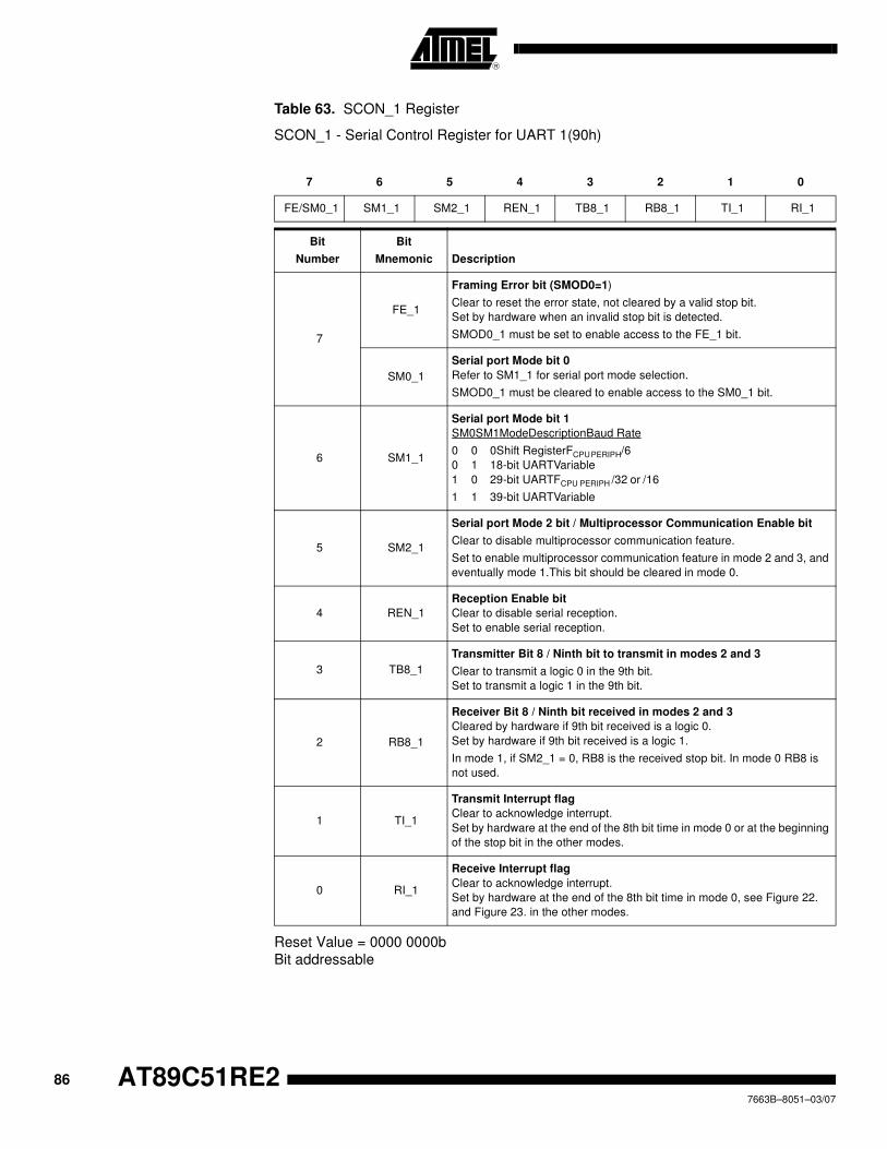
Table 63. SCON_1 Register
SCON_1 - Serial Control Register for UART 1(90h)
Reset Value = 0000 0000b
Bit addressable
7 6 5 4 3 2 1 0
FE/SM0_1 SM1_1 SM2_1 REN_1 TB8_1 RB8_1 TI_1 RI_1
Bit
Number
Bit
Mnemonic Description
7
FE_1
Framing Error bit (SMOD0=1)
Clear to reset the error state, not cleared by a valid stop bit.
Set by hardware when an invalid stop bit is detected.
SMOD0_1 must be set to enable access to the FE_1 bit.
SM0_1
Serial port Mode bit 0
Refer to SM1_1 for serial port mode selection.
SMOD0_1 must be cleared to enable access to the SM0_1 bit.
6 SM1_1
Serial port Mode bit 1
SM0SM1ModeDescriptionBaud Rate
0 0 0Shift RegisterFCPU PERIPH/6
0 1 18-bit UARTVariable
1 0 29-bit UARTFCPU PERIPH /32 or /16
1 1 39-bit UARTVariable
5 SM2_1
Serial port Mode 2 bit / Multiprocessor Communication Enable bit
Clear to disable multiprocessor communication feature.
Set to enable multiprocessor communication feature in mode 2 and 3, and
eventually mode 1.This bit should be cleared in mode 0.
4 REN_1
Reception Enable bit
Clear to disable serial reception.
Set to enable serial reception.
3 TB8_1
Transmitter Bit 8 / Ninth bit to transmit in modes 2 and 3
Clear to transmit a logic 0 in the 9th bit.
Set to transmit a logic 1 in the 9th bit.
2 RB8_1
Receiver Bit 8 / Ninth bit received in modes 2 and 3
Cleared by hardware if 9th bit received is a logic 0.
Set by hardware if 9th bit received is a logic 1.
In mode 1, if SM2_1 = 0, RB8 is the received stop bit. In mode 0 RB8 is
not used.
1 TI_1
Transmit Interrupt flag
Clear to acknowledge interrupt.
Set by hardware at the end of the 8th bit time in mode 0 or at the beginning
of the stop bit in the other modes.
0 RI_1
Receive Interrupt flag
Clear to acknowledge interrupt.
Set by hardware at the end of the 8th bit time in mode 0, see Figure 22.
and Figure 23. in the other modes.
86 AT89C51RE27663B–8051–03/07

AT89C51RE2
Table 64. Example of Computed Value When X2=1, SMOD1=1, SPD=1
Table 65. Example of Computed Value When X2=0, SMOD1=0, SPD=0
The baud rate generator can be used for mode 1 or 3 (refer to Figure 24.), but also for
mode 0 for UART, thanks to the bit SRC located in BDRCON register (Table 72.)
UART Registers Table 66. SBUF_0 register
SBUF_0 - Serial Buffer Register for UART 0(99h)
Reset Value = XXXX XXXXb
Table 67. BRL_0 register
BRL_0 - Baud Rate Reload Register for the internal baud rate generator 0 (9Ah)
Reset Value = 0000 0000b
Baud Rates FOSC = 16. 384 MHz FOSC = 24MHz
BRL Error (%) BRL Error (%)
115200 247 1.23 243 0.16
57600 238 1.23 230 0.16
38400 229 1.23 217 0.16
28800 220 1.23 204 0.16
19200 203 0.63 178 0.16
9600 149 0.31 100 0.16
4800 43 1.23 - -
Baud Rates FOSC = 16. 384 MHz FOSC = 24MHz
BRL Error (%) BRL Error (%)
4800 247 1.23 243 0.16
2400 238 1.23 230 0.16
1200 220 1.23 202 3.55
600 185 0.16 152 0.16
7 6 5 4 3 2 1 0
7 6 5 4 3 2 1 0
87
7663B–8051–03/07

Table 68. SBUF_1 Register
SBUF - Serial Buffer Register for UART 1(C1h)
Reset Value = XXXX XXXXb
Table 69. BRL_1 Register
BRL - Baud Rate Reload Register for the internal baud rate generator 1 (BBh)
Reset Value = 0000 0000b
7 6 5 4 3 2 1 0
7 6 5 4 3 2 1 0
88 AT89C51RE27663B–8051–03/07

AT89C51RE2
Table 70. T2CON Register
T2CON - Timer 2 Control Register (C8h)
Reset Value = 0000 0000b
Bit addressable
7 6 5 4 3 2 1 0
TF2 EXF2 RCLK TCLK EXEN2 TR2 C/T2# CP/RL2#
Bit
Number
Bit
Mnemonic Description
7 TF2
Timer 2 overflow Flag
Must be cleared by software.
Set by hardware on timer 2 overflow, if RCLK = 0 and TCLK = 0.
6 EXF2
Timer 2 External Flag
Set when a capture or a reload is caused by a negative transition on T2EX pin if
EXEN2=1.
When set, causes the CPU to vector to timer 2 interrupt routine when timer 2
interrupt is enabled.
Must be cleared by software. EXF2 doesn’t cause an interrupt in Up/down
counter mode (DCEN = 1)
5 RCLK
Receive Clock bit for UART
Cleared to use timer 1 overflow as receive clock for serial port in mode 1 or 3.
Set to use timer 2 overflow as receive clock for serial port in mode 1 or 3.
4 TCLK
Transmit Clock bit for UART
Cleared to use timer 1 overflow as transmit clock for serial port in mode 1 or 3.
Set to use timer 2 overflow as transmit clock for serial port in mode 1 or 3.
3 EXEN2
Timer 2 External Enable bit
Cleared to ignore events on T2EX pin for timer 2 operation.
Set to cause a capture or reload when a negative transition on T2EX pin is
detected, if timer 2 is not used to clock the serial port.
2 TR2
Timer 2 Run control bit
Cleared to turn off timer 2.
Set to turn on timer 2.
1 C/T2#
Timer/Counter 2 select bit
Cleared for timer operation (input from internal clock system: FCLK PERIPH).
Set for counter operation (input from T2 input pin, falling edge trigger). Must be
0 for clock out mode.
0 CP/RL2#
Timer 2 Capture/Reload bit
If RCLK=1 or TCLK=1, CP/RL2# is ignored and timer is forced to auto-reload on
timer 2 overflow.
Cleared to auto-reload on timer 2 overflows or negative transitions on T2EX pin
if EXEN2=1.
Set to capture on negative transitions on T2EX pin if EXEN2=1.
89
7663B–8051–03/07

Table 71. PCON Register
PCON - Power Control Register (87h)
Reset Value = 00X1 0000b
Not bit addressable
Power-off flag reset value will be 1 only after a power on (cold reset). A warm reset
doesn’t affect the value of this bit.
7 6 5 4 3 2 1 0
SMOD1_0 SMOD0_0 - POF GF1 GF0 PD IDL
Bit
Number
Bit
Mnemonic Description
7 SMOD1_0Serial port Mode bit 1 for UART
Set to select double baud rate in mode 1, 2 or 3.
6 SMOD0_0
Serial port Mode bit 0 for UART
Cleared to select SM0 bit in SCON register.
Set to select FE bit in SCON register.
5 -Reserved
The value read from this bit is indeterminate. Do not set this bit.
4 POF
Power-Off Flag
Cleared to recognize next reset type.
Set by hardware when VCC rises from 0 to its nominal voltage. Can also be set
by software.
3 GF1
General purpose Flag
Cleared by user for general purpose usage.
Set by user for general purpose usage.
2 GF0
General purpose Flag
Cleared by user for general purpose usage.
Set by user for general purpose usage.
1 PD
Power-Down mode bit
Cleared by hardware when reset occurs.
Set to enter power-down mode.
0 IDL
Idle mode bit
Cleared by hardware when interrupt or reset occurs.
Set to enter idle mode.
90 AT89C51RE27663B–8051–03/07

AT89C51RE2
Table 72. BDRCON_0 Register
BDRCON_0 - Baud Rate Control Register (9Bh)
Reset Value = XXX0 0000b
Not bit addressablef
7 6 5 4 3 2 1 0
- - - BRR_0 TBCK_0 RBCK_0 SPD_0 SRC_0
Bit
Number
Bit
Mnemonic Description
7 -Reserved
The value read from this bit is indeterminate. Do not set this bit
6 -Reserved
The value read from this bit is indeterminate. Do not set this bit
5 -Reserved
The value read from this bit is indeterminate. Do not set this bit.
4 BRR_0
Baud Rate Run Control bit
Cleared to stop the internal Baud Rate Generator.
Set to start the internal Baud Rate Generator.
3 TBCK_0
Transmission Baud rate Generator Selection bit for UART
Cleared to select Timer 1 or Timer 2 for the Baud Rate Generator.
Set to select internal Baud Rate Generator.
2 RBCK_0
Reception Baud Rate Generator Selection bit for UART
Cleared to select Timer 1 or Timer 2 for the Baud Rate Generator.
Set to select internal Baud Rate Generator.
1 SPD_0
Baud Rate Speed Control bit for UART
Cleared to select the SLOW Baud Rate Generator.
Set to select the FAST Baud Rate Generator.
0 SRC_0
Baud Rate Source select bit in Mode 0 for UART
Cleared to select FOSC/12 as the Baud Rate Generator (FCLK PERIPH/6 in X2
mode).
Set to select the internal Baud Rate Generator for UARTs in mode 0.
91
7663B–8051–03/07

Table 73. BDRCON_1 Register
BDRCON - Baud Rate Control Register (BCh)
Reset Value = 0000 0000b
Not bit addressablef
7 6 5 4 3 2 1 0
SMOD1_1 SMOD0_1 - BRR_1 TBCK_1 RBCK_1 SPD_1 SRC_1
Bit
Number
Bit
Mnemonic Description
7 SMOD1_1Serial port Mode bit 1 for UART 1
Set to select double baud rate in mode 1, 2 or 3.
6 SMOD0_1
Serial port Mode bit 0 for UART 1
Cleared to select SM0 bit in SCON register.
Set to select FE bit in SCON register.
5 -Reserved
The value read from this bit is indeterminate. Do not set this bit.
4 BRR_1
Baud Rate Run Control bit
Cleared to stop the internal Baud Rate Generator.
Set to start the internal Baud Rate Generator.
3 TBCK_1
Transmission Baud rate Generator Selection bit for UART 1
Cleared to select Timer 1 or Timer 2 for the Baud Rate Generator.
Set to select internal Baud Rate Generator.
2 RBCK_1
Reception Baud Rate Generator Selection bit for UART 1
Cleared to select Timer 1 or Timer 2 for the Baud Rate Generator.
Set to select internal Baud Rate Generator.
1 SPD_1
Baud Rate Speed Control bit for UART 1
Cleared to select the SLOW Baud Rate Generator.
Set to select the FAST Baud Rate Generator.
0 SRC_1
Baud Rate Source select bit in Mode 0 for UART 1
Cleared to select FOSC/12 as the Baud Rate Generator (FCLK PERIPH/6 in X2
mode).
Set to select the internal Baud Rate Generator for UARTs in mode 0.
92 AT89C51RE27663B–8051–03/07

AT89C51RE2
Interrupt System The AT89C51RE2 has a total of 10 interrupt vectors: two external interrupts (INT0 and
INT1), three timer interrupts (timers 0, 1 and 2), two serial ports interrupts, SPI interrupt,
Keyboard interrupt and the PCA global interrupt. These interrupts are shown in Figure
28.
Figure 28. Interrupt Control System
Each of the interrupt sources can be individually enabled or disabled by setting or clear-
ing a bit in the Interrupt Enable register (Table 78 and Table 76). This register also
contains a global disable bit, which must be cleared to disable all interrupts at once.
Each interrupt source can also be individually programmed to one out of four priority lev-
els by setting or clearing a bit in the Interrupt Priority register (Table 79) and in the
Interrupt Priority High register (Table 77 and Table 78) shows the bit values and priority
levels associated with each combination.
IE1
0
3
High priority
interrupt
Interrupt
polling
sequence, decreasing from
high to low priority
Low priority
interrupt
Global DisableIndividual Enable
EXF2
TF2
TI
RI
TF0
INT0
INT1
TF1
IPH, IPL
IE0
0
3
0
3
0
3
0
3
0
3
0
3
PCA IT
KBD IT
SPI IT
0
3
0
3
TI_1
RI_1
0
3
93
7663B–8051–03/07

RegistersTable 74. Priority Level Bit Values
A low-priority interrupt can be interrupted by a high priority interrupt, but not by another
low-priority interrupt. A high-priority interrupt can’t be interrupted by any other interrupt
source.
If two interrupt requests of different priority levels are received simultaneously, the
request of higher priority level is serviced. If interrupt requests of the same priority level
are received simultaneously, an internal polling sequence determines which request is
serviced. Thus within each priority level there is a second priority structure determined
by the polling sequence.
IPH. x IPL. x Interrupt Level Priority
0 0 0 (Lowest)
0 1 1
1 0 2
1 1 3 (Highest)
94 AT89C51RE27663B–8051–03/07

AT89C51RE2
Table 75. IEN0 Register
IEN0 - Interrupt Enable Register (A8h)
Reset Value = 0000 0000b
Bit addressable
7 6 5 4 3 2 1 0
EA EC ET2 ES ET1 EX1 ET0 EX0
Bit
Number
Bit
Mnemonic Description
7 EA
Enable All interrupt bit
Cleared to disable all interrupts.
Set to enable all interrupts.
6 EC
PCA interrupt enable bit
Cleared to disable.
Set to enable.
5 ET2
Timer 2 overflow interrupt Enable bit
Cleared to disable timer 2 overflow interrupt.
Set to enable timer 2 overflow interrupt.
4 ES
Serial port 0 Enable bit
Cleared to disable serial port interrupt.
Set to enable serial port interrupt.
3 ET1
Timer 1 overflow interrupt Enable bit
Cleared to disable timer 1 overflow interrupt.
Set to enable timer 1 overflow interrupt.
2 EX1
External interrupt 1 Enable bit
Cleared to disable external interrupt 1.
Set to enable external interrupt 1.
1 ET0
Timer 0 overflow interrupt Enable bit
Cleared to disable timer 0 overflow interrupt.
Set to enable timer 0 overflow interrupt.
0 EX0
External interrupt 0 Enable bit
Cleared to disable external interrupt 0.
Set to enable external interrupt 0.
95
7663B–8051–03/07

Table 76. IPL0 Register
IPL0 - Interrupt Priority Register (B8h)
Reset Value = X000 0000b
Bit addressable
7 6 5 4 3 2 1 0
- PPCL PT2L PSL PT1L PX1L PT0L PX0L
Bit
Number
Bit
Mnemonic Description
7 -Reserved
The value read from this bit is indeterminate. Do not set this bit.
6 PPCLPCA interrupt Priority bit
Refer to PPCH for priority level.
5 PT2LTimer 2 overflow interrupt Priority bit
Refer to PT2H for priority level.
4 PSLSerial port 0 Priority bit
Refer to PSH for priority level.
3 PT1LTimer 1 overflow interrupt Priority bit
Refer to PT1H for priority level.
2 PX1LExternal interrupt 1 Priority bit
Refer to PX1H for priority level.
1 PT0LTimer 0 overflow interrupt Priority bit
Refer to PT0H for priority level.
0 PX0LExternal interrupt 0 Priority bit
Refer to PX0H for priority level.
96 AT89C51RE27663B–8051–03/07
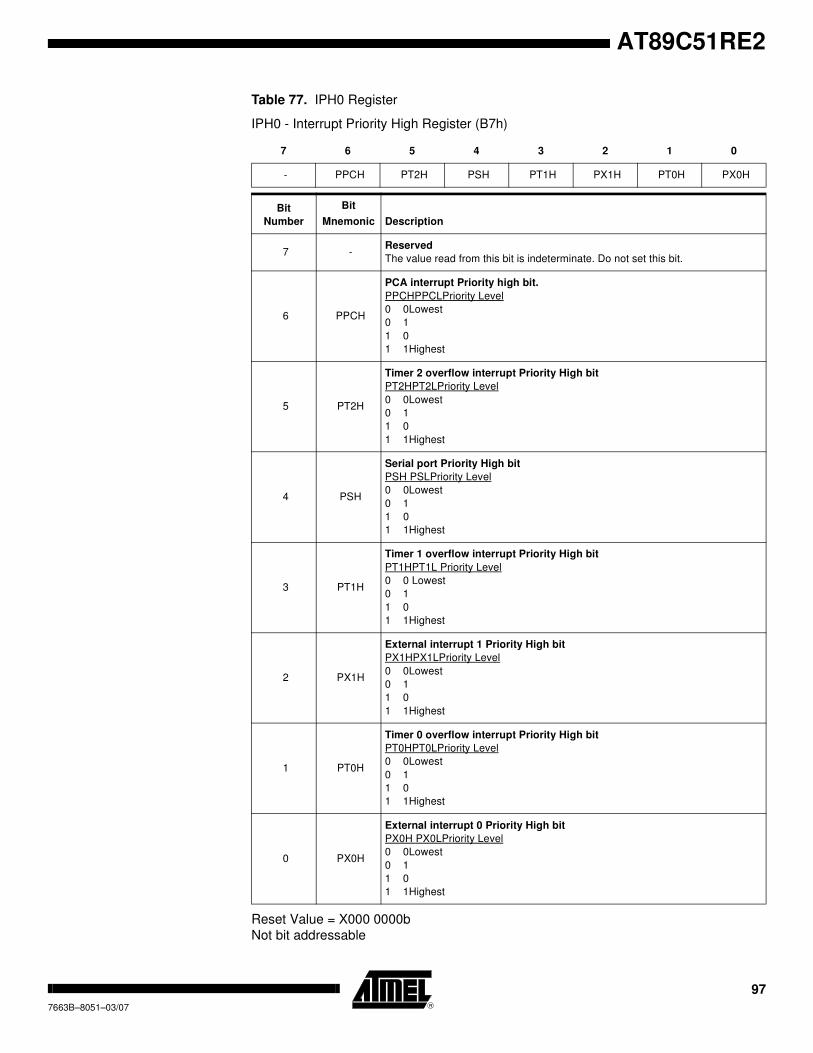
AT89C51RE2
Table 77. IPH0 Register
IPH0 - Interrupt Priority High Register (B7h)
Reset Value = X000 0000b
Not bit addressable
7 6 5 4 3 2 1 0
- PPCH PT2H PSH PT1H PX1H PT0H PX0H
Bit
Number
Bit
Mnemonic Description
7 -Reserved
The value read from this bit is indeterminate. Do not set this bit.
6 PPCH
PCA interrupt Priority high bit.
PPCHPPCLPriority Level
0 0Lowest
0 1
1 0
1 1Highest
5 PT2H
Timer 2 overflow interrupt Priority High bit
PT2HPT2LPriority Level
0 0Lowest
0 1
1 0
1 1Highest
4 PSH
Serial port Priority High bit
PSH PSLPriority Level
0 0Lowest
0 1
1 0
1 1Highest
3 PT1H
Timer 1 overflow interrupt Priority High bit
PT1HPT1L Priority Level
0 0 Lowest
0 1
1 0
1 1 Highest
2 PX1H
External interrupt 1 Priority High bit
PX1HPX1LPriority Level
0 0Lowest
0 1
1 0
1 1Highest
1 PT0H
Timer 0 overflow interrupt Priority High bit
PT0HPT0LPriority Level
0 0Lowest
0 1
1 0
1 1Highest
0 PX0H
External interrupt 0 Priority High bit
PX0H PX0LPriority Level
0 0Lowest
0 1
1 0
1 1Highest
97
7663B–8051–03/07

Table 78. IEN1 Register
IEN1 - Interrupt Enable Register (B1h)
Reset Value = XXXX 00x0b
Bit addressable
7 6 5 4 3 2 1 0
- - - - ES_1 ESPI - EKBD
Bit
Number
Bit
Mnemonic Description
7 - Reserved
6 - Reserved
5 - Reserved
4 - Reserved
3 ES_1
Serial port 1 Enable bit
Cleared to disable serial port interrupt.
Set to enable serial port interrupt.
2 ESPI
SPI interrupt Enable bit
Cleared to disable SPI interrupt.
Set to enable SPI interrupt.
1 - Reserved
0 EKBD
Keyboard interrupt Enable bit
Cleared to disable keyboard interrupt.
Set to enable keyboard interrupt.
98 AT89C51RE27663B–8051–03/07

AT89C51RE2
Table 79. IPL1 Register
IPL1 - Interrupt Priority Register (B2h)
Reset Value = XXXX 00X0b
Bit addressable
7 6 5 4 3 2 1 0
- - - - PSL_1 SPIL - KBDL
Bit
Number
Bit
Mnemonic Description
7 -Reserved
The value read from this bit is indeterminate. Do not set this bit.
6 -Reserved
The value read from this bit is indeterminate. Do not set this bit.
5 -Reserved
The value read from this bit is indeterminate. Do not set this bit.
4 -Reserved
The value read from this bit is indeterminate. Do not set this bit.
3 PSL_1Serial port 1 Priority bit
Refer to PSH_1 for priority level.
2 SPILSPI interrupt Priority bit
Refer to SPIH for priority level.
1 - Reserved
0 KBDLKeyboard interrupt Priority bit
Refer to KBDH for priority level.
99
7663B–8051–03/07

Table 80. IPH1 Register
IPH1 - Interrupt Priority High Register (B3h)
Reset Value = XXXX 00X0b
Not bit addressable
7 6 5 4 3 2 1 0
- - - - PSH_1 SPIH - KBDH
Bit
Number
Bit
Mnemonic Description
7 -Reserved
The value read from this bit is indeterminate. Do not set this bit.
6 -Reserved
The value read from this bit is indeterminate. Do not set this bit.
5 -Reserved
The value read from this bit is indeterminate. Do not set this bit.
4 -Reserved
The value read from this bit is indeterminate. Do not set this bit.
3 PSH_1
Serial port 1 Priority High bit
PSH_1 PSL_1Priority Level
0 0Lowest
0 1
1 0
1 1Highest
2 SPIH
SPI interrupt Priority High bit
SPIH SPILPriority Level
0 0 Lowest
0 1
1 0
1 1 Highest
1 -Reserved
The value read from this bit is indeterminate. Do not set this bit.
0 KBDH
Keyboard interrupt Priority High bit
KB DH KBDLPriority Level
0 0 Lowest
0 1
1 0
1 1 Highest
100 AT89C51RE27663B–8051–03/07

AT89C51RE2
Interrupt Sources and Vector Addresses
Table 81. Interrupt Sources and Vector Addresses
Number Polling Priority Interrupt Source
Interrupt
Request
Vector
Address
0 0 Reset 0000h
1 1 INT0 IE0 0003h
2 2 Timer 0 TF0 000Bh
3 3 INT1 IE1 0013h
4 4 Timer 1 IF1 001Bh
5 6 UART0 RI+TI 0023h
6 7 Timer 2 TF2+EXF2 002Bh
7 5 PCA CF + CCFn (n = 0-4) 0033h
8 8 Keyboard KBDIT 003Bh
9 9 SPI SPIIT 004Bh
10 10 UART1 RI_1+TI_1 0053h
101
7663B–8051–03/07

Power Management
Introduction Two power reduction modes are implemented in the AT89C51RE2. The Idle mode and
the Power-Down mode. These modes are detailed in the following sections. In addition
to these power reduction modes, the clocks of the core and peripherals can be dynami-
cally divided by 2 using the X2 mode detailed in Section “Enhanced Features”, page 14.
Idle Mode Idle mode is a power reduction mode that reduces the power consumption. In this mode,
program execution halts. Idle mode freezes the clock to the CPU at known states while
the peripherals continue to be clocked. The CPU status before entering Idle mode is
preserved, i.e., the program counter and program status word register retain their data
for the duration of Idle mode. The contents of the SFRs and RAM are also retained. The
status of the Port pins during Idle mode is detailed in Table 82.
Entering Idle Mode To enter Idle mode, set the IDL bit in PCON register (see Table 83). The AT89C51RE2
enters Idle mode upon execution of the instruction that sets IDL bit. The instruction that
sets IDL bit is the last instruction executed.
Note: If IDL bit and PD bit are set simultaneously, the AT89C51RE2 enters Power-Down mode.
Then it does not go in Idle mode when exiting Power-Down mode.
Exiting Idle Mode There are two ways to exit Idle mode:
1. Generate an enabled interrupt.
– Hardware clears IDL bit in PCON register which restores the clock to the
CPU. Execution resumes with the interrupt service routine. Upon completion
of the interrupt service routine, program execution resumes with the
instruction immediately following the instruction that activated Idle mode.
The general purpose flags (GF1 and GF0 in PCON register) may be used to
indicate whether an interrupt occurred during normal operation or during Idle
mode. When Idle mode is exited by an interrupt, the interrupt service routine
may examine GF1 and GF0.
2. Generate a reset.
– A logic high on the RST pin clears IDL bit in PCON register directly and
asynchronously. This restores the clock to the CPU. Program execution
momentarily resumes with the instruction immediately following the
instruction that activated the Idle mode and may continue for a number of
clock cycles before the internal reset algorithm takes control. Reset
initializes the AT89C51RE2 and vectors the CPU to address C:0000h.
Note: During the time that execution resumes, the internal RAM cannot be accessed; however,
it is possible for the Port pins to be accessed. To avoid unexpected outputs at the Port
pins, the instruction immediately following the instruction that activated Idle mode should
not write to a Port pin or to the external RAM.
Power-Down Mode The Power-Down mode places the AT89C51RE2 in a very low power state. Power-
Down mode stops the oscillator, freezes all clock at known states. The CPU status prior
to entering Power-Down mode is preserved, i.e., the program counter, program status
word register retain their data for the duration of Power-Down mode. In addition, the SFR
102 AT89C51RE27663B–8051–03/07

AT89C51RE2
and RAM contents are preserved. The status of the Port pins during Power-Down mode
is detailed in Table 82.
Note: VCC may be reduced to as low as VRET during Power-Down mode to further reduce
power dissipation. Take care, however, that VDD is not reduced until Power-Down mode
is invoked.
Entering Power-Down Mode To enter Power-Down mode, set PD bit in PCON register. The AT89C51RE2 enters the
Power-Down mode upon execution of the instruction that sets PD bit. The instruction
that sets PD bit is the last instruction executed.
Exiting Power-Down ModeNote: If VCC was reduced during the Power-Down mode, do not exit Power-Down mode until
VCC is restored to the normal operating level.
There are two ways to exit the Power-Down mode:
1. Generate an enabled external interrupt.
– The AT89C51RE2 provides capability to exit from Power-Down using INT0#,
INT1#.
Hardware clears PD bit in PCON register which starts the oscillator and
restores the clocks to the CPU and peripherals. Using INTx# input,
execution resumes when the input is released (see Figure 29). Execution
resumes with the interrupt service routine. Upon completion of the interrupt
service routine, program execution resumes with the instruction immediately
following the instruction that activated Power-Down mode.
Note: The external interrupt used to exit Power-Down mode must be configured as level sensi-
tive (INT0# and INT1#) and must be assigned the highest priority. In addition, the
duration of the interrupt must be long enough to allow the oscillator to stabilize. The exe-
cution will only resume when the interrupt is deasserted.
Note: Exit from power-down by external interrupt does not affect the SFRs nor the internal RAM
content.
Figure 29. Power-Down Exit Waveform Using INT1:0#
2. Generate a reset.
– A logic high on the RST pin clears PD bit in PCON register directly and
asynchronously. This starts the oscillator and restores the clock to the CPU
and peripherals. Program execution momentarily resumes with the
instruction immediately following the instruction that activated Power-Down
mode and may continue for a number of clock cycles before the internal
reset algorithm takes control. Reset initializes the AT89C51RE2 and vectors
the CPU to address 0000h.
Note: During the time that execution resumes, the internal RAM cannot be accessed; however,
it is possible for the Port pins to be accessed. To avoid unexpected outputs at the Port
INT1:0#
OSC
Power-down phase Oscillator restart phase Active phaseActive phase
103
7663B–8051–03/07

pins, the instruction immediately following the instruction that activated the Power-Down
mode should not write to a Port pin or to the external RAM.
Note: Exit from power-down by reset redefines all the SFRs, but does not affect the internal
RAM content.
Table 82. Pin Conditions in Special Operating Modes
Mode Port 0 Port 1 Port 2 Port 3 Port 4 ALE PSEN#
Reset Floating High High High High High High
Idle
(internal
code)
Data Data Data Data Data High High
Idle
(external
code)
Floating Data Data Data Data High High
Power-
Down(inter
nal code)
Data Data Data Data Data Low Low
Power-
Down
(external
code)
Floating Data Data Data Data Low Low
104 AT89C51RE27663B–8051–03/07

AT89C51RE2
Registers Table 83. PCON Register
PCON (87:h) Power configuration Register
Reset Value= XXXX 0000b
7 6 5 4 3 2 1 0
SMOD1 SMOD0 - POF GF1 GF0 PD IDL
Bit
Number
Bit
Mnemonic Description
7 SMOD1Serial Port Mode bit 1
Set to select double baud rate in mode 1, 2 or 3.
6 SMOD0
Serial Port Mode bit 0
Cleared to select SM0 bit in SCON register.
Set to select FE bit in SCON register.
5 - reserved
4 POF
Power-Off Flag
Cleared to recognize next reset type.
Set by hardware when VCC rises from 0 to its nominal voltage. Can also be set
by software.
3 GF1
General Purpose flag 1
One use is to indicate whether an interrupt occurred during normal operation or
during Idle mode.
2 GF0
General Purpose flag 0
One use is to indicate whether an interrupt occurred during normal operation or
during Idle mode.
1 PD
Power-Down Mode bit
Cleared by hardware when an interrupt or reset occurs.
Set to activate the Power-Down mode.
If IDL and PD are both set, PD takes precedence.
0 IDL
Idle Mode bit
Cleared by hardware when an interrupt or reset occurs.
Set to activate the Idle mode.
If IDL and PD are both set, PD takes precedence.
105
7663B–8051–03/07

Oscillator To optimize the power consumption and execution time needed for a specific task, an
internal prescaler feature has been implemented between the oscillator and the CPU
and peripherals.
Registers Table 84. CKRL Register
CKRL – Clock Reload Register (97h)
Reset Value = 1111 1111b
Not bit addressable
Table 85. PCON Register
PCON – Power Control Register (87h)
7 6 5 4 3 2 1 0
CKRL7 CKRL6 CKRL5 CKRL4 CKRL3 CKRL2 CKRL1 CKRL0
Bit Number Mnemonic Description
7:0 CKRLClock Reload Register
Prescaler value
7 6 5 4 3 2 1 0
SMOD1 SMOD0 - POF GF1 GF0 PD IDL
Bit Number Bit Mnemonic Description
7 SMOD1Serial Port Mode bit 1
Set to select double baud rate in mode 1, 2 or 3.
6 SMOD0
Serial Port Mode bit 0
Cleared to select SM0 bit in SCON register.
Set to select FE bit in SCON register.
5 -Reserved
The value read from this bit is indeterminate. Do not set this bit.
4 POF
Power-off Flag
Cleared by software to recognize the next reset type.
Set by hardware when VCC rises from 0 to its nominal voltage. Can
also be set by software.
3 GF1
General-purpose Flag
Cleared by software for general-purpose usage.
Set by software for general-purpose usage.
2 GF0
General-purpose Flag
Cleared by software for general-purpose usage.
Set by software for general-purpose usage.
1 PD
Power-down Mode bit
Cleared by hardware when reset occurs.
Set to enter power-down mode.
0 IDL
Idle Mode bit
Cleared by hardware when interrupt or reset occurs.
Set to enter idle mode.
106 AT89C51RE27663B–8051–03/07

AT89C51RE2
Reset Value = 00X1 0000b Not bit addressable
Functional Block Diagram
Figure 30. Functional Oscillator Block Diagram
Prescaler Divider • A hardware RESET puts the prescaler divider in the following state:
• CKRL = FFh: FCLK CPU = FCLK PERIPH = FOSC/2 (Standard C51 feature)
• Any value between FFh down to 00h can be written by software into CKRL register
in order to divide frequency of the selected oscillator:
• CKRL = 00h: minimum frequency
FCLK CPU = FCLK PERIPH = FOSC/1020 (Standard Mode)
FCLK CPU = FCLK PERIPH = FOSC/510 (X2 Mode)
• CKRL = FFh: maximum frequency
FCLK CPU = FCLK PERIPH = FOSC/2 (Standard Mode)
FCLK CPU = FCLK PERIPH = FOSC (X2 Mode)
FCLK CPU and FCLK PERIPH
In X2 Mode, for CKRL<>0xFF:
In X1 Mode, for CKRL<>0xFF then:
Xtal2
Xtal1
Osc
CLK
Idle
CPU Clock
CKRL
Reload
8-bit
Prescaler-Divider
Reset
Peripheral Clock
:2
X2
0
1
FOSC
CKCON0
CLKPeriph
CPU
CKRL = 0xFF?
0
1
FCPU F=CLKPERIPH
FOSC
2 255 CKRL–( )×-----------------------------------------------=
FCPU F=CLKPERIPH
FOSC
4 255 CKRL–( )×-----------------------------------------------=
107
7663B–8051–03/07

Hardware Watchdog
Timer
The WDT is intended as a recovery method in situations where the CPU may be sub-
jected to software upset. The WDT consists of a 14-bit counter and the WatchDog Timer
ReSeT (WDTRST) SFR. The WDT is by default disabled from exiting reset. To enable
the WDT, user must write 01EH and 0E1H in sequence to the WDTRST, SFR location
0A6H. When WDT is enabled, it will increment every machine cycle while the oscillator
is running and there is no way to disable the WDT except through reset (either hardware
reset or WDT overflow reset). When WDT overflows, it will drive an output RESET HIGH
pulse at the RST-pin.
Using the WDT To enable the WDT, user must write 01EH and 0E1H in sequence to the WDTRST, SFR
location 0A6H. When WDT is enabled, the user needs to service it by writing to 01EH
and 0E1H to WDTRST to avoid WDT overflow. The 14-bit counter overflows when it
reaches 16383 (3FFFH) and this will reset the device. When WDT is enabled, it will
increment every machine cycle while the oscillator is running. This means the user must
reset the WDT at least every 16383 machine cycle. To reset the WDT the user must
write 01EH and 0E1H to WDTRST. WDTRST is a write only register. The WDT counter
cannot be read or written. When WDT overflows, it will generate an output RESET pulse
at the RST-pin. The RESET pulse duration is 96 x TCLK PERIPH, where TCLK PERIPH= 1/FCLK
PERIPH. To make the best use of the WDT, it should be serviced in those sections of code
that will periodically be executed within the time required to prevent a WDT reset.
To have a more powerful WDT, a 27 counter has been added to extend the Time-out
capability, ranking from 16ms to 2s @ FOSCA = 12MHz. To manage this feature, refer to
WDTPRG register description, Table 86.
Table 86. WDTRST Register
WDTRST - Watchdog Reset Register (0A6h)
Reset Value = XXXX XXXXb
Write only, this SFR is used to reset/enable the WDT by writing 01EH then 0E1H in
sequence.
7 6 5 4 3 2 1 0
- - - - - - - -
108 AT89C51RE27663B–8051–03/07
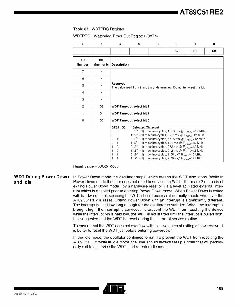
AT89C51RE2
Table 87. WDTPRG Register
WDTPRG - Watchdog Timer Out Register (0A7h)
Reset value = XXXX X000
WDT During Power Down and Idle
In Power Down mode the oscillator stops, which means the WDT also stops. While in
Power Down mode the user does not need to service the WDT. There are 2 methods of
exiting Power Down mode: by a hardware reset or via a level activated external inter-
rupt which is enabled prior to entering Power Down mode. When Power Down is exited
with hardware reset, servicing the WDT should occur as it normally should whenever the
AT89C51RE2 is reset. Exiting Power Down with an interrupt is significantly different.
The interrupt is held low long enough for the oscillator to stabilize. When the interrupt is
brought high, the interrupt is serviced. To prevent the WDT from resetting the device
while the interrupt pin is held low, the WDT is not started until the interrupt is pulled high.
It is suggested that the WDT be reset during the interrupt service routine.
To ensure that the WDT does not overflow within a few states of exiting of powerdown, it
is better to reset the WDT just before entering powerdown.
In the Idle mode, the oscillator continues to run. To prevent the WDT from resetting the
AT89C51RE2 while in Idle mode, the user should always set up a timer that will periodi-
cally exit Idle, service the WDT, and re-enter Idle mode.
7 6 5 4 3 2 1 0
- - - - - S2 S1 S0
Bit
Number
Bit
Mnemonic Description
7 -
Reserved
The value read from this bit is undetermined. Do not try to set this bit.
6 -
5 -
4 -
3 -
2 S2 WDT Time-out select bit 2
1 S1 WDT Time-out select bit 1
0 S0 WDT Time-out select bit 0
S2S1 S0 Selected Time-out
0 0 0 (214 - 1) machine cycles, 16. 3 ms @ FOSCA =12 MHz
0 0 1 (215 - 1) machine cycles, 32.7 ms @ FOSCA=12 MHz
0 1 0 (216 - 1) machine cycles, 65. 5 ms @ FOSCA=12 MHz
0 1 1 (217 - 1) machine cycles, 131 ms @ FOSCA=12 MHz
1 0 0 (218 - 1) machine cycles, 262 ms @ FOSCA=12 MHz
1 0 1 (219 - 1) machine cycles, 542 ms @ FOSCA=12 MHz
1 1 0 (220 - 1) machine cycles, 1.05 s @ FOSCA=12 MHz
1 1 1 (221 - 1) machine cycles, 2.09 s @ FOSCA=12 MHz
109
7663B–8051–03/07

110 AT89C51RE27663B–8051–03/07
Reduced EMI Mode The ALE signal is used to demultiplex address and data buses on port 0 when used with
external program or data memory. Nevertheless, during internal code execution, ALE
signal is still generated. In order to reduce EMI, ALE signal can be disabled by setting
AO bit.
The AO bit is located in AUXR register at bit location 0. As soon as AO is set, ALE is no
longer output but remains active during MOVX and MOVC instructions and external
fetches. During ALE disabling, ALE pin is weakly pulled high.
Table 88. AUXR Register
AUXR - Auxiliary Register (8Eh)
Reset Value = XX00 10’HSB. XRAM’0b
Not bit addressable
7 6 5 4 3 2 1 0
- - M0 XRS2 XRS1 XRS0 EXTRAM AO
Bit
Number
Bit
Mnemonic Description
7 -Reserved
The value read from this bit is indeterminate. Do not set this bit.
6 -Reserved
The value read from this bit is indeterminate. Do not set this bit.
5 M0
Pulse length
Cleared to stretch MOVX control: the RD/ and the WR/ pulse length is 6 clock
periods (default).
Set to stretch MOVX control: the RD/ and the WR/ pulse length is 30 clock
periods.
4 XRS2 XRAM Size
XRS2 XRS1XRS0XRAM size
0 0 0 256 bytes
0 0 1 512 bytes
0 1 0 768 bytes(default)
0 1 1 1024 bytes
1 0 0 1792 bytes
3 XRS1
2 XRS0
1 EXTRAM
EXTRAM bit
Cleared to access internal XRAM using movx @ Ri/ @ DPTR.
Set to access external memory.
Programmed by hardware after Power-up regarding Hardware Security Byte
(HSB), default setting, XRAM selected.
0 AO
ALE Output bit
Cleared, ALE is emitted at a constant rate of 1/6 the oscillator frequency (or 1/3 if
X2 mode is used). (default) Set, ALE is active only during a MOVX or MOVC
instruction is used.

AT89C51RE2
Keyboard Interface The AT89C51RE2 implements a keyboard interface allowing the connection of a
8 x n matrix keyboard. It is based on 8 inputs with programmable interrupt capability on
both high or low level. These inputs are available as alternate function of P1 and allow to
exit from idle and power down modes.
The keyboard interface interfaces with the C51 core through 3 special function registers:
KBLS, the Keyboard Level Selection register (Table 91), KBE, The Keyboard interrupt
Enable register (Table 90), and KBF, the Keyboard Flag register (Table 89).
Interrupt The keyboard inputs are considered as 8 independent interrupt sources sharing the
same interrupt vector. An interrupt enable bit (KBD in IE1) allows global enable or dis-
able of the keyboard interrupt (see Figure 31). As detailed in Figure 32 each keyboard
input has the capability to detect a programmable level according to KBLS. x bit value.
Level detection is then reported in interrupt flags KBF. x that can be masked by software
using KBE. x bits.
This structure allow keyboard arrangement from 1 by n to 8 by n matrix and allow usage
of P1 inputs for other purpose.
Figure 31. Keyboard Interface Block Diagram
Figure 32. Keyboard Input Circuitry
Power Reduction Mode P1 inputs allow exit from idle and power down modes as detailed in Section “Power
Management”, page 102.
P1:x
KBE. x
KBF. x
KBLS. x
0
1
Vcc
Internal Pullup
P1.0
Keyboard InterfaceInterrupt Request
KBDIE1
Input Circuitry
P1.1 Input Circuitry
P1.2 Input Circuitry
P1.3 Input Circuitry
P1.4 Input Circuitry
P1.5 Input Circuitry
P1.6 Input Circuitry
P1.7 Input Circuitry
KBDIT
111
7663B–8051–03/07

Registers Table 89. KBF Register
KBF-Keyboard Flag Register (9Eh)
Reset Value= 0000 0000b
7 6 5 4 3 2 1 0
KBF7 KBF6 KBF5 KBF4 KBF3 KBF2 KBF1 KBF0
Bit
Number
Bit
Mnemonic Description
7 KBF7
Keyboard line 7 flag
Set by hardware when the Port line 7 detects a programmed level. It generates a
Keyboard interrupt request if the KBKBIE. 7 bit in KBIE register is set.
Must be cleared by software.
6 KBF6
Keyboard line 6 flag
Set by hardware when the Port line 6 detects a programmed level. It generates a
Keyboard interrupt request if the KBIE. 6 bit in KBIE register is set.
Must be cleared by software.
5 KBF5
Keyboard line 5 flag
Set by hardware when the Port line 5 detects a programmed level. It generates a
Keyboard interrupt request if the KBIE. 5 bit in KBIE register is set.
Must be cleared by software.
4 KBF4
Keyboard line 4 flag
Set by hardware when the Port line 4 detects a programmed level. It generates a
Keyboard interrupt request if the KBIE. 4 bit in KBIE register is set.
Must be cleared by software.
3 KBF3
Keyboard line 3 flag
Set by hardware when the Port line 3 detects a programmed level. It generates a
Keyboard interrupt request if the KBIE. 3 bit in KBIE register is set.
Must be cleared by software.
2 KBF2
Keyboard line 2 flag
Set by hardware when the Port line 2 detects a programmed level. It generates a
Keyboard interrupt request if the KBIE. 2 bit in KBIE register is set.
Must be cleared by software.
1 KBF1
Keyboard line 1 flag
Set by hardware when the Port line 1 detects a programmed level. It generates a
Keyboard interrupt request if the KBIE. 1 bit in KBIE register is set.
Must be cleared by software.
0 KBF0
Keyboard line 0 flag
Set by hardware when the Port line 0 detects a programmed level. It generates a
Keyboard interrupt request if the KBIE. 0 bit in KBIE register is set.
Must be cleared by software.
112 AT89C51RE27663B–8051–03/07

AT89C51RE2
Table 90. KBE Register
KBE-Keyboard Input Enable Register (9Dh)
Reset Value= 0000 0000b
7 6 5 4 3 2 1 0
KBE7 KBE6 KBE5 KBE4 KBE3 KBE2 KBE1 KBE0
Bit
Number
Bit
Mnemonic Description
7 KBE7
Keyboard line 7 Enable bit
Cleared to enable standard I/O pin.
Set to enable KBF. 7 bit in KBF register to generate an interrupt request.
6 KBE6
Keyboard line 6 Enable bit
Cleared to enable standard I/O pin.
Set to enable KBF. 6 bit in KBF register to generate an interrupt request.
5 KBE5
Keyboard line 5 Enable bit
Cleared to enable standard I/O pin.
Set to enable KBF. 5 bit in KBF register to generate an interrupt request.
4 KBE4
Keyboard line 4 Enable bit
Cleared to enable standard I/O pin.
Set to enable KBF. 4 bit in KBF register to generate an interrupt request.
3 KBE3
Keyboard line 3 Enable bit
Cleared to enable standard I/O pin.
Set to enable KBF. 3 bit in KBF register to generate an interrupt request.
2 KBE2
Keyboard line 2 Enable bit
Cleared to enable standard I/O pin.
Set to enable KBF. 2 bit in KBF register to generate an interrupt request.
1 KBE1
Keyboard line 1 Enable bit
Cleared to enable standard I/O pin.
Set to enable KBF. 1 bit in KBF register to generate an interrupt request.
0 KBE0
Keyboard line 0 Enable bit
Cleared to enable standard I/O pin.
Set to enable KBF. 0 bit in KBF register to generate an interrupt request.
113
7663B–8051–03/07

Table 91. KBLS Register
KBLS-Keyboard Level Selector Register (9Ch)
Reset Value= 0000 0000b
7 6 5 4 3 2 1 0
KBLS7 KBLS6 KBLS5 KBLS4 KBLS3 KBLS2 KBLS1 KBLS0
Bit
Number
Bit
Mnemonic Description
7 KBLS7
Keyboard line 7 Level Selection bit
Cleared to enable a low level detection on Port line 7.
Set to enable a high level detection on Port line 7.
6 KBLS6
Keyboard line 6 Level Selection bit
Cleared to enable a low level detection on Port line 6.
Set to enable a high level detection on Port line 6.
5 KBLS5
Keyboard line 5 Level Selection bit
Cleared to enable a low level detection on Port line 5.
Set to enable a high level detection on Port line 5.
4 KBLS4
Keyboard line 4 Level Selection bit
Cleared to enable a low level detection on Port line 4.
Set to enable a high level detection on Port line 4.
3 KBLS3
Keyboard line 3 Level Selection bit
Cleared to enable a low level detection on Port line 3.
Set to enable a high level detection on Port line 3.
2 KBLS2
Keyboard line 2 Level Selection bit
Cleared to enable a low level detection on Port line 2.
Set to enable a high level detection on Port line 2.
1 KBLS1
Keyboard line 1 Level Selection bit
Cleared to enable a low level detection on Port line 1.
Set to enable a high level detection on Port line 1.
0 KBLS0
Keyboard line 0 Level Selection bit
Cleared to enable a low level detection on Port line 0.
Set to enable a high level detection on Port line 0.
114 AT89C51RE27663B–8051–03/07

AT89C51RE2
Serial Port Interface
(SPI)
The Serial Peripheral Interface Module (SPI) allows full-duplex, synchronous, serial
communication between the MCU and peripheral devices, including other MCUs.
Features Features of the SPI Module include the following:
• Full-duplex, three-wire synchronous transfers
• Master or Slave operation
• Six programmable Master clock rates in master mode
• Serial clock with programmable polarity and phase
• Master Mode fault error flag with MCU interrupt capability
Signal Description Figure 33 shows a typical SPI bus configuration using one Master controller and many
Slave peripherals. The bus is made of three wires connecting all the devices.
Figure 33. SPI Master/Slaves Interconnection
The Master device selects the individual Slave devices by using four pins of a parallel
port to control the four SS pins of the Slave devices.
Master Output Slave Input (MOSI)
This 1-bit signal is directly connected between the Master Device and a Slave Device.
The MOSI line is used to transfer data in series from the Master to the Slave. Therefore,
it is an output signal from the Master, and an input signal to a Slave. A Byte (8-bit word)
is transmitted most significant bit (MSB) first, least significant bit (LSB) last.
Master Input Slave Output (MISO)
This 1-bit signal is directly connected between the Slave Device and a Master Device.
The MISO line is used to transfer data in series from the Slave to the Master. Therefore,
it is an output signal from the Slave, and an input signal to the Master. A Byte (8-bit
word) is transmitted most significant bit (MSB) first, least significant bit (LSB) last.
SPI Serial Clock (SCK) This signal is used to synchronize the data transmission both in and out of the devices
through their MOSI and MISO lines. It is driven by the Master for eight clock cycles
which allows to exchange one Byte on the serial lines.
Slave Select (SS) Each Slave peripheral is selected by one Slave Select pin (SS). This signal must stay
low for any message for a Slave. It is obvious that only one Master (SS high level) can
drive the network. The Master may select each Slave device by software through port
pins (Figure 34). To prevent bus conflicts on the MISO line, only one slave should be
selected at a time by the Master for a transmission.
Slave 1
MIS
OM
OS
IS
CK
SS
MISOMOSISCKSS
PO
RT
0123
Slave 3
MIS
OM
OS
IS
CK
SS
Slave 4
MIS
OM
OS
IS
CK
SS
Slave 2
MIS
OM
OS
IS
CK
SS
VDD
Master
115
7663B–8051–03/07

In a Master configuration, the SS line can be used in conjunction with the MODF flag in
the SPI Status register (SPSCR) to prevent multiple masters from driving MOSI and
SCK (see Error conditions).
A high level on the SS pin puts the MISO line of a Slave SPI in a high-impedance state.
The SS pin could be used as a general-purpose if the following conditions are met:
• The device is configured as a Master and the SSDIS control bit in SPCON is set.
This kind of configuration can be found when only one Master is driving the network
and there is no way that the SS pin could be pulled low. Therefore, the MODF flag in
the SPSCR will never be set(1).
• The Device is configured as a Slave with CPHA and SSDIS control bits set(2). This
kind of configuration can happen when the system includes one Master and one
Slave only. Therefore, the device should always be selected and there is no reason
that the Master uses the SS pin to select the communicating Slave device.
Note: 1. Clearing SSDIS control bit does not clear MODF.
2. Special care should be taken not to set SSDIS control bit when CPHA =’0’ because in
this mode, the SS is used to start the transmission.
Baud Rate In Master mode, the baud rate can be selected from a baud rate generator which is con-
trolled by three bits in the SPCON register: SPR2, SPR1 and SPR0.The Master clock is
selected from one of seven clock rates resulting from the division of the internal clock by
4, 8, 16, 32, 64 or 128.
Table 92 gives the different clock rates selected by SPR2:SPR1:SPR0.
In Slave mode, the maximum baud rate allowed on the SCK input is limited to Fsys/4
Table 92. SPI Master Baud Rate Selection
SPR2 SPR1 SPR0 Clock Rate Baud Rate Divisor (BD)
0 0 0 Don’t Use No BRG
0 0 1 FCLK PERIPH /4 4
0 1 0 FCLK PERIPH/8 8
0 1 1 FCLK PERIPH /16 16
1 0 0 FCLK PERIPH /32 32
1 0 1 FCLK PERIPH /64 64
1 1 0 FCLK PERIPH /128 128
1 1 1 Don’t Use No BRG
116 AT89C51RE27663B–8051–03/07

AT89C51RE2
Functional Description Figure 34 shows a detailed structure of the SPI Module.
Figure 34. SPI Module Block Diagram
Operating Modes The Serial Peripheral Interface can be configured in one of the two modes: Master mode
or Slave mode. The configuration and initialization of the SPI Module is made through
two registers:
• The Serial Peripheral Control register (SPCON)
• The Serial Peripheral Status and Control Register (SPSCR)
Once the SPI is configured, the data exchange is made using:
• The Serial Peripheral DATa register (SPDAT)
During an SPI transmission, data is simultaneously transmitted (shifted out serially) and
received (shifted in serially). A serial clock line (SCK) synchronizes shifting and sam-
pling on the two serial data lines (MOSI and MISO). A Slave Select line (SS) allows
individual selection of a Slave SPI device; Slave devices that are not selected do not
interfere with SPI bus activities.
Shift Register01234567
Internal Bus
Pin
Control
Logic
MISOMOSI
SCKMS
Clock
Logic
SPI Interrupt
8-bit bus
1-bit signal
SS
FCLK
Receive Data Register
SPDAT
SPI
Control
Transmit Data Register
- MODFSPIF OVR SPTE UARTM SPTEIE MODFIESPSCR
SPEN MSTRSPR2 SSDIS CPOL CPHA SPR1 SPR0SPCON
Request PERIPH
117
7663B–8051–03/07

When the Master device transmits data to the Slave device via the MOSI line, the Slave
device responds by sending data to the Master device via the MISO line. This implies
full-duplex transmission with both data out and data in synchronized with the same clock
(Figure 35).
Figure 35. Full-Duplex Master-Slave Interconnection
Master Mode The SPI operates in Master mode when the Master bit, MSTR (1), in the SPCON register
is set. Only one Master SPI device can initiate transmissions. Software begins the trans-
mission from a Master SPI Module by writing to the Serial Peripheral Data Register
(SPDAT). If the shift register is empty, the Byte is immediately transferred to the shift
register. The Byte begins shifting out on MOSI pin under the control of the serial clock,
SCK. Simultaneously, another Byte shifts in from the Slave on the Master’s MISO pin.
The transmission ends when the Serial Peripheral transfer data flag, SPIF, in SPSCR
becomes set. At the same time that SPIF becomes set, the received Byte from the Slave
is transferred to the receive data register in SPDAT. Software clears SPIF by reading
the Serial Peripheral Status register (SPSCR) with the SPIF bit set, and then reading the
SPDAT.
Slave Mode The SPI operates in Slave mode when the Master bit, MSTR (2), in the SPCON register is
cleared. Before a data transmission occurs, the Slave Select pin, SS, of the Slave
device must be set to’0’. SS must remain low until the transmission is complete.
In a Slave SPI Module, data enters the shift register under the control of the SCK from
the Master SPI Module. After a Byte enters the shift register, it is immediately trans-
ferred to the receive data register in SPDAT, and the SPIF bit is set. To prevent an
overflow condition, Slave software must then read the SPDAT before another Byte
enters the shift register (3). A Slave SPI must complete the write to the SPDAT (shift reg-
ister) at least one bus cycle before the Master SPI starts a transmission. If the write to
the data register is late, the SPI transmits the data already in the shift register from the
previous transmission.
Transmission Formats Software can select any of four combinations of serial clock (SCK) phase and polarity
using two bits in the SPCON: the Clock Polarity (CPOL (4)) and the Clock Phase
(CPHA4). CPOL defines the default SCK line level in idle state. It has no significant
effect on the transmission format. CPHA defines the edges on which the input data are
sampled and the edges on which the output data are shifted (Figure 36 and Figure 37).
The clock phase and polarity should be identical for the Master SPI device and the com-
municating Slave device.
8-bit Shift register
SPI Clock Generator
Master MCU
8-bit Shift registerMISOMISO
MOSI MOSI
SCK SCK
VSS
VDD SSSS
Slave MCU
1. The SPI Module should be configured as a Master before it is enabled (SPEN set). Also,
the Master SPI should be configured before the Slave SPI.
2. The SPI Module should be configured as a Slave before it is enabled (SPEN set).
3. The maximum frequency of the SCK for an SPI configured as a Slave is the bus clock
speed.
4. Before writing to the CPOL and CPHA bits, the SPI should be disabled (SPEN =’0’).
118 AT89C51RE27663B–8051–03/07

AT89C51RE2
Figure 36. Data Transmission Format (CPHA = 0)
Figure 37. Data Transmission Format (CPHA = 1)
Figure 38. CPHA/SS Timing
As shown in Figure 36, the first SCK edge is the MSB capture strobe. Therefore, the
Slave must begin driving its data before the first SCK edge, and a falling edge on the SS
pin is used to start the transmission. The SS pin must be toggled high and then low
between each Byte transmitted (Figure 38).
Figure 37 shows an SPI transmission in which CPHA is ’1’. In this case, the Master
begins driving its MOSI pin on the first SCK edge. Therefore, the Slave uses the first
SCK edge as a start transmission signal. The SS pin can remain low between transmis-
sions (Figure 38). This format may be preferred in systems having only one Master and
only one Slave driving the MISO data line.
Queuing transmission For an SPI configured in master or slave mode, a queued data byte must be transmit-
ted/received immediately after the previous transmission has completed.
MSB bit6 bit5 bit4 bit3 bit2 bit1 LSB
bit6 bit5 bit4 bit3 bit2 bit1MSB LSB
1 32 4 5 6 7 8
Capture Point
SS (to Slave)
MISO (from Slave)
MOSI (from Master)
SCK (CPOL = 1)
SCK (CPOL = 0)
SPEN (Internal)
SCK Cycle Number
MSB bit6 bit5 bit4 bit3 bit2 bit1 LSB
bit6 bit5 bit4 bit3 bit2 bit1MSB LSB
1 32 4 5 6 7 8
Capture Point
SS (to Slave)
MISO (from Slave)
MOSI (from Master)
SCK (CPOL = 1)
SCK (CPOL = 0)
SPEN (Internal)
SCK Cycle Number
Byte 1 Byte 2 Byte 3MISO/MOSI
Master SS
Slave SS(CPHA = 1)
Slave SS(CPHA = 0)
119
7663B–8051–03/07

When a transmission is in progress a new data can be queued and sent as soon as
transmission has been completed. So it is possible to transmit bytes without latency,
useful in some applications.
The SPTE bit in SPSCR is set as long as the transmission buffer is free. It means that
the user application can write SPDAT with the data to be transmitted until the SPTE
becomes cleared.
Figure 39 shows a queuing transmission in master mode. Once the Byte 1 is ready, it is
immediately sent on the bus. Meanwhile an other byte is prepared (and the SPTE is
cleared), it will be sent at the end of the current transmission. The next data must be
ready before the end of the current transmission.
Figure 39. Queuing Transmission In Master Mode
In slave mode it is almost the same except it is the external master that start the
transmission.
Also, in slave mode, if no new data is ready, the last value received will be the next data
byte transmitted.
MSB B6 B5 B4 B3 B2 B1 LSBMOSI
SCK
MSB B6 B5 B4 B3 B2 B1 LSB
BYTE 1 under transmission
MSB B6 B5 B4 B3 B2 B1 LSB MSB B6 B5 B4 B3 B2 B1 LSBMISO
Data Byte 1 Byte 2 Byte 3
SPTE
BYTE 2 under transmission
120 AT89C51RE27663B–8051–03/07

AT89C51RE2
Error Conditions The following flags in the SPSCR register indicate the SPI error conditions:
Mode Fault Error (MODF) Mode Fault error in Master mode SPI indicates that the level on the Slave Select (SS)
pin is inconsistent with the actual mode of the device.
• Mode fault detection in Master mode:
MODF is set to warn that there may be a multi-master conflict for system control. In this
case, the SPI system is affected in the following ways:
– An SPI receiver/error CPU interrupt request is generated
– The SPEN bit in SPCON is cleared. This disables the SPI
– The MSTR bit in SPCON is cleared
Clearing the MODF bit is accomplished by a read of SPSCR register with MODF bit set,
followed by a write to the SPCON register. SPEN Control bit may be restored to its orig-
inal set state after the MODF bit has been cleared.
Figure 40. Mode Fault Conditions in Master Mode (Cpha =’1’/Cpol =’0’)
Note: When SS is discarded (SS disabled) it is not possible to detect a MODF error in master
mode because the SPI is internally unselected and the SS pin is a general purpose I/O.
• Mode fault detection in Slave mode
In slave mode, the MODF error is detected when SS goes high during a transmission.
A transmission begins when SS goes low and ends once the incoming SCK goes back
to its idle level following the shift of the eighteen data bit.
A MODF error occurs if a slave is selected (SS is low) and later unselected (SS is high)
even if no SCK is sent to that slave.
At any time, a ’1’ on the SS pin of a slave SPI puts the MISO pin in a high impedance
state and internal state counter is cleared. Also, the slave SPI ignores all incoming SCK
clocks, even if it was already in the middle of a transmission. A new transmission will be
performed as soon as SS pin returns low.
SCK
SS(master)
1 2 3SCK cycle # 0 0
SS(slave)
(from master)
MODF detected
B6MSB
B6MSB
0z1
0z1
0z1
0z1
0z1
0
0z1
SPI enable
MODF detected
MOSI
MISO
(from master)
(from slave)B5
121
7663B–8051–03/07

Figure 41. Mode Fault Conditions in Slave Mode
Note: when SS is discarded (SS disabled) it is not possible to detect a MODF error in slave
mode because the SPI is internally selected. Also the SS pin becomes a general pur-
pose I/O.
OverRun Condition This error mean that the speed is not adapted for the running application:
An OverRun condition occurs when a byte has been received whereas the previous one
has not been read by the application yet.
The last byte (which generate the overrun error) does not overwrite the unread data so
that it can still be read. Therefore, an overrun error always indicates the loss of data.
Interrupts Three SPI status flags can generate a CPU interrupt requests:
Table 93. SPI Interrupts
Serial Peripheral data transfer flag, SPIF: This bit is set by hardware when a transfer
has been completed. SPIF bit generates transmitter CPU interrupt request only when
SPTEIE is disabled.
Mode Fault flag, MODF: This bit is set to indicate that the level on the SS is inconsistent
with the mode of the SPI (in both master and slave modes).
Serial Peripheral Transmit Register empty flag, SPTE: This bit is set when the transmit
buffer is empty (other data can be loaded is SPDAT). SPTE bit generates transmitter
CPU interrupt request only when SPTEIE is enabled.
Note: While using SPTE interruption for “burst mode” transfers (SPTEIE=’1’), the
user software application should take care to clear SPTEIE, during the last but one
data reception (to be able to generate an interrupt on SPIF flag at the end of the last
data reception).
SCK
1 2 3SCK cycle # 0
SS(slave)
(from master)
MODF detected
B6MSB
B6MSB
0z1
0z1
0z1
0z1
0
MODF detected
MOSI
MISO
(from master)
(from slave)MSB
B5 B4
4
Flag Request
SPIF (SPI data transfer) SPI Transmitter Interrupt Request
MODF (Mode Fault) SPI mode-fault Interrupt Request
SPTE (Transmit register empty) SPI transmit register empty Interrupt Request
122 AT89C51RE27663B–8051–03/07

AT89C51RE2
Figure 42. SPI Interrupt Requests Generation
Registers Three registers in the SPI module provide control, status and data storage functions.
These registers are describe in the following paragraphs.
Serial Peripheral Control
Register (SPCON)
• The Serial Peripheral Control Register does the following:
• Selects one of the Master clock rates
• Configure the SPI Module as Master or Slave
• Selects serial clock polarity and phase
• Enables the SPI Module
• Frees the SS pin for a general-purpose
Table 94 describes this register and explains the use of each bit
Table 94. SPCON Register
SPCON - Serial Peripheral Control Register (0D4H)
SPI
CPU Interrupt Request
SPIF
SPTEIE
SPTE
MODF
MODFIE
Table 3.
7 6 5 4 3 2 1 0
SPR2 SPEN SSDIS MSTR CPOL CPHA SPR1 SPR0
Bit Number Bit Mnemonic Description
7 SPR2
Serial Peripheral Rate 2
Bit with SPR1 and SPR0 define the clock rate (See bits SPR1 and
SPR0 for detail).
6 SPEN
Serial Peripheral Enable
Cleared to disable the SPI interface (internal reset of the SPI).
Set to enable the SPI interface.
5 SSDIS
SS Disable
Cleared to enable SS in both Master and Slave modes.
Set to disable SS in both Master and Slave modes. In Slave mode,
this bit has no effect if CPHA =’0’. When SSDIS is set, no MODF
interrupt request is generated.
4 MSTR
Serial Peripheral Master
Cleared to configure the SPI as a Slave.
Set to configure the SPI as a Master.
123
7663B–8051–03/07

Reset Value = 0001 0100b
Not bit addressable
Serial Peripheral Status Register
and Control (SPSCR)
The Serial Peripheral Status Register contains flags to signal the following conditions:
• Data transfer complete
• Write collision
• Inconsistent logic level on SS pin (mode fault error)
Table 95. SPSCR Register
SPSCR - Serial Peripheral Status and Control register (C4H)
3 CPOL
Clock Polarity
Cleared to have the SCK set to ’0’ in idle state.
Set to have the SCK set to ’1’ in idle state.
2 CPHA
Clock Phase
Cleared to have the data sampled when the SCK leaves the idle
state (see CPOL).
Set to have the data sampled when the SCK returns to idle state (see
CPOL).
1 SPR1
SPR2 SPR1 SPR0 Serial Peripheral Rate
0 0 0 Invalid
0 0 1 FCLK PERIPH /4
0 1 0 FCLK PERIPH /8
0 1 1 FCLK PERIPH /16
1 0 0 FCLK PERIPH /32
1 0 1 FCLK PERIPH /64
1 1 0 FCLK PERIPH /128
1 1 1 Invalid
0 SPR0
Bit Number Bit Mnemonic Description
7 6 5 4 3 2 1 0
SPIF - OVR MODF SPTE UARTM SPTEIE MODFIE
Bit
Number
Bit
Mnemonic Description
7 SPIF
Serial Peripheral Data Transfer Flag
Cleared by hardware to indicate data transfer is in progress or has been
approved by a clearing sequence.
Set by hardware to indicate that the data transfer has been completed.
This bit is cleared when reading or writing SPDATA after reading SPSCR.
6 -Reserved
The value read from this bit is indeterminate. Do not set this bit.
5 OVR
Overrun Error Flag
- Set by hardware when a byte is received whereas SPIF is set (the previous
received data is not overwritten).
- Cleared by hardware when reading SPSCR
124 AT89C51RE27663B–8051–03/07

AT89C51RE2
Reset Value = 00X0 XXXXb
Not Bit addressable
Serial Peripheral DATa Register
(SPDAT)
The Serial Peripheral Data Register (Table 96) is a read/write buffer for the receive data
register. A write to SPDAT places data directly into the shift register. No transmit buffer is
available in this model.
A Read of the SPDAT returns the value located in the receive buffer and not the content
of the shift register.
Table 96. SPDAT Register
SPDAT - Serial Peripheral Data Register (C5H)
Reset Value = Indeterminate
R7:R0: Receive data bits
4 MODF
Mode Fault
- Set by hardware to indicate that the SS pin is in inappropriate logic level (in both
master and slave modes).
- Cleared by hardware when reading SPSCR
When MODF error occurred:
- In slave mode: SPI interface ignores all transmitted data while SS remains high.
A new transmission is perform as soon as SS returns low.
- In master mode: SPI interface is disabled (SPEN=0, see description for SPEN
bit in SPCON register).
3 SPTE
Serial Peripheral Transmit register Empty
- Set by hardware when transmit register is empty (if needed, SPDAT can be
loaded with another data).
- Cleared by hardware when transmit register is full (no more data should be
loaded in SPDAT).
2 UARTM
Serial Peripheral UART mode
Set and cleared by software:
- Clear: Normal mode, data are transmitted MSB first (default)
- Set: UART mode, data are transmitted LSB first.
1 SPTEIE
Interrupt Enable for SPTE
Set and cleared by software:
- Set to enable SPTE interrupt generation (when SPTE goes high, an interrupt is
generated).
- Clear to disable SPTE interrupt generation
Caution: When SPTEIE is set no interrupt generation occurred when SPIF flag
goes high. To enable SPIF interrupt again, SPTEIE should be cleared.
0 MODFIE
Interrupt Enable for MODF
Set and cleared by software:
- Set to enable MODF interrupt generation
- Clear to disable MODF interrupt generation
Bit
Number
Bit
Mnemonic Description
7 6 5 4 3 2 1 0
R7 R6 R5 R4 R3 R2 R1 R0
125
7663B–8051–03/07

SPCON, SPSTA and SPDAT registers may be read and written at any time while there
is no on-going exchange. However, special care should be taken when writing to them
while a transmission is on-going:
• Do not change SPR2, SPR1 and SPR0
• Do not change CPHA and CPOL
• Do not change MSTR
• Clearing SPEN would immediately disable the peripheral
• Writing to the SPDAT will cause an overflow.
126 AT89C51RE27663B–8051–03/07

AT89C51RE2
Power Monitor The POR/PFD function monitors the internal power-supply of the CPU core memories
and the peripherals, and if needed, suspends their activity when the internal power sup-
ply falls below a safety threshold. This is achieved by applying an internal reset to them.
By generating the Reset the Power Monitor insures a correct start up when
AT89C51RE2 is powered up.
Description In order to startup and maintain the microcontroller in correct operating mode, VCC has
to be stabilized in the VCC operating range and the oscillator has to be stabilized with a
nominal amplitude compatible with logic level VIH/VIL.
These parameters are controlled during the three phases: power-up, normal operation
and power going down. See Figure 43.
Figure 43. Power Monitor Block Diagram
Note: 1. Once XTAL1 High and low levels reach above and below VIH/VIL. a 1024 clock
period delay will extend the reset coming from the Power Fail Detect. If the power
falls below the Power Fail Detect threshold level, the Reset will be applied
immediately.
The Voltage regulator generates a regulated internal supply for the CPU core the mem-
ories and the peripherals. Spikes on the external Vcc are smoothed by the voltage
regulator.
VCC
Power On ResetPower Fail DetectVoltage Regulator
XTAL1 (1)
CPU core
Memories
Peripherals
RegulatedSupply
RST pin
HardwareWatchdog
PCAWatchdog
Internal Reset
127
7663B–8051–03/07

The Power fail detect monitor the supply generated by the voltage regulator and gener-
ate a reset if this supply falls below a safety threshold as illustrated in the Figure 44
below.
Figure 44. Power Fail Detect
When the power is applied, the Power Monitor immediately asserts a reset. Once the
internal supply after the voltage regulator reach a safety level, the power monitor then
looks at the XTAL clock input. The internal reset will remain asserted until the Xtal1 lev-
els are above and below VIH and VIL. Further more. An internal counter will count 1024
clock periods before the reset is de-asserted.
If the internal power supply falls below a safety level, a reset is immediately asserted.
Vcc
t
Reset
Vcc
128 AT89C51RE27663B–8051–03/07

129
AT89C51RE2
7663B–8051–03/07
Power-off Flag The power-off flag allows the user to distinguish between a “cold start” reset and a
“warm start” reset.
A cold start reset is the one induced by VCC switch-on. A warm start reset occurs while
VCC is still applied to the device and could be generated for example by an exit from
power-down.
The power-off flag (POF) is located in PCON register (Table 97). POF is set by hard-
ware when VCC rises from 0 to its nominal voltage. The POF can be set or cleared by
software allowing the user to determine the type of reset.
Table 97. PCON Register
PCON - Power Control Register (87h)
Reset Value = 00X1 0000b
Not bit addressable
7 6 5 4 3 2 1 0
SMOD1 SMOD0 - POF GF1 GF0 PD IDL
Bit
Number
Bit
Mnemonic Description
7 SMOD1Serial port Mode bit 1
Set to select double baud rate in mode 1, 2 or 3.
6 SMOD0
Serial port Mode bit 0
Cleared to select SM0 bit in SCON register.
Set to select FE bit in SCON register.
5 -Reserved
The value read from this bit is indeterminate. Do not set this bit.
4 POF
Power-Off Flag
Cleared to recognize next reset type.
Set by hardware when VCC rises from 0 to its nominal voltage. Can also be set by
software.
3 GF1
General purpose Flag
Cleared by user for general purpose usage.
Set by user for general purpose usage.
2 GF0
General purpose Flag
Cleared by user for general purpose usage.
Set by user for general purpose usage.
1 PD
Power-Down mode bit
Cleared by hardware when reset occurs.
Set to enter power-down mode.
0 IDL
Idle mode bit
Cleared by hardware when interrupt or reset occurs.
Set to enter idle mode.

Reset
Introduction The reset sources are : Power Management, Hardware Watchdog, PCA Watchdog and
Reset input.
Figure 45. Reset schematic
Reset Input The Reset input can be used to force a reset pulse longer than the internal reset con-
trolled by the Power Monitor. RST input has a pull-down resistor allowing power-on
reset by simply connecting an external capacitor to VCC as shown in Figure 46. Resistor
value and input characteristics are discussed in the Section “DC Characteristics” of the
AT89C51RE2 datasheet.
Figure 46. Reset Circuitry and Power-On Reset
PowerMonitor
HardwareWatchdog
PCAWatchdog
RST
Internal Reset
RST
RR
ST
VSS
To internal reset
RST
VDD
+
b. Power-on Reseta. RST input circuitry
130 AT89C51RE27663B–8051–03/07

AT89C51RE2
Reset Output
As detailed in Section “Hardware Watchdog Timer”, page 108, the WDT generates a 96-
clock period pulse on the RST pin. In order to properly propagate this pulse to the rest of
the application in case of external capacitor or power-supply supervisor circuit, a 1 kΩ
resistor must be added as shown Figure 47.
Figure 47. Recommended Reset Output Schematic
RST
VDD
+
VSS
VDD
RST
1K
To otheron-boardcircuitry
131
7663B–8051–03/07

Electrical Characteristics
Absolute Maximum Ratings
DC Parameters
I = industrial ........................................................-40°C to 85°C
Storage Temperature .................................... -65°C to + 150°C
Voltage on VCC to VSS (standard voltage) .........-0.5V to + 6.5V
Voltage on VCC to VSS (low voltage)..................-0.5V to + 4.5V
Voltage on Any Pin to VSS..........................-0.5V to VCC + 0.5V
Power Dissipation ........................................................... 1 W(2)
Note: Stresses at or above those listed under “Absolute
Maximum Ratings” may cause permanent damage to
the device. This is a stress rating only and functional
operation of the device at these or any other condi-
tions above those indicated in the operational
sections of this specification is not implied. Exposure
to absolute maximum rating conditions may affect
device reliability.
Power dissipation is based on the maximum allow-
able die temperature and the thermal resistance of
the package.
TA = -40°C to +85°C; VSS = 0V; VCC =2.7V to 5.5V; F = 0 to 60 MHz
Symbol Parameter Min Typ Max Unit Test Conditions
VIL Input Low Voltage -0.5 0.2 VCC - 0.1 V
VIH Input High Voltage except RST, XTAL1 0.2 VCC + 0.9 VCC + 0.5 V
VIH1 Input High Voltage RST, XTAL1 0.7 VCC VCC + 0.5 V
VOL Output Low Voltage, ports 1, 2, 3, 4 (6)
0.3
0.45
1.0
V
V
V
VCC = 4.5V to 5.5V
IOL = 100 µA(4)
IOL = 1.6 mA(4)
IOL = 3.5 mA(4)
0.45 V
VCC = 2.7V to 5.5V
IOL = 0.8 mA(4)
VOL1 Output Low Voltage, port 0, ALE, PSEN (6)
0.3
0.45
1.0
V
V
V
VCC = 4.5V to 5.5V
IOL = 200 µA(4)
IOL = 3.2 mA(4)
IOL = 7.0 mA(4)
0.45 V
VCC = 2.7V to 5.5V
IOL = 1.6 mA(4)
VOH Output High Voltage, ports 1, 2, 3, 4
VCC - 0.3
VCC - 0.7
VCC - 1.5
V
V
V
VCC = 5V ± 10%
IOH = -10 µA
IOH = -30 µA
IOH = -60 µA
0.9 VCC V
VCC = 2.7V to 5.5V
IOH = -10 µA
VOH1 Output High Voltage, port 0, ALE, PSEN
VCC - 0.3
VCC - 0.7
VCC - 1.5
V
V
V
VCC = 5V ± 10%
IOH = -200 µA
IOH = -3.2 mA
IOH = -7.0 mA
0.9 VCC V
VCC = 2.7V to 5.5V
IOH = -10 µA
132 AT89C51RE27663B–8051–03/07

AT89C51RE2
Notes: 1. Operating ICC is measured with all output pins disconnected; XTAL1 driven with TCLCH, TCHCL = 5 ns (see Figure 51), VIL =
VSS + 0.5V, VIH = VCC - 0.5V; XTAL2 N.C.; EA = RST = Port 0 = VCC. ICC would be slightly higher if a crystal oscillator used
(see Figure 48).
2. Idle ICC is measured with all output pins disconnected; XTAL1 driven with TCLCH, TCHCL = 5 ns, VIL = VSS + 0.5V, VIH = VCC -
0.5V; XTAL2 N.C; Port 0 = VCC; EA = RST = VSS (see Figure 49).
3. Power-down ICC is measured with all output pins disconnected; EA = VCC, PORT 0 = VCC; XTAL2 NC.; RST = VSS (see Fig-
ure 50).
4. Capacitance loading on Ports 0 and 2 may cause spurious noise pulses to be superimposed on the VOLS of ALE and Ports 1
and 3. The noise is due to external bus capacitance discharging into the Port 0 and Port 2 pins when these pins make 1 to 0
transitions during bus operation. In the worst cases (capacitive loading 100 pF), the noise pulse on the ALE line may exceed
0.45V with maxi VOL peak 0.6V. A Schmitt Trigger use is not necessary.
5. Typical values are based on a limited number of samples and are not guaranteed. The values listed are at room temperature
and 5V.
6. Under steady state (non-transient) conditions, IOL must be externally limited as follows:
Maximum IOL per port pin: 10 mA
Maximum IOL per 8-bit port:
Port 0: 26 mA
Ports 1, 2 and 3: 15 mA
Maximum total IOL for all output pins: 71 mA
If IOL exceeds the test condition, VOL may exceed the related specification. Pins are not guaranteed to sink current greater
than the listed test conditions.
Figure 48. ICC Test Condition, Active Mode
RRST RST Pull-down Resistor 50 200(5) 250 kΩ
IIL Logical 0 Input Current ports 1, 2, 3, 4 and 5 -50 µA VIN = 0.45V
ILI Input Leakage Current ±10 µA 0.45V < VIN < VCC
ITL Logical 1 to 0 Transition Current, ports 1, 2, 3, 4 -650 µA VIN = 2.0V
CIO Capacitance of I/O Buffer 10 pFFC = 3 MHz
TA = 25°C
IPD Power-down Current 75 150 µA 2.7 < VCC < 5.5V(3)
ICCOP Power Supply Current on normal mode 0.4 x Frequency (MHz) + 5 mA VCC = 5.5V(1)
ICCIDLE Power Supply Current on idle mode 0.3 x Frequency (MHz) + 5 mA VCC = 5.5V(2)
ICCWRITE Power Supply Current on flash write 0.8 x Frequency (MHz) + 15 mA VCC = 5.5V
tWRITE Flash programming time 7 10 ms 2.7 < VCC < 5.5V
TA = -40°C to +85°C; VSS = 0V; VCC =2.7V to 5.5V; F = 0 to 60 MHz (Continued)
Symbol Parameter Min Typ Max Unit Test Conditions
EA
VCC
VCC
ICC
(NC)CLOCK
SIGNAL
VCC
All other pins are disconnected.
RST
XTAL2
XTAL1
VSS
VCC
P0
133
7663B–8051–03/07

Figure 49. ICC Test Condition, Idle Mode
Figure 50. ICC Test Condition, Power-down Mode
Figure 51. Clock Signal Waveform for ICC Tests in Active and Idle Modes
AC Parameters
Explanation of the AC Symbols
Each timing symbol has 5 characters. The first character is always a “T” (stands for
time). The other characters, depending on their positions, stand for the name of a signal
or the logical status of that signal. The following is a list of all the characters and what
they stand for.
Example:TAVLL = Time for Address Valid to ALE Low.
TLLPL = Time for ALE Low to PSEN Low.
(Load Capacitance for port 0, ALE and PSEN = 100 pF; Load Capacitance for all other
outputs = 80 pF.)
Table 98 Table 101, and Table 104 give the description of each AC symbols.
Table 99, Table 100, Table 102 and Table 105 gives the range for each AC parameter.
RST EA
XTAL2
XTAL1
VSS
VCC
VCC
ICC
(NC)
P0
VCC
All other pins are disconnected.
CLOCK
SIGNAL
RST EA
XTAL2
XTAL1
VSS
VCC
VCC
ICC
(NC)
P0
VCC
All other pins are disconnected.
VCC-0.5V
0.45V
0.7VCC
0.2VCC-0.1
TCLCHTCHCL
TCLCH = TCHCL = 5ns.
134 AT89C51RE27663B–8051–03/07

AT89C51RE2
Table 99, Table 100 and Table 106 give the frequency derating formula of the AC
parameter for each speed range description. To calculate each AC symbols. take the x
value in the correponding column (-M or -L) and use this value in the formula.
Example: TLLIU for -M and 20 MHz, Standard clock.
x = 35 ns
T 50 ns
TCCIV = 4T - x = 165 ns
External Program Memory Characteristics
Table 98. Symbol Description
Table 99. AC Parameters for a Fix Clock
Symbol Parameter
T Oscillator clock period
TLHLL ALE pulse width
TAVLL Address Valid to ALE
TLLAX Address Hold After ALE
TLLIV ALE to Valid Instruction In
TLLPL ALE to PSEN
TPLPH PSEN Pulse Width
TPLIV PSEN to Valid Instruction In
TPXIX Input Instruction Hold After PSEN
TPXIZ Input Instruction Float After PSEN
TAVIV Address to Valid Instruction In
TPLAZ PSEN Low to Address Float
Symbol -M -L Units
Min Max Min Max
T 25 25 ns
TLHLL 35 35 ns
TAVLL 5 5 ns
TLLAX 5 5 ns
TLLIV n 65 65 ns
TLLPL 5 5 ns
TPLPH 50 50 ns
TPLIV 30 30 ns
TPXIX 0 0 ns
TPXIZ 10 10 ns
TAVIV 80 80 ns
TPLAZ 10 10 ns
135
7663B–8051–03/07

Table 100. AC Parameters for a Variable Clock
Symbol Type
Standard
Clock X2 Clock
X parameter for
-M range
X parameter for
-L range Units
TLHLL Min 2 T - x T - x 15 15 ns
TAVLL Min T - x 0.5 T - x 20 20 ns
TLLAX Min T - x 0.5 T - x 20 20 ns
TLLIV Max 4 T - x 2 T - x 35 35 ns
TLLPL Min T - x 0.5 T - x 15 15 ns
TPLPH Min 3 T - x 1.5 T - x 25 25 ns
TPLIV Max 3 T - x 1.5 T - x 45 45 ns
TPXIX Min x x 0 0 ns
TPXIZ Max T - x 0.5 T - x 15 15 ns
TAVIV Max 5 T - x 2.5 T - x 45 45 ns
TPLAZ Max x x 10 10 ns
136 AT89C51RE27663B–8051–03/07

AT89C51RE2
External Program Memory Read Cycle
External Data Memory Characteristics Table 101. Symbol Description
TPLIVTPLAZ
ALE
PSEN
PORT 0
PORT 2
A0-A7A0-A7 INSTR ININSTR IN INSTR IN
ADDRESSOR SFR-P2 ADDRESS A8-A15ADDRESS A8-A15
12 TCLCL
TAVIV
TLHLL
TAVLL
TLLIV
TLLPL
TPLPH
TPXAV
TPXIX
TPXIZTLLAX
Symbol Parameter
TRLRH RD Pulse Width
TWLWH WR Pulse Width
TRLDV RD to Valid Data In
TRHDX Data Hold After RD
TRHDZ Data Float After RD
TLLDV ALE to Valid Data In
TAVDV Address to Valid Data In
TLLWL ALE to WR or RD
TAVWL Address to WR or RD
TQVWX Data Valid to WR Transition
TQVWH Data Set-up to WR High
TWHQX Data Hold After WR
TRLAZ RD Low to Address Float
TWHLH RD or WR High to ALE high
137
7663B–8051–03/07

Table 102. AC Parameters for a Fix Clock
Symbol
-M -L
UnitsMin Max Min Max
TRLRH 125 125 ns
TWLWH 125 125 ns
TRLDV 95 95 ns
TRHDX 0 0 ns
TRHDZ 25 25 ns
TLLDV 155 155 ns
TAVDV 160 160 ns
TLLWL 45 105 45 105 ns
TAVWL 70 70 ns
TQVWX 5 5 ns
TQVWH 155 155 ns
TWHQX 10 10 ns
TRLAZ 0 0 ns
TWHLH 5 45 5 45 ns
Table 103. AC Parameters for a Variable Clock
Symbol Type
Standard
Clock X2 Clock
X parameter for
-M range
X parameter for
-L range Units
TRLRH Min 6 T - x 3 T - x 25 25 ns
TWLWH Min 6 T - x 3 T - x 25 25 ns
TRLDV Max 5 T - x 2.5 T - x 30 30 ns
TRHDX Min x x 0 0 ns
TRHDZ Max 2 T - x T - x 25 25 ns
TLLDV Max 8 T - x 4T -x 45 45 ns
TAVDV Max 9 T - x 4.5 T - x 65 65 ns
TLLWL Min 3 T - x 1.5 T - x 30 30 ns
TLLWL Max 3 T + x 1.5 T + x 30 30 ns
TAVWL Min 4 T - x 2 T - x 30 30 ns
TQVWX Min T - x 0.5 T - x 20 20 ns
TQVWH Min 7 T - x 3.5 T - x 20 20 ns
TWHQX Min T - x 0.5 T - x 15 15 ns
TRLAZ Max x x 0 0 ns
TWHLH Min T - x 0.5 T - x 20 20 ns
TWHLH Max T + x 0.5 T + x 20 20 ns
138 AT89C51RE27663B–8051–03/07

AT89C51RE2
External Data Memory Write Cycle
External Data Memory Read Cycle
Serial Port Timing - Shift Register Mode
Table 104. Symbol Description
TQVWHTLLAX
ALE
PSEN
WR
PORT 0
PORT 2
A0-A7 DATA OUT
ADDRESSOR SFR-P2
TAVWL
TLLWL
TQVWX
ADDRESS A8-A15 OR SFR P2
TWHQX
TWHLH
TWLWH
ALE
PSEN
RD
PORT 0
PORT 2
A0-A7 DATA IN
ADDRESSOR SFR-P2
TAVWL
TLLWL
TRLAZ
ADDRESS A8-A15 OR SFR P2
TRHDZ
TWHLH
TRLRH
TLLDV
TRHDXTLLAX
TAVDV
Symbol Parameter
TXLXL Serial port clock cycle time
TQVHX Output data set-up to clock rising edge
TXHQX Output data hold after clock rising edge
TXHDX Input data hold after clock rising edge
TXHDV Clock rising edge to input data valid
139
7663B–8051–03/07

Table 105. AC Parameters for a Fix Clock
Table 106. AC Parameters for a Variable Clock
Shift Register Timing Waveforms
External Clock Drive Waveforms
Symbol
-M -L
UnitsMin Max Min Max
TXLXL 300 300 ns
TQVHX 200 200 ns
TXHQX 30 30 ns
TXHDX 0 0 ns
TXHDV 117 117 ns
Symbol Type
Standard
Clock X2 Clock
X Parameter For
-M Range
X Parameter For
-L Range Units
TXLXL Min 12 T 6 T ns
TQVHX Min 10 T - x 5 T - x 50 50 ns
TXHQX Min 2 T - x T - x 20 20 ns
TXHDX Min x x 0 0 ns
TXHDV Max 10 T - x 5 T- x 133 133 ns
INPUT DATA VALIDVALID VALID VALID
0 1 2 3 4 5 6 87
ALE
CLOCK
OUTPUT DATA
WRITE to SBUF
CLEAR RI
TXLXL
TQVXH
TXHQX
TXHDV
TXHDX SET TI
SET RI
INSTRUCTION
0 1 2 3 4 5 6 7
VALID VALID VALID VALID
VCC-0.5V
0.45V
0.7VCC
0.2VCC-0.1
TCHCL TCLCX
TCLCL
TCLCH
TCHCX
140 AT89C51RE27663B–8051–03/07

AT89C51RE2
AC Testing Input/Output Waveforms
AC inputs during testing are driven at VCC - 0.5 for a logic “1” and 0.45V for a logic “0”.
Timing measurement are made at VIH min for a logic “1” and VIL max for a logic “0”.
Float Waveforms
For timing purposes as port pin is no longer floating when a 100 mV change from load
voltage occurs and begins to float when a 100 mV change from the loaded VOH/VOL level
occurs. IOL/IOH ≥ ± 20 mA.
Clock Waveforms Valid in normal clock mode. In X2 mode XTAL2 must be changed to XTAL2/2.
INPUT/OUTPUT0.2 VCC + 0.9
0.2 VCC - 0.1
VCC -0.5V
0.45V
FLOAT
VOH - 0.1V
VOL + 0.1V
VLOADVLOAD + 0.1V
VLOAD - 0.1V
141
7663B–8051–03/07

Figure 52. Internal Clock Signals
This diagram indicates when signals are clocked internally. The time it takes the signals to propagate to the pins, however,
ranges from 25 to 125 ns. This propagation delay is dependent on variables such as temperature and pin loading. Propaga-
tion also varies from output to output and component. Typically though (TA = 25°C fully loaded) RD and WR propagation
delays are approximately 50 ns. The other signals are typically 85 ns. Propagation delays are incorporated in the AC
specifications.
DATA PCL OUT DATA PCL OUT DATA PCL OUT SAMPLED SAMPLED SAMPLED
STATE4 STATE5 STATE6 STATE1 STATE2 STATE3 STATE4 STATE5
P1 P2 P1 P2 P1 P2 P1 P2 P1 P2 P1 P2 P1 P2 P1 P2
FLOAT FLOAT FLOAT
THESE SIGNALS ARE NOT ACTIVATED DURING THEEXECUTION OF A MOVX INSTRUCTION
INDICATES ADDRESS TRANSITIONS
EXTERNAL PROGRAM MEMORY FETCH
FLOAT
DATASAMPLED
DPL OR Rt OUT
INDICATES DPH OR P2 SFR TO PCH TRANSITION
PCL OUT (IF PROGRAMMEMORY IS EXTERNAL)
PCL OUT (EVEN IF PROGRAMMEMORY IS INTERNAL)
PCL OUT (IF PROGRAMMEMORY IS EXTERNAL)
OLD DATA NEW DATA
P0 PINS SAMPLED
P1, P2, P3 PINS SAMPLED P1, P2, P3 PINS SAMPLED
P0 PINS SAMPLED
RXD SAMPLED
INTERNALCLOCK
XTAL2
ALE
PSEN
P0
P2 (EXT)
READ CYCLE
WRITE CYCLE
RD
P0
P2
WR
PORT OPERATION
MOV PORT SRC
MOV DEST P0
MOV DEST PORT (P1. P2. P3)(INCLUDES INTO. INT1. TO T1)
SERIAL PORT SHIFT CLOCK
TXD (MODE 0)
DATA OUT
DPL OR Rt OUT
INDICATES DPH OR P2 SFR TO PCH TRANSITION
P0
P2
RXD SAMPLED
142 AT89C51RE27663B–8051–03/07

AT89C51RE2
Flash Memory Table 107. Timing Symbol Definitions
Table 108. Memory AC Timing
VDD = 3V to 5.5V, TA = -40 to +85°C
Figure 53. Flash Memory – ISP Waveforms
Figure 54. Flash Memory – Internal Busy Waveforms
Signals Conditions
S (Hardware
condition)PSEN#,EA L Low
R RST V Valid
B FBUSY flag X No Longer Valid
Symbol Parameter Min Typ Max Unit
TSVRL Input PSEN# Valid to RST Edge 50 ns
TRLSX Input PSEN# Hold after RST Edge 50 ns
TBHBL Flash Internal Busy (Programming) Time 10 ms
NFCY Number of Flash Erase/Write Cycles 100 000 cycles
TFDR Flash Retention Time 10 years
RST
TSVRL
PSEN#1
TRLSX
FBUSY bitTBHBL
143
7663B–8051–03/07

Ordering Information
Table 109. Possible Order Entries
Part Number Supply Voltage Temperature Range Package
AT89C51RE2-SLSUM2.7V-5.5V Industrial
PLCC44
AT89C51RE2-RLTUM VQFP44
AT89C51RE2-SLSEM2.7V-5.5V Engineering Samples
PLCC44
AT89C51RE2-RLTEM VQFP44
144 AT89C51RE27663B–8051–03/07

AT89C51RE2
Packaging Information
PLCC44
145
7663B–8051–03/07

VQFP44
146 AT89C51RE27663B–8051–03/07

AT89C51RE2
Features ................................................................................................. 1
Description ............................................................................................ 2
Block Diagram ...................................................................................... 3
Pin Configurations ............................................................................... 4
SFR Mapping ......................................................................................... 8
Enhanced Features ............................................................................ 14
X2 Feature .......................................................................................................... 14
Dual Data Pointer Register DPTR ..................................................... 18
Memory Architecture ...........................................................................................21
Expanded RAM (XRAM) ..................................................................... 22
Registers............................................................................................................. 24
Extended Stack................................................................................................... 25
Flash Memory ..................................................................................... 27
General Description ............................................................................................ 27
Features.............................................................................................................. 27
Flash memory organization ................................................................................ 27
............................................................................................................................ 28
Flash Operations ................................................................................................ 28
Flash Registers and Memory Map...................................................................... 30
Bootloader Architecture .................................................................... 36
Introduction ......................................................................................................... 36
Bootloader Description ....................................................................................... 37
ISP Protocol Description..................................................................................... 39
Protocol............................................................................................................... 40
ISP Commands description ................................................................................ 44
Timers/Counters ................................................................................. 52
Timer/Counter Operations .................................................................................. 52
Timer 0................................................................................................................ 52
Timer 1................................................................................................................ 55
Interrupt .............................................................................................................. 55
Registers............................................................................................................. 57
Timer 2 ................................................................................................. 61
Auto-Reload Mode.............................................................................................. 61
Programmable Clock-Output .............................................................................. 62
Registers............................................................................................................. 64
1
7663B–8051–03/07

Programmable Counter Array PCA ................................................... 66
PCA Capture Mode............................................................................................. 74
16-bit Software Timer/ Compare Mode............................................................... 74
High Speed Output Mode ................................................................................... 75
Pulse Width Modulator Mode.............................................................................. 76
PCA Watchdog Timer ......................................................................................... 77
Serial I/O Port ...................................................................................... 78
Framing Error Detection ..................................................................................... 78
Automatic Address Recognition.......................................................................... 79
Registers............................................................................................................. 81
Baud Rate Selection for UART 0 for Mode 1 and 3............................................ 82
Baud Rate Selection for UART 1 for Mode 1 and 3............................................ 83
UART Registers.................................................................................................. 87
Interrupt System ................................................................................. 93
Registers............................................................................................................. 94
Interrupt Sources and Vector Addresses.......................................................... 101
Power Management .......................................................................... 102
Introduction ....................................................................................................... 102
Idle Mode.......................................................................................................... 102
Power-Down Mode ........................................................................................... 102
Registers........................................................................................................... 105
Oscillator ........................................................................................... 106
Registers........................................................................................................... 106
Functional Block Diagram .................................................................................107
Hardware Watchdog Timer .............................................................. 108
Using the WDT ................................................................................................. 108
WDT During Power Down and Idle................................................................... 109
Reduced EMI Mode ........................................................................... 110
Keyboard Interface ........................................................................... 111
Registers........................................................................................................... 112
Serial Port Interface (SPI) ................................................................ 115
Features............................................................................................................ 115
Signal Description............................................................................................. 115
Functional Description ...................................................................................... 117
Power Monitor ................................................................................... 127
Description........................................................................................................ 127
2
7663B–8051–03/07
AT89C51RE2

AT89C51RE2
Power-off Flag ................................................................................... 129
Reset .................................................................................................. 130
Introduction ....................................................................................................... 130
Reset Input ....................................................................................................... 130
Reset Output .....................................................................................................131
Electrical Characteristics ................................................................. 132
Absolute Maximum Ratings ..............................................................................132
DC Parameters .................................................................................................132
AC Parameters ................................................................................................. 134
Ordering Information ........................................................................ 144
Packaging Information ..................................................................... 145
PLCC44 ............................................................................................................ 145
VQFP44............................................................................................................ 146
3
7663B–8051–03/07

©2007 Atmel Corporation. All rights reserved. Atmel®, logo and combinations thereof, and Everywhere You Are® are the trademarks or regis-
tered trademarks, of Atmel Corporation or its subsidiaries. Other terms and product names may be trademarks of others.
Disclaimer: The information in this document is provided in connection with Atmel products. No license, express or implied, by estoppel or otherwise,to anyintellectu-alproperty right is granted by this document or in connection with the sale of Atmel products. EXCEPT AS SET FORTH IN ATMEL’S TERMS AND CONDI-TIONS OFSALE LOCATED ON ATMEL’S WEB SITE, ATMEL ASSUMES NO LIABILITY WHATSOEVER AND DISCLAIMS ANY EXPRESS, IMPLIED OR STATUTORYWAR-RANTY RELATING TO ITS PRODUCTS INCLUDING, BUT NOT LIMITED TO, THE IMPLIED WARRANTY OF MERCHANTABILITY, FITNESS FOR A PARTICU-LARPURPOSE, OR NON-INFRINGEMENT. IN NO EVENT SHALL ATMEL BE LIABLE FOR ANY DIRECT, INDIRECT, CONSEQUENTIAL, PUNITIVE, SPECIALOR INCIDEN-TAL DAMAGES (INCLUDING, WITHOUT LIMITATION, DAMAGES FOR LOSS OF PROFITS, BUSINESS INTERRUPTION, OR LOSS OF INFORMA-TION) ARISING OUTOF THE USE OR INABILITY TO USE THIS DOCUMENT, EVEN IF ATMEL HAS BEEN ADVISED OF THE POSSIBILITY OF SUCH DAM-AGES. Atmel makes norepresentationsor warranties with respect to the accuracy or completeness of the contents of this document and reserves the right to makechanges to specificationsand product descriptions at any time without notice. Atmel does not make any commitment to update the information contained herein.Unless specifically provided otherwise, Atmel products are not suitable for, and shall not be used in, automotive applications. Atmel’s products are not intended,authorized, or warranted for useas components in applications intended to support or sustainlife.
Atmel Corporation Atmel Operations
2325 Orchard Parkway
San Jose, CA 95131, USA
Tel: 1(408) 441-0311
Fax: 1(408) 487-2600
Regional Headquarters
Europe
Atmel Sarl
Route des Arsenaux 41
Case Postale 80
CH-1705 Fribourg
Switzerland
Tel: (41) 26-426-5555
Fax: (41) 26-426-5500
Asia
Room 1219
Chinachem Golden Plaza
77 Mody Road Tsimshatsui
East Kowloon
Hong Kong
Tel: (852) 2721-9778
Fax: (852) 2722-1369
Japan
9F, Tonetsu Shinkawa Bldg.
1-24-8 Shinkawa
Chuo-ku, Tokyo 104-0033
Japan
Tel: (81) 3-3523-3551
Fax: (81) 3-3523-7581
Memory
2325 Orchard Parkway
San Jose, CA 95131, USA
Tel: 1(408) 441-0311
Fax: 1(408) 436-4314
Microcontrollers
2325 Orchard Parkway
San Jose, CA 95131, USA
Tel: 1(408) 441-0311
Fax: 1(408) 436-4314
La Chantrerie
BP 70602
44306 Nantes Cedex 3, France
Tel: (33) 2-40-18-18-18
Fax: (33) 2-40-18-19-60
ASIC/ASSP/Smart Cards
Zone Industrielle
13106 Rousset Cedex, France
Tel: (33) 4-42-53-60-00
Fax: (33) 4-42-53-60-01
1150 East Cheyenne Mtn. Blvd.
Colorado Springs, CO 80906, USA
Tel: 1(719) 576-3300
Fax: 1(719) 540-1759
Scottish Enterprise Technology Park
Maxwell Building
East Kilbride G75 0QR, Scotland
Tel: (44) 1355-803-000
Fax: (44) 1355-242-743
RF/Automotive
Theresienstrasse 2
Postfach 3535
74025 Heilbronn, Germany
Tel: (49) 71-31-67-0
Fax: (49) 71-31-67-2340
1150 East Cheyenne Mtn. Blvd.
Colorado Springs, CO 80906, USA
Tel: 1(719) 576-3300
Fax: 1(719) 540-1759
Biometrics/Imaging/Hi-Rel MPU/
High Speed Converters/RF Datacom
Avenue de Rochepleine
BP 123
38521 Saint-Egreve Cedex, France
Tel: (33) 4-76-58-30-00
Fax: (33) 4-76-58-34-80
Literature Requests
www.atmel.com/literature
Printed on recycled paper.
7663B–8051–03/07