7in PCAP Touch Module - Farnell element14 · 2.1 Introduction The 7in PCAP Touch Module is a...
26
Features • Complete Touchscreen Module: – Projected Capacitive Multi Touch Controller – 7in LCD – 4 Capacitive “Navigation” Keys – 200 bytes non-volatile serial EEPROM • Touch: – Atmel maXTouch™ mXT768E Touch Controller – Supports up to 10 touches • Display: – 800x480 resolution – ≤30 ms response time – White LED backlight – 18-bit RGB • Navigation Keys: – Atmel AT42QT1070 QTouch™ Button Sensor IC • Cover Panel: – 1.1mm Soda Lime Glass PDA TM7000: 7in PCAP Touch Module 1403-1-3
Transcript of 7in PCAP Touch Module - Farnell element14 · 2.1 Introduction The 7in PCAP Touch Module is a...
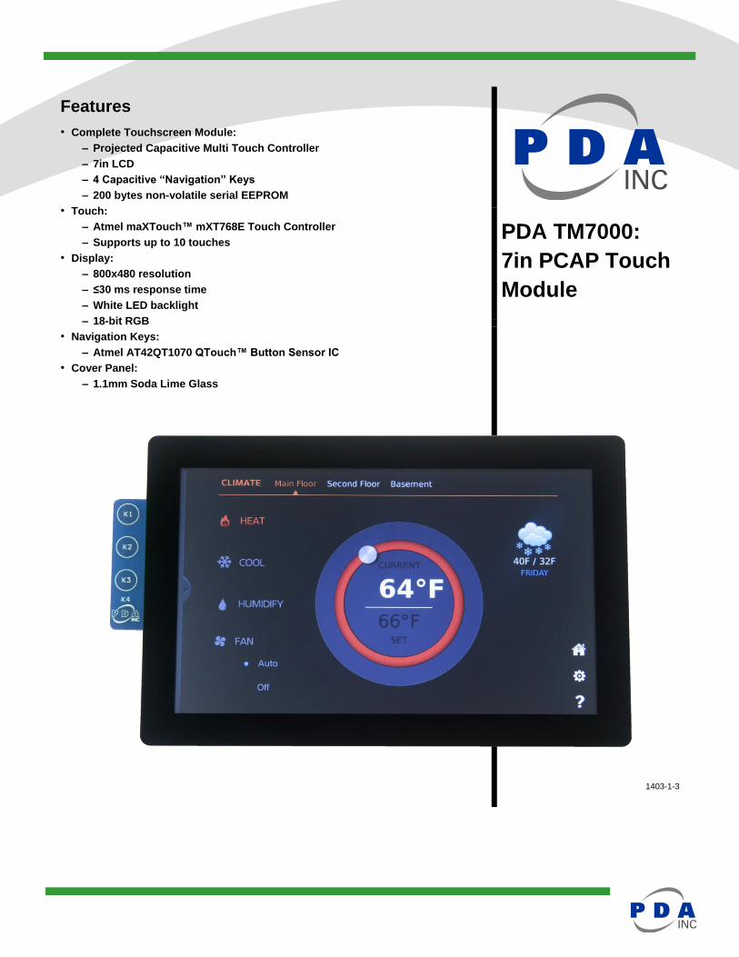
Features
• Complete Touchscreen Module:
– Projected Capacitive Multi Touch Controller
– 7in LCD
– 4 Capacitive “Navigation” Keys
– 200 bytes non-volatile serial EEPROM
• Touch:
– Atmel maXTouch™ mXT768E Touch Controller
– Supports up to 10 touches
• Display:
– 800x480 resolution
– ≤30 ms response time
– White LED backlight
– 18-bit RGB
• Navigation Keys:
– Atmel AT42QT1070 QTouch™ Button Sensor IC
• Cover Panel:
– 1.1mm Soda Lime Glass
PDA TM7000:
7in PCAP Touch
Module
1403-1-3

2 PDA TM7000: 7in PCAP Touch Module 1403-1-3
Contents
1 Module Overview 4
1.1 PCB Connections 4
1.2 Debug Connector J1 5
1.3 LCD Backlight Power J2 5
1.4 Host Connector J4 6
1.5 Host Connector J5 7
1.6 Host Interface (Combined) J6 8
1.7 Display Flex Connector J8 9
1.8 Touch Sensor Flex Connector J7 10
2 Overview of the 7in PCAP Touch Module 11
2.1 Introduction 11
2.2 Understanding Unfamiliar Concepts 12
2.3 LCD Panel 12
2.3.1 Scan Direction Selection 12
2.3.2 RGB Signal Routing 13
2.4 maXTouch Capacitive Touchscreen Controller 14
2.4.1 maXTouch Controller Interface 15
2.5 QTouch Capacitive Button Controller 15
2.5.1 QTouch Controller Interface 15
2.6 Serial EEPROM 15
3 Getting Started 16
3.1 Hardware Connections 16
3.2 Software 16
3.3 Using the Touch Module 16
3.3.1 Navigation Keys 16
3.3.2 Evaluating the Touch Module 17
4 Specifications 18
4.1 Mechanical Specifications 18
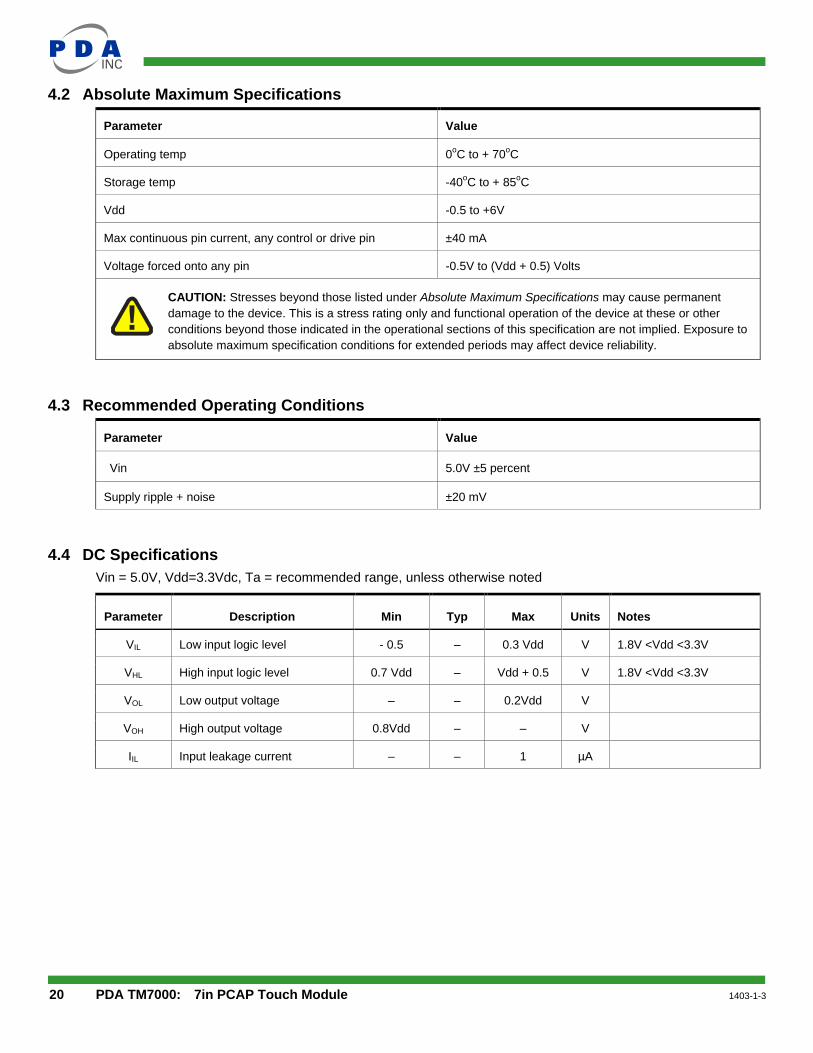
4.2 Absolute Maximum Specifications 20
4.3 Recommended Operating Conditions 20
4.4 DC Specifications 20
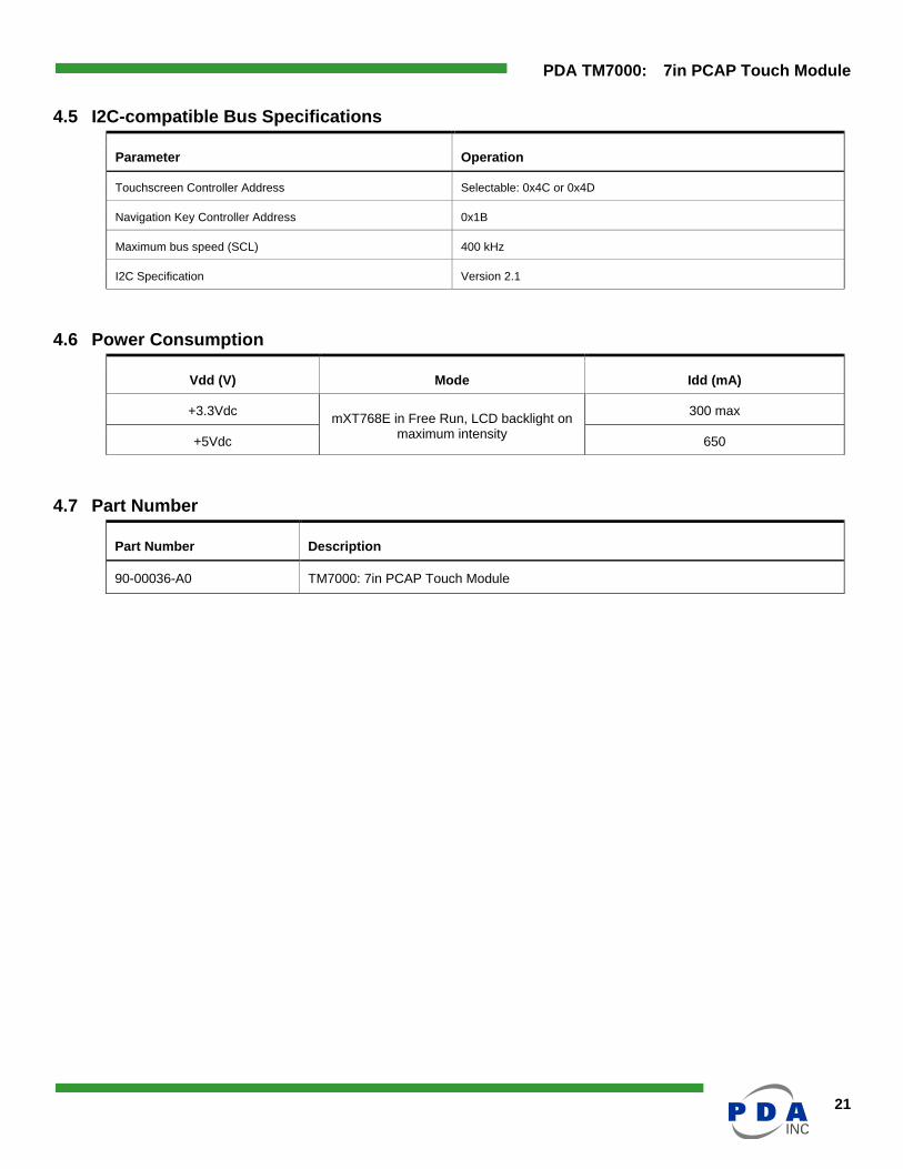
4.5 I2C-compatible Bus Specifications 21
4.6 Power Consumption 21
4.7 Part Number 21
5 I2C Basics (I2C-compatible Operation) 22

PDA TM7000: 7in PCAP Touch Module
3
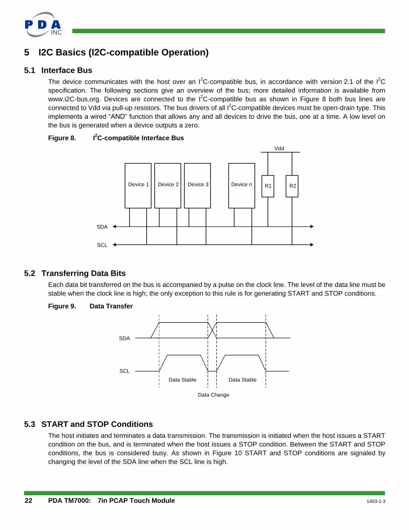
5.1 Interface Bus 22
5.2 Transferring Data Bits 22
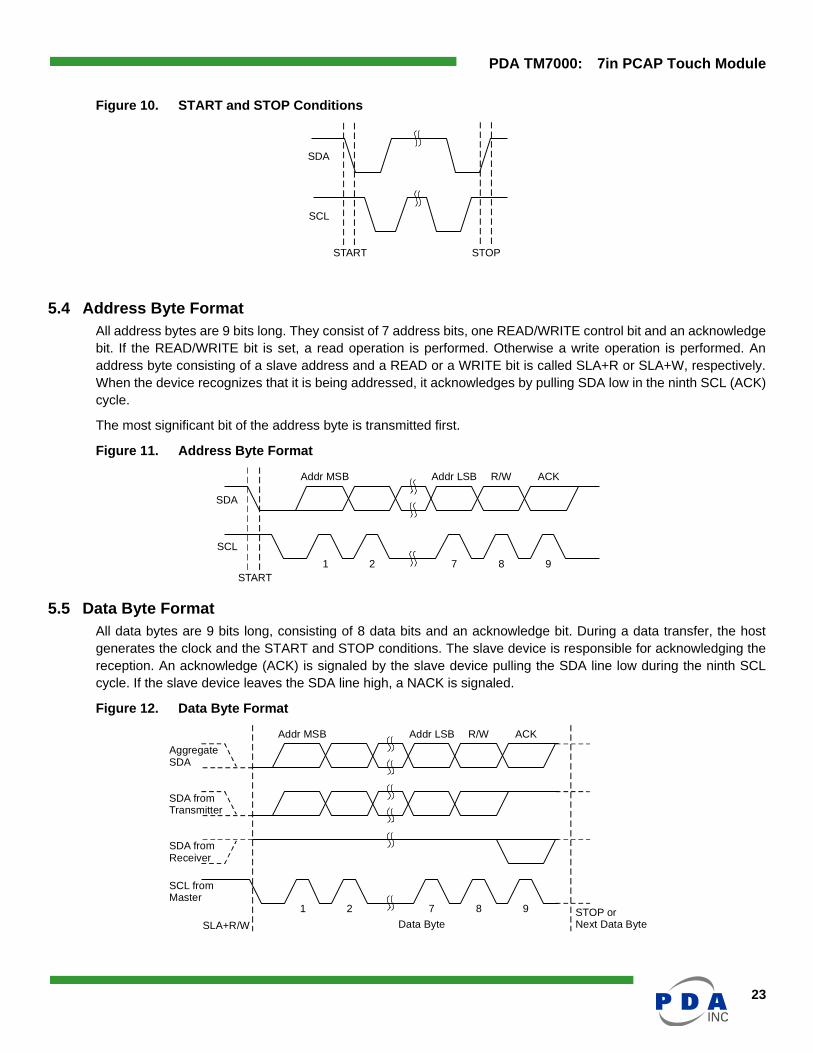
5.3 START and STOP Conditions 22
5.4 Address Byte Format 23
5.5 Data Byte Format 23
5.6 Combining Address and Data Bytes into a Transmission 24
6 Revision History 25
7 Notes 26

4 PDA TM7000: 7in PCAP Touch Module 1403-1-3
1 Module Overview
1.1 PCB Connections
Figure 1 - PCB Connectors
NOTE: Connector J7 is on the bottom side of the PCB.
The following notations are used for pin descriptions:
I Input only OD Open drain output
O Output only, push-pull P Ground or power
MXT maXTouch touchscreen QT QTouch Button Controller
EE Serial EEPROM LCD LCD Panel
NOTE: Inputs and output are defined from the standpoint of the Touch Module.
MXT768E
DS
24
B3
3
J4
J1 J2
J7
J4
J6
TouchSensor Flex
Ho
st
Debug LCD Power
Ho
st
CombinedHost
J8Display Flex
Pin 1
Pin 1
Pin 1
Pin
1
Pin 1
Pin 1

PDA TM7000: 7in PCAP Touch Module
5
1.2 Debug Connector J1
Connector J1 carries signals used to debug the MaXTouch Touch Controller and QTouch Button Controller.
Pin Type Description MX
T
QT
Pin Type Description MX
T
QT
1 P +5Vdc 6 I/O I2C SCL
2 O ~QT_CHG 7 - N/C
3 O ~MXT_CHG 8 P GND
4 - N/C 9 O DBG DATA
5 I I2C SDA 10 O DBG CLK
1.3 LCD Backlight Power J2
Connector J2 is used to provide +5Vdc system and LCD backlight power to the touch module when the Connector
J6 host interface is being used. The host interface on connector J6 only provides +3.3Vdc system power. By
contrast, when the TM7000 is connected to the host via connectors J4 and J5, system power and LCD backlight
power is provided through those interfaces.
NOTE: J2 should NOT be used when J4 and J5 are in use.
The mating connector for J2 is a 2.1mm I.D x 5.5mm O.D barrel connector (center positive). A +5Vdc supply
rated for 1A minimum should connected to J2.
Suggested power supplies:
- Phihong PSC12R-050, (+5Vdc, 2A)
- Phihong PSAC05R-050(P), (+5Vdc, 1A)

6 PDA TM7000: 7in PCAP Touch Module 1403-1-3
1.4 Host Connector J4
Connector J4 connects to the host and carries signals between the host and (1) the MaXTouch Touch Controller,
(2) the QTouch Button Controller and (3) LCD Panel.
NOTE: J4 (and J5) should not be used when J6 is in use.
J2 should not be used when J4 (and J5) are in use.
Pin Type Description MX
T
LC
D
QT
EE
Pin Type Description MX
T
LC
D
QT
EE
1 P +3.3Vdc 16 I LCD_DATA_12
2 P GND 17 P GND
3 P +3.3Vdc 18 I LCD_DATA_0
4 P GND 19 I LCD_DATA_1
5 O ~MXT_CHG 20 I LCD_DATA_2
6 O ~QT_CHG 21 I LCD_DATA_3
7 I I2C SCL 22 I LCD_DATA_4
8 I/O I2C SDA 23 I LCD_DATA_5
9 P GND 24 I LCD_DATA_6
10 I LCD_DATA_15 25 I LCD_DATA_7
11 P GND 26 I LCD_DATA_8
12 I LCD_DATA_13 27 I LCD_DATA_9
13 P GND 28 I LCD_DATA_10
14 I LCD_DATA_14 29 I LCD_DATA_11
15 P GND 30 P GND

PDA TM7000: 7in PCAP Touch Module
7
1.5 Host Connector J5
Connector J5 connects to the host and carries signals between the host and (1) the LCD Panel and (2) serial
EEPROM.
NOTE: J5 (and J4) should not be used when J6 is in use.
J2 should not be used when J5 (and J4) are in use.
Pin Type Description MX
T
LC
D
QT
EE
Pin Type Description MX
T
LC
D
QT
EE
1 P +5Vdc 21 P GND
2 P GND 22 P GND
3 P +5Vdc 23 - N/C
4 P GND 24 - N/C
5 I LCD_DATA_16 25 - N/C
6 I LCD_DATA_17 26 - N/C
7 I LCD_DATA_18 27 - N/C
8 I LCD_DATA_19 28 I/O One-Wire Interface
9 I LCD_DATA_20 29 P GND
10 I LCD_DATA_21 30 P GND
11 I LCD_DATA_22 31 - N/C
12 I LCD_DATA_23 32 - N/C
13 P GND 33 - N/C
14 P GND 34 - N/C
15 I DISP (Display Enable) 35 - N/C
16 I Backlight PWM 36 O Module Presence Detect
17 I VSYNC 37 - N/C – See Note 1
18 I HSYNC 38 - N/C
19 I DE 39 P GND
20 I PCLK 40 P GND
Note 1: by populating R5, the touch module’s ~RESET signal is accessible at this pin.

8 PDA TM7000: 7in PCAP Touch Module 1403-1-3
1.6 Host Interface (Combined) J6
Connector J6 connects to the host and carries the combined signals of J4 and J5. It provides an alternate
interface between the host and (1) the MaXTouch Touch Controller, (2) the QTouch Button Controller, (3) LCD
Panel, and (4) serial EEPROM.
When the host interface on connector J6 is used, +5Vdc system power must be provided using Connector J2. See
Section 1.3 for details.
NOTE: J6 should not be used when J4 and J5 are in use.
Pin Type Description MX
T
LC
D
QT
EE
Pin Type Description MX
T
LC
D
QT
EE
1 I/O One-Wire Interface 26 I LCD_DATA_19
2 P GND 27 P GND
3 I LCD_DATA_0 28 I LCD_DATA_20
4 I LCD_DATA_1 29 I LCD_DATA_21
5 I LCD_DATA_2 30 I LCD_DATA_22
6 I LCD_DATA_3 31 I LCD_DATA_23
7 P GND 32 P GND
8 I LCD_DATA_4 33 I PCLK
9 I LCD_DATA_5 34 I VSYNC
10 I LCD_DATA_6 35 I HSYNC
11 I LCD_DATA_7 36 I DE
12 P GND 37 - N/C
13 I LCD_DATA_8 38 - N/C
14 I LCD_DATA_9 39 - N/C
15 I LCD_DATA_10 40 - N/C
16 I LCD_DATA_11 41 I DISP
17 P GND 42 I I2C SDA
18 I LCD_DATA_12 43 I/O I2C SCL
19 I LCD_DATA_13 44 O ~MXT_CHG
20 I LCD_DATA_14 45 O ~QT_CHG
21 I LCD_DATA_15 46 I LCD_PWM
22 P GND 47 I ~RESET
23 I LCD_DATA_16 48 P +3.3Vdc
24 I LCD_DATA_17 49 P +3.3Vdc
25 I LCD_DATA_18 50 P GND
PDA TM7000: 7in PCAP Touch Module
9
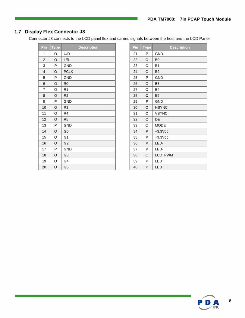
1.7 Display Flex Connector J8
Connector J8 connects to the LCD panel flex and carries signals between the host and the LCD Panel.
Pin Type Description Pin Type Description
1 O U/D 21 P GND
2 O L/R 22 O B0
3 P GND 23 O B1
4 O PCLK 24 O B2
5 P GND 25 P GND
6 O R0 26 O B3
7 O R1 27 O B4
8 O R2 28 O B5
9 P GND 29 P GND
10 O R3 30 O HSYNC
11 O R4 31 O VSYNC
12 O R5 32 O DE
13 P GND 33 O MODE
14 O G0 34 P +3.3Vdc
15 O G1 35 P +3.3Vdc
16 O G2 36 P LED-
17 P GND 37 P LED-
18 O G3 38 O LCD_PWM
19 O G4 39 P LED+
20 O G5 40 P LED+

10 PDA TM7000: 7in PCAP Touch Module 1403-1-3
1.8 Touch Sensor Flex Connector J7
Connector J7 connects to the touch sensor flex and carries signals used by the maXTouch controller to detect user
input on the touch sensor.
Pin Type Description Pin Type Description
1 P GND 29 I/O Y7
2 I/O X0 30 I/O Y8
3 I/O X1 31 I/O Y9
4 I/O X2 32 I/O Y10
5 I/O X3 33 I/O Y11
6 I/O X4 34 I/O Y12
7 I/O X5 35 I/O Y13
8 I/O X6 36 I/O Y14
9 I/O X7 37 I/O Y15
10 I/O X8 38 I/O Y16
11 I/O X9 39 I/O Y17
12 I/O X10 40 I/O Y18
13 I/O X11 41 I/O Y19
14 I/O X12 42 I/O Y20
15 I/O X13 43 I/O Y21
16 I/O X14 44 I/O Y22
17 I/O X15 45 I/O Y23
18 I/O X16 46 I/O Y24
19 I/O X17 47 I/O Y25
20 I/O X18 48 I/O Y26
21 P GND 49 I/O Y27
22 I/O Y0 50 I/O Y28
23 I/O Y1 51 I/O Y29
24 I/O Y2 52 I/O Y30
25 I/O Y3 53 I/O Y31
26 I/O Y4 54 P GND
27 I/O Y5 55 P GND
28 I/O Y6
PDA TM7000: 7in PCAP Touch Module
11
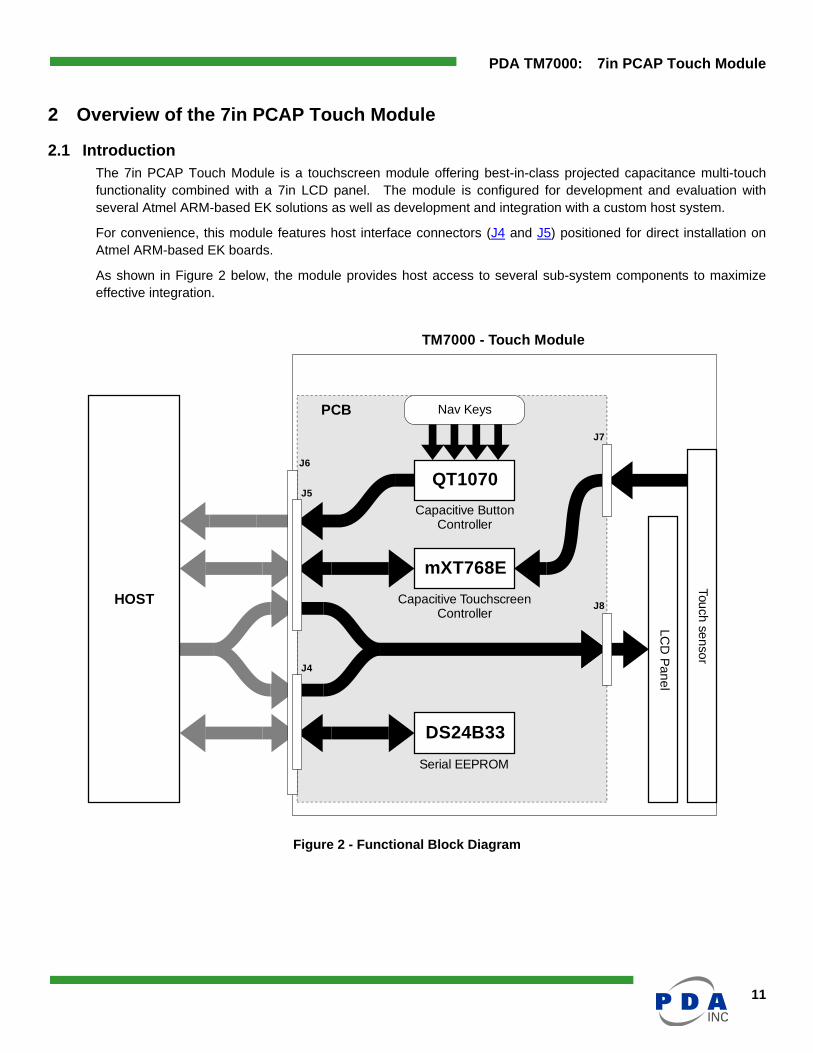
2 Overview of the 7in PCAP Touch Module
2.1 Introduction
The 7in PCAP Touch Module is a touchscreen module offering best-in-class projected capacitance multi-touch
functionality combined with a 7in LCD panel. The module is configured for development and evaluation with
several Atmel ARM-based EK solutions as well as development and integration with a custom host system.
For convenience, this module features host interface connectors (J4 and J5) positioned for direct installation on
Atmel ARM-based EK boards.
As shown in Figure 2 below, the module provides host access to several sub-system components to maximize
effective integration.
Figure 2 - Functional Block Diagram
HOST
Tou
ch
se
nso
r
LC
D P
an
el
TM7000 - Touch Module
QT1070
Nav Keys
mXT768E
DS24B33
Capacitive ButtonController
Capacitive TouchscreenController
Serial EEPROM
PCB
J5
J4
J7
J8
J6
12 PDA TM7000: 7in PCAP Touch Module 1403-1-3
2.2 Understanding Unfamiliar Concepts
Throughout this document, the functionality of the module sub-system will be outlined and summarized. However,
the user is encouraged to refer to the resources and documents below in order to gain a more thorough
understanding of each sub-system.
• For a basic overview of I2C communication, refer to Section 5 of this document
• Atmel maXTouch mXT768E Datasheet (www.atmel.com)
• Atmel QTouch QT1070 Datasheet (www.atmel.com)
• Maxim DS24B33 Datasheet (www.maximintegrated.com)
In addition, when developing or evaluating with the Atmel ARM-based EK’s, it is recommended that the user visit
www.at91.com which contains a broad range of resources for the EK’s and the ARM devices they feature.
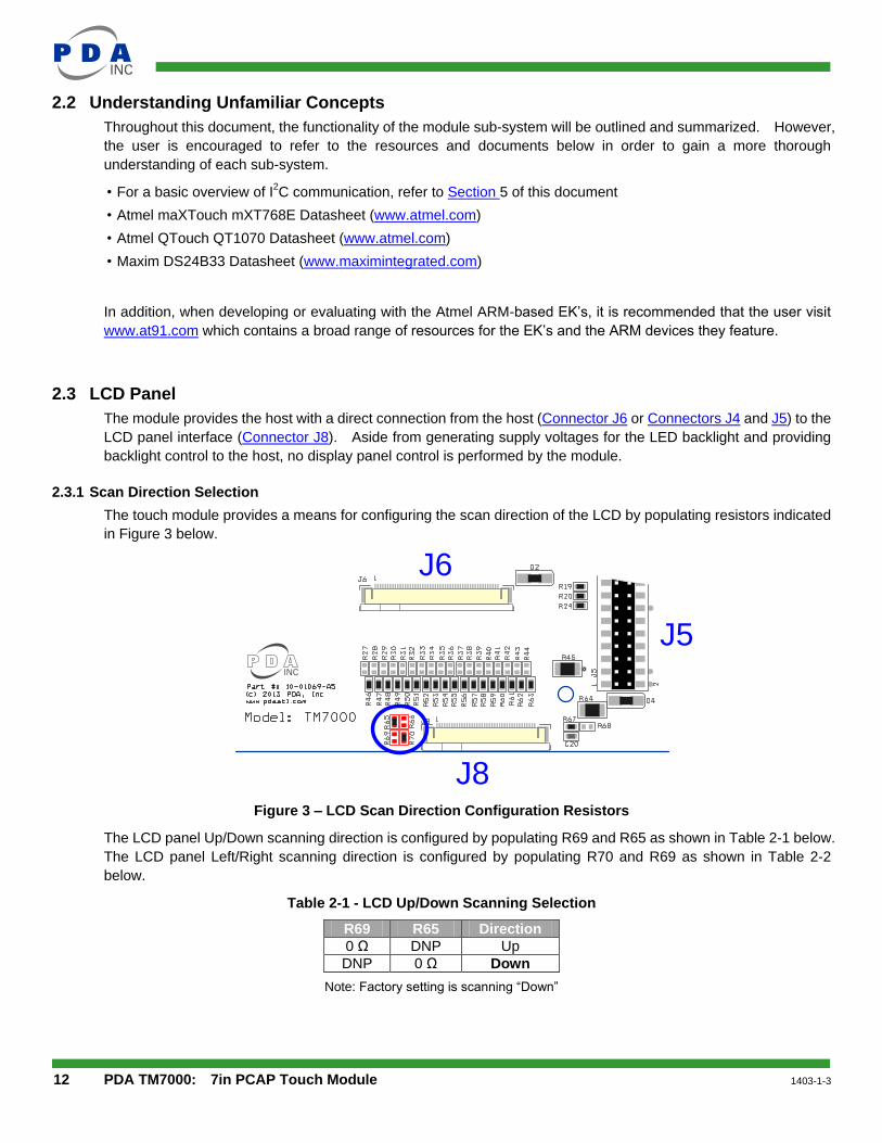
2.3 LCD Panel
The module provides the host with a direct connection from the host (Connector J6 or Connectors J4 and J5) to the
LCD panel interface (Connector J8). Aside from generating supply voltages for the LED backlight and providing
backlight control to the host, no display panel control is performed by the module.
2.3.1 Scan Direction Selection
The touch module provides a means for configuring the scan direction of the LCD by populating resistors indicated
in Figure 3 below.
Figure 3 – LCD Scan Direction Configuration Resistors
The LCD panel Up/Down scanning direction is configured by populating R69 and R65 as shown in Table 2-1 below.
The LCD panel Left/Right scanning direction is configured by populating R70 and R69 as shown in Table 2-2
below.
Table 2-1 - LCD Up/Down Scanning Selection
R69 R65 Direction
0 Ω DNP Up
DNP 0 Ω Down
Note: Factory setting is scanning “Down”
J8
J6
J5
PDA TM7000: 7in PCAP Touch Module
13
Table 2-2 - LCD Left/Right Scanning Selection
R70 R66 Direction
0 Ω DNP Right
DNP 0 Ω Left
Note: Factory setting is scanning “Right”
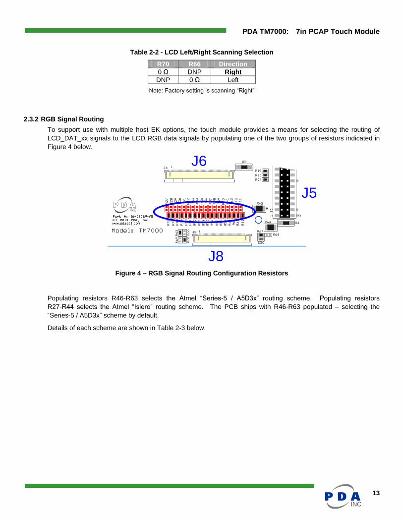
2.3.2 RGB Signal Routing
To support use with multiple host EK options, the touch module provides a means for selecting the routing of
LCD_DAT_xx signals to the LCD RGB data signals by populating one of the two groups of resistors indicated in
Figure 4 below.
Figure 4 – RGB Signal Routing Configuration Resistors
Populating resistors R46-R63 selects the Atmel “Series-5 / A5D3x” routing scheme. Populating resistors
R27-R44 selects the Atmel “Islero” routing scheme. The PCB ships with R46-R63 populated – selecting the
“Series-5 / A5D3x” scheme by default.
Details of each scheme are shown in Table 2-3 below.
J8
J6
J5
14 PDA TM7000: 7in PCAP Touch Module 1403-1-3
Table 2-3 – RGB Signal Routing Selection
Series 5/A5D3x (R46 – R63)
Islero (R27 - R44)
LCM
LCD_DAT_17 LCD_DAT_23 R5
LCD_DAT_16 LCD_DAT_22 R4
LCD_DAT_15 LCD_DAT_21 R3
LCD_DAT_14 LCD_DAT_20 R2
LCD_DAT_13 LCD_DAT_19 R1
LCD_DAT_12 LCD_DAT_18 R0
LCD_DAT_11 LCD_DAT_15 G5
LCD_DAT_10 LCD_DAT_14 G4
LCD_DAT_9 LCD_DAT_13 G3
LCD_DAT_8 LCD_DAT_12 G2
LCD_DAT_7 LCD_DAT_11 G1
LCD_DAT_6 LCD_DAT_10 G0
LCD_DAT_5 LCD_DAT_7 B5
LCD_DAT_4 LCD_DAT_6 B4
LCD_DAT_3 LCD_DAT_5 B3
LCD_DAT_2 LCD_DAT_4 B2
LCD_DAT_1 LCD_DAT_3 B1
LCD_DAT_0 LCD_DAT_2 B0
Note: Factory setting is “Series 5/A5D3x”
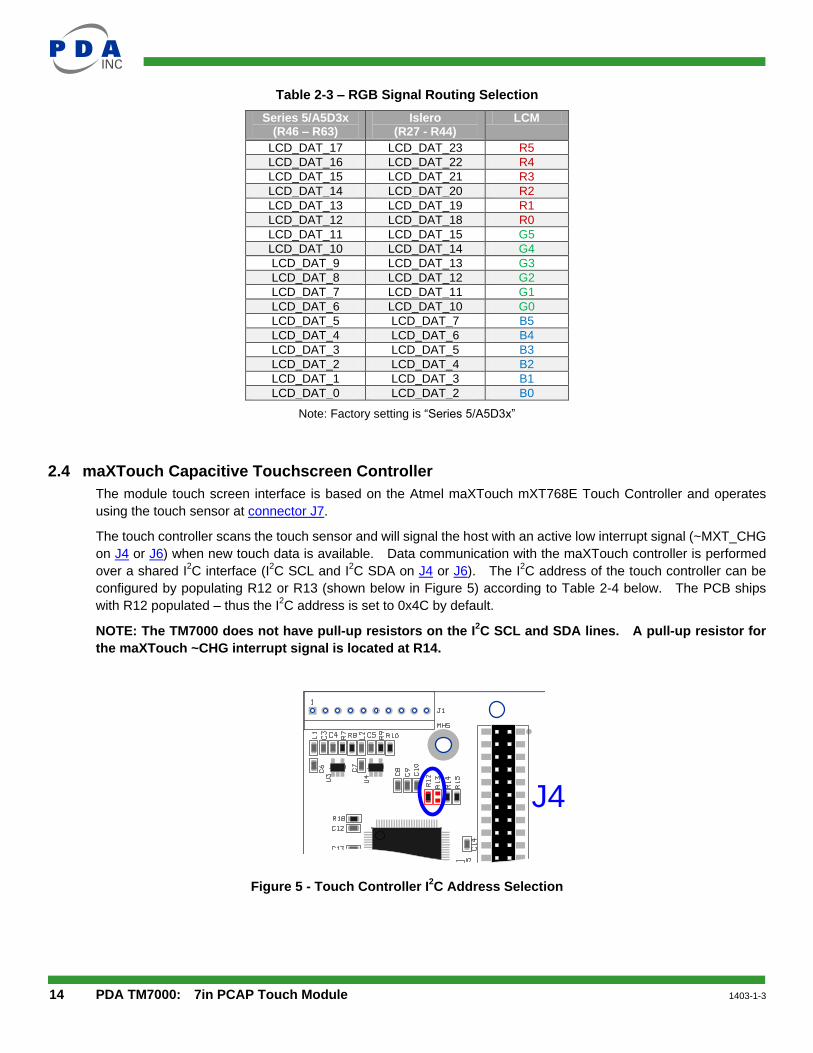
2.4 maXTouch Capacitive Touchscreen Controller
The module touch screen interface is based on the Atmel maXTouch mXT768E Touch Controller and operates
using the touch sensor at connector J7.
The touch controller scans the touch sensor and will signal the host with an active low interrupt signal (~MXT_CHG
on J4 or J6) when new touch data is available. Data communication with the maXTouch controller is performed
over a shared I2C interface (I
2C SCL and I
2C SDA on J4 or J6). The I
2C address of the touch controller can be
configured by populating R12 or R13 (shown below in Figure 5) according to Table 2-4 below. The PCB ships
with R12 populated – thus the I2C address is set to 0x4C by default.
NOTE: The TM7000 does not have pull-up resistors on the I2C SCL and SDA lines. A pull-up resistor for
the maXTouch ~CHG interrupt signal is located at R14.
Figure 5 - Touch Controller I2C Address Selection
J4
PDA TM7000: 7in PCAP Touch Module
15
Table 2-4 - Touch Controller I2C Address Selection
R12 R13 I2C Address
0 Ω DNP 0x4C
DNP 0 Ω 0x4D
Note: 0x4C is the default I2C address
2.4.1 maXTouch Controller Interface
Details of the maXTouch communication protocol are beyond the scope of this document. However information is
provided in Section 3.2 below to facilitate evaluation and initial development.
This module is pre-loaded with a configuration already optimized for this touch sensor and panel, so the
developer need only focus on interfacing with the device. When developing the maXTouch controller
interface during evaluation and host development, care should be taken to avoid changing the maXTouch
configuration or committing changes to NV storage on the maXTouch controller.
To get started with host interface development, the user is strongly encouraged to leverage existing code available
from the resources outlined in Sections 3.2.
2.5 QTouch Capacitive Button Controller
The module’s “nav key” interface is based on the Atmel QT1070 7-Channel Capacitive Sensor Driver.
The button controller scans the 4 capacitive nav keys (K1, K2, K3 and K4) and will signal the host with an active
low interrupt signal (~QT_CHG on Connector J4 or J6) when a touch event has occurred. Data communication
with the QT1070 controller is performed over a shared I2C interface (I
2C SCL and I
2C SDA on J4 or J6). The I
2C
address of the button controller is 0x1B and cannot be changed.
NOTE: The TM7000 does not have pull-up resistors on the I2C SCL and SDA lines. A pull-up resistor for
the QTouch ~CHG interrupt signal is located at R16.
2.5.1 QTouch Controller Interface
Details of the QTouch communication protocol are beyond the scope of this document. The user is encouraged
to review the QT1070 Datasheet (www.atmel.com).
2.6 Serial EEPROM
The module includes a DS24B33 Serial EEPROM providing 512 bytes of non-volatile storage. Data
communication with the EEPROM is performed over a One-Wire Interface. The EEPROM is not used by another
subsystem on the touch module and can be freely used by the host system for any purpose. For example, Atmel
ARM-based EK’s running Linux or Android operating systems use the pre-programmed contents of the EEPROM
to identify this module type.
NOTE: The user should take care if choosing to overwrite the pre-programmed EEPROM contents. As
noted above, certain builds of Linux or Android targeted for the Atmel ARM-based EKs use the EEPROM
contents to identify the module and may no longer recognize the module. The user is advised to backup
the EEPROM contents before overwriting.
The serial EEPROM communicates via a one-wire interface (One-wire Interface on J5 or J6). Refer to the
DS24B33 Datasheet (www.maximintegrated.com) for details.

16 PDA TM7000: 7in PCAP Touch Module 1403-1-3
3 Getting Started
This module was designed to install on a variety of Atmel ARM-based EK’s including the SAM9X5-EK,
SAM9N12-EK, SAMA5D3x-EK and the SAMA5D3 Xplained. This provides the fastest way to evaluate the
performance of the touchscreen and display using a familiar, full-featured OS.
The following sections provide basic information related to using and evaluating the Touch Module. Visit
Precision Design Associates website ( www.pdaatl.com ) or Atmel’s AT91 Community website ( www.at91.com )
for more information related to this touch module or guidance appropriate for your specific EK.
3.1 Hardware Connections
The module interfaces with the EK board via one of two methods depending on the EK:
the two large dual-row headers, J4 and J5
the flex connector, J6
Refer to the specific EK documentation to determine which method is appropriate.
3.2 Software
Several options exist when developing for the touch module whether targeting a custom host or an Atmel EK.
3.2.1.1 Atmel Software Framework
The Atmel Software Framework (asf.atmel.com) contains examples of code for interfacing with devices in the
maXTouch family of touch controllers. The capabilities of various maXTouch devices may differ, but the basic
communication protocol is common and can be applied to this module.
3.2.1.2 Linux Kernel / Android
The Linux Kernel (www.kernel.org) has included basic support for maXTouch touch devices since version 2.6.36.
The mainline driver has undergone considerable evolution since then.
Atmel hosts the AT91 community website with resources dedicated to developing their EKs for Android
( www.at91.com/android4sam/ ) and Linux ( www.at91.com/linux4sam/ )
In addition, Atmel maintains patches (www.github.com/atmel-maxtouch/linux) which provide numerous out-of-cycle
improvements to the mainline Linux Kernel driver.
3.3 Using the Touch Module
3.3.1 Navigation Keys
When using this module with one of the standard Atmel Android demo builds, the navigation keys function as
shown in Table 3-1 below:
PDA TM7000: 7in PCAP Touch Module
17
Table 3-1 - Navigation Key Function (Android)
Key Navigation Function
K1 Back
K2 Menu
K3 Home
K4 Power / Sleep
3.3.2 Evaluating the Touch Module
For effective evaluation of the module – the touch sensor and the LCD panel in particular – the user is encouraged to try
the following applications and tools depending on the host OS.
3.3.2.1 Android
The following Android apps available from Google Play:
TouchTest by Moonblink
Dotty by Gerry Steele
Multitouch Visible Test by Battery Powered Games
Screen Test by Amberfog
3.3.2.2 Linux
The user can perform simple touch / drawing test using the ts_test utility that is part of tslib.

18 PDA TM7000: 7in PCAP Touch Module 1403-1-3
4 Specifications
For complete specifications, refer to the datasheets listed in section 2.2 for the various sub-system components
outlined in sections 2.3 through 2.6.
4.1 Mechanical Specifications
Drawings and CAD models available upon request.
Figure 6 - Sensor Only Dimensions
Sensor Assy (P/N: 90-00020-A0) may be purchased individually.
Minimum order quantities apply. Contact PDA for details.
1.1 mm(Cover Panel)
0.45 mm (Sensor+ Optically ClearAdhesive)
0.08 mm(FPC)
X18,Y0
X0,Y0
X18,Y31
X0,Y31
10
7.0
2(
Ou
tline
)S
ub
stra
te
±0
.15
mm
166.55( Outline)Substrate
±0.15mm
54
.7 m
m(S
en
so
r S
ub
str
ate
to F
PC
Ed
ge)
50.4 mm(FPC Max Width)
28 mm(FPC Min Width)
NOTE: PCB Contactsface DOWN as drawn
PIN
1
12 m
m(C
over P
ane
l Ed
ge
to B
ackprin
t Vie
wa
ble
)
12 mm(Cover Panel Edgeto Backprint Viewable)
154 mm(Backprint Viewable)
93
mm
(Bac
kp
rint V
iew
ab
le)
152.4 mm(LCD Active)
91
.44
mm
(LC
D A
ctiv
e)
Glass Profile178mm x 117mm
R3.75mm in corners
PIN
55
Viewed fromuser side
Use
r sid
e
LC
D s
ide

PDA TM7000: 7in PCAP Touch Module
19
Figure 7 – Module Dimensions
MXT768E
DS
24
B3
3
50 m
m
63
.5 m
m(P
CB
Wid
th)
134.6 mm(PCB Length)
22 mm
Glass Profile178mm x 117mm
R3.75mm in corners
9.3 mm(Cover Panel rear surface
to PCB rear surface)
104 m
m(L
CM
Fra
me W
idth
)
104 mm(LCM Frame Length)
6.6 mm(Cover Panel rear surface
to LCM rear surface)
13.5
mm
20 PDA TM7000: 7in PCAP Touch Module 1403-1-3
4.2 Absolute Maximum Specifications
Parameter Value
Operating temp 0oC to + 70
oC
Storage temp -40oC to + 85
oC
Vdd -0.5 to +6V
Max continuous pin current, any control or drive pin ±40 mA
Voltage forced onto any pin -0.5V to (Vdd + 0.5) Volts
CAUTION: Stresses beyond those listed under Absolute Maximum Specifications may cause permanent
damage to the device. This is a stress rating only and functional operation of the device at these or other
conditions beyond those indicated in the operational sections of this specification are not implied. Exposure to
absolute maximum specification conditions for extended periods may affect device reliability.
4.3 Recommended Operating Conditions
Parameter Value
Vin 5.0V ±5 percent
Supply ripple + noise ±20 mV
4.4 DC Specifications
Vin = 5.0V, Vdd=3.3Vdc, Ta = recommended range, unless otherwise noted
Parameter Description Min Typ Max Units Notes
VIL Low input logic level - 0.5 – 0.3 Vdd V 1.8V <Vdd <3.3V
VHL High input logic level 0.7 Vdd – Vdd + 0.5 V 1.8V <Vdd <3.3V
VOL Low output voltage – – 0.2Vdd V
VOH High output voltage 0.8Vdd – – V
IIL Input leakage current – – 1 µA
PDA TM7000: 7in PCAP Touch Module
21
4.5 I2C-compatible Bus Specifications
Parameter Operation
Touchscreen Controller Address Selectable: 0x4C or 0x4D
Navigation Key Controller Address 0x1B
Maximum bus speed (SCL) 400 kHz
I2C Specification Version 2.1
4.6 Power Consumption
Vdd (V) Mode Idd (mA)
+3.3Vdc mXT768E in Free Run, LCD backlight on
maximum intensity
300 max
+5Vdc 650
4.7 Part Number
Part Number Description
90-00036-A0 TM7000: 7in PCAP Touch Module
22 PDA TM7000: 7in PCAP Touch Module 1403-1-3
5 I2C Basics (I2C-compatible Operation)
5.1 Interface Bus
The device communicates with the host over an I2C-compatible bus, in accordance with version 2.1 of the I
2C
specification. The following sections give an overview of the bus; more detailed information is available from
www.i2C-bus.org. Devices are connected to the I2C-compatible bus as shown in Figure 8 both bus lines are
connected to Vdd via pull-up resistors. The bus drivers of all I2C-compatible devices must be open-drain type. This
implements a wired “AND” function that allows any and all devices to drive the bus, one at a time. A low level on
the bus is generated when a device outputs a zero.
Figure 8. I2C-compatible Interface Bus
5.2 Transferring Data Bits
Each data bit transferred on the bus is accompanied by a pulse on the clock line. The level of the data line must be
stable when the clock line is high; the only exception to this rule is for generating START and STOP conditions.
Figure 9. Data Transfer
5.3 START and STOP Conditions
The host initiates and terminates a data transmission. The transmission is initiated when the host issues a START
condition on the bus, and is terminated when the host issues a STOP condition. Between the START and STOP
conditions, the bus is considered busy. As shown in Figure 10 START and STOP conditions are signaled by
changing the level of the SDA line when the SCL line is high.
SDA
SCL
Device 1 Device 2 Device 3 Device n
Vdd
R1 R2
SDA
SCL
Data Stable Data Stable
Data Change
PDA TM7000: 7in PCAP Touch Module
23
Figure 10. START and STOP Conditions
5.4 Address Byte Format
All address bytes are 9 bits long. They consist of 7 address bits, one READ/WRITE control bit and an acknowledge
bit. If the READ/WRITE bit is set, a read operation is performed. Otherwise a write operation is performed. An
address byte consisting of a slave address and a READ or a WRITE bit is called SLA+R or SLA+W, respectively.
When the device recognizes that it is being addressed, it acknowledges by pulling SDA low in the ninth SCL (ACK)
cycle.
The most significant bit of the address byte is transmitted first.
Figure 11. Address Byte Format
5.5 Data Byte Format
All data bytes are 9 bits long, consisting of 8 data bits and an acknowledge bit. During a data transfer, the host
generates the clock and the START and STOP conditions. The slave device is responsible for acknowledging the
reception. An acknowledge (ACK) is signaled by the slave device pulling the SDA line low during the ninth SCL
cycle. If the slave device leaves the SDA line high, a NACK is signaled.
Figure 12. Data Byte Format
SDA
SCL
START STOP
SDA
SCL
START
1 2 7 8 9
R/WAddr LSB ACKAddr MSB
SLA+R/W
1 2 7 8 9
R/WAddr LSB ACKAddr MSB
AggregateSDA
SDA fromTransmitter
SDA fromReceiver
SCL fromMaster
STOP orNext Data ByteData Byte

24 PDA TM7000: 7in PCAP Touch Module 1403-1-3
5.6 Combining Address and Data Bytes into a Transmission
A transmission consists of a START condition, an SLA+R or SLA+W, one or more data bytes and a STOP
condition. The wired “ANDing” of the SCL line is used to implement handshaking between the host and the device.
The device extends the SCL low period by pulling the SCL line low whenever it needs extra time for processing
between the data transmissions.
Figure 13 shows a typical data transmission. Note that several data bytes can be transmitted between the SLA+R
or SLA+W and the STOP.
Figure 13. Byte Transmission
ACK
1 2 7 8 9Data Byte
SDA
SCL
START
DataLSB
DataMSBR/W
1 2 7 8 9SLA+R/W
AddrLSB
AddrMSB ACK
STOP
PDA TM7000: 7in PCAP Touch Module
25
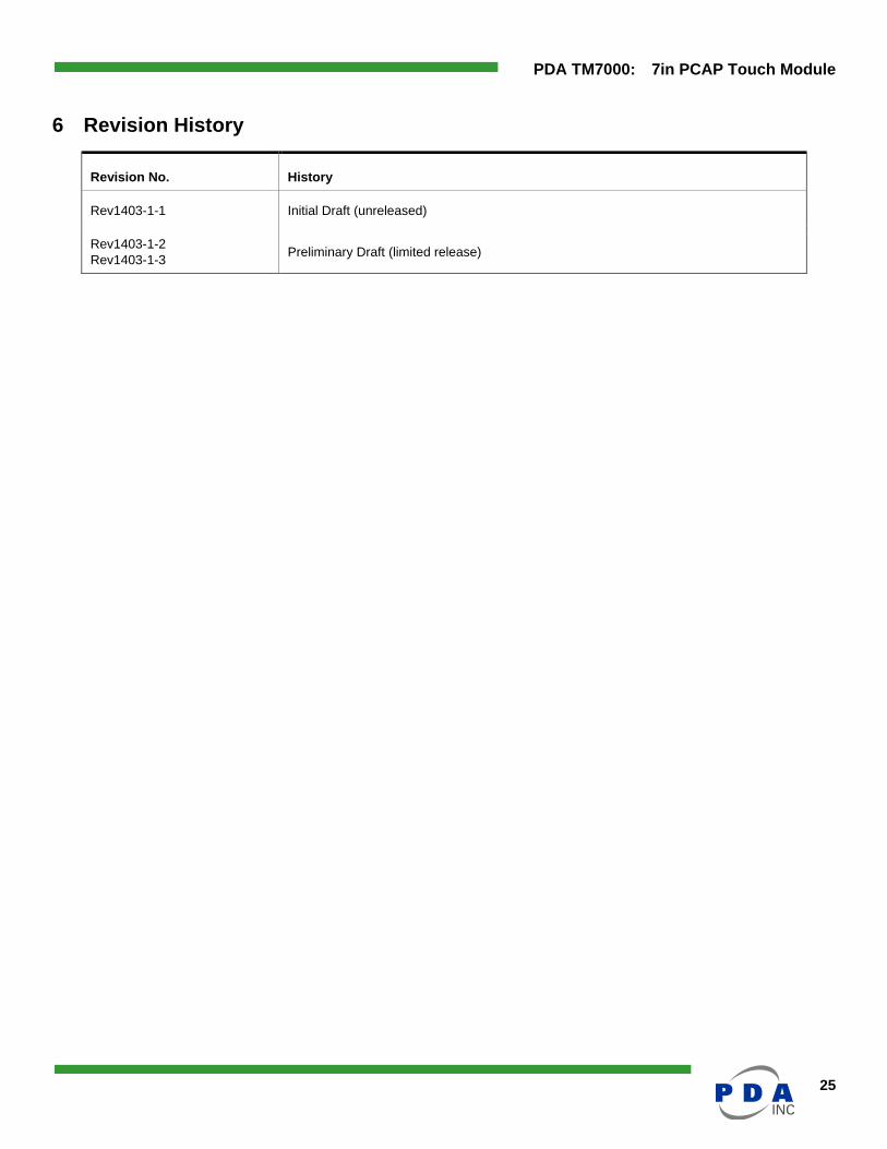
6 Revision History
TM7000 Datasheet - 20140316.docx : 3/16/2014 9:45:00 PM
3/16/2014 9:45 PM Greg Sullivan
Revision No. History
Rev1403-1-1 Initial Draft (unreleased)
Rev1403-1-2
Rev1403-1-3 Preliminary Draft (limited release)
26 PDA TM7000: 7in PCAP Touch Module 1403-1-3
7 Notes
email: [email protected]
Precision Design Associates, Inc. 736 Johnson Ferry Rd, Suite C-270
Marietta, GA 30068
USA
tel: (770)-971-4490
url: http://www.pdaatl.com
© 2014 Precision Design Associates. All rights reserved. Atmel®, Atmel logo and combinations thereof, maXTouch
®, QTouch
®, and others are
registered trademarks of Atmel Corporation or its subsidiaries. Other terms and product names may be registered trademarks or trademarks of others.