72 Mb (2M x 36 & 4M x 18) QUAD (Burst of 4) Synchronous SRAMs · 4 Integrated Silicon Solution,...
29
Integrated Silicon Solution, Inc. 1 Rev. G 11/09/2010 72 Mb (2M x 36 & 4M x 18) QUAD (Burst of 4) Synchronous SRAMs Copyright © 2010 Integrated Silicon Solution, Inc. All rights reserved. ISSI reserves the right to make changes to this specification and its products at any time without notice. ISSI assumes no liability arising out of the application or use of any information, products or services described herein. Customers are advised to obtain the lat- est version of this device specification before relying on any published information and before placing orders for products. November 2010 Features • 2M x 36 or 4M x 18. • On-chip delay-locked loop (DLL) for wide data valid window. • Separate read and write ports with concurrent read and write operations. • Synchronous pipeline read with late write opera- tion. • Double data rate (DDR) interface for read and write input ports. • Fixed 4-bit burst for read and write operations. • Clock stop support. • Two input clocks (K and K ) for address and con- trol registering at rising edges only. • Two input clocks (C and C ) for data output con- trol. • Two echo clocks (CQ and CQ) that are delivered simultaneously with data. • +1.8V core power supply and 1.5, 1.8V V DDQ , used with 0.75, 0.9V V REF . • HSTL input and output levels. • Registered addresses, write and read controls, byte writes, data in, and data outputs. • Full data coherency. • Boundary scan using limited set of JTAG 1149.1 functions. • Byte write capability. • Fine ball grid array (FBGA) package - 15mm x 17mm body size - 1mm pitch - 165-ball (11 x 15) array • Programmable impedance output drivers via 5x user-supplied precision resistor. Description The 72Mb IS61QDB42M36 and IS61QDB44M18 are synchronous, high-perfor- mance CMOS static random access memory (SRAM) devices. These SRAMs have separate I/Os, eliminating the need for high-speed bus turnaround. The rising edge of K clock initiates the read/write operation, and all internal operations are self-timed. Refer to the Timing Reference Diagram for Truth Table on page 8 for a description of the basic opera- tions of these QUAD (Burst of 4) SRAMs. Read and write addresses are registered on alter- nating rising edges of the K clock. Reads and writes are performed in double data rate. The following are registered internally on the rising edge of the K clock: • Read/write address • Read enable • Write enable • Byte writes for burst addresses 1 and 3 • Data-in for burst addresses 1 and 3 The following are registered on the rising edge of the K clock: • Byte writes for burst addresses 2 and 4 • Data-in for burst addresses 2 and 4 Byte writes can change with the corresponding data- in to enable or disable writes on a per-byte basis. An internal write buffer enables the data-ins to be regis- tered one cycle after the write address. The first data-in burst is clocked one cycle later than the write command signal, and the second burst is timed to the following rising edge of the K clock. Two full clock cycles are required to complete a write opera- tion. During the burst read operation, the data-outs from the first and third bursts are updated from output registers off the second and fourth rising edges of the C clock (starting 1.5 cycles later). The data-outs from the second and fourth bursts are updated with the third and fifth rising edges of the C clock. The K and K clocks are used to time the data-outs when- ever the C and C clocks are tied high. Two full clock cycles are required to complete a read operation The device is operated with a single +1.8V power supply and is compatible with HSTL I/O interfaces. • Industrial temperature available
-
Upload
trinhhuong -
Category
Documents
-
view
216 -
download
0
Transcript of 72 Mb (2M x 36 & 4M x 18) QUAD (Burst of 4) Synchronous SRAMs · 4 Integrated Silicon Solution,...

Integrated Silicon Solution, Inc. 1Rev. G11/09/2010
72 Mb (2M x 36 & 4M x 18) QUAD (Burst of 4) Synchronous SRAMs
Copyright © 2010 Integrated Silicon Solution, Inc. All rights reserved. ISSI reserves the right to make changes to this specification and its products at any time without notice. ISSI assumes no liability arising out of the application or use of any information, products or services described herein. Customers are advised to obtain the lat-est version of this device specification before relying on any published information and before placing orders for products.
November 2010
Features• 2M x 36 or 4M x 18.
• On-chip delay-locked loop (DLL) for wide data valid window.
• Separate read and write ports with concurrent read and write operations.
• Synchronous pipeline read with late write opera-tion.
• Double data rate (DDR) interface for read and write input ports.
• Fixed 4-bit burst for read and write operations.
• Clock stop support.
• Two input clocks (K and K) for address and con-trol registering at rising edges only.
• Two input clocks (C and C) for data output con-trol.
• Two echo clocks (CQ and CQ) that are delivered simultaneously with data.
• +1.8V core power supply and 1.5, 1.8V VDDQ, used with 0.75, 0.9V VREF.
• HSTL input and output levels.
• Registered addresses, write and read controls, byte writes, data in, and data outputs.
• Full data coherency.
• Boundary scan using limited set of JTAG 1149.1 functions.
• Byte write capability.
• Fine ball grid array (FBGA) package- 15mm x 17mm body size - 1mm pitch- 165-ball (11 x 15) array
• Programmable impedance output drivers via 5x user-supplied precision resistor.
Description
The 72Mb IS61QDB42M36 and IS61QDB44M18 are synchronous, high-perfor-mance CMOS static random access memory (SRAM) devices. These SRAMs have separate I/Os, eliminating the need for high-speed bus turnaround. The rising edge of K clock initiates the read/write operation, and all internal operations are self-timed. Refer to the Timing Reference Diagram for Truth Table on page 8 for a description of the basic opera-tions of these QUAD (Burst of 4) SRAMs.
Read and write addresses are registered on alter-nating rising edges of the K clock. Reads and writes are performed in double data rate. The following are registered internally on the rising edge of the K clock:
• Read/write address• Read enable• Write enable• Byte writes for burst addresses 1 and 3• Data-in for burst addresses 1 and 3
The following are registered on the rising edge of the K clock:
• Byte writes for burst addresses 2 and 4• Data-in for burst addresses 2 and 4
Byte writes can change with the corresponding data-in to enable or disable writes on a per-byte basis. An internal write buffer enables the data-ins to be regis-tered one cycle after the write address. The first data-in burst is clocked one cycle later than the write command signal, and the second burst is timed to the following rising edge of the K clock. Two full clock cycles are required to complete a write opera-tion.
During the burst read operation, the data-outs from the first and third bursts are updated from output registers off the second and fourth rising edges of the C clock (starting 1.5 cycles later). The data-outs from the second and fourth bursts are updated with the third and fifth rising edges of the C clock. The K and K clocks are used to time the data-outs when-ever the C and C clocks are tied high. Two full clock cycles are required to complete a read operation
The device is operated with a single +1.8V power supply and is compatible with HSTL I/O interfaces.
• Industrial temperature available
2 Integrated Silicon Solution, Inc. Rev. G
11/09/2010
72 Mb (2M x 36 & 4M x 18) QUAD (Burst of 4) Synchronous SRAMs
I
®3Q
x36 FBGA Pinout (Top View)
1 2 3 4 5 6 7 8 9 10 11
A CQ NC/SA* SA W BW2 K BW1 R SA NC/SA* CQ
B Q27 Q18 D18 SA BW3 K BW0 SA D17 Q17 Q8
C D27 Q28 D19 VSS SA NC SA VSS D16 Q7 D8
D D28 D20 Q19 VSS VSS VSS VSS VSS Q16 D15 D7
E Q29 D29 Q20 VDDQ VSS VSS VSS VDDQ Q15 D6 Q6
F Q30 Q21 D21 VDDQ VDD VSS VDD VDDQ D14 Q14 Q5
G D30 D22 Q22 VDDQ VDD VSS VDD VDDQ Q13 D13 D5
H Doff VREF VDDQ VDDQ VDD VSS VDD VDDQ VDDQ VREF ZQ
J D31 Q31 D23 VDDQ VDD VSS VDD VDDQ D12 Q4 D4
K Q32 D32 Q23 VDDQ VDD VSS VDD VDDQ Q12 D3 Q3
L Q33 Q24 D24 VDDQ VSS VSS VSS VDDQ D11 Q11 Q2
M D33 Q34 D25 VSS VSS VSS VSS VSS D10 Q1 D2
N D34 D26 Q25 VSS SA SA SA VSS Q10 D9 D1
P Q35 D35 Q26 SA SA C SA SA Q9 D0 Q0
R TDO TCK SA SA SA C SA SA SA TMS TDI
Note: *The following pins are reserved for higher densities: 10A for 144Mb, and 2A for 288Mb.
x18 FBGA Pinout (Top View)
1 2 3 4 5 6 7 8 9 10 11
A CQ NC/SA* SA W BW1 K NC R SA SA CQ
B NC Q9 D9 SA NC K BW0 SA NC NC Q8
C NC NC D10 VSS SA NC SA VSS NC Q7 D8
D NC D11 Q10 VSS VSS VSS VSS VSS NC NC D7
E NC NC Q11 VDDQ VSS VSS VSS VDDQ NC D6 Q6
F NC Q12 D12 VDDQ VDD VSS VDD VDDQ NC NC Q5
G NC D13 Q13 VDDQ VDD VSS VDD VDDQ NC NC D5
H Doff VREF VDDQ VDDQ VDD VSS VDD VDDQ VDDQ VREF ZQ
J NC NC D14 VDDQ VDD VSS VDD VDDQ NC Q4 D4
K NC NC Q14 VDDQ VDD VSS VDD VDDQ NC D3 Q3
L NC Q15 D15 VDDQ VSS VSS VSS VDDQ NC NC Q2
M NC NC D16 VSS VSS VSS VSS VSS NC Q1 D2
N NC D17 Q16 VSS SA SA SA VSS NC NC D1
P NC NC Q17 SA SA C SA SA NC D0 Q0
R TDO TCK SA SA SA C SA SA SA TMS TDI
Note: *The following pins are reserved for higher densities: 2A for 144Mb.
Integrated Silicon Solution, Inc. 3Rev. G11/09/2010
72 Mb (2M x 36 & 4M x 18) QUAD (Burst of 4) Synchronous SRAMs
Pin Description
Symbol Pin Number Description
K, K 6B, 6A Input clock.
C, C 6P, 6R Input clock for output data control.
CQ, CQ 11A, 1A Output echo clock.
Doff 1H DLL disable when low.
SA 3A, 9A, 4B, 8B, 5C, 7C, 5N, 6N, 7N, 4P, 5P, 7P, 8P, 3R, 4R, 5R, 7R, 8R, 9R 2M x 36 address inputs.
SA 10A, 3A, 9A, 4B, 8B, 5C, 7C, 5N, 6N, 7N, 4P, 5P, 7P, 8P, 3R, 4R, 5R, 7R, 8R, 9R 4M x 18 address inputs.
D0–D8D9–D17D18–D26D27–D35
10P, 11N, 11M, 10K, 11J, 11G, 10E, 11D, 11C10N, 9M, 9L, 9J, 10G, 9F, 10D, 9C, 9B3B, 3C, 2D, 3F, 2G, 3J, 3L, 3M, 2N1C, 1D, 2E, 1G, 1J, 2K, 1M, 1N, 2P
2M x 36 data inputs.
Q0–Q8Q9–Q17Q18–Q26Q27–Q35
11P, 10M, 11L, 11K, 10J, 11F, 11E, 10C, 11B9P, 9N, 10L, 9K, 9G, 10F, 9E, 9D, 10B2B, 3D, 3E, 2F, 3G, 3K, 2L, 3N, 3P1B, 2C, 1E, 1F, 2J, 1K, 1L, 2M, 1P
2M x 36 data outputs.
D0–D8D9–D17
10P, 11N, 11M, 10K, 11J, 11G, 10E, 11D, 11C3B, 3C, 2D, 3F, 2G, 3J, 3L, 3M, 2N
4M x 18 data inputs.
Q0–Q8Q9–Q17
11P, 10M, 11L, 11K, 10J, 11F, 11E, 10C, 11B2B, 3D, 3E, 2F, 3G, 3K, 2L, 3N, 3P
4M x 18 data outputs.
W 4A Write control, active low.
R 8A Read control, active low.
BW0, BW1, BW2, BW3 7B, 7A, 5A,5B 2M x 36 byte write control, active low.
BW0, BW1 7B, 5A 4M x 18 byte write control, active low.
VREF 2H, 10H Input reference level.
VDD 5F, 7F, 5G, 7G, 5H, 7H, 5J, 7J, 5K, 7K Power supply.
VDDQ 4E,8E,4F,8F,4G,8G,3H,4H,8H,9H,4J,8J,4K,8K,4L,8L Output power supply.
VSS4C, 8C, 4D, 5D, 6D, 7D, 8D, 5E, 6E, 7E, 6F, 6G, 6H, 6J, 6K, 5L, 6L, 7L, 4M, 5M, 6M, 7M, 8M, 4N, 8N Ground.
ZQ 11H Output driver impedance control.
TMS, TDI, TCK 10R, 11R, 2R IEEE 1149.1 test inputs (1.8V LVTTL lev-els).
TDO 1R IEEE 1149.1 test output (1.8V LVTTL level).
NC for x36
NC for x18
2A, 10A, 6C
2A, 7A, 1B, 5B, 9B, 10B, 1C, 2C, 6C, 9C, 1D, 9D, 10D, 1E, 2E,9E, 1F, 9F, 10F, 1G, 9G, 10G, 1J, 2J, 9J, 1K, 2K, 9K, 1L, 9L,10L, 1M, 2M, 9M, 1N, 9N, 10N, 1P, 2P, 9P
4 Integrated Silicon Solution, Inc. Rev. G
11/09/2010
72 Mb (2M x 36 & 4M x 18) QUAD (Burst of 4) Synchronous SRAMs
I 3Q
SRAM Features
Read Operations
The SRAM operates continuously in a burst-of-four mode. Read cycles are started by registering R in active low state at the rising edge of the K clock. R can be activated every other cycle because two full cycles are required to complete the burst of four in DDR mode. A second set of clocks, C and C, are used to control the timing to the outputs. A set of free-running echo clocks, CQ and CQ, are produced internally with timings identical to the data-outs. The echo clocks can be used as data capture clocks by the receiver device.
When the C and C clocks are connected high, the K and K clocks assume the function of those clocks. In this case, the data corresponding to the first address is clocked 1.5 cycles later by the rising edge of the K clock. The data corresponding to the second burst is clocked 2 cycles later by the following rising edge of the K clock. The third data-out is clocked by the subsequent rising edge of the K clock, and the fourth data-out is clocked by the subsequent rising edge of the K clock.
A NOP operation (R is high) does not terminate the previous read.
Write Operations
Write operations can also be initiated at every other rising edge of the K clock whenever W is low. The write address is provided simultaneously. Again, the write always occurs in bursts of four.
The write data is provided in a ‘late write’ mode; that is, the data-in corresponding to the first address of the burst, is presented 1 cycle later or at the rising edge of the following K clock. The data-in corresponding to the second write burst address follows next, registered by the rising edge of K. The third data-in is clocked by the subsequent rising edge of the K clock, and the fourth data-in is clocked by the subsequent rising edge of the K clock.
Block Diagram
2M x 36(4M x 18)Memory
Array
Wri
te/R
ead
D
eco
de
Sen
se A
mp
s
Wr ite Driver
Select Output Control
DataReg
AddReg
ControlLogic
Cloc kGen
Ou
tpu
t R
eg
Ou
tpu
t Sel
ect
Ou
tpu
t D
rive
r
72(or 36)
72(or 36)
144(or 72)
36 ( or 18)
Q (D ata- Out)
CQ, CQ
(Ech o Cloc k Out)
D (Data-In)36 (o r 18)
Address
R
W
BW x
K
K
C
C
4 (or 2)
19 (o r 20) 19 (or 20 )
72 (or 36 ) 72 (or 36)
Integrated Silicon Solution, Inc. 5Rev. G11/09/2010
72 Mb (2M x 36 & 4M x 18) QUAD (Burst of 4) Synchronous SRAMs I
3Q
The data-in provided for writing is initially kept in write buffers. The information in these buffers is written into the array on the third write cycle. A read cycle to the last two write addresses produces data from the write buffers. The SRAM maintains data coherency.
During a write, the byte writes independently control which byte of any of the four burst addresses is written (see X18/X36 Write Truth Tables on page 10 and Timing Reference Diagram for Truth Table on page 8).
Whenever a write is disabled (W is high at the rising edge of K), data is not written into the memory.
RQ Programmable Impedance
An external resistor, RQ, must be connected between the ZQ pin on the SRAM and VSS to enable the SRAM to adjust its output driver impedance. The value of RQ must be 5x the value of the intended line impedance driven by the SRAM. For example, an RQ of 250Ω results in a driver impedance of 50Ω. The allowable range of RQ to guarantee impedance matching is between 175Ω and 350Ω, with the tolerance described in Programmable Impedance Output Driver DC Electrical Characteristics on page 16. The RQ resistor should be placed less than two inches away from the ZQ ball on the SRAM module. The capacitance of the loaded ZQ trace must be less than 3 pF.
The ZQ pin can also be directly connected to VDDQ to obtain a minimum impedance setting. ZQ must never be connected to VSS.
Programmable Impedance and Power-Up Requirements
Periodic readjustment of the output driver impedance is necessary as the impedance is greatly affected by drifts in supply voltage and temperature. At power-up, the driver impedance is in the middle of allowable impedances values. The final impedance value is achieved within 1024 clock cycles.
Single Clock Mode
This device can be also operated in single-clock mode. In this case, C and C are both connected high at power-up and must never change. Under this condition, K and K will control the output timings.
Either clock pair must have both polarities switching and must never connect to VREF, as they are not differ-ential clocks
Depth Expansion
Separate input and output ports enable easy depth expansion, as each port can be selected and deselected independently. Read and write operations can occur simultaneously without affecting each other. Also, all pending read and write transactions are always completed prior to deselecting the corresponding port.
In the following application example, the second pair of C and C clocks is delayed such that the return data meets the data setup and hold times at the memory controller.
6 Integrated Silicon Solution, Inc. Rev. G
11/09/2010
72 Mb (2M x 36 & 4M x 18) QUAD (Burst of 4) Synchronous SRAMs
Application Example
SA R W BW0 BW1 C C K K
D Q
ZQSRAM #4R=250Ω
Vt
Data In
Data Out
Address
R
W
BW
MemoryController
Return CLK
Source CLK
Return CLK
Source CLK
SA R W BW0 BW1 C C K K
D Q
ZQSRAM #1 R=250Ω
Vt
Vt
R
Vt
Vt
R=50Ω Vt=VREF
R
SRAM1 Input CQ
SRAM1 Input CQ
SRAM4 Input CQ
SRAM4 Input CQ
CQCQ
CQCQ
Power-Up and Power-Down Sequences
The following sequence is used for power-up:
1. The power supply inputs must be applied in the following order while keeping Doff in LOW logic state:
1) VDD 2) VDDQ 3) VREF
2. Start applying stable clock inputs (K, K, C, and C).3. After clock signals have stabilized, change Doff to HIGH logic state. 4. Once the Doff is switched to HIGH logic state, wait an additional 1024 clock cycles to lock the DLL.
NOTES:1. The power-down sequence must be done in reverse of the power-up sequence. 2. VDDQ can be allowed to exceed VDD by no more than 0.6V. 3. VREF can be applied concurrently with VDDQ.
Integrated Silicon Solution, Inc. 7Rev. G11/09/2010
72 Mb (2M x 36 & 4M x 18) QUAD (Burst of 4) Synchronous SRAMs I
3Q
The Timing Reference Diagram for Truth Table on page 8 is helpful in understanding the clock and write truth tables, as it shows the cycle relationship between clocks, address, data in, data out, and controls. All read and write commands are issued at the beginning of cycle “t”.
State Diagram
Power-Up
Write NOP
Load NewWrite Address
DDR-II Write
Read NOP
Load NewRead Address
Read Write
Read Write
Read Write
Read Write
Notes: 1. Internal burst counter is fixed as four-bit linear; that is, when first address is A0+0, next internal burst addresses are
2. Read refers to read active status with R = low. Read refers to read inactive status with R = high.
5. State machine control timing sequence is controlled by K.
4. The read and write state machines can be active simultaneously.
3. Write refers to write active status with W = low. Write refers to write inactive status with W = high.
IncrementRead Address
IncrementWrite Address
DDR-II Read
Always Always
D count = 2D count = 0 D count = 0
D count = D count + 1
D count =D count + 1
D count = 2
D count = 2 D count = 2
Always AlwaysWrite
D count = 1Read
D count = 1
.A0+1, A0+2, and A0+3

8 Integrated Silicon Solution, Inc. Rev. G
11/09/2010
72 Mb (2M x 36 & 4M x 18) QUAD (Burst of 4) Synchronous SRAMs
Timing Reference Diagram for Truth Table
t t+1 t+2 t+3
Read A Write B
A B
DB DB+1 DB+2 DB+3
QA QA+1 QA+2 QA+3
K Clock
K Clock
R
W
BWX
Address
Data-In
Data-Out
C Clock
C Clock
CQ Clock
CQ Clock
Cycle
Integrated Silicon Solution, Inc. 9Rev. G11/09/2010
72 Mb (2M x 36 & 4M x 18) QUAD (Burst of 4) Synchronous SRAMs I
3Q
Clock Truth Table (Use the following table with the Timing Reference Diagram for Truth Table.)
ModeClock Controls Data In Data Out
K R W DB DB+1 DB+2 DB+3 QA QA+1 QA+2 QA+3
Stop Clock Stop X XPrevious
StatePrevious
StatePrevious
StatePrevious
StatePrevious
StatePrevious
StatePrevious
StatePrevious
State
No Operation (NOP) L→ H H H X X X X High-Z High-Z High-Z High-Z
Read B L → H L X X X X XDout at C (t + 1.5)
Dout at C (t + 2)
Dout at C (t + 2.5)
Dout at C(t + 3)
Write A L → H X LDin at K (t + 1)
Din at K (t + 1.5)
Din at K (t + 2)
Din at K (t + 2.5)
X X X X
Notes:1. Internal burst counter is always fixed as four-bit.
2. X = “don’t care”; H = logic “1”; L = logic “0”.
3. A read operation is started when control signal R is active low
4. A write operation is started when control signal W is active low. Before entering into stop clock, all pending read and write com-mands must be completed.
5. Consecutive read or write operations can be started only at every other K clock rising edge. If two read or write operations are issued in consecutive K clock rising edges, the second one will be ignored.
6. If both R and W are active low after a NOP operation, the write operation will be ignored.
7. For timing definitions, refer to the AC Characteristics on page 17. Signals must have AC specifications at timings indicated in parenthesis with respect to switching clocks K, K, C, and C.

10 Integrated Silicon Solution, Inc. Rev. G
11/09/2010
72 Mb (2M x 36 & 4M x 18) QUAD (Burst of 4) Synchronous SRAMs
I
3Q
X36 Write Truth Table Use the following table with the Timing Reference Diagram for Truth Table on page 9.
Operation K(t+1) K(t+1.5) K(t+2) K(t+2.5) BW0 BW1 BW2 BW3 DB DB+1 DB+2 DB+3
Write Byte 0 L→ H L H H H D0-8 (t+1)
Write Byte 1 L→ H H L H H D9-17 (t+1)
Write Byte 2 L→ H H H L H D18-26 (t+1)
Write Byte 3 L→ H H H H L D27-35 (t+1)
Write All Bytes L→ H L L L L D0-35 (t+1)
Abort Write L→ H H H H H Don’t care
Write Byte 0 L→ H L H H H D0-8 (t+1.5)
Write Byte 1 L→ H H L H H D9-17 (t+1.5)
Write Byte 2 L→ H H H L H D18-26 (t+1.5)
Write Byte 3 L→ H H H H L D27-35 (t+1.5)
Write All Bytes L→ H L L L L D0-35 (t+1.5)
Abort Write L→ H H H H H Don’t care
Write Byte 0 L→ H L H H H D0-8 (t+2)
Write Byte 1 L→ H H L H H D9-17 (t+2)
Write Byte 2 L→ H H H L H D18-26 (t+2)
Write Byte 3 L→ H H H H L D27-35 (t+2)
Write All Bytes L→ H L L L L D0-35 (t+2)
Abort Write L→ H H H H H Don’t care
Write Byte 0 L→ H L H H H D0-8 (t+2.5)
Write Byte 1 L→ H H L H H D9-17 (t+2.5)
Write Byte 2 L→ H H H L H D18-26 (t+2.5)
Write Byte 3 L→ H H H H L D27-35 (t+2.5)
Write All Bytes L→ H L L L L D0-35 (t+2.5)
Abort Write L→ H H H H H Don’t care
Notes;1. For all cases, W needs to be active low during the rising edge of K occurring at time t.
2. For timing definitions refer to the AC Characteristics on page 17. Signals must have AC specifications with respect to switching clocks K and K.

Integrated Silicon Solution, Inc. 11Rev. G11/09/2010
72 Mb (2M x 36 & 4M x 18) QUAD (Burst of 4) Synchronous SRAMs
I
®3Q
X18 Write Truth Table Use the following table with the Timing Reference Diagram for Truth Table on page 9.
Operation K(t+1) K(t+1.5) K(t+2) K(t+2.5) BW0 BW1 DB DB+1 DB+2 DB+3
Write Byte 0 L→ H L H D0-8 (t+1)
Write Byte 1 L→ H H L D9-17 (t+1)
Write All Bytes L→ H L L D0-17 (t+1)
Abort Write L→ H H H Don’t care
Write Byte 0 L→ H L H D0-8 (t+1.5)
Write Byte 1 L→ H H L D9-17 (t+1.5)
Write All Bytes L→ H L L D0-17 (t+1.5)
Abort Write L→ H H H Don’t care
Write Byte 0 L→ H L H D0-8 (t+2)
Write Byte 1 L→ H H L D9-17 (t+2)
Write All Bytes L→ H L L D0-17 (t+2)
Abort Write L→ H H H Don’t care
Write Byte 0 L→ H L H D0-8 (t+2.5)
Write Byte 1 L→ H H L D9-17 (t+2.5)
Write All Bytes L→ H L L D0-17 (t+2.5)
Abort Write L→ H H H Don’t care
Notes;1. For all cases. W needs to be active low during the rising edge of K occurring at time t.
2. For timing definitions refer to the AC Characteristics on page 17. Signals must have AC specifications with respect to switching clocks K and K.
12 Integrated Silicon Solution, Inc. Rev. G
11/09/2010
72 Mb (2M x 36 & 4M x 18) QUAD (Burst of 4) Synchronous SRAMs
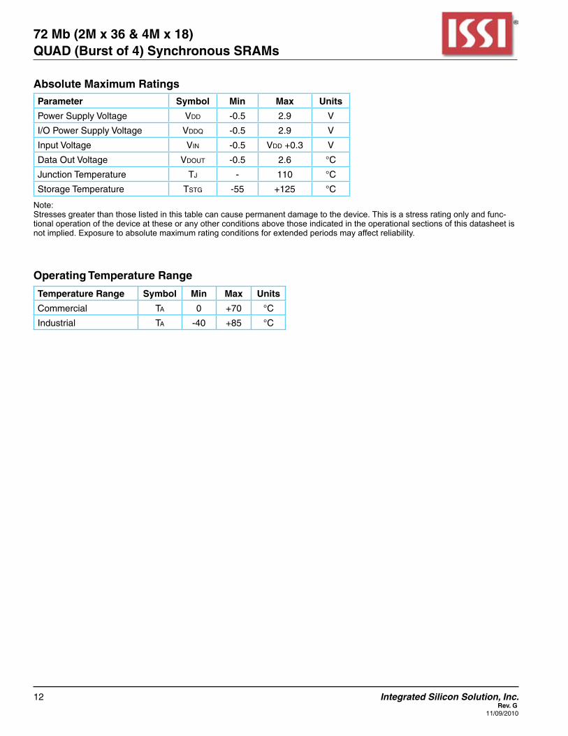
Operating Temperature Range
Temperature Range Symbol Min Max Units
Commercial Ta 0 +70 °C
Industrial Ta -40 +85 °C
Absolute Maximum Ratings
Parameter Symbol Min Max Units
Power Supply Voltage Vdd -0.5 2.9 V
I/O Power Supply Voltage Vddq -0.5 2.9 V
Input Voltage Vin -0.5 Vdd +0.3 V
Data Out Voltage Vdout -0.5 2.6 °C
Junction Temperature Tj - 110 °C
Storage Temperature Tstg -55 +125 °C
Note:Stresses greater than those listed in this table can cause permanent damage to the device. This is a stress rating only and func-tional operation of the device at these or any other conditions above those indicated in the operational sections of this datasheet is not implied. Exposure to absolute maximum rating conditions for extended periods may affect reliability.

Integrated Silicon Solution, Inc. 13Rev. G11/09/2010
72 Mb (2M x 36 & 4M x 18) QUAD (Burst of 4) Synchronous SRAMs
Recommended DC Operating Conditions (Over the Operating Temperature Range)A
Parameter Symbol Minimum Typical Maximum Units Notes
Supply voltage VDD 1.8 - 5% 1.8 + 5% V 1
Output driver supply voltage VDDQ 1.4 1.9 V 1
Input high voltage VIH VREF +0.1 VDDQ + 0.3 V
V
1, 2
1, 3Input low voltage VIL -0.3 VREF - 0.1
Input reference voltage VREF 0.68 0.95 V 1, 5
Clocks signal voltage VIN - CLK -0.3 VDDQ + 0.3 V 1, 4
1. All voltages are referenced to VSS. All VDD, VDDQ, and VSS pins must be connected.2. VIH(Max) AC = See 0vershoot and Undershoot Timings.3. VIL(Min) AC = See 0vershoot and Undershoot Timings.4. VIN-CLK specifies the maximum allowable DC excursions of each clock (K, K, C, and C).5. Peak-to-peak AC component superimposed on VREF may not exceed 5% of VREF.
0vershoot and Undershoot Timings
PBGA Thermal Characteristics
Item Symbol Rating Units
Thermal resistance junction to ambient (airflow = 1m/s) RΘJA 18.6 ° C/W
Thermal resistance junction to case RΘJC 4.3 ° C/W
Thermal resistance junction to pins RΘJB 1.77 ° C/W
VDDQ
20% Min Cycle Time
VDDQ+0.6V
GND-0.6V
GND
20% Min Cycle Time
Overshoot Timing
Undershoot Timing
VIH(Max) AC
VIL(Min) AC
14 Integrated Silicon Solution, Inc. Rev. G
11/09/2010
72 Mb (2M x 36 & 4M x 18) QUAD (Burst of 4) Synchronous SRAMs
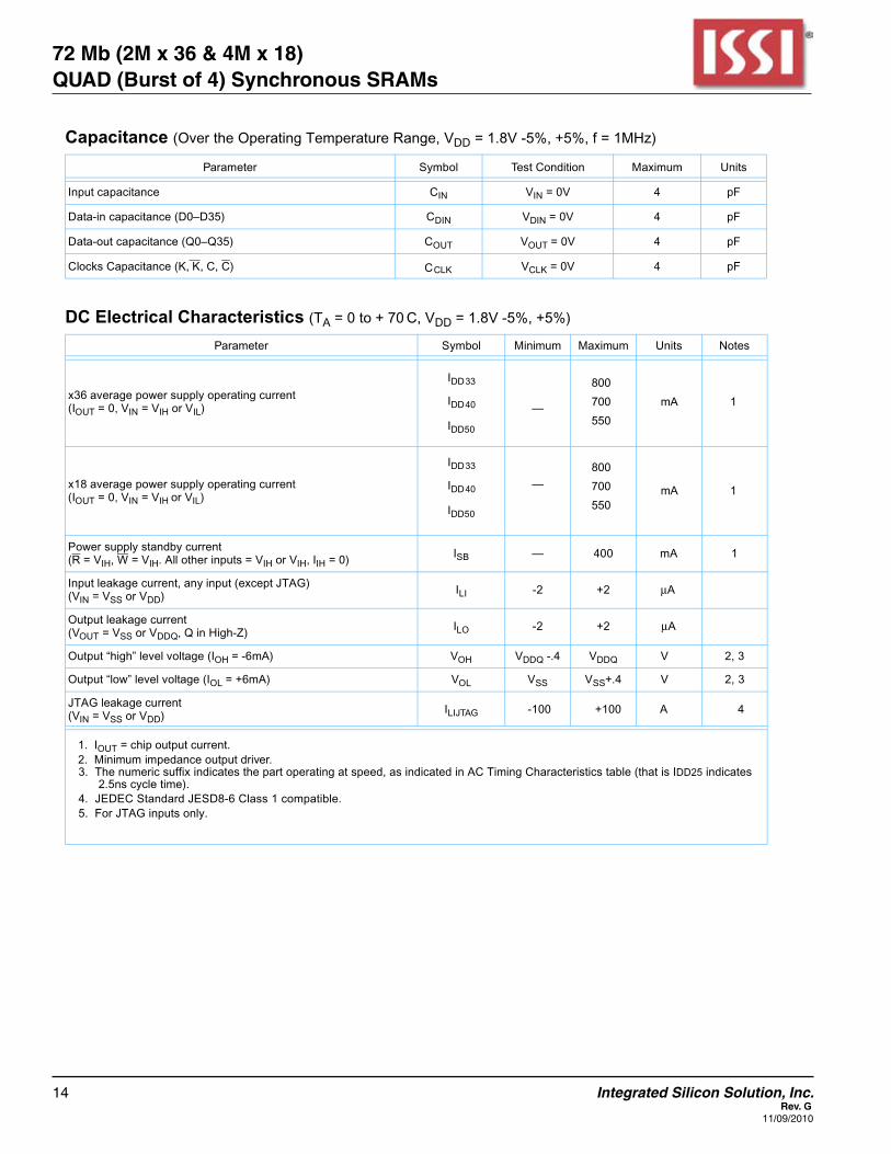
Capacitance (Over the Operating Temperature Range, VDD = 1.8V -5%, +5%, f = 1MHz)
Parameter Symbol Test Condition Maximum Units
Input capacitance CIN VIN = 0V 4 pF
Data-in capacitance (D0–D35) CDIN VDIN = 0V 4 pF
Data-out capacitance (Q0–Q35) C
C
OUT VOUT = 0V 4 pF
Clocks Capacitance (K, K, C, C) CLK VCLK = 0V 4 pF
DC Electrical Characteristics (TA = 0 to + 70 C, VDD = 1.8V -5%, +5%)
Parameter Symbol Minimum Maximum Units Notes
x36 average power supply operating current(IOUT = 0, VIN = VIH or VIL)
IDD50
IDD40
IDD33
IDD50
IDD40
IDD33
—
800
700
550
800
700
550
mA 1
x18 average power supply operating current(IOUT = 0, VIN = VIH or VIL)
— mA 1
Power supply standby current(R = VIH, W = VIH. All other inputs = VIH or VIH, IIH = 0) ISB — 400 mA 1
Input leakage current, any input (except JTAG)(VIN = VSS or VDD) ILI -2 +2 µA
Output leakage current(VOUT = VSS or VDDQ, Q in High-Z) ILO -2 +2 µA
Output “high” level voltage (IOH = -6mA) VOH VDDQ -.4 VDDQ V 2, 3
Output “low” level voltage (IOL = +6mA) VOL VSS VSS+.4 V 2, 3
JTAG leakage current(VIN = VSS or VDD) ILIJTAG -100 +100 A 4
1. IOUT = chip output current.2. Minimum impedance output driver.
3. The numeric suffix indicates the part operating at speed, as indicated in AC Timing Characteristics table (that is IDD25 indicates 2.5ns cycle time). 4. 5. For JTAG inputs only.
JEDEC Standard JESD8-6 Class 1 compatible.
Integrated Silicon Solution, Inc. 15Rev. G11/09/2010
72 Mb (2M x 36 & 4M x 18) QUAD (Burst of 4) Synchronous SRAMs
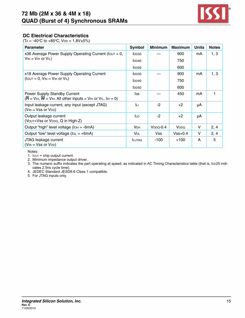
DC Electrical Characteristics(Ta = -40oC to +85oC, Vdd = 1.8V±5%)
Parameter Symbol Minimum Maximum Units Notes
x36 Average Power Supply Operating Current (Iout = 0, Vin = Vih or Vil)
Idd33
Idd40
Idd50
— 900
750
600
mA 1, 3
x18 Average Power Supply Operating Current (Iout = 0, Vin = Vih or Vil)
Idd33
Idd40
Idd50
— 900
750
600
mA 1, 3
Power Supply Standby Current (R = Vih, W = Vih. All other inputs = Vih or Vil, Iih = 0)
Isb — 450 mA 1
Input leakage current, any input (except JTAG) (Vin = Vss or Vdd)
Ili -2 +2 µA
Output leakage current (Vout=Vss or Vddq, Q in High-Z)
Ilo -2 +2 µA
Output “high” level voltage (Ioh = -6mA) Voh Vddq-0.4 Vddq V 2, 4
Output “low” level voltage (Iol = +6mA) Vol Vss Vss+0.4 V 2, 4
JTAG leakage current (Vin = Vss or Vdd)
Ilijtag -100 +100 A 5
Notes:1. Iout = chip output current.2. Minimum impedance output driver.3. Thenumericsuffixindicatesthepartoperatingatspeed,asindicatedinACTimingCharacteristicstable(thatis,Idd25 indi-
cates 2.5ns cycle time).4. JEDECStandardJESD8-6Class1compatible.5. ForJTAGinputsonly.
16 Integrated Silicon Solution, Inc. Rev. G
11/09/2010
72 Mb (2M x 36 & 4M x 18) QUAD (Burst of 4) Synchronous SRAMs
I
3Q
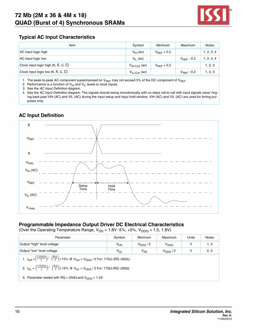
Typical AC Input Characteristics
Item Symbol Minimum Maximum Notes
AC input logic high VIH (ac) VREF + 0.2 1, 2, 3, 4
AC input logic low VIL (ac) VREF - 0.2 1, 2, 3, 4
Clock input logic high (K, K, C, C) VIH-CLK (ac) VREF + 0.2 1, 2, 3
Clock input logic low (K, K, C, C) VIL-CLK (ac) VREF - 0.2 1, 2, 3
1. The peak-to-peak AC component superimposed on VREF may not exceed 5% of the DC component of VREF.2. Performance is a function of VIH and VIL levels to clock inputs.3. See the AC Input Definition diagram.4. See the AC Input Definition diagram. The signals should swing monotonically with no steps rail-to-rail with input signals never ring-
ing back past VIH (AC) and VIL (AC) during the input setup and input hold window. VIH (AC) and VIL (AC) are used for timing pur-poses only.
AC Input Definition
Programmable Impedance Output Driver DC Electrical Characteristics (Over the Operating Temperature Range, VDD = 1.8V -5%, +5%, VDDQ = 1.5, 1.8V)
Parameter Symbol Minimum Maximum Units Notes
Output “high” level voltage VOH VDDQ / 2 VDDQ V 1, 3
Output “low” level voltage VOL VSS VDDQ / 2 V 2, 3
1. IOH = ± 15% @ VOH = VDDQ / 2 For: 175Ω ≤ RQ ≤ 350Ω.
2. IOL = ± 15% @ VOL = VDDQ / 2 For: 175Ω ≤ RQ ≤ 350Ω.
3. Parameter tested with RQ = 250Ω and VDDQ = 1.5V.
VIH (AC)
VREF
VIL (AC)
SetupTime
HoldTime
VREF
K
K
VRAIL
V-RAIL
VDDQ2
------------------ RQ
5--------
⁄
VDDQ2
------------------ RQ
5--------
⁄

Integrated Silicon Solution, Inc. 17Rev. G11/09/2010
72 Mb (2M x 36 & 4M x 18) QUAD (Burst of 4) Synchronous SRAMs
I
3Q
AC Test Conditions (Over the Operating Temperature Range, VDD = 1.8V -5%, +5%, VDDQ = 1.5, 1.8V)
Parameter Symbol Conditions Units Notes
Output driver supply voltage VDDQ 1.5, 1.8 V
Input high level VIH VREF+0.5 V
Input Low Level VIL VREF-0.5 V
Input reference voltage VREF 0.75, 0.9 V
Input rise time TR 0.35 ns
Input fall time TF 0.35 ns
Output timing reference level VREF V
Clocks reference level VREF V
Output load conditions 1, 2
1. See AC Test Loading.2. Parameter tested with RQ = 250Ω and VDDQ = 1.5V.
AC Test Loading
Q50 Ω
50 Ω
5pF
0.75, 0.9V
0.75, 0.9V
Test Comparator

18 Integrated Silicon Solution, Inc. Rev. G
11/09/2010
72 Mb (2M x 36 & 4M x 18) QUAD (Burst of 4) Synchronous SRAMs
AC CHARACTERISTICS(Over the Operating Temperature Range, VDD=1.8V 0.1V)
Notes: 1. All address inputs must meet the specified setup and hold times for all latching clock edges. 2. Control singles are R, W,BW0,BW1 and (BW2, BW3, also for x36) 3. If C,C are tied high, K,K become the references for C,C timing parameters. 4. To avoid bus contention, at a given voltage and temperature tCHQX1 is bigger than tCHQZ. The specs as shown do not imply bus contention because tCHQX1 is a MIN parameter that is worst case at totally different test conditions (0 C, 1.9V) than tCHQZ, which is a MAX parameter (worst case at 70 C, 1.7V) It is not possible for two SRAMs on the same board to be at such different voltage and temperature. 5. Clock phase jitter is the variance from clock rising edge to the next expected clock rising edge. 6. Vdd slew rate must be less than 0.1V DC per 50ns for DLL lock retention. DLL lock time begins once Vdd and input clock are stable. 7. Echo clock is very tightly controlled to data valid/data hold. By design, there is a ns variation from echo clock to data. The data sheet parameters reflect tester guard bands and test setup variations.
PARAMETER SYMBOLMIN MAX MIN MAX MIN MAX
Clock
Clock Cycle Time (K, K, C, C) tKHKH 3.30 7.5 4.00 7.5 5.00 7.5 ns
Clock Phase Jitter (K, K, C, C) tKC var 0.20 0.20 0.20 ns 5
Clock High Time (K, K, C, C) tKHKL 1.32 1.60 2.00 ns
Clock Low Time (K, K, C, C) tKLKH 1.32 1.60 2.00 ns
Clock to Clock (K K , C C ) tKHKH 1.49 1.80 2.20 ns
Clock to data clock (K C , K C ) tKHCH 0.00 0.8 0.00 0.8 0.00 0.8 ns
DLL Lock Time (K, C) tKC lock 1024 1024 1024 cycle 6
Doff Low period to DLL reset 5 5 5 ns
Output Times
C, C High to Output Valid tCHQV 0.45 0.45 0.45 ns 3
C, C High to Output Hold tCHQX -0.45 -0.45 -0.45 ns 3
C, C High to Echo Clock Valid tCHCQV 0.40 0.40 0.40 ns
C, C High to Echo Clock Hold tCHCQX -0.40 -0.40 -0.40 ns
CQ, CQ High to Output Valid tCQHQV 0.27 0.30 0.35 ns 7
CQ, CQ High to Output Hold tCQHQX -0.27 -0.30 -0.35 ns 7
C, High to Output High-Z tCHQZ 0.45 0.45 0.45 ns 3
C, High to Output Low-Z tCHQX1 -0.45 -0.45 -0.45 ns 3
Setup Times
Address valid to K rising edge tAVKH 0.35 0.35 0.4 ns
Control inputs valid to K rising edge tIVKH 0.35 0.35 0.4 ns 2
Data-in valid to K, K rising edge tDVKH 0.35 0.35 0.4 ns
Hold Times
K rising edge to address hold tKHAX 0.35 0.35 0.4 ns
K rising edge to control inputs hold tKHIX 0.35 0.35 0.4 ns
K, K rising edge to data-in hold tKHDX 0.35 0.35 0.4 ns
33 (300 MHz) 40 (250 MHz) 50 (200 MHz)
+ 0.1
UNIT NOTE
tDoLowToReset
Integrated Silicon Solution, Inc. 19Rev. G11/09/2010
72 Mb (2M x 36 & 4M x 18) QUAD (Burst of 4) Synchronous SRAMs
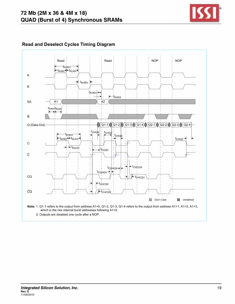
Read and Deselect Cycles Timing Diagram
tCHCQV
tCHCQX
tCHCQX
tCHCQV
tCQHQXtCQHQV
tCHQV
tCHQZ
tCHQX
tCHQVtCHQX
tKLKH
tKHKHtKHKL
tKHIXtIVKH
tKHAX
tAVKH
tKHKH
tKLKH
tKHKHtKHKL
Read Read NOP
A1 A2
Q1-1 Q1-2 Q1-3 Q1-4 Q2-1
NOP
Q2-2 Q2-3 Q2-4
K
K
SA
R
Q (Data-Out)
C
C
CQ
CQ
Don’t Care Undefined
Note: 1. Q1-1 refers to the output from address A1+0, Q1-2, Q1-3, Q1-4 refers to the output from address A1+1, A1+2, A1+3,
2. Outputs are disabled one cycle after a NOP.which is the nex internal burst addresses following A1+0.
tKHCH
20 Integrated Silicon Solution, Inc. Rev. G
11/09/2010
72 Mb (2M x 36 & 4M x 18) QUAD (Burst of 4) Synchronous SRAMs
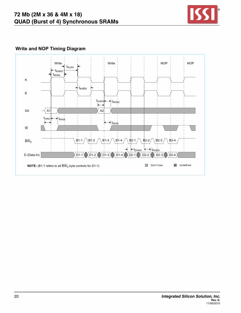
Write and NOP Timing Diagram
tKHDXtDVKH
tKHIX
tKHIXtIVKH
tKHAXtAVKH
tKHKH
tKLKH
ttKHKL
tKHKH
Write Write NOP
A1 A2
D1-1 D1-2 D1-3 D1-4 D2-1 D2-2 D2-3 D2-4
NOP
K
K
SA
W
BWX
D (Data-In)
Don’t Care Undefined
B1-1 B1-2 B1-3 B1-4 B2-1 B2-2 B2-3 B2-4
NOTE: (B1-1 refers to all BWX byte controls for D1-1)

Integrated Silicon Solution, Inc. 21Rev. G11/09/2010
72 Mb (2M x 36 & 4M x 18) QUAD (Burst of 4) Synchronous SRAMs
Read, Write, and NOP Timing Diagram
Read Write Read WriteRead
A1 A2 A3 A4
D2-1 D2-2 D2-3 D4-1 D4-2 D4-3D2-4
Note: If address A3=A2, data Q3-1=D2-1, data Q3-2=D2-2, data Q3-3=D2-3, and
NOP
Q1-1 Q1-2 Q1-3 Q3-1 Q3-2 Q3-3Q1-4
K
K
SA
BWX
R
W
D (Data-In)
D (Data-Out)
C
C
CQ
CQ
Don’t Care Undefined
data Q3-4=D2-4, then write data is forwarded immediately as read results.
NOP
B2-1 B2-2 B2-3 B2-4 B4-1 B4-2 B4-3
22 Integrated Silicon Solution, Inc. Rev. G
11/09/2010
72 Mb (2M x 36 & 4M x 18) QUAD (Burst of 4) Synchronous SRAMs I
3Q
IEEE 1149.1 TAP and Boundary Scan
The SRAM provides a limited set of JTAG functions to test the interconnection between SRAM I/Os and printed circuit board traces or other components. There is no multiplexer in the path from I/O pins to the RAM core.
In conformance with IEEE Standard 1149.1, the SRAM contains a TAP controller, instruction register, boundary scan register, bypass register, and ID register.
The TAP controller has a standard 16-state machine that resets internally on power-up. Therefore, a TRST signal is not required.
Signal List
• TCK: test clock• TMS: test mode select• TDI: test data-in• TDO: test data-out
JTAG DC Operating Characteristics (Over the Operating Temperature Range)AOperates with JEDEC Standard 8-5 (1.8V) logic signal levels
Parameter Symbol Minimum Typical Maximum Units Notes
JTAG input high voltage VIH1 1.3 — VDD+0.3 V 1
JTAG input low voltage VIL1 -0.3 — 0.5 V 1
JTAG output high level VOH1 VDD-0.4 — VDD V 1, 2
JTAG output low level VOL1 VSS — 0.4 V 1, 3
1. All JTAG inputs and outputs are LVTTL-compatible.2. IOH1 = -2mA3. IOL1 = +2mA
JTAG AC Test Conditions (Over the Operating Temperature Range, VDD = 1.8V -5%, +5%)
Parameter Symbol Conditions Units
Input pulse high level VIH1 1.3 V
Input pulse low level VIL1 0.5 V
Input rise time TR1 1.0 ns
Input fall time TF1 1.0 ns
Input and output timing reference level 0.9 V

Integrated Silicon Solution, Inc. 23Rev. G11/09/2010
72 Mb (2M x 36 & 4M x 18) QUAD (Burst of 4) Synchronous SRAMs
I
3Q
JTAG AC Characteristics (Over the Operating Temperature Range, VDD = 1.8V -5%, +5%)
Parameter Symbol Minimum Maximum Units Notes
TCK cycle time tTHTH 20 — ns
TCK high pulse width tTHTL 7 — ns
TCk low pulse width tTLTH 7 — ns
TMS setup tMVTH 4 — ns
TMS hold tTHMX 4 — ns
TDI setup tDVTH 4 — ns
TDI hold tTHDX 4 — ns
TCK low to valid data tTLOV — 7 ns 1
1. See AC Test Loading on page 16.
JTAG Timing Diagram
TCK
TMS
TDI
TDO
tTHTL tTLTH tTHTH
tTHMX
tTHDX
tTLOV
tMVTH
tDVTH

24 Integrated Silicon Solution, Inc. Rev. G
11/09/2010
72 Mb (2M x 36 & 4M x 18) QUAD (Burst of 4) Synchronous SRAMs
I
3Q
Scan Register Definition
Register Name Bit Size x18 or x36
Instruction 3
Bypass 1
ID 32
Boundary Scan 109
ID Register Definition
Part
Field Bit Number and Description
Revision Number(31:29)
Part Configuration (28:12)
JEDEC Code (11:1)
Start Bit (0)
4M x 18 000 000100wx0t0q0b0s0 000 101 001 00 1
2M x 36 000 000100wx0t0q0b0s0 000 101 001 00 1
Part Configuration Definition:wx = 11 for x36, 10 for x18t = 1 for DLL, 0 for non-DLLq = 1 for QUADB4, 0 for DDR-IIb = 1 for burst of 4, 0 for burst of 2s = 1 for separate I/0, 0 for common I/O
Integrated Silicon Solution, Inc. 25Rev. G11/09/2010
72 Mb (2M x 36 & 4M x 18) QUAD (Burst of 4) Synchronous SRAMs
I
3Q
List of IEEE 1149.1 Standard Violations
• 7.2.1.b, e• 7.7.1.a-f• 10.1.1.b, e• 10.7.1.a-d• 6.1.1.d
Instruction Set
Code Instruction TDO Output Notes
000 EXTEST Boundary Scan Register 2,6
001 IDCODE 32-bit Identification Register
010 SAMPLE-Z Boundary Scan Register 1, 2
011 PRIVATE Do not use 5
100 SAMPLE Boundary Scan Register 4
101 PRIVATE Do not use 5
110 PRIVATE Do not use 5
111 BYPASS Bypass Register 3
1. Places Qs in high-Z in order to sample all input data, regardless of other SRAM inputs.2. TDI is sampled as an input to the first ID register to allow for the serial shift of the external TDI data.3. BYPASS register is initiated to VSS when BYPASS instruction is invoked. The BYPASS register also holds the last serially loaded
TDI when exiting the shift-DR state.4. SAMPLE instruction does not place DQs in high-Z.5. This instruction is reserved. Invoking this instruction will cause improper SRAM functionality.6. This EXTEST is not IEEE 1149.1-compliant. By default, it places Q in high-Z. If the internal register on the scan chain is set high,
Q will be updated with information loaded via a previous SAMPLE instruction. The actual transfer occurs during the update IR state after EXTEST is loaded. The value of the internal register can be changed during SAMPLE and EXTEST only.
JTAG Block Diagram
Bypass Register (1 bit)
Identification Register (32 bits)
Instruction Register (3 bits)
TAP Controller
Control Signals
TDI
TMS
TCK
TDO
26 Integrated Silicon Solution, Inc. Rev. G
11/09/2010
72 Mb (2M x 36 & 4M x 18) QUAD (Burst of 4) Synchronous SRAMs
I
3Q
TAP Controller State Machine
Test Logic Reset
Run Test Idle Select DR
Capture DR
Shift DR
Exit1 DR
Pause DR
Exit2 DR
Update DR
Select IR
Capture IR
Shift IR
Exit1 IR
Pause IR
Exit2 IR
Update IR
11
1
00
0
0
1
0
1
1
0
1
1
1
0
01
1
1
0
1
0
0
0
1
1
0
00
0
1
Integrated Silicon Solution, Inc. 27Rev. G11/09/2010
72 Mb (2M x 36 & 4M x 18) QUAD (Burst of 4) Synchronous SRAMs
I
3Q
Boundary Scan Exit Order The same length is used for x18 and x36 I/O configuration.
Order Pin ID Order Pin ID Order Pin ID
1 6R 37 10D 73 2C
2 6P 37 9E 74 3E
3 6N 39 10C 75 2D
4 7P 40 11D 76 2E
5 7N 41 9C 77 1E
6 7R 42 9D 78 2F
7 8R 43 11B 79 3F
8 8P 44 11C 80 1G
9 9R 45 9B 81 1F
10 11P 46 10B 82 3G
11 10P 47 11A 83 2G
12 10N 48 10A 84 1H
13 9P 49 9A 85 1J
14 10M 50 8B 86 2J
15 11N 51 7C 87 3K
16 9M 52 6C 88 3J
17 9N 53 8A 89 2K
18 11L 54 7A 90 1K
19 11M 55 7B 91 2L
20 9L 56 6B 92 3L
21 10L 57 6A 93 1M
22 11K 58 5B 94 1L
23 10K 59 5A 95 3N
24 9J 60 4A 96 3M
25 9K 61 5C 97 1N
26 10J 62 4B 98 2M
27 11J 63 3A 99 3P
28 11H 64 2A 100 2N
29 10G 65 1A 101 2P
30 9G 66 2B 102 1P
31 11F 67 3B 103 3R
32 11G 68 1C 104 4R
33 9F 69 1B 105 4P
34 10F 70 3D 106 5P
35 11E 71 3C 107 5N
36 10E 72 1D 108 5R
109 Internal
Note:1) NC pins as defined on FBGA pinouts on page 2 are read as “don’t cares”.2) State of Internal pin (#109) is loaded via JTAG
28 Integrated Silicon Solution, Inc. Rev. G
11/09/2010
72 Mb (2M x 36 & 4M x 18) QUAD (Burst of 4) Synchronous SRAMs
ORDERING INFORMATION: Commercial Range: 0°C to +70°C Speed Order Part No. Organization Package 300 MHz IS61QDB42M36-300M3 2Mx36 165 BGA
IS61QDB42M36-300M3L 2Mx36 165 BGA, Lead-free IS61QDB44M18-300M3 4Mx18 165 BGA IS61QDB44M18-300M3L 4Mx18 165 BGA, Lead-free
250 MHz IS61QDB42M36-250M3 2Mx36 165 BGA IS61QDB44M18-250M3L 4Mx18 165 BGA, Lead-free
Industrial Range: -40°C to +85°C Speed Order Part No. Organization Package 300 MHz IS61QDB44M18-300M3I 4Mx18 165 BGA
IS61QDB42M36-300M3I 2Mx36 165 BGA IS61QDB42M36-300M3LI 2Mx36 165 BGA, Lead-free
Integrated Silicon Solution, Inc. 29Rev. G11/09/2010
72 Mb (2M x 36 & 4M x 18) QUAD (Burst of 4) Synchronous SRAMs
NO
TE :
1. Controlling dim
ension : mm
Package Outline
12/10/2007