72 IEEE TRANSACTIONS ON CIRCUITS AND SYSTEMS—I: …
14
72 IEEE TRANSACTIONS ON CIRCUITS AND SYSTEMS—I: REGULAR PAPERS, VOL. 51, NO. 1, JANUARY 2004 High-Order Multibit Modulators and Pseudo Data-Weighted-Averaging in Low-Oversampling ADCs for Broad-Band Applications Anas A. Hamoui and Kenneth W. Martin, Fellow, IEEE Abstract—High-speed high-resolution analog-to-digital converters (ADCs) for broad-band communication applications must be designed at a low oversampling ratio (OSR). However, lowering the OSR limits the efficiency of a ADC in achieving a high-resolution A/D conversion. This paper presents several techniques that enable the OSR reduction in ADCs without compromising the resolution. 1) Noise transfer function (NTF). In this paper, a single-stage multibit modulator with a high-order finite-impulse-response NTF is proposed to achieve high signal-to-quantization-noise ratios at low OSRs. Its key fea- tures include: decreased circuit complexity, improved robustness to modulator coefficient variations, and reduced sensitivity to integrator nonlinearities. Its performance is validated through behavioral simulations and compared to traditional mod- ulator structures. 2) Signal transfer function (STF). This paper describes how the STF of a modulator can be designed, independently of the NTF, in order to significantly reduce the harmonic distortion due to opamp nonidealities and to help lower the power dissipation. 3) Dynamic element matching (DEM) is also presented. Data weighted averaging (DWA) has prevailed as the most practical DEM technique to linearize the internal digital-to-analog converter (DAC) of a multibit modulator, especially when the number of DAC elements is large. However, the occurrence of in-band signal-dependent tones, when using DWA at a low OSR, degrades the spurious-free dynamic range. This paper proposes a simple technique, called Pseudo DWA, to solve the DWA tone problem without sacrificing the signal-to-noise ratio. Its implementation adds no extra delay in the feedback loop and requires only minimal additional digital hardware. Existing schemes for DWA tone reduction are also compared. Index Terms— modulators, analog-to-digital converters (ADCs), data-weighted averaging (DWA), digital-to-analog con- version, dynamic element matching (DEM), mismatch shaping. I. INTRODUCTION T HE evolving research toward the development of A/D con- verters (ADCs) with higher speeds and higher resolutions is being equally driven by the demand for high-speed wire- line communication services (as in xDSL modems) as by the need for broadband wireless systems (as in 3G and 4G mobile terminals). Oversampled ADCs are well known for their ability to achieve a high-resolution A/D conversion in low-to- medium speed applications [1]. However, extending these con- Manuscript received January 25, 2003; revised August 26, 2003. This paper was recommended by Guest Editors A. Rodríguez-Vázquez, F. Mediero, and O. Feely. The authors are with the Department of Electrical and Computer Engi- neering, University of Toronto, Toronto, ON M5S 3G4, Canada (e-mail: [email protected]). Digital Object Identifier 10.1109/TCSI.2003.821291 verters to broadband applications requires lowering the over- sampling ratio (OSR) in order for the modulator to be re- alizable within the technology limitations of submicron CMOS processes and to meet a moderate power budget. Consider the single-stage modulator depicted in Fig. 1, with OSR where is the sampling frequency and is the frequency band of the analog input signal. The loss in the signal-to-quantization-noise ratio (SQNR) due to the lowering of the OSR can be compensated for by increasing the noise-shaping order of the loop filter and/or the reso- lution of the -bit quantizer. The impact of increasing the order on the SQNR diminishes significantly as the OSR is reduced. In contrast, the effectiveness of increasing the number of quan- tization bits is independent of the OSR. Other advantages of multibit quantization include enhanced modulator stability as well as relaxed slew-rate and settling requirements on the oper- ational amplifiers (opamps) of the loop-filter integrators. How- ever, the linearity of a multibit modulator is limited by that of its multibit feedback D/A converter (DAC), thereby requiring linearization techniques to correct for the mismatch errors in the DAC elements. Table I summarizes the architecture and performance of published ADCs which are fabricated in a submicron CMOS technology and which are intended for high-speed (signal bandwidth ) and high- resolution (dy- namic range DR and/or spurious-free dynamic range SFDR 12 bits) applications. Observe that all the high-speed high-res- olution ADCs with multibit modulators reported in Table I rely (except [3]) on data weighted averaging (DWA) [25] or a modified version of DWA in order to linearize their internal multibit DACs. DWA is a highly practical and effective dynamic-element-matching (DEM) technique to implement, especially when the number of DAC elements is large. How- ever, at a low OSR, the DWA algorithm must be modified to prevent the occurrence of in-band signal-dependent tones in the output spectrum of the modulator. Although the tone problem of DWA can be circumvented by the modified DWA techniques that have been recently proposed [8], [12], [14], [19], [23], [27], [28], these techniques can significantly degrade the achievable signal-to-noise-plus-distortion ratio (SNDR) or may still generate notable inband tones. This paper presents several techniques that enable the reduc- tion of the OSR in discrete-time modulators without com- promising the resolution: 1057-7122/04$20.00 © 2004 IEEE
Transcript of 72 IEEE TRANSACTIONS ON CIRCUITS AND SYSTEMS—I: …

72 IEEE TRANSACTIONS ON CIRCUITS AND SYSTEMS—I: REGULAR PAPERS, VOL. 51, NO. 1, JANUARY 2004
High-Order Multibit Modulators and PseudoData-Weighted-Averaging in Low-Oversampling
�� ADCs for Broad-Band ApplicationsAnas A. Hamoui and Kenneth W. Martin, Fellow, IEEE
Abstract—High-speed high-resolution �� analog-to-digitalconverters (ADCs) for broad-band communication applicationsmust be designed at a low oversampling ratio (OSR). However,lowering the OSR limits the efficiency of a�� ADC in achievinga high-resolution A/D conversion. This paper presents severaltechniques that enable the OSR reduction in �� ADCs withoutcompromising the resolution. 1) Noise transfer function (NTF).In this paper, a single-stage multibit �� modulator with ahigh-order finite-impulse-response NTF is proposed to achievehigh signal-to-quantization-noise ratios at low OSRs. Its key fea-tures include: decreased circuit complexity, improved robustnessto modulator coefficient variations, and reduced sensitivity tointegrator nonlinearities. Its performance is validated throughbehavioral simulations and compared to traditional �� mod-ulator structures. 2) Signal transfer function (STF). This paperdescribes how the STF of a �� modulator can be designed,independently of the NTF, in order to significantly reduce theharmonic distortion due to opamp nonidealities and to help lowerthe power dissipation. 3) Dynamic element matching (DEM) isalso presented. Data weighted averaging (DWA) has prevailedas the most practical DEM technique to linearize the internaldigital-to-analog converter (DAC) of a multibit �� modulator,especially when the number of DAC elements is large. However,the occurrence of in-band signal-dependent tones, when usingDWA at a low OSR, degrades the spurious-free dynamic range.This paper proposes a simple technique, called Pseudo DWA, tosolve the DWA tone problem without sacrificing the signal-to-noiseratio. Its implementation adds no extra delay in the�� feedbackloop and requires only minimal additional digital hardware.Existing schemes for DWA tone reduction are also compared.
Index Terms—�� modulators, analog-to-digital converters(ADCs), data-weighted averaging (DWA), digital-to-analog con-version, dynamic element matching (DEM), mismatch shaping.
I. INTRODUCTION
THE evolving research toward the development of A/D con-verters (ADCs) with higher speeds and higher resolutions
is being equally driven by the demand for high-speed wire-line communication services (as in xDSL modems) as by theneed for broadband wireless systems (as in 3G and 4G mobileterminals). Oversampled ADCs are well known for theirability to achieve a high-resolution A/D conversion in low-to-medium speed applications [1]. However, extending these con-
Manuscript received January 25, 2003; revised August 26, 2003. This paperwas recommended by Guest Editors A. Rodríguez-Vázquez, F. Mediero, andO. Feely.
The authors are with the Department of Electrical and Computer Engi-neering, University of Toronto, Toronto, ON M5S 3G4, Canada (e-mail:[email protected]).
Digital Object Identifier 10.1109/TCSI.2003.821291
verters to broadband applications requires lowering the over-sampling ratio (OSR) in order for the modulator to be re-alizable within the technology limitations of submicron CMOSprocesses and to meet a moderate power budget.
Consider the single-stage modulator depicted in Fig. 1,with OSR where is the sampling frequencyand is the frequency band of the analog input signal.The loss in the signal-to-quantization-noise ratio (SQNR) due tothe lowering of the OSR can be compensated for by increasingthe noise-shaping order of the loop filter and/or the reso-lution of the -bit quantizer. The impact of increasing the order
on the SQNR diminishes significantly as the OSR is reduced.In contrast, the effectiveness of increasing the number of quan-tization bits is independent of the OSR. Other advantages ofmultibit quantization include enhanced modulator stability aswell as relaxed slew-rate and settling requirements on the oper-ational amplifiers (opamps) of the loop-filter integrators. How-ever, the linearity of a multibit modulator is limited by thatof its multibit feedback D/A converter (DAC), thereby requiringlinearization techniques to correct for the mismatch errors in theDAC elements.
Table I summarizes the architecture and performance ofpublished ADCs which are fabricated in a submicronCMOS technology and which are intended for high-speed(signal bandwidth ) and high- resolution (dy-namic range DR and/or spurious-free dynamic range SFDR12 bits) applications. Observe that all the high-speed high-res-olution ADCs with multibit modulators reported inTable I rely (except [3]) on data weighted averaging (DWA)[25] or a modified version of DWA in order to linearize theirinternal multibit DACs. DWA is a highly practical and effectivedynamic-element-matching (DEM) technique to implement,especially when the number of DAC elements is large. How-ever, at a low OSR, the DWA algorithm must be modified toprevent the occurrence of in-band signal-dependent tones inthe output spectrum of the modulator. Although the toneproblem of DWA can be circumvented by the modified DWAtechniques that have been recently proposed [8], [12], [14],[19], [23], [27], [28], these techniques can significantly degradethe achievable signal-to-noise-plus-distortion ratio (SNDR) ormay still generate notable inband tones.
This paper presents several techniques that enable the reduc-tion of the OSR in discrete-time modulators without com-promising the resolution:
1057-7122/04$20.00 © 2004 IEEE

HAMOUI AND MARTIN: HIGHER ORDER MULTIBIT MODULATORS AND PSEUDO DWA FOR BROAD-BAND APPLICATIONS 73
Fig. 1. Linear model of a single-stage�� modulator with a single DAC feedback. Dynamic element matching (DEM) is used to linearize the multibit feedbackDAC. The feedforward path (dashed line) can be used to acheive an STF= 1 without affecting the NTF.
1) Noise Transfer Function (NTF): By fully utilizing theenhanced stability characteristics of multibit quantiza-tion, stable high-order modulators with aggressiveNTFs can be designed to achieve a high SQNR at a lowOSR. Thus, the noise budget of a switched-capacitor(SC) modulator can be almost entirely allocated tothe analog noise sources (mainly, the samplingnoise) in order to minimize the power dissipation.Accordingly, this paper proposes a multibit mod-ulator architecture to realize finite-impulse-response(FIR) NTFs of arbitrary orders. Its key features include:decreased circuit complexity, improved robustness tomodulator coefficient variations, and reduced sensitivityto integrator nonlinearities.
2) Signal Transfer Function (STF): The focus of mod-ulator design has traditionally been on realizing NTFswhich can achieve a high SQNR without destabilizingthe modulator. This paper describes how the design of theSTF can be utilized, independently of the NTF, in order tosignificantly reduce the harmonic distortion due to opampnonidealities in the loop-filter integrators [31] and to helplower the power dissipation.
3) Dynamic Element Matching (DEM): The occurrenceof in-band signal-dependent tones, when using DWA ata low OSR, degrades the SFDR of the modulatorand can preclude using DWA in low-oversamplingADCs. This paper proposes a simple technique, calledPseudo DWA, to remedy the tone behavior of DWAwithout sacrificing the SNDR. Its implementation addsno extra delay in the feedback loop and requiresonly minimal additional digital-hardware and signal-pro-cessing compared to conventional DWA.
The outline of this paper is as follows. Section II describesthe design of the STF to minimize the sensitivity of modu-lators to integrator nonidealities. Section III briefly reviews FIRNTFs and examines the stability of multibit modulators. InSection IV, a single-stage multibit modulator architecture
is proposed to realize FIR NTFs of arbitrary orders and its per-formance is compared to traditional structures. In Section V, theDWA algorithm is briefly reviewed before analyzing the DWAtone behavior. In Section VI, Pseudo DWA is proposed to elim-inate the tones in conventional DWA, its performance is com-pared to previously reported schemes for DWA tone reduction,and its implementation in a test-chip ADC is described.
II. DESIGN OF THE STF
A. Advantages of a Unity-Gain STF
The noise and signal transfer functions of the modulatormodeled in Fig. 1 are, respectively, defined as
NTF (1)
STF NTF (2)
where is the quantization noise. Theerror signal at the input of the loop filter is
STF NTF (3)
Therefore, a unity-gain STF
STF (4)
reduces the error signal entering the loop filter to
NTF (5)
Consequently, the loop filter will only have to processshaped quantization noise. Since, ideally, no input signal is pro-cessed by the loop-filter integrators, no harmonic distortion isgenerated. Accordingly, the modulator sensitivity to integratornonlinearities, due to the nonlinear dc gain and the dynamiceffects (finite bandwidth and slew rate) of the opamps in theloop-filter integrators, is reduced [30], [31].

74 IEEE TRANSACTIONS ON CIRCUITS AND SYSTEMS—I: REGULAR PAPERS, VOL. 51, NO. 1, JANUARY 2004
TABLE IPUBLISHED �� ADCS WHICH ARE DESIGNED FOR HIGH-SPEED (f � 1 MHz) HIGH-RESOLUTION (DR AND/OR SFDR � 12 bits)
APPLICATIONS AND FABRICATED IN A SUBMICRON CMOS TECHNOLOGY
Supply Voltage: A = analog and D = digital power-supply voltages.CMOS Process: xPyM = CMOS process with x poly layers and y metal layers.�� Modulator Architecture: Unless otherwise specified, the �� modulators have a discrete-time architecture. L(Bb) = L-order B-bit single-stagemodulator. L (B b) � L (B b) � L (B b) = cascaded structure with L -order B -bit,L -order B -Bit, and L -order B -bit modulator stages. SF =single-DAC-feedback and DF = distributed-DAC-feedback architecture.

HAMOUI AND MARTIN: HIGHER ORDER MULTIBIT MODULATORS AND PSEUDO DWA FOR BROAD-BAND APPLICATIONS 75
Fig. 2. SC realization of the summation at the quantizer input in Fig. 1.
The reduced distortion, achieved by designing the modu-lator for an STF , is particularly notable at a low OSR forthe following reasons.
1) The sample-to-sample variations in the modulator’s inputsignal and, hence, in the error signal are substan-tial at a low OSR. It is even more so with an FIR NTF(discussed in Section III) whose large out-of-band gainamplifies the out-of-band noise and causes the unfilteredoutput waveform to deviate by many least-significantbits (LSBs) from the desired output waveform after thedecimation filter [33].
2) The attenuation of the integrator nonidealities by theloop is inadequate in reducing the distortion appearing atthe modulator output at a low OSR. For example, con-sider the first integrator stage at the input of the loop filter.Assume that this integrator stage has a gain . Further-more, assume that the distortion error at its output can bemodeled as a white noise. Such distortion error will ap-pear high-pass filtered by at the output ofthe modulator and, therefore, attenuated by a factorof approximately OSR within the signal band.Thus, for every factor of 2 lowering in OSR, the atten-uation of such distortion error by the loop drops byabout 9 dB.
Furthermore, by designing the modulator for an STFand, hence, requiring the opamps in the integrators of the loopfilter to process only shaped quantization noise, a signif-icant reduction in power dissipation can be achieved for thefollowing reasons.
1) Modulation Input-Signal Range: The availablesignal swing at the outputs of the opamps is nolonger shared between the modulator input signaland the shaped quantization noise. For example, withSTF in Fig. 1, the loop-filter output reducesto NTF and, hence, becomesindependent of the modulator input signal . As aresult, the maximum amplitude 1 of is nolonger limited by the available swing for . Hence,
can be increased with respect to the output satu-ration voltage of the opamp in the last integratorof the loop filter. In fact, the modulator can now tolerate
1kxk = max[jx(n)j]
an . In contrast, modulators whosesignal path goes through are typically designed foran between 0.5 and 0.8 to avoid saturatingthe opamps [1]. Furthermore, an SC modulator is de-signed such that the noise of the sampling switchesin the first integrator stage at the modulator input is thedominant noise source within the modulator[8]. Thus,maximizing allows minimizing the input samplingcapacitor needed to lower the noise below thedesired noise-floor for the modulator. Consequently, thepower dissipation needed to achieve a given dynamicrange is minimized [36]. Such power savings are par-ticularly significant in low-voltage low-oversamplingADCs because the in-band signal-to-noise ratio due tothe noise is inversely proportional to andOSR.
2) Opamp DC Gain: The linearity requirements on theopamps are relaxed. Hence, by tolerating some gainand phase errors (due to the finite opamp gains) in thetransfer function of the integrators, opamps with onlymoderate gains can be utilized to realize the integrators.While opamps with moderate dc gains (150 to 300 V/V)are readily obtainable using classical folded-cascode orcurrent-mirror designs, high-gain opamps require eithermultiple gain stages or output-impedance enhancement[35] because of the shrinking supply voltages and thepoor intrinsic gains of the MOS transistors in scaledCMOS technologies. Such gain-boosting techniques forthe opamps significantly increase the power dissipationand degrade the speed.
3) Opamp Slew Rate: The signal-path delay is reduced tozero. Decreasing the number of delays in the signal pathdecreases the sample-to-sample variations in the errorsignal at the loop-filter input. As a result, for a tar-geted settling performance in the SC integrators of theloop filter (especially in the first integrator stage whichhas the largest impact on the overall modulator perfor-mance), the required slew rate and, hence, power dissi-pation in the opamps are relaxed [12]. In a single-stage
modulator, the number of delays in the signal path istypically equal to the noise-shaping order of the loopfilter. However, by designing the modulator for anSTF , the signal-path delay can be reduced to zero. Ac-

76 IEEE TRANSACTIONS ON CIRCUITS AND SYSTEMS—I: REGULAR PAPERS, VOL. 51, NO. 1, JANUARY 2004
(a)
(b)
(c)
Fig. 3. (a) Fourth-order �� modulator with a distributed DAC feedback. The dashed feedforward paths are used to achieve an STF = 1, without affecting theNTF. (b), (c) The feedback paths of the modulator in (a) are replaced with feedforward paths, without affecting the NTF. The dashed feedforward paths are thenused to achieve an STF = 1, resulting in modulator topologies that are equivalent to (a) but with reduced input loading.
cordingly, high-order single-stage modulators can berealized without increasing the requirements of the slewrate and, hence, power dissipation in the opamps of theSC integrators.
In summary, designing a modulator with an STFis generally more desirable than any other STF characteristicbecause it significantly reduces the sensitivity of the modu-lator to integrator nonidealities (as the analog input signal doesnot flow through the loop filter) and, hence, helps minimizingthe power dissipation.
B. Unity-Gain STF in a Single-Feedback Modulator
In a modulator with a single DAC feedback (i.e., asingle-loop modulator), an STF can be achievedwithout affecting the NTF by adding the modulator’s inputsignal to the quantizer’s input signal [31], [32], as shown bythe feedforward path (the dashed line) in Fig. 1.
In an SC realization of the modulator in Fig. 1, the sum-mation at the quantizer input can be implemented using an SCnetwork [31], as shown in Fig. 2 where a two-phase nonoverlap-ping clock is assumed. However, such passive implementation
entails a factor of two drop in the quantizer’s input signal .Therefore, in order to maintain the desired performance for the
modulator, the quantizer’s reference voltage must bescaled down by a factor of two from its nominal value. How-ever, this also scales down (by the same factor) the quantizer’sstep size and, hence, the maximum acceptable accuracy for thecomparators in the quantizer. Accordingly, comparators with ahigher resolution will be required.
C. Unity-Gain STF in a Distributed-Feedback Modulator
In a modulator with a distributed DAC feedback (i.e.,a multiloop modulator) [9], [37], an STF can beachieved without affecting the NTF by adding the modulator’sinput signal to the outputs of the loop-filter integrators,as shown by the weighted feedforward paths (dashed lines)in Fig. 3(a). This cancels the spectral components of atthese nodes and, consequently, the loop-filter integrators willonly have to process shaped quantization-noise. However, thistechnique significantly increases the loading at the modulatorinput. An alternative approach ((Fig. 3(b)) is to first replacethe distributed feedback paths, except for the first and last
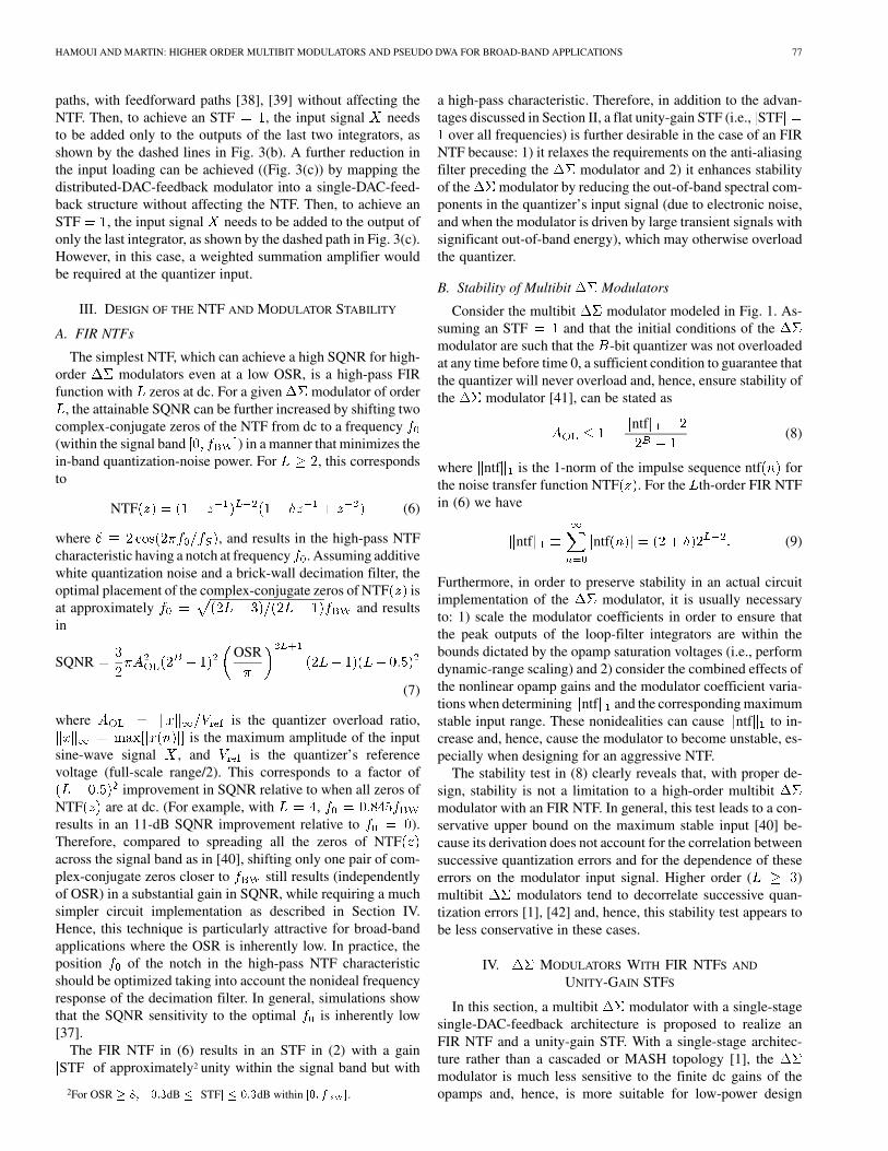
HAMOUI AND MARTIN: HIGHER ORDER MULTIBIT MODULATORS AND PSEUDO DWA FOR BROAD-BAND APPLICATIONS 77
paths, with feedforward paths [38], [39] without affecting theNTF. Then, to achieve an STF , the input signal needsto be added only to the outputs of the last two integrators, asshown by the dashed lines in Fig. 3(b). A further reduction inthe input loading can be achieved ((Fig. 3(c)) by mapping thedistributed-DAC-feedback modulator into a single-DAC-feed-back structure without affecting the NTF. Then, to achieve anSTF , the input signal needs to be added to the output ofonly the last integrator, as shown by the dashed path in Fig. 3(c).However, in this case, a weighted summation amplifier wouldbe required at the quantizer input.
III. DESIGN OF THE NTF AND MODULATOR STABILITY
A. FIR NTFs
The simplest NTF, which can achieve a high SQNR for high-order modulators even at a low OSR, is a high-pass FIRfunction with zeros at dc. For a given modulator of order
, the attainable SQNR can be further increased by shifting twocomplex-conjugate zeros of the NTF from dc to a frequency(within the signal band ) in a manner that minimizes thein-band quantization-noise power. For , this correspondsto
NTF (6)
where , and results in the high-pass NTFcharacteristic having a notch at frequency . Assuming additivewhite quantization noise and a brick-wall decimation filter, theoptimal placement of the complex-conjugate zeros of NTF isat approximately and resultsin
SQNROSR
(7)
where is the quantizer overload ratio,is the maximum amplitude of the input
sine-wave signal , and is the quantizer’s referencevoltage (full-scale range/2). This corresponds to a factor of
improvement in SQNR relative to when all zeros ofNTF are at dc. (For example, with ,results in an 11-dB SQNR improvement relative to ).Therefore, compared to spreading all the zeros of NTFacross the signal band as in [40], shifting only one pair of com-plex-conjugate zeros closer to still results (independentlyof OSR) in a substantial gain in SQNR, while requiring a muchsimpler circuit implementation as described in Section IV.Hence, this technique is particularly attractive for broad-bandapplications where the OSR is inherently low. In practice, theposition of the notch in the high-pass NTF characteristicshould be optimized taking into account the nonideal frequencyresponse of the decimation filter. In general, simulations showthat the SQNR sensitivity to the optimal is inherently low[37].
The FIR NTF in (6) results in an STF in (2) with a gainSTF of approximately2 unity within the signal band but with
2For OSR � 8;�0:3dB � jSTFj � 0:3dB within [0; f ].
a high-pass characteristic. Therefore, in addition to the advan-tages discussed in Section II, a flat unity-gain STF (i.e., STF
over all frequencies) is further desirable in the case of an FIRNTF because: 1) it relaxes the requirements on the anti-aliasingfilter preceding the modulator and 2) it enhances stabilityof the modulator by reducing the out-of-band spectral com-ponents in the quantizer’s input signal (due to electronic noise,and when the modulator is driven by large transient signals withsignificant out-of-band energy), which may otherwise overloadthe quantizer.
B. Stability of Multibit Modulators
Consider the multibit modulator modeled in Fig. 1. As-suming an STF and that the initial conditions of themodulator are such that the -bit quantizer was not overloadedat any time before time 0, a sufficient condition to guarantee thatthe quantizer will never overload and, hence, ensure stability ofthe modulator [41], can be stated as
ntf(8)
where ntf is the 1-norm of the impulse sequence ntf forthe noise transfer function NTF . For the th-order FIR NTFin (6) we have
ntf ntf (9)
Furthermore, in order to preserve stability in an actual circuitimplementation of the modulator, it is usually necessaryto: 1) scale the modulator coefficients in order to ensure thatthe peak outputs of the loop-filter integrators are within thebounds dictated by the opamp saturation voltages (i.e., performdynamic-range scaling) and 2) consider the combined effects ofthe nonlinear opamp gains and the modulator coefficient varia-tions when determining ntf and the corresponding maximumstable input range. These nonidealities can cause ntf to in-crease and, hence, cause the modulator to become unstable, es-pecially when designing for an aggressive NTF.
The stability test in (8) clearly reveals that, with proper de-sign, stability is not a limitation to a high-order multibitmodulator with an FIR NTF. In general, this test leads to a con-servative upper bound on the maximum stable input [40] be-cause its derivation does not account for the correlation betweensuccessive quantization errors and for the dependence of theseerrors on the modulator input signal. Higher order ( )multibit modulators tend to decorrelate successive quan-tization errors [1], [42] and, hence, this stability test appears tobe less conservative in these cases.
IV. MODULATORS WITH FIR NTFS AND
UNITY-GAIN STFS
In this section, a multibit modulator with a single-stagesingle-DAC-feedback architecture is proposed to realize anFIR NTF and a unity-gain STF. With a single-stage architec-ture rather than a cascaded or MASH topology [1], themodulator is much less sensitive to the finite dc gains of theopamps and, hence, is more suitable for low-power design

78 IEEE TRANSACTIONS ON CIRCUITS AND SYSTEMS—I: REGULAR PAPERS, VOL. 51, NO. 1, JANUARY 2004
Fig. 4. Proposed �� modulator of order L (L � 3). The feedforward coefficients a (i = 3; . . . ; L) needed to realize the FIR NTF in (6) are given in Table II.Here, � 1=(1 � z ).
TABLE IIFEEDFORWARD COEFFICIENTS a (i = 3; . . . ; L) NEEDED TO REALIZE
THE LTH-ORDER (L � 3) FIR NTF IN (6) USING THE PROPOSED
�� MODULATOR IN FIG. 4
For L = 4, path a consists of two parallel paths: a non-delaying path withcoefficient 2 and a delaying path with coefficient 2z .
in scaled CMOS technologies. Furthermore, a single DACfeedback rather than a distributed DAC feedback within themultibit modulator significantly reduces the complexityof implementing the analog and DAC-linearization circuits,the chip area, and the power dissipation, especially whenbootstrapped switches are needed in low-voltage designs [24].
A. Proposed Modulator
To implement an FIR NTF (with ) and a unity-gainSTF, the multibit modulator architecture shown in Fig. 4 isproposed [43]. This mathematical model can be directly mappedto an SC circuit [35]. The modulator coefficients needed to re-alize the FIR NTF in (6) are given in Table II. Except for thefinite-zero loop-gain parameter , these coefficients are inde-pendent of e OSR and . The implementation of the com-plex-conjugate zeros in the FIR NTF is achieved by one ad-ditional local feedback around the last two integrators in theloop filter (thereby forming a resonator) and, hence, requiresvery little analog circuitry. Although integrators with both de-laying and nondelaying paths are required to implement an FIRNTF, the high-frequency settling properties of the proposed ar-chitecture is enhanced by designing the modulator with nodelay-free loops and by interconnecting the loop-filter integra-tors such that the worst-case settling when correspondsto two opamps settling in series.
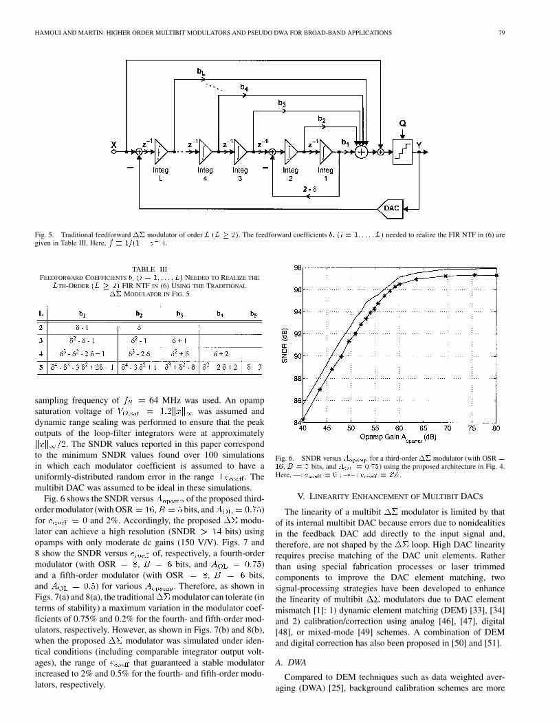
B. Traditional Feedforward Modulator
Alternatively, an FIR NTF can also be implemented using thetraditional feedforward modulator structure [10], [14], [44]
as shown in Fig. 5. The corresponding modulator coefficientsneeded to realize the FIR NTF in (6) are given in Table III. Notethat the modulator proposed in [31] falls as a special caseof the feedforward modulator in Fig. 5 when and
.The proposed modulator in Fig. 4 offers the following
advantages over the traditional modulator in Fig. 5.
1) The circuit complexity is reduced by not requiring aweighted summation amplifier before the quantizer. Inthe proposed modulator (Fig. 4), the summation ofthe signals in the feedforward paths is performed withinthe last integrator stage of the loop filter.
2) The sensitivity of the modulator to process variationsin the modulator coefficients is significantly reduced, asdemonstrated by the simulation results in Section IV-C.This improved robustness to coefficient variations couldbe attributed to the reduced number of feedforward pathsin the proposed modulator, as every feedforward pathcorresponds to a cancellation in the NTF and STF of themodulator.
3) After proper dynamic range scaling, the modulator coeffi-cients needed to realize an FIR NTF using the traditionalfeedforward structure (Fig. 5) have larger ratios comparedto those in the proposed architecture (Fig. 4), thereby in-troducing large capacitor-ratio spreads in SC implemen-tations. For example, in a fifth-order modulator with anOSR and an optimal zero placement, the largest co-efficient ratio is 5 in the proposed architecture (Table II)while the coefficient ratio is 390.5 in the traditionaltopology (Table III).
C. Behavioral Simulation Results
The modulators in Figs. 4 and 5 were simulated inSIMULINK. The gain and phase errors in the transfer functionof the loop-filter integrators, due to the nonlinear dc gains ofthe opamps, were modeled as described in [45]. The opampswere assumed to have nonlinear dc gains corresponding to aninput–output transfer curve in the form of a hyperbolic tangentwith a maximum dc gain of and an output saturationvoltage of . A sine-wave signal with an amplitudeand a frequency OSR was applied at the input. A
HAMOUI AND MARTIN: HIGHER ORDER MULTIBIT MODULATORS AND PSEUDO DWA FOR BROAD-BAND APPLICATIONS 79
Fig. 5. Traditional feedforward �� modulator of order L (L � 2). The feedforward coefficients b (i = 1; . . . ; L) needed to realize the FIR NTF in (6) aregiven in Table III. Here, � 1=(1� z ).
TABLE IIIFEEDFORWARD COEFFICIENTS b (i = 1; . . . ; L) NEEDED TO REALIZE THE
LTH-ORDER (L � 2) FIR NTF IN (6) USING THE TRADITIONAL
�� MODULATOR IN FIG. 5
sampling frequency of 64 MHz was used. An opampsaturation voltage of was assumed anddynamic range scaling was performed to ensure that the peakoutputs of the loop-filter integrators were at approximately
. The SNDR values reported in this paper correspondto the minimum SNDR values found over 100 simulationsin which each modulator coefficient is assumed to have auniformly-distributed random error in the range . Themultibit DAC was assumed to be ideal in these simulations.
Fig. 6 shows the SNDR versus of the proposed third-order modulator (with OSR , bits, and )for and 2%. Accordingly, the proposed modu-lator can achieve a high resolution (SNDR bits) usingopamps with only moderate dc gains (150 V/V). Figs. 7 and8 show the SNDR versus of, respectively, a fourth-ordermodulator (with OSR , bits, and )and a fifth-order modulator (with OSR , bits,and ) for various . Therefore, as shown inFigs. 7(a) and 8(a), the traditional modulator can tolerate (interms of stability) a maximum variation in the modulator coef-ficients of 0.75% and 0.2% for the fourth- and fifth-order mod-ulators, respectively. However, as shown in Figs. 7(b) and 8(b),when the proposed modulator was simulated under iden-tical conditions (including comparable integrator output volt-ages), the range of that guaranteed a stable modulatorincreased to 2% and 0.5% for the fourth- and fifth-order modu-lators, respectively.
Fig. 6. SNDR versus A for a third-order �� modulator (with OSR =16, B = 5 bits, and A = 0:75) using the proposed architecture in Fig. 4.Here, —: e = 0 ; –�– : e = 2%.
V. LINEARITY ENHANCEMENT OF MULTIBIT DACS
The linearity of a multibit modulator is limited by thatof its internal multibit DAC because errors due to nonidealitiesin the feedback DAC add directly to the input signal and,therefore, are not shaped by the loop. High DAC linearityrequires precise matching of the DAC unit elements. Ratherthan using special fabrication processes or laser trimmedcomponents to improve the DAC element matching, twosignal-processing strategies have been developed to enhancethe linearity of multibit modulators due to DAC elementmismatch [1]: 1) dynamic element matching (DEM) [33], [34]and 2) calibration/correction using analog [46], [47], digital[48], or mixed-mode [49] schemes. A combination of DEMand digital correction has also been proposed in [50] and [51].
A. DWA
Compared to DEM techniques such as data weighted aver-aging (DWA) [25], background calibration schemes are more

80 IEEE TRANSACTIONS ON CIRCUITS AND SYSTEMS—I: REGULAR PAPERS, VOL. 51, NO. 1, JANUARY 2004
(a)
(b)
Fig. 7. SNDR versus e for a fourth-order��modulator (with OSR = 8,B = 6 bits, and A = 0:75) using: (a) the traditional topology in Fig. 5 and(b) the proposed architecture in Fig. 4. Here, –�–: ideal opamp; –�–:A =
60 dB; –+–: A = 50 dB.
expensive to implement in terms of system design complexity,hardware requirement, and power consumption. Indeed, allhigh-speed high-resolution ADCs with multibitmodulators reported in Table I rely (except [3]) on DWA or amodified version of DWA in order to linearize their internalmultibit DACs. In such high-speed modulators, the com-plexity of the DEM algorithm becomes a concern becausethe delay introduced by the DEM selection logic in thefeedback loop (Fig. 1) can limit the maximum achievable clockspeed for the modulator. In that respect, DWA is a highlypractical DEM technique to implement, especially when thenumber of DAC elements is large.
In DWA, the DAC unit elements participating in the D/Aconversion are selected sequentially from the DAC array,beginning with the next available unused element. A pointer,hereafter called the index pointer , directs the element-se-lection process. Through such rotational element-selectionprocess, DWA achieves first-order high-pass shaping of theDAC mismatch errors [33], [52]. However, it can also introduce
(a)
(b)
Fig. 8. SNDR versus e for a fifth-order �� modulator (with OSR = 8,B = 6 bits, and A = 0:5) using: (a) the traditional topology in Fig. 5 and(b) the proposed architecture in Fig. 4. Here, –�–: ideal opamp; –�–:A =
60 dB; –+–: A = 50 dB.
in-band signal-dependent tones in the modulator’s outputspectrum ((as depicted in Fig. 9(a)) [25], [53].
B. Tone Behavior of DWA
In DWA, because the same set of DAC elements is used cycli-cally and repeatedly under the guide of a single pointer [53], theelement mismatch errors translate to tones at the DAC outputwhen the DAC input codes have a periodic pattern. These tonesadd directly to the modulator’s input signal and appear unshapedat the modulator output. Out-of-band tones generated by DWAmay then fold back to the signal band due to modulation by themodulator’s output waveform. The tone behavior of DWA de-pends on the number of DAC elements, the pattern of the DACelement mismatch, the amplitude and frequency of the modu-lator’s input signal, and various circuit parameters which affectthe modulator’s output waveform [26], [53]. For example, con-sider the case when the consecutive input codes to the -ele-ment DAC in Fig. 1 have the same value (i.e.,

HAMOUI AND MARTIN: HIGHER ORDER MULTIBIT MODULATORS AND PSEUDO DWA FOR BROAD-BAND APPLICATIONS 81
(a) (b)
(c) (d)
Fig. 9. Output spectrum of the �� modulator using: (a) DWA [25],(b) P-DWA [12], (c) Pseudo DWA with n = 128, and (d) Pseudo DWAwith n = 64. (Input signal: �30 dBFS at f =2048.)
). As is common, define the mismatch error in the DACunit element as
where (10)
The DWA algorithm will select DAC unit elements in a ro-tational manner, making a complete rotation (with the indexpointer returning to its exact starting point) every clockcycles, where is the greatest common divisor of and .As a result, the DAC mismatch noise will be a periodic sequence
(11)of period (where ), and its power spectrumwill take the form of tones at frequencies [26]
(12)
Thus, in general, for an -element DAC, the lowest tone fre-quency can be at with DWA. If the maximum possibleinput frequency to the modulator is OSR ,then the constraint that the th harmonic of the modulator’sinput signal does not fall back into the signal bandwidth afterbeing modulated by the DWA tone at requires that [53]
OSR (13)
In summary, the tone problem of DWA degrades the SFDRof the modulator and can preclude using DWA at a lowOSR, especially when the number of DAC elements (quantiza-
tion bits) is large. In the following, a simple technique will beproposed to solve this problem.
VI. PSEUDO DWA
A. Pseudo DWA Algorithm
Consider an -element DAC with input code . In con-ventional DWA, the DAC unit elements selected at time arethose from to mod , by increasingorder. The index pointer (i.e., the address of the nextavailable unused element) is stored in a digital register. Everyclock cycle, the index pointer is incremented modulus bythe DAC input code
(14)
The technique proposed in this paper, called Pseudo DWA,modifies the DWA scheme by periodically inverting the LSB ofthe DAC input code used to update the index pointer in(14)[29]. Let denote the number of clock cycles betweeneach such LSB inversion. Then, the element-selection processin Pseudo DWA is essentially similar to conventional DWA ex-cept that, every clock cycles, a DAC element is either rese-lected or skipped depending on whether the previous DAC inputcode was, respectively, odd or even. For example, assume that
has a value in (14). If the corresponding iseven, its LSB inversion will increase by 1. As a result,on the next clock cycle (i.e., at time ), the Pseudo DWAalgorithm will select DAC elements starting with element(i.e., element is skipped). Alternatively, if the corresponding
is odd, its LSB inversion will decrement by 1.As a result, on the next clock cycle, the Pseudo DWA algorithmwill select DAC elements starting with element (i.e., el-ement is reselected). This simple modification to DWAbreaks the cyclic nature of the element-selection process and,hence, reduces the tone behavior.
B. Performance of Pseudo DWA
The Pseudo DWA algorithm is implemented in a third-orderADC with a 5-bit quantizer, a 31-element DAC, and
a OSR. The ADC is based on the proposedmodulator (Fig. 4), with the NTF having one zero at dc andtwo complex-conjugate zeros at the signal-band edge .The results reported in this paper correspond to the average of100 SIMULINK simulations assuming a random DAC elementmismatch of 0.5% . These behavioral simulations accountfor the nonlinear dc gains of the opamps in the loop-filter inte-grators as described in Section IV-C, with V/V.Furthermore, these simulations include the quantization noiseand the DAC mismatch noise, but no other analog devicenoise. Since simulations with an ideal DAC showed no obviousin-band tones in the output spectrum of the modulator, itcan be assumed that, with a nonideal DAC, any in-band tonesare generated by the DAC element-mismatch errors.
In Pseudo DWA, the choice of is a compromise betweenlinearity and resolution. If is too large corre-sponds to conventional DWA), the signal-dependent tones will

82 IEEE TRANSACTIONS ON CIRCUITS AND SYSTEMS—I: REGULAR PAPERS, VOL. 51, NO. 1, JANUARY 2004
TABLE IVACHIEVABLE PEAK SNDR USING VARIOUS DWA SCHEMES IN A
THIRD-ORDER �� MODULATOR WITH OSR = 16, B = 5 BITS,AND M = 31 ELEMENTS. A RANDOM DAC-ELEMENT
MISMATCH OF 0.5% IS ASSUMED. (INPUT SIGNAL:�2 dBFS AT f =2048)
not be eliminated. If is too small, different DAC elementswill be used at significantly different rates. Simulations showthat this increases the inband mismatch noise and degrades theSNDR. Deriving an analytical expression for the optimum valueof is rather complex because the DWA tone behavior de-pends on the various circuit parameters which affect the mod-ulator output waveform (as discussed in Section V). However,for a given modulator, simple behavioral simulations canbe easily used to find the appropriate value of . For the
modulator described above, the simulation results presentedbelow indicate that an between 64 and 128 is a good choicefor preventing the DWA tones without sacrificing the SNDR.These results have also been verified experimentally in [24].
Fig. 9(a) shows strong in-band tones in the output spectrumof the modulator when using DWA. When using PseudoDWA and (Fig. 9(c)) or (Fig. 9(d)), thesetones are smoothed in all frequencies and no notable tones arepresent in the signal band. This is accompanied with some in-crease in the inband noise. However, as depicted in Fig. 10, thedegradation in SNDR compared to DWA is within 1 dB (for
) over the full range of input signal levels. This im-plies that, if the DAC mismatch noise floor is below the overallnoise floor of the ADC, it is beneficial to use Pseudo DWA andimprove the SFDR.
C. Comparison of Pseudo DWA To Other DWA Schemes
A number of techniques have been proposed to solve the toneproblem in DWA. These techniques can be classified into fourcategories: 1) Dithering [25]; 2) Incremental DWA (IDWA)[14], [26]; 3) DWA with multiple data-directed index pointers,as in Bi-Directional DWA (Bi-DWA) [8] and Partitioned DWA(P-DWA) [12]; 4) DWA with randomized index pointer, asin Rotated DWA (RDWA) [19], [27], Randomized DWA(RnDWA) [23], [28], and Pseudo DWA [24], [29]. A summarydescription of these techniques is presented in [29].
Fig. 10. SNDR versus input signal levels when using: — DWA [25];–�– Pseudo DWA; –�– P-DWA [12]; –+– RnDWA [28] with an idealimplementation.
Fig. 11. Maximum in-band tone versus input signal levels when using: —DWA [25]; –�– Pseudo DWA; –�– P-DWA [12]; –+– RnDWA [28] with anideal implementation.
Table IV compares the peak SNDR when using the abovetechniques for DWA tone reduction. In classical DWA, the effi-ciency of the DAC mismatch errors averaging to zero is deter-mined by the rate of using each DAC unit element [25]. The useof an extra DAC element in IDWA, the switching between sep-arate pointers in Bi-DWA, and the frequent jumps in the indexpointer in RnDWA, reduce this rate and degrade the SNDR. ForP-DWA, Fig. 10 shows that the degradation in SNDR comparedto DWA is within 1.2 dB for input signal levels above dB,but is over 3 dB for lower levels. Furthermore, as shown inFig. 9(b), P-DWA still generates notable signal-dependent toneswithin the signal band.
Fig. 11 shows the maximum in-band tone relative to the av-erage tone power. Compared to DWA, reductions of about 15,

HAMOUI AND MARTIN: HIGHER ORDER MULTIBIT MODULATORS AND PSEUDO DWA FOR BROAD-BAND APPLICATIONS 83
Fig. 12. Implementation of the Pseudo DWA algorithm.
16, and 18 dB in the maximum in-band tone are achieved usingPseudo DWA, P-DWA, and RnDWA (with an ideal implemen-tation [29]), respectively. Note that, in general, a modified DWAtechnique cannot completely eliminate the in-band DWA tonesand achieve a smooth DAC noise floor over all input signallevels, unless a perfectly random component is introduced inthe DAC element-selection process (for example, in an idealimplementation of a randomized DWA technique [29]). How-ever, assuming a 0.5% DAC-element mismatch in the ADCdescribed above, behavioral simulations show that the largestin-band tone with Pseudo DWA is well below the level of the
noise floor for the ADC. Thus, such in-band tone willnot be visible in the ADC output spectrum and will not degradeits performance.
D. Implementation of Pseudo DWA
The implementation of any DEM algorithm is critical for theachievable clock speed because the DEM block (element-selec-tion logic in Fig. 1) adds extra delay in the feedback loop.In an SC implementation of a modulator, the -bit quan-tizer is typically realized using as an -level flash ADC and atwo-phase nonoverlapping clock is used. Only half a clock pe-riod is available for the thermometer output code of the flashADC to be generated, processed by the DEM block, and D/Aconverted by the DAC. Therefore, the DEM logic must be opti-mized for minimal delay in the feedback path [9].
Fig. 12 shows the implementation of the Pseudo DWA algo-rithm (with ) in a ADC with a 5-bit quantizerand a 31-element DAC [24]. Here, the 5-bit quantizer is real-ized using a flash ADC with a 31-digit thermometer output-code
. A five-stage logarithmic shifter in the feedback pathprovides the rotation of the 31-digit code as requiredby the Pseudo DWA algorithm, thereby generating an equiva-lent 31-digit code which selects the DAC unit-elements(Fig. 1). The 5-bit control signal of the shifter corresponds to theindex pointer and should be stable during phase whenthe thermometer code ripples through the shifter. The shifter isimplemented using only NMOS transistors, with level restorersafter the third and fifth stages to achieve minimal delay. The
index pointer is updated every clock cycle as follows:1) an encoder converts the 31-digit thermometer output-code
to a 5-bit binary output-code ; 2) a 5-bit adder, withend-around carry, increments the index pointer mod-ulus 31 by the output code and generates the next indexpointer (i.e., the index pointer to be used at thenext ); 3) every 64 clock cycles , the LSB ofthe quantizer output code is inverted before updating theindex-pointer register. A 6-bit Johnson counter and a 2:1 muxare used to control the timing of the LSB inversion. This is theonly additional hardware required to implement Pseudo DWAinstead of DWA. Accordingly, Pseudo DWA adds no extra delayin the critical feedback path (phase ) of the loop.
VII. CONCLUSION
Techniques to modify single-feedback and distributed-feed-back modulator topologies in order to achieve a unity-gainSTF without affecting the NTF were described. Such an STFis generally more desirable than any other STF characteristicas it reduces the modulator sensitivity to integrator nonideali-ties and, hence, helps minimizing the power dissipation. Next, amultibit modulator was proposed to realize high-order FIRNTFs (with a pair of complex-conjugate zeros optimally placedacross the signal band) to achieve high SQNRs at low OSRs.Its circuit implementation is simpler than traditional mod-ulator structures and simulations confirm its reduced sensitivityto integrator nonlinearities and its improved robustness to co-efficient variations. Thus, the proposed modulator is par-ticularly suitable for realizing broadband low-distortion ADCs.Finally, Pseudo DWA was proposed to remedy the tone behaviorof DWA without sacrificing the SNDR. It implementation addsno extra delay in the feedback loop and requires only min-imal additional digital-signal-processing. Simulations confirmthe improved accuracy achievable by Pseudo DWA at low OSRs.
ACKNOWLEDGMENT
The authors would like to thank Prof. G. Temes andMr. J. Silva of Oregon State University, and Dr. J. Steensgaardof Esion for their fruitful comments.

84 IEEE TRANSACTIONS ON CIRCUITS AND SYSTEMS—I: REGULAR PAPERS, VOL. 51, NO. 1, JANUARY 2004
REFERENCES
[1] S. R. Norsworthy, R. Schreier, and G. C. Temes, Eds., Delta-Sigma DataConverters Theory, Design, and Simulation. New York: IEEE Press,1996.
[2] B. P. Brandt and B. A. Wooley, “A 50-MHz multibit sigma-delta mod-ulator for 12-bit 2-MHz A/D conversion,” IEEE J. Solid-State Circuits,vol. 26, pp. 1746–1756, Dec. 1991.
[3] T. L. Brooks, D. H. Robertson, D. F. Kelly, A. Del Muro, and S. W.Harston, “A cascaded sigma-delta pipeline A/D converter with 1.25MHz signal bandwidth and 89 dB SNR,” IEEE J. Solid-State Circuits,vol. 32, pp. 1896–1906, Dec. 1997.
[4] A. M. Marques, V. Peluso, M. J. Steyaert, and W. Sansen, “A 15-bitresolution 2-MHz Nyquist rate��ADC in a 1-�m CMOS technology,”IEEE J. Solid-State Circuits, vol. 33, pp. 1065–1075, July 1998.
[5] F. Medeiro, B. Perez-Verdu, and A. Rodriguez-Vazquez, “A 13-bit,2.2-MS/s, 55-mW multibit cascade �� modulator in CMOS 0.7-�msingle-poly technology,” IEEE J. Solid-State Circuits, vol. 34, pp.748–760, June 1999.
[6] Y. Geerts, A. M. Marques, M. J. Steyaert, and W. Sansen, “A 3.3-V,15-bit, delta-sigma ADC with a signal bandwidth of 1.1 MHz for ADSLapplications,” IEEE J. Solid-State Circuits, vol. 34, pp. 927–936, July1999.
[7] A. Wiesbauer, H. Weinberger, M. Clara, and J. Hauptmann, “A 13.5-bitcost optimized multi-bit delta-sigma ADC for ADSL,” in Proc. Eur.Solid-State Circ. Conf., Sept. 1999, pp. 82–88.
[8] I. Fujimori et al., “A 90-dB SNR 2.5-MHz output-rate ADC using cas-caded multibit delta-sigma modulation at 8� oversampling ratio,” IEEEJ. Solid-State Circuits, vol. 35, pp. 1820–1828, Dec. 2000.
[9] Y. Geerts, M. J. Steyaert, and W. Sansen, “A high-performance multibit��CMOS ADC,” IEEE J. Solid-State Circuits, vol. 35, pp. 1829–1840,Dec. 2000.
[10] P. Balmelli, Q. Huang, and F. Piazza, “A 50-mW 14-bit 2.5-MS/s���modulator in a 0.25 �m digital CMOS technology,” in Symp. VLSI Circ.Dig. Tech. Papers, June 2000, pp. 142–143.
[11] J. C. Morizio et al., “14-bit 2.2-MS/s sigma-delta ADCs,” IEEE J. Solid-State Circuits, vol. 35, pp. 968–976, July 2000.
[12] K. Vleugels, S. Rabii, and B. A. Wooley, “A 2.5-V sigma-delta modu-lator for broadband communication applications,” IEEE J. Solid-StateCircuits, vol. 36, pp. 1887–1899, Dec. 2001.
[13] R. del Rio, J. M. del Rosa, F. Medeiro, B. Perez-Verdu, and A. Ro-driguez-Vazquez, “A high-performance sigma-delta ADC for ADSL ap-plications in 0.35 �m digital technology,” in Proc. IEEE ICECS, Sept.2001, pp. 501–504.
[14] T.-H. Kuo, K.-D. Chen, and H.-R. Yeng, “A wideband CMOS sigma-delta modulator with incremental data weighted averaging,” IEEE J.Solid-State Circuits, vol. 37, pp. 11–17, Jan. 2002.
[15] R. Jiang and T. S. Fiez, “A 1.8 V 14b�� A/D converter with 4Msam-ples/s conversion,” in ISSCC Dig. Tech. Papers, Feb. 2002, pp. 220–221.
[16] R. Reutemann, P. Balmelli, and Q. Huang, “A 33 mW 14b 2.5MSample/s�� A/D converter in 0.25 �m digital CMOS,” in ISSCC Dig. Tech.Papers, Feb. 2002, pp. 252–253.
[17] R. H. M. van Veldhoven, B. J. Minnis, H. A. Hegt, and A. H. M. vanRoermund, “A 3.3-mW �� modulator for UMTS in 0.18-�m CMOSwith 70-dB dynamic range in 2-MHz bandwidth,” IEEE J. Solid-StateCircuits, vol. 37, pp. 1645–1652, Dec. 2002.
[18] S. K. Gupta and V. Fong, “A 64-MHz clock-rate �� ADC with 88-dBSNDR and �105-dB IM3 distortion at a 1.5- MHz signal frequency,”IEEE J. Solid-State Circuits, vol. 37, pp. 1653–1661, Dec. 2002.
[19] M. R. Miller and C. S. Petrie, “A multibit sigma-delta ADC for mul-timode receivers,” IEEE J. Solid-State Circuits, vol. 38, pp. 475–482,Mar. 2003.
[20] R. van Veldhoven, “A tri-mode continuous-time �� modu-lator with switched-capacitor feedback DAC for a GSM-EDGE/CDMA2000/UMTS receiver,” in ISSCC Dig. Tech. Papers, Feb. 2003,pp. 60–61.
[21] S. Yan and E. Sanchez-Sinencio, “A continuous-time �� modulatorwith 88 dB dynamic range and 1.1 MHz signal bandwidth,” in ISSCCDig. Tech. Papers, Feb. 2003, pp. 62–63.
[22] K. Philips, “A 4.4 mW 76 dB complex �� ADC for bluetooth re-ceivers,” in ISSCC Dig. Tech. Papers, Feb. 2003, pp. 64–65.
[23] Y.-I. Park et al., “A 16-bit, 5-MHz multi-bit sigma-delta ADC usingadaptively randmoized DWA,” in Proc. IEEE Custom Integrated Circ.Conf., Sept. 2003, pp. 7-2-1–7-2-4.
[24] A. A. Hamoui and K. Martin, “A 1.8-V 3-MS/s 13-bit��A/D converterwith pseudo data-weighted-averaging in 0.18-�m digital CMOS,” inProc. IEEE Custom Integrated Circ. Conf., Sept. 2003, pp. 7-3-1–7-3-4.
[25] R. T. Baird and T. S. Fiez, “Linearity enhancement of multibit�� A/Dand D/A converters using data weighted averaging,” IEEE Trans. Cir-cuits Syst. II, vol. 42, pp. 753–762, Dec. 1995.
[26] K.-D. Chen and T.-H. Kuo, “An improved technique for reducingbaseband tones in sigma-delta employing data weighted averagingalgorithms without adding dither,” IEEE Trans. Circuits Syst. II, vol.46, pp. 63–68, Jan. 1999.
[27] R. E. Radke, A. Eshraghi, and T. S. Fiez, “A 14-bit current-mode ��DAC based upon rotated data weighted averaging,” IEEE J. Solid-StateCircuits, vol. 35, pp. 1074–1084, Aug. 2000.
[28] M. Vadipour, “Techniques for preventing tonal behavior of dataweighted averaging algorithm in � � � modulators,” IEEE Trans.Circuits Syst. II, vol. 47, pp. 1137–1144, Nov. 2000.
[29] A. A. Hamoui and K. Martin, “Linearity enhancement of multibit ��modulators using pseudo data-weighted averaging,” in Proc. IEEEISCAS, May 2002, pp. III 285–288.
[30] J. Steensgaard, “Nonlinearities in SC delta-sigma A/D converters,”Proc. IEEE ICECS, pp. 355–358, May 1998.
[31] J. Silva, U.-K. Moon, J. Steensgaard, and G. C. Temes, “Widebandlow-distortion delta-sigma ADC topology,” Electron. Lett., vol. 37, pp.737–738, Jun. 2001.
[32] P. Benabes, A. Gauthier, and D. Billet, “New wideband sigma-delta con-vertor,” Electron. Lett., vol. 29, pp. 1575–1577, Aug. 1993.
[33] R. Schreier, “Mismatch-shaping digital-to-analog conversion,” inProc. 103rd Conv. Audio Eng. Soc., Sept. 1997, Preprint no. 4529,pp. 1–27.
[34] J. Welz, I. Galton, and E. Fogleman, “Simplified logic for first-orderand second-order mismatch-shaping digital-to- analog converters,”IEEE Trans. Circuits Syst. II, vol. 48, pp. 1014–1026, Nov. 2001.
[35] D. Johns and K. Martin, Analog Integrated Circuit Design. New York:Wiley, 1997.
[36] A. Marques, V. Peluso, M. Steyaert, and W. Sansen, “Analysisof the trade-off between bandwidth, resolution, and power, in ��analog to digital converters,” in Proc. IEEE ICECS, May 1998, pp.153–156.
[37] P. F. Ferguson Jr, A. Ganesan, and R. W. Adams, “One bit higher-ordersigma-delta A/D converters,” in Proc. IEEE ISCAS, May 1990, pp.890–893.
[38] P. van Gog, B. M. J. Kup, and R. van Osch, “A two-channel 16/18b audioAD/DA including filter function with 60/40 mW power consumption at2.7 V,” in ISSCC Dig. Tech. Papers, Feb. 1995, pp. 208–209.
[39] A. L. Coban and P. E. Allen, “A 1.5 V 1.0 mW audio �� modulatorwith 98 dB dynamic range,” in ISSCC Dig. Tech. Papers, Feb. 1999, pp.50–51.
[40] R. Schreier, “An empirical study of higher-order single-bit delta-sigmamodulators,” IEEE Trans. Circuits Syst. II, vol. 40, pp. 461–466, Aug.1993.
[41] J. G. Kenney and L. R. Carley, “CLANS: A high-level synthesis toolfor high resolution data converters,” in ICCAD Dig. Tech. Papers, Nov.1988, pp. 496–499.
[42] , “Design of multibit noise-shaping data converters,” in Analog In-tegrated Circuits and Signal Processing. Boston, MA: Kluwer, 1993,pp. 99–112.
[43] A. A. Hamoui and K. Martin, “Delta-sigma modulator topologies forhigh-speed high-resolution A/D converters,” in Proc. IEEE MidwestSymp. Circ. Syst., Aug. 2002, pp. I 356–359.
[44] W. L. Lee and C. G. Sodini, “A topology for higher-order interpolativecoders,” in Proc. IEEE ISCAS, May 1987, pp. 459–462.
[45] W.-H Ki and G. C. Temes, “Offset-compensated switched-capacitor in-tegrators,” in Proc. IEEE ISCAS, May 1990, pp. 2829–2832.
[46] D. W. J. Groeneveld et al., “A self-clibration technique for monolithichigh-resoultion D/A converters,” IEEE J. Solid-State Circuits, vol. 24,pp. 1517–1522, Dec. 1989.
[47] U.-K. Moon, J. Silva, J. Steensgaard, and G. C. Temes, “Switched-ca-pacitor DAC with analogue mismatch correction,” Electron. Lett., vol.35, pp. 1903–1904, Oct. 1999.
[48] C. Petrie and M. Miller, “A background calibration technique formultibit delta-sigma modulators,” in Proc. IEEE ISCAS, May 2000, pp.29–32.
[49] P. Kiss, U. Moon, J. Steensgaard, J. T. Stonick, and G. C. Temes,“High-speed �� ADC with error correction,” Electron. Lett., vol. 37,pp. 76–77, Jan. 2001.
[50] X. Wang, P. Kiss, U. Moon, J. Steensgaard, and G. C. Temes, “Digitalestimation and correction of DAC errors in multibit�� ADCS,” Elec-tron. Lett., vol. 37, pp. 414–415, Mar. 2001.
[51] X. Wang, U. Moon, M. Liu, and G. C. Temes, “Digital correlation tech-nique for the estimation and correction of DAC errors in multibit MASH�� ADCS,” in Proc. IEEE ISCAS, May 2002, pp. IV 691–694.
[52] O. J. A. P. Nys and R. K. Henderson, “An analysis of dynamic elementmatching techniques in sigma-delta modulation,” in Proc. IEEE ISCAS,May 1996, pp. 231–234.
[53] F. Chen and B. Leung, “Some observations on tone behavior in dataweighted averaging,” in Proc. IEEE ISCAS, May 1998, pp. 500–503.

HAMOUI AND MARTIN: HIGHER ORDER MULTIBIT MODULATORS AND PSEUDO DWA FOR BROAD-BAND APPLICATIONS 85
Anas A. Hamoui was born in Damascus, Syria,in 1973. He received the B.Eng. (Honors) degreefrom Kuwait University, Kuwait, in 1996 and theM.Eng. degree from McGill University, Montreal,QC, Canada, in 1998, both in electrical engineering.He is currently working toward the Ph.D. degree inelectrical engineering at the University of Toronto,Toronto, ON, Canada.
From 1996 to 1998, he was a Research Assistantat the Microelectronics and Computer Systems Lab-oratory, McGill University, working in the area of
timing and power analysis of submicron CMOS digital circuits. Since 1998, hehas been a Research Assistant and a Part-Time Instructor with the ElectronicsGroup, University of Toronto. His current research interests are in the area ofanalog and mixed-signal integrated circuits for high-speed data communica-tions. In 2004, he will be joining the Department of Electrical and ComputerEngineering, McGill University, as an Assistant Professor.
Mr. Hamoui was awarded a Post-Graduate Scholarship from the Natural Sci-ences and Engineering Research Council of Canada (NSERC) and a HendersonResearch Fellowship from the University of Toronto for his doctoral research.He is also a recipient of the 2001 Outstanding Student Designer Award fromAnalog Devices Inc.
Kenneth W. Martin (S’75–M’80–SM’89–F’91) re-ceived the B.A.Sc., M.A.Sc., and Ph.D. degrees fromthe University of Toronto, Toronto, ON, Canada, in1975, 1977, and 1980, respectively.
From 1977 to 1978, he was a Member of theScientific Research Staff at Bell Northern Research,Ottawa, ON, Canada, where he did some of the earlyresearch in integrated, switched-capacitor networks.Between 1980 and 1992, he was consecutivelyan Assistant, Associate, and Full Professor at theUniversity of California at Los Angeles. In 1992,
he accepted the endowed Stanley Ho Professorship in Microelectronics at theUniversity of Toronto. In 1998, he co-founded Snowbush Microelectronicsalong with Prof. D. Johns where he is currently President while on a temporaryleave of absence from the University of Toronto. He has authored or coauthoredtwo textbooks entitled Analog Integrated Circuit Design (New York: Wiley,1997) and Digital Integrated Circuit Design (Oxford, U.K.: Oxford UniversityPress, 2000) in addition to three research books coauthored with former Ph.D.students. He has published over 100 papers and holds five patents.
Dr. Martin was appointed the Circuits and Systems IEEE Press Repre-sentative (1985–1986). He was selected by the IEEE Circuits and SystemsSociety for the Outstanding Young Engineer Award that was presented at theIEEE Centennial Keys to the Future Program in 1984. He was elected by theIEEE Circuits and Systems Society members to their administrative committee(ADCOM 1985–1987) and as a member of the IEEE Circuits and SystemsBoard of Governers (1995–1997). He served as an Associate Editor of theIEEE TRANSACTIONS ON CIRCUITS AND SYSTEMS from 1985 to 1987 and as anAssociate Editor of PROCEEDINGS OF THE IEEE (1995–1997) and has servedon the technical committee for many international symposia on circuits andsystems and on the Analog Program Committee of the International Solid-StateCircuits Committee. He was awarded a National Science Foundation Presi-dential Young Investigator Award (1985–1990). He was a corecipient of theBeatrice Winner Award at the 1993 ISSCC and a corecipient of the 1999IEEE Darlington Best Paper Award for the TRANSACTIONS ON CIRCUITS AND
SYSTEMS. He was also awarded the 1999 CAS Golden Jubilee Medal of theIEEE Circuits and Systems Society.