7 Series Clocking Resources Part 1. Objectives After completing this module, you will be able to:...
74
7 Series Clocking Resources Part 1
-
Upload
melvin-adley -
Category
Documents
-
view
219 -
download
0
Transcript of 7 Series Clocking Resources Part 1. Objectives After completing this module, you will be able to:...

7 Series Clocking Resources
Part 1

Objectives
After completing this module, you will be able to:
Describe the clocking resources available in the 7 series FPGAs
Explain the contents of the Clock Management Tile (CMT)
Add these resources to your design

Overview
Clock Networks and Buffers
Clock Management Tile
Usage Models
Using Clock Resources
Summary
Lessons

High-Performance Clocking
Modern applications have complex clocking requirements– Extremely high-performance clock signals– Support for multiple frequency domains
across a wide frequency range– De-skewing of clocks relative to one
another– Low jitter and precise duty cycle to
maintain the widest possible data valid window
– Lowest possible system power
Xilinx FPGAs have a rich mixture of clocking resources to accommodate these requirements– The perfect balance of resources at the
right cost

Clock Management
Systems usually require multiple clock frequencies from the same source– Minimizing the number of
oscillators lowers system cost
External clock sources can often be noisy– Filtering jitter cleans up clocks
widening the data valid window
Many circuits need to be clocked at the same time to ensure correct operation– De-skewing and aligning clocks
eliminates hold-time issues and race conditions
Clk
In
Out
01 10
01 10

7 Series FPGAs Deliver Powerful Clock Management
Global clock buffers– High fanout clock distribution buffer
Low-skew clock distribution– Regional clock routing
Clock regions– Each clock region is 50 CLBs high and
spans half the device
Clock management tile (CMT)– One Mixed-Mode Clock Managers (MMCMs)
and one Phase Locked Loop (PLL) in each Clock Management (CMT)
– Performs frequency synthesis, clock de-skew, and jitter-filtering
– High input frequency range
Simple design creation through the Clocking Wizard
Clo
ck
Bu
ffe
rs
MMCM
PLL
Clock Wizard
Automatic HDL code

Overview
Clock Networks and Buffers
Clock Management Tile
Usage Models
Using Clock Resources
Summary
Lessons

Clock-Capable Inputs (CCIO)
All synchronous designs need at least one external clock reference– Many designs require several clock sources
These sources need to be brought into the FPGA and connected to the internal FPGA clock resources
Every 7 series FPGA has four clock-capable inputs in each bank– These inputs are regular I/O pins with dedicated connections to internal
clock resources• When not used as clock inputs, they can be used as a regular I/O pin
– Each clock input can be used as a single-ended clock input, or can be paired with an adjacent pin to form a differential clock input• Each bank can therefore have four single-ended or four differential clock inputs
– Two of the four are Multi-Region Clock Capable (MRCC) and the other two are Single Region Clock Capable (SRCC)

Clock Networks
An FPGA is a regular array of resources– Many of these resources require clocks for synchronous operations
• Slice flip-flops, input/output flip-flops, block RAMs, DSP slices– In order to implement synchronous designs, clocks must be distributed to
these clocked elements
For synchronous operation, clocks must arrive at the clocked elements with– Extremely low clock skew
• Ensures minimal internal hold-time issues– Low clock jitter
• Allows for highest performance– Duty cycle preservation
• Important for Double Data Rate (DDR) applications– Low insertion latency
• Important for synchronous input and output interfaces

Die View
Clock RegionClock
Region
BUFRBUFR
IO Columns
IO Columns
CMT Columns
CMT Columns
HROWHROW
BUFG in Center of
Device
BUFG in Center of
Device
BUFIOBUFIO
BUFMRBUFMR
Clock Buffer & Routing Column
Clock Buffer & Routing Column
Transceiver Column
Transceiver Column
Leaf Cell Clocks
Leaf Cell Clocks
BUFHBUFH

7 Series FPGA Clock Regions
Larger clock region– 50 CLBs high, 50 I/Os high– Same size as I/O bank– Half width of device– 2–24 regions per device
Resources per clock region– 12 global clock networks
• Driven by BUFH
– 4 regional clock networks• Driven by BUFR
– 4 I/O clock networks• Driven by BUFIO
PLL
MMCM
CLB25
CLB25
IOB25
CLB25
CLB25
IOB25

Global Clocking – Vertical Spines
Global clock networks allow clocks to be distributed to potentially every clocked element on the die
Global clocks are driven by BUFGCTRL located in the middle of the die
Each BUFGCTRL drives a vertical spine in the center of the die that runs from the bottom to the top of the die
Most 7 series devices have 32 vertical spines– The smaller Artix™-7 FPGAs only
have 16
Vertical Spines of the Global
Clocks
Vertical Spines of the Global
Clocks

32 BUFGCTRLs (or BUFG) reside in the center of the device– Smaller Artix-7 FPGAs only have 16
BUFGCTRLs can be driven by– Clock-capable I/O (CCIO) in the same half– CMT outputs in the same half– Gigabit transceiver clocks in the same half– Other BUFG– Interconnect– BUFR
BUFGCTRL outputs drive the vertical global clock spineBUFGCTRL component implements– Simple clock buffer (BUFG)– Clock buffer with clock switching (BUFGMUX or BUFGMUX_CTRL)– Clock buffer with clock enable (BUFGCE)
Global Clock Buffer (BUFGCTRL)
BUFGCTRL
O
S1
S0
IGNORE0
IGNORE1
CE0
CE1
I1
I0

A BUFGCTRL can be configured as a clock multiplexer
Allows for glitchless switching between two clock sources– A select signal is generated by the user’s design, which
selects between two different input clocks– The selected clock is driven onto the clock network
The BUFGMUX primitive can be used to configure a BUFGCTRL as a global clock buffer with clock multiplexing
Two flavors– BUFGMUX: S input must be
synchronous to current clock– BUFGMUX_CTRL: S input can
change any time
BUFGCTRL for Clock Multiplexing
I1
I0
S
OT1 T2
I1
I0
S
O
BUFGMUX

I
CE
OHeld Low Enable Clock after
High-to-Low Transition on I
BUFGCTRL for Gated Clock (BUFGCE)
A BUFGCTRL can be configured as a clock buffer with clock enable functionality
Allows the clock to turn on and off dynamically– Enables dynamic clock gating for power savings and the
generation of decimated clocks– The Clock Enable (CE) signal is generated by the user’s design– The gating is glitch and runt free if the CE is generated
synchronously– The clock is still driven onto the
clock network
The BUFGCE is a global bufferwith a built-in CE
BUFGCE
I O
CE

Overview
Clock Networks and Buffers
Clock Management Tile
Usage Models
Using Clock Resources
Summary
Lessons

Summary
Clock region height = 50 CLBs, 50 IOBs
Four clock-capable inputs per bank
Thirty-two global clock buffers– Twelve global clocks per region, delivered via BUFH
Four BUFIOs per I/O bank
Two BUFRs per I/O bank
Two BUFMR per I/O bank
Two columns of Clock Management Tiles (CMTs) per device– Adjacent to I/O banks– The CMT has one Mixed-Mode Clock Manager (MMCM) and one PLL

Where Can I Learn More?
User Guides – 7 Series FPGAs Clocking Resources User Guide
• Describes the complete clocking structures
Xilinx Education Services courses– www.xilinx.com/training
• Designing with the 7 Series Families course• Xilinx tools and architecture courses• Hardware description language courses• Basic FPGA architecture, Basic HDL Coding Techniques, and other Free
Videos!
Xilinx is disclosing this Document and Intellectual Property (hereinafter “the Design”) to you for use in the development of designs to operate on, or interface with Xilinx FPGAs. Except as stated herein, none of the Design may be copied, reproduced, distributed, republished, downloaded, displayed, posted, or transmitted in any form or by any means including, but not limited to, electronic, mechanical, photocopying, recording, or otherwise, without the prior written consent of Xilinx. Any unauthorized use of the Design may violate copyright laws, trademark laws, the laws of privacy and publicity, and communications regulations and statutes.
Xilinx does not assume any liability arising out of the application or use of the Design; nor does Xilinx convey any license under its patents, copyrights, or any rights of others. You are responsible for obtaining any rights you may require for your use or implementation of the Design. Xilinx reserves the right to make changes, at any time, to the Design as deemed desirable in the sole discretion of Xilinx. Xilinx assumes no obligation to correct any errors contained herein or to advise you of any correction if such be made. Xilinx will not assume any liability for the accuracy or correctness of any engineering or technical support or assistance provided to you in connection with the Design.
THE DESIGN IS PROVIDED “AS IS" WITH ALL FAULTS, AND THE ENTIRE RISK AS TO ITS FUNCTION AND IMPLEMENTATION IS WITH YOU. YOU ACKNOWLEDGE AND AGREE THAT YOU HAVE NOT RELIED ON ANY ORAL OR WRITTEN INFORMATION OR ADVICE, WHETHER GIVEN BY XILINX, OR ITS AGENTS OR EMPLOYEES. XILINX MAKES NO OTHER WARRANTIES, WHETHER EXPRESS, IMPLIED, OR STATUTORY, REGARDING THE DESIGN, INCLUDING ANY WARRANTIES OF MERCHANTABILITY, FITNESS FOR A PARTICULAR PURPOSE, TITLE, AND NONINFRINGEMENT OF THIRD-PARTY RIGHTS.
IN NO EVENT WILL XILINX BE LIABLE FOR ANY CONSEQUENTIAL, INDIRECT, EXEMPLARY, SPECIAL, OR INCIDENTAL DAMAGES, INCLUDING ANY LOST DATA AND LOST PROFITS, ARISING FROM OR RELATING TO YOUR USE OF THE DESIGN, EVEN IF YOU HAVE BEEN ADVISED OF THE POSSIBILITY OF SUCH DAMAGES. THE TOTAL CUMULATIVE LIABILITY OF XILINX IN CONNECTION WITH YOUR USE OF THE DESIGN, WHETHER IN CONTRACT OR TORT OR OTHERWISE, WILL IN NO EVENT EXCEED THE AMOUNT OF FEES PAID BY YOU TO XILINX HEREUNDER FOR USE OF THE DESIGN. YOU ACKNOWLEDGE THAT THE FEES, IF ANY, REFLECT THE ALLOCATION OF RISK SET FORTH IN THIS AGREEMENT AND THAT XILINX WOULD NOT MAKE AVAILABLE THE DESIGN TO YOU WITHOUT THESE LIMITATIONS OF LIABILITY.
The Design is not designed or intended for use in the development of on-line control equipment in hazardous environments requiring fail-safe controls, such as in the operation of nuclear facilities, aircraft navigation or communications systems, air traffic control, life support, or weapons systems (“High-Risk Applications”). Xilinx specifically disclaims any express or implied warranties of fitness for such High-Risk Applications. You represent that use of the Design in such High-Risk Applications is fully at your risk.
© 2012 Xilinx, Inc. All rights reserved. XILINX, the Xilinx logo, and other designated brands included herein are trademarks of Xilinx, Inc. All other trademarks are the property of their respective owners.
Trademark Information

7 Series Clocking Resources
Part 2

Objectives
After completing this module, you will be able to:
Describe the clocking resources available in the 7 series FPGAs
Specify the resources available in the Clock Management Tile (CMT)

Overview
Clock Networks and Buffers
Clock Management Tile
Usage Models
Using Clock Resources
Summary
Lessons

Global Clocking – Horizontal Spines
Each clock region has 12 horizontal spines for carrying global clocks– Clock regions on left and right have 12 independent horizontal spines
These horizontal spines can drive all clocked resources within the region– Slice flip-flops, distributed RAMs, SRLs, block RAMs, DSP slices, IOB
flip-flops, CLKDIV of ISERDES and OSERDES ...
Each horizontal spine is driven by a BUFH
Horizontal Spines of the Global Clocks
Horizontal Spines of the Global Clocks

Each of the 12 horizontal spines in a clock region is driven by a BUFH
Driven by– CMTs in the same region– BUFGCTRL via vertical clock spine– Clock-capable inputs in the same horizontal row
• Can be driven from bank on the left or right– Interconnect
Can be a simple clock buffer (BUFH), or a clock bufferwith clock enable (BUFHCE)– BUFHCE is glitchless when CE_TYPE set to “SYNC”
When a global clock (from a BUFGCTRL) is required in a clock region, a BUFH is automatically inferred by the tools
Horizontal Spine Clock Buffer (BUFH)
BUFHCE
I O
CE
BUFHI O

Regional Clock Networks
Each clock region has four regional clock networks– Regional clocks in the left and right half are separate
These networks are in addition to the 12 horizontal spines of the global clock
These regional networks can drive all clocked resources within the region
Each horizontal spine is driven by a BUFR
Regional Clock
Networks
Regional Clock
Networks

Regional Clock Buffer (BUFR)
Four BUFR in each clock region – one for each regional clock network
Driven by– Clock-capable inputs in the region– Interconnect– Gigabit transceivers in the same region– MMCM high-performance clocks in the same region– BUFMR in the same region or region above or below
The output of the BUFR can be a divided version of the input clock. Dividers of 1 to 8 are supported– CLR and CE can be used to control which input clock rising edge
generates the output clock rising edge
BUFR
÷
CLR
I O
CE

Clocking CLB Resources
In every region there are 12 horizontal spines of the global clock network and 4 regional clocks– All 16 clocks can clock resources within the region– Only 12 of the 16 can enter the double column of CLBs in the top and bottom
half of the clock region
Thus, any 12 of the 16 clocks are available for the 50 CLBs in a pair of columns above the HROW and 12 of the 16 clocks are available for the 50 CLBs in the pair of columns below
4 Regional Clock Networks
4 Regional Clock Networks
12
12
12
12
12
12
12
12
12 Horizontal Spines of the Global Clock
12 Horizontal Spines of the Global Clock
12
12
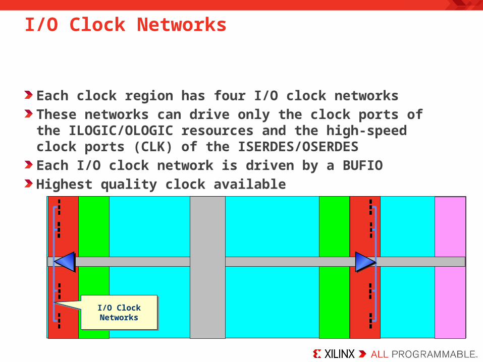
I/O Clock Networks
Each clock region has four I/O clock networks
These networks can drive only the clock ports of the ILOGIC/OLOGIC resources and the high-speed clock ports (CLK) of the ISERDES/OSERDES
Each I/O clock network is driven by a BUFIO
Highest quality clock available
I/O Clock NetworksI/O Clock Networks

I/O Clocking
The I/O clock networks are driven by the BUFIO
The BUFIO is a simple clock buffer with noadditional functionality
Driven by– Clock-capable inputs in the same I/O bank– MMCM high-performance clocks in the same region
• These are immediately adjacent to the I/O bank
– The BUFMR in the same region or region above or below– Interconnect
BUFIO
I O

Source-Synchronous Interfaces
I/O and regional clock networks combined with ISERDES/OSERDES provide powerful tools for creating source synchronous interfaces
BUFR is set to ÷N if interface is SDR, or ÷(N/2) if DDR– N can be 2 to 8 in SDR, and 2 to 14 in DDR
NISERDESISERDES
CLK CLKDIVFPGA FabricFPGA Fabric
CLK
Data
IO
CCIOBUFIO
BUFR÷

Multi-Region Clock Buffer (BUFMR)
Each bank has two BUFMRs
Allows a single clock source to be driven to the BUFIOand/or BUFR in the region above and below– Can be used to create an interface with more than 50
pins (maximum 150)
Driven by– Multi-region clock capable I/O
(MRCC) pin– Gigabit transceiver clock
Can drive only the BUFIO andBUFR in the same region, regionabove and region below
BUFMRCE
I O
CE
BUFMR
I O

Synchronizing BUFRs Driven by a BUFMR
In order to clock a single interface that spans multiple banks, a BUFMR must be used to drive the BUFIO and BUFR in the different regions
The dividers on each BUFR are independent; they must be synchronized in order to ensure proper operation of the interface– Use a BUFMRCE to disable the clock feeding the BUFRs– Assert the CLR on all the BUFRs
• This resets the dividers in the BUFRs– Deassert the CLR on all the BUFRs
• This allows the dividers to start on the nextrising edge the input clock (currently gated)
– Assert the CE on the BUFMR• Starts the clocks to all BUFRs• BUFRs are now in sync
CE
÷
÷
÷
CLR
BUFMRCE
BUFR

High-Performance Clocks
Four performance paths driving theI/O column clocked resources
Driven by– MMCM outputs O0-O3
Can drive– BUFIO– BUFR– OSERDES clocks directly
Cleanest path from MMCM to I/O columns
Lower jitter than any other routing
Software automatically places critical signals onto performance path routing
MM
CM
4

Connections to the Center Column
The BUFGCTRL and BUFH reside in the center column of the FPGA
The CCIO, BUFIO, and BUFR reside in the I/O column
The MMCM and PLL reside in the CMT column, immediately adjacent to the I/O column
GTs source clocks in the GT column
Dedicated routing pathsexist in the HCLK row tobring clocks between these resources– The tools will use these
routes when necessary
I/OCMTCLK GT

Stacked Silicon Interconnect Implications
Larger 7 series devices are made upof Super Logic Region (SLR) blocks– SLR boundaries are on clock region
boundaries
The vertical spines of the globalclock run through all SLRs– Each SLR has 32 BUFGCTRLs– Any 32 of the total number can be
used– Expect increased clock skew between SLRs—the software tools will
automatically account for this
BUFMR tracks cannot pass from one SLR to the next

7 Series FPGA Clock Network Summary
Clock regions are 50 CLBs tall
Clock regionsmatch I/O banks
50 I/Os per I/O bank
12 horizontal clock spinesand 12 BUFH
4 BUFRs and4 regional clocks
4 BUFIO and4 I/O clock networks
Clock regionsspan one half the die
4 differential or single-ended clock capable inputs

Overview
Clock Networks and Buffers
Clock Management Tile
Usage Models
Using Clock Resources
Summary
Lessons

Summary
Don’t start trying to control your design’s routing– This presentation has noted when the tools will automatically choose the
appropriate routing resources– Instantiate the appropriate primitive
Make certain you connect your Serdes clocks appropriately using the proper routing resources
Consider using area constraints to isolate logic into a single SLR, if possible– Stacked Silicon devices still have 32 global clocks

Where Can I Learn More?
User Guides – 7 Series FPGAs Clocking Resources User Guide
• Describes the complete clocking structures
Xilinx Education Services courses– www.xilinx.com/training
• Designing with the 7 Series Families course• Xilinx tools and architecture courses• Hardware description language courses• Basic FPGA architecture, Basic HDL Coding Techniques, and other Free
Videos!

Xilinx is disclosing this Document and Intellectual Property (hereinafter “the Design”) to you for use in the development of designs to operate on, or interface with Xilinx FPGAs. Except as stated herein, none of the Design may be copied, reproduced, distributed, republished, downloaded, displayed, posted, or transmitted in any form or by any means including, but not limited to, electronic, mechanical, photocopying, recording, or otherwise, without the prior written consent of Xilinx. Any unauthorized use of the Design may violate copyright laws, trademark laws, the laws of privacy and publicity, and communications regulations and statutes.
Xilinx does not assume any liability arising out of the application or use of the Design; nor does Xilinx convey any license under its patents, copyrights, or any rights of others. You are responsible for obtaining any rights you may require for your use or implementation of the Design. Xilinx reserves the right to make changes, at any time, to the Design as deemed desirable in the sole discretion of Xilinx. Xilinx assumes no obligation to correct any errors contained herein or to advise you of any correction if such be made. Xilinx will not assume any liability for the accuracy or correctness of any engineering or technical support or assistance provided to you in connection with the Design.
THE DESIGN IS PROVIDED “AS IS" WITH ALL FAULTS, AND THE ENTIRE RISK AS TO ITS FUNCTION AND IMPLEMENTATION IS WITH YOU. YOU ACKNOWLEDGE AND AGREE THAT YOU HAVE NOT RELIED ON ANY ORAL OR WRITTEN INFORMATION OR ADVICE, WHETHER GIVEN BY XILINX, OR ITS AGENTS OR EMPLOYEES. XILINX MAKES NO OTHER WARRANTIES, WHETHER EXPRESS, IMPLIED, OR STATUTORY, REGARDING THE DESIGN, INCLUDING ANY WARRANTIES OF MERCHANTABILITY, FITNESS FOR A PARTICULAR PURPOSE, TITLE, AND NONINFRINGEMENT OF THIRD-PARTY RIGHTS.
IN NO EVENT WILL XILINX BE LIABLE FOR ANY CONSEQUENTIAL, INDIRECT, EXEMPLARY, SPECIAL, OR INCIDENTAL DAMAGES, INCLUDING ANY LOST DATA AND LOST PROFITS, ARISING FROM OR RELATING TO YOUR USE OF THE DESIGN, EVEN IF YOU HAVE BEEN ADVISED OF THE POSSIBILITY OF SUCH DAMAGES. THE TOTAL CUMULATIVE LIABILITY OF XILINX IN CONNECTION WITH YOUR USE OF THE DESIGN, WHETHER IN CONTRACT OR TORT OR OTHERWISE, WILL IN NO EVENT EXCEED THE AMOUNT OF FEES PAID BY YOU TO XILINX HEREUNDER FOR USE OF THE DESIGN. YOU ACKNOWLEDGE THAT THE FEES, IF ANY, REFLECT THE ALLOCATION OF RISK SET FORTH IN THIS AGREEMENT AND THAT XILINX WOULD NOT MAKE AVAILABLE THE DESIGN TO YOU WITHOUT THESE LIMITATIONS OF LIABILITY.
The Design is not designed or intended for use in the development of on-line control equipment in hazardous environments requiring fail-safe controls, such as in the operation of nuclear facilities, aircraft navigation or communications systems, air traffic control, life support, or weapons systems (“High-Risk Applications”). Xilinx specifically disclaims any express or implied warranties of fitness for such High-Risk Applications. You represent that use of the Design in such High-Risk Applications is fully at your risk.
© 2012 Xilinx, Inc. All rights reserved. XILINX, the Xilinx logo, and other designated brands included herein are trademarks of Xilinx, Inc. All other trademarks are the property of their respective owners.
Trademark Information

7 Series Clocking Resources
Part 3

Objectives
After completing this module, you will be able to:
Specify the resources available in the Clock Management Tile (CMT)
Use the CMT resources in your design

Overview
Clock Networks and Buffers
Clock Management Tile
Usage Models
Using Clock Resources
Summary
Lessons

MMCM and PLL Features
Up to 24CMTs per device– One MMCMs and one PLL per
CMT
Two software primitives– *_BASE has only the basic ports– *_ADV provides access to all
ports
PLL is primarily intended for use withthe I/O phaser for high speed memorycontrollers
The MMCM is the primary clock resourcefor user clocks
CLKIN1CLKFBINCLKIN1CLKFBIN CLKOUT<6:0>
CLKOUTB<3:0>CLKFBOUT
CLKOUT<6:0>CLKOUTB<3:0>
CLKFBOUT
MMCME2_BASE
RSTRSTLOCKEDLOCKEDPWRDWNPWRDWN
CLKIN1CLKFBINCLKIN1CLKFBIN CLKOUT<6:0>
CLKOUTB<3:0>CLKFBOUT
CLKOUT<6:0>CLKOUTB<3:0>
CLKFBOUT
MMCME2_ADV
CLKIN2CLKINSEL
DRPPhase Shift
CLKIN2CLKINSEL
DRPPhase Shift
RSTRST
CLKINSTOPPEDCLKFBSTOPPED
LOCKED
CLKINSTOPPEDCLKFBSTOPPED
LOCKED
PWRDWNPWRDWN
CLKIN1CLKFBINCLKIN1CLKFBIN
CLKOUT<5:0>CLKFBOUT
CLKOUT<5:0>CLKFBOUT
PLLE2_BASE
RSTRST LOCKEDLOCKEDPWRDWNPWRDWN
CLKIN1CLKFBINCLKIN1CLKFBIN
CLKOUT<5:0>CLKFBOUT
CLKOUT<5:0>CLKFBOUT
PLLE2_ADV
CLKIN2CLKINSEL
DRP
CLKIN2CLKINSEL
DRP
RSTRSTLOCKEDLOCKED
PWRDWNPWRDWN

PLL Architecture
FVCO = FIN * M / D FOUT = FVCO / O = FIN * M / D / O
CLKIN1CLKIN2
D PFD
Lock DetectLock Monitor LOCKED
CP LF VCO
8-phasetaps
O0
O1
O2
O3
O4
O5
M
CLKFBIN
CLKINSEL
CLKOUT0
CLKOUT1
CLKOUT2
CLKOUT3
CLKOUT4
CLKOUT5
FIN FVCO
FOUT
FPFD
CLKFBOUT

PLL Features
Frequency lock between FPFD and CLKFB
Phase lock between CLKIN and CLKFB
Frequency synthesis for up to 6 different outputs– Fout = Fin * M / (D*O)
• One M and one D value per PLL• Each PLL output can have its own O value• M: 1-64; D: 1-56; O: 1-128
Static phase shifting increments of 1/8 of the VCO period– Each output has independent selection of the phase
Duty cycle generation in increments of 1/8 of the VCO period
Reference clock switching
Lock detectionPWRDWN signal to disable regulated power supply

Extra MMCM Features
Fractional counters– Ability to configure O0 and M as a
counter with 1/8th granularity (for example, 2.125, 2.250, 2.375, etc.)
– Enables many more VCO frequencies and output frequencies to be synthesized
Dynamic phase shifting
Fine phase shifting
Divider cascading for wider divider range – O4 divider uses resources from O6
0
45
90
135
180
225
270
315
VCOOutputs
O0
O1
O2
O3
O4
O5
O6
CLKFBOUT

Additional MMCM Signals
Complement outputs– O0-O3 of every MMCM have
both true and complement outputs
CLKOUT6 output (with O6 divider)
Dynamic phase shift port– PSCLK– PSEN– PSINCDEC– PSDONE
VCOLFCPPFD O0
CLKFB
CLKIN1CLKIN2
Routing ClockSwitch
D
CLKINSTOPPED
Lock
CLKFBSTOPPED
StopDetect
LockDetect
9
O1
O2
O3
O4
O5
O6
MCLKFBOUT
HOLD
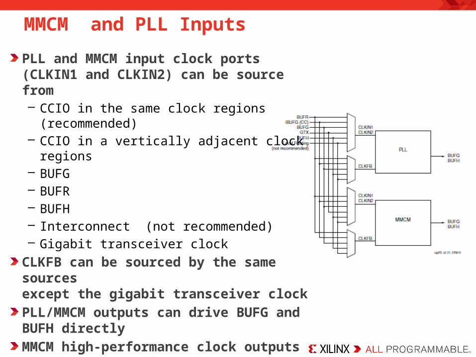
MMCM and PLL Inputs
PLL and MMCM input clock ports (CLKIN1 and CLKIN2) can be source from– CCIO in the same clock regions (recommended)– CCIO in a vertically adjacent clock regions– BUFG– BUFR– BUFH – Interconnect (not recommended)– Gigabit transceiver clock
CLKFB can be sourced by the same sourcesexcept the gigabit transceiver clock
PLL/MMCM outputs can drive BUFG and BUFH directly
MMCM high-performance clock outputs (O0 – O3) can drive BUFIO, BUFR, and CLK of OSERDES in the same region directly
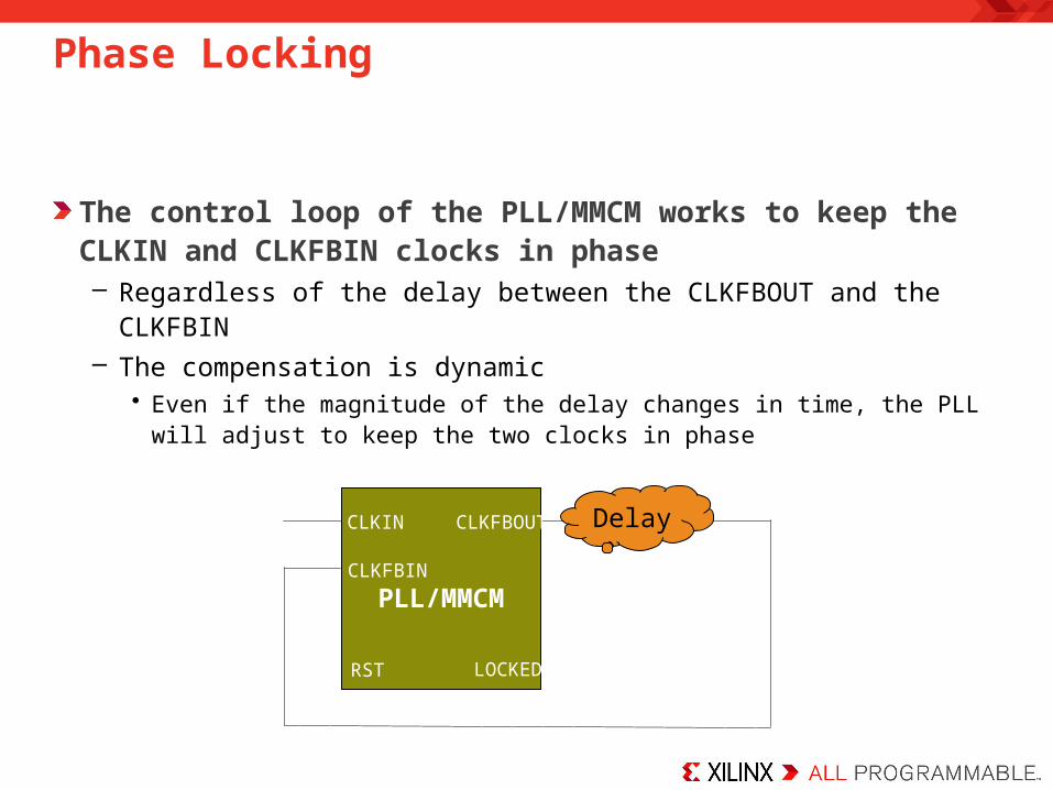
Phase Locking
The control loop of the PLL/MMCM works to keep the CLKIN and CLKFBIN clocks in phase– Regardless of the delay between the CLKFBOUT and the CLKFBIN– The compensation is dynamic
• Even if the magnitude of the delay changes in time, the PLL will adjust to keep the two clocks in phase
PLL/MMCM
CLKIN
CLKFBIN
RST
CLKFBOUT
LOCKED
Delay

Frequency Generation
The same mechanism that keeps clocks in phase generates new frequencies
By placing a divider of M between the VCO and the CLKFBOUT output, the VCO must run at M times the CLKIN frequency in order to achieve phase lock
Similarly, by placing a D divider between the CLKIN port and the PFD block, the VCO must now run at M/D times the frequency of CLKINin order to achieve phase lock
Finally, the output dividers divide the VCO frequency for the output ports
VCOLFCPPFD O0
CLKFB
CLKIN1CLKIN2
Routing ClockSwitch
D
CLKINSTOPPED
Lock
CLKFBSTOPPED
StopDetect
LockDetect
9
O1
O2
O3
O4
O5
O6
MCLKFBOUT
HOLD

Interpolated Fine Phase Shift (IFPS)
In addition to the static phase shifting capability available in the PLL and MMCM, the MMCM can also perform interpolated fine phase shifting– The VCO output can be shifted in increments of 1/56 of the VCO period– The shift amount can be set
statically or can be dynamicallycontrolled
The shifted VCO output can beselected as the input to any of the clock outputs or the CLKFBOUT output
The shift amount is 0 to 360°– The shift amount wraps around
VCO O0
O1
M
CLKOUT0
CLKOUT1
CLKFBOUT
IFPSPSINCDEC
PSENPSDONE
8

Overview
Clock Networks and Buffers
Clock Management Tile
Usage Models
Using Clock Resources
Summary
Lessons

Summary
PLL and MMCMs offer a BASE (basic ports) and ADV (all ports) primitives
VCO is the voltage controlled oscillator– Ideally, the PFD should be as high as possible (within a valid range)– If the frequency of VCO is high, you can generate more output frequencies
and you generally get better jitter performance• Higher frequencies of VCO uses more power
The MMCM also provides a fixed phase shift, interpolated phase shift, and active phase shift functionality

Where Can I Learn More?
User Guides – 7 Series FPGAs Clocking Resources User Guide
• Describes the complete clocking structures
Xilinx Education Services courses– www.xilinx.com/training
• Designing with the 7 Series Families course• Xilinx tools and architecture courses• Hardware description language courses• Basic FPGA architecture, Basic HDL Coding Techniques, and other Free
Videos!

Xilinx is disclosing this Document and Intellectual Property (hereinafter “the Design”) to you for use in the development of designs to operate on, or interface with Xilinx FPGAs. Except as stated herein, none of the Design may be copied, reproduced, distributed, republished, downloaded, displayed, posted, or transmitted in any form or by any means including, but not limited to, electronic, mechanical, photocopying, recording, or otherwise, without the prior written consent of Xilinx. Any unauthorized use of the Design may violate copyright laws, trademark laws, the laws of privacy and publicity, and communications regulations and statutes.
Xilinx does not assume any liability arising out of the application or use of the Design; nor does Xilinx convey any license under its patents, copyrights, or any rights of others. You are responsible for obtaining any rights you may require for your use or implementation of the Design. Xilinx reserves the right to make changes, at any time, to the Design as deemed desirable in the sole discretion of Xilinx. Xilinx assumes no obligation to correct any errors contained herein or to advise you of any correction if such be made. Xilinx will not assume any liability for the accuracy or correctness of any engineering or technical support or assistance provided to you in connection with the Design.
THE DESIGN IS PROVIDED “AS IS" WITH ALL FAULTS, AND THE ENTIRE RISK AS TO ITS FUNCTION AND IMPLEMENTATION IS WITH YOU. YOU ACKNOWLEDGE AND AGREE THAT YOU HAVE NOT RELIED ON ANY ORAL OR WRITTEN INFORMATION OR ADVICE, WHETHER GIVEN BY XILINX, OR ITS AGENTS OR EMPLOYEES. XILINX MAKES NO OTHER WARRANTIES, WHETHER EXPRESS, IMPLIED, OR STATUTORY, REGARDING THE DESIGN, INCLUDING ANY WARRANTIES OF MERCHANTABILITY, FITNESS FOR A PARTICULAR PURPOSE, TITLE, AND NONINFRINGEMENT OF THIRD-PARTY RIGHTS.
IN NO EVENT WILL XILINX BE LIABLE FOR ANY CONSEQUENTIAL, INDIRECT, EXEMPLARY, SPECIAL, OR INCIDENTAL DAMAGES, INCLUDING ANY LOST DATA AND LOST PROFITS, ARISING FROM OR RELATING TO YOUR USE OF THE DESIGN, EVEN IF YOU HAVE BEEN ADVISED OF THE POSSIBILITY OF SUCH DAMAGES. THE TOTAL CUMULATIVE LIABILITY OF XILINX IN CONNECTION WITH YOUR USE OF THE DESIGN, WHETHER IN CONTRACT OR TORT OR OTHERWISE, WILL IN NO EVENT EXCEED THE AMOUNT OF FEES PAID BY YOU TO XILINX HEREUNDER FOR USE OF THE DESIGN. YOU ACKNOWLEDGE THAT THE FEES, IF ANY, REFLECT THE ALLOCATION OF RISK SET FORTH IN THIS AGREEMENT AND THAT XILINX WOULD NOT MAKE AVAILABLE THE DESIGN TO YOU WITHOUT THESE LIMITATIONS OF LIABILITY.
The Design is not designed or intended for use in the development of on-line control equipment in hazardous environments requiring fail-safe controls, such as in the operation of nuclear facilities, aircraft navigation or communications systems, air traffic control, life support, or weapons systems (“High-Risk Applications”). Xilinx specifically disclaims any express or implied warranties of fitness for such High-Risk Applications. You represent that use of the Design in such High-Risk Applications is fully at your risk.
© 2012 Xilinx, Inc. All rights reserved. XILINX, the Xilinx logo, and other designated brands included herein are trademarks of Xilinx, Inc. All other trademarks are the property of their respective owners.
Trademark Information

7 Series Clocking Resources
Part 4

Objectives
After completing this module, you will be able to:
Detail the clocking resources available in the 7 series FPGAs
Specify the resources available in the Clock Management Tile (CMT)
Use the clocking resources in your design

Overview
Clock Networks and Buffers
Clock Management Tile
Usage Models
Using Clock Resources
Summary
Lessons

Clock Insertion Delay
Bringing the clock in from an IBUFG, through a BUFG, and distributing it through the global clock tree introduces delay on the clock path– Delay is Process/Voltage/Temperature (PVT) dependent– Increases setup/hold window on input flip-flops– Increases output valid uncertainty on output flip-flops– Restricts high-speed interface design using global clock resources
Clock
Required Data Valid(without clock insertion)
Required Data Valid(with clock delay)
IBUFG BUFG
IBUF
D Q
Clock Insertion Delay

IBUFG
To logic
BUFG
PLL/MMCM
CLKIN
CLKFBIN
RST
CLKFBOUT
LOCKED
Clock Insertion Delay Removal Example
The PLL/MMCM keeps CLKIN and CLKFBIN in phase, cancelling out all delay between CLKFBOUT and CLKFBIN– In this case, the delay is that of the BUFG and global clock network– The delay is cancelled regardless of PVT variation over time
Thus, the clock arriving at the logic driven by the global clock is in phase with the input clock; the clock insertion delay is removed
LOCKED

System-Synchronous Clocking
FPGA 1
IBUFG
PLL/MMCM
INFBIN
OUTBUFG
Q D
OBUF
IBUF
D Q
FPGA 2
IBUFG
PLL/MMCM
INFBIN
OUTBUFG
DQ
IBUF
OBUF
QD
CLK
Internal de-skew allows for synchronous interfaces with no hold-time violations – The tools will automatically select COMPENSATION=ZHOLD

IBUFG
CLKA (To logic)BUFG
PLL/MMCM
CLKIN
CLKFBIN
RST
CLKOUT1
LOCKED
Using Internal Feedback
When using a PLL/MMCM for frequency synthesis or jitter reduction only– Phase of CLKA has no requirements with respect to CLKIN
Tools will select the internal feedback path, which requires no routing or logic outside the PLL/MMCM– Tools will automatically set COMPENSATION=INTERNAL
LOCKED
CLKOUTFB
CLKIN
IBUFG
CLKA (To logic)BUFG
PLL/MMCM
CLKIN
CLKFBIN
RST
CLKOUT0
LOCKED
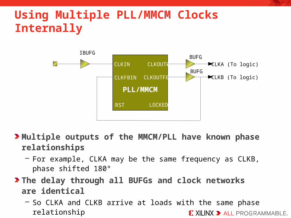
Using Multiple PLL/MMCM Clocks Internally
Multiple outputs of the MMCM/PLL have known phase relationships– For example, CLKA may be the same frequency as CLKB, phase
shifted 180°
The delay through all BUFGs and clock networks are identical– So CLKA and CLKB arrive at loads with the same phase relationship– Crossing from one clock domain to the other can be accomplished
synchronously
LOCKED
CLKOUTFB CLKB (To logic)BUFG

IBUFG BUFG
LOCKED
Clock Mirror Example
The PLL or MMCM keeps the input and feedback clock in phase– The feedback clock is not restricted to being the output of the global
clock network
In this example, two (or more) identical output clocks are generated– One is used as the feedback clock– The others are mirrors; hence, in phase with each other and the input
clock
IBUFG PLL/MMCM
CLKIN
CLKFBIN
RST
CLKOUT
LOCKED
OBUF
ODDR
OBUF
ODDR
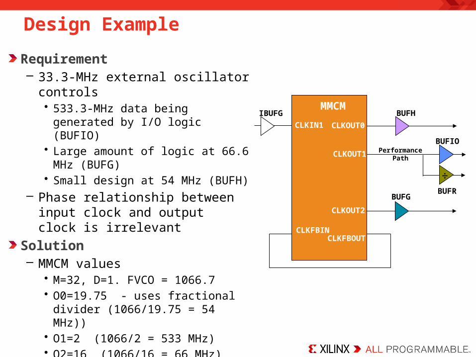
Design Example
Requirement– 33.3-MHz external oscillator controls
• 533.3-MHz data being generated by I/O logic (BUFIO)
• Large amount of logic at 66.6 MHz (BUFG)
• Small design at 54 MHz (BUFH)– Phase relationship between input
clock and output clock is irrelevant
Solution– MMCM values
• M=32, D=1. FVCO = 1066.7• O0=19.75 - uses fractional divider
(1066/19.75 = 54 MHz))• O1=2 (1066/2 = 533 MHz)• O2=16 (1066/16 = 66 MHz)
MMCM
PerformancePath
BUFIO
BUFH
BUFR
CLKIN1 CLKOUT0
CLKOUT1
CLKOUT2
CLKFBINCLKFBOUT
BUFG
÷
IBUFG

Overview
Clock Networks and Buffers
Clock Management Tile
Usage Models
Using Clock Resources
Summary
Lessons

Inference
Clock networks are represented by nets in your RTL design– The mapping of an RTL net to a clock network is managed by using
the appropriate clock buffer to generate that net
Certain resources can be inferred– A primary input net (with or without an IBUF instantiated) will be
mapped to a global clock if it drives the clock inputs of clocked resources• The BUFG will be inferred
– BUFH drivers will be inferred whenever a global clock (driven by a BUFG) is required in a clock region• BUFHs for each region required will be inferred
BUFIO, BUFR, and BUFMR cannot be inferred– Instantiating these buffers tells the tools that you want to use the
corresponding clock networks
PLLs and MMCMs cannot be inferred

Instantiation
All clocking resources can be directly instantiated in your RTL code– Simulation models exist for all resources– Refer to the Library Guide for HDL Designs– Use the Language Templates ( )
PLLs and MMCMs have many inputs and outputs, as well as many attributes– Optimal dividers for obtaining the desired characteristics may be hard to
derive– The Clocking Wizard via the CORE Generator™ interface can help

Clocking Wizard
The Clocking Wizard walks you through the generation of complete clocking subsystems– Specify the input frequency and desired output frequencies, phases and
duty cycles– Specify the desired
buffers
Chooses the optimal PLL/MMCM settings
Instantiates all clock and input buffers

Overview
Clock Networks and Buffers
Clock Management Tile
Usage Models
Using Clock Resources
Summary
Lessons

Summary
The Architecture Wizard makes it easy to build and instantiate your clocking resources– Provides instantiation template– Gui for customization of the components– Includes a jitter calculator and calculates parameter values– Application specific instantiations (such as Clock Mirror, System
Synchronous Clocking, and Feedback options)

Where Can I Learn More?
User Guides – 7 Series FPGAs Clocking Resources User Guide
• Describes the complete clocking structures
Xilinx Education Services courses– www.xilinx.com/training
• Designing with the 7 Series Families course• Xilinx tools and architecture courses• Hardware description language courses• Basic FPGA architecture, Basic HDL Coding Techniques, and other Free
Videos!

Xilinx is disclosing this Document and Intellectual Property (hereinafter “the Design”) to you for use in the development of designs to operate on, or interface with Xilinx FPGAs. Except as stated herein, none of the Design may be copied, reproduced, distributed, republished, downloaded, displayed, posted, or transmitted in any form or by any means including, but not limited to, electronic, mechanical, photocopying, recording, or otherwise, without the prior written consent of Xilinx. Any unauthorized use of the Design may violate copyright laws, trademark laws, the laws of privacy and publicity, and communications regulations and statutes.
Xilinx does not assume any liability arising out of the application or use of the Design; nor does Xilinx convey any license under its patents, copyrights, or any rights of others. You are responsible for obtaining any rights you may require for your use or implementation of the Design. Xilinx reserves the right to make changes, at any time, to the Design as deemed desirable in the sole discretion of Xilinx. Xilinx assumes no obligation to correct any errors contained herein or to advise you of any correction if such be made. Xilinx will not assume any liability for the accuracy or correctness of any engineering or technical support or assistance provided to you in connection with the Design.
THE DESIGN IS PROVIDED “AS IS" WITH ALL FAULTS, AND THE ENTIRE RISK AS TO ITS FUNCTION AND IMPLEMENTATION IS WITH YOU. YOU ACKNOWLEDGE AND AGREE THAT YOU HAVE NOT RELIED ON ANY ORAL OR WRITTEN INFORMATION OR ADVICE, WHETHER GIVEN BY XILINX, OR ITS AGENTS OR EMPLOYEES. XILINX MAKES NO OTHER WARRANTIES, WHETHER EXPRESS, IMPLIED, OR STATUTORY, REGARDING THE DESIGN, INCLUDING ANY WARRANTIES OF MERCHANTABILITY, FITNESS FOR A PARTICULAR PURPOSE, TITLE, AND NONINFRINGEMENT OF THIRD-PARTY RIGHTS.
IN NO EVENT WILL XILINX BE LIABLE FOR ANY CONSEQUENTIAL, INDIRECT, EXEMPLARY, SPECIAL, OR INCIDENTAL DAMAGES, INCLUDING ANY LOST DATA AND LOST PROFITS, ARISING FROM OR RELATING TO YOUR USE OF THE DESIGN, EVEN IF YOU HAVE BEEN ADVISED OF THE POSSIBILITY OF SUCH DAMAGES. THE TOTAL CUMULATIVE LIABILITY OF XILINX IN CONNECTION WITH YOUR USE OF THE DESIGN, WHETHER IN CONTRACT OR TORT OR OTHERWISE, WILL IN NO EVENT EXCEED THE AMOUNT OF FEES PAID BY YOU TO XILINX HEREUNDER FOR USE OF THE DESIGN. YOU ACKNOWLEDGE THAT THE FEES, IF ANY, REFLECT THE ALLOCATION OF RISK SET FORTH IN THIS AGREEMENT AND THAT XILINX WOULD NOT MAKE AVAILABLE THE DESIGN TO YOU WITHOUT THESE LIMITATIONS OF LIABILITY.
The Design is not designed or intended for use in the development of on-line control equipment in hazardous environments requiring fail-safe controls, such as in the operation of nuclear facilities, aircraft navigation or communications systems, air traffic control, life support, or weapons systems (“High-Risk Applications”). Xilinx specifically disclaims any express or implied warranties of fitness for such High-Risk Applications. You represent that use of the Design in such High-Risk Applications is fully at your risk.
© 2012 Xilinx, Inc. All rights reserved. XILINX, the Xilinx logo, and other designated brands included herein are trademarks of Xilinx, Inc. All other trademarks are the property of their respective owners.
Trademark Information