7 Clocking Strategies
8
Lecture 7 - 1 1-Feb-05 E4.20 Digital IC Design Lecture 7 Clocking Strategies in VLSI Systems Peter Cheung Department of Electrical & Electronic Engineering Imperial College London URL: www.ee.ic.ac.uk/pcheung/ E-mail: [email protected] Lecture 7 - 2 1-Feb-05 E4.20 Digital IC Design Clock - key to synchronous systems Clocks help the design of FSM where outputs depend on both input and previous states. Clock signals provide reference points in time - define what is previous state, current state and next state: Lecture 7 - 3 1-Feb-05 E4.20 Digital IC Design Latch vs Flip-Flop Lecture 7 - 4 1-Feb-05 E4.20 Digital IC Design Clock for timing synchronization Clocks serve to slow down signals that are too fast • Flip-flops / latches act as barriers • With a latch, a signal can’t propagate through until the clock is high • With a Flip-flop, the signal only propagates through on the rising edge • All real flip-flops consist of two latch like elements (master and slave latch)
-
Upload
ernest-tiong -
Category
Documents
-
view
17 -
download
1
description
Clock
Transcript of 7 Clocking Strategies
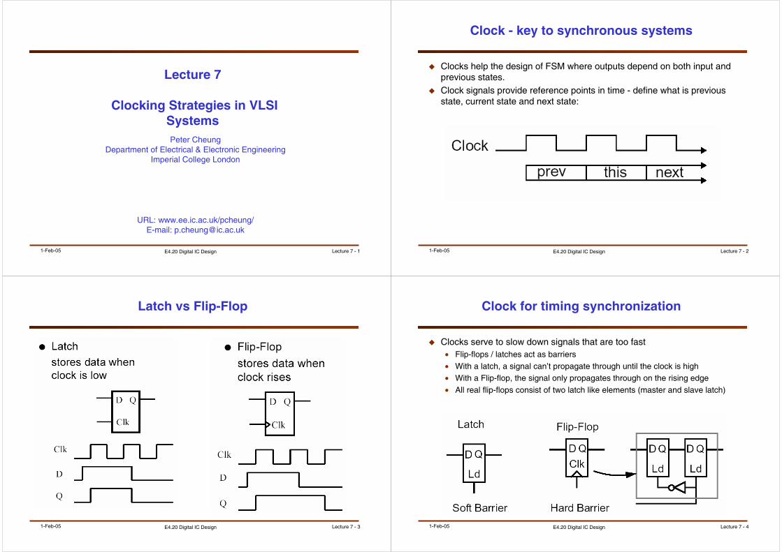
Lecture 7 - 11-Feb-05 E4.20 Digital IC Design
Lecture 7
Clocking Strategies in VLSI SystemsPeter Cheung
Department of Electrical & Electronic EngineeringImperial College London
URL: www.ee.ic.ac.uk/pcheung/E-mail: [email protected]
Lecture 7 - 21-Feb-05 E4.20 Digital IC Design
Clock - key to synchronous systems
Clocks help the design of FSM where outputs depend on both input and previous states.Clock signals provide reference points in time - define what is previous state, current state and next state:
Lecture 7 - 31-Feb-05 E4.20 Digital IC Design
Latch vs Flip-Flop
Lecture 7 - 41-Feb-05 E4.20 Digital IC Design
Clock for timing synchronization
Clocks serve to slow down signals that are too fast• Flip-flops / latches act as barriers
• With a latch, a signal can’t propagate through until the clock is high• With a Flip-flop, the signal only propagates through on the rising edge
• All real flip-flops consist of two latch like elements (master and slave latch)
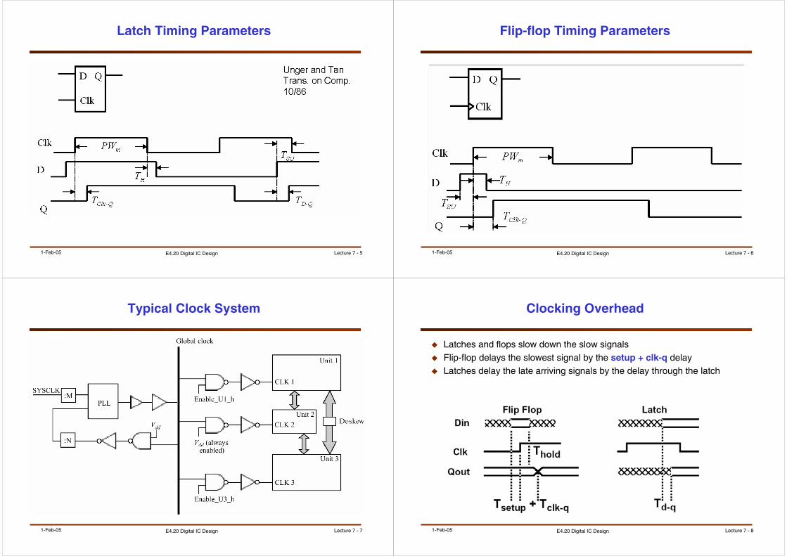
Lecture 7 - 51-Feb-05 E4.20 Digital IC Design
Latch Timing Parameters
Lecture 7 - 61-Feb-05 E4.20 Digital IC Design
Flip-flop Timing Parameters
Lecture 7 - 71-Feb-05 E4.20 Digital IC Design
Typical Clock System
Lecture 7 - 81-Feb-05 E4.20 Digital IC Design
Clocking Overhead
Latches and flops slow down the slow signalsFlip-flop delays the slowest signal by the setup + clk-q delayLatches delay the late arriving signals by the delay through the latch
Lecture 7 - 91-Feb-05 E4.20 Digital IC Design
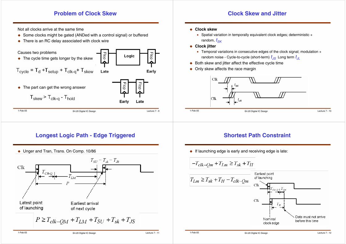
Problem of Clock Skew
Not all clocks arrive at the same timeSome clocks might be gated (ANDed with a control signal) or bufferedThere is an RC delay associated with clock wire
Causes two problemsThe cycle time gets longer by the skew
The part can get the wrong answer
Lecture 7 - 101-Feb-05 E4.20 Digital IC Design
Clock Skew and Jitter
Clock skew• Spatial variation in temporally equivalent clock edges; deterministic +
random, tSK
Clock jitter• Temporal variations in consecutive edges of the clock signal; modulation +
random noise - Cycle-to-cycle (short-term) tJS Long term tJL
Both skew and jitter affect the effective cycle timeOnly skew affects the race margin
Lecture 7 - 111-Feb-05 E4.20 Digital IC Design
Longest Logic Path - Edge Triggered
Unger and Tran, Trans. On Comp. 10/86
Lecture 7 - 121-Feb-05 E4.20 Digital IC Design
Shortest Path Constraint
If launching edge is early and receiving edge is late:

Lecture 7 - 131-Feb-05 E4.20 Digital IC Design
Clocking Strategies
Trade off between overhead / robustness / complexityConstraints on the logic vs. Constraints on the clocksLook at a number of different clocking methods:• Pulse mode clocking
• Edge triggered clocking • Two phase clocking
• Single phase clocking
We will only look at system level strategy - consider clocked circuits in the next lecture
Lecture 7 - 141-Feb-05 E4.20 Digital IC Design
Pulse Mode Clocking
Two requirements:• All loops of logic are broken by a single latch
• The clock is a narrow pulse
It must be shorter than the shortest path through the logic
Timing Requirements
Lecture 7 - 151-Feb-05 E4.20 Digital IC Design
+Pulse Mode Clocking
Used in the original Cray computers (ECL machines)Advantage is it has a very small clocking overhead• One latch delay added to cycle
Leads to double sided timing constraints• If logic is too slow OR too fast, the system will fail
Pulse width is critical• Hard to maintain narrow pulses through inverter chains
People are starting to use this type of clocking for MOS circuits• Pulse generation is done in each latch.
• Clock distributed is 50% duty cycle
• CAD tools check min delay
Not a good clocking strategy for a beginning designer
Lecture 7 - 161-Feb-05 E4.20 Digital IC Design
Edge Trigger Flip-flop
Popular TTL design styleUsed in many ASIC designs (Gate Arrays and Std Cells)Using a single clock, but replaces latches with flip-flops
Timing Constraintstdmax < tcycle - tsetup - tclk-q - tskew
tdmin > tskew + thold - tclk-q
If skew is large enough, still have two sided timing constraints

Lecture 7 - 171-Feb-05 E4.20 Digital IC Design
Two phase clocking
Use different edges for latching the data and changing the output
There are 4 different time periods, all under user control:
Φ1 highΦ 1 falling to Φ 2 risingΦ 2 highΦ 2 falling to Φ 1 rising
Lecture 7 - 181-Feb-05 E4.20 Digital IC Design
Two phase clocking
Look at shift register again:If there is a large skew on the Φ2x clock, then the spacing between Φ1 and Φ2can be increased to make sure that even with the skew, the Φ2 latch closesbefore the Φ1 latch lets the new data pass.For some setting of the timing of the clock edges, the circuit will work!
Lecture 7 - 191-Feb-05 E4.20 Digital IC Design
Stable signal type
We will give signals timing types, so it will be easier to know which latch to use:Output of a Φ1 latch is stable Φ2 (_s2) – good input to Φ2 latchOutput of a Φ2 latch is stable Φ1 (_s1) – good input to Φ1 latchSignal is called stable2, since it is stable for the entire Φ2 period
Lecture 7 - 201-Feb-05 E4.20 Digital IC Design
General two phase system
Combination logic does not change the value of timing types.No static feedback in the combination logic is allowed either. This makes the system not sensitive to logic glitches.
Lecture 7 - 211-Feb-05 E4.20 Digital IC Design
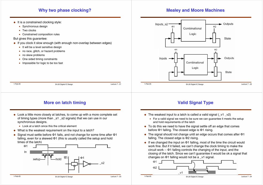
Why two phase clocking?
It is a constrained clocking style:• Synchronous design
• Two clocks• Constrained composition rules
But gives this guarantee:If you clock it slow enough (with enough non-overlap between edges)• It will be a level sensitive design
• no race, glitch, or hazard problems• no skew problems
• One sided timing constraints
• Impossible for logic to be too fast
Lecture 7 - 221-Feb-05 E4.20 Digital IC Design
Mealey and Moore Machines
Lecture 7 - 231-Feb-05 E4.20 Digital IC Design
More on latch timing
Look a little more closely at latches, to come up with a more complete set of timing types (more than _s1 _s2 signals) that we can use in our synchronous designs.• Look at a latch since this the critical element
What is the weakest requirement on the input to a latch?Signal must settle before Φ1 falls, and not change for some time after Φ1 falling, even for a skewed Φ1 (this is usually called the setup and hold times of the latch)
Lecture 7 - 241-Feb-05 E4.20 Digital IC Design
Valid Signal Type
The weakest input to a latch is called a valid signal (_v1 _v2)• For a valid signal we need to be sure we can guarantee it meets the setup
and hold requirements of the latch
To do this we need to have the signal settle off an edge that comes before Φ1 falling. The closest edge is Φ1 rising.The signal should not change until an edge occurs that comes after Φ1 falling. The closest edge is Φ2 rising.If we changed the input on Φ1 falling, most of the time the circuit would work fine. But if it failed, we can’t change the clock timing to make the circuit work -- Φ1 falling controls the changing of the input, and the closing of the latch. Since we can’t guarantee it would be ok a signal that changes on Φ1 falling would not be a _v1 signal.

Lecture 7 - 251-Feb-05 E4.20 Digital IC Design
Use of valid signal
Very useful for precharged logicIs not needed for standard combinational logic with latches• This should always give stable signals
Can’t use stable signals if you want to drive two signals/cycle on a wire (multiplex the wire), since the value has to change twice. There are many wrong ways to do it, and only one right way, which is shown below. The values become _v signals.
Lecture 7 - 261-Feb-05 E4.20 Digital IC Design
Stable Signals
Have even larger timing margins than valid signalsA _s1 signal starts to change sometime after Φ2 risesA _s1 signal settles sometime after Φ2 risesInput to the latch must be a _v2 (settles after Φ2 rises)Output of a latch settles some small delay after input settles• Please note that combinational logic does not change the value of the timing
type, even though it does increase the delay of the signal path. The timing types have to do with the clocking guarantee that we are trying to keep. This promise is that the circuit will work at some frequency. A _s1 signal might not settle until after Φ1 rises when the part is run at high-frequency, but the label means that you can make that signal stabilize before Φ1 rises if you need to by slowing the clock down.
Lecture 7 - 271-Feb-05 E4.20 Digital IC Design
Qualified (Gated) Clocks
These are signals that have the same timing as clocks, but they don’t occur every cycle. They are formed by ANDing a ‘_s1’ signal with Φ1 giving _q1, or ANDing a ‘_s2’ signal with Φ2 giving a _q2 signal.The control signal needs to be a stable signal to prevent glitches on the qualified clocks.Qualified clocks can only be used as the clock input to a latch
Lecture 7 - 281-Feb-05 E4.20 Digital IC Design
Summary of Clock Types
The figure shows the timing of all the signals we have discussed with little arrows that indication with clock edge caused the signal to change. Remember the pictures, and the timing types are what the signals look like at slow clock frequencies

Lecture 7 - 291-Feb-05 E4.20 Digital IC Design
Disadvantages of two phase clocking
Need four clocks in general• Need true and complement of both clocks
Still need low skew for good performance• The skew increases the cycle time of the machine
• Need low skew between all the clocks for good performance• Want to have Φ1 and Φ2 close to coincident
Many systems use clock and its complement instead of 2 phases• Needless to say they are very careful about clock skew• For these systems it is still useful to maintain 2 phase timing types, since it
ensures you connect all logic to the right latches• Call Clk - Φ1 and Clk - Φ2, and go from there.
• Note in this class we will use Φ1 and Φ2 for clocks)
Lecture 7 - 301-Feb-05 E4.20 Digital IC Design
Advantage of Latches Over Flip-Flops
If you are going to use Clk and Clk_b and control skew, why not go back to flip-flops?Many people do:• Most designs in industry are based on flip-flops
• Very easy to verify timing
• Each path between flip-flops must be less than cycle time• Tools check for skew and hold time violations
• Short paths are padded (buffers are added to slow down the signals)
• Skew in flip-flop based systems affects the critical path
Latch designs are more flexible than a flip-flop design• Gives the designer more rope
• Need to CAD tools to make sure it works• Can borrow time to allow a path to be longer than clock period
• Can tolerate clock skew -- skew does not directly add to cycle time
Lecture 7 - 311-Feb-05 E4.20 Digital IC Design
Single-phase Clocking
Unger and Tan, Trans. On Comp Oct 86
Lecture 7 - 321-Feb-05 E4.20 Digital IC Design
Latch-based Design with Single-phase clock