![Aiwa 6Zg-1 Video CD Mechanism Parts & Service[1]](https://static.fdocuments.in/doc/165x107/55cf9737550346d033904ea0/aiwa-6zg-1-video-cd-mechanism-parts-service1.jpg)
6ZG-1
22
SERVICE MANUAL DATA 6ZG-1 English CD-R/RW MECHANISM BASIC CD MECHANISM :3ZG-2 E2 TYPE SRTDM S/M Code No. 09-001-338-7N6
Transcript of 6ZG-1

SERVICE MANUAL
DATA
6ZG-1 English
CD-R/RW MECHANISM BASIC CD MECHANISM :3ZG-2 E2
TYPE
SRTDM
S/M Code No. 09-001-338-7N6

2
PROTECTION OF EYES FROM LASER BEAM DURING SERVICING
VAROITUS!Laiteen Käyttäminen muulla kuin tässä käyttöohjeessa mainit-
ulla tavalla saattaa altistaa käyt-täjän turvallisuusluokan 1 ylit-
tävälle näkymättömälle lasersäteilylle.
VARNING!Om apparaten används på annat sätt än vad som specificeras i
denna bruksanvising, kan användaren utsättas för osynling
laserstrålning, som överskrider gränsen för laserklass 1.
Caution: Invisible laser radiation when
open and interlocks defeated avoid expo-
sure to beam.
Advarsel:Usynling laserståling ved åbning,
når sikkerhedsafbrydere er ude af funktion.
Undgå udsættelse for stråling.
CAUTIONUse of controls or adjustments or performance of procedures
other than those specified herein may result in hazardous
radiation exposure.
ATTENTIONL'utilisation de commandes, réglages ou procédures autres que
ceux spécifiés peut entraîner une dangereuse exposition aux
radiations.
ADVARSEL!Usynlig laserståling ved åbning, når sikkerhedsafbrydereer ude
af funktion. Undgå udsættelse for stråling.
This Compact Disc player is classified as a CLASS 1 LASER
product.
The CLASS 1 LASER PRODUCT label is located on the rear
exterior.
This set employs laser. Therefore, be sure to follow carefully the
instructions below when servicing.
WARNING!WHEN SERVICING, DO NOT APPROACH THE LASER EXIT
WITH THE EYE TOO CLOSELY. IN CASE IT IS NECESSARY TO
CONFIRM LASER BEAM EMISSION. BE SURE TO OBSERVE
FROM A DISTANCE OF MORE THAN 30cm FROM THE
SURFACE OF THE OBJECTIVE LENS ON THE OPTICAL
PICK-UP BLOCK.
CLASS 1KLASSE 1LUOKAN 1KLASS 1
LASER PRODUCTLASER PRODUKTLASER LAITELASER APPARAT
Precaution to replace Optical block(KSS-213F)
1) After the connection, remove solder shown inthe right figure.
Body or clothes electrostatic potential could ruinlaser diode in the optical block. Be sure groundbody and workbench, and use care the clothesdo not touch the diode.

3
1. How to replace PICK UP.1) Open the TRAY.
Push the stopper to arrow direction and release half ofthe SHAFT SLED.
2) Turn GEAR MAIN CAM to the counterclockwise(arrow “a”) direction, and lift up CD mechanism. (Fig-1)
3) Remove SHAFT SLED.4) CD mechanism in down position, replace PICK UP.5) Lift up CD mechanism (Fig-1), and Reassemble the
SHAFT SLED.
2. How to remove the 5CD CHANGER BLOCK(Fig-2)1) Remove the two FFC of the CD circuit board, and
remove the five SCREWS.2) Lift 5 CD CHANGER BLOCK from behind, and
remove it. (5CD CHANGER BLOCK can be removedeven if PANEL TRAY is not removed.)
DISASSEMBLY INSTRUCTIONS
STOPPER
a
GEAR MAIN CAM
SHAFT SLED
PICKUP
FFC
FFC SCREW5CD CHANGER BLOCK
LIFT UP
Fig-1
Fig-2

4
3. The disassemble and reassemble the TRAY3-1. Disassembling procedure.
1) Push the PLATE GEAR’S Boss at the bottom part ofCHAS MECHA strongly to the outside (arrow “b”direction). (Fig-3)(Confirm that TRAY appears a little in the front.)
2) Draw TRAY to the open position.3) Remove FFC, and push the two LEVERS at both side of
the CHAS MECH to remove TRAY. (Fig-4)
3-2. Reassembling procedure.
1) Confirm that LEVER TRAY is at the most right positionand check for the CD Mechanism to be in the downposition. (Fig-5)
2) Push in the TRAY along the rail of the CHAS MECHA.
5CD CHANGER BLOCK
BOSS
b
FFC
Fig-3
LEVER TRY
TRAY
FFC
Fig-5 Fig-6
Fig-4
LEVER
LEVER
TRAY
3) After TRAY is half closed and FFC is put in, it can enterby force until the end of TRAY closed. (Fig-6)

5
4. How to reassemble the TURN TABLE. (Fig-7)1) Push LEVER TT in the direction of “C”, and put in the
TURN TABLE 5CD. (Fig-7)After reassembly, one of the TURN TABLE DISCTRAY (can be either one of the five disc trays) must bealigned with TURN TABLE 5CD. (Fig-8)That is, having no gap difference between the TURNTABLE 5CD and the TRAY 5CD.
* When reassembling the TURN TABLE 5CD, it isacceptable facing any CD number (1-5).
ALIGN
TURN TABLE 5CD
TRAY 5CD
Fig-7 Fig-8
C LEVER TT

6
REF. NO PART NO. KANRI DESCRIPTIONNO.
REF. NO PART NO. KANRI DESCRIPTIONNO.
ELECTRICAL MAIN PARTS LIST
IC
87-A20-547-010 C-IC,CXA1992AR 87-017-917-080 IC,BU4066BCF 87-A20-546-010 C-IC,CXD2589Q 87-A20-592-040 C-IC,M51943 AML 87-A21-428-040 C-IC,NJM2115M
87-070-305-010 IC,BA6897S 87-001-982-010 IC,TA7291S
TRANSISTOR
87-026-463-080 TR,2SA933S (0.3W) 89-324-123-080 C-TR,2SC2412K S 87-026-227-080 CHIP-TR,DTA114EK 89-421-722-380 TR,2SD2172V/W 89-320-011-080 TR,2SC2001 (15W)
87-026-239-080 TR,DTC114TK (0.2W) 87-A30-031-010 P-TR,PT380F 89-110-155-080 TR,2SA1015(0.4W) 87-026-608-080 C-TR,DTC 123 JK 87-A30-075-080 C-TR,2SA1235F
DIODE
87-020-465-080 DIODE,1SS133 (110MA)
5CD C.B
C101 87-010-263-040 CAP,E 100-10 C102 87-010-178-080 CHIP CAP 1000P C103 87-010-550-040 CAP,E 100-6.3 GAS C104 87-010-182-080 C-CAP,S 2200P-50 B C105 87-010-198-080 CAP, CHIP 0.022
C106 87-016-081-080 C-CAP,S 0.1-16 RK C107 87-016-081-080 C-CAP,S 0.1-16 RK C108 87-016-081-080 C-CAP,S 0.1-16 RK C109 87-010-497-040 CAP,E 4.7-35 GAS C110 87-016-081-080 C-CAP,S 0.1-16 RK
C111 87-010-197-080 CAP, CHIP 0.01 DM C112 87-010-417-040 CAP,E 2.2-35 5L C113 87-015-678-040 CAP,E 22-10 M 7L SRA C114 87-010-213-080 C-CAP,S 0.015-50 B C115 87-010-060-040 CAP,E 100-16
C116 87-010-197-080 CAP, CHIP 0.01 DM C117 87-010-186-080 CAP,CHIP 4700P C118 87-010-197-080 CAP, CHIP 0.01 DM C119 87-016-369-080 C-CAP,S 0.033-25 B K C120 87-010-197-080 CAP, CHIP 0.01 DM
C121 87-010-494-040 CAP,E 1-50 GAS C122 87-010-152-080 C-CAP,S 8P-50 CH C123 87-010-154-080 CAP CHIP 10P C124 87-010-154-080 CAP CHIP 10P C125 87-010-596-080 CAP, S 0.047-16
C126 87-010-596-080 CAP, S 0.047-16 C127 87-012-140-080 CAP 470P C128 87-010-596-080 CAP, S 0.047-16 C129 87-010-198-080 CAP, CHIP 0.022 C130 87-016-081-080 C-CAP,S 0.1-16 RK
C131 87-010-550-040 CAP,E 100-6.3 GAS C132 87-010-550-040 CAP,E 100-6.3 GAS C133 87-012-158-080 C-CAP,S 390P-50 CH C140 87-010-805-080 CAP, S 1-16 C151 87-012-156-080 C-CAP,S 220P-50 CH
C202 87-010-596-080 CAP, S 0.047-16 C203 87-010-188-080 CAP,CHIP 6800P C204 87-012-156-080 C-CAP,S 220P-50 CH C205 87-018-133-080 CAPACITOR,CER 4700P-16V C206 87-016-526-080 C-CAP,S 0.47-16 BK
C207 87-010-197-080 CAP, CHIP 0.01 DM
C208 87-010-318-080 C-CAP,S 47P-50 CH C209 87-012-154-080 C-CAP,S 150P-50 CH C210 87-012-154-080 C-CAP,S 150P-50 CH C211 87-010-176-080 C-CAP,S 680P-50 SL C212 87-010-176-080 C-CAP,S 680P-50 SL
C213 87-015-678-040 CAP,E 22-10 M 7L SRA C214 87-015-678-040 CAP,E 22-10 M 7L SRA C215 87-010-318-080 C-CAP,S 47P-50 CH C216 87-010-318-080 C-CAP,S 47P-50 CH C217 87-010-078-040 CAP,E 47-6.3 5L
C218 87-010-197-080 CAP, CHIP 0.01 DM C219 87-010-196-080 CHIP CAPACITOR,0.1-25 C220 87-010-370-040 CAP,E 330-6.3 SME C221 87-010-197-080 CAP, CHIP 0.01 DM C222 87-010-186-080 CAP,CHIP 4700P
C223 87-016-081-080 C-CAP,S 0.1-16 RK C230 87-018-209-080 CAP, CER 0.1-50V C231 87-018-209-080 CAP, CER 0.1-50V C301 87-010-101-080 CAP, ELECT 220-16 C302 87-010-060-080 ELECTROLYTIC 100-16V
C305 87-010-318-080 C-CAP,S 47P-50 CH C306 87-010-318-080 C-CAP,S 47P-50 CH C307 87-010-075-080 CAP,10U-16V H5 C308 87-010-075-080 CAP,10U-16V H5 C401 87-010-073-080 CAP,E 3.3-50 5L
C402 87-010-073-040 CAP,E 3.3-50 5L C403 87-018-134-080 CAPACITOR,TC-U 0.01-16 C501 87-016-459-040 CAP,E 470-10 SMG C502 87-010-197-080 CAP, CHIP 0.01 DM C503 87-010-060-040 CAP,E 100-16
C504 87-010-196-080 CHIP CAPACITOR,0.1-25 C505 87-010-196-080 CHIP CAPACITOR,0.1-25 C506 87-010-196-080 CHIP CAPACITOR,0.1-25 C507 87-010-196-080 CHIP CAPACITOR,0.1-25 C508 87-016-459-040 CAP,E 470-10 SMG
C509 87-010-196-080 CHIP CAPACITOR,0.1-25 C510 87-010-196-080 CHIP CAPACITOR,0.1-25 C601 87-010-197-080 CAP, CHIP 0.01 DM C602 87-016-251-040 CAP,E 220-16 SMG C603 87-010-196-080 CHIP CAPACITOR,0.1-25
C701 87-010-322-080 C-CAP,S 100P-50 CH C702 87-010-318-080 C-CAP,S 47P-50 CH C703 87-010-318-080 C-CAP,S 47P-50 CH C705 87-010-178-080 CHIP CAP 1000P C901 87-010-078-080 CAP,E 47-6.3 5L
C902 87-010-196-080 CHIP CAPACITOR,0.1-25 CON101 87-A60-424-010 CONN,16P V TOC-B CON102 87-A60-623-010 CONN,6P V 2MM JMT CON301 87-009-346-010 CONN,3P PH H CON302 87-009-350-010 CONN,7P PH H
CON601 87-A60-133-010 CONN,8P V FE CON702 87-A60-154-010 CONN,6P H FE FB301 87-008-372-080 FILTER, EMI BL OIRNI FB401 87-008-372-080 FILTER, EMI BL OIRNI L101 87-003-102-080 COIL, 10UH
L201 87-003-102-080 COIL, 10UH LED411 87-070-288-010 LED,GL380 LED901 87-A40-558-010 LED,SLZ-8128A-01-A M601 87-045-305-010 MOTOR, RF-500TB DC-5V (2MA) R132 83-212-863-080 C-RES,S 27K-1/10W F
R133 83-212-863-080 C-RES,S 27K-1/10W F R134 83-212-863-080 C-RES,S 27K-1/10W F R135 83-212-863-080 C-RES,S 27K-1/10W F R136 87-022-360-080 C-RES,S 39K-1/10WF R137 87-022-360-080 C-RES,S 39K-1/10WF
R138 87-022-364-080 C-RES,S 82K-1/10W F R139 87-022-364-080 C-RES,S 82K-1/10W F R140 87-022-202-080 C-RES,S33K 1/10WF R141 87-022-202-080 C-RES,S33K 1/10WF R301 87-025-337-080 RESISTOR, 1/4W 47
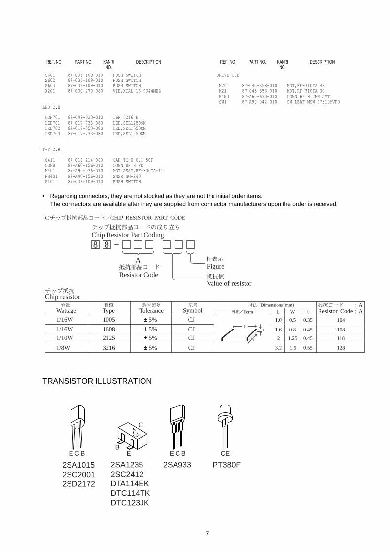
7
REF. NO PART NO. KANRI DESCRIPTIONNO.
REF. NO PART NO. KANRI DESCRIPTIONNO.
TRANSISTOR ILLUSTRATION
8 8
A
Resistor Code
Chip Resistor Part Coding
Figure
Value of resistor
Chip resistor
Wattage Type Tolerance
1/16W
1/10W
1/8W
1608
2125
3216
5%
5%
5%
CJ
CJ
CJ
Form L W t
1.6 0.8 0.45
2 1.25 0.45
3.2 1.6
108
118
128
: A : A
CHIP RESISTOR PART CODE
0.55
Resistor CodeDimensions (mm)
Symbol
1/16W 1005 5% CJ 1.0 0.5 0.35 104L
t
W
EB
C
E C B E C B
2SA12352SC2412DTA114EKDTC114TKDTC123JK
2SA10152SC20012SD2172
2SA933
CE
PT380F
S601 87-036-109-010 PUSH SWITCH S602 87-036-109-010 PUSH SWITCH S603 87-036-109-010 PUSH SWITCH X201 87-030-270-080 VIB,XTAL 16.9344MHZ
LED C.B
CON701 87-099-033-010 16P 6216 H LED701 87-017-733-080 LED,SEL1250SM LED702 87-017-350-080 LED,SEL1550CM LED703 87-017-733-080 LED,SEL1250SM
T-T C.B
C411 87-018-214-080 CAP TC U 0.1-50F CON8 87-A60-156-010 CONN,8P H FE M401 87-A90-036-010 MOT ASSY,RF-300CA-11 PS401 87-A90-156-010 SNSR,SG-240 S401 87-036-109-010 PUSH SWITCH
DRIVE C.B
M20 87-045-358-010 MOT,RF-310TA 43 M21 87-045-356-010 MOT,RF-310TA 30 PIN3 87-A60-670-010 CONN,6P H 2MM JMT SW1 87-A90-042-010 SW,LEAF MSW-17310MVP0
• Regarding connectors, they are not stocked as they are not the initial order items.The connectors are available after they are supplied from connector manufacturers upon the order is received.
8
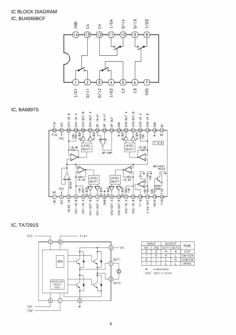
IC BLOCK DIAGRAM
IC, BA6897S
IC, TA7291S
PROTECTORCIRCUIT
(TSD)
STOP
BRAKE
: HI IMPEDANCE
NOTE : INPUT “H” ACTIVE
IC, BU4066BCF

109
BLOCK DIAGRAM
Q401-404
TO
MA
IN U
NIT
TO
MA
IN U
NIT
CON8

1 2 3 4 5 6 7 8 9 10 11 12 13 14
A
B
C
D
E
F
G
H
I
J
K
1211
WIRING-1 (5CD/LED)
TO T-T C.BCON8

1413
SCHEMATIC DIAGRAM
BIA
S

1615
1 2 3 4 5 6 7
A
B
C
D
E
F
G
H
I
J
K
WIRING-2 (T-T/DRIVE)
TO 5CD C.BCON601
TO 5CD C.BCON102
DRIVEC.B
1 IC201 Pin , (XTAI, XTAO) VOLT/DIV: 2VSYSTEM CLOCK TIME/DIV: 0.1µSf=16.9344MHz
2 TP1 (TP-RF) VOLT/DIV: 500mVRF TIME/DIV: 0.5µS
3 IC101 Pin 6 (FE O) VOLT/DIV: 200mVFOCUS TIME/DIV: 2mS
WAVE FORM
4.2V
0
4 IC101 Pin # (TA O) TIME/DIV: 1mSTRACKING
5 IC101 Pin 1 (FE O)FOCUS SEARCH
VC
VCCD: 1.0±0.1VCD-RW: 0.9±0.1V
VC
70 71

17
Pressing the [E] key decreases the track number to -1.Pressing the [F] key increases the track number to +1.Pressing OPEN/CLOSE key opens or closes the tray.The machine enters the [Sled mode].
< How to Exit the Test Mode >
Remove the AC power cord from power outlet, or turnoff the system power.
The focus bias, tracking balance and the tracking gainadjustment values can be displayed, modified, set andreleased in the Play mode only of the following Testmode.When the PRGM button is pressed during Play, theadjustment value of the focus bias is displayed. Afterthat, you can enter the followings:
• FOCUS - BIAS
[Display]: Pressing the PRGM key during disc play, thefocus bias setting value is displayed.[Adjustment]: Every pressing of the fi key decrementsthe adjustment value by 1 step.Every pressing of the fl key increments the adjustmentvalue by 1 step.[Set]: The adjustment value is set by pressing the PLAYkey after adjustment. Playback a disc after setting.[Release]: The set value can be released by pressing theSTOP key.
• TRACKING - BALANCE
[Display]: Pressing the REPEAT key during disc play,the tracking balance setting value is displayed.[Adjustment]: The same procedure as in the FOCUS -BIAS.[Set]: The same procedure as in the FOCUS - BIAS.[Release]: The same procedure as in the FOCUS - BIAS.
• TRACKING - GAIN
[Display]: Pressing the DISPLAY key during disc play,the tracking balance setting value is displayed.[Adjustment]: The same procedure as in the FOCUS -BIAS.[Set]: The same procedure as in the FOCUS - BIAS.[Release]: The same procedure as in the FOCUS - BIAS.
Display method
8 8 8-8 8: 8 8• FOCUS - BIAS
F -8 8• TRACKING - BALANCE
L-8 8• TRACKING - GAIN
G A-8 8
< How to Enter the Test Mode >
While pressing the SLEEP key, insert the AC power cordto AC wall outlet.
< When the Machine Has Entered the TestMode >
The system is initialized and the main power is turned on.During the test mode, the main power of the CD block isturned on always. The test mode starts with the [Sledmode].
< Types of Test Mode >
[Sled mode]
All displays of the FL tubes light. The optical pickup canbe moved by pressing [E] or [F] key.
Pressing the [2] key establishes the [Play mode].
Pressing the [E] key moves the sled to outercircumference.Pressing the [F] key moves the sled to innercircumference.Pressing OPEN/CLOSE key opens or closes the tray.
Lighting of all displays of the FL tubes are turned off andreturns to normal display. The focus search is performedin the focus mode regardless whether disc is inserted ornot, or focus OK or NG. (Numbers of times of focussearch is unlimited. Auto sequence is not used.)Focus servo is not locked in even the focus is obtained.
Pressing the [2] key establishes the [Play mode].Pressing the [E] key decreases the track number to -1.Pressing the [F] key increases the track number to +1.Pressing OPEN/CLOSE key opens or closes the tray.The machine enters the [Sled mode].
[Play mode]
Lighting of all displays of the FL tubes are turned off andreturns to normal display. The focus search (numbers ofsearch is unlimited) is performed. When focus comes toin-focus, the focus servo is locked in and the machinesenters the normal play mode.During [Play mode], GFS and sound skipping are notmonitored.When focus becomes out-of-focus, another attempt ismade to search for focus.The tracking servo and the sled servo can be turned onand off by pressing the [2] key.
Pressing the [9] key establishes the [Sled mode].The [ || ] display can be turned on and off by pressingthe [2] key .
While the [ || ] display is turned off:CLV-A Tracking servo: on
Sled servo: onWhile the [ || ] display is turned on:CLV-A Tracking servo: off
Sled servo: off
TEST MODE
18
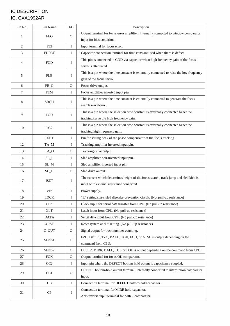
Output terminal for focus error amplifier. Internally connected to window comparator
input for bias condition.
Input terminal for focus error.
Capacitor connection terminal for time constant used when there is defect.
This pin is connected to GND via capacitor when high frequency gain of the focus
servo is attenuated.
This is a pin where the time constant is externally connected to raise the low frequency
gain of the focus servo.
Focus drive output.
Focus amplifier inverted input pin.
This is a pin where the time constant is externally connected to generate the focus
search waveform.
This is a pin where the selection time constant is externally connected to set the
tracking servo the high frequency gain.
This is a pin where the selection time constant is externally connected to set the
tracking high frequency gain.
Pin for setting peak of the phase compensator of the focus tracking.
Tracking amplifier inverted input pin.
Tracking drive output.
Sled amplifier non-inverted input pin.
Sled amplifier inverted input pin.
Sled drive output.
The current which determines height of the focus search, track jump and sled kick is
input with external resistance connected.
Power supply.
“L” setting starts sled disorder-prevention circuit. (Not pull-up resistance)
Clock input for serial data transfer from CPU. (No pull-up resistance)
Latch input from CPU. (No pull-up resistance)
Serial data input from CPU. (No pull-up resistance)
Reset system at “L” setting. (No pull-up resistance)
Signal output for track number counting.
FZC, DFCT1, TZC, BALH, TGH, FOH, or ATSC is output depending on the
command from CPU.
DFCT2, MIRR, BALL, TGL or FOL is output depending on the command from CPU.
Output terminal for focus OK comparator.
Input pin where the DEFECT bottom hold output is capacitance coupled.
DEFECT bottom-hold output terminal. Internally connected to interruption comparator
input.
Connection terminal for DEFECT bottom-hold capacitor.
Connection terminal for MIRR hold-capacitor.
Anti-reverse input terminal for MIRR comparator.
FEO
FEI
FDFCT
FGD
FLB
FE_O
FEM
SRCH
TGU
TG2
FSET
TA_M
TA_O
SL_P
SL_M
SL_O
ISET
Vcc
LOCK
CLK
XLT
DATA
XRST
C_OUT
SENS1
SENS2
FOK
CC2
CC1
CB
CP
IC, CXA1992AR
Pin No. Pin Name I/O Description
1
2
3
4
5
6
7
8
9
10
11
12
13
14
15
16
17
18
19
20
21
22
23
24
25
26
27
28
29
30
31
O
I
I
I
I
O
I
I
I
I
I
I
O
I
I
O
I
I
I
I
I
I
I
O
O
O
O
I
O
I
I
IC DESCRIPTION

19
RF_I
RF_O
RF_M
RFTC
LD
PD
PD1, PD2
FEBIAS
F, E
EI
VEE
TEO
LPFI
TEI
ATSC
TZC
TDFCT
VC
FZC
Pin No. Pin Name I/O Description
32
33
34
35
36
37
38, 39
40
41, 42
43
44
45
46
47
48
49
50
51
52
I
O
I
I
O
I
I
I/O
I
—
—
O
I
I
I
I
I
O
I
Input terminal by capacity combination of RF summing amplifier.
Output terminal of RF summing amplifier. Checkpoint of Eye pattern.
Anti-reverse input terminal for RF summing amplifier.
The gain of RF amplifier is decided by the connection resistance between RF_M and
RFO terminals.
This is a pin where the selection time constant is externally connected to control the
RF level.
APC amplifier output terminal.
APC amplifier input terminal.
RFI-V amplifier inverted input pin.
These pins are connected to the A+C and B+C pins of the optical pickup, receiving by
currents input.
Bias adjustment pin of the focus error amplifier. (Not connected)
F and EIV amplifier inverted input pins.
These pins are connected to the F and E of the optical pickup, receiving by current
input.
Gain adjustment pin of the I-V amplifier E. (When not in use of BAL automatic
adjustment)
GND connection pin.
Output terminal for tacking-error amplifier. Output E-F signal.
BAL adjustment comparator input pin. (Input through LPF from TEO)
Input terminal for tracking error.
Window-comparator input terminal for detecting ATSC.
Input terminal for tracking-zero cross comparator.
Capacitor connection pin for the time constant used when there is defect.
Output terminal for DC voltage reduced to half of VCC+VEE.
Input terminal for focus-zero cross comparator.
20
GND.
Lch-“0” detect flag. (Not connected)
Rch-“0” detect flag. (Not connected)
Clock input for SQSO read out.
SubQ 80 bit serial output.
SENS signal output to CPU.
Serial data input from CPU.
Latch input from CPU, Latch serial data at fall down.
Clock input to serial data transfer from CPU.
SENS input from SSP.
Numbers of track jump are counted and input.
Serial data output to SSP.
Serial-data latch output to SSP. Latch at fall down.
Clock output for serial data transfer to SSP.
Microcomputer expansion interface. (Input A)
Microcomputer expansion interface. (Input B)
Microcomputer expansion interface. (Output)
Focus OK input terminal. Used for SENS output and servo-auto sequencer.
Power supply. (+5V)
Servo control for spindle motor.
External control input for spindle motor. (Not connected)
TEST terminal. (Connected to GND)
Charge pump output for extensive EFM PLL.
VCO2 oscillator input for extensive EFM PLL.
VCO2 oscillator output for extensive EFM PLL.
VCO2 control voltage input for extensive EFM PLL.
Charge pump output for master PLL.
Filter (slave = digital PLL) output for master PLL.
Filter input for master PLL.
Analog GND.
VCO control voltage input for master.
Analog power. (+5V)
EFM signal input.
Constant current input to asymmetry circuit.
Comparison voltage input to asymmetry circuit.
EFM full-swing output. (L=VSS, H=VDD)
D/A interface, LR clock output f=FS.
LR clock input.
D/A interface, serial data output. (2’s COMP, MSB first)
D/A interface, serial data input. (2’s COMP, MSB first)
VSS
LMUT
RMUT
SQCK
SQSO
SENS
DATA
XLAT
CLOK
SEIN
CNIN
DATO
XLTO
CLKO
SPOA
SPOB
XLON
FOK
VDD
MDP
PWMI
TEST
TESI
VPCO
VCKI
V16M
VCTL
PCO
FILO
FILI
AVSS
CLTV
AVDD
RF
BIAS
ASYI
ASYO
LRCK
LRCKI
PCMD
PCMDI
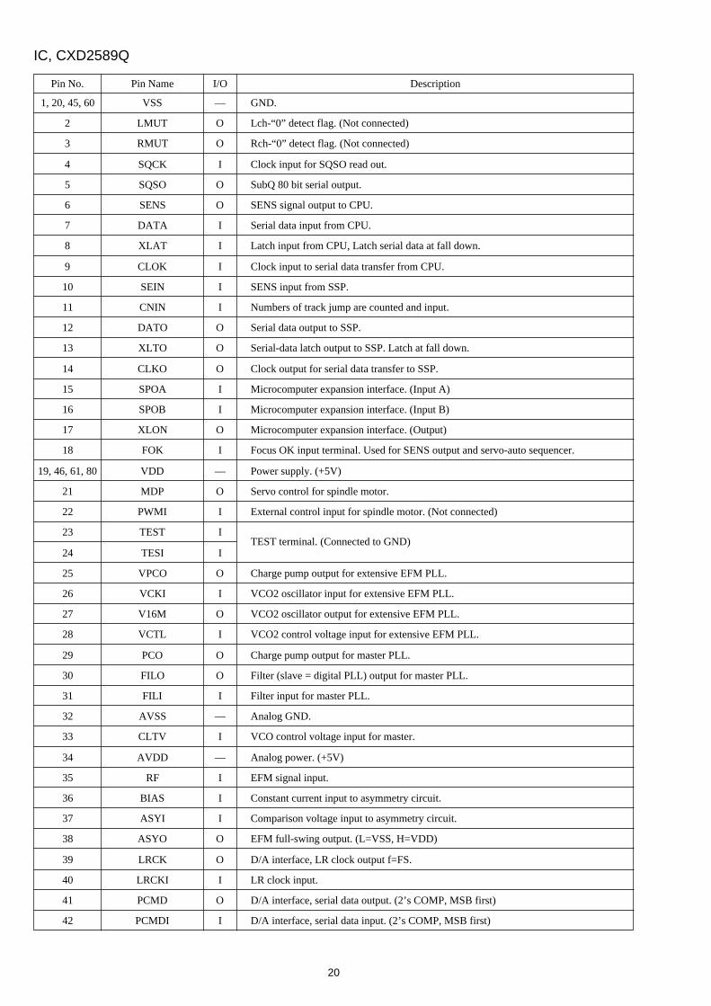
IC, CXD2589Q
Pin No. Pin Name I/O Description
1, 20, 45, 60
2
3
4
5
6
7
8
9
10
11
12
13
14
15
16
17
18
19, 46, 61, 80
21
22
23
24
25
26
27
28
29
30
31
32
33
34
35
36
37
38
39
40
41
42
—
O
O
I
O
O
I
I
I
I
I
O
O
O
I
I
O
I
—
O
I
I
I
O
I
O
I
O
O
I
—
I
—
I
I
I
O
O
I
O
I

21
D/A interface bit clock output.
D/A interface bit clock input.
XUGF output, MNT1 or RPCK output by switching command. (Not connected)
XPLCK output, MNT0 output by switching command. (Not connected)
GFS output, MNT3 or XRAOF output by switching command.
C2PO output, GTOP output by switching command. (Not connected)
X’tal select input terminal, X’tal: 16.9344MHz = “L” 33.8688MHz = “H”.
4.2336MHz output, Output 1/4 divided frequency of VCKI at CAV-W mode.
(Not connected)
Digital Out connector output signal.
“H” when the playback disc has emphasis. “L” when it does not.
De-emphasis ON/OFF, “H” when ON, “L” when OFF.
WFCK output. (Not connected)
H output when the subcode sync S0 or S1 is detected. (Not connected)
Serial output for SubP-W. (Not connected)
SBSO read out clock input.
Mute input terminal, Active the “H” setting.
Analogue GND.
Analogue power supply. (+5V)
Lch/analogue output terminal.
Lch/OP AMP input terminal.
Lch/LINE output terminal.
Analogue GND.
Power supply for master clock.
Input terminal for crystal oscillator circuit.
Input external master clock from this terminal.
Output terminal for crystal oscillator circuit.
GND terminal for master clock.
Analogue GND.
Rch/LINE output terminal.
Rch/OP AMP input terminal.
Rch/analogue output terminal.
Analogue power supply. (+5V)
Analogue GND.
Reset system at “L” setting.
BCK
BCKI
XUGF
XPCK
GFS
C2PO
XTSL
C4M
DOUT
EMPH
EMPHI
WFCK
SCOR
SESO
EXCK
SYSM
AVSS
AVDD
AOUT1
AIN1
LOUT1
AVSS
XVDD
XTAI
XTAO
XVSS
AVSS
LOUT2
AIN2
AOUT2
AVDD
AVSS
XRST
Pin No. Pin Name I/O Description
43
44
47
48
49
50
51
52
53
54
55
56
57
58
59
62
63
64
65
66
67
68
69
70
71
72
73
74
75
76
77
78
79
O
I
O
O
O
O
I
O
O
O
I
O
O
O
I
I
—
—
O
I
O
—
—
I
O
—
—
O
I
O
—
—
I
Note)• PCMD is the two’s complement output with MSB first.• GTOP monitors the protection status of the Frame Sync. (H: Sync protection window opened).• XUGF is the Frame Sync negative pulse which is obtained from the EFM signal. This is the signal before the sync protection.• XPLCK is the inverted signal of the EFM PLL clock. The PLL works so that the fall-down edge and the changed point of the
EFM signal agree.• GFS is the signal that goes “H” when the Frame Sync and the internally inserted timing agree.• RFCK is the signal having 136 micro-seconds (during normal speed) that is generated to have the same accuracy as X’tal.• C2PO is the signal indicating the error status of the data.• XRAOF is the signal that is generated when the 16k RAM goes outside the jitter margin ±4F.

22
MECHANICAL EXPLODED VIEW 1/1
1
39
38D
37
3635
3433
234
5
6
7
8
42
9A
44
43
47
CUSH CD A3ZG-2 E2
32
31
46
48
3029
AZA6
P.C.B
28
41
26
25
27
B
40
P.C.B
21
2324
22
20
16
19 18
17
15
45
14
1312
11
10A
C
D
E
P.C.B

23
REF. NO PART NO. KANRI DESCRIPTIONNO.
REF. NO PART NO. KANRI DESCRIPTIONNO.
MECHANICAL PARTS LIST 1/1
Basic color symbol Color Basic color symbol Color Basic color symbol ColorB Black C Cream D OrangeG Green H Gray L BlueLT Transparent Blue N Gold P PinkR Red S Silver ST Titan SilverT Brown V Violet W White
WT Transparent White Y Yellow YT Transparent YellowLM Metallic Blue LL Light Blue GT Transparent GreenLD Dark Blue DT Transparent Orange
COLOR NAME TABLE
1 86-ZG1-001-410 TRAY,5CD 2 84-ZG1-267-010 PULLEY,LOAD MO 8 3 87-A90-036-010 MOT ASSY,RF-300CA-11 4 86-ZG1-228-110 GEAR,TT-B 5 86-ZG1-227-110 GEAR,TT-A
6 86-ZG1-223-110 GEAR,WORM-WHEEL TT 7 86-ZG1-224-110 LEVER,TT(*) 8 86-ZG1-226-010 SPR-E,LEVER TT 9 86-ZG1-002-210 TURN TABLE,5CD 10 86-ZG1-211-210 JOINT,CAM
11 86-ZG1-216-010 SPR-E,JT 12 86-ZG1-203-210 GEAR,MAIN CAM 13 86-ZG1-213-110 LEVER,LOAD 14 86-ZG1-214-110 LEVER,PROTECT 15 86-ZG1-004-010 REFLECTOR,CD
16 86-ZG1-205-110 GEAR,TRAY 17 84-ZG1-207-010 PULLEY,RELAY 18 84-ZG1-209-010 BELT,SQ1.8-117.7 19 86-ZG1-217-010 LEVER,SW 20 86-ZG1-206-110 GEAR,RELAY B
21 86-ZG1-220-110 SPR-P,LOCK 22 86-ZG1-204-110 GEAR,RELAY A 23 86-ZG1-218-110 PLATE,GEAR 24 86-ZG1-208-010 LEVER,TRAY 25 86-ZG1-209-110 SLIDER,CAM L(*)
26 86-ZG1-210-110 SLIDER,CAM R(*) 27 84-ZG1-244-310 CABI,OPTICAL 28 84-ZG2-228-010 PULLEY,MOT 29 83-ZG3-211-010 PLATE,DISC 30 83-ZG3-604-010 RING,MAG 2
31 86-ZG1-215-010 HLDR,CHUCK 32 86-ZG1-238-010 HLDR,MAGNET 6ZG N 33 86-ZG1-225-010 BELT,SQ1.2-32.9 34 86-ZG1-221-010 PULLEY,TT 35 86-ZG1-231-010 SPR-C,WORM
36 84-ZG1-256-010 GEAR,WORM N2 37 86-ZG1-232-010 SPR-P,WORM 38 86-ZG1-229-010 HLDR,SENSOR 39 86-ZG1-230-010 HLDR,DISC SENSOR 40 86-ZG1-240-210 CHAS,MECHA T2
41 86-ZG1-005-110 COVER,CHAS 42 86-ZG1-003-110 COVER,TRAY 43 86-ZG1-609-010 CONN ASSY,6P 44 86-ZG1-202-210 HLDR,MECHA 45 86-ZG1-212-410 SLIDER,LOAD
46 86-ZG1-239-110 PLATE,DISC 47 86-ZG1-605-010 CABLE,FFC 16P 48 86-ZG1-667-010 F-CABLE,8P 1.25 175MM BLACK A 87-078-148-010 VFT2+3-12(F10) BLK B 87-251-072-410 U+2.6-5
C 81-ZG1-254-010 S-SCREW,MECH HLDR D 87-067-579-010 TAPPING SCREW, BVT2+3-8 E 87-067-703-010 TAPPING SCREW, BVT2+3-10

24
CD MECHANISM EXPLODED VIEW 1/1
CD MECHANISM PARTS LIST 1/1
REF. NO PART NO. KANRI DESCRIPTIONNO.
1 83-ZG2-246-310 CHAS ASSY,SHT 5 2 83-ZG2-235-010 GEAR,A3 3 83-ZG2-205-210 GEAR,B 4 83-ZG2-236-010 GEAR,MOTOR 3 5 83-ZG2-253-110 SHAFT,SLIDE 5
6 87-A90-836-010 PICKUP,KSS-213F 7 83-ZG2-254-010 TURN TABLE,C5 8 83-ZG2-245-510 LEVER,SHUTTER(*) 9 83-ZG2-250-110 SPR-E,SHT 2 A 87-261-032-210 V+2-3
P.C.B
1
7
4
2
3
5
6
M20 M21
SW1
AA
AA
89

25
ELECTRICAL SECTIONDESCRIPTION REFERENCE NAME
ANT ANTENNASC- CHIPC-CAP CAP, CHIPC-CAP TN CAP, CHIP TANTALUMC-COIL COIL, CHIP
C-DI DIODE, CHIPC-DIODE DIODE, CHIPC-FET FET, CHIPC-FOTR FILTER, CHIPC-JACK JACK, CHIP
C-LED LED, CHIPC-RES RES, CHIPC-SFR SFR, CHIPC-SLIDE SW SLIDE SWITCH, CHIPC-SW SWITCH, CHIP
C-TR TRANSISTOR, CHIPC-VR VOLUME, CHIPC-ZENER ZENER, CHIPCAP, CER CAP, CERA-SOLCAP, E CAP, ELECT
CAP, M/F CAP, FILMCAP, TC CAP, CERA-SOLCAP, TC-U CAP, CERA-SOL SSCAP, TN CAP, TANTALUMCERA FIL FILTER, CERAMIC
CF FILTER, CERAMICDL DELAY LINEE/CAP CAP, ELECTFILT FILTERFLTR FILTER
FUSE RES RES, FUSEMOT MOTORP-DIODE PHOTO DIODEP-SNSR PHOTO SENSERP-TR PHOTO TRANSISTOR
POLY VARI VARIABLE CAPACITORPPCAP CAP, PPPT POWER TRANSFORMERPTR, RES PTR, MELFRC REMOTE CONTROLLER
RES NF RES, NON-FLAMMABLERESO RESONATORSHLD SHIELDSOL SOLENOIDSPKR SPEAKER
SW, LVR SWITCH, LEVERSW, RTRY SWITCH, ROTARYSW, SL SWITCH, SLIDETC CAP CAP, CERA-SOLTHMS THERMISTOR
TR TRANSISTORTRIMMER CAP, TRIMMERTUN-CAP VARIABLE CAPACITORVIB, CER RESONATOR, CERAMICVIB, XTAL RESONATOR, CRYSTAL
VR VOLUMEZENER DIODE, ZENER
REFERENCE NAME LISTMECHANICAL SECTIONDESCRIPTION REFERENCE NAME
ADHESHIVE SHEET ADHESHIVEAZ AZIMUTHBAR-ANT BAR-ANTENNABAT BATTERYBATT BATTERY
BRG BEARINGBTN BUTTONCAB CABINETCASS CASSETTECHAS CHASSIS
CLR COLLARCONT CONTROLCRSR CURSORCU CUSHIONCUSH CUSHION
DIR DIRECTIONDUBB DUBBINGFL FRONT LOADINGFLY-WHL FLYWHEELFR FRONT
FUN FUNCTIONG-CU G-CUSHIONHDL HANDOLHIMERON CLOTHHINGE, BAT HINGE, BATTERY
HLDR HOLDERHT-SINK HEAT SINKIB INSTRUCTION BOOKLETIDLE IDLERIND, L-R INDICATOR, L-R
KEY, CONT KEY, CONTROLKEY, PRGM KEY, PROGRAMKNOB, SL KNOB, SLIDELBL LABELLID, BATT LID, BATTERY
LID, CASS LID, CASSETTELVR LEVERP-SP P-SPRINGPANEL, CONT PANEL, CONTROLPANEL, FR PANEL, FRONT
PRGM PROGRAMPULLY, LOAD MO PULLY, LOAD MOTORRBN RIBBONS- SPECIALSEG SEGMENT
SH SHEETSHLD-SH SHIELD-SHEETSL SLIDESP SPRINGSP-SCREW SPECIAL-SCREW
SPACER, BAT SPACER, BATTERYSPR SPRINGSPR-P P-SPRINGSPR-PC-PUSH P-SPRING, C-PUSHT-SP T-SPRING
TERM TERMINALTRIG TRIGGERTUN TUNINGVOL VOLUMEW WASHER
WHL WHEELWORM-WHL WORM-WHEEL

2–11, IKENOHATA 1–CHOME, TAITO-KU, TOKYO 110, JAPAN TEL:03 (3827) 3111
0251431 Printed in Singapore
![089 ' # '6& *#0 & 7 · 2018. 4. 1. · 1 1 ¢ 1 1 1 ï1 1 1 1 ¢ ¢ð1 1 ¢ 1 1 1 1 1 1 1ýzð1]þð1 1 1 1 1w ï 1 1 1w ð1 1w1 1 1 1 1 1 1 1 1 1 ¢1 1 1 1û](https://static.fdocuments.in/doc/165x107/60a360fa754ba45f27452969/089-6-0-7-2018-4-1-1-1-1-1-1-1-1-1-1-1-1-1.jpg)


![1 1 1 1 1 1 1 ¢ 1 , ¢ 1 1 1 , 1 1 1 1 ¡ 1 1 1 1 · 1 1 1 1 1 ] ð 1 1 w ï 1 x v w ^ 1 1 x w [ ^ \ w _ [ 1. 1 1 1 1 1 1 1 1 1 1 1 1 1 1 1 1 1 1 1 1 1 1 1 1 1 1 1 ð 1 ] û w ü](https://static.fdocuments.in/doc/165x107/5f40ff1754b8c6159c151d05/1-1-1-1-1-1-1-1-1-1-1-1-1-1-1-1-1-1-1-1-1-1-1-1-1-1-w-1-x-v.jpg)


![$1RYHO2SWLRQ &KDSWHU $ORN6KDUPD +HPDQJL6DQH … · 1 1 1 1 1 1 1 ¢1 1 1 1 1 ¢ 1 1 1 1 1 1 1w1¼1wv]1 1 1 1 1 1 1 1 1 1 1 1 1 ï1 ð1 1 1 1 1 3](https://static.fdocuments.in/doc/165x107/5f3ff1245bf7aa711f5af641/1ryho2swlrq-kdswhu-orn6kdupd-hpdqjl6dqh-1-1-1-1-1-1-1-1-1-1-1-1-1-1.jpg)


![1 $SU VW (G +LWDFKL +HDOWKFDUH %XVLQHVV 8QLW 1 X ñ 1 … · 2020. 5. 26. · 1 1 1 1 1 x 1 1 , x _ y ] 1 1 1 1 1 1 ¢ 1 1 1 1 1 1 1 1 1 1 1 1 1 1 1 1 1 1 1 1 1 1 1 1 1 1 1 1 1 1](https://static.fdocuments.in/doc/165x107/5fbfc0fcc822f24c4706936b/1-su-vw-g-lwdfkl-hdowkfduh-xvlqhvv-8qlw-1-x-1-2020-5-26-1-1-1-1-1-x.jpg)