6.976 High Speed Communication Circuits and Systems … · M.H. Perrott MIT OCW Frequency...
49
6.976 High Speed Communication Circuits and Systems Lecture 16 Noise in Integer-N Frequency Synthesizers Michael Perrott Massachusetts Institute of Technology Copyright © 2003 by Michael H. Perrott
Transcript of 6.976 High Speed Communication Circuits and Systems … · M.H. Perrott MIT OCW Frequency...

6.976High Speed Communication Circuits and Systems
Lecture 16Noise in Integer-N Frequency Synthesizers
Michael PerrottMassachusetts Institute of Technology
Copyright © 2003 by Michael H. Perrott

M.H. Perrott MIT OCW
Frequency Synthesizer Noise in Wireless Systems
Synthesizer noise has a negative impact on system- Receiver – lower sensitivity, poorer blocking performance- Transmitter – increased spectral emissions (output spectrum must meet a mask requirement)
Noise is characterized in frequency domain
Zin
Zo LNA To Filter
From Antennaand Bandpass
Filter
PC boardtrace
PackageInterface
LO signal
MixerRF in IF out
FrequencySynthesizer
ReferenceFrequency
VCO
f
PhaseNoise
fo

M.H. Perrott MIT OCW
Noise Modeling for Frequency Synthesizers
PLL has an impact on VCO noise in two ways- Adds extrinsic noise from various PLL circuits- Highpass filters VCO noise through PLL feedback dynamics
Focus on modeling the above based on phase deviations- Simpler than dealing directly with PLL sine wave output
vin(t)vc(t)
vn(t)
PLL dynamicsset VCO
carrier frequency f
PhaseNoise
fo
Sout(f)
Extrinsic noise(from PLL)
out(t)
Intrinsicnoise
To PLL

M.H. Perrott MIT OCW
vin(t)vc(t)
vn(t)
PLL dynamicsset VCO
carrier frequency f
PhaseNoise
fo
Frequency-domain viewSout(f)
Extrinsic noise(from PLL)
Intrinsicnoise
2πKvs
Φout
Φvn(t)
2cos(2πfot+Φout(t))out(t)
To PLL
Phase Deviation Model for Noise Analysis
Model the impact of noise on instantaneous phase- Relationship between PLL output and instantaneous phase
- Output spectrum (from Lecture 12)
Note: Kv units are Hz/V

M.H. Perrott MIT OCW
Phase noise is non-periodic
- Described as a spectral density relative to carrier power
Spurious noise is periodic
- Described as tone power relative to carrier power
Phase Noise Versus Spurious Noise
SΦout(f)Sout(f)
f-fo fo
1dBc/Hz
Sout(f)
f-fo fo
dBc1
fspur
21 dspur
fspur
2

M.H. Perrott MIT OCW
Sources of Noise in Frequency Synthesizers
Extrinsic noise sources to VCO- Reference/divider jitter and reference feedthrough- Charge pump noise
PFD ChargePump
e(t) v(t)
N
LoopFilter
DividerVCO
ref(t)
div(t)
f
Charge PumpNoise
VCO Noise
f
-20 dB/dec
1/Tf
ReferenceJitter
f
ReferenceFeedthrough
T
f
DividerJitter

M.H. Perrott MIT OCW
Modeling the Impact of Noise on Output Phase of PLL
Determine impact on output phase by deriving transfer function from each noise source to PLL output phase- There are a lot of transfer functions to keep track of!
Φdiv[k]
Φref [k] KV
jf
v(t) Φout(t)H(f)
1N
�πα e(t)
espur(t)Φjit[k] Φvn(t)Ιcpn(t)
Icp
VCO Noise
f0
SΦjit(f)
f0
SΙcpn(f)
f0
SEspur(f)
Divider/ReferenceJitter
ReferenceFeedthrough
Charge PumpNoise
1/T f0
SΦvn(f)
-20 dB/dec
PFDChargePump
LoopFilter
Divider
VCO
M.H. Perrott MIT OCW
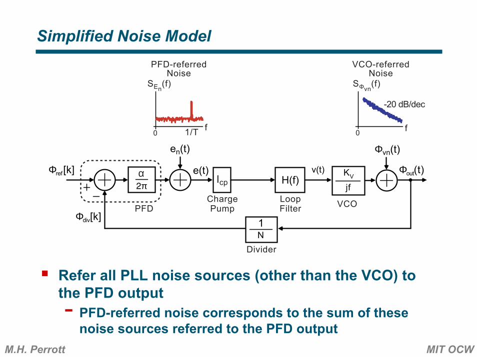
Simplified Noise Model
Refer all PLL noise sources (other than the VCO) to the PFD output- PFD-referred noise corresponds to the sum of these
noise sources referred to the PFD output
Φdiv[k]
Φref [k] KV
jf
v(t) Φout(t)H(f)
1N
�πα e(t)
Φvn(t)en(t)
Icp
VCO-referredNoise
f0
SEn(f)
PFD-referredNoise
1/T f0
SΦvn(f)
-20 dB/dec
PFDChargePump
LoopFilter
Divider
VCO

M.H. Perrott MIT OCW
Impact of PFD-referred Noise on Synthesizer Output
Transfer function derived using Black’s formula
Φdiv[k]
Φref [k] KV
jf
v(t) Φout(t)H(f)
1N
�πα e(t)
Φvn(t)en(t)
Icp
VCO-referredNoise
f0
SEn(f)
PFD-referredNoise
1/T f0
SΦvn(f)
-20 dB/dec
PFDChargePump
LoopFilter
Divider
VCO

M.H. Perrott MIT OCW
Impact of VCO-referred Noise on Synthesizer Output
Transfer function again derived from Black’s formula
Φdiv[k]
Φref [k] KV
jf
v(t) Φout(t)H(f)
1N
�πα e(t)
Φvn(t)en(t)
Icp
VCO-referredNoise
f0
SEn(f)
PFD-referredNoise
1/T f0
SΦvn(f)
-20 dB/dec
PFDChargePump
LoopFilter
Divider
VCO

M.H. Perrott MIT OCW
A Simpler Parameterization for PLL Transfer Functions
Define G(f) as
- A(f) is the open loop transfer function of the PLL
Φdiv[k]
Φref [k] KV
jf
v(t) Φout(t)H(f)
1N
�πα e(t)
Φvn(t)en(t)
Icp
VCO-referredNoise
f0
SEn(f)
PFD-referredNoise
1/T f0
SΦvn(f)
-20 dB/dec
PFDChargePump
LoopFilter
Divider
VCO
Always has a gainof one at DC

M.H. Perrott MIT OCW
Parameterize Noise Transfer Functions in Terms of G(f)
PFD-referred noise
VCO-referred noise

M.H. Perrott MIT OCW
Parameterized PLL Noise Model
PFD-referred noise is lowpass filteredVCO-referred noise is highpass filteredBoth filters have the same transition frequency values- Defined as fo
Φvn(t)en(t)
Φout(t)Φc(t)Φn(t)
Φnvco(t)Φnpfd(t)
fo1-G(f)
foG(f)�πNα
VCO-referredNoise
f0
SEn(f)
PFD-referredNoise
1/T f0
SΦvn(f)
-20 dB/dec
Divider Controlof Frequency Setting
(assume noiseless for now)
M.H. Perrott MIT OCW
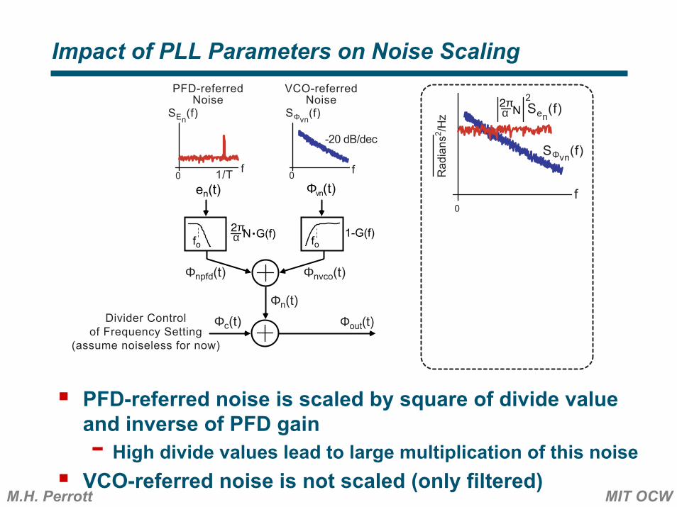
Impact of PLL Parameters on Noise Scaling
PFD-referred noise is scaled by square of divide value and inverse of PFD gain- High divide values lead to large multiplication of this noise
VCO-referred noise is not scaled (only filtered)
Φvn(t)en(t)
Φout(t)Φc(t)Φn(t)
Φnvco(t)Φnpfd(t)
fo1-G(f)
foG(f)�πNα
VCO-referredNoise
f0
SEn(f)
PFD-referredNoise
1/T f0
SΦvn(f)
-20 dB/dec
Divider Controlof Frequency Setting
(assume noiseless for now)
Sen(f)�πNα
2
Rad
ians
2 /Hz
SΦvn(f)
f0

M.H. Perrott MIT OCW
Optimal Bandwidth Setting for Minimum Noise
Optimal bandwidth is where scaled noise sources meet- Higher bandwidth will pass more PFD-referred noise- Lower bandwidth will pass more VCO-referred noise
Φvn(t)en(t)
Φout(t)Φc(t)Φn(t)
Φnvco(t)Φnpfd(t)
fo1-G(f)
foG(f)�πNα
VCO-referredNoise
f0
SEn(f)
PFD-referredNoise
1/T f0
SΦvn(f)
-20 dB/dec
Divider Controlof Frequency Setting
(assume noiseless for now)
Sen(f)�πNα
2
Rad
ians
2 /Hz
SΦvn(f)
f(fo)opt0

M.H. Perrott MIT OCW
Resulting Output Noise with Optimal Bandwidth
PFD-referred noise dominates at low frequencies- Corresponds to close-in phase noise of synthesizer
VCO-referred noise dominates at high frequencies- Corresponds to far-away phase noise of synthesizer
Φvn(t)en(t)
Φout(t)Φc(t)Φn(t)
Φnvco(t)Φnpfd(t)
fo1-G(f)
foG(f)�πNα
VCO-referredNoise
f0
SEn(f)
PFD-referredNoise
1/T f0
SΦvn(f)
-20 dB/dec
Divider Controlof Frequency Setting
(assume noiseless for now)
Sen(f)�πNα
2
Rad
ians
2 /Hz
SΦvn(f)
f(fo)opt0
Rad
ians
2 /Hz SΦnpfd(f)
SΦnvco(f)
f(fo)opt0
M.H. Perrott MIT OCW
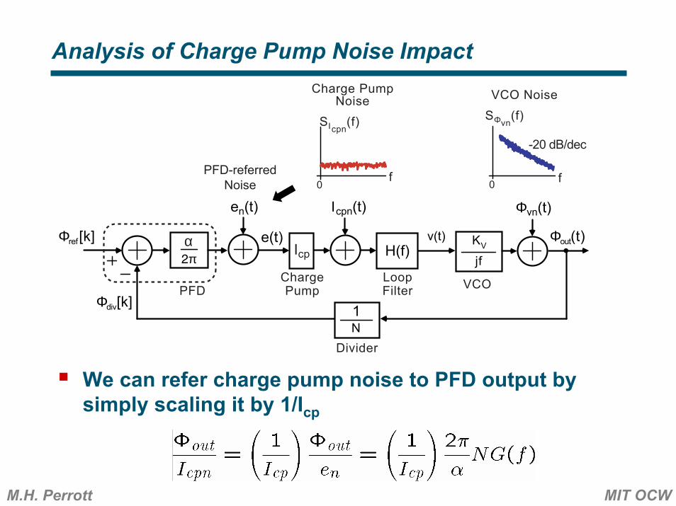
Analysis of Charge Pump Noise Impact
We can refer charge pump noise to PFD output by simply scaling it by 1/Icp
Φdiv[k]
Φref [k] KV
jf
v(t) Φout(t)H(f)
1N
�πα e(t)
en(t) Φvn(t)Ιcpn(t)
Icp
VCO Noise
f0
SΙcpn(f)
Charge PumpNoise
f0
SΦvn(f)
-20 dB/dec
PFDChargePump
LoopFilter
Divider
VCO
PFD-referredNoise

M.H. Perrott MIT OCW
Calculation of Charge Pump Noise Impact
Contribution of charge pump noise to overall output noise
- Need to determine impact of Icp on SIcpn(f)
Φdiv[k]
Φref [k] KV
jf
v(t) Φout(t)H(f)
1N
�πα e(t)
en(t) Φvn(t)Ιcpn(t)
Icp
VCO Noise
f0
SΙcpn(f)
Charge PumpNoise
f0
SΦvn(f)
-20 dB/dec
PFDChargePump
LoopFilter
Divider
VCO
PFD-referredNoise

M.H. Perrott MIT OCW
Impact of Transistor Current Value on its Noise
Charge pump noise will be related to the current it creates as
Recall that gdo is the channel resistance at zero Vds- At a fixed current density, we have
M2M1
Ibias
currentsource
current bias
Id
idbias2 id
2
Cbig
WL
M.H. Perrott MIT OCW
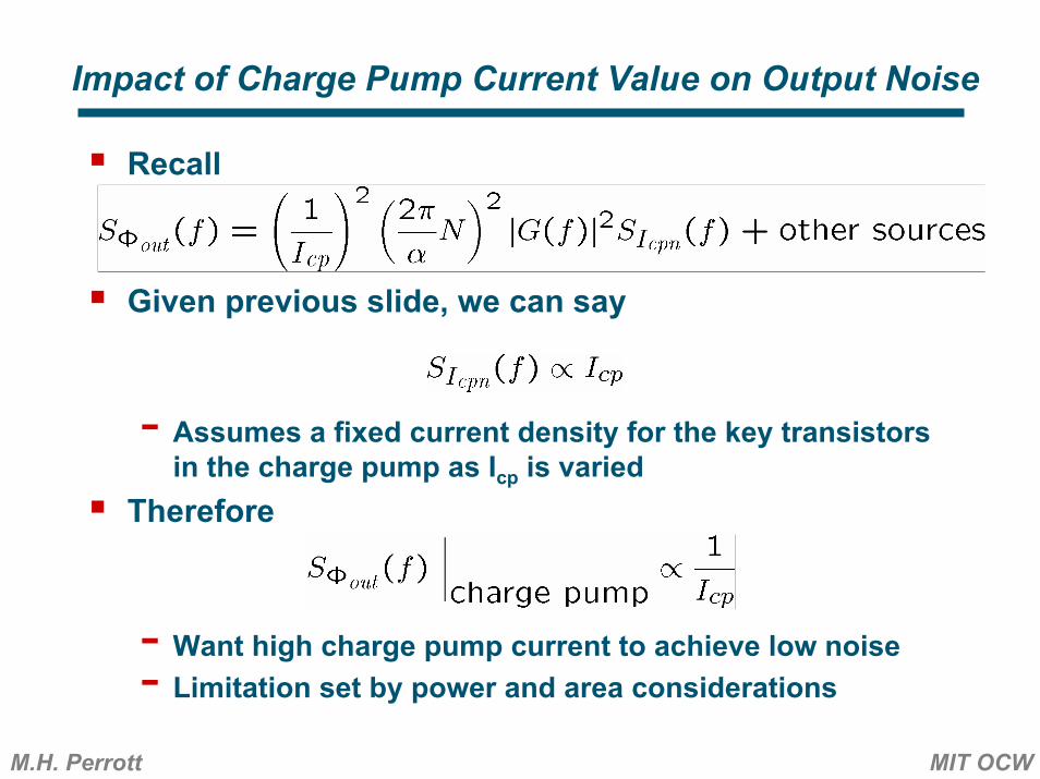
Impact of Charge Pump Current Value on Output Noise
Recall
Given previous slide, we can say
- Assumes a fixed current density for the key transistors in the charge pump as Icp is varied
Therefore
- Want high charge pump current to achieve low noise- Limitation set by power and area considerations

M.H. Perrott MIT OCW
Impact of Synthesizer Noise on Transmitters
Synthesizer noise can be lumped into two categories- Close-in phase noise: reduces SNR of modulated signal- Far-away phase noise: creates spectral emissions outside
the desired transmit channelThis is the critical issue for transmitters
Sx(f)
f
Sout(f)
ffLO
Sy(f)
ffRFfIF
x(t) y(t)
out(t)
Synthesizer
close-inphase noise
far-awayphase noise
reductionof SNR
out-of-bandemission

M.H. Perrott MIT OCW
Impact of Remaining Portion of Transmitter
Power amplifier- Nonlinearity will increase out-of-band emission and create
harmonic contentBand select filter- Removes harmonic content, but not out-of-band emission
Sx(f)
f
Sout(f)
ffLO
Sy(f)
ffRFfIF
x(t) y(t)
out(t)
Synthesizer
close-inphase noise
far-awayphase noise
reductionof SNR
out-of-bandemission
To Antenna
Band SelectFilter
PA

M.H. Perrott MIT OCW
Why is Out-of-Band Emission A Problem?
Near-far problem- Interfering transmitter closer to receiver than desired
transmitter- Out-of-emission requirements must be stringent to
prevent complete corruption of desired signal
Transmitter 2 Base
Station
Transmitter 1
Desired Channel( )
Interfering Channel( )
Relative PowerDifference (dB)
Desired Channel
Interfering Channel

M.H. Perrott MIT OCW
Specification of Out-of-Band Emissions
Maximum radiated power is specified in desired and adjacent channels- Desired channel power: maximum is M0 dBm- Out-of-band emission: maximum power defined as
integration of transmitted spectral density over bandwidth R centered at midpoint of each channel offset
ffRF
MaximumRF OutputEmission
(dBm) M0 dBm
M1 dBmM2 dBm
Channel Spacing= W Hz
IntegrationBandwidth= R Hz
M3 dBm

M.H. Perrott MIT OCW
Calculation of Transmitted Power in a Given Channel
For simplicity, assume that the spectral density is flat over the channel bandwidth- Actual spectral density of signal often varies with
frequency over the bandwidth of a given channelResulting power calculation (single-sided Sx(f))
Express in dB ( Note: dB(x) = 10log(x) )
R Hz R Hz
fmid
Sx(fmid) Sx(fmid)
fmid

M.H. Perrott MIT OCW
Transmitter Output Versus Emission Specification
Assume a piecewise constant spectral density profile for transmitter- Simplifies calculations
Issue: emission specification is measured over a narrower band than channel spacing- Need to account for bandwidth discrepancy when doing
calculations
ffRF
RF Output(dBm)
Y0 dBm
Y0+X1 dBmY0+X2 dBm
ffRF
MaximumRF OutputEmission
(dBm) M0 dBm
M1 dBmM2 dBm
M3 dBm
Channel Spacing= W Hz
Channel Spacing= W Hz
ChannelSpacing= W Hz
IntegrationBandwidth= R Hz
Y0+X3 dBm
Piecewise Constant Approximationof Transmitter Output Spectrum Emission Specification

M.H. Perrott MIT OCW
Correction Factor for Bandwidth Mismatch
Calculation of maximum emission in offset channel 1
ffRF
RF Output(dBm)
Y0 dBm
Y0+X1 dBmY0+X2 dBm
ffRF
MaximumRF OutputEmission
(dBm) M0 dBm
M1 dBmM2 dBm
M3 dBm
Channel Spacing= W Hz
Channel Spacing= W Hz
ChannelSpacing= W Hz
IntegrationBandwidth= R Hz
Y0+X3 dBm
Piecewise Constant Approximationof Transmitter Output Spectrum Emission Specification

M.H. Perrott MIT OCW
Out-of-band emission requirements are function of the power of the signal in the desired channel- For offset channel 1 (as calculated on previous slide)
- Most stringent case is when Y0 maximum
Condition for Most Stringent Emission Requirement
ffRF
RF Output(dBm)
Y0 dBm
Y0+X1 dBmY0+X2 dBm
ffRF
MaximumRF OutputEmission
(dBm) M0 dBm
M1 dBmM2 dBm
M3 dBm
Channel Spacing= W Hz
Channel Spacing= W Hz
ChannelSpacing= W Hz
IntegrationBandwidth= R Hz
Y0+X3 dBm
Piecewise Constant Approximationof Transmitter Output Spectrum Emission Specification

M.H. Perrott MIT OCW
Table of Most Stringent Emission Requirements
ffRF
RF Output(dBm)
Y0 dBm
Y0+X1 dBmY0+X2 dBm
ffRF
MaximumRF OutputEmission
(dBm) M0 dBm
M1 dBmM2 dBm
M3 dBm
Channel Spacing= W Hz
Channel Spacing= W Hz
ChannelSpacing= W Hz
IntegrationBandwidth= R Hz
Y0+X3 dBm
Piecewise Constant Approximationof Transmitter Output Spectrum Emission Specification
M1 dBm X1 = M1-M0 + dB(W/R) dBX2 = M2-M0 + dB(W/R) dB
Y0 = M0 (for most stringent case)M0 dBm
M2 dBm
ChannelOffset
MaskPower
Emission Requirements(Most Stringent)
012
X3 = M3-M0 + dB(W/R) dBM3 dBm3

M.H. Perrott MIT OCW
Impact of Synthesizer Noise on Transmitter Output
Consider a spurious tone at a given offset frequency- Convolution with IF signal produces a replica of the
desired signal at the given offset frequency
ffLO
SynthesizerSpectrum
(dBc)0 dBc
X2 dBc
ffRF
RF Output(dBm)
M0 dBm
IF
LO
RF
fIFf
IF Input(dBm)
To Antenna
Band SelectFilter
PA
M0+X2 dBm
foffset
foffset

M.H. Perrott MIT OCW
Impact of Synthesizer Phase Noise (Isolated Channel)
Consider phase noise at a given offset frequency- Convolution with IF signal produces a smeared version of the desired signal at the given offset frequency
For simplicity, approximate smeared signal as shown
ffLO
SynthesizerSpectrum
(dBc)0 dBc
X2 dBc
ffRF
RF Output(dBm)
M0 dBm
IF
LO
RF
fIFf
IF Input(dBm)
To Antenna
Band SelectFilter
PA
M0+X2 dBm
foffset
foffset
M.H. Perrott MIT OCW
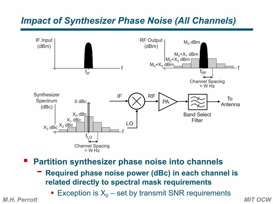
Impact of Synthesizer Phase Noise (All Channels)
Partition synthesizer phase noise into channels- Required phase noise power (dBc) in each channel is
related directly to spectral mask requirementsException is X0 – set by transmit SNR requirements
ffLO
SynthesizerSpectrum
(dBc)X0 dBc
0 dBc
X1 dBcX2 dBc
ffRF
RF Output(dBm)
M0 dBm
M0+X1 dBm
IF
LO
RF
fIFf
IF Input(dBm)
To Antenna
Band SelectFilter
PA
Channel Spacing= W Hz
Channel Spacing= W Hz
X3 dBc
M0+X3 dBmM0+X2 dBm
M.H. Perrott MIT OCW
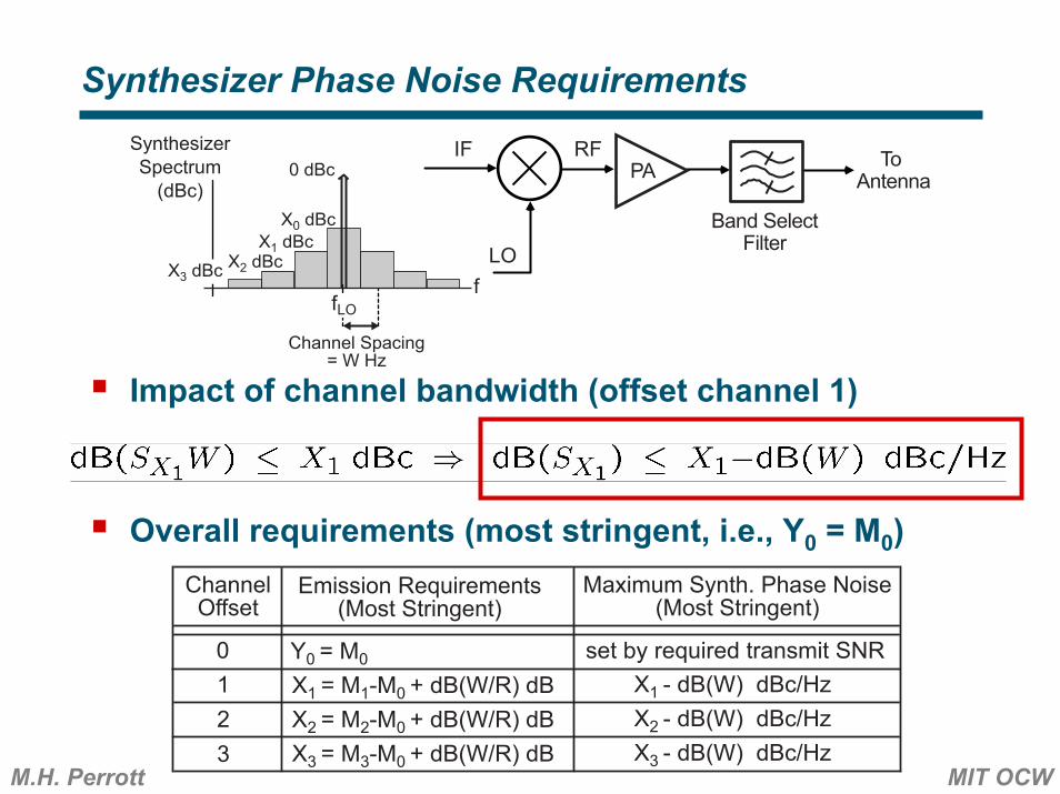
Synthesizer Phase Noise Requirements
Impact of channel bandwidth (offset channel 1)
Overall requirements (most stringent, i.e., Y0 = M0)
ffLO
SynthesizerSpectrum
(dBc)X0 dBc
0 dBc
X1 dBcX2 dBc
IF
LO
RF To Antenna
Band SelectFilter
PA
Channel Spacing= W Hz
X3 dBc
X1 - dB(W) dBc/HzX2 - dB(W) dBc/Hz
ChannelOffset
Maximum Synth. Phase Noise(Most Stringent)
12
X3 - dB(W) dBc/Hz3
X1 = M1-M0 + dB(W/R) dBX2 = M2-M0 + dB(W/R) dB
Emission Requirements(Most Stringent)
X3 = M3-M0 + dB(W/R) dB
0 Y0 = M0 set by required transmit SNR
M.H. Perrott MIT OCW
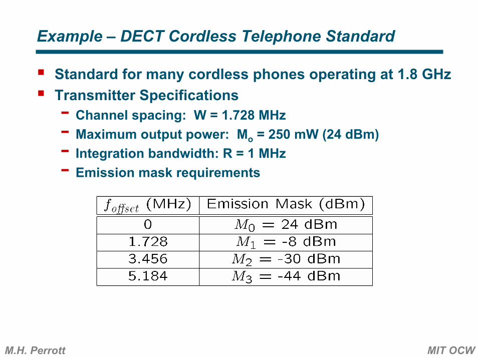
Example – DECT Cordless Telephone Standard
Standard for many cordless phones operating at 1.8 GHzTransmitter Specifications- Channel spacing: W = 1.728 MHz- Maximum output power: Mo = 250 mW (24 dBm)- Integration bandwidth: R = 1 MHz- Emission mask requirements

M.H. Perrott MIT OCW
Synthesizer Phase Noise Requirements for DECT
Using previous calculations with DECT values
Graphical display of phase noise mask
-8 dBm X1 = -29.6 dBcX2 = -51.6 dBc
-92 dBc/Hz-114 dBc/Hz
24 dBm
-30 dBm
ChannelOffset
MaskPower
Maximum Synth. NoisePower in Integration BW
Maximum Synth. Phase Noise at Channel Offset
01.728 MHz3.456 MHz
X3 = -65.6 dBc -128 dBc/Hz-44 dBm5.184 MHz
set by required transmit SNR
ffLO
SynthesizerSpectrum
(dBc)-92 dBc/Hz
-114 dBc/Hz
-128 dBc/Hz
Channel Spacing = 1.728 MHz

M.H. Perrott MIT OCW
Critical Specification for Phase Noise
Critical specification is defined to be the one that is hardest to meet with an assumed phase noise rolloff- Assume synthesizer phase noise rolls off at -20
dB/decadeCorresponds to VCO phase noise characteristic
For DECT transmitter synthesizer- Critical specification is -128 dBc/Hz at 5.184 MHz offset
ffLO
SynthesizerSpectrum
(dBc)-92 dBc/Hz
0 dBc
-114 dBc/Hz
-128 dBc/Hz
Channel Spacing = 1.728 MHz
Phase NoiseRolloff: -20 dB/dec
CriticalSpec.

M.H. Perrott MIT OCW
Receiver Blocking Performance
Radio receivers must operate in the presence of large interferers (called blockers)Channel filter plays critical role in removing blockers
Passes desired signal channel, rejects interferers
fRFf
Synthesizer
LNATo
IF ProcessingStage
Band SelectFilter
ChannelFilter
Band Select Filter MustPass All Channels
-73-58-39
RF Input(dBm)
fIF
fLO
f
Channel FilterBandwidth
IF Output(dBm)
f
SynthesizerSpectrum(dBc/Hz)
0 dBc

M.H. Perrott MIT OCW
Impact of Nonidealities on Blocking Performance
Blockers leak into desired band due to- Nonlinearity of LNA and mixer (IIP3)- Synthesizer phase and spurious noise
In-band interference cannot be removed by channel filter!
fRFf
Synthesizer
LNATo
IF ProcessingStage
Band SelectFilter
ChannelFilter
Band Select Filter MustPass All Channels
-73-58-39
RF Input(dBm)
fIF
fLO
f
Channel FilterBandwidth
IF Output(dBm)
Synthesizer Noise and Mixer/LNA Distortion
Produce Inband Interference
Phase Noise(dBc/Hz)
Spurious Noise(dBc)
f
SynthesizerSpectrum(dBc/Hz)
0 dBc

M.H. Perrott MIT OCW
Quantifying Tolerable In-Band Interference Levels
Digital radios quantify performance with bit error rate (BER)- Minimum BER often set at 1e-3 for many radio systems- There is a corresponding minimum SNR that must be achieved
Goal: design so that SNR with interferers is above SNRmin
fRFf
Synthesizer
LNATo
IF ProcessingStage
Band SelectFilter
ChannelFilter
Band Select Filter MustPass All Channels
-73-58-39
RF Input(dBm)
fIF
fLO
f
Channel FilterBandwidth
IF Output(dBm)
Synthesizer Noise and Mixer/LNA Distortion
Produce Inband Interference
Phase Noise(dBc/Hz)
Spurious Noise(dBc)
f
SynthesizerSpectrum(dBc/Hz)
Min SNR: 15-20 dB
0 dBc

M.H. Perrott MIT OCW
Impact of Synthesizer on Blockers
Synthesizer passes desired signal and blocker- Assume blocker is Y dB higher in signal power than
desired signal
fRFf
f
foffset
RF Input(dBm)
fIFf
fLO
IF Output(dBm)
SynthesizerSpectrum
(dBc) 0 dBc
Y dB
RF
LO
IF

M.H. Perrott MIT OCW
Impact of Synthesizer Spurious Noise on Blockers
Spurious tones cause the blocker (Y dB) (and desired) signals to “leak” into other frequency bands- In-band interference occurs when spurious tone offset
frequency is same as blocker offset frequency- Resulting SNR = -X-Y dB with spurious tone (X dBc)
fRFf
f
foffset
RF Input(dBm)
foffset
fIFf
fLO
IF Output(dBm)
SynthesizerSpectrum
(dBc)
X dBc
0 dBc
Y dB
SNR: -X-Y dBX dB
RF
LO
IF
SpuriousTone

M.H. Perrott MIT OCW
Impact of Synthesizer Phase Noise on Blockers
Same impact as spurious tone, but blocker signal is “smeared” by convolution with phase noise- For simplicity, ignore “smearing” and approximate as
shown above
fRFf
f
foffset
RF Input(dBm)
foffset
fIFf
fLO
IF Output(dBm)
SynthesizerSpectrum
(dBc)
X dBc
0 dBc
Y dB
SNR: -X-Y dBX dB
RF
LO
IF

M.H. Perrott MIT OCW
Blocking Performance Analysis (Part 1)
Ignore all out-of-band energy at the IF output- Assume that channel filter removes it- Motivation: simplifies analysis
fRFf
f
foffset
RF Input(dBm)
foffset
fIFf
fLO
SynthesizerSpectrum
(dBc)
X dBc
0 dBc
Y dB
SNR: -X-Y dB
RF
LO
IF
In-ChannelIF Output
(dBm)

M.H. Perrott MIT OCW
Blocking Performance Analysis (Part 2)
Consider the impact of blockers surrounding the desired signal with a given phase noise profile- SNRmin must be maintained- Evaluate impact on SNR one blocker at a time
ffLO
SynthesizerSpectrum
(dBc)
X0 dBc
0 dBc
X1 dBcX2 dBc
RF
LO
IF
fRFf
RF Input(dBm)
Y1 dBY2 dB
fIFf
Channel FilterBandwidth
In-ChannelIF Output
(dBm)
Inband InterferenceProduced by
Synth. Phase Noise
= W Hz
Channel Spacing
Channel Spacing
SNRmin: 15-20 dB

M.H. Perrott MIT OCW
Blocking Performance Analysis (Part 3)
ffLO
SynthesizerSpectrum
(dBc)
X0 dBc
0 dBc
X1 dBcX2 dBc
RF
LO
IF
fRFf
RF Input(dBm)
Y1 dBY2 dB
fIFf
Channel FilterBandwidth
In-ChannelIF Output
(dBm)
Inband InterferenceProduced by
Synth. Phase Noise
= W Hz
Channel Spacing
Channel Spacing
SNRmin: 15-20 dB
Y1 dB X1 = -SNRmin-Y1 dBcX2 = -SNRmin-Y2 dBcY2 dB
ChannelOffset
Relative BlockingPower
Maximum Synth. NoisePower at Channel Offset
12
X3 = -SNRmin-Y3 dBcY3 dB3
0 dB X0 = -SNRmin dBc0
Derive using the relationship
SNR = -X-Y dB >= SNRmin

M.H. Perrott MIT OCW
Blocking Performance Analysis (Part 4)
ffLO
SynthesizerSpectrum
(dBc)
X0 dBc
0 dBc
X1 dBcX2 dBc
RF
LO
IF
fRFf
RF Input(dBm)
Y1 dBY2 dB
fIFf
Channel FilterBandwidth
In-ChannelIF Output
(dBm)
Inband InterferenceProduced by
Synth. Phase Noise
= W Hz
Channel Spacing
Channel Spacing
SNRmin: 15-20 dB
Y1 dB X1 = -SNRmin-Y1 dBcX2 = -SNRmin-Y2 dBcY2 dB
ChannelOffset
Relative BlockingPower
Maximum Synth. NoisePower at Channel Offset
12
X3 = -SNRmin-Y3 dBcY3 dB3
0 dB X0 = -SNRmin dBc0X1 - dB(W) dBc/HzX2 - dB(W) dBc/Hz
Maximum Synth. PhaseNoise at Channel Offset
X3 - dB(W) dBc/Hz
X0 - dB(W) dBc/Hz
Convert power tospectral density

M.H. Perrott MIT OCW
Example – DECT Cordless Telephone Standard
Receiver blocking specifications- Channel spacing: W = 1.728 MHz- Power of desired signal for blocking test: -73 dBm- Minimum bit error rate (BER) with blockers: 1e-3
Sets the value of SNRmin
Perform receiver simulations to determine SNRmin
Assume SNRmin = 15 dB for calculations to follow- Strength of interferers for blocking test

M.H. Perrott MIT OCW
Synthesizer Phase Noise Requirements for DECT
ffLO
SynthesizerSpectrum
(dBc)
X0 dBc
0 dBc
X1 dBcX2 dBc
RF
LO
IF
fRFf
RF Input(dBm)
fIFf
Channel FilterBandwidth
In-ChannelIF Output
(dBm)
Inband InterferenceProduced by
Synth. Phase Noise
W = 1.73 MHz
Channel Spacing= 1.73 MHz
Channel Spacing= 1.73 MHz
SNRmin: 15 dB
Y1 = 15 dB X1 = -30 dBcX2 = -49 dBcY2 = 34 dB
ChannelOffset
Relative BlockingPower
Maximum Synth. NoisePower at Channel Offset
1.728 MHz3.456 MHz
X3 = -55 dBcY3 = 40 dB5.184 MHz
0 dB X0 = -15 dBc0-92 dBc/Hz
-111 dBc/Hz
Maximum Synth. PhaseNoise at Channel Offset
-117 dBc/Hz
-77 dBc/Hz
-73 dBm-58 dBm-39 dBm-33 dBm
X3 dBc

M.H. Perrott MIT OCW
Graphical Display of Required Phase Noise Performance
Mark phase noise requirements at each offset frequency
Calculate critical specification for receive synthesizer- Critical specification is -117 dBc/Hz at 5.184 MHz offset
Lower performance demanded of receiver synthesizer than transmitter synthesizer in DECT applications!
ffLO
SynthesizerSpectrum
(dBc)
-92 dBc/Hz
0 dBc
-111 dBc/Hz
-117 dBc/Hz
Channel Spacing = 1.728 MHz
Phase NoiseRolloff: -20 dB/dec
CriticalSpec.