689 ' # '5& *#6 & 7 - cdn.intechopen.comcdn.intechopen.com/pdfs-wm/40032.pdf · et al., 2005;...
23
3,350+ OPEN ACCESS BOOKS 108,000+ INTERNATIONAL AUTHORS AND EDITORS 114+ MILLION DOWNLOADS BOOKS DELIVERED TO 151 COUNTRIES AUTHORS AMONG TOP 1% MOST CITED SCIENTIST 12.2% AUTHORS AND EDITORS FROM TOP 500 UNIVERSITIES Selection of our books indexed in the Book Citation Index in Web of Science™ Core Collection (BKCI) Chapter from the book Nanoindentation in Materials Science Downloaded from: http://www.intechopen.com/books/nanoindentation-in-materials- science PUBLISHED BY World's largest Science, Technology & Medicine Open Access book publisher Interested in publishing with IntechOpen? Contact us at [email protected]
Transcript of 689 ' # '5& *#6 & 7 - cdn.intechopen.comcdn.intechopen.com/pdfs-wm/40032.pdf · et al., 2005;...

3,350+OPEN ACCESS BOOKS
108,000+INTERNATIONAL
AUTHORS AND EDITORS114+ MILLION
DOWNLOADS
BOOKSDELIVERED TO
151 COUNTRIES
AUTHORS AMONG
TOP 1%MOST CITED SCIENTIST
12.2%AUTHORS AND EDITORS
FROM TOP 500 UNIVERSITIES
Selection of our books indexed in theBook Citation Index in Web of Science™
Core Collection (BKCI)
Chapter from the book Nanoindentation in Materials ScienceDownloaded from: http://www.intechopen.com/books/nanoindentation-in-materials-science
PUBLISHED BY
World's largest Science,Technology & Medicine
Open Access book publisher
Interested in publishing with IntechOpen?Contact us at [email protected]

Chapter 12
© 2012 Zhao et al., licensee InTech. This is an open access chapter distributed under the terms of the Creative Commons Attribution License (http://creativecommons.org/licenses/by/3.0), which permits unrestricted use, distribution, and reproduction in any medium, provided the original work is properly cited.
Design, Analysis and Experiments of a Novel in situ SEM Indentation Device
Hongwei Zhao, Hu Huang, Zunqiang Fan, Zhaojun Yang and Zhichao Ma
Additional information is available at the end of the chapter
http://dx.doi.org/10.5772/48304
1. Introduction
Instrumented indentation as a powerful tool to determine mechanical properties of materials has been widely used in fields of materials science, biomechanics, surface engineering, semiconductor, MEMS/NEMS, biomedicine and so on (Fischer-Cripps, 2004) . Up to now, there are some commercially available indentation instruments. However, most of them can only carry out ex-situ indentation tests because of their complex structures and big volumes. In previous literatures, many phenomena such as pile-up and sink-in (Huang et al., 2005; Keryvin et al., 2010), which are difficult to explain but significantly affect the load-depth (P-h) curve and the determination of the contact area are observed. In order to reveal mechanical behavior of materials under the indentation load in detail and explain discontinuities during the initial loading segment better, more direct observation methods during indentation tests should be developed (Ghisleni et al., 2009).
In recent years, based on the transmission electron microscope (TEM) and scanning electron microscope (SEM), in situ indentation technique is presented by researchers (Gane & Bowden, 1968; Minor et al., 2001; Zhou et al., 2006). In situ TEM indentation has the capability to visually observe microstructure variations beneath the indenter such as phase transformation, dislocation formation and propagation (Minor et al., 2006), and dislocation-grain boundary interaction (De Hosson et al., 2006). But it also has disadvantages. For example, the specimens are very small and need complex and laborious preparation, and the specimens need to be electron transparent. In addition, the method that uses the mechanical properties of specimens with limited scale to evaluate the bulk materials is questionable (Ruffell et al., 2007). Via in situ SEM indentation, it is possible to observe the surface deformation during the whole indentation process, which is helpful to correct the reduced elastic modulus and hardness obtained by the Oliver and Pharr method (Oliver & Pharr, 2004) by accounting for pile-up and sink-in phenomena. In addition, mechanism of

Nanoindentation in Materials Science 288
deformation, crack formation and propagation, shear band formation, damage, pile-up, sink-in of materials will be studied deeply (Rzepiejewska-Malyska et al., 2009; Nowak et al., 2009). Compared with in situ TEM indentation, some physical phenomena such as phase transformation of materials, or nucleation and dislocation corresponding to high pressure applied by the indenter, are hardly observed by in situ SEM indentation. However, in situ SEM indentation is still a potential and attractive method because of its large field of view, simple specimen preparation and compatibility of materials with different dimensions from millimeter to micro/nanometer.
In this chapter, emphasis is put on in situ SEM indentation. Design of the indentation device compatible with the SEM has a few challenges (Huang et al., 2012), such as the small volume of the SEM chamber, short working distance, electromagnetic compatibility, the vacuum environment and vibration compatibility. Several studies of indentation inside the SEM have been done by researchers (Bangert et al., 1982; Bangert & Wagendristel, 1985; Motoki, 2006). The most representative are the device developed by Rabe in 2004 (Rabe et al., 2004) and the product — PI 85 SEM PicoIndenter manufactured by Hysitron Inc (Hysitron Incorporated). The load resolution of Rabe’s device is 100 μN for a range up to 1.5 N and the maximum available load is about 500 mN due to using the stick-slip actuator. Because of integrating a built-in strain gauge, the closed-loop displacement resolution is a little low about 50 nm with an indentation displacement range of 20 μm. The PI 85 SEM PicoIndenter has high load and displacement resolution about 3 nN and 0.02 nm respectively. However, the maximum indentation load is limited to be 10 mN and the maximum indentation displacement is 5 μm, which limits its more wide applications. In addition, this product is very expensive and up to now, there are very few scientists and researchers who can use this advanced equipment. So, in situ SEM indentation devices with large ranges, high precision, compact structures and low cost are still required.
In this chapter, a novel in situ indentation device with dimensions of 103 mm × 74 mm × 60 mm is developed and it is compatible with the SEM—Quanta 250. Integrating the stepper motor, the piezoelectric actuator and the flexure hinge, the coarse positioner and the precision driven unit were designed respectively, which can be used to realize coarse adjustment of the specimen and precision loading and unloading process of the indenter. A novel indenter holder was designed to ensure vertical penetration of the indenter. Closed-loop control of the indentation process was established to solve the problem of nonlinearity of the piezoelectric actuator and to enrich the control modes. Experiments were carried out to evaluate performances and verify the feasibility of the developed device.
2. Principle of in situ indentation tests inside the SEM
The schematic diagram of the developed indentation device for in situ indentation tests inside the SEM is shown in Fig. 1. Here, the diamond indenter is fixed and the specimen can move toward the indenter. This design considers the work distance of the SEM and makes the dimension of one side of the device small, which is helpful for in situ observation of the indentation region. The z axis coarse positioner driven by a stepper motor is designed to
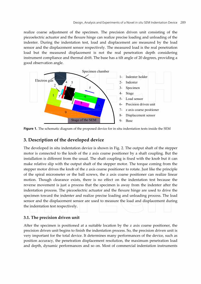
Design, Analysis and Experiments of a Novel in situ SEM Indentation Device 289
realize coarse adjustment of the specimen. The precision driven unit consisting of the piezoelectric actuator and the flexure hinge can realize precise loading and unloading of the indenter. During the indentation test, load and displacement are measured by the load sensor and the displacement sensor respectively. The measured load is the real penetration load but the measured displacement is not the real penetration depth considering instrument compliance and thermal drift. The base has a tilt angle of 20 degrees, providing a good observation angle.
1
2
3
4 5
6
78
9
Specimen chamber
Electron gun
Stage of the SEM
1- Indenter holder 2- Indenter 3- Specimen 4- Stage 5- Load sensor 6- Precision driven unit 7- z axis coarse positioner 8- Displacement sensor 9- Base
z
Figure 1. The schematic diagram of the proposed device for in situ indentation tests inside the SEM
3. Description of the developed device
The developed in situ indentation device is shown in Fig. 2. The output shaft of the stepper motor is connected to the knob of the z axis coarse positioner by a shaft coupling. But the installation is different from the usual. The shaft coupling is fixed with the knob but it can make relative slip with the output shaft of the stepper motor. The torque coming from the stepper motor drives the knob of the z axis coarse positioner to rotate. Just like the principle of the spiral micrometer or the ball screws, the z axis coarse positioner can realize linear motion. Though clearance exists, there is no effect on the indentation test because the reverse movement is just a process that the specimen is away from the indenter after the indentation process. The piezoelectric actuator and the flexure hinge are used to drive the specimen toward the indenter and realize precise loading and unloading process. The load sensor and the displacement sensor are used to measure the load and displacement during the indentation test respectively.
3.1. The precision driven unit
After the specimen is positioned at a suitable location by the z axis coarse positioner, the precision driven unit begins to finish the indentation process. So, the precision driven unit is very important for the total device. It determines many performances of the device, such as position accuracy, the penetration displacement resolution, the maximum penetration load and depth, dynamic performances and so on. Most of commercial indentation instruments

Nanoindentation in Materials Science 290
use electromagnetic and electrostatic drivers to realize precision motion of indenters. Due to complex structures and control of electromagnetic and electrostatic drivers, sizes of these indentation instruments are usually large. In addition, electromagnetic interference coming from these two kinds of drivers will affect the image of the SEM. So, they are not suitable for the design of in situ indentation devices.
Figure 2. Model of the developed in situ indentation device
Here, combining the piezoelectric actuator with the flexure hinge, a compact precision driven unit was designed as shown in Fig. 3. The piezoelectric actuator takes advantages of small size, unlimited resolution, large force generation, fast response, low power consumption and no wear (Huang et al., 2011; Huang et al., 2012). Also the flexure hinge can overcome shortcomings such as friction, lubrication and backlash which usually exist in the conventional mechanisms with sliding and rolling bearings (Kang et al., 2005). So, purpose of precision driving and miniaturization can be achieved easily by the combination of the piezoelectric actuator and the flexure hinge.
Figure 3. The precision driven unit

Design, Analysis and Experiments of a Novel in situ SEM Indentation Device 291
As shown in Fig. 3, the precision driven unit has a very simple structure which is helpful for the miniaturization of the device and can reduce the assembling. Also the simple structure is beneficial to the cleaning and it can reduce the import of pollution into the chamber of the SEM. The preload screw provides a preload force for the piezoelectric actuator to ensure suitable stiffness and displacement of the precision driven unit. The circular hinge was designed to reduce stress concentration of the flexure hinge. In order to ensure that the hinge has enough strength, structural static analysis of the flexure hinge was carried out by the software ANSYS 10.0. Material of spring steel 65Mn was selected to fabricate the hinge and its parameters are as follows. The Young's modulus is 206 GPa. The Poisson ratio is 0.288. As shown in Fig. 4(a), a displacement load of 10 μm was applied on the surface where the piezoelectric actuator was located. All degrees of freedom of the four installation holes were constrained. The analysis result is shown in Fig. 4(b). The maximum Von Mises stress is about 47.808 MPa which is less than the yield strength of 65Mn being 432 MPa. From the result, conclusion can be deduced that the flexure hinge is safety during the work process. In order to analyze the stress distribution of the hinge in depth, stress values of the hinge from point A to point B are extracted and drawn in Fig. 5. It is obvious that larger stress appears near the circular hinges. But the stress value is accepted.
Figure 4. Model and structural static analysis result of the flexure hinge. (a) shows the loading and boundary conditions in detail; (b) gives the maximum Von Mises stress under the analysis conditions
3.2. The indenter holder
During the indentation test, the indenter should penetrate into and withdraw from the surface of the specimen vertically, which should be guaranteed during the design. So, design of the indenter holder is important and an ingenious structure should be developed. In this paper, a novel indenter holder is proposed as shown in Fig. 6. Fig. 6 (a) is the assembly drawing of the indenter unit. Fig. 6 (b) is a local view of the indenter holder which was fabricated by wire-cutting. In the center of the indenter holder, a long and thin groove is designed. A hole located at the upper of the groove is used for installation of the indenter. The axis of the hole is parallel to the installation surface. The indenter uses the hole and the positioning surface to realize precision positioning and

Nanoindentation in Materials Science 292
then it is clamped by the lock nut. The positioning holes are designed to guarantee the position of the indenter holder and the installation holes are used to realize connection with the base.
Figure 5. Stress distribution of the flexure hinge from point A to point B
Figure 6. The designed indenter holder. (a) The assembly drawing of the indenter unit; (b) A local view of the indenter holder
4. Performance evaluation of the indentation device
The prototype of the developed in situ indentation device with dimensions of 103 mm × 74 mm × 60 mm was fabricated and assembled as shown in Fig. 7. Output performances of the device were tested.
4.1. Output performances of the z axis coarse positioner
The z axis coarse positioner is mainly used to realize coarse adjustment of the specimen and solve the problem that output displacement of the piezoelectric actuator is very limited. So, larger range with certain accuracy is required for the z axis coarse positioner. Output performances of the z axis coarse positioner were tested with the established test system as
02468
10121416
0 10 20 30 40Distance from point A /mm
Stre
ss /M
Pa

Design, Analysis and Experiments of a Novel in situ SEM Indentation Device 293
shown in Fig. 8. The stepper motor drives the stage to output displacement which is measured by the laser displacement sensor with the resolution of 10 nm. The measured signal is collected and sent to the computer for further processing. Define the parameter n as pulses per step and it can be given different value for the stepper motor. Fig. 9 is the output displacement curves when n=2048, 100 and 10 respectively. Obvious difference is observed. When n=2048, large and continuous output displacement about 239 μm/step is obtained, which can be used for coarse adjustment of the specimen when it is far away from the indenter. When n=100 and 10, small output displacement per step, about 10 μm/step for n=100 and 0.333 μm/step for n=10, is obtained. The case that n is given a small value can be used when the specimen is near the indenter. Analyzing the experimental results, we can get another difference. That is, for different n, the average output displacement per pulse is different. Maybe this is caused by the crawl phenomenon between the guide rail and the slider of the z axis coarse positioner. This difference has no effect on the indentation process because the z axis coarse positioner is only used for coarse adjustment rather than precision loading and unloading.
Figure 7. The prototype of the developed in situ indentation device
Figure 8. The established system for output performance tests of the z axis coarse positioner

Nanoindentation in Materials Science 294
4.2. Output performances of the precision driven unit with open-loop control
Output performances of the precision driven unit with open-loop control were tested. Use the power to supply voltage signal to the piezoelectric actuator manually and the output displacement is measured by the embedded displacement sensor. The experimental results are shown in Fig. 10 and Fig. 11. Fig. 10 indicates that the manual displacement resolution is about 20 nm. Fig. 11 gives the maximum output displacement of the precision driven unit about 11.44 μm when the maximum applied voltage is 100 V. With open-loop control, the precision driven unit has certain accuracy. But nonlinearity mainly caused by hysteresis of the piezoelectric actuator is also existed as shown in Fig. 11, which will affect the indentation process. So, measures should be taken to ensure linear output of the precision driven unit.
050
100150200250300
0 200 400 600 800Sampling points
Dis
plac
emen
t /μm
0
50
100
150
200
0 500 1000 1500 2000Sampling points
Dis
plac
emen
t /μm
0
1
2
3
4
5
0 300 600 900 1200 1500Sampling points
Dis
plac
emen
t /μm
Figure 9. Output displacement curves of the z axis coarse positioner with different n. (a) n=2048; (b) n=100; (c) n=10

Design, Analysis and Experiments of a Novel in situ SEM Indentation Device 295
Figure 10. Resolution plot of the precision driven unit with manual operation
Figure 11. The output displacement curve of the precision driven unit with the maximum applied voltage of 100 V
4.3. Closed-loop control of the indentation process
In order to solve the problem of nonlinearity and ensure the testing stability, closed-loop control of the indentation process is established. Fig. 12 is the control schematic. Two control modes are developed, the displacement control mode and the load control mode. Here takes the displacement control mode as an example. Control parameters such as the maximum output displacement and the loading time, are set by the software. Control orders are sent to the power via parallel communication. The power applies voltage signal to the piezoelectric actuator and then the actuator outputs precise displacement which is measured by the embedded displacement sensor. The measured displacement signal is collected by the A/D card and sent to the PC. Comparing the measured value with the setting value, error value is obtained and then sent to the power. Repeat the process above until the measured value is equal to the setting value.
Under ambient temperature and general testing circumstance without constant temperature control and vibration isolation, three different maximum displacements and three different loads are selected to verify the feasibility of closed-loop control. Typical displacement
00.010.020.030.040.050.060.07
0 200 400 600 800Sampling points
Dis
plac
emen
t /μm
02468
1012
0 5000 10000Sampling points
Dis
plac
emen
t /μm 11.45μm

Nanoindentation in Materials Science 296
control results and load control results are shown in Fig. 13 and Fig. 14 respectively. Via closed-loop control, output is continues and linear. Obviously, when the output displacement and load are small, fluctuations appear. In order to quantify fluctuations, a constant output displacement of 2 μm and a constant load of 20 mN were kept for 100 second respectively under the above testing circumstance. The fluctuation curves are shown in Fig. 15. Amplitude of the displacement fluctuation is less than 20 nm and amplitude of the load fluctuation is about 140 μN without constant temperature control and vibration isolation. Compared with open-loop control, closed-loop control can ensure good linearity output. Also, abundant loading and unloading modes can be developed via closed-loop control.
Figure 12. Closed-loop control schematic of the indentation process
0 20 40 600
0.02
0.04
0.060.05
0.0550.045
0.01
0.03
0 10 20 30 40 50 60600
0.10.20.30.40.50.60.6
0 10 20 30 40 50 606002468
101212
Figure 13. Typical displacement control results
4.4. Repeatability of the developed device
Comparing the load-displacement curves for different maximum loads is a good method to evaluate the repeatability of the indentation instrument. Fig. 16 shows curves between the load and the measured displacement resulting from 10 ex-situ indentation tests on fused quartz under ambient temperature and general testing circumstance without constant temperature control and vibration isolation. The loading curves agree well with each other and the unloading curves distinguish with each other because of different maximum indentation loads. The results indicate that the developed device has good repeatability, which is the premise for further calibration.

Design, Analysis and Experiments of a Novel in situ SEM Indentation Device 297
0 10 20 30 40 50 606001234566
0 10 20 30 40 50 60600
10203040506060
0 10 20 30 40 50 600
20406080
100120120
Figure 14. Typical load control results
0 20 40 60 80 1001.99
1.995
2
2.005
2.01
Dis
plac
emen
t /μm
0 20 40 60 80 100
20
20.05
20.1
20.15
19.96
Load
/mN
Figure 15. Output results for a constant output displacement of 2 μm (a) and a constant load of 20 mN (b)
4.5. Thermal drift
Two kinds of drift behaviors, creep within the specimen as a result of plastic flow and thermal drift due to thermal expansion or contraction of the apparatus are observed in indentation tests. Creep is time-dependent deformation under the constant load or stress and it is related with viscoelastic or viscoplastic deformation of materials. Thermal drift comes from the instrument itself and the circumstance, and it will cause the measured displacement ht larger or smaller than the actual indentation depth h. So measures should be taken to correct the thermal drift. Assuming that the thermal drift for an indentation test is constant, the developed device allows for a hold series of data points to be accumulated at the end of the unloading from the maximum load. During the hold period at the end of the unloading, creep is less likely to occur because the load is very low. Then fitting the load and measured displacement, the thermal drift rate will be obtained. As shown in Fig. 17, thermal drift rate for the indentation test of fused quartz is about -0.5 nm/s. The corrected and uncorrected curves are shown in Fig. 18.

Nanoindentation in Materials Science 298
Load
P/m
N
Figure 16. Curves between the load and the measured displacement resulting from 10 ex-situ indentation tests on fused quartz
4.6. Determination of instrument compliance Cm
Instrument compliance Cm is the most important factor that affects the load-depth curve, which also makes the measured displacement ht larger than the actual indentation depth h. Especially, when the instruments are miniaturization, this effect will be even more obvious, making calibration of instrument compliance more difficult. Commercial ex-situ indentation instruments exhibit Cm in the range of 0.1 nm/mN to 1 nm/mN. But in situ indentation devices developed by previous researchers obviously have larger compliance because of their miniaturization structures. Instrument compliance of Rabe’s device is about 5 nm/mN while instrument compliance of the PicoIndenter is not determined in literature (Rzepiejewska-Malyska et al., 2008; Ghisleni et al., 2009). Although in situ indentation pays more attention to visually and dynamically observe the deformation and damage process of materials (Rzepiejewska-Malyska et al., 2008) and properties of materials can be obtained by the ex-situ indentation tests, accurate and quantitative load-depth curves are also required which are helpful to make the connection between the surface deformation and the applied indentation load.
Considering instrument compliance Cm, relationship between the actual indentation depth h and the measured displacement ht can be given as (Oliver & Pharr, 1992)
h = ht -CmP (1)
where P is the indentation load.
There are a few methods proposed by previous researchers to calibrate instrument compliance (Doerner & Nix, 1986; Van Vliet et al., 2004; Nurot & Sun, 2005), and the most representative method is the iterative procedure developed by Oliver and Pharr (Oliver & Pharr, 2004) based on the assumption that Young’s modulus of the sample does not vary

Design, Analysis and Experiments of a Novel in situ SEM Indentation Device 299
with indentation depth, but their method is mathematically and time intensive (Costa et al., 2004). Here, like the literature (Huang et al., 2011), a reference material Indium-Tin Oxide (ITO) and a commercial indentation instrument-CSM’s Nanoindentation Tester are used to calibrate instrument compliance of the developed device.
0.37
0.38
0.39
0.4
0.41
0.42
0.43
0.44
0.45
0 50 100 150 200
Figure 17. Relationship between the measured displacement ht and time for a constant load
0
10
20
30
40
50
60
70
80
0 0.3 0.6 0.9 1.2Measured displacement ht/μm
Load
P/m
N
+○
CorrectedUncorrected
Corrected
Uncorrected
Figure 18. Comparison of the uncorrected curve and the corrected curve considering of the thermal drift
Indentation tests of ITO with maximum indentation loads of 30 mN, 50 mN, 100 mN, 150 mN, 250 mN and 500 mN were carried out with the Berkovich indenter using the CSM’s Nanoindentation Tester and the experimental curves are used as standard load-depth curves. Then, with the same experimental conditions, indentation tests were carried out using the developed in situ SEM indentation device. By comparing curves obtained from the commercial device and the designed device, six values of instrument compliance can be

Nanoindentation in Materials Science 300
obtained respectively, and the average value of 4.5 nm/mN is obtained as instrument compliance Cm, which is also larger than values of commercial ex-situ indentation instruments. By equation (1), the corrected curve with the maximum indentation load of 500 mN can be obtained as shown in Fig. 19. The slope of the corrected curve is obviously larger than that of the raw curve while the unloading point remains the same because the load is zero. In order to verify the feasibility of the calibration result, the corrected curve and the curve obtained from the commercial device are drawn in the same figure shown in Fig. 20, from which we can see that these two curves coincide with each other well. According to the Oliver and Pharr method (Oliver & Pharr, 1992), the contact depth between the indenter and the sample is about 1.709 μm and hardness of ITO is about 6.97 GPa. Indentation tests of single crystal copper and bulk metallic glass in the following section will verify generality of instrument compliance.
0 1 2 3 4 50
100
200
300
400
500
600
Depth h/μm
Load
P/m
N
Raw curve
Corrected curve CmP
Figure 19. The corrected curve and the raw curve
0 0.5 1 1.5 2 2.5 30
100
200
300
400
500
600
Load
P/m
N
Figure 20. Comparison between curves from the commercial device and the designed device

Design, Analysis and Experiments of a Novel in situ SEM Indentation Device 301
4.7. Parameter comparison with the existing product or device
Up to now, work related with in situ indentation is concentrated on Rabe’s device (Rabe et al., 2004), the PI 85 SEM PicoIndenter (Hysitron Incorporated) and the self-made device (Huang et al., 2012). Here, main parameters of these three devices are summarized in Table 1. Comparing these parameters, the self-made in situ indentation device has the advantage in high price-performance ratio.
Self-made device
Rabe’s device
PI 85 SEM PicoIndenter
Maximum load 2.5 N 500 mN 10 mN
Maximum displacement 15 μm 20 μm 5 μm
Load noise floor 140 μN Unknown 400 nN
Displacement noise floor 20 nm Unknown 1 nm
Load resolution 50 μN 100 μN 3 nN
Displacement resolution 5 nm 50 nm 0.02 nm
Compliance 4.5 nm/mN 5 nm/mN Unknown
x positioning range 12 μm (Addible) 10 mm 5 mm
x positioning resolution 10 nm 150 nm 50 nm
y positioning range 12 μm (Addible) 20 μm 5 mm
y positioning resolution 10 nm 7 nm 50 nm
Price (include tax) $100, 000.00 $100, 000.00 $ 250, 000.00
Table 1. Summarized parameters of three kinds of main in situ indentation devices
5. Indentation tests
5.1. Ex-situ indentation tests
The developed indentation device has the miniaturized structure but still it has the function to carry out ex-situ indentation tests. Fig. 21 is the load-depth curve of single crystal copper via the ex-situ indentation test under ambient temperature and general testing circumstance without constant temperature control and vibration isolation. Fig. 22 is the fitting curve of the unloading portion.
According to the literature (Oliver & Pharr, 1992), the unloading curves are distinctly curved and usually well approximated by the power law relation:
f( )mP h hα= − (2)

Nanoindentation in Materials Science 302
where α and m are power law fitting constants, and hf is the depth of the residual impression. By fitting portion of the unloading data with the least squares fitting procedure, the constants α and m can be obtained. The fitting results are given in Fig. 22 and the fitting equation is expressed as
1.2450804.709( 0.757)P h= − (3)
According to the Oliver and Pharr method (Oliver & Pharr, 1992), hardness of single crystal copper is 0.95 GPa and the Young's modulus is 107.42 GPa.
0 0.2 0.4 0.6 0.8 10
3
6
9
12
15
1818
Load
P/m
N
Figure 21. The load-depth curve of single crystal copper
5.2. In situ indentation test inside the SEM
Due to unique mechanical properties such as high strength, modulus, hardness and elastic limit (Inoue et al., 2004; Scully et al., 2007), bulk metallic glasses (BMGs) are considered as emerging structural materials since their discovery in 1960 (Klement et al., 1960). Mechanical properties and deformation mechanism of BMGs are given more and more attention in recent years. Because of its high spatial and temporal resolution, indentation remains an important tool to study mechanical properties of BMGs (Schuh, 2006). Unique phenomena such as the serrated flow and shear band formation underneath indenters have been reported during the ex-situ indentation tests (Wang et al., 2000; Schuh & Nieh, 2003; Li et al., 2009). However, most of previous researchers can only study shear band formation of BMGs after the indentation tests, limiting further research on the deformation mechanism. Here, in situ indentation of a Zr-based bulk metallic glass using the Berkovich indenter was carried out via the developed device.

Design, Analysis and Experiments of a Novel in situ SEM Indentation Device 303
The device was installed on the stage of the SEM—Quanta 250. The experimental results are shown in Fig. 23. The load-depth curve is shown in Fig. 23 (a). Fig. 23 (b) is the status that there is a distance between the indenter and the specimen. Fig. 23 (c) is the status that the indenter is penetrating into the specimen. Fig. 23 (d) is the indentation morphology. From Fig. 23 (c) and (d), pile-up and shear bands are observed obviously. This is only an example of in situ indentation tests inside the SEM. Via in situ observation of a whole indentation process, more direct inspection of deformation and damage of materials can be realized, bringing the possibility of further studying and revealing deformation and damage mechanism of materials.
0.65 0.7 0.75 0.8 0.852
4
6
8
10
12
14
16
Figure 22. The fitting results of portion of the unloading data
Of course, in situ indentation techniques can be used for other research. Taking advantage of high positioning accuracy, it can be used to study effect of initial contact and surface roughness on experimental results. Using a special indenter such as the flat-ended indenter, in situ uniaxial compression of micro- and nano- structures for example carbon nanotubes and micropillars can be carried out (Buzzi et al., 2009; Niederberger et al., 2010). Also, using a suitable clamping way, in situ tensile tests are feasible (Lucca et al., 2010). Adding heating or precise electrical measuring equipments, the device can be used to study multi-physical field coupled performance of materials (Schuh et al., 2005; Nowak et al., 2009) which will be an exciting and significant work. So, the in situ indentation test inside the SEM is a promising method to study mechanics of materials in depth.

Nanoindentation in Materials Science 304
Figure 23. Experimental results of the in situ indentation test of a Zr-based bulk metallic glass. Fig. 23 (a) is the load-depth curve. Fig. 23 (b) is the status that there is a distance between the indenter and the specimen. Fig. 23 (c) is the status that the indenter is penetrating into the specimen. Fig. 23 (d) is the indentation morphology
6. Conclusions
In this chapter, a novel and miniaturization in situ indentation device was presented. Integrating the stepper motor, the piezoelectric actuator and the flexure hinge, the coarse positioner and the precision driven unit were designed respectively, which can be used to realize coarse adjustment of the specimen and precision loading and unloading process of the indenter. A novel indenter holder was designed to ensure vertical penetration of the indenter. Closed-loop control of the indentation process was established to solve the problem of nonlinearity of the piezoelectric actuator and to enrich the control modes.
Performances of the developed device were evaluated, and ex-indentation and in situ indentation tests of materials were carried out to verify the feasibility of the device. The device has the indentation load range of about 2.5 N with the load resolution of 50 μN and indentation depth range of about 15 μm with the displacement resolution of 5 nm. Compliance of the device was calibrated and it is about 4.5 nm/mN. Also thermal drift was corrected. Experimental results indicate that the developed device has good repeatability and it can be used as an ex-situ indentation device to characterize properties of materials. What’s more, it can be installed on the stage of the SEM to realize

Design, Analysis and Experiments of a Novel in situ SEM Indentation Device 305
in situ indentation tests of materials, which is a promising method to study deformation and damage mechanism of materials in depth. Compared with other two in situ indentation device or product, the developed in situ indentation device has the advantage in high price-performance ratio. By in situ indentation tests and other extended applications, it is hoped that the developed device will be a significant tool for advanced materials research.
Author details
Hongwei Zhao, Hu Huang, Zunqiang Fan, Zhaojun Yang and Zhichao Ma Jilin University, China
Acknowledgement
This research is funded by the National Natural Science Foundation of China (Grant No. 50905073, 51105163), National Hi-tech Research and Development Program of China(863 Program) (863 Program) (Grant No. 2012AA041206), Key Projects of Science and Technology Development Plan of Jilin Province (Grant No. 20110307) and International Science and Technology Cooperation Program of China (Grant No. 2010DFA72000). We also gratefully acknowledge Institute of Microstructure and Properties of Advanced Materials, Beijing University of Technology for the support of the SEM.
7. References
Bangert, H., Wagendristel, A. & Aschinger, H. (1982). Ultramicrohardness measurement on thin films, fibers and finely structured surfaces. Vacuum. Tech., Vol.31, pp. 200–203
Bangert, H. & Wagendristel, A. (1985). Ultralow-load hardness tester for use in a scanning electron microscope. Rev. Sci. Instrum., Vol.56, pp. 1568-1572
Buzzi, S., Dietiker, M., Kunze, K., Spolenak, R. & Löffler, J.F. (2009) Deformation behavior of silver submicrometer-pillars prepared by nanoimprinting. Philos. Mag., Vol.89, pp. 869-884
Costa, A.L.M., Shuman, D.J., Machado, R.R. & Andrade, M.S. (2004). Determination of the Compliance of an Instrumented Indentation Testing Machine, In: Proc. of HARDMEKO, Washington D.C., USA
De Hosson, J.T.M., Soer, W.A., Minor, A.M., Shan, Z., Stach, E.A., Asif, S.A. & Warren, O.L. (2006). In situ TEM nanoindentation and dislocation-grain boundary interactions: a tribute to David Brandon. J. Mech. Sci., Vol.41, pp. 7704-7719
Doerner, M.F. & Nix, W.D. (1986). A method for interpreting the data from depth-sensing indentation instruments. J. Mater. Res., Vol.1, pp.601-609
Fischer-Cripps, A.C. (2004). Nanoindentation. Springer-Verlag, New York Gane, N. & Bowden, F.P. (1968). Microdeformation of Solids. J. Appl. Phys., Vol.39, pp. 1432-
1435

Nanoindentation in Materials Science 306
Ghisleni, R., Rzepiejewska-Malyska, K., Philippe, L., Schwaller, P. & Michler, J. (2009). In situ SEM indentation experiments: Instruments, methodology, and applications. Microsc. Res. Techniq., Vol.72, pp. 242-249
Huang, W.M., Su, J.F., Hong, M.H. & Yang, B. (2005). Pile-up and sink-in in micro-indentation of a NiTi shape-memory alloy. Scripta Mater., Vol.53, pp. 1055–1057
Huang, H., Zhao, H., Yang, J., Wan, S., Mi, J., Shi, C., Yuan, Y., Ma, Z. & Yang, Z. (2011). Design and analysis of a miniaturization nanoindentation and scratch device. Advanced Materials Research, Vol.314-316, pp. 1792-1795
Huang, H., Zhao, H., Mi, J., Yang, J., Wan, S., Yang, Z., Yan, J., Ma, Z. & Geng, C. (2011). Experimental research on a modular miniaturization nanoindentation device. Rev. Sci. Instrum., Vol.82, pp. 095101 (1-6)
Huang, H., Zhao, H., Ma, Z., Hu, L., Yang, J., Shi, G., Ni, C., Pei, Z. (2012) Design and analysis of the precision-driven unit for nano-indentation and scratch test. J. Manuf. Syst., Vol.31, pp. 76–81
Huang, H., Zhao, H., Mi, J., Yang, J., Wan, S., Xu, L. & Ma, Z. (2012). A novel and compact nanoindentation device for in situ nanoindentation tests inside the scanning electron microscope. AIP Advances, Vol.2, 012104 (1-10)
Hysitron Incorporated. Cited 2011; Available from: http://www.hysitron.com/ Inoue, A., Shen, B.L., Koshiba, H., Kato, H. & Yavari, A.R. (2004). Ultra-high strength above
5000 MPa and soft magnetic properties of Co–Fe–Ta–B bulk glassy alloys. Acta Mater., Vol.52, pp. 1631–1637
Kang, D., Kim, K., Choi, Y., Gweon, D., Lee, S. & Lee, M. (2005). Design and control of flexure based XYθz stage. J. Mech. Sci. Technol., Vol.19, pp. 2157-2164
Keryvin, V., Vu, X.D., Hoang, V.H. & Shen, J. (2010). On the deformation morphology of bulk metallic glasses underneath a Vickers indentation. J. Alloys Compd., Vol.504S, pp. S41-S44
Klement, W., Wilens, R.H. & Duwez, P. (1960). Non-crystalline Structure in Solidified Gold–Silicon Alloys. Nature, Vol.187, pp. 869-870
Li, N., Liu, L., Chan, K.C., Chen, Q. & Pan, J. (2009). Deformation behavior and indentation size effect of Au49Ag5.5Pd2.3Cu26.9Si16.3 bulk metallic glass at elevated temperature. Intermetallics, Vol.17, pp. 227-230
Lucca, D.A., Herrmann, K. & Klopfstein, M.J. (2010). Nanoindentation: Measuring methods and applications. CIRP Ann.-Manuf. Techn., Vol.59, pp. 803-819
Minor, A.M., Morris, J.W. & Stach, E.A. (2001). Quantitative in situ nanoindentation in an electron microscope. Appl. Phys. Lett., Vol.79, pp. 1625-1627
Minor, A.M., Asif, S.A., Shan, Z., Stach, E.A., Cyrankowski, E., Wyrobek, T.J. & Warren, O.L. (2006). A new view of the onset of plasticity during the nanoindentation of aluminum. Nat. Mater., Vol.5, pp. 697-702
Motoki, T., Gao, W., Kiyono, S. & Ono, T. (2006). A nanoindentation instrument for mechanical property measurement of 3D micro/nano-structured surfaces. Meas. Sci. Technol. Vol.17, pp. 495-499

Design, Analysis and Experiments of a Novel in situ SEM Indentation Device 307
Niederberger, C., Mook, W.M., Maeder, X. & Michler, J. (2010). In situ electron backscatter diffraction (EBSD) during the compression of micropillars. Mater. Sci. Eng. A, Vol.527, pp. 4306–4311
Nowak, R., Chrobak, D., Nagao, S., Vodnick, D., Berg, M., Tukiainen, A. & Pessa, M. (2009). An electric current spike linked to nanoscale plasticity. Nat. Nanotechnol., Vol.4, pp. 287-291
Nowak, J.D., Rzepiejewska-Malyska, K., Major, R.C., Warren, O.L. & Michler, J. (2009) In-situ nanoindentation in the SEM. Mater. Today, Vol.12, pp. 44-45
Nurot, P. & Sun, Y. (2005). Improved method to determine the hardness and elastic moduli using nano-indentation. KMITL Sci. J., Vol.5, pp. 483-492
Oliver, W.C. & Pharr, G.M. (2004). Measurement of hardness and elastic modulus by instrumented indentation: Advances in understanding and refinements to methodology. J. Mater. Res., Vol.19, pp. 3–20
Oliver, W.C. & Pharr, G.M. (1992). An improved technique for determining hardness and elastic modulus using load and displacement sensing indentation measurements. J. Mater. Res., Vol.7, pp.1564-1583
Rabe, R., Breguet, J.-M., Schwaller, P., Stauss, S., Haug, F.-J., Patscheider, J. & Michler J. (2004). Observation of fracture and plastic deformation during indentation and scratching inside the scanning electron microscope. Thin Solid Films, Vol.469/470, pp. 206–213
Ruffell, S., Bradby, J.E., Williams, J.S. & Munroe, P. (2007). Formation and growth of nanoindentation-induced high pressure phases in crystalline and amorphous silicon. J. Appl. Phys., Vol.102, pp. 063521 (1-8)
Rzepiejewska-Malyska, K., Buerki, G., Michler, J., Major, R.C., Cyrankowski, E., Asif, S.A.S. & Warren O.L. (2008). In situ mechanical observations during nanoindentation inside a high-resolution scanning electron microscope. J. Mater. Res., Vol.23, pp. 1973-1979
Rzepiejewska-Malyska, K., Parlinska-Wojtan, M., Wasmer, K., Hejduk, K. & Michler, J. (2009). In-situ SEM indentation studies of the deformation mechanisms in TiN, CrN and TiN/CrN. Micron, Vol.40, pp. 22-27
Schuh, C.A. & Nieh, T.G. (2003). A nanoindentation study of serrated flow in bulk metallic glasses. Acta Mater., Vol.51, pp. 87-99
Schuh, C.A., Mason, J.K. & Lund, A.C. (2005). Quantitative insight into dislocation nucleation from high-temperature nanoindentation experiments. Nat. Mater., Vol.4, pp. 617-621
Schuh, C.A. (2006). Nanoindentation studies of materials. Mater. Today, Vol.9, pp. 32-40 Scully, J.R., Gebert, A. & Payer, J.H. (2007). Corrosion and related mechanical properties of
bulk metallic glasses. J. Mater. Res., Vol.22, pp. 302-313 Van Vliet, K.J., Prchlik, L. & Smith, J.F. (2004). Direct measurement of indentation frame
compliance. J. Mater. Res., Vol.19, pp. 325-331

Nanoindentation in Materials Science 308
Wang, J.G., Choi, B.W., Nieh, T.G. & Liu, C.T. (2000). Crystallization and nanoindentation behavior of a bulk Zr–Al–Ti–Cu–Ni amorphous alloy. J. Mater. Res., Vol.15, pp. 798-807
Zhou, J., Komvopoulos, K. & Minor, A.M. (2006). Nanoscale plastic deformation and fracture of polymers studied by in situ nanoindentation in a transmission electron microscope. Appl. Phys. Lett., Vol.88, pp. 181908 (1-3)


![79: ' # '6& *#7 & 8 - cdn.intechopen.comcdn.intechopen.com/pdfs-wm/46244.pdf · &kdswhu 'hyhorsphqwvlq5holdelolw\ %dvhg$vvhvvphqwri &ruurvlrq =dkludql]d0xvwdiid $gglwlrqdolqirupdwlrqlvdydlodeohdwwkhhqgriwkhfkdswhu](https://static.fdocuments.in/doc/165x107/5a73e6637f8b9a93088b6a98/79-6-7-8-cdn-kdswhu-hyhorsphqwvlq5holdelolw-dvhgvvhvvphqwri.jpg)
![Temperature dependence of mechanical properties and …materials.iisc.ernet.in/~ramu/publications/paper77.pdf · 1774 V. Keryvin et al. XML Template (2008) [23.8.2008–4:43pm] [1773–1790]](https://static.fdocuments.in/doc/165x107/5b9b444c09d3f21b2f8cec18/temperature-dependence-of-mechanical-properties-and-ramupublicationspaper77pdf.jpg)