60MSPS 3-Channel AFE with Multiple Device Operation and ... · w WM8224 60MSPS 3-Channel AFE with...
50
w WM8224 60MSPS 3-Channel AFE with Multiple Device Operation and Programmable Automatic Black Level Calibration WOLFSON MICROELECTRONICS plc Production Data, September 2013, Rev 4.2 Copyright 2013 Wolfson Microelectronics plc. DESCRIPTION The WM8224 is an analogue front end/digitiser IC which processes and digitises the analogue output signals from CCD sensors or Contact Image Sensors (CIS) at pixel sample rates of up to 60MSPS. The device includes three analogue signal processing channels each of which contains Reset Level Clamping, Correlated Double Sampling and Programmable Gain and Offset adjust functions. The output from each of these channels is time multiplexed into a single high-speed 16-bit Analogue to Digital Converter. The digital data is available in a variety of output formats via the flexible data port. An internal 4-bit DAC is supplied for internal reference level generation. This may be used during CDS to reference CIS signals or during Clamping to clamp CCD signals. An external reference level may also be supplied. ADC references are generated internally, ensuring optimum performance from the device. A programmable automatic Black-Level Calibration function is available to adjust the DC offset of the output data. A daisy chain feature allows multiple devices to operate together using the same control interface and output data bus. FEATURES 12 or 16-bit ADC, 40MSPS conversion rate 8 or 10-bit ADC, 60MSPS conversion rate Low power – 360 mW typical 3.3V single supply operation 3 channel operation Daisy Chain feature for multiple device use Correlated double sampling Programmable gain (9-bit resolution) Programmable offset adjust (8-bit resolution) Flexible clamp timing Programmable clamp voltage Internally generated voltage references Automatic Black Level Calibration 32-lead QFN package Serial control interface APPLICATIONS Digital Copiers USB2.0 compatible scanners Multi-function peripherals High-speed CCD/CIS sensor interface BLOCK DIAGRAM RINP DATA O/P PORT SEN VSMP MCLK VRLC/VBIAS SDI SCK TIMING CONTROL CLMP RLC V S R S BINP GINP VRX VRT OEB VRB RLC RLC CDS CDS CDS RLC DAC 16- BIT ADC AGND1 DGND DVDD OP[2] OP[3] OP[4] OP[5] OP[6] OP[7] OP[8] AGND2 M U X VREF/BIAS + PGA I/P SIGNAL POLARITY ADJUST PGA OFFSET DAC PGA OFFSET DAC + + + + + I/P SIGNAL POLARITY ADJUST I/P SIGNAL POLARITY ADJUST AVDD WM8224 RSMP OP[9] OFFSET DAC OP[0] OP[1] DSLCT SERIAL CONTROL INTERFACE BLACK LEVEL CALIBRATION + OP[11]/SDO OP[10]
Transcript of 60MSPS 3-Channel AFE with Multiple Device Operation and ... · w WM8224 60MSPS 3-Channel AFE with...

w WM8224
60MSPS 3-Channel AFE with Multiple Device Operation
and Programmable Automatic Black Level Calibration
WOLFSON MICROELECTRONICS plc
Production Data, September 2013, Rev 4.2
Copyright 2013 Wolfson Microelectronics plc.
DESCRIPTION
The WM8224 is an analogue front end/digitiser IC which processes and digitises the analogue output signals from CCD sensors or Contact Image Sensors (CIS) at pixel sample rates of up to 60MSPS.
The device includes three analogue signal processing channels each of which contains Reset Level Clamping, Correlated Double Sampling and Programmable Gain and Offset adjust functions. The output from each of these channels is time multiplexed into a single high-speed 16-bit Analogue to Digital Converter. The digital data is available in a variety of output formats via the flexible data port.
An internal 4-bit DAC is supplied for internal reference level generation. This may be used during CDS to reference CIS signals or during Clamping to clamp CCD signals. An external reference level may also be supplied. ADC references are generated internally, ensuring optimum performance from the device.
A programmable automatic Black-Level Calibration function is available to adjust the DC offset of the output data. A daisy chain feature allows multiple devices to operate together using the same control interface and output data bus.
FEATURES 12 or 16-bit ADC, 40MSPS conversion rate
8 or 10-bit ADC, 60MSPS conversion rate
Low power – 360 mW typical
3.3V single supply operation
3 channel operation
Daisy Chain feature for multiple device use
Correlated double sampling
Programmable gain (9-bit resolution)
Programmable offset adjust (8-bit resolution)
Flexible clamp timing
Programmable clamp voltage
Internally generated voltage references
Automatic Black Level Calibration
32-lead QFN package
Serial control interface
APPLICATIONS Digital Copiers
USB2.0 compatible scanners
Multi-function peripherals
High-speed CCD/CIS sensor interface
BLOCK DIAGRAM
RINP
DATAO/P
PORT
SEN
VSMP MCLKVRLC/VBIAS
SDISCK
TIMING CONTROLCLMP
RLC
VS
RS
BINP
GINP
VRXVRT
OEB
VRB
RLC
RLC
CDS
CDS
CDS
RLCDAC
16-BITADC
AGND1 DGND
DVDD
OP[2]
OP[3]
OP[4]
OP[5]
OP[6]
OP[7]
OP[8]
AGND2
MUX
VREF/BIAS
+
PGA
I/P SIGNALPOLARITYADJUST
PGA
OFFSETDAC
PGA
OFFSETDAC
+
+
+
+
+
I/P SIGNALPOLARITYADJUST
I/P SIGNALPOLARITYADJUST
AVDD
WM8224
RSMP
OP[9]
OFFSETDAC
OP[0]
OP[1]
DSLCT
SERIALCONTROL
INTERFACEBLACK LEVEL CALIBRATION
+
OP[11]/SDO
OP[10]

WM8224 Production Data
w PD, Rev 4.2, September 2013
2
TABLE OF CONTENTS
DESCRIPTION ....................................................................................................... 1 FEATURES ............................................................................................................ 1 APPLICATIONS ..................................................................................................... 1 BLOCK DIAGRAM ................................................................................................ 1 TABLE OF CONTENTS ......................................................................................... 2 PIN CONFIGURATION .......................................................................................... 4 ORDERING INFORMATION .................................................................................. 4 PIN DESCRIPTION ................................................................................................ 5 ABSOLUTE MAXIMUM RATINGS ........................................................................ 6 RECOMMENDED OPERATING CONDITIONS ..................................................... 6 THERMAL PERFORMANCE ................................................................................. 6 ELECTRICAL CHARACTERISTICS ..................................................................... 7
40MHZ OPERATION ....................................................................................................... 7 60MHZ OPERATION ....................................................................................................... 7 GENERAL CHARACTERISTICS ..................................................................................... 9 INPUT VIDEO SAMPLING ............................................................................................ 11 CDS MODE (CDS=1) .................................................................................................... 11 NON-CDS MODE (CDS=0) ........................................................................................... 12 OUTPUT DATA TIMING ................................................................................................ 14 SERIAL INTERFACE ..................................................................................................... 15
INTERNAL POWER ON RESET CIRCUIT .......................................................... 16 DEVICE DESCRIPTION ...................................................................................... 18
INTRODUCTION ........................................................................................................... 18 CONFIGURABLE RESOLUTION OF ADC .................................................................... 18 INPUT SAMPLING ........................................................................................................ 18 RESET LEVEL CLAMPING (RLC) ................................................................................ 19 CDS/NON-CDS PROCESSING..................................................................................... 21 OFFSET ADJUST AND PROGRAMMABLE GAIN ........................................................ 21 ADC INPUT BLACK LEVEL ADJUST ........................................................................... 22 OVERALL SIGNAL FLOW SUMMARY ......................................................................... 23 CALCULATING THE OUTPUT CODE FOR A GIVEN INPUT ...................................... 24 OUTPUT FORMATS ..................................................................................................... 25 PROGRAMMABLE AUTOMATIC BLACK LEVEL CALIBRATION ................................ 26 INDICATING THE START OF A BLC PROCEDURE .................................................... 27 BLC DURATION CONTROL ......................................................................................... 28 BLC WORKED EXAMPLE: ............................................................................................ 29 BLC SCENARIOS OF OPERATION.............................................................................. 31 REFERENCES .............................................................................................................. 35 POWER MANAGEMENT .............................................................................................. 35 CONTROL INTERFACE ................................................................................................ 35 MULTIPLE DEVICE OPERATION ................................................................................. 36 OPERATING MODES ................................................................................................... 39 16-BIT MODE ................................................................................................................ 39 10-BIT MODE ................................................................................................................ 40
DEVICE CONFIGURATION ................................................................................. 41 REGISTER MAP ............................................................................................................ 41 REGISTER MAP DESCRIPTION .................................................................................. 42
APPLICATIONS INFORMATION ........................................................................ 47 RECOMMENDED EXTERNAL COMPONENTS ........................................................... 47 RECOMMENDED EXTERNAL COMPONENT VALUES .............................................. 47
PACKAGE DIMENSIONS .................................................................................... 48

WM8224 Production Data
w PD, Rev 4.2, September 2013
3
IMPORTANT NOTICE ......................................................................................... 49 ADDRESS: .................................................................................................................... 49
REVISION HISTORY ........................................................................................... 50

WM8224 Production Data
w PD, Rev 4.2, September 2013
4
PIN CONFIGURATION
ORDERING INFORMATION
DEVICE TEMPERATURE
RANGE PACKAGE
MOISTURE SENSITIVITY
LEVEL
PEAK SOLDERING TEMPERATURE
WM8224CSEFL 0 to 70oC
32-lead QFN
(5x5x0.9mm)
(Pb-free)
MSL1 260C
WM8224CSEFL/R 0 to 70oC
32-lead QFN
(5x5x0.9mm)
(Pb-free, tape and reel)
MSL1 260C
Note:
Reel quantity = 3,500

WM8224 Production Data
w PD, Rev 4.2, September 2013
5
PIN DESCRIPTION
PIN NAME TYPE DESCRIPTION
1 RSMP Digital input Reset sample pulse (when CDS=1) or clamp control.
2 MCLK Digital input Master (ADC) clock. This clock determines the ADC conversion rate.
3 DGND Supply Digital ground.
4 SEN Digital input Enables the serial interface when high.
5 DVDD Supply Digital supply for logic, clock generator and digital input/output pads.
6 SDI Digital input Serial interface data input.
7 SCK Digital input Serial interface clock.
Digital output data bus. ADC output data (d15:d0) is available in a variety of output formats.
8 OP[0] Digital output d0 (LSB)
9 OP[1] Digital output d1
10 OP[2] Digital output d2
11 OP[3] Digital output d3
12 OP[4] Digital output d4
13 OP[5] Digital output d5
14 OP[6] Digital output d6
15 OP[7] Digital output d7
16 OP[8] Digital output d8
17 OP[9] Digital output d9
18 OP[10] Digital output d10
19 OP[11]/SDO Digital output d11 (MSB)
Alternatively, pin OP[11]/SDO may be used to output register read-back data. See Serial Interface description in Device Description section for further details.
20 AVDD Supply Analogue supply. This must be operated at the same potential as DVDD.
21 AGND1 Supply Analogue ground.
22 VRB Analogue output Lower reference voltage. This pin must be connected to AGND via a decoupling capacitor.
23 VRT Analogue output Upper reference voltage. This pin must be connected to AGND via a decoupling capacitor.
24 VRX Analogue output Input return bias voltage. This pin must be connected to AGND via a decoupling capacitor.
25 VRLC/VBIAS Analogue I/O Selectable analogue output voltage for RLC or single-ended bias reference. This pin would typically be connected to AGND via a decoupling capacitor. VRLC can be externally driven if programmed Hi-Z.
26 BINP Analogue input Blue channel input video.
27 GINP Analogue input Green channel input video.
28 RINP Analogue input Red channel input video.
29 AGND2 Supply Analogue ground.
30 DSLCT Digital Tristate Input
Sets 2-bit device ID for daisy chain operation:
0 = Device ID is 00
1 = Device ID is 01
Z = Device ID is 10
31 OEB Digital input Output Hi-Z control. All digital outputs set to high-impedance state when input pin OEB=1, if AUTOZ=0.
Note that readback function will override high-impedance on OP11
This pin has an internal 100k pull-down resistor to AGND.
32 VSMP Digital input Video sample pulse.

WM8224 Production Data
w PD, Rev 4.2, September 2013
6
ABSOLUTE MAXIMUM RATINGS
Absolute Maximum Ratings are stress ratings only. Permanent damage to the device may be caused by continuously operating at or beyond these limits. Device functional operating limits and guaranteed performance specifications are given under Electrical Characteristics at the test conditions specified.
ESD Sensitive Device. This device is manufactured on a CMOS process. It is therefore generically susceptible to damage from excessive static voltages. Proper ESD precautions must be taken during handling and storage of this device.
Wolfson tests its package types according to IPC/JEDEC J-STD-020 for Moisture Sensitivity to determine acceptable storage conditions prior to surface mount assembly. These levels are:
MSL1 = unlimited floor life at <30C / 85% Relative Humidity. Not normally stored in moisture barrier bag. MSL2 = out of bag storage for 1 year at <30C / 60% Relative Humidity. Supplied in moisture barrier bag. MSL3 = out of bag storage for 168 hours at <30C / 60% Relative Humidity. Supplied in moisture barrier bag.
The Moisture Sensitivity Level for each package type is specified in Ordering Information.
CONDITION MIN MAX
Analogue supply voltage: AVDD GND - 0.3V GND + 5V
Digital supply voltage: DVDD GND - 0.3V GND + 5V
Digital ground: DGND GND - 0.3V GND + 0.3V
Analogue grounds: AGND1 2 GND - 0.3V GND + 0.3V
Analogue inputs (RINP, GINP, BINP) GND - 0.3V AVDD + 0.3V
Other Analogue pins GND - 0.3V AVDD + 0.3V
Digital I/O pins GND – 0.3V DVDD + 0.3V
Operating temperature range: TA 0C +70C
Storage temperature prior to soldering 30C max / 85% RH max
Storage temperature after soldering -65C +150C
Notes:
1. GND denotes the voltage of any ground pin.
2. AGND1, AGND2 and DGND pins are intended to be operated at the same potential. Differential voltages between these pins will degrade performance.
RECOMMENDED OPERATING CONDITIONS
CONDITION SYMBOL MIN TYP MAX UNITS
Operating temperature range TA 0 70 C
Analogue supply voltage AVDD 2.97 3.3 3.63 V
Digital core and I/O supply voltage DVDD 2.97 3.3 3.63 V
THERMAL PERFORMANCE
PARAMETER SYMBOL TEST CONDITIONS MIN TYP MAX UNIT
Performance
Thermal resistance – junction to case
RθJC
Tambient = 25°C
10.27 °C/W
Thermal resistance – junction to ambient
RθJA
29.45 °C/W
Notes:
Figure 3 Figures given are for package mounted on 4-layer FR4 according to JESD51-5 and JESD51-7.
WM8224 Production Data
w PD, Rev 4.2, September 2013
7
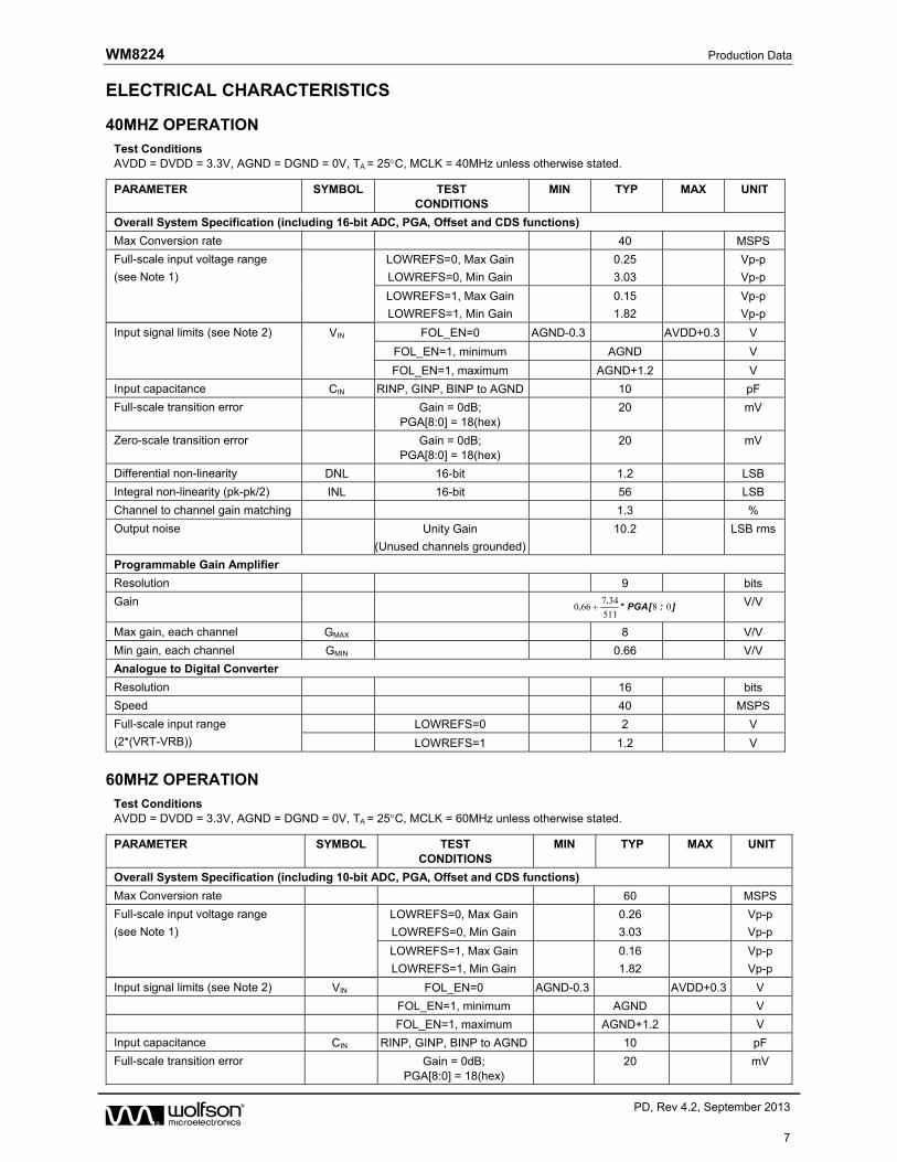
ELECTRICAL CHARACTERISTICS
40MHZ OPERATION
Test Conditions AVDD = DVDD = 3.3V, AGND = DGND = 0V, TA = 25C, MCLK = 40MHz unless otherwise stated.
PARAMETER SYMBOL TEST CONDITIONS
MIN TYP MAX UNIT
Overall System Specification (including 16-bit ADC, PGA, Offset and CDS functions)
Max Conversion rate 40 MSPS
Full-scale input voltage range
(see Note 1)
LOWREFS=0, Max Gain
LOWREFS=0, Min Gain
0.25
3.03
Vp-p
Vp-p
LOWREFS=1, Max Gain
LOWREFS=1, Min Gain
0.15
1.82
Vp-p
Vp-p
Input signal limits (see Note 2) VIN FOL_EN=0 AGND-0.3 AVDD+0.3 V
FOL_EN=1, minimum AGND V
FOL_EN=1, maximum AGND+1.2 V
Input capacitance CIN RINP, GINP, BINP to AGND 10 pF
Full-scale transition error Gain = 0dB; PGA[8:0] = 18(hex)
20 mV
Zero-scale transition error Gain = 0dB; PGA[8:0] = 18(hex)
20 mV
Differential non-linearity DNL 16-bit 1.2 LSB
Integral non-linearity (pk-pk/2) INL 16-bit 56 LSB
Channel to channel gain matching 1.3 %
Output noise Unity Gain
(Unused channels grounded)
10.2 LSB rms
Programmable Gain Amplifier
Resolution 9 bits
Gain ]:[PGA*.
. 08511
347660 V/V
Max gain, each channel GMAX 8 V/V
Min gain, each channel GMIN 0.66 V/V
Analogue to Digital Converter
Resolution 16 bits
Speed 40 MSPS
Full-scale input range
(2*(VRT-VRB))
LOWREFS=0 2 V
LOWREFS=1 1.2 V
60MHZ OPERATION
Test Conditions AVDD = DVDD = 3.3V, AGND = DGND = 0V, TA = 25C, MCLK = 60MHz unless otherwise stated.
PARAMETER SYMBOL TEST CONDITIONS
MIN TYP MAX UNIT
Overall System Specification (including 10-bit ADC, PGA, Offset and CDS functions)
Max Conversion rate 60 MSPS
Full-scale input voltage range
(see Note 1)
LOWREFS=0, Max Gain
LOWREFS=0, Min Gain
0.26
3.03
Vp-p
Vp-p
LOWREFS=1, Max Gain
LOWREFS=1, Min Gain
0.16
1.82
Vp-p
Vp-p
Input signal limits (see Note 2) VIN FOL_EN=0 AGND-0.3 AVDD+0.3 V
FOL_EN=1, minimum AGND V
FOL_EN=1, maximum AGND+1.2 V
Input capacitance CIN RINP, GINP, BINP to AGND 10 pF
Full-scale transition error Gain = 0dB; PGA[8:0] = 18(hex)
20 mV
WM8224 Production Data
w PD, Rev 4.2, September 2013
8
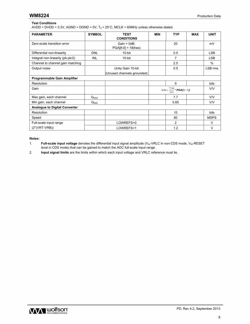
Test Conditions AVDD = DVDD = 3.3V, AGND = DGND = 0V, TA = 25C, MCLK = 60MHz unless otherwise stated.
PARAMETER SYMBOL TEST CONDITIONS
MIN TYP MAX UNIT
Zero-scale transition error Gain = 0dB; PGA[8:0] = 18(hex)
20 mV
Differential non-linearity DNL 10-bit 0.5 LSB
Integral non-linearity (pk-pk/2) INL 10-bit 7 LSB
Channel to channel gain matching 2.5 %
Output noise Unity Gain 10-bit
(Unused channels grounded)
0.5 LSB rms
Programmable Gain Amplifier
Resolution 9 bits
Gain ]:[PGA*.
. 08511
347660 V/V
Max gain, each channel GMAX 7.7 V/V
Min gain, each channel GMIN 0.65 V/V
Analogue to Digital Converter
Resolution 10 bits
Speed 60 MSPS
Full-scale input range
(2*(VRT-VRB))
LOWREFS=0 2 V
LOWREFS=1 1.2 V
Notes:
1. Full-scale input voltage denotes the differential input signal amplitude (VIN-VRLC in non-CDS mode, VIN-RESET level in CDS mode) that can be gained to match the ADC full-scale input range.
2. Input signal limits are the limits within which each input voltage and VRLC reference must lie.
WM8224 Production Data
w PD, Rev 4.2, September 2013
9
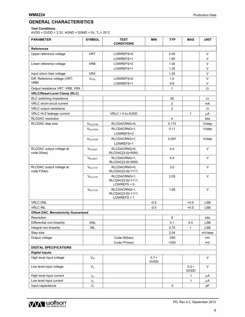
GENERAL CHARACTERISTICS
Test Conditions AVDD = DVDD = 3.3V, AGND = DGND = 0V, TA = 25C
PARAMETER SYMBOL TEST CONDITIONS
MIN TYP MAX UNIT
References
Upper reference voltage VRT LOWREFS=0
LOWREFS=1
2.05
1.85
V
V
Lower reference voltage VRB LOWREFS=0
LOWREFS=1
1.05
1.25
V
V
Input return bias voltage VRX 1.25 V
Diff. Reference voltage (VRT-VRB)
VRTB LOWREFS=0
LOWREFS=1
1.0
0.6
V
V
Output resistance VRT, VRB, VRX 1
VRLC/Reset-Level Clamp (RLC)
RLC switching impedance 50
VRLC short-circuit current 2 mA
VRLC output resistance 2
VRLC Hi-Z leakage current VRLC = 0 to AVDD 1 A
RLCDAC resolution 4 bits
RLCDAC step size
VRLCSTEP RLCDACRNG=0, 0.173 V/step
VRLCSTEP RLCDACRNG=1,
LOWREFS=0
0.11 V/step
VRLCSTEP RLCDACRNG=1,
LOWREFS=1
0.097 V/step
RLCDAC output voltage at code 0(hex)
VRLCBOT RLCDACRNG=0, RLCDAC[3:0]=0000,
0.4 V
VRLCBOT RLCDACRNG=1, RLCDAC[3:0]=0000,
0.4 V
RLCDAC output voltage at code F(hex)
VRLCTOP RLCDACRNG=0, RLCDAC[3:0]=1111,
3.0 V
VRLCTOP RLCDACRNG=1, RLCDAC[3:0]=1111,
LOWREFS = 0
2.05 V
VRLCTOP RLCDACRNG=1, RLCDAC[3:0]=1111,
LOWREFS = 1
1.85 V
VRLC DNL -0.5 +0.5 LSB
VRLC INL -0.5 +0.5 LSB
Offset DAC, Monotonicity Guaranteed
Resolution 8 bits
Differential non-linearity DNL 0.1 0.5 LSB
Integral non-linearity INL 0.75 1 LSB
Step size 2.04 mV/step
Output voltage Code 00(hex)
Code FF(hex)
-250
+250
mV
mV
DIGITAL SPECIFICATIONS
Digital Inputs
High level input voltage VIH 0.7 DVDD
V
Low level input voltage VIL 0.2 DVDD
V
High level input current IIH 1 A
Low level input current IIL 1 A
Input capacitance CI 5 pF

WM8224 Production Data
w PD, Rev 4.2, September 2013
10
Test Conditions AVDD = DVDD = 3.3V, AGND = DGND = 0V, TA = 25C
PARAMETER SYMBOL TEST CONDITIONS
MIN TYP MAX UNIT
Digital Outputs
High level output voltage VOH IOH = 1mA DVDD – 0.5
V
Low level output voltage VOL IOL = 1mA 0.5 V
High impedance output current IOZ 1 A
Digital IO Pins
Applied high level input voltage VIH 0.7 DVDD
V
Applied low level input voltage VIL 0.2 DVDD
V
High level output voltage VOH IOH = 1mA DVDD – 0.5
V
Low level output voltage VOL IOL = 1mA 0.5 V
Low level input current IIL 1 A
High level input current IIH 1 A
Input capacitance CI 5 pF
Output Impedance Ro Io = 1mA 38 Ω
High impedance output current IOZ 1 A
Supply Currents
Analogue supply current active FOL_EN=0 93 mA
FOL_EN=1 141 mA
Digital supply current active FOL_EN=0 7.3 mA
FOL_EN=1 8 mA
Total supply current active
FOL_EN=0 100.3 mA
FOL_EN=1 149 mA
Total supply current full power down mode
150 200 A

WM8224 Production Data
w PD, Rev 4.2, September 2013
11
INPUT VIDEO SAMPLING
CDS MODE (CDS=1)
Figure 1 Three-channel CDS Operation (CDS=1)
Figure 2 Two-channel CDS Operation (CDS=1)

WM8224 Production Data
w PD, Rev 4.2, September 2013
12
Figure 3 One-channel CDS Operation (CDS=1)
Notes:
1. The relationship between input video signal and sample points is controlled by VSMP and RSMP.
2. When VSMP is high the input video signal is connected to the Video sampling capacitors.
3. When RSMP is high the input video signal is connected to the Reset sampling capacitors.
4. Non-CDS operation is also possible; VSMP, MCLK timing is unchanged, RSMP is not required in this mode but can be
used to control input clamping.
NON-CDS MODE (CDS=0)
Figure 4 Three-channel non-CDS Operation (CDS=0)

WM8224 Production Data
w PD, Rev 4.2, September 2013
13
Figure 5 Two-channel non-CDS Operation (CDS=0)
Figure 6 One-channel non-CDS Operation (CDS=0)
Notes:
1. The relationship between input video signal and sample points is controlled by VSMP and RSMP.
2. When VSMP is high the input video signal is connected to the Video sampling capacitors and VRLC is connected to
the Reset sampling capacitors.
3. RSMP is not required in this mode but can be used to control input clamping.

WM8224 Production Data
w PD, Rev 4.2, September 2013
14
Test Conditions AVDD = DVDD = 3.3V, AGND = DGND = 0V, TA = 25C.
PARAMETER SYMBOL TEST CONDITIONS MIN TYP MAX UNITS
MCLK period, ACLKDIV=00 (default) tPER 12 or 16 bit 25 ns
tPER 8 or 10 bit 16.67 ns
MCLK high period tMCLKH 0.5 MCLK periods
MCLK low period tMCLKL 0.5 MCLK periods
MCLK Duty Cycle 45:55 55:45 %
RSMP pulse high time tRSD 3 ns
VSMP pulse high time tVSD 2 ns
RSMP falling to VSMP rising time tRSFVSR 0 ns
MCLK rising to VSMP rising time tMRVSR 3 ns
MCLK falling to VSMP falling time tMFVSF 7 ns
VSMP falling to MCLK rising time tVSFMR 0 ns
1st MCLK falling edge after VSMP falling to RSMP falling time
tMF1RSF 7 ns
3-channel mode pixel period tPR3 3 MCLK periods
2-channel mode pixel period tPR2 2 MCLK periods
1-channel mode pixel period tPR1 1 MCLK periods
Output latency. From 1st rising edge of MCLK after VSMP falling to data output
LAT OPDEL[3:0]=0000,
ACLKDIV=00
7 MCLK periods
Notes:
1. Parameters are measured at 50% of the rising/falling edge.
OUTPUT DATA TIMING
OEB
OPHi-Z
tPZE
Hi-Z
tPEZ
Figure 7 Output Enable/Disable Timing from OEB Pin
MCLK
OPHi-Z
tPDtPAEZ
Hi-Z
tPAZE
Figure 8 Output Enable/Disable Timing with AUTOZ=1
WM8224 Production Data
w PD, Rev 4.2, September 2013
15
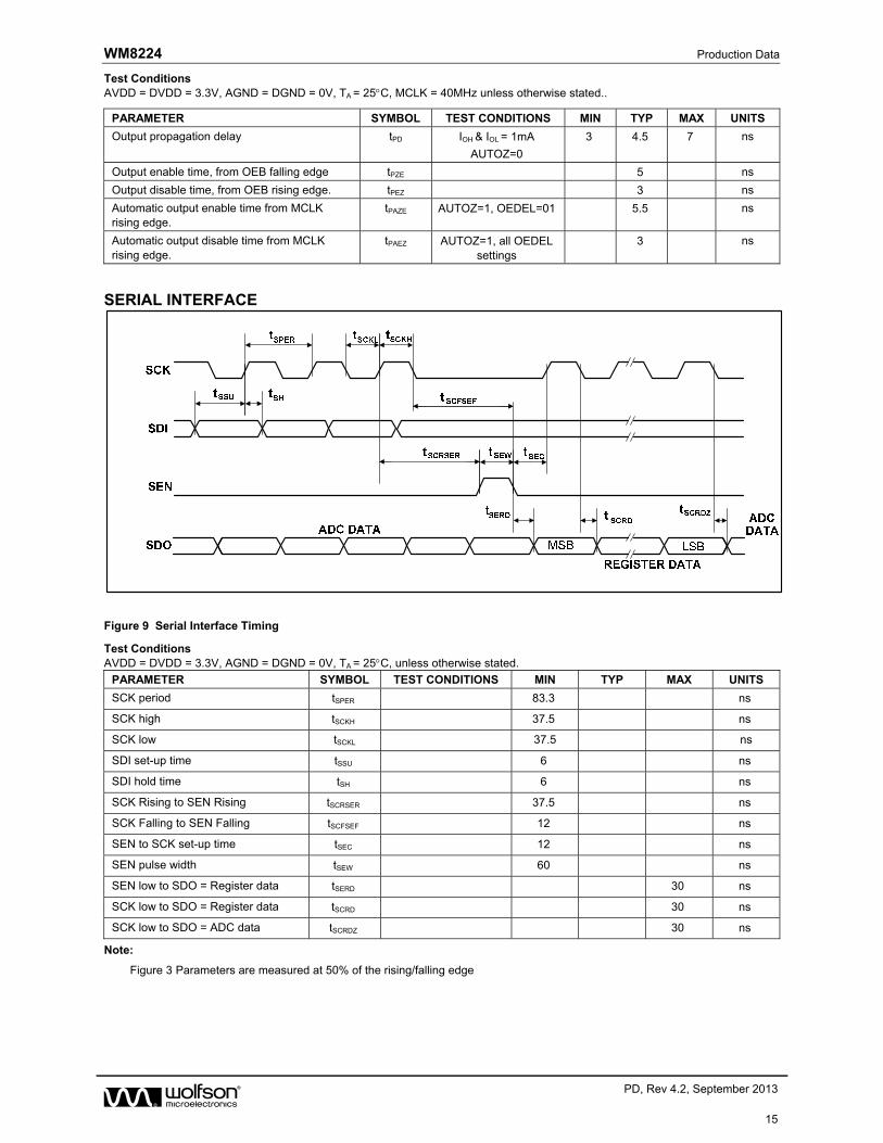
Test Conditions AVDD = DVDD = 3.3V, AGND = DGND = 0V, TA = 25C, MCLK = 40MHz unless otherwise stated..
PARAMETER SYMBOL TEST CONDITIONS MIN TYP MAX UNITS
Output propagation delay tPD IOH & IOL = 1mA
AUTOZ=0
3 4.5 7 ns
Output enable time, from OEB falling edge tPZE 5 ns
Output disable time, from OEB rising edge. tPEZ 3 ns
Automatic output enable time from MCLK rising edge.
tPAZE AUTOZ=1, OEDEL=01 5.5 ns
Automatic output disable time from MCLK rising edge.
tPAEZ AUTOZ=1, all OEDEL settings
3 ns
SERIAL INTERFACE
Figure 9 Serial Interface Timing
Test Conditions AVDD = DVDD = 3.3V, AGND = DGND = 0V, TA = 25C, unless otherwise stated.
PARAMETER SYMBOL TEST CONDITIONS MIN TYP MAX UNITS
SCK period tSPER 83.3 ns
SCK high tSCKH 37.5 ns
SCK low tSCKL 37.5 ns
SDI set-up time tSSU 6 ns
SDI hold time tSH 6 ns
SCK Rising to SEN Rising tSCRSER 37.5 ns
SCK Falling to SEN Falling tSCFSEF 12 ns
SEN to SCK set-up time tSEC 12 ns
SEN pulse width tSEW 60 ns
SEN low to SDO = Register data tSERD 30 ns
SCK low to SDO = Register data tSCRD 30 ns
SCK low to SDO = ADC data tSCRDZ 30 ns
Note:
Figure 3 Parameters are measured at 50% of the rising/falling edge

WM8224 Production Data
w PD, Rev 4.2, September 2013
16
INTERNAL POWER ON RESET CIRCUIT
Figure 10 Internal Power On Reset Circuit Schematic
The WM8224 includes an internal Power-On-Reset Circuit, as shown in Figure 10, which is used to reset the digital logic into a default state after power up. The POR circuit is powered from AVDD and monitors DVDD. It asserts PORB low if AVDD or DVDD is below a minimum threshold.
DVDD
AVDD
Vpord_on
DGND
AGND
Internal POR active
LO
HI
Device ReadyInternalPOR active
No PowerPORUndefined
Vpora_off
Vpora
INTERNAL PORB
Figure 11 Typical Power up Sequence where AVDD is Powered before DVDD
Figure 11 shows a typical power-up sequence where AVDD is powered up first. When AVDD rises above the minimum threshold, Vpora, there is enough voltage for the circuit to guarantee PORB is asserted low and the chip is held in reset. In this condition, all writes to the control interface are ignored. Now AVDD is at full supply level. Next DVDD rises to Vpord_on and PORB is released high and all registers are in their default state and writes to the control interface may take place.
On power down, where AVDD falls first, PORB is asserted low whenever AVDD drops below the minimum threshold Vpora_off.
Figure 12 Typical Power up Sequence where DVDD is Powered before AVDD

WM8224 Production Data
w PD, Rev 4.2, September 2013
17
Figure 12 shows a typical power-up sequence where DVDD is powered up first. First it is assumed that DVDD is already up to specified operating voltage. When AVDD goes above the minimum threshold, Vpora, there is enough voltage for the circuit to guarantee PORB is asserted low and the chip is held in reset. In this condition, all writes to the control interface are ignored. When AVDD rises to Vpora_on, PORB is released high and all registers are in their default state and writes to the control interface may take place.
On power down, where DVDD falls first, PORB is asserted low whenever DVDD drops below the minimum threshold Vpord_off.
SYMBOL MIN TYP MAX UNIT
Vpora 0.4 0.6 0.8 V
Vpora_on 0.9 1.2 1.6 V
Vpora_off 0.4 0.6 0.8 V
Vpord_on 0.5 0.7 0.9 V
Vpord_off 0.4 0.6 0.8 V
Table 1 Typical POR Operation (typical values, not tested)
Note: It is recommended that every time power is cycled to the WM8224 a software reset is written to the software register to ensure that the contents of the control registers are at their default values before carrying out any other register writes.
WM8224 Production Data
w PD, Rev 4.2, September 2013
18
DEVICE DESCRIPTION
INTRODUCTION
A block diagram of the device showing the signal path is presented on the front page of this datasheet.
The WM8224 samples up to three inputs (RINP, GINP and BINP) simultaneously. The device then processes the sampled video signal with respect to the video reset level or an internally/externally generated reference level using between one and three processing channels.
Each processing channel consists of an Input Sampling block with optional Reset Level Clamping (RLC) and Correlated Double Sampling (CDS), an 8-bit programmable offset DAC and a 9-bit Programmable Gain Amplifier (PGA).
The processing channel outputs are switched alternately by a 3:1 multiplexer to the ADC input.
The ADC then converts each resulting analogue signal to a digital word. The digital output from the ADC is presented in a variety of possible output formats onto the output bus, OP[11:0]. The twelve output pins can be set to a high impedance state using either the OEB control pin or the OPD register bit.
On-chip control registers determine the configuration of the device, including the offsets and gains applied to each channel. These registers are programmable via a serial interface.
The device has a Black-Level Calibration function which allows the D.C. offset determined during the optically-black pixels at the beginning of the linear sensor to be removed during the image-pixels.
CONFIGURABLE RESOLUTION OF ADC
The WM8224 has a configurable ADC resolution. The default setting is 16 bits resolution. This can be changed by the user by changing a register setting.
The register RES[1:0] can be changed to alter the resolution from 16 bits to either 12, 10 or 8 bits resolution.
INPUT SAMPLING
The WM8224 can sample and process up to three inputs through one to three processing channels as follows:
Colour Pixel-by-Pixel: The three inputs (RINP, GINP and BINP) are simultaneously sampled for each pixel and a separate channel processes each input. The signals are then multiplexed into the ADC, which converts all three inputs within the pixel period.
Two Channel Pixel-by-pixel: Two input channels (RINP and GINP, RINP and BINP, or GINP and BINP) are simultaneously sampled for each pixel and a separate channel processes each input. The signals are then multiplexed into the ADC, which converts both inputs within the pixel period. The unused channel can be changed via the control interface. The unused channel is powered down when this mode is selected.
Monochrome: A single chosen input (RINP, GINP, or BINP) is sampled, processed by the corresponding channel, and converted by the ADC. The choice of input channel can be changed via the control interface. The unused channels are powered down when this mode is selected.

WM8224 Production Data
w PD, Rev 4.2, September 2013
19
RESET LEVEL CLAMPING (RLC)
To ensure that the signal applied to the WM8224 lies within the supply voltage range (0V to AVDD) the output signal from a CCD is usually level shifted by coupling through a capacitor, CIN. The RLC circuit clamps the WM8224 side of this capacitor to a suitable voltage through a CMOS switch during the CCD reset period (pixel clamping) or during the black pixels (line clamping). In order for clamping to produce correct results the input voltage during the clamping must be a constant value.
Note that if the ac coupling capacitor (CIN) is used in non-CDS mode (CDS=0), then to minimise code drift, line clamping should be used and internal input voltage buffers enabled using the FOL_EN register bit. Alternatively, if the input signal contains a stable reference/reset level then pixel clamping should be used, and the voltage buffers need not be enabled.
The WM8224 allows the user to control the RLC switch in a variety of ways as illustrated in Figure 13. This figure shows a single channel, however all 3 channels are identical, each with its own clamp switch controlled by the common CLMP signal.
The method of control chosen depends upon the characteristics of the input video. The RLCEN register bit must be set to 1 to enable clamping, otherwise the RLC switch cannot be closed (by default RLCEN=1).
Note that unused inputs should be left floating, or grounded through a decoupling capacitor, if reset level clamping is used.
Figure 13 RLC Clamp Control Options
When an input waveform has a stable reference level on every pixel it may be desirable to clamp every pixel during this period. Setting CLMPCTRL=0 means that the RLC switch is closed whenever the RSMP input pin is high, as shown in Figure 14.
MCLK
VSMP
RSMP
RLC switch control"CLMP"
(RLCEN=1,CLMPCTRL=0)
RLC switch closedwhen RSMP=1
Video sample taken onfallling edge of VSMP
Reset/reference sample takenon fallling edge of RSMP
INPUT VIDEOSIGNAL
reference("black") level
video level
Figure 14 Reset Level Clamp Operation (CLMPCTRL=0), CDS operation shown, non-CDS also possible

WM8224 Production Data
w PD, Rev 4.2, September 2013
20
In situations where the input video signal does not have a stable reference level it may be necessary to clamp only during those pixels which have a known state (e.g. the dummy, or “black” pixels at the start or end of a line on most image sensors). This is known as line-clamping and relies on the input capacitor to hold the DC level between clamp intervals. In non-CDS mode (CDS=0) this can be done directly by controlling the RSMP input pin to go high during the black pixels only. Note that internal input voltage buffers should be enabled using the FOL_EN register bit when using this mode of operation.
Alternatively it is possible to use RSMP to identify the black pixels and enable the clamp at the same time as the input is being sampled (i.e. when VSMP is high and RSMP is high). This mode is enabled by setting CLMPCTRL=1 and the operation is shown in Figure 15.
MCLK
VSMP
RSMP
RLC switch control,"CLMP"
(RLCEN=1,CLMPCTRL=1)
RLC switch closed when RSMP=1 &&VSMP=1 (during "black" pixels)
Video and reference sampletaken on fallling edge of VSMP
INPUT VIDEOSIGNAL
unstablereference level dummy or
"black" pixel
video level
Figure 15 Reset Level Clamp Operation (CLMPCTRL=1), non-CDS mode only
RLCEN CLAMPCTRL OUTCOME USE
0 X RLC is not enabled. RLC switch is always open. When input is DC coupled and within supply rails.
1 0 RLC switch is controlled directly from RSMP input pin:
RSMP=0: switch is open
RMSP=1: switch is closed
When ASIC explicitly provides a reset sample signal and the input video waveform has a suitable reset level.
1 1 VSMP applied as normal, RSMP is used to indicate the location of black pixels
RLC switch is controlled by logical combination of RSMP and VSMP:
RSMP && VSMP = 1: switch is closed
Switch is re-opened when:
VSMP=0 (non-CDS mode)
VSMP=0 and RSMP=0 (CDS mode)
When clamping during the video period of black pixels or there is no stable per-pixel reference level.
This method of operation is generally only sensible in non-CDS mode.
Table 2 Reset Level Clamp Control Summary
WM8224 Production Data
w PD, Rev 4.2, September 2013
21
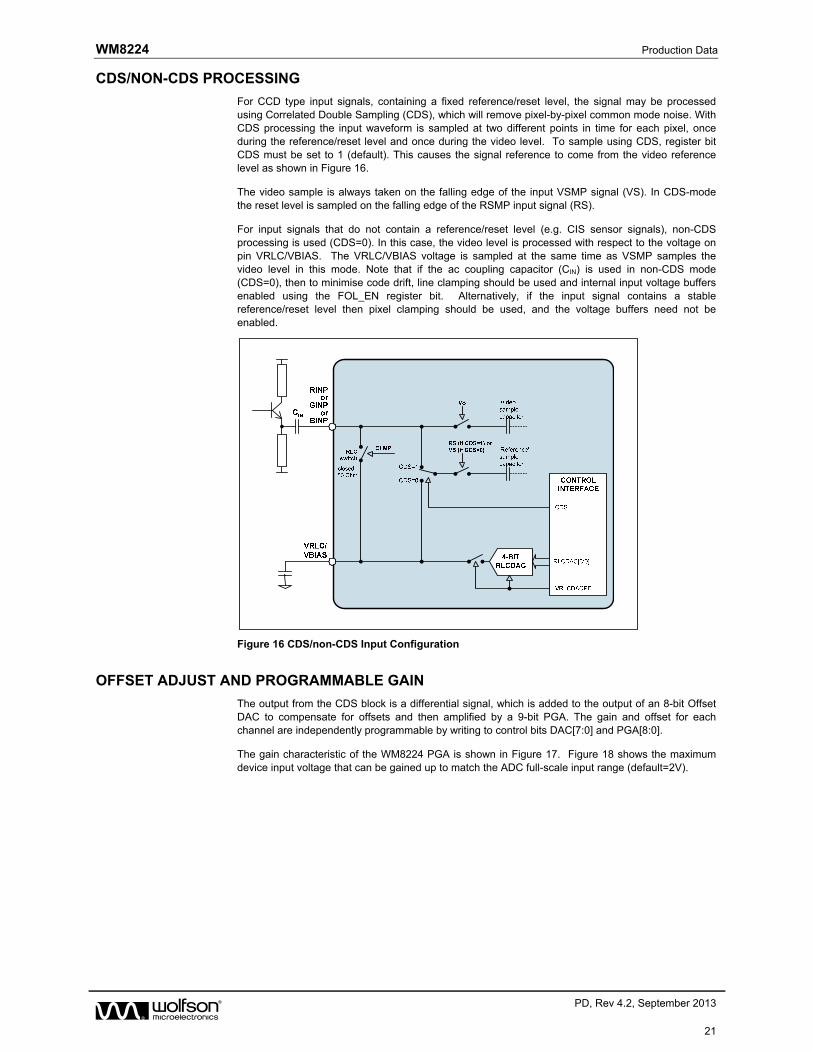
CDS/NON-CDS PROCESSING
For CCD type input signals, containing a fixed reference/reset level, the signal may be processed using Correlated Double Sampling (CDS), which will remove pixel-by-pixel common mode noise. With CDS processing the input waveform is sampled at two different points in time for each pixel, once during the reference/reset level and once during the video level. To sample using CDS, register bit CDS must be set to 1 (default). This causes the signal reference to come from the video reference level as shown in Figure 16.
The video sample is always taken on the falling edge of the input VSMP signal (VS). In CDS-mode the reset level is sampled on the falling edge of the RSMP input signal (RS).
For input signals that do not contain a reference/reset level (e.g. CIS sensor signals), non-CDS processing is used (CDS=0). In this case, the video level is processed with respect to the voltage on pin VRLC/VBIAS. The VRLC/VBIAS voltage is sampled at the same time as VSMP samples the video level in this mode. Note that if the ac coupling capacitor (CIN) is used in non-CDS mode (CDS=0), then to minimise code drift, line clamping should be used and internal input voltage buffers enabled using the FOL_EN register bit. Alternatively, if the input signal contains a stable reference/reset level then pixel clamping should be used, and the voltage buffers need not be enabled.
Figure 16 CDS/non-CDS Input Configuration
OFFSET ADJUST AND PROGRAMMABLE GAIN
The output from the CDS block is a differential signal, which is added to the output of an 8-bit Offset DAC to compensate for offsets and then amplified by a 9-bit PGA. The gain and offset for each channel are independently programmable by writing to control bits DAC[7:0] and PGA[8:0].
The gain characteristic of the WM8224 PGA is shown in Figure 17. Figure 18 shows the maximum device input voltage that can be gained up to match the ADC full-scale input range (default=2V).

WM8224 Production Data
w PD, Rev 4.2, September 2013
22
0
1
2
3
4
5
6
7
8
0 128 256 384 512
Gain Code (PGA[8:0])
PG
A G
ain
(V
/V)
0
0.5
1
1.5
2
2.5
3
3.5
0 128 256 384 512Gain Code (PGA[8:0])
Inp
ut
Vo
ltag
e R
ang
e (V
)
Max i/p VoltageLOWREFS=0
Max i/p VoltageLOWREFS=1
Figure 17 PGA Gain Characteristic Figure 18 Peak Input Voltage to Match ADC Full-scale Range
ADC INPUT BLACK LEVEL ADJUST
The output from the PGA can be offset to match the full-scale range of the differential ADC (2*[VRT-VRB]).
For negative-going input video signals, a black level (zero differential) output from the PGA should be offset to the top of the ADC range by setting register bits PGAFS[1:0]=10. This will give an output code of FFFF (hex) from the WM8224 for zero input. If code zero is required for zero differential input then the INVOP bit should be set.
For positive going input signals the black level should be offset to the bottom of the ADC range by setting PGAFS[1:0]=11. This will give an output code of 0000 (hex) from the WM8224 for zero input.
Bipolar input video is accommodated by setting PGAFS[1:0]=00 or PGAFS[1:0]=01. Zero differential input voltage gives mid-range ADC output, 7FFF (hex).

WM8224 Production Data
w PD, Rev 4.2, September 2013
23
Figure 19 ADC Input Black Level Adjust Settings
OVERALL SIGNAL FLOW SUMMARY
Figure 20 represents the processing of the video signal through the WM8224.
VRESET
VVRLC
V3
CDS = 1
CDS = 0
CDACPD=1
250mV*(DAC[7:0]-127.5)/127.5
analog-
X++
See parametrics for DAC voltages.
OP pins
D1
digital
ADC BLOCKPGABLOCK
OFFSET DACBLOCK
INPUTSAMPLING
BLOCK D2
CDS, CDACPD,CDAC[3:0], DAC[7:0], PGA[8:0], PGAFS[1:0] and INVOP are set by programming internal control registers.CDS=1 for CDS, 0 for non-CDS
VIN is RINP or GINP or BINPVRESET is VIN sampled during reset clampVRLC is voltage applied to VRLC/VBIAS pin
VIN
x (65535/VFS)+0 if PGAFS[1:0]=11+65535 if PGAFS[1:0]=10+32768 if PGAFS[1:0]=0x
PGA gainA= 0.66+PGA[8:0]x7.34/511
OUTPUTINVERTBLOCK
D2 = D1 if INVOP = 0D2 = 65535-D1 if INVOP = 1
OffsetDAC
RLCDAC
+
V2V1
CDACPD=0
Figure 20 Overall Signal Flow
The INPUT SAMPLING BLOCK produces an effective input voltage V1. For CDS, this is the difference between the input video level VIN and the input reset level VRESET. For non-CDS this is the difference between the input video level VIN and the voltage on the VRLC/VBIAS pin, VVRLC, optionally set via the RLC DAC.
The OFFSET DAC BLOCK then adds the amount of fine offset adjustment required to move the black level of the input signal towards 0V, producing V2.
The PGA BLOCK then amplifies the white level of the input signal to maximise the ADC range, outputting voltage V3.
The ADC BLOCK then converts the analogue signal, V3, to a 16-bit unsigned digital output, D1.
The digital output is then inverted, if required, through the OUTPUT INVERT BLOCK to produce D2.

WM8224 Production Data
w PD, Rev 4.2, September 2013
24
CALCULATING THE OUTPUT CODE FOR A GIVEN INPUT
The following equations describe the processing of the video and reset level signals through the WM8224.
INPUT SAMPLING BLOCK: INPUT SAMPLING AND REFERENCING
If CDS = 1, (i.e. CDS operation) the previously sampled reset level, VRESET, is subtracted from the input video, VIN (= RINP, GINP or BINP).
V1 = VIN – VRESET Eqn. 1
If CDS = 0, (non-CDS operation) the simultaneously sampled voltage on pin VRLC is subtracted instead.
V1 = VIN – VVRLC Eqn. 2
If VRLCDACPD = 1, VVRLC is an externally applied voltage on pin VRLC/VBIAS.
If VRLCDACPD = 0, VVRLC is the output from the internal RLC DAC.
VVRLC = (VRLCSTEP RLC DAC[3:0]) + VRLCBOT Eqn. 3
VRLCSTEP is the step size of the RLC DAC and VRLCBOT is the minimum output of the RLC DAC.
OFFSET DAC BLOCK: OFFSET (BLACK-LEVEL) ADJUST
The resultant signal V1 is added to the Offset DAC output.
V2 = V1 + 250mV (DAC[7:0]-127.5) / 127.5 Eqn. 4
PGA NODE: GAIN ADJUST
The signal is then multiplied by the PGA gain.
V3 = V2 (0.66 + PGA[8 :0]x7.34/511) Eqn. 5
ADC BLOCK : ANALOGUE-DIGITAL CONVERSION
The analogue signal is then converted to a 16-bit unsigned number, with input range configured by PGAFS[1:0].
D1[15:0] = INT (V3 /VFS) 65535 + 32767 PGAFS[1:0] = 00 or 01 Eqn. 6
D1[15:0] = INT (V3 /VFS) 65535 PGAFS[1:0] = 11 Eqn. 7
D1[15:0] = INT (V3 /VFS) 65535 + 65535 PGAFS[1:0] = 10 Eqn. 8
where the ADC full-scale range, VFS = 2V when LOWREFS=0 and VFS = 1.2V when LOWREFS=1.
OUTPUT INVERT BLOCK: POLARITY ADJUST
The polarity of the digital output may be inverted by control bit INVOP.
D2[15:0] = D1[15:0] (INVOP = 0) Eqn. 9
D2[15:0] = 65535 – D1[15:0] (INVOP = 1) Eqn. 10
WM8224 Production Data
w PD, Rev 4.2, September 2013
25
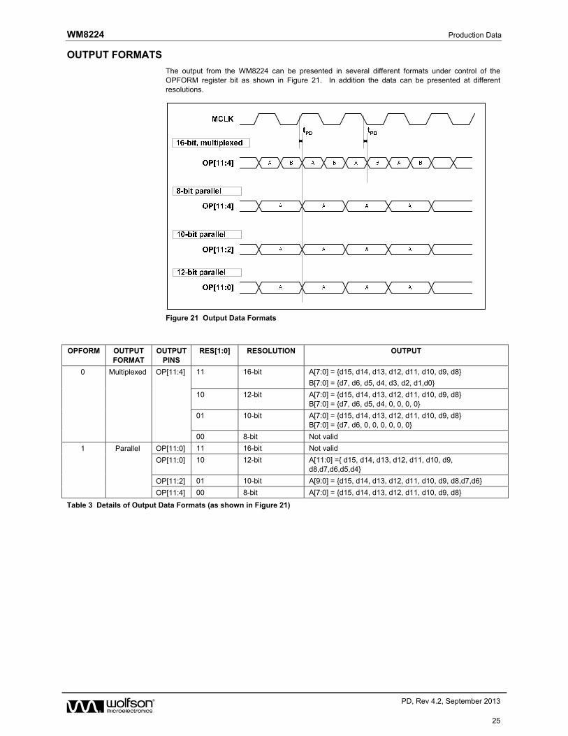
OUTPUT FORMATS
The output from the WM8224 can be presented in several different formats under control of the OPFORM register bit as shown in Figure 21. In addition the data can be presented at different resolutions.
Figure 21 Output Data Formats
OPFORM OUTPUT
FORMAT OUTPUT
PINS RES[1:0] RESOLUTION OUTPUT
0 Multiplexed OP[11:4] 11 16-bit A[7:0] = d15, d14, d13, d12, d11, d10, d9, d8
B[7:0] = d7, d6, d5, d4, d3, d2, d1,d0
10 12-bit A[7:0] = d15, d14, d13, d12, d11, d10, d9, d8 B[7:0] = d7, d6, d5, d4, 0, 0, 0, 0
01 10-bit A[7:0] = d15, d14, d13, d12, d11, d10, d9, d8 B[7:0] = d7, d6, 0, 0, 0, 0, 0, 0
00 8-bit Not valid
1 Parallel OP[11:0] 11 16-bit Not valid
OP[11:0] 10 12-bit A[11:0] = d15, d14, d13, d12, d11, d10, d9, d8,d7,d6,d5,d4
OP[11:2] 01 10-bit A[9:0] = d15, d14, d13, d12, d11, d10, d9, d8,d7,d6
OP[11:4] 00 8-bit A[7:0] = d15, d14, d13, d12, d11, d10, d9, d8
Table 3 Details of Output Data Formats (as shown in Figure 21)

WM8224 Production Data
w PD, Rev 4.2, September 2013
26
PROGRAMMABLE AUTOMATIC BLACK LEVEL CALIBRATION
The Programmable Automatic Black-Level Calibration (BLC) function is to adjust the D.C. offset of the output data such that the digital output code for black pixels is calibrated to a target black level value. The D.C. offset is determined during the optically-black pixels at the beginning of the linear sensor, and removed during the image-pixels as shown in Figure 22.
Black Pixel Period Image Pixel Period
Determine Black Level Offset
Remove Black Level Offset from Image Pixels
Figure 22 Linear Sensor Model
The automatic black level calibration operates assuming 12 bits ADC resolution. Adjustments to calculations must be made for different ADC resolutions.
The black level calibration process occurs in two stages as shown in Figure 23 below:
Coarse Adjust Calibration: This is a mixed signal loop which removes the coarse offset by adjusting the offset DAC.
Fine Adjust Calibration: This is a digital loop which removes the remaining offset with better noise tolerance, utilising ADC over-range to improve the dynamic range of the system.
TARGET BL
Input Black Level V1Adjusted
ADC OutputPGA ADC
Offset DAC
Mixed Signal LOOPDigits
Coarse Adjust Calibration
Fine Adjust Calibration
Digital LOOPDigits
Figure 23 BLC Top-Level Circuitry
TARGET CODES
The user must specify a target black level for each Red, Green and Blue channel through the registers TARGETR, TARGETG and TARGETB. If, during the black-pixel period, the average ADC output code was, for example, 100 and the user specified the target black level code to be 10, the BLC circuitry would determine 90 codes should be subtracted from the ADC output. These 90 codes will then be subtracted from every image-pixel code output from the ADC.
Note – changing the PGA gain affects the black-level through the device; the gain should therefore not be changed during a BLC procedure. If the PGA gain changes, then the BLC routine should be re-run.
The automatic black level calibration feature operates with the assumption of a 12bit ADC resolution. The register settings for Target Codes (TARGETx[7:0]) should be set differently depending on the

WM8224 Production Data
w PD, Rev 4.2, September 2013
27
ADC resolution being used. As TARGETx[7:0] is an 8 bit register, the 4 MSBs of a data output code cannot be changed.
16bit ADC Resolution
For 16bit resolution the target code entered into TARGETx[7:0] will ignore the 4 MSBs and 4 LSBs of the 16-bit data output. For example if the desired code out is 0000111111110001, the value entered into TARGETx[7:0] would be 11111111.
12bit ADC Resolution
For 12bit resolution the 4 MSBs of the 12 bit data output code will be ignored. For example if the desired code out is 000011111111, the value entered into TARGETx[7:0] would be 11111111.
10bit ADC Resolution
For 10bit resolution the 4 MSBs of the 10bit data output code will be ignored. The 2 LSBs of the target code should be set to ‘00’. For example if the desired code out is 0000111111, the value entered into TARGETx[7:0] would be 11111100.
8bit ADC Resolution
For 8bit resolution the 4 MSBs of the 8bit data output code will be ignored. The 4 LSBs of the target code should be set to ‘0000’. For example if the desired code out is 00001111, the value entered into TARGETx[7:0] would be 11110000.
INDICATING THE START OF A BLC PROCEDURE
The start of a line is required to be indicated to the WM8224 to allow the black-pixel period to be located. This can be achieved by two methods. The register TG_METHOD is set to reflect which method is to be used.
METHOD 1: OEB PIN
The OEB pin can be shared with the BLC function to indicate the start of a line if the OEB functionality is not required. To indicate the start of a line, send a line synchronisation pulse, TG, on the OEB pin. It must be high for at least one rising edge of MCLK. The TG_METHOD register must be set to either ‘10’ or ‘11’ depending on whether positive or negative edge triggering is required, as shown in Figure 24.
Figure 24 Start of Line Indicator Using TG on the OEB Pin

WM8224 Production Data
w PD, Rev 4.2, September 2013
28
METHOD 2: REGISTER WRITE
The start of a line can also be indicated using a register write to TG_REG. The first rising edge of MCLK after TG_REG goes high will indicate the start of the line. TG_REG shall be automatically set to zero by the device. This process can be repeated to indicate the start of a second line, as shown in Figure 25. Set TG_METHOD to ‘00’
Figure 25 Start of Line Indicator Using TG_REG
BLC DURATION CONTROL
DUMMY PIXEL DELAY
Once the start of line has been determined there can be a delay to allow for the dummy pixels at the start of the sensor to be ignored. This is controlled by BLC_DEL, which is the number of pixels there should be between the start of line indicator and the start of the BLC routine.
The register BPIX_AVAIL must also be set up for the number of black pixels available to carry out the calibration. The durations of the Coarse Adjust Calibration and Fine Adjust calibration can then be determined as detailed below.
Figure 26 BLC Duration Control
COARSE ADJUST CALIBRATION ITERATION DURATION
The duration of one iteration of the Coarse Adjust is an integer number of VSMP periods. The exact number of VSMP periods depends on the MCLK:VSMP ratio and the number of channels used. The implementation ensures that there are at least a certain number of MCLK’s per Coarse Adjust iteration as shown in Table 4.

WM8224 Production Data
w PD, Rev 4.2, September 2013
29
MODE MINIMUM NO. OF MCLKS PER COARSE ADJUST ITERATION
3-Channel 11
2-Channel 10
Mono 9
Table 4 Modes vs MCLKs for Coarse Iterations
The BLC design rounds the Coarse Adjust iteration duration up to a whole number of pixels (i.e. the iteration duration will be a whole number of VSMP periods).
FINE ADJUST CALIBRATION DURATION
The Fine Adjust calibration duration is determined by the number of remaining black pixels after the coarse adjust has taken place.
BLC TEST MODE
This mode allows the status of the BLC to be seen on the 2 LSBs of the output data pins OP[1:0]. This mode could be enabled during the setup stage of the device to ensure that the black level calibration does not encroach on the active pixel data. Set the STATEOUT register to enable this mode. Once the BLC register values have been determined this register should be disabled. Table 5 shows the description of the output data.
DATA ON OP[1:0] DESCRIPTION
00 No BLC
01 Dummy Pixels
10 Coarse Adjust Calibration
11 Fine Adjust Calibration
Table 5 Test Mode Outputs
BLC WORKED EXAMPLE:
Below is an example of how to configure the WM8224 for Black Level Calibration.
Assumptions
MCLK frequency = 40MHz
VSMP frequency = 13.33MHz
Mode of operation = 3 Channel Mode
Black pixels on sensor = 50
Dummy pixels on sensor = 20
The following stages set up the Black Level calibration although not all stages may be required depending on the application:
1. Set up the Dummy Pixel Delay
2. Define the Coarse Adjust Calibration
3. Define the Fine Adjust Calibration

WM8224 Production Data
w PD, Rev 4.2, September 2013
30
1. Dummy Pixel delay
Set BLC_DEL, the number of dummy pixels for the sensor
BLC_DEL = ‘0010100’
The duration for this will then be BLC_DEL * VSMP period
Dummy pixel delay = 20*75ns = 1.5us
2. Define the coarse adjust loop
When setting the coarse adjust calibration it is necessary to bear in mind the following:
The number of black pixels available
The coarse adjust iteration duration
The number of iterations required.
Step 1: Set up BPIX_AVAIL with the number of available black pixels for the sensor.
BPIX_AVAIL = ’0000110010’
Step 2: Calculate MCLK:VSMP ratio
40:13.33 = 3:1
Step 3: Calculate the duration of the iteration in no. of pixels (round up value). Refer to Table 4 for the number of MCLK’s per Coarse Adjust iteration
Round up this value to give the no of pixels per iteration
= 4 pixels per iteration
Note: The device will automatically calculate this value.
Step 4: Set the register CADUR for max number of iterations.
CADUR = 2
Theoretically there can be 7 coarse adjust iterations during the black pixel period. However, in most cases 2 would be sufficient depending on the number of black pixels available to allow time for the fine adjust loop.
3. Fine Adjust Calibration
Step 1: Enable Register FA_EN to allow for fine adjust calibration
Step 2: The time available for fine adjustment is determined by the no. of remaining black pixels after the coarse adjust has taken place.
BPIX_AVAIL – (CADUR* iteration duration)
50 – (2*4)
= 42 pixels
pixelsofnoratioVSMPMCLK
MCLKsofno.
):(
.
67.33
11
):(
.
ratioVSMPMCLK
MCLKsofno

WM8224 Production Data
w PD, Rev 4.2, September 2013
31
BLC SCENARIOS OF OPERATION
The BLC can be used in various ways to suit the application, for example calibration can be done once per page or once per line. Register set up should be carried out before the start of a frame and is not required to be done on a line by line basis if using the Method 1 OEB PIN method. Five potential scenarios of operation are suggested below.
Note: The registers FRAME_START and SEQ_START when set high by the user will automatically be set low by the device.
SCENARIO 1
Coarse Adjust Calibration enabled for the 1st line, Fine Adjust Calibration enabled every line with the Fine Adjust Calibration result recalculated every line. This scenario is suitable for dealing with large amounts of d.c. drift throughout a frame; but this is at a cost of potential line-by-line variation in the Fine Adjust result (dependent on sensor noise and the PGA gain). Table 6 shows which registers are required for this scenario with example settings.
SETUP REGISTER
BPIX_AVAIL CADUR FRAME_START FA_EVERYLINE
Value 50 2 1 1
Table 6 Example Register Settings for Scenario 1
Figure 27 Scenario 1

WM8224 Production Data
w PD, Rev 4.2, September 2013
32
SCENARIO 2
Coarse Adjust and Fine Adjust Calibration enabled for the 1st line, with the Fine Adjust result updated on the 1st line only. This scenario is suitable for adjusting for black-level d.c. drift on a frame-by-frame basis; there will be no line-by-line variation in the black-level from the BLC circuitry. Table 7 shows which registers are required for this scenario with example settings.
SETUP REGISTER
BPIX_AVAIL CADUR FRAME_START
Value 50 2 1
Table 7 Example Register Settings for Scenario 2
Figure 28 Scenario 2
SCENARIO 3
Coarse Adjust Calibration enabled for the 1st line, Fine Adjust Calibration enabled every line with the Fine Adjust result accumulated throughout frame and used every line. This scenario allows any variation in the black-level to be tracked throughout the frame by accumulating the Fine Adjust result over multiple lines. This method does not deal with as large amounts of d.c. drift throughout the frame as scenario 1, but it will produce less line-by-line variation. Table 8 shows which registers are required for this scenario with example settings.
SETUP REGISTER
BPIX_AVAIL CADUR FRAME_START FA_EVERYLINE FA_ACCUM
Value 50 2 1 1 1
Table 8 Example Register Settings for Scenario 3
Figure 29 Scenario 3

WM8224 Production Data
w PD, Rev 4.2, September 2013
33
SCENARIO 4
Coarse Adjust Calibration enabled for 1st line, Fine Adjust Calibration enabled every line with the Fine Adjust result accumulated throughout frame and used at start of next frame. This scenario is intended to be used with a sequence of multiple frames, the first frame being used as a calibration frame. This is good for use with sensors containing very few black-pixels as the black-level offset can be calculated over an entire frame and there will be no line-by-line variation in the black-level from the BLC circuitry. Table 9 shows which registers are required for this scenario with example settings.
SETUP REGISTER
BPIX_AVAIL CADUR FRAME_START FRAME_SEQ SEQ_START FA_EVERYLINE FA_ACCUM
Value 50 2 1 1 1 1 1
Table 9 Example Register Settings for Scenario 4
Figure 30 Scenario 4

WM8224 Production Data
w PD, Rev 4.2, September 2013
34
SCENARIO 5
This scenario utilises the information from a possible calibration black-strip at the start of a scan. The register LINE_DEL sets the number of lines from the start of the frame that the BLC procedure is to be performed, so as to coincide with the calibration strip. Table 10 shows which registers are required for this scenario with example settings.
SETUP REGISTER BPIX_AVAIL CADUR LINE_DEL FRAME_START FA_EVERYLINE
Value 1000 2 50 1 1
Table 10 Example Register Settings for Scenario 5
Figure 31 Scenario 5

WM8224 Production Data
w PD, Rev 4.2, September 2013
35
REFERENCES
The ADC reference voltages are derived from an internal bandgap reference, and buffered to pins VRT and VRB, where they must be decoupled to ground. Pin VRX is driven by a similar buffer, and also requires decoupling. The output buffer from the RLCDAC also requires decoupling at pin VRLC/VBIAS.
The ADC references can be switched from the default values (VRT=2.05V, VRB=1.05V, ADC input range=2V) to give a smaller ADC reference range (VRT=1.85V, VRB=1.25V, ADC input range=1.2V) under control of the LOWREFS register bit. Setting LOWREFS=1 allows smaller input signals to be accommodated.
Note:
When LOWREFS = 1 the output of the RLCDAC will scale if RLCDACRNG = 1. The max output from RLCDAC will change from 2.05 to 1.85V and the step size will proportionally reduce.
POWER MANAGEMENT
Power management for the device is performed via the Control Interface. By default the device is fully enabled. The EN bit allows the device to be fully powered down when set low. Individual blocks can be powered down using the bits in Setup Register 5. When in MONO or TWOCHAN mode the unused input channels are automatically disabled to reduce power consumption.
Note:
1. It is recommended that if the clocks are removed from the device, the device should be powered down using the EN bit in Setup Reg 1.
2. It is recommended that when the device is powered up after powered down using the EN bit Setup Reg 1, PGA gain setting should be set to default. Alternatively if PGA gain is not default, the following sequence can be applied after powered up using EN bit.
i. Setup Reg 6, bit[0] (RESET_NOREG) =1
ii. Setup Reg 6, bit[0] (RESET_NOREG) = 0
3. Note2 is also recommended when MONO or TWOCHAN is changed.
CONTROL INTERFACE
The internal control registers are programmable via the serial digital control interface. The register contents can be read back via the serial interface on pin OP[11]/SDO.
It is recommended that a software reset is carried out after the power-up sequence, before writing to any other register. This ensures that all registers are set to their default values (as shown in Table 15).
DEVICE IDENTIFICATION
Up to 3 WM8224 devices can share a common set of serial interface pins. Each device on the common interface bus must be given a different device ID. The device ID is set by the input pin DSLCT as shown in Table 11.
DSLCT DEVICE ID
(ID[1:0])
0 00
1 01
Z 10
Table 11 Device Identification
REGISTER WRITE
Figure 32 shows sequence of operations for performing a register write. Three pins, SCK, SDI and SEN are used for the control interface. An eight-bit address (id1, id0, a5, 0, a3, a2, a1, a0) is clocked in through SDI, MSB first, followed by an eight-bit data word (b7, b6, b5, b4, b3, b2, b1, b0), also MSB first. The device ID bits indicate which device is being written to on a shared control bus. A register write with device ID set to 11 writes data to all devices on the common bus. Setting address bit a4 to 0 indicates that the operation is a register write. Each bit is latched on the rising edge of SCK. When the data has been shifted into the device, a rising edge on the SEN pin transfers the data to the appropriate internal register.

WM8224 Production Data
w PD, Rev 4.2, September 2013
36
Figure 32 Control Interface Register Write
A software reset is carried out by writing to Address “000100” with any value of data, (i.e. Data Word = XXXXXXXX).
REGISTER READ-BACK
Figure 33 shows register read-back in serial mode. Read-back is initiated by writing to the serial bus as described above but with address bit a4 set to 1, followed by an 8-bit dummy data word. Writing address (id1, id0, a5, 1, a3, a2, a1, a0) will cause the contents (d7, d6, d5, d4, d3, d2, d1, d0) of corresponding register in the addressed device to be output MSB first on pin SDO (on the falling edge of SCK). Note that pin SDO is shared with an output pin, OP[11], and readback will override a high-impedance output on this pin. The next word may be read in to SDI while the previous word is still being output on SDO.
Figure 33 Serial Interface Register Read-back
MULTIPLE DEVICE OPERATION
Up to 3 WM8224 devices can be configured to share common serial interfaces and output data buses. In order to accommodate multiple devices on a shared output bus a higher number of MCLKs per VSMP are required.
When multiple devices are being used the WM8224 can be configured so that the outputs are high impedance apart from during valid data output by setting the AUTOZ register bit to 1. [Note that AUTOZ should not be used if the MCLK : VSMP ratio is 1:1.] The output of each device can be staggered by adjusting the latency via the OPDEL[3:0] register bits, allowing multiple devices to share the same output bus.
BUS CONTENTION
In 3 channel mode, an MCLK:VSMP ratio of 8:1 (2 devices) or 12:1 (3 devices) is recommended to give an spare MCLK cycle in which to allow the output data pins to transition in and out of a high impedance state. However an MCLK:VSMP ratio of 6:1 (2 devices) or 9:1 (3 devices) can be used, but care must be taken with output timing to prevent bus contention.

WM8224 Production Data
w PD, Rev 4.2, September 2013
37
EXAMPLE : TWO DEVICE, 6-CHANNEL, MCLK:VSMP=8:1, OPERATION
Figure 34 shows how two devices can be configured to share a single data bus and a single control interface bus thus reducing pin count on the receiving ASIC.
The timing for this mode is shown in Figure 35. M
ulti
Ch
an
ne
lS
en
sor
Figure 34 Two device, 6-channel, MCLK:VSMP=8:1, Schematic
Figure 35 Two device, 6-channel, MCLK:VSMP=8:1, Timing Diagram
OPERATING MULTIPLE DEVICES AT UP TO 60MHZ IN UP TO 16 BIT MODE
If using multiple devices, then up to 16bit operation can be obtained with an MCLK frequency of up to 60MHz, by dividing down the internal MCLK, using ACLKDIV.

WM8224 Production Data
w PD, Rev 4.2, September 2013
38
Figure 36 Timing with aclk=mclk/2 (ACLKDIV=01)
Figure 37 Timing with aclk=mclk/3 (ACLKDIV=10)
Figure 38 Invalid rsmp positions
WM8224 Production Data
w PD, Rev 4.2, September 2013
39
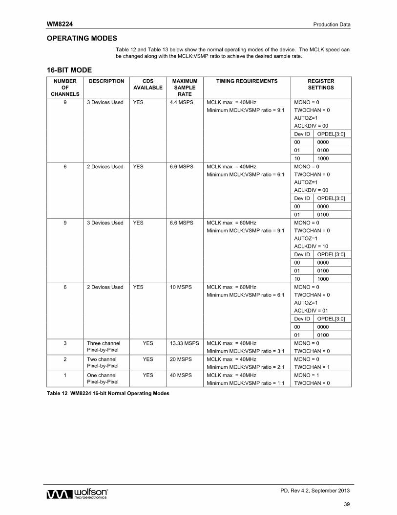
OPERATING MODES
Table 12 and Table 13 below show the normal operating modes of the device. The MCLK speed can be changed along with the MCLK:VSMP ratio to achieve the desired sample rate.
16-BIT MODE
NUMBER OF
CHANNELS
DESCRIPTION CDS AVAILABLE
MAXIMUM SAMPLE
RATE
TIMING REQUIREMENTS REGISTER SETTINGS
9 3 Devices Used YES 4.4 MSPS MCLK max = 40MHz
Minimum MCLK:VSMP ratio = 9:1
MONO = 0
TWOCHAN = 0
AUTOZ=1
ACLKDIV = 00
Dev ID OPDEL[3:0]
00 0000
01 0100
10 1000
6 2 Devices Used YES 6.6 MSPS MCLK max = 40MHz
Minimum MCLK:VSMP ratio = 6:1
MONO = 0
TWOCHAN = 0
AUTOZ=1
ACLKDIV = 00
Dev ID OPDEL[3:0]
00 0000
01 0100
9 3 Devices Used YES 6.6 MSPS MCLK max = 60MHz
Minimum MCLK:VSMP ratio = 9:1
MONO = 0
TWOCHAN = 0
AUTOZ=1
ACLKDIV = 10
Dev ID OPDEL[3:0]
00 0000
01 0100
10 1000
6 2 Devices Used YES 10 MSPS MCLK max = 60MHz
Minimum MCLK:VSMP ratio = 6:1
MONO = 0
TWOCHAN = 0
AUTOZ=1
ACLKDIV = 01
Dev ID OPDEL[3:0]
00 0000
01 0100
3 Three channel Pixel-by-Pixel
YES 13.33 MSPS MCLK max = 40MHz
Minimum MCLK:VSMP ratio = 3:1
MONO = 0
TWOCHAN = 0
2 Two channel Pixel-by-Pixel
YES 20 MSPS MCLK max = 40MHz
Minimum MCLK:VSMP ratio = 2:1
MONO = 0
TWOCHAN = 1
1 One channel Pixel-by-Pixel
YES 40 MSPS MCLK max = 40MHz
Minimum MCLK:VSMP ratio = 1:1
MONO = 1
TWOCHAN = 0
Table 12 WM8224 16-bit Normal Operating Modes

WM8224 Production Data
w PD, Rev 4.2, September 2013
40
10-BIT MODE
NUMBER OF
CHANNELS
DESCRIPTION CDS AVAILABLE
MAXIMUM SAMPLE
RATE
TIMING REQUIREMENTS REGISTER SETTINGS
9 3 Devices Used YES 6.6 MSPS MCLK max = 60MHz
Minimum MCLK:VSMP ratio = 9:1
MONO = 0
TWOCHAN = 0
AUTOZ=1
Dev ID OPDEL[3:0]
00 0000
01 0100
10 1000
6 2 Devices Used YES 10 MSPS MCLK max = 60MHz
Minimum MCLK:VSMP ratio = 6:1
MONO = 0
TWOCHAN = 0
AUTOZ=1
Dev ID OPDEL[3:0]
00 0000
01 0100
3 Three channel Pixel-by-Pixel
YES 20 MSPS MCLK max = 60MHz
Minimum MCLK:VSMP ratio = 3:1
MONO = 0
TWOCHAN = 0
2 Two channel Pixel-by-Pixel
YES 30 MSPS MCLK max = 60MHz
Minimum MCLK:VSMP ratio = 2:1
MONO = 0
TWOCHAN = 1
1 One channel Pixel-by-Pixel
YES 60 MSPS MCLK max = 60MHz
Minimum MCLK:VSMP ratio = 1:1
MONO = 1
TWOCHAN = 0
Table 13 WM8224 10-bit Normal Operating Modes
Table 14 below shows the different channel mode register settings required to operate the 8224 in 1, 2 and 3 channel modes.
MONO TWOCHAN CHAN[1:0] MODE DESCRIPTION
0 0 XX 3-channel (colour mode)
0 1 00 2-channel mode
Green and Blue channels selected, Red PGA disabled
0 1 01 2-channel mode
Red and Blue channels selected, Green PGA disabled
0 1 10 2-channel mode
Red & Green channels selected, Blue PGA disabled
1 0 00 1-channel (monochrome) mode.
Red channel selected, Green and Blue PGAs disabled.
1 0 01 1-channel (monochrome) mode.
Green channel selected, Red and Blue PGAs disabled.
1 0 10 1-channel (monochrome) mode.
Blue channel selected, Red and Green PGAs disabled.
X X 11 Invalid mode
1 1 XX Invalid mode
Table 14 Sampling Mode Summary
Note: Unused input pins should be connected to AGND unless reset level clamping is used.

WM8224 Production Data
w PD, Rev 4.2, September 2013
41
DEVICE CONFIGURATION
REGISTER MAP
The following table describes the location of each control bit used to determine the operation of the WM8224.
ADDRESS
<a5:a0>
DESCRIPTION DEF
(hex)
RW
BIT
b7 b6 b5 b4 b3 b2 b1 b0
000000 (00h) Device ID 82 R Reads first 2 digits of device part number
000001 (01h) Setup Reg 1 03 RW ACLKDIV[1] ACLKDIV[0] PGAFS[1] PGAFS[0] TWOCHAN MONO CDS EN
000010 (02h) Setup Reg 2 E8 RW RES[1] RES[0] RLCDACRNG LOWREFS OPD INVOP AUTOZ OPFORM
000011 (03h) Setup Reg 3 1F RW CHAN[1] CHAN[0] OEDEL[1] OEDEL[0] RLCDAC[3] RLCDAC[2] RLCDAC[1] RLCCDAC[0]
000100 (04h) Software Reset 24 RW Reads second 2 digits of device part number
000101 (05h) Device ID Revision 01 R Reads revision number of device
000110 (06h) Setup Reg 4 00 RW OPDEL[3] OPDEL[2] OPDEL[1] OPDEL[0] 0 0 0 0
000111 (07h) Setup Reg 5 00 RW 0 0 ADCREFPD VRLCDACPD ADCPD BLUPD GRNPD REDPD
001000 (08h) Setup Reg 6 20 RW FOL_EN CLAMPCTRL RLCEN 0 0 0 0 RESET_NOREG
001001 (09h) BLC Red Target 00 RW TARGETR[7] TARGETR[6] TARGETR[5] TARGETR[4] TARGETR[3] TARGETR[2] TARGETR[1] TARGETR[0]
001010 (0Ah) BLC Green Target 00 RW TARGETG[7] TARGETG[6] TARGETG[5] TARGETG[4] TARGETG[3] TARGETG[2] TARGETG[1] TARGETG[0]
001011 (0Bh) BLC Blue Target 00 RW TARGETB[7] TARGETB[6] TARGETB[5] TARGETB[4] TARGETB[3] TARGETB[2] TARGETB[1] TARGETB[0]
001100 (0Ch) BLC Control 1 00 RW STATE_OUT 0 0 0 FSCALE_REL
TG_REG TG_METHOD
[1] TG_METHOD
[0]
001101 (0Dh) BLC Control 2 00 RW 0 0 0 0 FA_EN CADUR[2] CADUR[1] CADUR[0]
001110 (0Eh) BLC Control 3 00 RW BPIX_AVAIL [9]
BPIX_AVAIL [8]
CA_ EVERYLINE
FA_ EVERYLINE
FA_ACCUM FRAME_SEQ SEQ_START FRAME_ START
001111 (Ofh) BLC Control 4 00 RW BPIX_AVAIL [7]
BPIX_AVAIL [6]
BPIX_AVAIL [5]
BPIX_AVAIL [4]
BPIX_AVAIL [3]
BPIX_AVAIL [2]
BPIX_AVAIL [1]
BPIX_AVAIL [0]
100000 (20h) DAC Value (Red) 80 RW DACR[7] DACR[6] DACR[5] DACR[4] DACR[3] DACR[2] DACR[1] DACR[0]
100001 (21h) DAC Value (Green) 80 RW DACG[7] DACG[6] DACG[5] DACG[4] DACG[3] DACG[2] DACG[1] DACG[0]
100010 (22h) DAC Value (Blue) 80 RW DACB[7] DACB[6] DACB[5] DACB[4] DACB[3] DACB[2] DACB[1] DACB[0]
100011 (23h) DAC Value (RGB) 80 W DACRGB[7] DACRGB[6] DACRGB[5] DACRGB[4] DACRGB[3] DACRGB[2] DACRGB[1] DACRGB[0]
100100 (24h) PGA Gain LSB (Red) 00 RW 0 0 0 0 0 0 0 PGAR[0]
100101 (25h) PGA Gain LSB (Green) 00 RW 0 0 0 0 0 0 0 PGAG[0]
100110 (26h) PGA Gain LSB (Blue) 00 RW 0 0 0 0 0 0 0 PGAB[0]
100111 (27h) PGA Gain LSB (RGB) 00 W 0 0 0 0 0 0 0 PGARGB[0]
101000 (28h) PGA Gain MSBs (Red) 0C RW PGAR[8] PGAR[7] PGAR[6] PGAR[5] PGAR[4] PGAR[3] PGAR[2] PGAR[1]
101001 (29h) PGA Gain MSBs (Green) 0C RW PGAG[8] PGAG[7] PGAG[6] PGAG[5] PGAG[4] PGAG[3] PGAG[2] PGAG[1]
101010 (2Ah) PGA Gain MSBs (Blue) 0C RW PGAB[8] PGAB[7] PGAB[6] PGAB[5] PGAB[4] PGAB[3] PGAB[2] PGAB[1]
101011 (2Bh) PGA Gain MSBs (RGB) 0C W PGARGB[8] PGARGB[7] PGARGB[6] PGARGB[5] PGARGB[4] PGARGB[3] PGARGB[2] PGARGB[1]
101100(2Ch) BLC Control 5 00 RW LINE_DEL[8] BLC_DEL[6] BLC_DEL[5] BLC_DEL[4] BLC_DEL[3] BLC_DEL[2] BLC_DEL[1] BLC_DEL[0]
101101(2Dh) BLC Control 6 00 RW LINE_DEL[7] LINE_DEL[6] LINE_DEL[5] LINE_DEL[4] LINE_DEL[3] LINE_DEL[2] LINE_DEL[1] LINE_DEL[0]
Table 15 Register Map

WM8224 Production Data
w PD, Rev 4.2, September 2013
42
REGISTER MAP DESCRIPTION
The following table describes the function of each of the control bits shown in Table 15.
REGISTER REGISTER NAME
BIT NO
BIT NAME(S)
DEFAULT DESCRIPTION
R0 (00h) Device ID 7:0 10000010 Read only register. Reading from this register returns the first 2 digits of device part number.
R1 (01h) Setup Register 1
0 EN 1 Global Enable
0 = complete power down,
1 = fully active (individual blocks can be disabled using individual powerdown bits – see setup register 5).
1 CDS 1 Select correlated double sampling mode:
0 = non-CDS mode, 1 = CDS mode.
2 MONO 0 Sampling mode select
0 = other mode (2 or 3-channel)
1 = Monochrome (1-channel) mode. Input channel selected by CHAN[1:0] register bits, unused channel is powered down.
TWOCHAN and MONO should not be set concurrently.
3 TWOCHAN 0 Sampling mode select
0 = other mode (1 or 3-channel)
1 = 2-channel mode.
TWOCHAN and MONO should not be set concurrently.
5:4 PGAFS[1:0] 00 Offsets PGA output to optimise the ADC range for different polarity sensor output signals. Zero differential PGA input signal gives:
0x = Zero output from the PGA (Output code=511)
10 = Full-scale positive output (OP=1023) – use for negative going video.
NB, Set INVOP=1 if zero differential input should give a zero output code with negative going video.
11 = Full-scale negative output (OP=0) - use for positive going video
7:6 ACLKDIV[1:0] 00 Reduces the internal clock frequency to allow analogue circuitry to run at a slower rate when daisy chaining devices.
00 – no divide
01 – divide MCLK by 2 internally
10 – divide MCLK by 3 internally
11 – not valid

WM8224 Production Data
w PD, Rev 4.2, September 2013
43
REGISTER REGISTER NAME
BIT NO
BIT NAME(S)
DEFAULT DESCRIPTION
R2 (02h) Setup Register 2
0 OPFORM 0 Output format :
0 = Multiplexed mode
1 = Parallel mode
1 AUTOZ 0 When set the output goes to high impedance other than during valid data output. This will override the OEB/OPD control.
0 = Output pins high impedance mode controlled by OPD/OEB
1 = Output pins high impedance mode controlled automatically. Normally used in multiple device mode where several devices share a common data bus.
AUTOZ should not be set if MCLK:VSMP is 1:1.
2 INVOP 0 Digitally inverts the polarity of output data.
0 = negative going video gives negative going output, 1 = negative-going video gives positive going output data.
3 OPD 1 Output Disable. This works with the OEB pin to control the output pins.
This is only valid if AUTOZ=0.
0=Digital outputs enabled, 1=Digital outputs high impedance
OEB (pin) OPD OP pins
0 0 Enabled
0 1 High Impedance
1 0 High Impedance
1 1 High impedance
4 LOWREFS 0 Reduces the ADC reference range (2*[VRT-VRB]), thus
changing the max/min input video voltages (ADC ref
range/PGA gain).
0= ADC reference range = 2.0V 1= ADC reference range = 1.2V
5 RLCDACRNG 1 Sets the output range of the RLCDAC.
0 = RLCDAC ranges from 0 to AVDD (approximately), 1 = RLCDAC ranges from 0 to VRT (approximately).
7:6 RES[1:0] 11 Controls the device output resolution:
RES Output Resolution
00 8-bit
01 10-bit
10 12-bit
11 16-bit
R3 (03h) Setup Register 3
3:0 RLCDAC[3:0] 1111 Controls RLCDAC driving VRLC/VBIAS pin to define single ended signal reference voltage or Reset Level Clamp voltage. See Electrical Characteristics section for ranges.
5:4 OEDEL[1:0] 01 Adjustable delay for beginning of automatic OE signal.
Only valid when AUTOZ=1
00 : typically adds 0.5ns to tPD time
01 : typically adds 1.0ns to tPD time
10 : typically adds 1.5ns to tPD time
11 : typically adds 2.0ns to tPD time
7:6 CHAN[1:0] 00 When MONO=0 and TWOCHAN=0 this register bit has no effect
When MONO=1:
00 = Red channel select 01 = Green channel select
10 = Blue channel select 11 = Reserved

WM8224 Production Data
w PD, Rev 4.2, September 2013
44
REGISTER REGISTER NAME
BIT NO
BIT NAME(S)
DEFAULT DESCRIPTION
When TWOCHAN=1: 00 = Red PGA disabled (G&B only) 01 = Green PGA disabled (R&B only)
10 = Blue PGA disabled (R&G only) 11 = Reserved
R4 (04h) Software Reset
7:0 00100100 Any write to Software Reset causes all register bits to be reset. It is recommended that a software reset be performed after a power-up before any other register writes.
Reading from this register returns the last 2 digits of the device part number.
R5 (05h) Device ID Revision
7:0 00000001 Reading from this register returns the revision number of the device.
R6 (06h) Setup Register 4
3:0 Reserved 0000 Must be set to 0000
7:4 OPDEL[3:0] 000 Output latency adjust (ACLKDIV=00).
0000 = Minimum latency (7 MCLK periods)
0001 = 8 MCLK periods
0010 = 9 MCLK periods
0011 = 10 MCLK periods
0100 = 11 MCLK periods
0101 = 12 MCLK periods
0110 = 13 MCLK periods
0111 = 14 MCLK periods
1000 = 15 MCLK periods
1001 to 1111 = Invalid settings
R7 (07h) Setup Register 5
0 REDPD 0 When set powers down red S/H, PGA
1 GRNPD 0 When set powers down green S/H, PGA
2 BLUPD 0 When set powers down blue S/H, PGA
3 ADCPD 0 When set powers down ADC. Allows reduced power
consumption without powering down the references which
have a long time constant when switching on/off due to the
external decoupling capacitors.
4 VRLCDACPD
0 When set powers down 4-bit RLCDAC, setting the output
to a high impedance state and allowing an external
reference to be driven in on the VRLC/VBIAS pin.
5 ADCREFPD 0 When set disables VRT, VRB buffers to allow external
references to be used.
7:6 Reserved 00 Must be set to 00
R8 (08h) Setup Register 6
0 RESET_NO
REG
0 When set reset the digital clocking without register reset.
4:1 Reserved 0000 Must be set to 0
5 RLCEN 1 Reset Level Clamp Enable. When set Reset Level Clamping is enabled. The method of clamping is determined by CLAMPCTRL.
6 CLAMPCTRL 0 0 = RLC switch is controlled directly from RSMP input pin:
RSMP = 0: switch is open
RMSP = 1: switch is closed
1 = RLC switch is controlled by logical combination of
RSMP and VSMP. RSMP && VSMP = 0: switch is open
Switch is re-opened when:
VSMP=0 (non-CDS mode)
VSMP=0 and RSMP=0 (CDS mode)
7 FOL_EN 0 Enables internal input voltage buffers, to minimise code
drift if not pixel clamping, when using an ac coupling
capacitor in non-CDS mode (CDS=0).
Line clamping should be used when this bit is set.

WM8224 Production Data
w PD, Rev 4.2, September 2013
45
REGISTER REGISTER NAME
BIT NO
BIT NAME(S)
DEFAULT DESCRIPTION
R9 (09h) BLC Red Target
7:0 TARGETR [7:0]
00000000 Target Black-Level code for Red channel. Please see the
Target Codes Section for details.
R10 (0Ah) BLC Green Target
7:0 TARGETG [7:0]
00000000 Target Black-Level code for Green channel. Please see
the Target Codes Section for details.
R11 (0Bh) BLC Blue Target
7:2 TARGETB [7:0]
00000000 Target Black-Level code for Blue channel. Please see the
Target Codes Section for details.
R12 (0Ch) BLC Control 1
1:0 TG_METHOD
[1:0]
00 Determines the start-of-line method to be used.
00 = TG_REG method
01 = Not a valid option
10 = OEB/TG shared pin method, +ve edge triggered
11 = OEB/TG shared pin method, -ve edge triggered
2 TG_REG 0 Register flag to indicate a start-of-line, this register is
automatically set to zero after it has been clocked by the
BLC.
3 FSCALE_ REL
0 Inverts the Black-level target codes so they are relative to
fullscale.
4 RESERVED 0 Set to zero
6:5 RESERVED 00 Set to zero
7 STATE_OUT 0 Outputs the 2-bit state of the BLC onto OP0 and OP1.
R13 (0Dh) BLC Control 2
2:0 CADUR[2:0] 000 Controls the number of Coarse Adjust iterations to be
performed.
3 FA_EN 0 Enables the Fine Adjust operation
7:4 RESERVED 0000 Set to zero
R14 (0Eh) BLC Control 3
0 FRAME_ START
0 Register to indicate that the next start-of-line indicator is
the first line in a frame. This register is automatically set
to zero at the end of the BLC operation on the first line.
1 SEQ_START 0 Register to indicate that the next start-of-line indicator is
the first line of the first frame in a frame-sequence. This
register is automatically set to zero at the end of the BLC
operation on the first line.
2 FRAME_SEQ 0 Indicates that the BLC is to be used in a sequence of
frames
3 FA_ACCUM 0 Makes the Fine Adjust calibration accumulate a result over
multiple lines.
4 FA_ EVERYLINE
0 0 = Fine Adjust only used on the 1st line of a frame
1 = Fine Adjust used on every line of a frame
5 CA_ EVERYLINE
0 0 = Coarse Adjust only used on the 1st line of a frame
1 = Coarse Adjust used on every line of a frame
7:6 BPIX_AVAIL [9:8]
00 MSBs of the number of Black-pixels available over which
to perform the Coarse and/or Fine Adjust Calibration.
R15 (0Fh) BLC Control 4
7:0 BPIX_AVAIL [7:0]
00000000 LSBs of the number of Black-pixels available over which to
perform the Coarse and/or Fine Adjust Calibration.
R32 (20h) Offset DAC (Red)
7:0 DACR[7:0] 10000000 Red channel 8-bit offset DAC value (mV) = 250*(DACR[7:0]-127.5)/127.5
R33 (21h) Offset DAC (Green)
7:0 DACG[7:0] 10000000 Green channel 8-bit offset DAC value (mV) = 250*(DACG[7:0]-127.5)/127.5
R34 (22h) Offset DAC (Blue)
7:0 DACB[7:0] 10000000 Blue channel 8-bit offset DAC value (mV) = 250*(DACB[7:0]-127.5)/127.5
R35 (23h) Offset DAC
(RGB)
7:0 DACRGB[7:0] - A write to this register location causes the red, green and blue offset DAC registers to be overwritten by the new value
R36 (24h) PGA Gain
LSB
(Red)
0 PGAR[0] 0 This register bit forms the LSB of the red channel PGA gain code. PGA gain is determined by combining this register bit and the 8 MSBs contained in register address 28 hex.

WM8224 Production Data
w PD, Rev 4.2, September 2013
46
REGISTER REGISTER NAME
BIT NO
BIT NAME(S)
DEFAULT DESCRIPTION
R37 (25h) PGA Gain
LSB
(Green)
0 PGAG[0] 0 This register bit forms the LSB of the green channel PGA gain code. PGA gain is determined by combining this register bit and the 8 MSBs contained in register address 29 hex.
R38 (26h) PGA Gain
LSB
(Blue)
0 PGAB[0] 0 This register bit forms the LSB of the blue channel PGA
gain code. PGA gain is determined by combining this
register bit and the 8 MSBs contained in register address
2A hex.
R39 (27h) PGA Gain
LSB
(RGB)
0 PGARGB[0] - Writing a value to this location causes red, green and blue
PGA LSB gain values to be overwritten by the new value.
R40 (28h) PGA gain MSBs
(Red)
7:0 PGAR[8:1] 00001100 Bits 8 to 1 of red PGA gain. Combined with red LSB register bit to form complete PGA gain code. This determines the gain of the red channel PGA according to the equation:
Red channel PGA gain (V/V) = 0.66 + PGAR[8:0]x7.34/511
R41 (29h) PGA gain MSBs (Green)
7:0 PGAG[8:1] 00001100 Bits 8 to 1 of green PGA gain. Combined with green LSB register bit to form complete PGA gain code. This determines the gain of the green channel PGA according to the equation:
Green channel PGA gain (V/V) = 0.66 + PGAG[8:0]x7.34/511
R42 (2Ah) PGA gain MSBs
(Blue)
7:0 PGAB[8:1] 00001100 Bits 8 to 1 of blue PGA gain. Combined with blue LSB register bit to form complete PGA gain code. This determines the gain of the blue channel PGA according to the equation:
Blue channel PGA gain (V/V) = 0.66 + PGAB[8:0]x7.34/511
R43 (2Bh) PGA gain MSBs
(RGB)
7:0 PGARGB[8:1] - A write to this register location causes the red, green and blue PGA MSB gain registers to be overwritten by the new value.
R44 (2Ch) BLC Control 5
6:0 BLC_DEL
[6:0]
0000000 Determines the number of pixels (from the start of a line) to delay the start of a BLC operation.
7 LINE_DEL
[8]
0 MSB of the number of lines from the start of a frame to delay the start of a BLC operation.
R45 (2Dh) BLC Control 6
7:0 LINE_DEL
[7:0]
00000000 LSBs of the number of lines from the start of a frame to delay the start of a BLC operation.
Table 16 Register Control Bits

WM8224 Production Data
w PD, Rev 4.2, September 2013
47
APPLICATIONS INFORMATION
RECOMMENDED EXTERNAL COMPONENTS
Figure 39 External Components Diagram
RECOMMENDED EXTERNAL COMPONENT VALUES
COMPONENT REFERENCE
SUGGESTED VALUE
DESCRIPTION
C1 100nF De-coupling for DVDD
C2 100nF De-coupling for AVDD
C3 1F Ceramic de-coupling between VRT and VRB (non polarized)
C4 100nF De-coupling for VRB
C5 100nF De-coupling for VRX
C6 100nF De-coupling for VRT
C7 100nF De-coupling for VRLC
C8 10F Reservoir capacitor for DVDD
C9 10F Reservoir capacitor for AVDD
Table 17 External Components Descriptions

WM8224 Production Data
w PD, Rev 4.2, September 2013
48
PACKAGE DIMENSIONS
DM101.AFL: 32 PIN QFN PLASTIC PACKAGE 5 X 5 X 0.9 mm BODY, 0.50 mm LEAD PITCH
E2
bB
16 15
8
9
e
C0.08
Cccc
A
A1C
A3
SEATING PLANE
1
L
INDEX AREA(D/2 X E/2)
TOP VIEW
D
Caaa2 X
Caaa2 X
E
1
17
24
25 32
D2
BCbbb M A
5
4
NOTES:1. DIMENSION b APPLIES TO METALLIZED TERMINAL AND IS MEASURED BETWEEN 0.15 mm AND 0.30 mm FROM TERMINAL TIP. 2. FALLS WITHIN JEDEC, MO-220, VARIATION VHHD-5. 3. ALL DIMENSIONS ARE IN MILLIMETRES.4. THE TERMINAL #1 IDENTIFIER AND TERMINAL NUMBERING CONVENTION SHALL CONFORM TO JEDEC 95-1 SPP-002.5. COPLANARITY APPLIES TO THE EXPOSED HEAT SINK SLUG AS WELL AS THE TERMINALS.6. REFER TO APPLICATION NOTE WAN_0118 FOR FURTHER INFORMATION REGARDING PCB FOOTPRINTS AND QFN PACKAGE SOLDERING.7. THIS DRAWING IS SUBJECT TO CHANGE WITHOUT NOTICE.
DETAIL 1
A3G
T
H
W
b
Exposed lead
Half etch tie bar
Dimensions (mm)Symbols
MIN NOM MAX NOTE
A
A1
A3
0.80 0.90 1.00
0.050.0200.203 REF
b
D
D2
EE2
e
L
0.300.18
5.00 BSC3.603.453.30
0.50 BSC
0.30 0.40 0.50
1
2
25.00 BSC
3.603.453.30
0.10
aaa
bbbccc
REF:
0.15
0.10
JEDEC, MO-220, VARIATION VHHD-5.
Tolerances of Form and Position
0.25
H 0.1
0.20G
T 0.103
W 0.15
DETAIL 1
DETAIL 2
DETAIL 2
EXPOSEDGROUND PADDLE
6
EXPOSED GROUNDPADDLE
BOTTOM VIEW
SIDE VIEW
0.30
45°M M

WM8224 Production Data
w PD, Rev 4.2, September 2013
49
IMPORTANT NOTICE
Wolfson Microelectronics plc (“Wolfson”) products and services are sold subject to Wolfson’s terms and conditions of sale, delivery and payment supplied at the time of order acknowledgement.
Wolfson warrants performance of its products to the specifications in effect at the date of shipment. Wolfson reserves the right to make changes to its products and specifications or to discontinue any product or service without notice. Customers should therefore obtain the latest version of relevant information from Wolfson to verify that the information is current.
Testing and other quality control techniques are utilised to the extent Wolfson deems necessary to support its warranty. Specific testing of all parameters of each device is not necessarily performed unless required by law or regulation.
In order to minimise risks associated with customer applications, the customer must use adequate design and operating safeguards to minimise inherent or procedural hazards. Wolfson is not liable for applications assistance or customer product design. The customer is solely responsible for its selection and use of Wolfson products. Wolfson is not liable for such selection or use nor for use of any circuitry other than circuitry entirely embodied in a Wolfson product.
Wolfson’s products are not intended for use in life support systems, appliances, nuclear systems or systems where malfunction can reasonably be expected to result in personal injury, death or severe property or environmental damage. Any use of products by the customer for such purposes is at the customer’s own risk.
Wolfson does not grant any licence (express or implied) under any patent right, copyright, mask work right or other intellectual property right of Wolfson covering or relating to any combination, machine, or process in which its products or services might be or are used. Any provision or publication of any third party’s products or services does not constitute Wolfson’s approval, licence, warranty or endorsement thereof. Any third party trade marks contained in this document belong to the respective third party owner.
Reproduction of information from Wolfson datasheets is permissible only if reproduction is without alteration and is accompanied by all associated copyright, proprietary and other notices (including this notice) and conditions. Wolfson is not liable for any unauthorised alteration of such information or for any reliance placed thereon.
Any representations made, warranties given, and/or liabilities accepted by any person which differ from those contained in this datasheet or in Wolfson’s standard terms and conditions of sale, delivery and payment are made, given and/or accepted at that person’s own risk. Wolfson is not liable for any such representations, warranties or liabilities or for any reliance placed thereon by any person.
ADDRESS:
Wolfson Microelectronics plc
Westfield House
26 Westfield Road
Edinburgh
EH11 2QB
Tel :: +44 (0)131 272 7000
Fax :: +44 (0)131 272 7001
Email :: [email protected]

WM8224 Production Data
w PD, Rev 4.2, September 2013
50
REVISION HISTORY
DATE REV ORIGINATOR CHANGES
15/05/12 4.1 JMacD Order codes updated from WM8224SEFL and WM8224SEFL/R to WM8224CSEFL and WM8224CSEFL/R to reflect change to copper wire bonding.
15/05/12 4.1 JMacD Package Diagram updated to DM101.A
23/09/13 4.2 A.A Updated the note of POWER MANAGEMENT section
Updated the REGISTER MAP. (Added RESET_NOREG register in Setup Reg 6)