6 W bias supply - docs.rs-online.com
20
Application Note Please read the Important Notice and Warnings at the end of this document Revision 1.0 www.infineon.com/p7 20.07.2018 AN_1801_PL52_1803_160336 6 W bias supply Using the new 950 V CoolMOS™ P7, ICE5QSAG QR flyback controller, and snubberless flyback for improved auxiliary power supply efficiency and form-factor Order code: KIT_6W_12V_P7_950V Author: Jared Huntington Stefan Preimel Scope and purpose In power supplies that are used for server, telecom and industrial applications there is typically a small bias power supply in addition to the main power converter. This bias supply is used to power the fan, controllers, and any additional monitoring and control logic on the board. This application note gives an overview of a bias supply designed for the Infineon high-power demo boards. This bias board is designed to run in a system where it is continuously powered from the 400 V DC output of a boost Power Factor Correction (PFC) converter. This board uses the ICE5QSAG Quasi Resonant (QR) flyback controller and a 950 V CoolMOS™ P7 (IPU95R3K7P7), from the latest generation of devices. This design was done as a snubberless flyback converter to further improve efficiency. These new Infineon devices and the snubberless operation give a 9.6 percent efficiency improvement with a 6 W load and a 27.0 percent improvement with a 1 W load compared to the previous bias board using 800 V CoolMOS™ C3 technology. The form factor was also improved to increase the system level power density. This document contains an overview of the design decisions, an overview of the snubberless operation, performance benchmarking, and guidance on how to adapt this board for other applications. Intended audience Power supply design engineers Table of contents 1 Overview and key results................................................................................................ 2 2 Design changes overview ................................................................................................ 4 2.1 Transitioning from 800 V CoolMOS™ C3 to 950 V CoolMOS™ P7 ......................................................... 4 2.2 ICE5QSAG – QR flyback controller .......................................................................................................... 4 2.3 Snubber network..................................................................................................................................... 5 2.4 Transformer ............................................................................................................................................. 5 2.5 Output capacitors ................................................................................................................................... 6 3 Snubberless flyback design ............................................................................................. 7 4 Possible design changes ................................................................................................ 11 4.1 Lowering the cost .................................................................................................................................. 11 5 Demo board overview ................................................................................................... 12 5.1 Demo board pictures............................................................................................................................. 12 5.2 Demo board specifications ................................................................................................................... 12 5.3 Schematic .............................................................................................................................................. 13 5.4 PCB layout ............................................................................................................................................. 14 5.5 Transformer construction ..................................................................................................................... 14 5.6 Bill of Materials (BOM) ........................................................................................................................... 15 6 Conclusion ................................................................................................................... 17 7 References ................................................................................................................... 18 Revision history............................................................................................................................. 19
Transcript of 6 W bias supply - docs.rs-online.com

Application Note Please read the Important Notice and Warnings at the end of this document Revision 1.0
www.infineon.com/p7 20.07.2018
AN_1801_PL52_1803_160336
6 W bias supply
Using the new 950 V CoolMOS™ P7, ICE5QSAG QR flyback controller, and snubberless flyback for improved
auxiliary power supply efficiency and form-factor
Order code: KIT_6W_12V_P7_950V
Author: Jared Huntington
Stefan Preimel
Scope and purpose
In power supplies that are used for server, telecom and industrial applications there is typically a small bias
power supply in addition to the main power converter. This bias supply is used to power the fan, controllers, and
any additional monitoring and control logic on the board. This application note gives an overview of a bias supply designed for the Infineon high-power demo boards. This bias board is designed to run in a system where it is continuously powered from the 400 V DC output of a boost Power Factor Correction (PFC) converter. This
board uses the ICE5QSAG Quasi Resonant (QR) flyback controller and a 950 V CoolMOS™ P7 (IPU95R3K7P7),
from the latest generation of devices. This design was done as a snubberless flyback converter to further improve efficiency. These new Infineon devices and the snubberless operation give a 9.6 percent efficiency
improvement with a 6 W load and a 27.0 percent improvement with a 1 W load compared to the previous bias board using 800 V CoolMOS™ C3 technology. The form factor was also improved to increase the system level
power density. This document contains an overview of the design decisions, an overview of the snubberless operation, performance benchmarking, and guidance on how to adapt this board for other applications.
Intended audience
Power supply design engineers
Table of contents
1 Overview and key results ................................................................................................ 2
2 Design changes overview ................................................................................................ 4
2.1 Transitioning from 800 V CoolMOS™ C3 to 950 V CoolMOS™ P7 ......................................................... 4 2.2 ICE5QSAG – QR flyback controller .......................................................................................................... 4
2.3 Snubber network ..................................................................................................................................... 5 2.4 Transformer ............................................................................................................................................. 5
2.5 Output capacitors ................................................................................................................................... 6
3 Snubberless flyback design ............................................................................................. 7
4 Possible design changes ................................................................................................ 11 4.1 Lowering the cost .................................................................................................................................. 11
5 Demo board overview ................................................................................................... 12
5.1 Demo board pictures ............................................................................................................................. 12 5.2 Demo board specifications ................................................................................................................... 12 5.3 Schematic .............................................................................................................................................. 13 5.4 PCB layout ............................................................................................................................................. 14
5.5 Transformer construction ..................................................................................................................... 14
5.6 Bill of Materials (BOM) ........................................................................................................................... 15
6 Conclusion ................................................................................................................... 17
7 References ................................................................................................................... 18
Revision history............................................................................................................................. 19

Application Note 2 Revision 1.0
20.07.2018
6 W bias supply Using the new 950 V CoolMOS™ P7, ICE5QSAG QR flyback controller, and snubberless
flyback for improved auxiliary power supply efficiency and form-factor
Overview and key results
1 Overview and key results
In high-power supplies that are used for server, telecom and industrial applications, there is typically a small bias power supply in addition to the main power converter. This small bias supply powers the gate drivers,
controllers, fans and any additional small signal devices on the PCB. This controls the power-up sequence of the different sections of the power supply. A separate bias supply also ensures that monitoring and control circuitry will continue to run through fault conditions on the main supply. This bias power supply begins to play a larger role in the system losses at light load and under standby conditions.
This 6 W bias board was designed as a replacement for an existing bias board used in high-power Infineon demo boards. The goal was to be pin-to-pin compatible with the previous bias supply design, but to also improve the efficiency and form factor, allowing for higher system level power density. The previous bias board
used the CoolMOS™ C3 technology, and this provided an opportunity to update the board with the latest Infineon devices. The board has a 12 V output that is regulated on the primary side, and the secondary is an unregulated 12 V output. It is designed to provide 6 W of operation from 120 V DC to 440 V DC.
Figure 1 The picture on the left shows a 6 W bias board used in the Infineon 2 kW ZVS full-bridge demo
board, and the block diagram on the right shows a typical configuration

Application Note 3 Revision 1.0
20.07.2018
6 W bias supply Using the new 950 V CoolMOS™ P7, ICE5QSAG QR flyback controller, and snubberless
flyback for improved auxiliary power supply efficiency and form-factor
Overview and key results
The performance of the new design (with 950 V CoolMOS™ P7) compared to the old version (with 800 V CoolMOS™ C3) can be seen in Figure 2. The efficiency improvement is between 9.6 percent and 27.0 percent over the 1 W to 6 W load range, shown by the red line. The underside of the new bias board can be seen, along
with the reduction in the overall form factor. It can also be seen that by changing from 800 V CoolMOS™ P7 to 950 V CoolMOS™ P7 there is an efficiency gain by reducing the VDS capacitor for snubberless operation from 100
pF to 10 pF, which helps to reduce the overall switching losses of the system. The 950 V CoolMOS™ P7 also helps to increase the MOSFET breakdown voltage margin of the design to 20.6 percent margin.
Figure 2 The improvement in efficiency at 400 V DC and the form factor
+9.6
percent
-876 mW
+27
percent

Application Note 4 Revision 1.0
20.07.2018
6 W bias supply Using the new 950 V CoolMOS™ P7, ICE5QSAG QR flyback controller, and
snubberless flyback for improved auxiliary power supply efficiency and form-
factor Design changes overview
2 Design changes overview
2.1 Transitioning from 800 V CoolMOS™ C3 to 950 V CoolMOS™ P7
Figure 3 950 V CoolMOS™ P7 compared to the closest performing competitor in the 6 W bias board
The original bias board used the third-generation CoolSET™, which uses the C3 MOSFET technology. Switching
to the latest CoolMOS™ P7 brings performance benefits. The gate driving losses of the device are lower, and the
RDS(on) change vs temperature is lower than the previous generation of devices. The P7 also has lower output
capacitance energy storage vs voltage, but in this design some of these benefits are reduced by the additional
CDS capacitor that needs to be added for the snubberless operation, as stated below. The efficiency compared to
the closest equivalent competitor part is shown in Figure 3, which shows a 1.4 percent efficiency gain at 1.2 W of output and a 0.4 percent efficiency gain at full load.
2.2 ICE5QSAG – QR flyback controller
Figure 4 Fixed-frequency flyback primary MOSFET drain source waveform (left) vs a QR flyback primary
MOSFET drain source waveform (right)
The design was switched from a fixed-frequency flyback controller to the new ICE5QSAG standalone QR flyback controller. The QR flyback helps to reduce the switching losses in the MOSFET by using the DCM resonant period
of the flyback and then only turning on the MOSFET in this valley.
-1,6%
-1,2%
-0,8%
-0,4%
0,0%
0,4%
0,0 1,0 2,0 3,0 4,0 5,0 6,0
Effi
cien
cy (
%)
Output Power (W)
Competitor vs. P7 950V
IPU95R3K7P7
Competitor
MOSFET Turn ON MOSFET Turn ON

Application Note 5 Revision 1.0
20.07.2018
6 W bias supply Using the new 950 V CoolMOS™ P7, ICE5QSAG QR flyback controller, and
snubberless flyback for improved auxiliary power supply efficiency and form-
factor Design changes overview
Since the turn-on switching losses are a function of V2 (as shown below), this reduces the overall system switching losses. This has the added benefit of lowering the amount of switched energy, which helps reduce switching noise from the converter, resulting in lower radiated and conducted emissions.
𝑃𝑠𝑤_𝑜𝑛 = 0.5𝑓𝑠𝑤𝐶𝑂𝑆𝑆𝑉𝐷𝑆2
2.3 Snubber network
Figure 5 Typical RCD snubber network (in red). In this design the snubber was removed to increase
efficiency.
The original bias board design was using an RCD snubber network. This network dissipates energy every
switching cycle regardless of the load, since the RCD capacitor is charged up to the reflected voltage of the secondary. By removing the snubber network and switching to a snubberless design, the overall efficiency was
improved. This was done using a MOSFET with a 950 V breakdown voltage, which also helps with the margin in snubberless operation. A 21 percent margin was kept from the drain source breakdown voltage to the peak drain
source voltage seen on the MOSFET during full load and maximum DC input voltage operation. An overview of the snubberless concept will be provided in the next section of the application note.
2.4 Transformer
Figure 6 The single-layer construction is shown on the left, while right is the new interleaved
transformer construction with a split primary winding to lower the leakage inductance

Application Note 6 Revision 1.0
20.07.2018
6 W bias supply Using the new 950 V CoolMOS™ P7, ICE5QSAG QR flyback controller, and
snubberless flyback for improved auxiliary power supply efficiency and form-
factor Design changes overview
The transformer design was changed from a single stacked design to an interleaved design. This can be seen in
Figure 6, above on the right, where the primary is split in half and stacked above and below the transformer stack-up. This helps to reduce the leakage inductance from the primary to the secondary, which affects the regulation of the secondary voltage since this is an unregulated winding. Reducing the leakage inductance is critical for the snubberless design of the system, because this additional leakage energy needs to be transferred
to the total CDS capacitance. This ends up determining the required CDS external ceramic capacitance, which has
an overall effect on the system efficiency.
2.5 Output capacitors
Figure 7 Output capacitors were changed to tantalum polymer capacitors for higher density
The capacitors were changed from 25 V electrolytic capacitors to 16 V tantalum polymer capacitors to reduce size. Since tantalum capacitors are a reliability concern when their rated voltage is exceeded, a 14 V Zener was
also added to the unregulated secondary rail to ensure that the secondary never goes beyond 14.5 V, even with
the primary fully loaded and the secondary unloaded. Under typical operating conditions there will be a load on the secondary side from the system, which will help to reduce the unregulated 12 V secondary voltage to avoid this over-voltage condition.

Application Note 7 Revision 1.0
20.07.2018
6 W bias supply Using the new 950 V CoolMOS™ P7, ICE5QSAG QR flyback controller, and
snubberless flyback for improved auxiliary power supply efficiency and form-
factor Snubberless flyback design
3 Snubberless flyback design
Figure 8 The typical RCD snubber configuration is shown on the left. The snubberless configuration
where this RCD network is removed is shown on the right.
The original bias board design was done using an RCD snubber network. By removing the snubber network and
switching to a snubberless design, the bias efficiency was improved. Switching losses and snubber losses play a large role in the losses of this supply due to the high-voltage operation with a 380 V DC nominal input voltage
and the fact that this is a low-power flyback where system conduction losses are minimal. In addition to
improving the system efficiency, the snubberless flyback converter also offers the benefits of reducing the
necessary PCB area and removing the cost of the RCD network.
Figure 9 Transitioning to a snubberless flyback reduces power losses by 439 mW (7.3 percent)
The losses of the system are reduced in a snubberless design due to removing two key loss mechanisms. The
first is that the RCD network charges up to the reflected voltage every switching cycle regardless of the system load. The leakage inductance energy also increases this voltage, leading to further losses across the snubber resistor. The second loss mechanism comes from the additional capacitance added to the switching node from the RCD network, as well as needing to charge the capacitance across the RCD diode junction. These loss mechanisms are eliminated by removing the RCD snubber network.
To keep the MOSFET drain source voltage from getting too high, an additional drain source capacitance is added
across the drain node of the MOSFET. This leads to a higher CDS switching loss when compared to the design with
0,0
0,1
0,2
0,3
0,4
0,5
0,6
0,7
0,8
RCD Snubber Snubberless
Psnubber R
P_SW_RCD
Pleakage
PCoss
+7.3 percent- 439 mW

Application Note 8 Revision 1.0
20.07.2018
6 W bias supply Using the new 950 V CoolMOS™ P7, ICE5QSAG QR flyback controller, and
snubberless flyback for improved auxiliary power supply efficiency and form-
factor Snubberless flyback design
a snubber network, as shown above in red. The energy that is stored in the transformer leakage inductance gets
dissipated in the high-frequency copper loss of the transformer rather than in the RCD network. The calculated efficiency improvement in this design from removing the snubber is 439 mW or around 7.3 percent at full load. These snubber losses are reduced throughout the output load range.
Figure 10 The MOSFET VDS margin must be considered for snubberless operation
In designing a snubberless flyback converter, it is critical to make sure the V(BR)DSS of the MOSFET is not exceeded. The VDS of a MOSFET consists of three main sections, as shown in Figure 10. The VDS is the total of the bus voltage
(Vbus), the reflected voltage (Vreflected) and the ringing voltage (Vringing). The ringing voltage of the MOSFET is the only
portion that is affected in the transition from an RCD snubber to a snubberless design. To understand how to remove the snubber, the mechanism behind the drain source ringing needs to be understood.
When the MOSFET is turned on in a flyback converter the current through the primary side of the transformer begins to ramp. When the MOSFET turns off this energy then transfers to the secondary of the flyback converter. Not all this energy transfers to the secondary and the leakage inductance is the energy that cannot couple to the
secondary. This energy then transfers to the total output capacitance of the MOSFET, which consists of the
MOSFET CDS, transformer parasitic capacitance, trace capacitance and any other capacitance on the drain node. An LC ringing occurs with the period set by the CDS total and the Lleakage. To control the peak voltage of the drain source ringing an external capacitance can be added in parallel to the drain source of the MOSFET. In this bias
converter, an additional 10 pF capacitor on the drain source of the MOSFET was required to provide energy storage for the leakage energy at full load. A MOSFET with a 950 V breakdown voltage was used, which helps for the snubberless operation with a high-voltage DC input. The peak drain source voltage at the maximum input
Ipri
CDS
Application Note 9 Revision 1.0
20.07.2018
6 W bias supply Using the new 950 V CoolMOS™ P7, ICE5QSAG QR flyback controller, and
snubberless flyback for improved auxiliary power supply efficiency and form-
factor Snubberless flyback design
voltage and maximum load was 754 V, which gives 20.6 percent margin. A minimum of 10 percent margin should
be kept from the drain source breakdown voltage with worst-case component tolerances.
Some equations to get a first estimate of the peak VDS voltage are shown below. The voltage derived from these
equations is then shown to give the first estimate of the VDS peak compared to the measured value.
In this design the board is powered by the PFC, so 440 V would be the maximum input voltage, but the equation below would be used for a standard rectified universal input (90 V AC to 265 V AC) flyback converter.
𝑉𝑏𝑢𝑠 = 𝑉𝐴𝐶𝑖𝑛𝑝𝑢𝑡_𝑚𝑎𝑥 √2 = 440 V
The reflected voltage is the transformer turns ratio times the output voltage.
𝑉𝑟𝑒𝑓𝑙𝑒𝑐𝑡𝑒𝑑 = (𝑉𝑜𝑢𝑡 + 𝑉𝑟𝑒𝑐𝑡𝑖𝑓𝑖𝑒𝑟)𝑁𝑝𝑟𝑖
𝑁𝑠𝑒𝑐 = 156 V
The peak voltage caused by the ringing of the CDS and leakage inductance can be approximated with all the leakage energy transferring into the CDS total capacitance.
𝑉𝑟𝑖𝑛𝑔𝑖𝑛𝑔 = 𝐼𝑝𝑘√𝐿𝑙𝑒𝑎𝑘𝑎𝑔𝑒
𝐶𝐷𝑆 𝑡𝑜𝑡𝑎𝑙 = 196 V
Adding these three voltage portions of the drain source waveform yields the peak drain source voltage.
𝑉𝐷𝑆 𝑝𝑒𝑎𝑘 = 𝑉𝑏𝑢𝑠 + 𝑉𝑟𝑒𝑓𝑙𝑒𝑐𝑡𝑒𝑑 + 𝑉𝑟𝑖𝑛𝑔𝑖𝑛𝑔 = 792 V, which is conservative compared to the measured 754 V VDS peak.
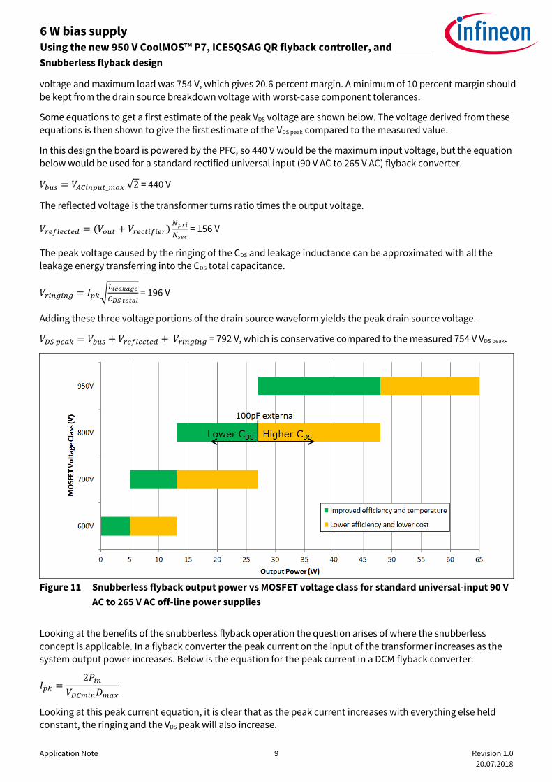
Figure 11 Snubberless flyback output power vs MOSFET voltage class for standard universal-input 90 V
AC to 265 V AC off-line power supplies
Looking at the benefits of the snubberless flyback operation the question arises of where the snubberless
concept is applicable. In a flyback converter the peak current on the input of the transformer increases as the system output power increases. Below is the equation for the peak current in a DCM flyback converter:
𝐼𝑝𝑘 =2𝑃𝑖𝑛
𝑉𝐷𝐶𝑚𝑖𝑛𝐷𝑚𝑎𝑥
Looking at this peak current equation, it is clear that as the peak current increases with everything else held constant, the ringing and the VDS peak will also increase.

Application Note 10 Revision 1.0
20.07.2018
6 W bias supply Using the new 950 V CoolMOS™ P7, ICE5QSAG QR flyback controller, and
snubberless flyback for improved auxiliary power supply efficiency and form-
factor Snubberless flyback design
𝑉𝑟𝑖𝑛𝑔𝑖𝑛𝑔 = 𝐼𝑝𝑘√𝐿𝑙𝑒𝑎𝑘𝑎𝑔𝑒
𝐶𝐷𝑆 𝑡𝑜𝑡𝑎𝑙
This leads to the chart shown above, which takes common charger adapter DCM flyback requirements and looks at the V(BR)DSS voltage required for different output powers. This shows that as the output power of the system increases a larger MOSFET breakdown voltage is required. This becomes a limiting factor in terms of where a
snubberless design can be used. Figure 11 does not match with this bias supply because the bias converter
needs to run off 440 V DC maximum rather than the standard 375 V DC that would be common in a universal-input AC-DC supply.
The other aspect shown in this chart is that a snubberless flyback converter can be designed with a larger and larger CDS to absorb the transformer leakage energy. There is a point where the required additional CDS
capacitance losses will match the RCD snubber losses, then the only benefit to the snubberless operation is
reduced PCB area and system cost. This boundary is shown above by the transition from green to yellow.
From the graph in Figure 11, it can be seen that for an efficiency benefit in snubberless operation devices with a
600 V breakdown should be used below 5 W, the 700 V devices should be used to 13 W, 800 V devices can be used to 27 W, and 950 V devices can be used to 48 W. Going beyond these boundaries would lower the system
efficiency. The above graph makes several assumptions about the system design operating point, so these should be taken as guidelines rather than hard boundaries.

Application Note 11 Revision 1.0
20.07.2018
6 W bias supply Using the new 950 V CoolMOS™ P7, ICE5QSAG QR flyback controller, and
snubberless flyback for improved auxiliary power supply efficiency and form-
factor Possible design changes
4 Possible design changes
4.1 Lowering the cost
The major element in terms of cost comes from the tantalum capacitors that were used to shrink the form factor. If cost is a priority, these capacitors can be replaced with 220 µF 16 V electrolytic capacitors to reduce
the overall system cost at the expense of space.

Application Note 12 Revision 1.0
20.07.2018
6 W bias supply Using the new 950 V CoolMOS™ P7, ICE5QSAG QR flyback controller, and
snubberless flyback for improved auxiliary power supply efficiency and form-
factor Demo board overview
5 Demo board overview
5.1 Demo board pictures
Figure 12 Top and bottom side of the 6 W bias board
5.2 Demo board specifications
Table 1
Section Parameter Specification
Input ratings Input voltage 120 V DC to 440 V DC
Efficiency @400 V DC, 6 W 85 percent
Output ratings Nominal output voltage 12.0 V DC
Output current 0.5 A
Switching frequency 25 kHz to 60 kHz
Mechanical Dimensions Length: 31.2 mm
Width: 35.1 mm
Height: 14.7 mm
Volume: 16.08 cm3
Environmental Ambient operating temperature -25°C to 50°C

Application Note 13 Revision 1.0
20.07.2018
6 W bias supply Using the new 950 V CoolMOS™ P7, ICE5QSAG QR flyback controller, and
snubberless flyback for improved auxiliary power supply efficiency and form-
factor Demo board overview
5.3 Schematic
Figure 13 6 W bias schematic

Application Note 14 Revision 1.0
20.07.2018
6 W bias supply Using the new 950 V CoolMOS™ P7, ICE5QSAG QR flyback controller, and
snubberless flyback for improved auxiliary power supply efficiency and form-
factor Demo board overview
5.4 PCB layout
The PCB was designed using Altium Designer 16. Schematic and board files are available on request.
Figure 14 Board layout – top and bottom
5.5 Transformer construction
The transformer was built by I.C.E. Transformers: http://www.icetransformers.com/
Table 2 Transformer specification
Manufacturer I.C.E. Transformers
Core size EFD20
Core material 3C95 or approved equivalent
Bobbin Pin shine EFD20 SMT S-2005
Primary inductance 5000 µH measured from pin 1 to pin 2 at 10 kHz
Leakage inductance Less than 50 µH measured from pin 1 to pin 2 at 10 kHz
Pins 5, 6, 7, 8 shorted
Note: 100 percent of components are Hi-Pot tested to 4.2 kV primary to secondary for 1 minute.
Pin-out viewed from the top of the bobbin:
Figure 15 Transformer windings stack-up and pin-out

Application Note 15 Revision 1.0
20.07.2018
6 W bias supply Using the new 950 V CoolMOS™ P7, ICE5QSAG QR flyback controller, and
snubberless flyback for improved auxiliary power supply efficiency and form-
factor Demo board overview
1. Place 3 mm of margin tape on the secondary side of the transformer (pins 7 to 12).
2. Place two turns of tape over the body of the entire assembly.
3. Place two turns of tape over the bottom of the transformer core or an insulator to provide creepage
isolation between pins and transformer core.
4. Clip pin 3.
Table 3
Name Start Stop Turns Wire gauge Layer Winding
P1 2 3 65 1 × ɸ 0.15 mm magnet wire Primary Evenly spaced
T1 2 Tape to fill window width
S1 7 8 10 1 × ɸ 0.5 mm triple insulated 12V_2 Evenly spaced
P3 6 5 10 1 × ɸ 0.5 mm triple insulated 12V_1 Evenly spaced
T2 2 Tape to fill window width
P2 3 1 65 1 × ɸ 0.15 mm magnet wire Primary Evenly spaced
T3 2 Tape to fill window width
5.6 Bill of Materials (BOM)
Table 1
Designator Qty Description Manufacturer Part number
C1 1 Ceramic capacitor, 10 pF, 1 kV, NP0, CAP1206 Kemet 1702125
C5 1 Ceramic capacitor, 22 nF, 1 kV, CAP1210 Murata 2456116
C6, C9 2 Ceramic capacitor, 1 µF, 25 V, X7R, CAP1206
C7 1 Electrolytic capacitor, 220 µF, 16 V Kemet 1793863
C8 1 Electrolytic capacitor, 220 µF, 16 V Kemet 1793863
C11 1 Ceramic capacitor, 22 µF, 25 V, X7R, CAP1210
C12 1 Ceramic capacitor, 0.1 µF, 25 V, X7R, CAP0805
C13 1 Ceramic capacitor, 1 nF, 25 V, NP0, CAP0805
C14 1 Ceramic capacitor, 220 pF, 25 V, NP0, CAP0805
C15 1 Ceramic capacitor, 1.5 nF, 25 V, X7R, CAP0805
D1 1 Schottky diode, BZX384-B2V4, SOD323 Nexperia 1727-3647-1-ND
D2 1 Schottky diode, BZX384-B15, SOD323 Nexperia 2319164
D9, D11 2 Standard diode, MBRS1100T3, SMB/DO-214AA 2317670
D12, D14 2 Medium-power AF Schottky diode, BAT165,
S0D250X125X110-2N
Infineon 1056502
D16 1 Schottky diode, BZX384-B11, SOD323 Nexperia 2319164
IC2 1 QR flyback controller, ICE5QSAG, SOIC8 Infineon ICE5QSAG
LED1 1 LED, 2.9 V, LED-0603R Rohm 2762564
Q2 1 n-MOSFET, BSS138N, SOT23R Infineon 2432717
R1 1 Resistor, 2 k, RES0805W Vishay 1469884
R2 1 Resistor, 33 R, RES0805R Vishay 1738939
R18 1 Resistor, 47 k, RES0805W Vishay 1469929

Application Note 16 Revision 1.0
20.07.2018
6 W bias supply Using the new 950 V CoolMOS™ P7, ICE5QSAG QR flyback controller, and
snubberless flyback for improved auxiliary power supply efficiency and form-
factor Demo board overview
Designator Qty Description Manufacturer Part number
R19, R22, R24 3 Resistor, 3.3 M, RES0805W
R20, R23, R25 3 Resistor, 10 M, RES0805W
R26 1 Resistor, 22 R, RES0805W
R27 1 Resistor, 3R3, RES0805W Vishay 2413965
R29 1 Resistor, 150 k, RES0805W
R30 1 Resistor, 47 R, RES0805W
R31 1 Resistor, 1 k, RES0805W
R32 1 Resistor, 10 k, RES0805W
T2 1 MOSFET, 950 V CoolMOS™ P7 Infineon IPU95R3K7P7
TF2 1 Flyback EFD20 12 V 6 W 8066.0103.030
X3 1 Pin header 5-pin Samtec 2041577
X4 1 Pin header 3-pin Samtec 2041576

Application Note 17 Revision 1.0
20.07.2018
6 W bias supply Using the new 950 V CoolMOS™ P7, ICE5QSAG QR flyback controller, and
snubberless flyback for improved auxiliary power supply efficiency and form-
factor Conclusion
6 Conclusion
This new bias board was designed to be a replacement for an existing bias module while using the latest devices available from Infineon. By switching to the latest available devices and to a snubberless flyback configuration, the efficiency is improved from 9.6 percent (full load point) to even 27 percent in light load condition Figure 2.
The 950 V CoolMOS™ P7 device helps to increase the breakdown voltage margin of the MOSFET as well as improve the efficiency by reducing the amount of switching losses caused by the external CDS required to enable snubberless operation. The strategies used in this converter, the latest Infineon components, QR operation, removing the snubber network, and an interleaved transformer design can also apply to other low-power bias flyback designs for an overall improvement in performance.

Application Note 18 Revision 1.0
20.07.2018
6 W bias supply Using the new 950 V CoolMOS™ P7, ICE5QSAG QR flyback controller, and
snubberless flyback for improved auxiliary power supply efficiency and form-
factor References
7 References
[1] ICE5QSAG QR Flyback Controller Datasheet
[2] IPU90R3K7P7 950V P7 MOSFET Datasheet

Application Note 19 Revision 1.0
20.07.2018
6 W bias supply Using the new 950 V CoolMOS™ P7, ICE5QSAG QR flyback controller, and
snubberless flyback for improved auxiliary power supply efficiency and form-
factor Revision history
Revision history
Major changes since the last revision
Page or reference Description of change

Published by
Infineon Technologies AG
81726 München, Germany
© 2020 Infineon Technologies AG.
All Rights Reserved.
Do you have a question about this
document?
Email: [email protected]
Document reference
IMPORTANT NOTICE The information given in this document shall in no event be regarded as a guarantee of conditions or characteristics (“Beschaffenheitsgarantie”) . With respect to any examples, hints or any typical values stated herein and/or any information regarding the application of the product, Infineon Technologies hereby disclaims any and all warranties and liabilities of any kind, including without limitation warranties of non-infringement of intellectual property rights of any third party. In addition, any information given in this document is subject to customer’s compliance with its obligations stated in this document and any applicable legal requirements, norms and standards concerning customer’s products and any use of the product of Infineon Technologies in customer’s applications. The data contained in this document is exclusively intended for technically trained staff. It is the responsibility of customer’s technical departments to evaluate the suitability of the product for the intended application and the completeness of the product information given in this document with respect to such application.
For further information on the product, technology, delivery terms and conditions and prices please contact your nearest Infineon Technologies office (www.infineon.com).
WARNINGS Due to technical requirements products may contain dangerous substances. For information on the types in question please contact your nearest Infineon Technologies office. Except as otherwise explicitly approved by Infineon Technologies in a written document signed by authorized representatives of Infineon Technologies, Infineon Technologies’ products may not be used in any applications where a failure of the product or any consequences of the use thereof can reasonably be expected to result in personal injury.
Edition 20.07.2018
AN_1801_PL52_1803_160336
Other Trademarks All referenced product or service names and trademarks are the property of their respective owners. AN_1801_PL52_1803_160336owners.