6 GHz Ultrahigh Dynamic Range Differential … GHz Ultrahigh Dynamic Range Differential Amplifier...
26
6 GHz Ultrahigh Dynamic Range Differential Amplifier Data Sheet ADL5565 Rev. F Document Feedback Information furnished by Analog Devices is believed to be accurate and reliable. However, no responsibility is assumed by Analog Devices for its use, nor for any infringements of patents or other rights of third parties that may result from its use. Specifications subject to change without notice. No license is granted by implication or otherwise under any patent or patent rights of Analog Devices. Trademarks and registered trademarks are the property of their respective owners. One Technology Way, P.O. Box 9106, Norwood, MA 02062-9106, U.S.A. Tel: 781.329.4700 ©2011–2017 Analog Devices, Inc. All rights reserved. Technical Support www.analog.com FEATURES 3 dB bandwidth of 6 GHz (AV = 6 dB) Pin strappable gain adjust: 6 dB, 12 dB, and 15.5 dB Gain range from 0 dB to 15.5 dB using two external resistors Differential or single-ended input to differential output Low noise input stage: NF = 8.7 dB at 15.5 dB gain Low broadband distortion (AV = 6 dB) 10 MHz: −107 dBc (HD2), −110 dBc (HD3) 100 MHz: −108 dBc (HD2), −103 dBc (HD3) 200 MHz: −82 dBc (HD2), −87 dBc (HD3) 500 MHz: −68 dBc (HD2), −63 dBc (HD3) IMD3 of −112 dBc at 100 MHz center Slew rate: 11 V/ns Fast settling and overdrive recovery of 2 ns Single-supply operation: 2.8 V to 5.2 V Power down Fabricated using the high speed XFCB3 SiGe process APPLICATIONS Differential ADC drivers Single-ended-to-differential conversion RF/IF gain blocks SAW filter interfacing FUNCTIONAL BLOCK DIAGRAM VIP2 ENBL R F R F VCOM VOP VIP1 VIN1 VIN2 ADL5565 GND VCC VON R G2 R G1 R G1 R G2 09959-001 Figure 1. GENERAL DESCRIPTION The ADL5565 is a high performance differential amplifier optimized for RF and IF applications. The amplifier offers low noise of 1.5 nV/√Hz and excellent distortion performance over a wide frequency range making it an ideal driver for high speed 8-bit to 16-bit analog-to-digital converters (ADCs). The ADL5565 provides three gain levels of 6 dB, 12 dB, and 15.5 dB through a pin strappable configuration. For the single- ended input configuration, the gains are reduced to 5.3 dB, 10.3 dB, and 13 dB. Using two external series resistors expands the gain flexibility of the amplifier and allows for any gain selection from 0 dB to 15.5 dB for a differential input and 0 dB to 13 dB for a single-ended input. The quiescent current of the ADL5565 is typically 70 mA, and when disabled, consumes less than 5 mA with −25 dB of input- to-output isolation at 100 MHz. The device is optimized for wideband, low distortion, and noise performance, giving it unprecedented performance for overall spurious-free dynamic range. These attributes, together with its adjustable gain capability, make this device the amplifier of choice for driving a wide variety of ADCs, mixers, pin diode attenuators, SAW filters, and multielement discrete devices. Fabricated on an Analog Devices, Inc., high speed SiGe process, the ADL5565 is supplied in a compact 3 mm × 3 mm, 16-lead LFCSP package and operates over the −40°C to +85°C temperature range.
Transcript of 6 GHz Ultrahigh Dynamic Range Differential … GHz Ultrahigh Dynamic Range Differential Amplifier...

6 GHz Ultrahigh Dynamic Range Differential Amplifier
Data Sheet ADL5565
Rev. F Document Feedback Information furnished by Analog Devices is believed to be accurate and reliable. However, no responsibility is assumed by Analog Devices for its use, nor for any infringements of patents or other rights of third parties that may result from its use. Specifications subject to change without notice. No license is granted by implication or otherwise under any patent or patent rights of Analog Devices. Trademarks and registered trademarks are the property of their respective owners.
One Technology Way, P.O. Box 9106, Norwood, MA 02062-9106, U.S.A. Tel: 781.329.4700 ©2011–2017 Analog Devices, Inc. All rights reserved. Technical Support www.analog.com
FEATURES 3 dB bandwidth of 6 GHz (AV = 6 dB) Pin strappable gain adjust: 6 dB, 12 dB, and 15.5 dB Gain range from 0 dB to 15.5 dB using two external resistors Differential or single-ended input to differential output Low noise input stage: NF = 8.7 dB at 15.5 dB gain Low broadband distortion (AV = 6 dB)
10 MHz: −107 dBc (HD2), −110 dBc (HD3) 100 MHz: −108 dBc (HD2), −103 dBc (HD3) 200 MHz: −82 dBc (HD2), −87 dBc (HD3) 500 MHz: −68 dBc (HD2), −63 dBc (HD3)
IMD3 of −112 dBc at 100 MHz center Slew rate: 11 V/ns Fast settling and overdrive recovery of 2 ns Single-supply operation: 2.8 V to 5.2 V Power down Fabricated using the high speed XFCB3 SiGe process
APPLICATIONS Differential ADC drivers Single-ended-to-differential conversion RF/IF gain blocks SAW filter interfacing
FUNCTIONAL BLOCK DIAGRAM
VIP2
ENBL
RF
RF
VCOM
VOP
VIP1
VIN1
VIN2
ADL5565GND
VCC
VONRG2
RG1
RG1
RG2
0995
9-00
1
Figure 1.
GENERAL DESCRIPTION The ADL5565 is a high performance differential amplifier optimized for RF and IF applications. The amplifier offers low noise of 1.5 nV/√Hz and excellent distortion performance over a wide frequency range making it an ideal driver for high speed 8-bit to 16-bit analog-to-digital converters (ADCs).
The ADL5565 provides three gain levels of 6 dB, 12 dB, and 15.5 dB through a pin strappable configuration. For the single-ended input configuration, the gains are reduced to 5.3 dB, 10.3 dB, and 13 dB. Using two external series resistors expands the gain flexibility of the amplifier and allows for any gain selection from 0 dB to 15.5 dB for a differential input and 0 dB to 13 dB for a single-ended input.
The quiescent current of the ADL5565 is typically 70 mA, and when disabled, consumes less than 5 mA with −25 dB of input-to-output isolation at 100 MHz.
The device is optimized for wideband, low distortion, and noise performance, giving it unprecedented performance for overall spurious-free dynamic range. These attributes, together with its adjustable gain capability, make this device the amplifier of choice for driving a wide variety of ADCs, mixers, pin diode attenuators, SAW filters, and multielement discrete devices.
Fabricated on an Analog Devices, Inc., high speed SiGe process, the ADL5565 is supplied in a compact 3 mm × 3 mm, 16-lead LFCSP package and operates over the −40°C to +85°C temperature range.

ADL5565 Data Sheet
Rev. F | Page 2 of 26
TABLE OF CONTENTS Features .............................................................................................. 1 Applications ....................................................................................... 1 Functional Block Diagram .............................................................. 1 General Description ......................................................................... 1 Revision History ............................................................................... 2 Specifications ..................................................................................... 3
3.3 V Specifications ...................................................................... 3 5 V Specifications ......................................................................... 6
Absolute Maximum Ratings ............................................................ 9 Thermal Resistance ...................................................................... 9 ESD Caution .................................................................................. 9
Pin Configuration and Function Descriptions ........................... 10 Typical Performance Characteristics ........................................... 11
Circuit Description......................................................................... 16 Basic Structure ............................................................................ 16
Applications Information .............................................................. 17 Basic Connections ...................................................................... 17 Input and Output Interfacing ................................................... 18 Gain Adjustment and Interfacing ............................................ 19 ADC Interfacing ......................................................................... 20 Layout Considerations ............................................................... 22 Soldering Information and Recommended PCB Land Pattern .......................................................................................... 23 Evaluation Board ........................................................................ 23
Outline Dimensions ....................................................................... 26 Ordering Guide .......................................................................... 26
REVISION HISTORY 11/2017—Rev. E to Rev. F CP-16-27 changed to CP-16-22 ................................... Throughout Updated Outline Dimensions ....................................................... 26 Changes to Ordering Guide .......................................................... 26 12/2013—Rev. D to Rev. E Updated Format .................................................................. Universal Changes to ENBL Threshold Parameter, Table 1 ......................... 3 Changes to ENBL Threshold Parameter, Table 2 ......................... 6 Changes to ENBL Pin Description, Table 5 ................................ 10 8/2013—Rev. C to Rev. D Changes to Features Section............................................................ 1 Changes to IMD3 Values in Table 1 ............................................... 4 Changes to IMD3 Values in Table 2 ............................................... 7 Changes to Figure14 ....................................................................... 12 Changes to Figure 15 ...................................................................... 13 12/2012—Rev. B to Rev. C Changes to Figure 25 ...................................................................... 14 Changes to Figure 27 and Figure 28 ............................................. 15 Changes to ADC Interfacing Section, Figure 37, and Figure 38 ... 20
6/2012—Rev. A to Rev. B Changes to Ordering Guide .......................................................... 26 4/2012—Rev. 0 to Rev. A Changes to Table 3; Added Thermal Resistance Section and Table 4, Renumbered Sequentially .................................................. 9 Deleted Soldering Information Section ....................................... 23 Added Soldering Information and Recommended PCB Land Pattern Section and Figure 44, Renumbered Sequentially ..................................................................................... 23 Updated Outline Dimensions ....................................................... 26 10/2011—Revision 0: Initial Version

Data Sheet ADL5565
Rev. F | Page 3 of 26
SPECIFICATIONS 3.3 V SPECIFICATIONS VS = 3.3 V, VCM = 1.65 V, RL = 200 Ω differential, AV = 6 dB, CL = 1 pF differential, f = 100 MHz, TA = 25°C; parameters specified ac-coupled differential input and differential output, unless otherwise noted.
Table 1. Parameter Test Conditions/Comments Min Typ Max Unit DYNAMIC PERFORMANCE
−3 dB Bandwidth AV = 6 dB, VOUT ≤ 1.0 V p-p 6750 MHz AV = 12 dB, VOUT ≤ 1.0 V p-p 6500 MHz
AV = 15.5 dB, VOUT ≤ 1.0 V p-p 6250 MHz Bandwidth for 0.1 dB Flatness VOUT ≤ 1.0 V p-p 1000 MHz Gain Accuracy ±1 dB Gain Supply Sensitivity VS ± 5% 1.9 mdB/V Gain Temperature Sensitivity −40°C to +85°C 0.35 mdB/°C Slew Rate Rise, AV = 15.5 dB, RL = 200 Ω,
VOUT = 2 V step 11 V/ns
Fall, AV = 15.5 dB, RL = 200 Ω, VOUT = 2 V step
11 V/ns
Settling Time 2 V step to 1% 2 ns Overdrive Recovery Time VIN = 4 V to 0 V step, VOUT ≤ ±10 mV <3 ns Reverse Isolation (S12) 70 dB
INPUT/OUTPUT CHARACTERISTICS Input Common-Mode Range AV = 6 dB, 12 dB, and 15.5 dB 1.2 to 2 V Output Common-Mode Range 1.4 to 1.8 V Maximum Output Voltage Swing 1 dB compressed 4 V p-p Output Common-Mode Offset Referenced to VCC/2 −100 +20 mV Output Common-Mode Drift −40°C to +85°C 0.34 mV/°C Output Differential Offset Voltage −20 +20 mV CMRR 60 dB Output Differential Offset Drift −40°C to +85°C 1.5 mV/°C Input Bias Current ±5 µA Input Resistance (Differential) AV = 6 dB 200 Ω AV = 12 dB 100 Ω AV = 15.5 dB 67 Ω Input Resistance (Single-Ended) AV = 5.6 dB 158 Ω AV = 11.1 dB 96 Ω AV = 14.1 dB 74 Ω Input Capacitance (Single-Ended) 0.3 pF Output Resistance (Differential) 10 Ω
POWER INTERFACE Supply Voltage 2.8 3.3 5.2 V ENBL Threshold Device disabled, ENBL low 0.5 V Device enabled, ENBL high 1.5 V ENBL Input Bias Current ENBL high 500 nA ENBL low −165 µA Quiescent Current ENBL high 70 mA ENBL low 5 mA
ADL5565 Data Sheet
Rev. F | Page 4 of 26
Parameter Test Conditions/Comments Min Typ Max Unit NOISE/HARMONIC PERFORMANCE
10 MHz Second/Third Harmonic Distortion (HD2/HD3) AV = 6 dB, RL = 200 Ω, VOUT = 2 V p-p −107/−110 dBc AV = 12 dB, RL = 200 Ω, VOUT = 2 V p-p −101/−107 dBc AV = 15.5 dB, RL = 200 Ω, VOUT = 2 V p-p −106/−112 dBc Output IP3/Third-Order Intermodulation
Distortion (OIP3/IMD3) AV = 6 dB, RL = 200 Ω, VOUT = 2 V p-p composite (2 MHz spacing)
+48/−100 dBm/dBc
AV = 12 dB, RL = 200 Ω, VOUT = 2 V p-p composite (2 MHz spacing)
+52/−108 dBm/dBc
AV = 15.5 dB, RL = 200 Ω, VOUT = 2 V p-p composite (2 MHz spacing)
+50/−104 dBm/dBc
Second-Order Intermodulation Distortion (IMD2) AV = 6 dB, RL = 200 Ω, VOUT = 2 V p-p composite (2 MHz spacing)
−86 dBc
AV = 12 dB, RL = 200 Ω, VOUT = 2 V p-p composite (2 MHz spacing)
−86 dBc
AV = 15.5 dB, RL = 200 Ω, VOUT = 2 V p-p composite (2 MHz spacing)
−86 dBc
Noise Spectral Density, RTI (NSD) AV = 6 dB 2.24 nV/√Hz AV = 12 dB 1.52 nV/√Hz AV = 15.5 dB 1.53 nV/√Hz Noise Figure (NF) AV = 6 dB 10.24 dB AV = 12 dB 8.66 dB AV = 15.5 dB 8.78 dB 1 dB Compression Point, RTO (OP1dB) AV = 6 dB 13.1 dBm
AV = 12 dB 12.8 dBm AV = 15.5 dB 13.1 dBm 100 MHz
Second/Third Harmonic Distortion (HD2/HD3) AV = 6 dB, RL = 200 Ω, VOUT = 2 V p-p −108/−103 dBc AV = 12 dB, RL = 200 Ω, VOUT = 2 V p-p −91/−99 dBc AV = 15.5 dB, RL = 200 Ω, VOUT = 2 V p-p −89/−100 dBc Output IP3/Third-Order Intermodulation
Distortion (OIP3/IMD3) AV = 6 dB, RL = 200 Ω, VOUT = 2 V p-p composite (2 MHz spacing)
+54/−112 dBm/dBc
AV = 12 dB, RL = 200 Ω, VOUT = 2 V p-p composite (2 MHz spacing)
+53/−110 dBm/dBc
AV = 15.5 dB, RL = 200 Ω, VOUT = 2 V p-p composite (2 MHz spacing)
+52/−108 dBm/dBc
Second-Order Intermodulation Distortion (IMD2) AV = 6 dB, RL = 200 Ω, VOUT = 2 V p-p composite (2 MHz spacing)
−85 dBc
AV = 12 dB, RL = 200 Ω, VOUT = 2 V p-p composite (2 MHz spacing)
−85 dBc
AV = 15.5 dB, RL = 200 Ω, VOUT = 2 V p-p composite (2 MHz spacing)
−86 dBc
Noise Spectral Density, RTI (NSD) AV = 6 dB 2.25 nV/√Hz AV = 12 dB 1.53 nV/√Hz AV = 15.5 dB 1.52 nV/√Hz Noise Figure (NF) AV = 6 dB 10.27 dB AV = 12 dB 8.69 dB AV = 15.5 dB 8.7 dB 1 dB Compression Point, RTO (OP1dB) AV = 6 dB 13 dBm
AV = 12 dB 12.8 dBm AV = 15.5 dB 12.8 dBm
Data Sheet ADL5565
Rev. F | Page 5 of 26
Parameter Test Conditions/Comments Min Typ Max Unit 200 MHz
Second/Third Harmonic Distortion (HD2/HD3) AV = 6 dB, RL = 200 Ω, VOUT = 2 V p-p −82/−87 dBc AV = 12 dB, RL = 200 Ω, VOUT = 2 V p-p −72/−86 dBc AV = 15.5 dB, RL = 200 Ω, VOUT = 2 V p-p −71/−86 dBc Output IP3/Third-Order Intermodulation
Distortion (OIP3/IMD3) AV = 6 dB, RL = 200 Ω, VOUT = 2 V p-p composite
+46/−96 dBm/dBc
AV = 12 dB, RL = 200 Ω, VOUT = 2 V p-p composite
+46/−96 dBm/dBc
AV = 15.5 dB, RL = 200 Ω, VOUT = 2 V p-p composite
+46/−96 dBm/dBc
Second-Order Intermodulation Distortion (IMD2) AV = 6 dB, RL = 200 Ω, VOUT = 2 V p-p composite (2 MHz spacing)
−85 dBc
AV = 12 dB, RL = 200 Ω, VOUT = 2 V p-p composite (2 MHz spacing)
−73 dBc
AV = 15.5 dB, RL = 200 Ω, VOUT = 2 V p-p composite (2 MHz spacing)
−70 dBc
Noise Spectral Density, RTI (NSD) AV = 6 dB 2.36 nV/√Hz AV = 12 dB 1.64 nV/√Hz AV = 15.5 dB 1.51 nV/√Hz Noise Figure (NF) AV = 6 dB 10.65 dB
AV = 12 dB 9.25 dB AV = 15.5 dB 8.49 dB 500 MHz
Second/Third Harmonic Distortion (HD2/HD3) AV = 6 dB, RL = 200 Ω, VOUT = 2 V p-p −68/−63 dBc AV = 12 dB, RL = 200 Ω, VOUT = 2 V p-p −56/−62 dBc AV = 15.5 dB, RL = 200 Ω, VOUT = 2 V p-p −57/−63 dBc Output IP3/Third-Order Intermodulation
Distortion (OIP3/IMD3) AV = 6 dB, RL = 200 Ω, VOUT = 2 V p-p composite
+34/−72 dBm/dBc
AV = 12 dB, RL = 200 Ω, VOUT = 2 V p-p composite
+36/−76 dBm/dBc
AV = 15.5 dB, RL = 200 Ω, VOUT = 2 V p-p composite
+39/−82 dBm/dBc
Second-Order Intermodulation Distortion (IMD2) AV = 6 dB, RL = 200 Ω, VOUT = 2 V p-p composite (2 MHz spacing)
−75 dBc
AV = 12 dB, RL = 200 Ω, VOUT = 2 V p-p composite (2 MHz spacing)
−70 dBc
AV = 15.5 dB, RL = 200 Ω, VOUT = 2 V p-p composite (2 MHz spacing)
−70 dBc
Noise Spectral Density, RTI (NSD) AV = 6 dB 2.62 nV/√Hz AV = 12 dB 1.57 nV/√Hz AV = 15.5 dB 1.47 nV/√Hz Noise Figure (NF) AV = 6 dB 11.47 dB
AV = 12 dB 8.93 dB AV = 15.5 dB 8.07 dB

ADL5565 Data Sheet
Rev. F | Page 6 of 26
5 V SPECIFICATIONS VS = 5.0 V, VCM = 2.5 V, RL = 200 Ω differential, AV = 6 dB, CL = 1 pF differential, f = 100 MHz, TA = 25°C; parameters specified ac-coupled differential input and differential output, unless otherwise noted.
Table 2. Parameter Test Conditions/Comments Min Typ Max Unit DYNAMIC PERFORMANCE
−3 dB Bandwidth AV = 6 dB, VOUT ≤ 1.0 V p-p 7000 MHz AV = 12 dB, VOUT ≤ 1.0 V p-p 6750 MHz
AV = 15.5 dB, VOUT ≤ 1.0 V p-p 6500 MHz Bandwidth for 0.1 dB Flatness VOUT ≤ 1.0 V p-p 1000 MHz Gain Accuracy ±1 dB Gain Supply Sensitivity VS ± 5% 1.6 mdB/V Gain Temperature Sensitivity −40°C to +85°C 0.37 mdB/°C Slew Rate Rise, AV = 15.5 dB, RL = 200 Ω,
VOUT = 2 V step 11 V/ns
Fall, AV = 15.5 dB, RL = 200 Ω, VOUT = 2 V step
11 V/ns
Settling Time 2 V step to 1% 2 ns Overdrive Recovery Time VIN = 4 V to 0 V step, VOUT ≤ ±10 mV <3 ns Reverse Isolation (S12) 70 dB
INPUT/OUTPUT CHARACTERISTICS Input Common-Mode Range AV = 6 dB, 12 dB, and 15.5 dB 1.2 to 3.8 V Output Common-Mode Range 1.4 to 3 V Maximum Output Voltage Swing 1 dB compressed 8 V p-p Output Common-Mode Offset Referenced to VCC/2 −100 +20 mV Output Common-Mode Drift −40°C to +85°C 0.4 mV/°C Output Differential Offset Voltage −20 +20 mV CMRR 60 dB Output Differential Offset Drift −40°C to +85°C 1.5 mV/°C Input Bias Current ±5 µA Input Resistance (Differential) AV = 6 dB 200 Ω AV = 12 dB 100 Ω AV = 15.5 dB 67 Ω Input Resistance (Single-Ended) AV = 5.6 dB 158 Ω AV = 11.1 dB 96 Ω AV = 14.1 dB 74 Ω Input Capacitance (Single-Ended) 0.3 pF Output Resistance (Differential) 10 Ω
POWER INTERFACE Supply Voltage 2.8 5 5.2 V ENBL Threshold Device disabled, ENBL low 0.6 V Device enabled, ENBL high 1.5 V ENBL Input Bias Current ENBL high 1 µA ENBL low −250 µA Quiescent Current ENBL high 80 mA ENBL low 6 mA
Data Sheet ADL5565
Rev. F | Page 7 of 26
Parameter Test Conditions/Comments Min Typ Max Unit NOISE/HARMONIC PERFORMANCE
10 MHz Second/Third Harmonic Distortion (HD2/HD3) AV = 6 dB, RL = 200 Ω, VOUT = 2 V p-p −111/−116 dBc AV = 12 dB, RL = 200 Ω, VOUT = 2 V p-p −100/−104 dBc AV = 15.5 dB, RL = 200 Ω, VOUT = 2 V p-p −105/−106 dBc Output IP3/Third-Order Intermodulation
Distortion (OIP3/IMD3) AV = 6 dB, RL = 200 Ω, VOUT = 2 V p-p composite (2 MHz spacing)
+47/−98 dBm/dBc
AV = 12 dB, RL = 200 Ω, VOUT = 2 V p-p composite (2 MHz spacing)
+50/−104 dBm/dBc
AV = 15.5 dB, RL = 200 Ω, VOUT = 2 V p-p composite (2 MHz spacing)
+50/−104 dBm/dBc
Second-Order Intermodulation Distortion (IMD2) AV = 6 dB, RL = 200 Ω, VOUT = 2 V p-p composite (2 MHz spacing)
−78 dBc
AV = 12 dB, RL = 200 Ω, VOUT = 2 V p-p composite (2 MHz spacing)
−86 dBc
AV = 15.5 dB, RL = 200 Ω, VOUT = 2 V p-p composite (2 MHz spacing)
−91 dBc
Noise Spectral Density, RTI (NSD) AV = 6 dB 2.25 nV/√Hz AV = 12 dB 1.54 nV/√Hz AV = 15.5 dB 1.55 nV/√Hz Noise Figure (NF) AV = 6 dB 10.29 dB AV = 12 dB 8.77 dB AV = 15.5 dB 9.04 dB 1 dB Compression Point, RTO (OP1dB) AV = 6 dB 16.8 dBm
AV = 12 dB 16.7 dBm AV = 15.5 dB 16.6 dBm
100 MHz Second/Third Harmonic Distortion (HD2/HD3) AV = 6 dB, RL = 200 Ω, VOUT = 2 V p-p −108/−109 dBc AV = 12 dB, RL = 200 Ω, VOUT = 2 V p-p −92/−103 dBc AV = 15.5 dB, RL = 200 Ω, VOUT = 2 V p-p −89.5/−105 dBc Output IP3/Third-Order Intermodulation
Distortion (OIP3/IMD3) AV = 6 dB, RL = 200 Ω, VOUT = 2 V p-p composite (2 MHz spacing)
+53/−110 dBm/dBc
AV = 12 dB, RL = 200 Ω, VOUT = 2 V p-p composite (2 MHz spacing)
+53/−110 dBm/dBc
AV = 15.5 dB, RL = 200 Ω, VOUT = 2 V p-p composite (2 MHz spacing)
+52/−108 dBm/dBc
Second-Order Intermodulation Distortion (IMD2) AV = 6 dB, RL = 200 Ω, VOUT = 2 V p-p composite (2 MHz spacing)
−87 dBc
AV = 12 dB, RL = 200 Ω, VOUT = 2 V p-p composite (2 MHz spacing)
−91 dBc
AV = 15.5 dB, RL = 200 Ω, VOUT = 2 V p-p composite (2 MHz spacing)
−87 dBc
Noise Spectral Density, RTI (NSD) AV = 6 dB 2.28 nV/√Hz AV = 12 dB 1.53 nV/√Hz AV = 15.5 dB 1.52 nV/√Hz Noise Figure (NF) AV = 6 dB 10.39 dB AV = 12 dB 8.73 dB AV = 15.5 dB 8.7 dB 1 dB Compression Point, RTO (OP1dB) AV = 6 dB 16.8 dBm AV = 12 dB 16.5 dBm
AV = 15.5 dB 16.4 dBm

ADL5565 Data Sheet
Rev. F | Page 8 of 26
Parameter Test Conditions/Comments Min Typ Max Unit 200 MHz
Second/Third Harmonic Distortion (HD2/HD3) AV = 6 dB, RL = 200 Ω, VOUT = 2 V p-p −82/−87 dBc AV = 12 dB, RL = 200 Ω, VOUT = 2 V p-p −72/−86 dBc AV = 15.5 dB, RL = 200 Ω, VOUT = 2 V p-p −71/−86 dBc Output IP3/Third-Order Intermodulation
Distortion (OIP3/IMD3) AV = 6 dB, RL = 200 Ω, VOUT = 2 V p-p composite
+46/−96 dBm/dBc
AV = 12 dB, RL = 200 Ω, VOUT = 2 V p-p composite
+46/−96 dBm/dBc
AV = 15.5 dB, RL = 200 Ω, VOUT = 2 V p-p composite
+46/−96 dBm/dBc
Second-Order Intermodulation Distortion (IMD2) AV = 6 dB, RL = 200 Ω, VOUT = 2 V p-p composite (2 MHz spacing)
−85 dBc
AV = 12 dB, RL = 200 Ω, VOUT = 2 V p-p composite (2 MHz spacing)
−74 dBc
AV = 15.5 dB, RL = 200 Ω, VOUT = 2 V p-p composite (2 MHz spacing)
−70 dBc
Noise Spectral Density, RTI (NSD) AV = 6 dB 2.43 nV/√Hz AV = 12 dB 1.63 nV/√Hz AV = 15.5 dB 1.51 nV/√Hz Noise Figure (NF) AV = 6 dB 10.88 dB
AV = 12 dB 9.2 dB AV = 15.5 dB 8.54 dB 500 MHz
Second/Third Harmonic Distortion (HD2/HD3) AV = 6 dB, RL = 200 Ω, VOUT = 2 V p-p −69/−66 dBc AV = 12 dB, RL = 200 Ω, VOUT = 2 V p-p −56/−65 dBc AV = 15.5 dB, RL = 200 Ω, VOUT = 2 V p-p −58/−66 dBc Output IP3/Third-Order Intermodulation
Distortion (OIP3/IMD3) AV = 6 dB, RL = 200 Ω, VOUT = 2 V p-p composite
+35/−74 dBm/dBc
AV = 12 dB, RL = 200 Ω, VOUT = 2 V p-p composite
+35/−74 dBm/dBc
AV = 15.5 dB, RL = 200 Ω, VOUT = 2 V p-p composite
+37/−78 dBm/dBc
Second-Order Intermodulation Distortion (IMD2) AV = 6 dB, RL = 200 Ω, VOUT = 2 V p-p composite (2 MHz spacing)
−73 dBc
AV = 12 dB, RL = 200 Ω, VOUT = 2 V p-p composite (2 MHz spacing)
−75 dBc
AV = 15.5 dB, RL = 200 Ω, VOUT = 2 V p-p composite (2 MHz spacing)
−72 dBc
Noise Spectral Density, RTI (NSD) AV = 6 dB 2.64 nV/√Hz AV = 12 dB 1.6 nV/√Hz AV = 15.5 dB 1.48 nV/√Hz Noise Figure (NF) AV = 6 dB 11.56 dB AV = 12 dB 9.06 dB
AV = 15.5 dB 8.17 dB

Data Sheet ADL5565
Rev. F | Page 9 of 26
ABSOLUTE MAXIMUM RATINGS Table 3. Parameter Rating Output Voltage Swing × Bandwidth Product 2000 V p-p MHz Supply Voltage, VCC 5.25 V VIPx, VINx VCC + 0.5 V ±IOUT Maximum 30 mA Internal Power Dissipation 525 mW Maximum Junction Temperature 125°C Operating Temperature Range −40°C to +100°C Storage Temperature Range −65°C to +150°C
Stresses at or above those listed under Absolute Maximum Ratings may cause permanent damage to the product. This is a stress rating only; functional operation of the product at these or any other conditions above those indicated in the operational section of this specification is not implied. Operation beyond the maximum operating conditions for extended periods may affect product reliability.
THERMAL RESISTANCE Table 4 lists the junction-to-air thermal resistance (θJA) and the junction-to-paddle thermal resistance (θJC) for the ADL5565.
Table 4. Thermal Resistance Package Type θJA
1 θJC2 Unit
16-Lead LFCSP 60 12 °C/W
1 Measured on Analog Devices evaluation board. For more information about board layout, see the Soldering Information and Recommended PCB Land Pattern section.
2 Based on simulation with JEDEC standard JESD51.
ESD CAUTION
ADL5565 Data Sheet
Rev. F | Page 10 of 26
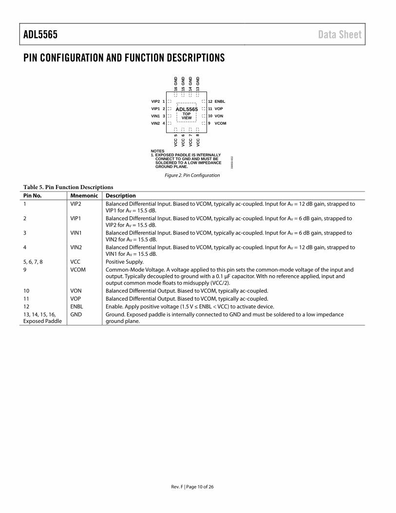
PIN CONFIGURATION AND FUNCTION DESCRIPTIONS
VIP2
VIP1
VIN1
VIN2
VOP
ENBL
VON
VCOM
VCC
VCC
VCC
VCC
GN
D
GN
D
GN
D
GN
D
NOTES1. EXPOSED PADDLE IS INTERNALLY CONNECT TO GND AND MUST BE SOLDERED TO A LOW IMPEDANCE GROUND PLANE.
12
11
10
1
3
4 9
2
65 7 8
16 15 14 13
TOPVIEW
ADL5565
0995
9-00
2
Figure 2. Pin Configuration
Table 5. Pin Function Descriptions Pin No. Mnemonic Description 1 VIP2 Balanced Differential Input. Biased to VCOM, typically ac-coupled. Input for AV = 12 dB gain, strapped to
VIP1 for AV = 15.5 dB. 2 VIP1 Balanced Differential Input. Biased to VCOM, typically ac-coupled. Input for AV = 6 dB gain, strapped to
VIP2 for AV = 15.5 dB. 3 VIN1 Balanced Differential Input. Biased to VCOM, typically ac-coupled. Input for AV = 6 dB gain, strapped to
VIN2 for AV = 15.5 dB. 4 VIN2 Balanced Differential Input. Biased to VCOM, typically ac-coupled. Input for AV = 12 dB gain, strapped to
VIN1 for AV = 15.5 dB. 5, 6, 7, 8 VCC Positive Supply. 9 VCOM Common-Mode Voltage. A voltage applied to this pin sets the common-mode voltage of the input and
output. Typically decoupled to ground with a 0.1 µF capacitor. With no reference applied, input and output common mode floats to midsupply (VCC/2).
10 VON Balanced Differential Output. Biased to VCOM, typically ac-coupled. 11 VOP Balanced Differential Output. Biased to VCOM, typically ac-coupled. 12 ENBL Enable. Apply positive voltage (1.5 V ≤ ENBL < VCC) to activate device. 13, 14, 15, 16, Exposed Paddle
GND Ground. Exposed paddle is internally connected to GND and must be soldered to a low impedance ground plane.
Data Sheet ADL5565
Rev. F | Page 11 of 26
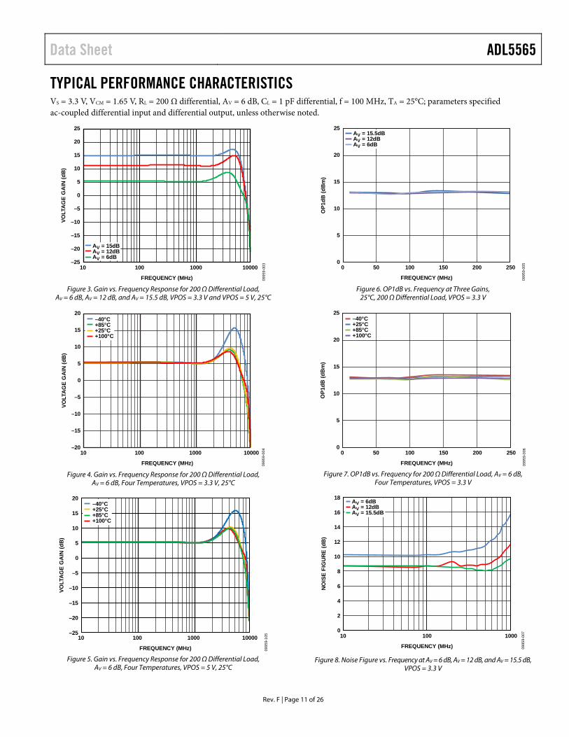
TYPICAL PERFORMANCE CHARACTERISTICS VS = 3.3 V, VCM = 1.65 V, RL = 200 Ω differential, AV = 6 dB, CL = 1 pF differential, f = 100 MHz, TA = 25°C; parameters specified ac-coupled differential input and differential output, unless otherwise noted.
–25
–20
–15
–10
–5
0
5
10
15
20
25
10 100 1000 10000
VOLT
AG
E G
AIN
(dB
)
FREQUENCY (MHz)
AV = 15dBAV = 12dBAV = 6dB
0995
9-00
3
Figure 3. Gain vs. Frequency Response for 200 Ω Differential Load, AV = 6 dB, AV = 12 dB, and AV = 15.5 dB, VPOS = 3.3 V and VPOS = 5 V, 25°C
–20
–15
–10
–5
0
5
10
15
20
10 100 100001000
VOLT
AG
E G
AIN
(dB
)
FREQUENCY (MHz)
–40°C+85°C+25°C+100°C
0995
9-00
4
Figure 4. Gain vs. Frequency Response for 200 Ω Differential Load, AV = 6 dB, Four Temperatures, VPOS = 3.3 V, 25°C
10 100 100001000
VOLT
AG
E G
AIN
(dB
)
FREQUENCY (MHz)
–25
–20
–15
–10
–5
0
5
10
15
20–40°C+25°C+85°C+100°C
0995
9-10
5
Figure 5. Gain vs. Frequency Response for 200 Ω Differential Load, AV = 6 dB, Four Temperatures, VPOS = 5 V, 25°C
0
5
10
15
20
25
0 50 100 150 200 250
OP1
dB (d
Bm
)
FREQUENCY (MHz) 0995
9-00
5
AV = 15.5dBAV = 12dBAV = 6dB
Figure 6. OP1dB vs. Frequency at Three Gains, 25°C, 200 Ω Differential Load, VPOS = 3.3 V
0
5
10
15
20
25
0 50 100 150 200 250
OP1
dB (d
Bm
)
FREQUENCY (MHz)
–40°C+25°C+85°C+100°C
0995
9-00
6
Figure 7. OP1dB vs. Frequency for 200 Ω Differential Load, AV = 6 dB, Four Temperatures, VPOS = 3.3 V
0
2
4
6
8
10
12
14
16
18
10 100 1000
NO
ISE
FIG
UR
E (d
B)
FREQUENCY (MHz) 0995
9-00
7
AV = 6dBAV = 12dBAV = 15.5dB
Figure 8. Noise Figure vs. Frequency at AV = 6 dB, AV = 12 dB, and AV = 15.5 dB, VPOS = 3.3 V
ADL5565 Data Sheet
Rev. F | Page 12 of 26
0
2
4
6
8
10
12
14
16
18
10M 100M 1G
NO
ISE
FIG
UR
E (d
B)
FREQUENCY (Hz)
AV = 6dBAV = 12dBAV = 15.5dB
0995
9-00
8
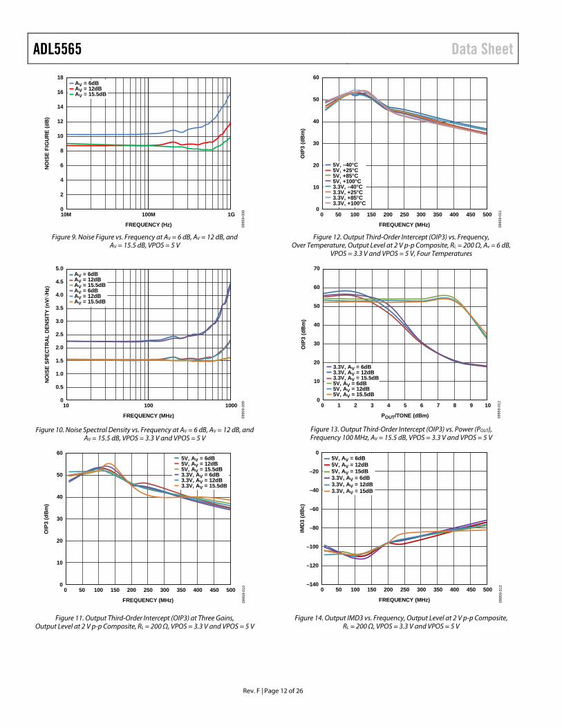
Figure 9. Noise Figure vs. Frequency at AV = 6 dB, AV = 12 dB, and
AV = 15.5 dB, VPOS = 5 V
10 100 1000
FREQUENCY (MHz)
0
0.5
1.0
1.5
2.0
2.5
3.0
3.5
4.0
4.5
5.0
NO
ISE
SPEC
TRA
L D
ENSI
TY (n
V/√H
z)
AV = 6dBAV = 12dBAV = 15.5dBAV = 6dBAV = 12dBAV = 15.5dB
0995
9-00
9
Figure 10. Noise Spectral Density vs. Frequency at AV = 6 dB, AV = 12 dB, and AV = 15.5 dB, VPOS = 3.3 V and VPOS = 5 V
0
10
20
30
40
50
60
0 50 100 150 200 250 300 350 400 450 500
OIP
3 (d
Bm
)
FREQUENCY (MHz)
5V, AV = 6dB5V, AV = 12dB5V, AV = 15.5dB3.3V, AV = 6dB3.3V, AV = 12dB3.3V, AV = 15.5dB
0995
9-01
0
Figure 11. Output Third-Order Intercept (OIP3) at Three Gains, Output Level at 2 V p-p Composite, RL = 200 Ω, VPOS = 3.3 V and VPOS = 5 V
0
10
20
30
40
50
60
0 50 100 150 200 250 300 350 400 450 500
OIP
3 (d
Bm
)
FREQUENCY (MHz)
5V, –40°C5V, +25°C5V, +85°C5V, +100°C3.3V, –40°C3.3V, +25°C3.3V, +85°C3.3V, +100°C
0995
9-01
1
Figure 12. Output Third-Order Intercept (OIP3) vs. Frequency,
Over Temperature, Output Level at 2 V p-p Composite, RL = 200 Ω, Av = 6 dB, VPOS = 3.3 V and VPOS = 5 V, Four Temperatures
0
10
20
30
40
50
60
70
0 1 2 3 4 5 6 7 8 9 10
OIP
3 (d
Bm
)
POUT/TONE (dBm)
3.3V, AV = 6dB3.3V, AV = 12dB3.3V, AV = 15.5dB5V, AV = 6dB5V, AV = 12dB5V, AV = 15.5dB
0995
9-01
2
Figure 13. Output Third-Order Intercept (OIP3) vs. Power (POUT), Frequency 100 MHz, AV = 15.5 dB, VPOS = 3.3 V and VPOS = 5 V
–140
–120
–100
–80
–60
–40
–20
0
0 50 100 150 200 250 300 350 400 450 500
IMD
3 (d
Bc)
FREQUENCY (MHz) 0995
9-01
3
5V, AV = 6dB5V, AV = 12dB5V, AV = 15dB3.3V, AV = 6dB3.3V, AV = 12dB3.3V, AV = 15dB
Figure 14. Output IMD3 vs. Frequency, Output Level at 2 V p-p Composite, RL = 200 Ω, VPOS = 3.3 V and VPOS = 5 V
Data Sheet ADL5565
Rev. F | Page 13 of 26
–140
–120
–100
–80
–60
–40
–20
0
0 50 100 150 200 250 300 350 400 450 500
IMD
3 (d
Bm
)
FREQUENCY (MHz) 0995
9-01
4
5V, –40°C5V, +25°C5V, +85°C5V, +100°C3.3V, –40°C3.3V, +25°C3.3V, +85°C3.3V, +100°C
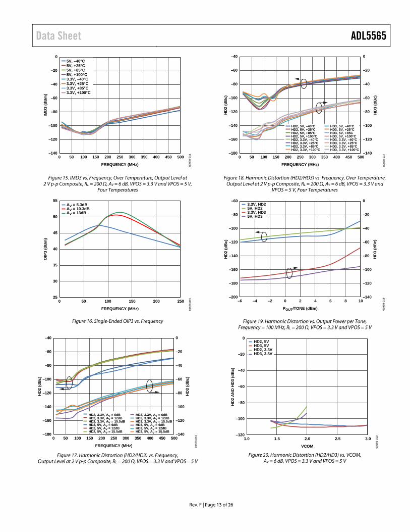
Figure 15. IMD3 vs. Frequency, Over Temperature, Output Level at 2 V p-p Composite, RL = 200 Ω, AV = 6 dB, VPOS = 3.3 V and VPOS = 5 V,
Four Temperatures
25
30
35
40
45
50
55
0 50 100 150 200 250
OIP
3 (d
Bm
)
FREQUENCY (MHz) 0995
9-01
5
AV = 5.3dBAV = 10.3dBAV = 13dB
Figure 16. Single-Ended OIP3 vs. Frequency
–140
–120
–100
–80
–60
–40
–20
0
–180
–160
–140
–120
–100
–80
–60
–40
0 50 100 150 200 250 300 350 400 450 500
HD
3 (d
Bc)
HD
2 (d
Bc)
FREQUENCY (MHz)
HD2, 3.3V, AV = 6dBHD2, 3.3V, AV = 12dBHD2, 3.3V, AV = 15.5dBHD2, 5V, AV = 6dBHD2, 5V, AV = 12dBHD2, 5V, AV = 15.5dB
HD3, 3.3V, AV = 6dBHD3, 3.3V, AV = 12dBHD3, 3.3V, AV = 15.5dBHD3, 5V, AV = 6dBHD3, 5V, AV = 12dBHD3, 5V, AV = 15.5dB
0995
9-01
6
Figure 17. Harmonic Distortion (HD2/HD3) vs. Frequency, Output Level at 2 V p-p Composite, RL = 200 Ω, VPOS = 3.3 V and VPOS = 5 V
–140
–120
–100
–80
–60
–40
–20
0
–180
–160
–140
–120
–100
–80
–60
–40
0 50 100 150 200 250 300 350 400 450 500
HD
3 (d
Bc)
HD
2 (d
Bc)
FREQUENCY (MHz)
HD2, 5V, –40°CHD2, 5V, +25°CHD2, 5V, +85°CHD2, 5V, +100°CHD2, 3.3V, –40°CHD2, 3.3V, +25°CHD2, 3.3V, +85°CHD2, 3.3V, +100°C
HD3, 5V, –40°CHD3, 5V, +25°CHD3, 5V, +85CHD3, 5V, +100°CHD3, 3.3V, –40°CHD3, 3.3V, +25°CHD3, 3.3V, +85°CHD3, 3.3V, +100°C
0995
9-01
7
Figure 18. Harmonic Distortion (HD2/HD3) vs. Frequency, Over Temperature, Output Level at 2 V p-p Composite, RL = 200 Ω, AV = 6 dB, VPOS = 3.3 V and
VPOS = 5 V, Four Temperatures
POUT/TONE (dBm)
–140
–120
–100
–80
–60
–40
–20
0
–200
–180
–160
–140
–120
–100
–80
–60
–6 –4 –2 0 2 4 6 8 10
HD
3 (d
Bc)
HD
2 (d
Bc)
3.3V, HD25V, HD23.3V, HD35V, HD3
0995
9-01
8
Figure 19. Harmonic Distortion vs. Output Power per Tone, Frequency = 100 MHz, RL = 200 Ω, VPOS = 3.3 V and VPOS = 5 V
–120
–100
–80
–60
–40
–20
0
1.0 1.5 2.0 2.5 3.0
HD
2A
ND
HD
3 (d
Bc)
VCOM
HD2, 5VHD3, 5VHD2, 3.3VHD3, 3.3V
0995
9-01
9
Figure 20. Harmonic Distortion (HD2/HD3) vs. VCOM,
AV = 6 dB, VPOS = 3.3 V and VPOS = 5 V
ADL5565 Data Sheet
Rev. F | Page 14 of 26
–105
–100
–95
–90
–85
–80
–75
–70
–65
–60
0 50 100 150 200 250 300
HA
RM
ON
IC D
IST
OR
TIO
N H
D2,
HD
3 (d
Bc)
HD2 AV = 5.3dBHD2 AV = 10.3dBHD2 AV = 13dBHD3 AV = 5.3dBHD3 AV = 10.3dBHD3 AV = 13dB
FREQUENCY (MHz) 0995
9-02
0
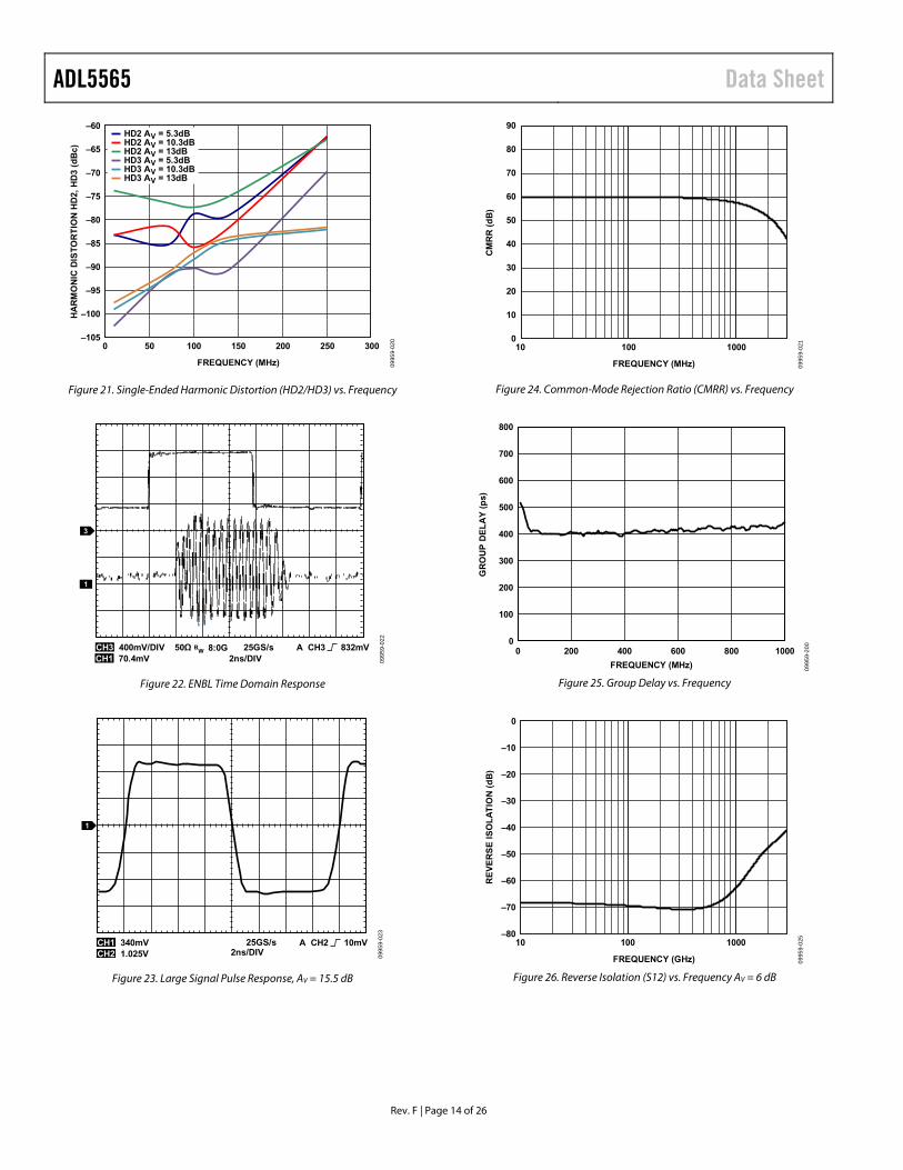
Figure 21. Single-Ended Harmonic Distortion (HD2/HD3) vs. Frequency
CH3 400mV/DIV 25GS/s8:0G A CH3 832mV
1
3
50ΩCH1 70.4mV 2ns/DIV
BW
0995
9-02
2
Figure 22. ENBL Time Domain Response
25GS/sCH1 340mV A CH2 10mV
1
CH2 1.025V 2ns/DIV 0995
9-02
3
Figure 23. Large Signal Pulse Response, AV = 15.5 dB
0
10
20
30
40
50
60
70
80
90
10 100 1000
CM
RR
(d
B)
FREQUENCY (MHz) 0995
9-02
1
Figure 24. Common-Mode Rejection Ratio (CMRR) vs. Frequency
0995
9-20
0
800
0
100
200
300
400
500
600
700
0 200 400 600 800 1000
GR
OU
P D
EL
AY
(p
s)
FREQUENCY (MHz)
Figure 25. Group Delay vs. Frequency
–80
–70
–60
–50
–40
–30
–20
–10
0
10 100 1000
RE
VE
RS
E I
SO
LA
TIO
N (
dB
)
FREQUENCY (GHz) 0995
9-02
5
Figure 26. Reverse Isolation (S12) vs. Frequency AV = 6 dB

Data Sheet ADL5565
Rev. F | Page 15 of 26
0995
9-20
1
300
280
260
240
220
200
180
160
140
120
100
80
60
3.0
2.5
2.0
1.5
1.0
0.5
010 100 1000
EQU
IVA
LEN
T PA
RA
LLEL
INPU
T R
ESIS
TAN
CE
(Ω)
EQU
IVA
LEN
T PA
RA
LLEL
INPU
T C
APA
CIT
AN
CE
(pF)
FREQUENCY (MHz)
RESISTANCE
CAPACITANCE
Figure 27. S11 Equivalent RLC Parallel Network, AV = 6 dB
0995
9-20
220
18
16
14
12
10
8
6
4
2
0
10
1
2
3
4
5
6
7
8
9
010 100 1000
EQU
IVA
LEN
T SE
RIE
S O
UTP
UT
RES
ISTA
NC
E (Ω
)
EQU
IVA
LEN
T SE
RIE
S O
UTP
UT
IND
UC
TAN
CE
(nH
)
FREQUENCY (MHz)
RESISTANCE
CAPACITANCE
Figure 28. S22 Equivalent RLC Parallel Network, AV = 6 dB
60
65
70
75
80
85
–40 –20 0 20 40 60 80 100
I SU
PPLY
(mA
)
TEMPERATURE (°C)
5V
3.3V
0995
9-02
7
Figure 29. ISUPPLY vs. Temperature, RL = 200 Ω, AV = 6 dB,
VPOS = 3.3 V and VPOS = 5 V
ADL5565 Data Sheet
Rev. F | Page 16 of 26
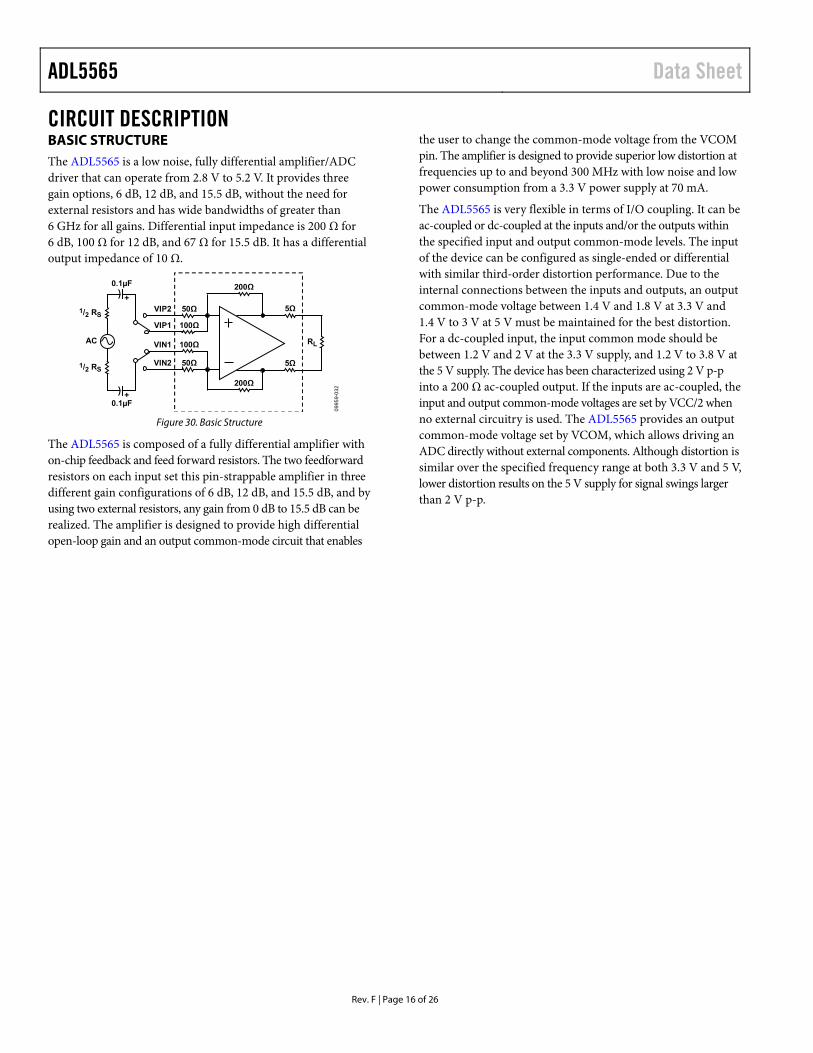
CIRCUIT DESCRIPTION BASIC STRUCTURE The ADL5565 is a low noise, fully differential amplifier/ADC driver that can operate from 2.8 V to 5.2 V. It provides three gain options, 6 dB, 12 dB, and 15.5 dB, without the need for external resistors and has wide bandwidths of greater than 6 GHz for all gains. Differential input impedance is 200 Ω for 6 dB, 100 Ω for 12 dB, and 67 Ω for 15.5 dB. It has a differential output impedance of 10 Ω.
RL
1/2 RS
1/2 RS
AC
100Ω
200Ω0.1µF
0.1µF
200Ω
100Ω
50Ω
50ΩVIP2
VIP1
VIN1
VIN2
5Ω
5Ω
++
0995
9-03
2
Figure 30. Basic Structure
The ADL5565 is composed of a fully differential amplifier with on-chip feedback and feed forward resistors. The two feedforward resistors on each input set this pin-strappable amplifier in three different gain configurations of 6 dB, 12 dB, and 15.5 dB, and by using two external resistors, any gain from 0 dB to 15.5 dB can be realized. The amplifier is designed to provide high differential open-loop gain and an output common-mode circuit that enables
the user to change the common-mode voltage from the VCOM pin. The amplifier is designed to provide superior low distortion at frequencies up to and beyond 300 MHz with low noise and low power consumption from a 3.3 V power supply at 70 mA.
The ADL5565 is very flexible in terms of I/O coupling. It can be ac-coupled or dc-coupled at the inputs and/or the outputs within the specified input and output common-mode levels. The input of the device can be configured as single-ended or differential with similar third-order distortion performance. Due to the internal connections between the inputs and outputs, an output common-mode voltage between 1.4 V and 1.8 V at 3.3 V and 1.4 V to 3 V at 5 V must be maintained for the best distortion. For a dc-coupled input, the input common mode should be between 1.2 V and 2 V at the 3.3 V supply, and 1.2 V to 3.8 V at the 5 V supply. The device has been characterized using 2 V p-p into a 200 Ω ac-coupled output. If the inputs are ac-coupled, the input and output common-mode voltages are set by VCC/2 when no external circuitry is used. The ADL5565 provides an output common-mode voltage set by VCOM, which allows driving an ADC directly without external components. Although distortion is similar over the specified frequency range at both 3.3 V and 5 V, lower distortion results on the 5 V supply for signal swings larger than 2 V p-p.

Data Sheet ADL5565
Rev. F | Page 17 of 26
APPLICATIONS INFORMATION BASIC CONNECTIONS Figure 31 shows the basic connections for operating the ADL5565. Apply a voltage between 3 V and 5 V to the VCC pins, and decouple each supply pin with at least one low inductance, 0.1 µF surface-mount ceramic capacitor, placed as close as possible to the device. Also, decouple the VCOM pin (Pin 9) using a 0.1 µF capacitor.
The gain of the part is determined by the pin-strappable input configuration. When Input A is applied to VIP1 and Input B is applied to VIN1, the gain is 6 dB (minimum gain, see Equation 1 and Equation 2). When Input A is applied to VIP2 and Input B
is applied to VIN2, the gain is 12 dB (middle gain). When Input A is applied to both VIP1 and VIP2 and Input B is applied to both VIN1 and VIN2, the gain is 15.5 dB (maximum gain).
Pin 1 to Pin 4, Pin 10, and Pin 11 are biased at 1/2 VCC above ground and can be dc-coupled (if within the specified input or output common-mode voltage levels) or ac-coupled as shown in Figure 31.
To enable the ADL5565, the ENBL pin must be pulled high. Pulling the ENBL pin low puts the ADL5565 in sleep mode, reducing the current consumption to 5 mA at ambient.
1
2
3
4
11
12
10
9
5 6 7 8
1516 14 13
VIP2
VIP1
VIN1
VIN2
VOP
ENBL
VON
VCOM
VCC VCC VCC
VCC
AC
VCC
GNDGNDGNDGND
ADL5565
VCC
BALANCEDLOADRL
0.1µF 0.1µF
0.1µF
A
B0.1µF
0.1µF0.1µF10µF
0.1µF
RS/2
RS/2
BALANCEDSOURCE
0995
9-03
3
Figure 31. Basic Connections
ADL5565 Data Sheet
Rev. F | Page 18 of 26
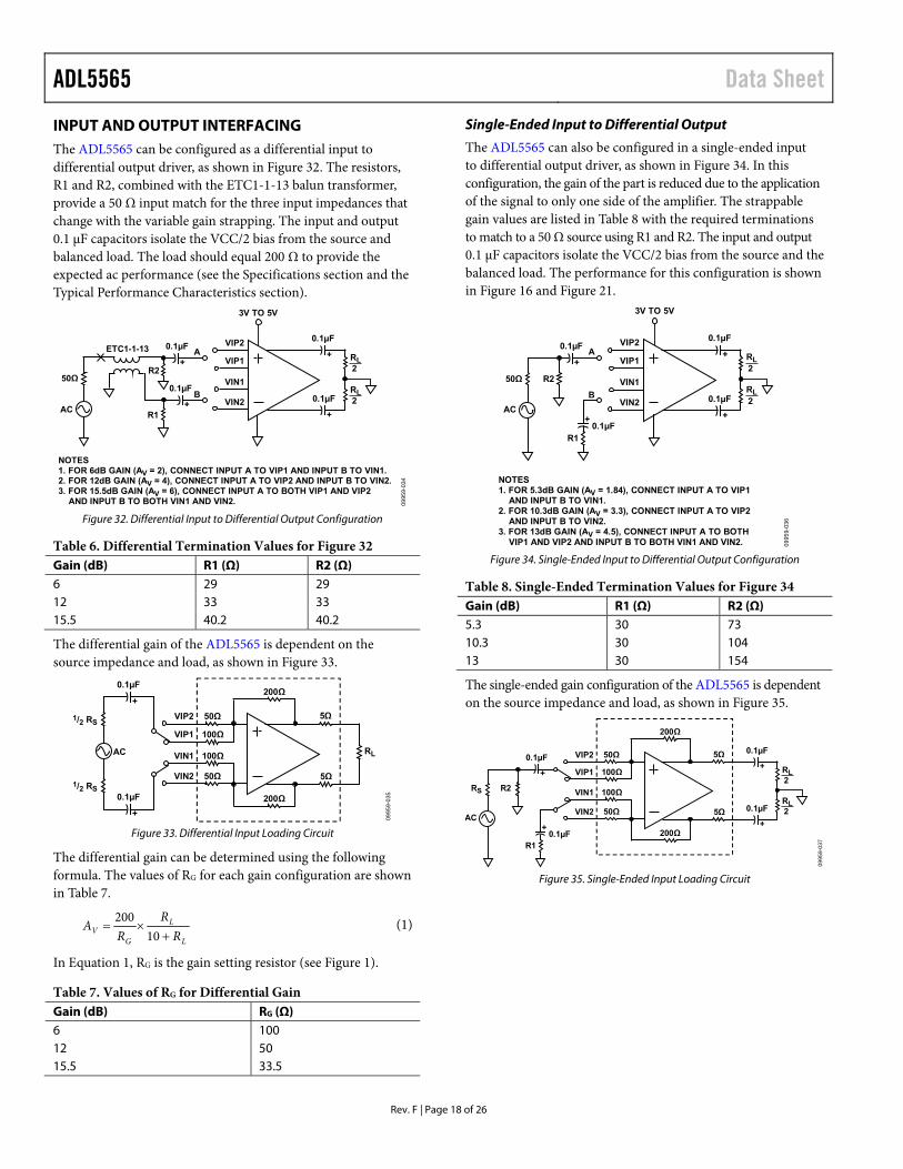
INPUT AND OUTPUT INTERFACING The ADL5565 can be configured as a differential input to differential output driver, as shown in Figure 32. The resistors, R1 and R2, combined with the ETC1-1-13 balun transformer, provide a 50 Ω input match for the three input impedances that change with the variable gain strapping. The input and output 0.1 μF capacitors isolate the VCC/2 bias from the source and balanced load. The load should equal 200 Ω to provide the expected ac performance (see the Specifications section and the Typical Performance Characteristics section).
3V TO 5V
VIP2
VIP1
VIN1
VIN2
A
B
50Ω
AC
R2
++
0.1µF
ETC1-1-130.1µF
+
R1
+
0.1µF
0.1µF
NOTES1. FOR 6dB GAIN (AV = 2), CONNECT INPUT A TO VIP1 AND INPUT B TO VIN1.2. FOR 12dB GAIN (AV = 4), CONNECT INPUT A TO VIP2 AND INPUT B TO VIN2.3. FOR 15.5dB GAIN (AV = 6), CONNECT INPUT A TO BOTH VIP1 AND VIP2 AND INPUT B TO BOTH VIN1 AND VIN2.
RL2
RL2
0995
9-03
4
Figure 32. Differential Input to Differential Output Configuration
Table 6. Differential Termination Values for Figure 32 Gain (dB) R1 (Ω) R2 (Ω) 6 29 29 12 33 33 15.5 40.2 40.2
The differential gain of the ADL5565 is dependent on the source impedance and load, as shown in Figure 33.
100Ω
200Ω
200Ω
100Ω
50Ω
50ΩVIP2
VIP1
VIN1
VIN2
5Ω
5Ω
RLAC
1/2 RS
1/2 RS0.1µF
+
0.1µF
+
0995
9-03
5
Figure 33. Differential Input Loading Circuit
The differential gain can be determined using the following formula. The values of RG for each gain configuration are shown in Table 7.
L
L
GV R
RR
A
10
200 (1)
In Equation 1, RG is the gain setting resistor (see Figure 1).
Table 7. Values of RG for Differential Gain Gain (dB) RG (Ω) 6 100 12 50 15.5 33.5
Single-Ended Input to Differential Output
The ADL5565 can also be configured in a single-ended input to differential output driver, as shown in Figure 34. In this configuration, the gain of the part is reduced due to the application of the signal to only one side of the amplifier. The strappable gain values are listed in Table 8 with the required terminations to match to a 50 Ω source using R1 and R2. The input and output 0.1 μF capacitors isolate the VCC/2 bias from the source and the balanced load. The performance for this configuration is shown in Figure 16 and Figure 21.
VIP2
VIP1
VIN1
VIN2
A
B
50Ω
AC
R2
++
0.1µF
0.1µF
0.1µF
3V TO 5V
+
R1
NOTES1. FOR 5.3dB GAIN (AV = 1.84), CONNECT INPUT A TO VIP1 AND INPUT B TO VIN1.
2. FOR 10.3dB GAIN (AV = 3.3), CONNECT INPUT A TO VIP2 AND INPUT B TO VIN2.
3. FOR 13dB GAIN (AV = 4.5), CONNECT INPUT A TO BOTH VIP1 AND VIP2 AND INPUT B TO BOTH VIN1 AND VIN2.
+
0.1µF
RL2
RL2
0995
9-03
6
Figure 34. Single-Ended Input to Differential Output Configuration
Table 8. Single-Ended Termination Values for Figure 34 Gain (dB) R1 (Ω) R2 (Ω) 5.3 30 73 10.3 30 104 13 30 154
The single-ended gain configuration of the ADL5565 is dependent on the source impedance and load, as shown in Figure 35.
RL
200Ω
200Ω
VIP2
VIP1
VIN1
VIN2
5Ω
5Ω
RS
AC
R2
++
0.1µF
0.1µF
0.1µF0.1µF
+
R1
+
2
RL2
100Ω
100Ω
50Ω
50Ω
0995
9-03
7
Figure 35. Single-Ended Input Loading Circuit

Data Sheet ADL5565
Rev. F | Page 19 of 26
The single-ended gain can be determined using the following formula. The values of RG and RX for each gain configuration are shown in Table 9.
L
L
X
SX
S
S
SG
V RR
RRR
RRR
RRRR
RA
+×
+×
+×
+×
+
=102
2
22
2001 (2)
In Equation 2, RG is the gain setting resistor (see Figure 1).
Table 9. Values of RG and RX for Single-Ended Gain
Gain (dB) RG (Ω)1 RX (Ω) 5.3 100 R2 || 1582 10.3 50 R2 || 962 13 33.5 R2 || 742
1 RG is the gain setting resistor (see Figure 1). 2 These values are based on a 50 Ω input match.
GAIN ADJUSTMENT AND INTERFACING The effective gain of the ADL5565 can be reduced using a number of techniques. A matched attenuator network can reduce the effective gain; however, this requires the addition of a separate component that can be prohibitive in size and cost. Instead, a simple voltage divider can be implemented using the combination of additional series resistors at the amplifier input and the input impedance of the ADL5565, as shown in Figure 36. A pair of resistors is used to match to the impedance of the previous stage.
0.1µF
1/2 RSHUNT
1/2 RS
1/2 RS
AC
0.1µF 1/2 RSERIES
VIP1
VIN2
VIN1
VIP2
1/2 RSERIES
1/2 RSHUNTADL5565
0995
9-03
8
Figure 36. Gain Adjustment Using a Series Resistor
Figure 36 shows a typical implementation of the divider concept that effectively reduces the gain by adding attenuation at the input. For frequencies less than 100 MHz, the input impedance of the ADL5565 can be modeled as a real 66 Ω, 100 Ω, or 200 Ω resistance (differential) for maximum, middle, and minimum gains, respectively. Assuming that the frequency is low enough to ignore the shunt reactance of the input and high enough so that the reactance of moderately sized ac coupling capacitors can be considered negligible, the insertion loss, Il, due to the shunt divider can be expressed as
+=
GSERIES
G
RRR
dBIl log20)( (3)
In Equation 3, RG is the gain setting resistor (see Figure 1).
Adjusted Gain (dB) = 6 dB, 12 dB, or 15.5 dB Gain – Il (dB) (4)
The necessary shunt component, RSHUNT, to match to the source impedance, RS, can be expressed as
GSERIESS
SHUNT
RRR
R
+−
= 111 (5)
In Equation 5, RG is the gain setting resistor (see Figure 1).
The insertion loss and the resultant power gain for multiple shunt resistor values are summarized in Table 10. The source resistance and input impedance need careful attention when using Equation 3, Equation 4, and Equation 5. The reactance of the input impedance of the ADL5565 and the ac coupling capacitors must be considered before assuming that they make a negligible contribution.
Table 10. Differential Gain Adjustment Using Series Resistor Gain (dB)
Differential RG (Ω)4 RS (Ω)
Differential RSERIES (Ω)
Differential RSHUNT (Ω)5
01 200 50 200 57.6 11 200 50 154 57.6 21 200 50 118 59 31 200 50 84.5 60.4 41 200 50 52.3 61.9 51 200 50 24.9 64.9 61 200 50 0 66.5 72 100 50 78.7 69.8 82 100 50 59 73.2 92 100 50 42.2 76.8 102 100 50 26.7 82.5 112 100 50 12.7 88.7 122 100 50 0 100 133 66.7 50 23.7 113 143 66.7 50 13.7 133 15.53 66.7 50 0 200
1 Amplifier is configured for 6 dB gain setting. 2 Amplifier is configured for 12 dB gain setting. 3 Amplifier is configured for 15.5 dB gain setting. 4 RG is the gain setting resistor (see Figure 1). 5 The resistor values are rounded to the nearest real resistor value.
ADL5565 Data Sheet
Rev. F | Page 20 of 26
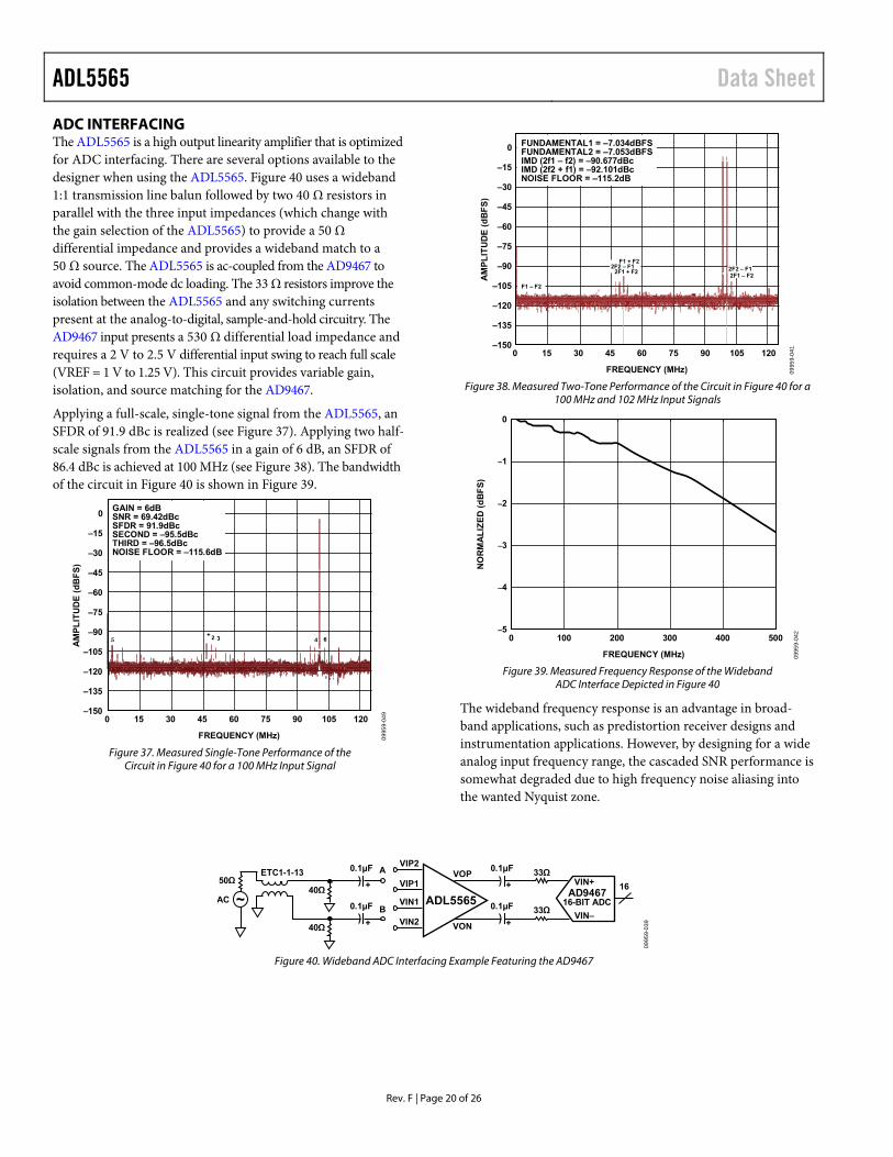
ADC INTERFACING The ADL5565 is a high output linearity amplifier that is optimized for ADC interfacing. There are several options available to the designer when using the ADL5565. Figure 40 uses a wideband 1:1 transmission line balun followed by two 40 Ω resistors in parallel with the three input impedances (which change with the gain selection of the ADL5565) to provide a 50 Ω differential impedance and provides a wideband match to a 50 Ω source. The ADL5565 is ac-coupled from the AD9467 to avoid common-mode dc loading. The 33 Ω resistors improve the isolation between the ADL5565 and any switching currents present at the analog-to-digital, sample-and-hold circuitry. The AD9467 input presents a 530 Ω differential load impedance and requires a 2 V to 2.5 V differential input swing to reach full scale (VREF = 1 V to 1.25 V). This circuit provides variable gain, isolation, and source matching for the AD9467.
Applying a full-scale, single-tone signal from the ADL5565, an SFDR of 91.9 dBc is realized (see Figure 37). Applying two half-scale signals from the ADL5565 in a gain of 6 dB, an SFDR of 86.4 dBc is achieved at 100 MHz (see Figure 38). The bandwidth of the circuit in Figure 40 is shown in Figure 39.
0
150 30 45 60 75 90 105 120
GAIN = 6dBSNR = 69.42dBcSFDR = 91.9dBcSECOND = –95.5dBcTHIRD = –96.5dBcNOISE FLOOR = –115.6dB
AM
PL
ITU
DE
(d
BF
S)
FREQUENCY (MHz)
–15
–30
–45
–60
–75
–90
–105
–120
–135
–150
0995
9-04
9
Figure 37. Measured Single-Tone Performance of the
Circuit in Figure 40 for a 100 MHz Input Signal
2F2 – F12F1 – F2
F1 – F2
2F2 – F12F1 + F2
F1 + F2
0
150 30 45 60 75 90 105 120
FUNDAMENTAL1 = –7.034dBFSFUNDAMENTAL2 = –7.053dBFSIMD (2f1 – f2) = –90.677dBcIMD (2f2 + f1) = –92.101dBcNOISE FLOOR = –115.2dB
AM
PL
ITU
DE
(d
BF
S)
FREQUENCY (MHz)
–15
–30
–45
–60
–75
–90
–105
–120
–135
–150
0995
9-04
1
Figure 38. Measured Two-Tone Performance of the Circuit in Figure 40 for a
100 MHz and 102 MHz Input Signals
–5
–4
–3
–2
–1
0
0 100 200 300 400 500
NO
RM
AL
IZE
D (
dB
FS
)
FREQUENCY (MHz) 0995
9-04
2
Figure 39. Measured Frequency Response of the Wideband
ADC Interface Depicted in Figure 40
The wideband frequency response is an advantage in broad-band applications, such as predistortion receiver designs and instrumentation applications. However, by designing for a wide analog input frequency range, the cascaded SNR performance is somewhat degraded due to high frequency noise aliasing into the wanted Nyquist zone.
0.1µF
40Ω
50Ω
AC
0.1µFETC1-1-13
VIN1
VIP1
VIP2A
BVIN2
40ΩADL5565
++
0.1µF
0.1µF 33ΩVOP
VON
33Ω
++
AD946716-BIT ADC
16VIN+
VIN–
0995
9-03
9
Figure 40. Wideband ADC Interfacing Example Featuring the AD9467
Data Sheet ADL5565
Rev. F | Page 21 of 26
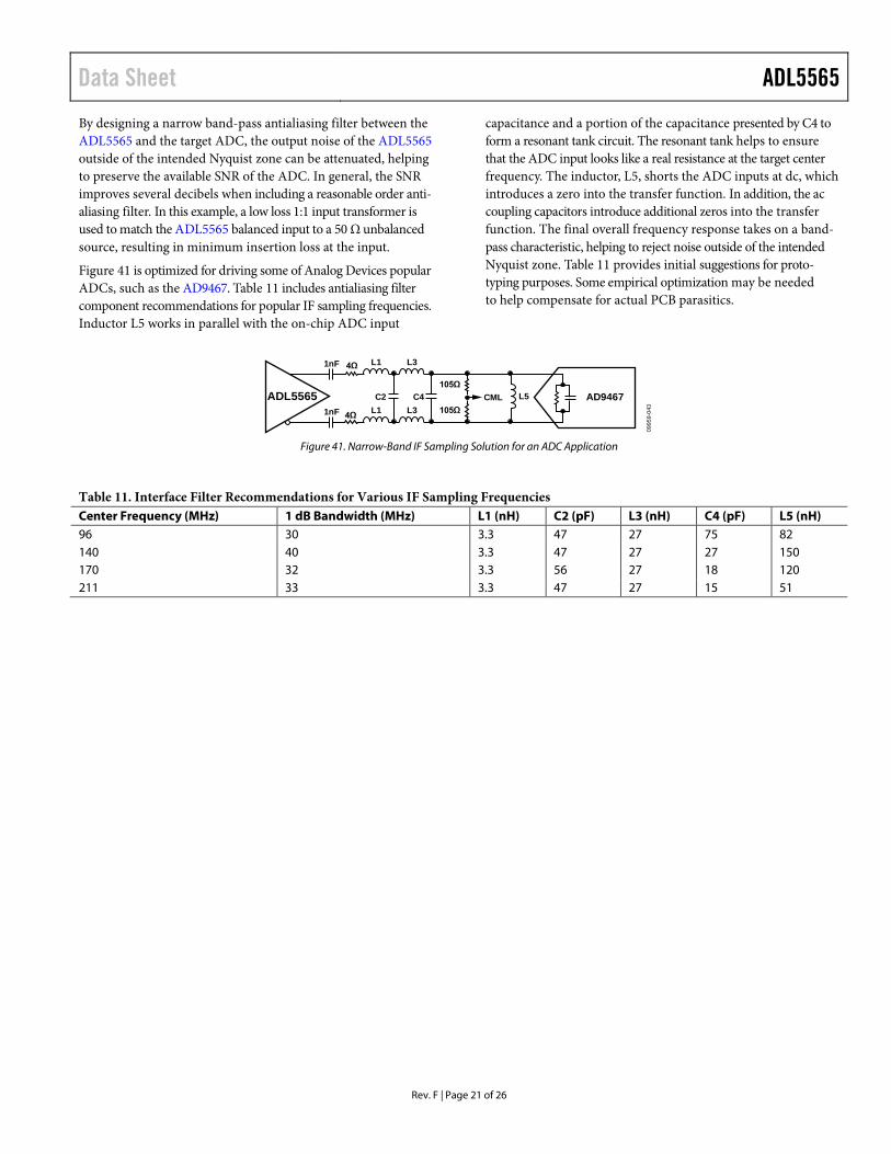
By designing a narrow band-pass antialiasing filter between the ADL5565 and the target ADC, the output noise of the ADL5565 outside of the intended Nyquist zone can be attenuated, helping to preserve the available SNR of the ADC. In general, the SNR improves several decibels when including a reasonable order anti-aliasing filter. In this example, a low loss 1:1 input transformer is used to match the ADL5565 balanced input to a 50 Ω unbalanced source, resulting in minimum insertion loss at the input.
Figure 41 is optimized for driving some of Analog Devices popular ADCs, such as the AD9467. Table 11 includes antialiasing filter component recommendations for popular IF sampling frequencies. Inductor L5 works in parallel with the on-chip ADC input
capacitance and a portion of the capacitance presented by C4 to form a resonant tank circuit. The resonant tank helps to ensure that the ADC input looks like a real resistance at the target center frequency. The inductor, L5, shorts the ADC inputs at dc, which introduces a zero into the transfer function. In addition, the ac coupling capacitors introduce additional zeros into the transfer function. The final overall frequency response takes on a band-pass characteristic, helping to reject noise outside of the intended Nyquist zone. Table 11 provides initial suggestions for proto-typing purposes. Some empirical optimization may be needed to help compensate for actual PCB parasitics.
105ΩL5
105ΩAD9467
1nF L1
C2
L3
1nF L1 L3C4 CMLADL5565
4Ω
4Ω
0995
9-04
3
Figure 41. Narrow-Band IF Sampling Solution for an ADC Application
Table 11. Interface Filter Recommendations for Various IF Sampling Frequencies Center Frequency (MHz) 1 dB Bandwidth (MHz) L1 (nH) C2 (pF) L3 (nH) C4 (pF) L5 (nH) 96 30 3.3 47 27 75 82 140 40 3.3 47 27 27 150 170 32 3.3 56 27 18 120 211 33 3.3 47 27 15 51
ADL5565 Data Sheet
Rev. F | Page 22 of 26
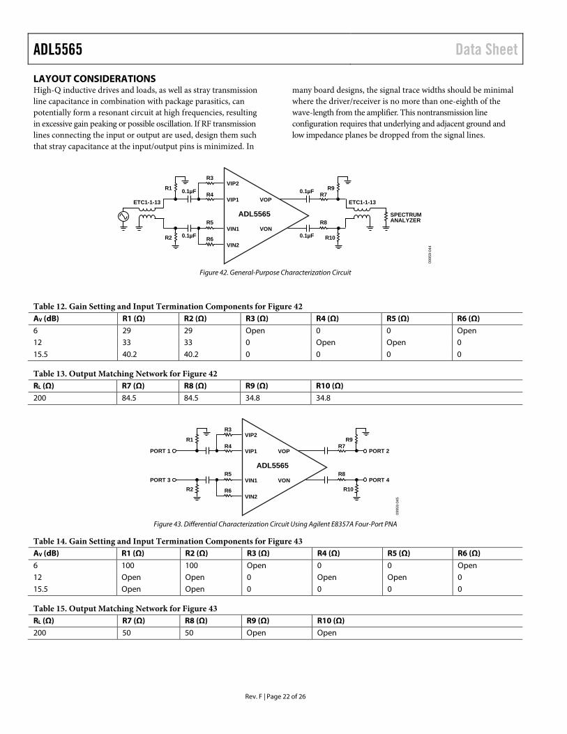
LAYOUT CONSIDERATIONS High-Q inductive drives and loads, as well as stray transmission line capacitance in combination with package parasitics, can potentially form a resonant circuit at high frequencies, resulting in excessive gain peaking or possible oscillation. If RF transmission lines connecting the input or output are used, design them such that stray capacitance at the input/output pins is minimized. In
many board designs, the signal trace widths should be minimal where the driver/receiver is no more than one-eighth of the wave-length from the amplifier. This nontransmission line configuration requires that underlying and adjacent ground and low impedance planes be dropped from the signal lines.
0.1µF
0.1µF
0.1µF
0.1µF
ADL5565
VIP2
VIP1
VIN1
VOP
VON
VIN2R6
R5
R4
R3
R2
R1
R8
R7
R10
R9
ETC1-1-13 ETC1-1-13
SPECTRUMANALYZER
0995
9-04
4
Figure 42. General-Purpose Characterization Circuit
Table 12. Gain Setting and Input Termination Components for Figure 42 AV (dB) R1 (Ω) R2 (Ω) R3 (Ω) R4 (Ω) R5 (Ω) R6 (Ω)
6 29 29 Open 0 0 Open 12 33 33 0 Open Open 0
15.5 40.2 40.2 0 0 0 0
Table 13. Output Matching Network for Figure 42 RL (Ω) R7 (Ω) R8 (Ω) R9 (Ω) R10 (Ω)
200 84.5 84.5 34.8 34.8
ADL5565
VIP2
VIP1
VIN1
VOP
VON
VIN2R6
R5
R4
R3
R2
R1
PORT 1
PORT 3
PORT 2
PORT 4R8
R7
R10
R9
0995
9-04
5
Figure 43. Differential Characterization Circuit Using Agilent E8357A Four-Port PNA
Table 14. Gain Setting and Input Termination Components for Figure 43 AV (dB) R1 (Ω) R2 (Ω) R3 (Ω) R4 (Ω) R5 (Ω) R6 (Ω)
6 100 100 Open 0 0 Open 12 Open Open 0 Open Open 0 15.5 Open Open 0 0 0 0
Table 15. Output Matching Network for Figure 43 RL (Ω) R7 (Ω) R8 (Ω) R9 (Ω) R10 (Ω)
200 50 50 Open Open

Data Sheet ADL5565
Rev. F | Page 23 of 26
SOLDERING INFORMATION AND RECOMMENDED PCB LAND PATTERN Figure 44 shows the recommended land pattern for the ADL5565. The ADL5565 is contained in a 3 × 3 mm LFCSP package, which has an exposed ground paddle (EPAD). This paddle is internally connected to the ground of the chip. To minimize thermal impedance and ensure electrical performance, solder the paddle to the low impedance ground plane on the PCB. To further reduce thermal impedance, it is recommended that the ground planes on all layers under the paddle be stitched together with vias.
For more information on land pattern design and layout, refer to the AN-772 Application Note, A Design and Manufacturing Guide for the Lead Frame Chip Scale Package (LFCSP).
This land pattern, on the ADL5565 evaluation board, provides a measured thermal resistance (θJA) of 60°C/W. To measure θJA, the temperature at the top of the LFCSP package is found with an IR temperature gun. Thermal simulation suggests a junction temperature 1.5°C higher than the top of package temperature. With additional ambient temperature and I/O power measure-ments, θJA could be determined.
36mils
12m
ils
59m
ils
59m
ils
122m
ils
19.7mils
10mils
0995
9-05
0
59mils
Figure 44. Recommended Land Pattern
EVALUATION BOARD Figure 45 shows the schematic of the ADL5565 evaluation board. The board is powered by a single supply in the 3 V to 5 V range. The power supply is decoupled by 10 µF and 0.1 µF capacitors.
Table 16 details the various configuration options of the evaluation board. Figure 46 and Figure 47 show the component and circuit side layouts of the evaluation board.
To realize the minimum gain (6 dB into a 200 Ω load), Input 1 (VIN1 and VIP1) must be used by installing 0 Ω resistors at R3 and R4, leaving R5 and R6 open. R1 and R2 must be 33.2 Ω for a 50 Ω input impedance.
Likewise, driving Input 2 (VIN2 and VIP2) realizes the middle gain (12 dB into a 200 Ω load) by installing 0 Ω at R5 and R6 and leaving R3 and R4 open. R1 and R2 must be 50 Ω for a 50 Ω input impedance.
For the maximum gain (15.5 dB into a 200 Ω load), both inputs are driven by installing 0 Ω resistors at R3, R4, R5, and R6. R1 and R2 are open for a 50 Ω input impedance.
The balanced input and output interfaces are converted to single ended with a pair of baluns (M/A-COM ETC1-1-13). The balun at the input, T1, provides a 50 Ω single-ended-to-differential transformation. The output balun, T2, and the matching components are configured to provide a 200 Ω to 50 Ω impedance transformation with an insertion loss of about 11 dB.
As an alternative, the input transformer, T1, can be replaced with one of the following transformers to provide a low loss balanced input to the ADL5565.
• 6 dB gain configuration, Mini-Circuits TC4-1W+ • 12 dB gain configuration, Mini-Circuits, TC2-1T+ • 15.5 dB gain configuration, Mini-Circuits TC1.5-52T
When using these alternative transformers, R1 and R2 are left open. Replace C1 and C2 with 0 Ω jumpers and add a 0.1 µF capacitor to C12.

ADL5565 Data Sheet
Rev. F | Page 24 of 26
C310µF
C40.1µF
C50.1µF
C60.1µF
C70.1µF
C80.1µF
C13OPEN
C110.1µF
VPOS
R934.8Ω
R11OPEN
R15OPEN
R140Ω
J3
R1034.8Ω
R884.5ΩC10
0.01µF
C90.01µF
P1
T2
VCOM
AGND
VPOS
GND
R784.5Ω
ENBL
J4OPEN
R12OPEN
R130Ω
J2OPEN
ADL5565
9
10
11
12
4
3
2
1
16 15 14 13
5 6 7 8
GND GND GND GND
VCC
VIN1
VIN2
VIP2
VIP1
VON
VCOM
ENBL
VOP
VCC VCC VCC
C12OPEN
J1T1
R1OPEN
R2OPEN
R40Ω
R30Ω
R50Ω
R60Ω
C10.01µF
C20.01µF
0995
9-04
6
Figure 45. Evaluation Board Schematic
Table 16. Evaluation Board Configuration Options Component Description Default Condition VPOS, GND Ground and supply vector pins. VPOS, GND = installed C3, C4, C5, C6, C7, C11
Power supply decoupling. The supply decoupling consists of a 10 µF capacitor (C3) to ground. C4 to C7 are bypass capacitors. C11 ac couples VREF to ground.
C3 = 10 µF (Size D), C4, C5, C6, C7, C11 = 0.1 µF (Size 0402)
J1, J2, R1, R2, R3, R4, R5, R6, R12, R13, C1, C2, C12, T1
Input interface. The SMA labeled J1 is the input. T1 is a 1-to-1 impedance ratio balun to transform a single-ended input into a balanced differential signal. Removing R13, installing R12 (0 Ω), and installing an SMA connector (J2) allows driving from a differential source. C1 and C2 provide ac coupling. C12 is a bypass capacitor. R1 and R2 provide a differential 50 Ω input termination. R3 to R6 are used to select the input for the pin-strappable gain. The maximum gain is R3, R4, R5, R6 = 0 Ω and R1 and R2 = open. The middle gain is R5 and R6 = 0 Ω, R3 and R4 = open, and R1 and R2 = 50 Ω. The minimum gain is R3 and R4 = 0 Ω, R5 and R6 = open, and R1 and R2 = 33.2 Ω.
J1 = installed, J2 = not installed, R1, R2 = open, R3, R4, R5, R6, R13 = 0 Ω (Size 0402), R12, = open, C1, C2 = 0.01 µF (Size 0402), C12 = open, T1 = ETC1-1-13 (M/A-COM)
J3, J4, R7, R8, R9, R10, R11, R14, R15 C9, C10, C13, T2
Output interface. The SMA labeled J3 is the output. T2 is a 1-to-1 impedance ratio balun to transform a balanced differential signal to a single-ended signal. Removing R14, installing R15 (0 Ω), and installing an SMA connector (J4) allows differential loading. C13 is a bypass capacitor. R7, R8, R9, and R10 are provided for generic placement of matching components. The evaluation board is configured to provide a 200 Ω to 50 Ω impedance transformation with an insertion loss of 17 dB. C9 and C10 provide ac coupling.
J3 = installed, J4 = not installed, R7, R8 = 84.5 Ω (Size 0402), R9, R10 = 34.8 Ω (Size 0402), R11, R15 = open (Size 0402), R14 = 0 Ω (Size 0402) C9, C10 = 0.01 µF (Size 0402), C13 = open T2 = ETC1-1-13 (M/A-COM)
ENBL, P1, C8 Device enabled. C8 is a bypass capacitor. When the P1 jumper is set toward the VPOS label, the ENBL pin is connected to the supply, enabling the device. In the opposite direction, toward the GND label, the ENBL pin is grounded, putting the device in power-down mode.
ENBL, P1 = installed, C8 = 0.1 µF (Size 0402)
Table 17. Differential Values for Figure 45 Gain (dB) R1 (Ω) R2 (Ω) 6 29 29 12 33 33 15.5 Open Open
Table 18. Alternative Differential Input Configuration for Figure 45 Gain (dB) R1 and R2 (Ω) C12 (µF) C1 and C2 (Ω) T1 6 Open 0.1 0 Mini Circuits TC4-1W+ 12 Open 0.1 0 Mini Circuits TC2-1T+ 15.5 Open 0.1 0 Mini Circuits TC1.5-52T+
Data Sheet ADL5565
Rev. F | Page 25 of 26
0995
9-04
7
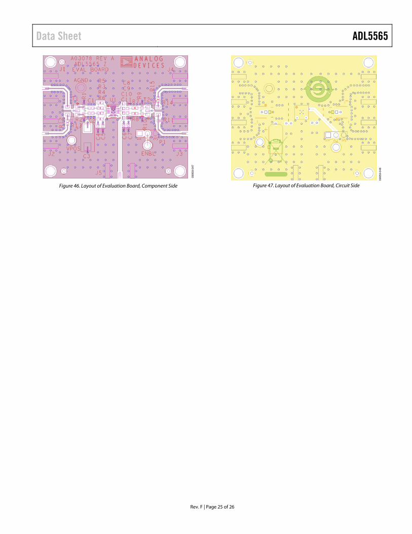
Figure 46. Layout of Evaluation Board, Component Side
0995
9-04
8
Figure 47. Layout of Evaluation Board, Circuit Side

ADL5565 Data Sheet
Rev. F | Page 26 of 26
OUTLINE DIMENSIONS 0.300.230.18
1.751.60 SQ1.45
3.103.00 SQ2.90
10.50BSC
BOTTOM VIEWTOP VIEW
16
58
9
12
13
4
0.500.400.30
0.05 MAX0.02 NOM
0.20 REF
0.20 MIN
COPLANARITY0.08
PIN 1INDICATOR
0.800.750.70
COMPLIANT TOJEDEC STANDARDS MO-220-WEED-6.PKG
-005
138
SEATINGPLANE
SIDE VIEW
EXPOSEDPAD
02-2
3-20
17-E
PIN 1INDICATOR AREA OPTIONS(SEE DETAIL A)
DETAIL A(JEDEC 95)
FOR PROPER CONNECTION OFTHE EXPOSED PAD, REFER TOTHE PIN CONFIGURATION ANDFUNCTION DESCRIPTIONSSECTION OF THIS DATA SHEET.
Figure 48. 16-Lead Lead Frame Chip Scale Package [LFCSP]
3 mm × 3 mm Body and 0.75 mm Package Height (CP-16-22)
Dimensions shown in millimeters
ORDERING GUIDE
Model1 Temperature Range Package Description
Package Option Branding
ADL5565ACPZ-R7 −40°C to + 85°C 16-Lead Lead Frame Chip Scale Package [LFCSP], 7” Tape and Reel CP-16-22 Q1Z ADL5565-EVALZ Evaluation Board 1 Z = RoHS Compliant Part
©2011–2017 Analog Devices, Inc. All rights reserved. Trademarks and registered trademarks are the property of their respective owners. D09959-0-11/17(F)