6 EVOLUTION OF MSP430 FAMILY MICROCONTROLLERS...
19
55 CHAPTER - 6 EVOLUTION OF MSP430 FAMILY MICROCONTROLLERS Table of Contents S.No. Name of the sub-title Page No. 6.1 Introduction 60-62 6.2 Architectural features 62-65 6.2.1. Operating Modes 66-69 6.2.2. Principles for Low-power Applications 70 6.2.3. Peripherals 70-73 6.3 Electrical Characteristics 73-77
Transcript of 6 EVOLUTION OF MSP430 FAMILY MICROCONTROLLERS...

55
CHAPTER - 6
EVOLUTION OF MSP430 FAMILY MICROCONTROLLERS
Table of Contents
S.No. Name of the sub-title Page No.
6.1 Introduction 60-62
6.2 Architectural features 62-65
6.2.1. Operating Modes 66-69
6.2.2. Principles for Low-power Applications 70
6.2.3. Peripherals 70-73
6.3 Electrical Characteristics 73-77

56
6. EVOLUTION OF MSP430 FAMILY
MICROCONTROLLERS
6.1 Introduction
MSP430 microcontrollers are 16-bit; RISC based mixed signal
processors from Texas Instruments. These MCUs offer the lowest
power consumption and the perfect mix of integrated peripherals for
thousands of applications. Now-a-days, the complex system design for
various applications of diverse fields, like biomedical engineering
energy consumption is one of the critical design parameter. Similarly,
it needs much effort to achieve low power dissipation in all levels of
design process. The component and sub systems, where operation
requires low power will be chosen for the entire low power design
architecture. To address these critical questions, the TI has come up
with this ultra low power family of microcontrollers which have rich
features for low power system design. It is the platform of very low
power processors with high integration, which can be employed in
several applications like spirometers, pulse oximeters, blood pressure
monitors and heartbeat monitors. This MSP430 microcontroller was
introduced in late 1990s, which is a straightforward 16-bit processor
with Von Neumann architecture and was designed for low power
applications [47]. The MSP indicates that this is equally employed for
both analog and digital signal inputs. For this an ADC with a
resolution of 16-bits is employed.
57
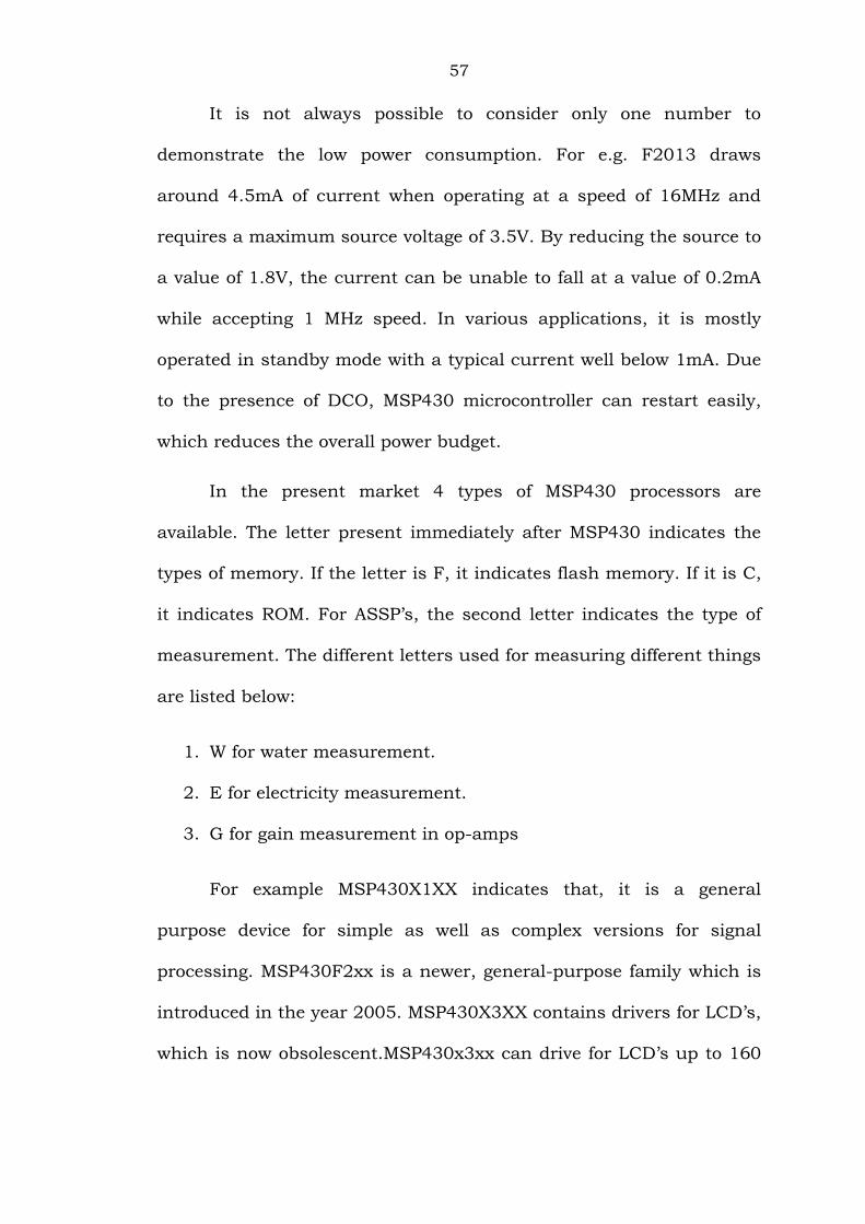
It is not always possible to consider only one number to
demonstrate the low power consumption. For e.g. F2013 draws
around 4.5mA of current when operating at a speed of 16MHz and
requires a maximum source voltage of 3.5V. By reducing the source to
a value of 1.8V, the current can be unable to fall at a value of 0.2mA
while accepting 1 MHz speed. In various applications, it is mostly
operated in standby mode with a typical current well below 1mA. Due
to the presence of DCO, MSP430 microcontroller can restart easily,
which reduces the overall power budget.
In the present market 4 types of MSP430 processors are
available. The letter present immediately after MSP430 indicates the
types of memory. If the letter is F, it indicates flash memory. If it is C,
it indicates ROM. For ASSP’s, the second letter indicates the type of
measurement. The different letters used for measuring different things
are listed below:
1. W for water measurement.
2. E for electricity measurement.
3. G for gain measurement in op-amps
For example MSP430X1XX indicates that, it is a general
purpose device for simple as well as complex versions for signal
processing. MSP430F2xx is a newer, general-purpose family which is
introduced in the year 2005. MSP430X3XX contains drivers for LCD’s,
which is now obsolescent.MSP430x3xx can drive for LCD’s up to 160

58
segments. Many of them are ASSP’s and some of them are general
devices too.
In the present design the MSP430F1611 Microcontroller is used.
The preceding sections will discuss the architectural and other
significant features of this microcontroller.
6.2 Architectural Features
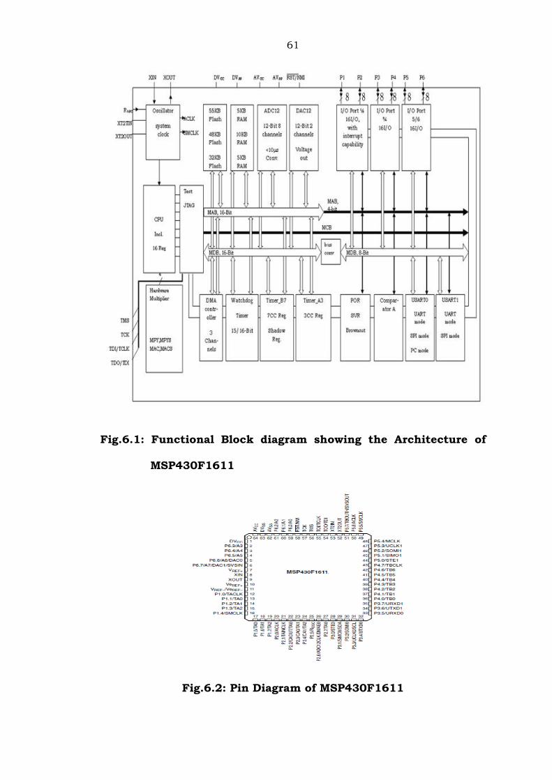
MSP430 controller consists of a 16-bit RISC CPU, clocking
devices and some other peripherals which are interconnected by a
Von-Neumann memory address bus (MAB) and memory data bus
(MDB). By inter connecting a modern CPU with memory mapped
analog, digital devices, it offers the feasibility of mixed-signal
processing. For portable applications, to increase the life of battery
this controller is combined with five low power modes. Maximum code
efficiency is obtained because of very powerful 16-bit RISC CPU, 16-
bit registers, constant generators etc. The DCO offers switching
between different modes with in 6µs interval. The architectural
features of MSP430 micro controller are shown in figure 6.1 and the
pin diagram of MSP430F1611 is shown in figure 6.2.
59
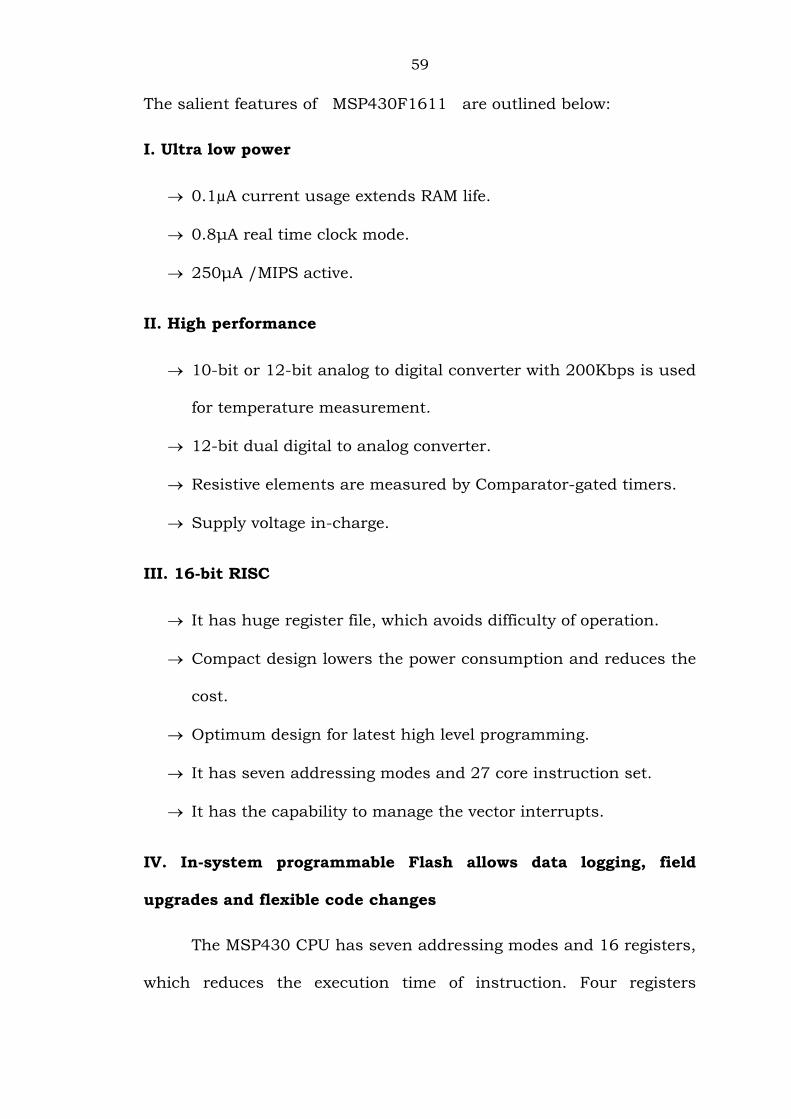
The salient features of MSP430F1611 are outlined below:
I. Ultra low power
0.1µA current usage extends RAM life.
0.8μA real time clock mode.
250μA /MIPS active.
II. High performance
10-bit or 12-bit analog to digital converter with 200Kbps is used
for temperature measurement.
12-bit dual digital to analog converter.
Resistive elements are measured by Comparator-gated timers.
Supply voltage in-charge.
III. 16-bit RISC
It has huge register file, which avoids difficulty of operation.
Compact design lowers the power consumption and reduces the
cost.
Optimum design for latest high level programming.
It has seven addressing modes and 27 core instruction set.
It has the capability to manage the vector interrupts.
IV. In-system programmable Flash allows data logging, field
upgrades and flexible code changes
The MSP430 CPU has seven addressing modes and 16 registers,
which reduces the execution time of instruction. Four registers
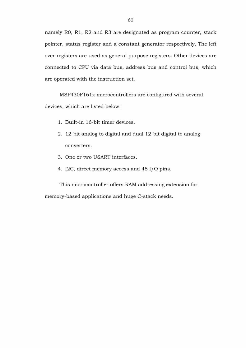
60
namely R0, R1, R2 and R3 are designated as program counter, stack
pointer, status register and a constant generator respectively. The left
over registers are used as general purpose registers. Other devices are
connected to CPU via data bus, address bus and control bus, which
are operated with the instruction set.
MSP430F161x microcontrollers are configured with several
devices, which are listed below:
1. Built-in 16-bit timer devices.
2. 12-bit analog to digital and dual 12-bit digital to analog
converters.
3. One or two USART interfaces.
4. I2C, direct memory access and 48 I/O pins.
This microcontroller offers RAM addressing extension for
memory-based applications and huge C-stack needs.
61
Fig.6.1: Functional Block diagram showing the Architecture of
MSP430F1611
Fig.6.2: Pin Diagram of MSP430F1611

62
6.2.1 Operating Modes
The MSP430 microcontroller has totally six modes of operation.
Among them one is active mode and other five are low-power modes
which are software selectable. Any device can be made to wake-up
from one of these five low-power modes. The six operating modes
which are configured are given below:
I. Active mode AM
In Active mode, all clock cycles are active and power consumption
will be high.
II. Low-power mode 0 (LPM0)
In this mode, the CPU is actually disabled and ACLK and SMCLK
signals are activated at the same time. MCLK is disabled.
III. Low-power mode 1 (LPM1)
In this mode also, CPU is disabled and the ACLK and SMCLK
signals are activated at the same instant. MCLK is disabled and if
DCO is not operated in active manner, it can also be disabled.
IV. Low-power mode 2 (LPM2)
In this mode CPU is disabled, MCLK & SMCLK are disabled. DCO’s
dc generator remains enable & ACLK remains in active mode.
V. Low-power mode 3 (LPM3)
In this mode CPU, MCLK and SMCLK and DCO’s dc generators are
disabled and ACLK signal is activated.
63
VI. Low-power mode 4 (LPM4)
In this fourth mode CPU, ACLK, MCLK, SMCLK and DCO’s dc
generators are disabled.
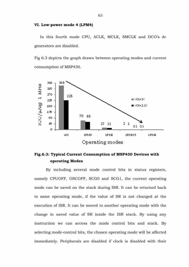
Fig 6.3 depicts the graph drawn between operating modes and current
consumption of MSP430.
Fig.6.3: Typical Current Consumption of MSP430 Devices with
operating Modes
By including several mode control bits in status registers,
namely CPUOFF, OSCOFF, SCG0 and SCG1, the current operating
mode can be saved on the stack during ISR. It can be returned back
to same operating mode, if the value of SR is not changed at the
execution of ISR. It can be moved to another operating mode with the
change in saved value of SR inside the ISR stack. By using any
instruction we can access the mode control bits and stack. By
selecting mode-control bits, the chosen operating mode will be affected
immediately. Peripherals are disabled if clock is disabled with their

64
individual control register settings. All I/O port pins & RAM /registers
remain constant. Wakeup is possible along all enabled interrupts.
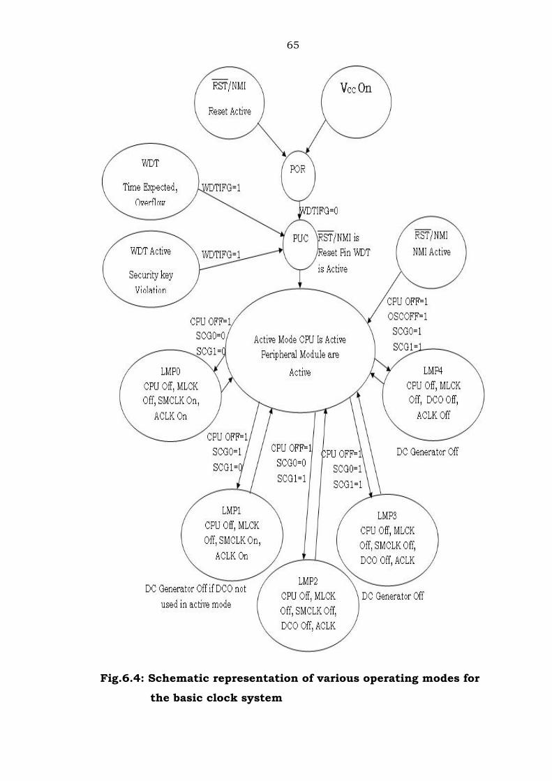
The schematic representation of various operating modes for the
basic clock system is shown in Figure 6.4. From the schematic, it is
clear that in active mode, the CPU is active and all enabled clocks are
active. Whereas in low power mode 4, CPU and all the clocks are
disabled. Hence this mode is the lowest power mode.
65
Fig.6.4: Schematic representation of various operating modes for
the basic clock system

66
6.2.2 Principles for Low-Power Applications
To reduce the power utilization of MSP430, clock system is used
to increase the time period of LPM3 operating mode. The LPM3
requires very less power about 2µA and all interrupts are active. For
activating ACLK and CPU it uses a 32 KHz crystal oscillator clock.
The flow of program can be controlled and the processor can be
made active with the help of interrupts.
The switching of peripheral devices can be done whenever it is
needed.
Fast look-up tables and branching are employed instead of flag
polling and huge software computations.
Because of overhead, unnecessary function calling and frequent
usage of code can be avoided.
Unique CPU register cycles are employed for more usage of long
software subroutines.
6.2.3 Peripherals
The MSP430 microcontroller has a rich set of peripherals. These
peripherals are connected to the CPU through address, data & control
buses and can be handled using all instructions.
I. DMA controller
Direct memory addressing avoids the involvement of CPU in
the process of transferring information from one address to
another address inside the memory. In this case, CPU is kept in

67
sleep mode and avoids unnecessary power consumption. Using
DMA, the throughput of a peripheral device can be increased.
II. Oscillator and system clock
The clocking system of MSP430F1611 series are supported
through clock modules which includes high-frequency crystal
oscillators, a 32768 Hz crystal oscillator and an internal DCO
generator. This clock system is especially applicable to battery
powered applications.
III. Brownout, Supply Voltage Supervisor (SVS)
Proper internal reset signaling can be made at the time of
power on & power off by using a brownout circuit. The supply
voltage supervisor continuously monitors the supply voltage.
When it drops lower than a user required level, the CPU starts
executing the code after resetting the device by employing
brownout circuit clock.
IV. Digital I/O
It has 6 ports designated as P1 to P6, each of them are of 8-
bit length. All the I/O ports are programmed individually. The
ports P1 & P2 offers the feasibility to select Edge interrupts.
V. Watchdog timer
A watchdog timer can be employed to restart a controlled
system after the occurrence of a software problem. The

68
watchdog timer can be used for generating interrupts at
prescribed intervals.
VI. Hardware multiplier
A particular peripheral module can be employed to perform
multiplication operations. This module supports 8x8, 8x16,
16x8 and 16x16 bit multiplication. This module supports signed
& unsigned multiplication, division and accumulation of data.
The result can be immediately obtained after loading the data
into the registers. No extra clocking signals are needed.
VII. USART0 & USART1
These are two hardware modules used by MSP430F1611 to
perform serial data communication. Both of them support SPF,
I2C protocols and UART by employing double buffered
transmitting and receiving channels. They also support
addressing modes of 7-bit and 10-bit with master and slave mode
configuration. To increase throughput of a system 16-bit length
I2C data transfer mode with two dedicated DMA channels are
supported by USART0 and USART1
VIII. Timer_A3
It is a 16-bit counter or timer with 3 compare or capture
registers and supports numerous compare/captures, pulse width
modulated outputs and timing interval. During overflow condition,
each of compare or capture registers generate the interrupts.
69
IX. Timer_B7
It is a 16-bit timer/counter with 7 capture or compare
registers and supports multiple capture/compares, interval timing
etc.
X. Comparator_A
It is particularly meant for supervision of battery voltage,
external analog signal monitoring, precise conversion from analog
to digital.
XI. ADC12
It supports very fast conversion of 12-bit data from analog-to-
digital. It is used to implement 12-bit SAR, sample control,
conversion & control for conversion of 16-bit words and for
generating refresh control signals.
XII. DAC12
It is a 12-bit voltage output DAC, R-ladder. It can be used
for 8-bit or 12-bit operations along with DMA. With DAC12
module, synchronous operations are performed by grouping
them.
6.3 Electrical Characteristics
Most MSP430 devices operate at 1.8 V to 3.6 V, so a typical 3V
supply is enough for proper functioning. Connecting the JTAG to
support device memory programming and debugging is also

70
important. For majority of the devices, there are two possibilities:
standard four-wire JTAG or MSP430 MCU-specific Spy-Bi-Wire (SBW,
or two-wire JTAG). Both interfaces are acceptable for programming
and debugging the application code. The main advantage of the four-
wire mode is speed. The main advantage of the two-wire SBW mode is
reduced pin-connection requirements.
So, to understand the low power activities of this controller, the
electrical characteristics are always useful. The Figure 6.5 shows the
variation of the supply voltage range with the frequency during the
program execution and flash memory programming.
Fig.6.5: Voltage range with the frequency during the program
execution and flash memory programming

71
The utilization of current in active mode with respect to
frequency can be found using following equation:
I (AM) = I (AM) [1MHz] * f (system) [MHz]
The utilization of current in active mode with respect to supply
voltage can be found using following equation:
I (AM) = I (AM) [3V] +210µA/V * (VCC-3v)
Fig 6.6 and 6.7 shows the low-level output characteristics
between voltage & current
Fig.6.6: Typical lowlevel output
voltage vs lowlevel output
current characteristics for
Vcc=2.2V
Fig.6.7: Typical lowlevel output
voltage vs lowlevel output
current characteristics for
Vcc=3V

72
The curves indicate that the output current levels saturate for the Port
3.5 at an output voltage of 2 to 3 volts. It is also observable that with
increase in the voltage levels of Vcc, the saturation levels also changes.
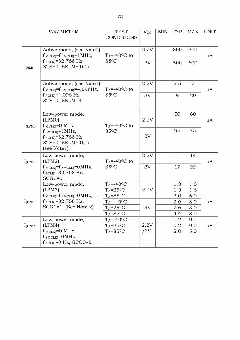
The typical power consumption values for various low-power modes
are shown in the Table 6.1. From the Table it is clear that even in the worst
case of active mode for Vcc =3 V, the maximum power dissipation is around
600µA and the power dissipation for the low power mode 4 is only about 0.5
µA which is considered to be the lowest power consumption of the
microcontroller. But on average one can expect a minimum power
consumption of about 50µA of current only. This is reasonably good for
many biomedical and wires sensor applications. The leakage currents of the
Ports P1 to P6 are also very low with a maximum value of 50 ± nA.
Table 6.1: The typical power consumption values for various low-power
modes
73
PARAMETER TEST
CONDITIONS
VCC MIN TYP MAX UNIT
I(AM)
Active mode, (see Note1) f(MCLK)=f(SMCLK)=1MHz,
f(ACLK)=32,768 Hz XTS=0, SELM=(0.1)
TA=-400C to
850C
2.2V 300 300
A
3V 500 600
Active mode, (see Note1) f(MCLK)=f(SMCLK)=4,096Hz,
f(ACLK)=4,096 Hz XTS=0, SELM=3
TA=-400C to
850C
2.2V 2.5 7
A
3V 9 20
I(LPM0)
Low-power mode, (LPM0) f(MCLK)=0 MHz,
f(SMCLK)=1MHz, f(ACLK)=32,768 Hz XTS=0, SELM=(0,1)
(see Note1)
TA=-400C to
850C
2.2V
50 60
A
3V
95 75
I(LPM2)
Low-power mode, (LPM2) f(MCLK)=f(SMCLK)=0MHz,
f(ACLK)=32,768 Hz, SCG0=0
TA=-400C to 850C
2.2V 11 14
A 3V 17 22
I(LPM3)
Low-power mode, (LPM3) f(MCLK)=f(SMCLK)=0MHz,
f(ACLK)=32,768 Hz, SCG0=1. (See Note 2)
TA=-400C 2.2V
1.3 1.6
A
TA=250C 1.3 1.6
TA=850C 3.0 6.0
TA=-400C
3V
2.6 3.0
TA=250C 2.6 3.0
TA=850C 4.4 8.0
I(LPM4)
Low-power mode, (LPM4)
f(MCLK)=0 MHz, f(SMCLK)=0MHz, f(ACLK)=0 Hz, SCG0=0
TA=-400C 2.2V
/3V
0.2 0.5
A TA=250C 0.2 0.5
TA=850C 2.0 5.0