5.Broadband.vcos 1449
26
Chapter 5 BROADBAND VCOs: CIRCUIT DESIGN CONSIDERATIONS This cha pter de al s with circuit des ign consider ations for broadband RF CMOS VCOs as well as VCO implementation in fully integrated transceiver solutions. RF VCO with subbands is conside red for broadband impleme ntation. Discrete and continuous tuning schemes for broadband VCOs are explored in details. Capacita nce and induc tance switch ing techniques for discrete tuni ng control are evaluated for performance and implementation considerations. Both the active circuit and resonator tank design for RF VCO design are overviewed. Bias circu it is a majo r noise cont ribu tor to the VCO phase noise. Bias filt ering tec hniques are investig ated. Dynamic bias filtering solutions are pre sented for fast VCO start-u p. Passive components forming the LC tank of the VCO are of paramount importance since they mainly determine noise performa nce and powe r consumptio n of the VCO. Integrated p assives‚ inducto rs and varactors‚ are explored for high performance solutions. 1. Broadband VCO with Subbands As pointe d out‚ it is possib le to design a VCO with a wide tu ni ng range us ing single tu nin g ban d as shown in Figure 4.5( a) by employing MOS de vic es as var- actors [44] [4 5] [4 6]. This implementation‚ however‚ is not s uited for monolithic integration due to high VCO sensit ivity and tu ni ng nonlinea rity. Broadband VCO implementation with subbands as shown in Figure 4.5(b) is considered here for integration purposes for lower VCO sensitivity and improved tuning linearit y. Broadband VCO operation with subbands ca n be implemente d with one of following approaches; 1 Switc hing in or out disc rete amounts of capac itance or inductance from the LC tank as shown in Figure 5.1(a ). in Figure 5.1(a) is capacitance of
-
Upload
bachirtalebaliface -
Category
Documents
-
view
221 -
download
0
Transcript of 5.Broadband.vcos 1449
8/6/2019 5.Broadband.vcos 1449
http://slidepdf.com/reader/full/5broadbandvcos-1449 1/25
Chapter 5
BROADBAND VCOs:
CIRCUIT DESIGN CONSIDERATIONS
This chapter deals with circuit design considerations for broadband RF
CMOS VCOs as well as VCO implementation in fully integrated transceiver
solutions. RF VCO with subbands is considered for broadband implementation.
Discrete and continuous tuning schemes for broadband VCOs are explored in
details. Capacitance and inductance switching techniques for discrete tuningcontrol are evaluated for performance and implementation considerations.
Both the active circuit and resonator tank design for RF VCO design are
overviewed. Bias circuit is a major noise contributor to the VCO phase noise.
Bias filtering techniques are investigated. Dynamic bias filtering solutions are
presented for fast VCO start-up. Passive components forming the LC tank
of the VCO are of paramount importance since they mainly determine noise
performance and power consumption of the VCO. Integrated passives‚ inductors
and varactors‚ are explored for high performance solutions.
1. Broadband VCO with Subbands
As pointed out‚ it is possible to design a VCO with a wide tuning range using
single tuning band as shown in Figure 4.5(a) by employing MOS devices as var-
actors [44] [45] [46]. This implementation‚ however‚ is not suited for monolithic
integration due to high VCO sensitivity and tuning nonlinearity. Broadband
VCO implementation with subbands as shown in Figure 4.5(b) is considered
here for integration purposes for lower VCO sensitivity and improved tuning
linearity. Broadband VCO operation with subbands can be implemented withone of following approaches;
1 Switching in or out discrete amounts of capacitance or inductance from the
LC tank as shown in Figure 5.1(a). in Figure 5.1(a) is capacitance of

8/6/2019 5.Broadband.vcos 1449
http://slidepdf.com/reader/full/5broadbandvcos-1449 2/25
52 CMOS PLLs AND VCOs FOR 4G WIRELESS
the varactor used for continuous tuning of the VCO frequency through the
control or tune signal from the PLL.
2 Switching between LC tanks which are separately optimized and tuned for
different frequency bands as shown in Figure 5.1(b). This method is often
used in discrete broadband RF VCO design [47]. This method has advan-
tages over the first method since each LC-tank can be optimized for low
phase noise in its relevant operating band. However‚ this method is not
suited for integrated solutions mainly due to unavai labili ty of high qua li ty
integrated RF switches and the large die often taken by integrated inductors.
3 Switching between VCOs which are optimized for different frequency bands
as shown in Figure 5.1(c). The VCO of a desired band is enabled while the
other VCOs are disabled. The buffers provide isolation for the VCOs. This
is not well suited for integrated solutions because of large the die area taken
by several VCOs.
Switching capacitance or inductor inside the LC tank is preferred solutionfor fully integrated VCO because it requires only one LC-tank with digitally
controllable components. In general‚ if the frequency band switching required
isn’t very large (within 30%)‚ it may usually be realized within the same tank
circuit‚ by switching on or off an additional capacitor or inductor. However‚ if
the required switching is more than 30%‚ it becomes very diff icult to satisfy both
broadband and low noise requirements in a single design. Switching between
LC tanks or VCOs is necessary for low noise performance when the tuning
range is 30% or more. Alternatively‚ if the tuning range consists of discrete
bands which are separated by a 50% difference‚ then a divide-by-two circuit
and a single band VCO can be used.
2. Switching Techniques for Broadband Operation
Switching a discrete amount of inductance or capacitance from a LC-tank to
design broadband VCO is overviewed. The design trade-offs are investigated.
Capacitance Switching
Switching a capacitance to extend tun ing range is first proposed by Kral [34].In CMOS technology‚ n-type MOS transistors are used to build an RF switch.
Equivalent circuits of an n-type MOS transistor to switch in and out a capac-
itance value of to the resonator tank at high frequencies are shown in ON
and OFF states in Figure 5.2(a)‚(b)‚ respectively. is the total drain parasitic
fringe capacitance which is equal to is the width of the switching
transistor and is the drain fringe capacitance with a un it of

8/6/2019 5.Broadband.vcos 1449
http://slidepdf.com/reader/full/5broadbandvcos-1449 3/25
Broadband VCOs: Circuit Design Considerations 53

8/6/2019 5.Broadband.vcos 1449
http://slidepdf.com/reader/full/5broadbandvcos-1449 4/25
54 CMOS PLLs AND VCOs FOR 4G WIRELESS
In the OFF state‚ the equivalent circuit for the switch and the capacitance
are shown in Figure 5.2(a). The impedance of the circuit in the OFF stateassuming and is written as‚
In the ON state‚ the equivalent circuit for the switch and the capacitance
are shown in Figure 5.2(b). The channel resistance‚ of the switching
transistor is added in series to the capacitance The impedance of the circuit
in the ON state assuming is written as‚
The resistance is the channel resistance of the MOS transistor‚ and is
written as‚
As CMOS technology scales down‚ will improve since the channellength is inversely proportional to the channel resistance.
Two performance parameters are of interest for design consideration; (i) the
quality factor of the tuning circuit at the frequency of operation (ii) the ratio of
the maximum to the minimum capacitance. The quali ty factor of the switched
capacitance is lowest when the switch device is ON. The quality factor for the
ON state is written as‚
where is given by 5.3 and is the operating frequency. From Equa-
tions 5.3 and 5.4, the maximum quality factor dependency is given as,
where is the width of the switching transistor. For maximum qual-
ity factor‚ and are chosen according to
Equation 5.3. The parameters‚ and are design variables.
The tuning range is dependent on the ratio of the maximum to the minimum
capacitances since the oscillation frequency is proportional to This
ratio is written as;

8/6/2019 5.Broadband.vcos 1449
http://slidepdf.com/reader/full/5broadbandvcos-1449 5/25
Broadband VCOs: Circuit Design Considerations 55
Equations 5.5 and 5.6 suggest that maximizing the quality factor of the
switched capacitance conflicts with maximizing the tuning ratio. The width
of the switching transistor‚ is the key design parameter for optimiza-
tion when the switched capacitance amount‚ is given with the operating
frequency‚
The quality factor of the switched capacitance can be improved by by using asingle switch device for two capacitances in a differential fashion [9] as shown
in Figure 5.3. One half of the resistance‚ is added to each capacitance
when the switch is ON. This way the quality factor‚ Q‚ would improve twice as
much compared to the single ended structure of Figure 5.2.
Two different bias configurations for differentially switched capacitances are
shown in Figure 5.4(a) and(b). The only difference between them is the biasing

8/6/2019 5.Broadband.vcos 1449
http://slidepdf.com/reader/full/5broadbandvcos-1449 6/25
56 CMOS PLLs AND VCOs FOR 4G WIRELESS
of the MOS switch device‚ The resistors and in Figure 5.4 (a) are
used for DC biasing of the S/D terminals of the MOS switch device. The valueof these resistors should be chosen large enough for the operation frequency
to exhibit high impedance for RF signals. When is set to 0‚ of
the MOS switch device is maximized by setting and
The equivalent capacitance seen from differential ports takes maximum value
leading to a lower frequency operation. When is set to the upper
frequency band is chosen. and are voltage values for
higher voltage setting.
The resistors and in Figure 5.4(a) are replaced by minimum-size MOS
devices‚ and which act as active resistor operating at the sub-threshold
region (Figure 5.4(b)). The active MOS resistors occupy smaller die area‚ and
hence less parasitic capacitances are added to critical RF nodes.
The switched capacitance is usually implemented by using MIM (metal-
insulator-metal) capacitance‚ and is called the MIM cap switching.
Design of MIM capacitance switching circuit
The total LC-tank capacitance is formed by fixed parasitic capacitances
( from active devices‚ inductor‚ and interconnects)‚ continuous tuning
varactor (varies from to )‚ and a switching MIM cap array (vary-
ing from to ). A three-bit switching circuit with continuous

8/6/2019 5.Broadband.vcos 1449
http://slidepdf.com/reader/full/5broadbandvcos-1449 7/25
Broadband VCOs: Circuit Design Considerations 57
tuning varactor is shown in Figure 5.5(a). The switch MOS devices’ widths
and the MIM cap values are binary weighted‚ i.e.‚and to obtain equal switching step size. The minimum
switching capacitance value is calculated as‚
or‚
and the maximum switching capacitance value is calculated as‚
where and are the unit MIM capacitance value and the drain fringe ca-
pacitances value of the unit sized device respectively. The frequency
overlap inequality can be written as‚
The maximum and minimum capacitances in the resonator can be calculated
as‚
Capacitance Switching with MOS devices
MOS devices exhibit a very steep C-V profile due to the fast transition from
depletion (Cmin) to strong inversion (or accumulation) (Cmax) [45‚48]. MOS
devices can be used for discrete capacitance switching by using the gate as one
terminal and the drain/source tied together as the other terminal. Changing the
voltage digitally from 0 to between the two ports of the device‚ the capac-
itance seen across the terminals of the device can be changed from depletion to
inversion (or accumulation).
The ratio of the maximum to the minimum capacitance heavily depends
on the technology. The maximum capacitance occurs in the accumulation (or
inversion) case‚ and it is determined by the gate-oxide thickness. The minimum

8/6/2019 5.Broadband.vcos 1449
http://slidepdf.com/reader/full/5broadbandvcos-1449 8/25
58 CMOS PLLs AND VCOs FOR 4G WIRELESS
capacitance occurs in the depletion case. The capacitance can be calculated for
these cases by using the following equations.
where is the permittivity of free space‚ is the gate oxide thickness‚is the dielectric constant of gate oxide‚ is the dielectric constant of
silicon (n-well)‚ and is the maximum depletion width which is dependent
on the n-well impurity concentration for a specific process. The maximum to
minimum capacitance ratio improves as CMOS technology scales down since
the gate oxide becomes thinner. Equations 5.13 and 5.14 give an insight on
the capacitance values. The actual capacitance can be obtained from SPICE
simulation for a given bias condition. The channel resistance of a PMOS device
in strong inversion is written as [49‚ 50]‚
The drawbacks of a MOS capacitance are the nonlinearity of the C-V curve
and modeling at high frequencies. The nonlineari ty also causes the low fre-
quency noise from the control line to be converted to phase noise through FM

8/6/2019 5.Broadband.vcos 1449
http://slidepdf.com/reader/full/5broadbandvcos-1449 9/25
Broadband VCOs: Circuit Design Considerations 59
mechanism. Nonetheless‚ the MOS capacitance switching offers some advan-
tages over MIM capacitance switching:
Since the gate-oxide is typically the thinnest layer in the process‚ it has higher
density than the MIM capacitance. The gate oxide capacitance density is
about while the MIM capacitance density is about in
CMOS technology. Hence‚a MOS switch will result in much smaller die
area and smaller parasitic capacitance loading the tank than a MIM cap
switching.
The gate-oxide thickness is better controlled than the oxide thickness of aMIM capacitance. The gate-oxide capacitance variation is in the order of
±5%‚ while the MIM capacitance variation is in the order of ±20%.
The MOS is available in a standard CMOS process while the MIM cap
is optional and may not be available in every technology. Hence‚ MIM
capacitance use may increase cost.
The maximum Q of a MIM cap switching and MOS cap switching are
limited by the switching device ON resistance (Equation 5.3) and the channel
resistance (Equation 5.15). The MOS capacitance can be used at higherfrequencies than the MIM cap switching in the same technology since the
Q of the MOS capacitance is proportional to
Design of MOS capacitance switching circuit
The total LC-tank capacitance is formed by fixed parasitic capacitances
( from active devices‚ inductor‚ and interconnects)‚ continuous tuning var-
actor (varies from to )‚ and a switching MOS cap array (varying
from to ). A three-bit switching circuit with continuous tun-ing varactor is shown in Figure 5.6(a). The switched MOS devices’ widths are
binary weighted‚ i.e.‚ to obtain equal switching step
size with N being number of units. The minimum and maximum switching
capacitance for array of N devices can be calculated from;
where and are the oxide capacitance and depletion capacitances
of the unit sized device respectively. The frequency overlap inequality
can be written as‚

8/6/2019 5.Broadband.vcos 1449
http://slidepdf.com/reader/full/5broadbandvcos-1449 10/25
60 CMOS PLLs AND VCOs FOR 4G WIRELESS
The maximum and minimum capacitances in the resonator can be calculated
as‚
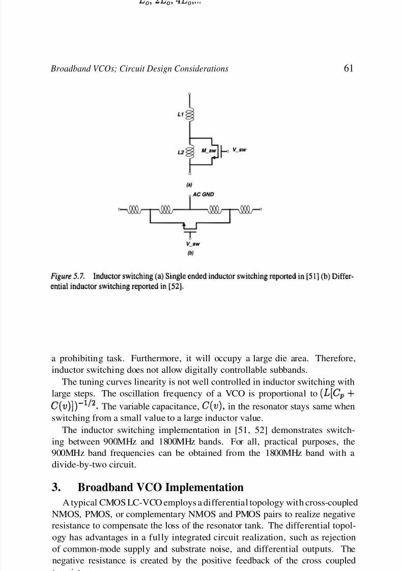
Inductance Switching
Switching inductors in the LC-tank are also feasible and shown in [51‚ 52]‚Single ended and differential switching is shown in Figure 5.7(a) and (b)‚ re-
spectively. Differential switching of inductor has the benefit of reduction of
series resistance and parasitic capacitance‚ by a factor of 2‚ to the RF nodes in
the tank.
Switching the inductors suffers from the CMOS switch loss as in the case
switching capacitance. The switch loss is more pronounced in the inductor case
since the quality factor of an on-chip inductor is already smaller than that of the
capacitance. If the switches are designed for minimum series resistance to avoid
deteriorating of the Q of the tank‚ then a large parasitic switch capacitance isintroduced at the RF-nodes of the tank which leads to high power consumption
and phase noise.
Implementation of equally spaced subbands as shown in Figure 4.5(b) is
difficult with switching the inductors. This requires an implementation of a
binary-weighted inductor switching structure which in turn implies implement-
ing several inductors‚ Characterization of such a structure is
8/6/2019 5.Broadband.vcos 1449
http://slidepdf.com/reader/full/5broadbandvcos-1449 11/25
Broadband VCOs; Circuit Design Considerations 61
a prohibiting task. Furthermore‚ it will occupy a large die area. Therefore‚
inductor switching does not allow digitally controllable subbands.
The tuning curves linearity is not well controlled in inductor switching with
large steps. The oscillation frequency of a VCO is proportional to
The variable capacitance‚ in the resonator stays same when
switching from a small value to a large inductor value.
The inductor switching implementation in [51‚ 52] demonstrates switch-
ing between 900MHz and 1800MHz bands. For all‚ practical purposes‚ the
900MHz band frequencies can be obtained from the 1800MHz band with a
divide-by-two circuit.
3. Broadband VCO Implementation
A typical CMOS LC-VCO employs a differential topology with cross-coupledNMOS‚ PMOS‚ or complementary NMOS and PMOS pairs to realize negative
resistance to compensate the loss of the resonator tank. The differential topol-
ogy has advantages in a fully integrated circuit realization‚ such as rejection
of common-mode supply and substrate noise‚ and differential outputs. The
negative resistance is created by the positive feedback of the cross coupled
transistors.

8/6/2019 5.Broadband.vcos 1449
http://slidepdf.com/reader/full/5broadbandvcos-1449 12/25
62 CMOS PLLs AND VCOs FOR 4G WIRELESS
Active Circuit Design
The versions of the differential topology with cross-coupled pair are shown
in Figure 5.8. The selection of a topology depends on specifications of the VCO
(phase noise‚ power consumption‚ and tuning range) and the process technology.
The NMOS only topology shown in Figure 5.8(a) has the advantage of higher
transconductance per area compared to PMOS only topology shown in Fig-
ure 5.8(b) due to higher mobility of electrons in NMOS devices‚ and hence
smaller transistor capacitances will contribute to the total parasitic capacitance
of the resonator tank. However‚ PMOS devices have lower flicker noise densi-ties than NMOS devices.
For the NMOS and PMOS complementary topology (Figure 5.8(c))‚ power
consumption is lower than that of the NMOS only or PMOS only topologies
because the bias current is reused. This topology is use-able where there is
enough supply voltage headroom for stacking the transistors. As the channel
length shrinks with sub-micron CMOS technology‚ the available supply voltage
does shrink but not of MOS devices. The nominal supply voltages for 0.1 Sum
and 0.1 Sum CMOS technologies are 1.8V and 1.25V‚ respectively. The nominal
threshold voltages for these technologies are 0.5V and 0.4V‚ respectively.
The topologies shown in Figure 5.8 use current biasing for active devices.
The current biasing serves two purposes; (i) limiting the output amplitude of
VCO‚ and hence preventing devices from going into deep triode region which
degrades phase noise performance [53] (ii) presents high impedance to the node
connected to the resonator to decouple supply or ground from the resonator. The
bias current can be suplied from the supply or ground sides. If there is available
headroom‚ bias current can be enforced from both sides. Usually‚ the supplyside is preferred to reduce the supply sensitivity of the output frequency of the
VCO. Unfortunately‚ the bias current noise is one of the major contributors to
the phase noise of the VCO. The VCO acts as mixer for bias noise and translates
low frequency bias noise into sidebands around oscillation frequency.
The small signal admittance seen at the the drain of M1 and M2 transistors
in Figure 5.8(a) and (b) pairs is equal to where is the small-
signal transconductance of each transistor. The MOS transconductance‚ is
written in the saturation region as;
where is a fixed process dependent design parameter. The transistor
geometry‚ and the DC bias point‚ are chosen to achieve a
desired

8/6/2019 5.Broadband.vcos 1449
http://slidepdf.com/reader/full/5broadbandvcos-1449 13/25
Broadband VCOs: Circuit Design Considerations 63

8/6/2019 5.Broadband.vcos 1449
http://slidepdf.com/reader/full/5broadbandvcos-1449 14/25
64 CMOS PLLs AND VCOs FOR 4G WIRELESS
A trade-off exists between power savings‚ tuning range‚ and phase noise
performance when choosing transistor size‚ and bias pointTo lower power consumption‚ has to be as low as possible. In
that case‚ must be increased to obtain a desired value. This will lead
to large parasitic capacitances adding to the capacitance of the resonant tank
which results in reducing the available tuning range.
Furthermore‚ minimizing and value to reduce power con-
sumption and increase tuning range will yield a small oscillation amplitude
The smaller oscillation amplitude results in poor phase noise
performance since phase noise is inversely proportional to the square of oscil-
lation amplitude‚ i.e.‚
Minimizing the power consumption in aVCO requires sacrifices from tuning
range and phase noise peformance. Maximizing tuning range yields higher
power consumption and phase noise. Minimum phase noise requires narrow
tuning range (larger L / C ratio) and highest output amplitude (power consump-
tion).
The negative resistance seen at the active circuit port (Figure 5.8)‚
must be chosen at least two times greater than the resonant tank effective
resistance to guarantee the start up of oscillation [11‚ 13].
Programmable Bias Current
A VCO bias current can be made programmable in order to dynamically
change the VCO core current for VCO amplitude adjustment when the resonator
Q is low due to process variation‚ temperature‚ or supply voltage variation. Also‚
the resonator Q varies over the tuning range for broadband VCOs. In steady-
state operation‚ oscillator active devices operate as switches rather than a small
signal negative resistance. The current fed to the resonator tank is limited bythe current mirrors in the oscillator bias circuit and becomes a square wave with
a peak current The output amplitude of the oscillator can be approximated
by using the first Fourier component in the current [54];
where is the current fed to the resonator by active devices and is the
peak voltage over the resonator equivalent tank resistance‚ at the steady-state which equals to the peak to peak value of one single-ended output. From
Equation 5.22‚ the oscillator output amplitude is primarily dependent on the
resonator equivalent resistance and the active device bias current. A simple
method to keep the VCO amplitude constant or at the desired level over the
frequency band of interest is to keep the product of constant. This
can be done or implemented several ways. Automatic-amplitude control (AAC)

8/6/2019 5.Broadband.vcos 1449
http://slidepdf.com/reader/full/5broadbandvcos-1449 15/25
Broadband VCOs: Circuit Design Considerations 65
circuit can be implemented [54‚ 55]. An extensive discussions of digital and
analog AAC for VCOs can be found in Reference [54].Amplitude control circuit is needed in broadband VCOs to guarantee a proper
operation over a wide tuning range. Two different architectures to correct the
amplitude of the broadband VCO are shown in Figure 5.9. Figure 5.9(a) shows
digital amplitude correction circuit with an ADC circuit. Figure 5.9(b) shows
digital current control depending on sub-band selection code in a band switching
tuning scheme. An implementation of the programmable bias block is also
shown in Figure 5.9(c). The TR(0:N) is the sub-band selection code in a band
switching tuning scheme.
Bias Noise Filtering
Bias filtering is necessary to suppress the noise from band-gap reference
current noise‚ noise coupled reference current line and noise from the digital
control inputs in the bias circuit shown in Figure 5.9. A typical low-pass bias
filter is shown in Figure 5.10(a). The product determines the noise
bandwidth. The noise bandwidth of the low pass filter should be less than the
PLL loop bandwidth since the PLL suppresses the VCO noise inside the PLL
loop bandwidth.
Typical resistors (high-resistivity poly) and capacitors (MIM and poly-poly)
in CMOS technology consume large die area. A solution is proposed for this as
shown in Figure 5.10(b). The resistor is implemented by using a MOS device
in ohmic region while a MOS device is used as capacitor. Implementing a large
resistor with MOS device takes less die area than MOS capacitor. Hence‚ it is
desirable to make the resistance large and the capacitance small while keeping
the RC product constant. The MOS device resistance in the triode region is
given by;
The resistance of the MOS device is function of and The
bias voltage‚ sets the resistance of the MOS device in Figure 5.10(b).
Another consideration for bias filter design is the time constant of the filter
which determines the start-up time of the VCO. If the bias filter cut-off frequency
is then the start-up time will be around
This severely affects the PLL lock time. To speed-up the start-up of the VCO‚proposed solutions are shown in Figure 5.11. A delay in power down circuit
in the bias filter of Figure 5.11 (a) is added to speed-up the start-up. The MOS
device‚ is used as a switch to bypass the bias filter resistor at start-up.
A delay in the bias filter of Figure 5.11(b) is implemented dynamically. The
MOS device‚ exhibits small resistance at power-up since the node X in
Figure 5.11(b) is at voltage level. Once and start conducting
8/6/2019 5.Broadband.vcos 1449
http://slidepdf.com/reader/full/5broadbandvcos-1449 16/25
66 CMOS PLLs AND VCOs FOR 4G WIRELESS
current‚ the voltage at node X decreases from to and hence the
resistance of increases.

8/6/2019 5.Broadband.vcos 1449
http://slidepdf.com/reader/full/5broadbandvcos-1449 17/25
Broadband VCOs: Circuit Design Considerations 67
4. Resonator Tank Design
The key parameter for a fully integrated VCO performance is the quality
factor of on-chip inductors‚ capacitors‚and varactors. The loaded Q of the
resonator tank is primarily determined by the quality factor of on-chip inductors
and varactors. This section overviews integrated inductors and varactors.
Integrated Inductors
Inductors can be implemented in three different ways in IC technology; (i)external off-chip inductors (ii) packaging bond-wires as inductors (iii) on-chip
spiral inductors.
The use of external resonators (inductors or striplines) is not preferred with
CMOS technology for several reasons. The pin parasitics of the package will
limit the usable values. The crosstalk paths between pins will inject noise into
the resonator tank and degrade the noise performance of the VCO. Also‚ BSD

8/6/2019 5.Broadband.vcos 1449
http://slidepdf.com/reader/full/5broadbandvcos-1449 18/25
68 CMOS PLLs AND VCOs FOR 4G WIRELESS
(electro-static discharge) protection networks in CMOS are probably the major
factor preventing the implementation of external resonator tanks.Although bondwire inductors have a very high quality factor‚ they are not
commonly used in VCOs because of lack of reproducibility and mechanical sta-
bility. An excellent review of design and implementation of bondwire inductors
can be found in the reference [9].
On-chip integrated inductors are favored over off-chip ones because pad
and bond wire parasitics are eliminated. Also‚ on-chip inductors exhibit good
reproducibility since the inductor value is mainly determined by horizontal
dimensions which are tightly controlled by lithographic resolution in any CMOS
technology. The major drawback of on-chip inductors is the low-Q factor
and large die area. On-chip integrated inductors are bu il t in spiral geometries
including squares‚ octagons and circles as shown in Figure 5.12. Compared to a
circular inductor‚ a square spiral inductor has larger inductance-to-area ratio but
contributes more series resistance which is due to longer overall metal length
for a given inductance value. Therefore‚ a spiral structure that more closely
approximates a circle (whenever technology permits) is preferred to increase
the quality factor.
The most important parameter for an integrated inductor is the quali ty factor.
The quality factor of integrated inductors in CMOS technology suffers from
three loss mechanisms; metal sheet resistance (ohmic loss)‚ capacitive coupling
to the substrate‚ and magnetic coupling to the substrate [7]. Approaches to
reduce these losses and obtain high Q on-chip inductors are listed below;
Reduce metal sheet resistance by using thicker metalization [56]‚ stacking
of metal layers‚ and using lower resistivity metals (e.g. copper) [57].
Make the dielectric layer between metal layers and the substrate as thick as
possible by using top metal layers.

8/6/2019 5.Broadband.vcos 1449
http://slidepdf.com/reader/full/5broadbandvcos-1449 19/25
Broadband VCOs: Circuit Design Considerations 69
Reduce substrate losses by using high-resistivity substrate [58]‚
by selectively removing the underlying substrate with post-fabrication steps [59]‚by using patterned ground shield (This method is quite useful for low-
resistivity substrates‚ [60].
All approaches depend on the technology parameters. Modern RF CMOS
technologies offer a thick top metal layer between on a medium resis-
tivity substrate
One of the key issues in the use of an on-chip inductor in a circuit design
is the adequate prediction of its behavior. A straightforward method used by
CMOS foundries is to fabricate and measure a whole batch of inductors with
varying geometries. A library of inductors is obtained from measurement data.
This library is also extended by fitting measurement data to simple models.
The fitted simple models allow only changes in one of the geometry parameters
around measured inductors‚ and hence limiting the available inductors to a
certain subset of the measured inductors. This is obviously not well suited for
optimum VCO inductor design since the maximum Q and the smallest die are
needed at a given frequency of interest.
Another approach is to use an electromagnetic (EM) simulator to character-ize the behavior of a specific inductor structure. Commercial and free softwares
are available for on-chip inductor simulations such as Agilent Momentum [61]‚
FEMLAB [62]‚ Sonnet [63] and ASITIC [64]. Every simulator has its own
strengths and disadvantages such as speed‚ accuracy‚ user interface‚ technical
support‚ etc. It is beneficial to have some familiarity with the methods used in
the simulators. ASITIC (Analysis of Si Inductors and transformers for ICs) is
used for inductor simulation in this book [64‚ 65]. ASITIC can simulate induc-
tance L‚ series resistance substrate capacitance and and substrate
resistance and and all the parameters are shown in Figure 5.13.
Simple formulas for estimating the inductor value for a given geometry can
be found in Reference [66]. The general relationship between an inductor and

8/6/2019 5.Broadband.vcos 1449
http://slidepdf.com/reader/full/5broadbandvcos-1449 20/25
70 CMOS PLLs AND VCOs FOR 4G WIRELESS
its geometrical dimensions can be expressed as follows;
where N is the number of turns‚ A is the cross-sectional area‚ and is the
total length of the spiral inductor. By connecting two layers of spiral inductors
in series‚ inductance can be increased by 4 times with the same inductor area
since inductance value is proportional to Moreover‚ the series resistance is
proportional to N resulting in the quality factor of the inductor being improved
simultaneously. However‚ the quality-factor of two-layer inductors is smaller
than twice that of single-layer inductors since the lower layer of metal usually
has a higher sheet resistance and larger substrate capacitances.To increase the
inductance while maintaining reasonable quality factor‚ multi-layer inductors
can be used [67].
Differential Inductor
Spiral inductors also can be implemented in differential structure as shown
in Figure 5.14. Differential inductors exhibit higher Q‚ better common mode
rejection‚ and smaller die area due to smaller parasitic capacitance (about half)than two single-ended inductors [68]. A differential inductor can be viewed as
two single-ended inductors inter-wounded symmetrically. A single differential
spiral inductor shown in Figure 5.15(a) can be used to replace a pair of single
ended inductors in the physical layout Figure 5.15(b).
Simulated model parameters for the inductors shown in Figure 5.15 are‚
Two single ended inductors;
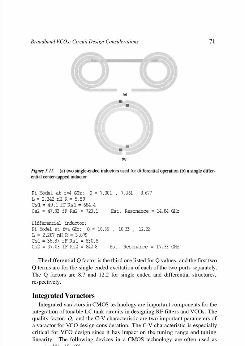
8/6/2019 5.Broadband.vcos 1449
http://slidepdf.com/reader/full/5broadbandvcos-1449 21/25
Broadband VCOs: Circuit Design Considerations 71
Pi Model at f=4 GHz: Q = 7.301 ‚ 7.361 ‚ 8.677
L = 2.342 nH R = 5.59
Cs1 = 49.1 fF Rs1 = 684.4
Cs2 = 47.82 fF Rs2 = 723.1 Est. Resonance = 14.84 GHz
Differential inductor:
Pi Model at f=4 GHz: Q = 10.35 ‚ 10.33 ‚ 12.22
L = 2.287 nH R = 3.879
Cs1 = 36.87 fF Rs1 = 830.8Cs2 = 37.03 fF Rs2 = 842.8 Est. Resonance = 17.33 GHz
The differential Q factor is the third one listed for Q values‚ and the first two
Q terms are for the single ended excitation of each of the two ports separately.
The Q factors are 8.7 and 12.2 for single ended and differential structures‚
respectively.
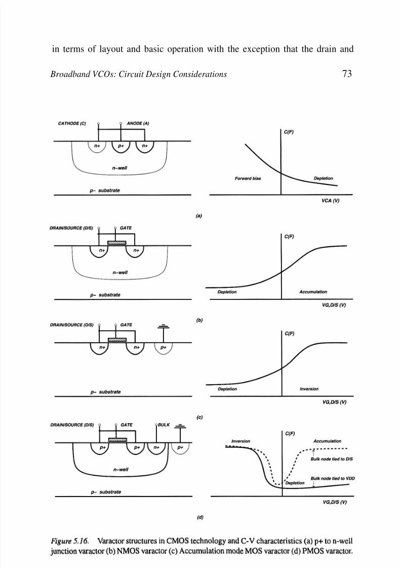
Integrated Varactors
Integrated varactors in CMOS technology are important components for theintegration of tunable LC tank circuits in designing RF filters and VCOs. The
quality factor‚ Q‚ and the C-V characteristic are two important parameters of
a varactor for VCO design consideration. The C-V characteristic is especially
critical for VCO design since it has impact on the tuning range and tuning
linearity. The following devices in a CMOS technology are often used as
varactor [44‚ 45‚ 69];

8/6/2019 5.Broadband.vcos 1449
http://slidepdf.com/reader/full/5broadbandvcos-1449 22/25
72 CMOS PLLs AND VCOs FOR 4G WIRELESS
(i) p+ to n-well junction
(ii) Accumulation Mode MOS (AMOS)
(iii) Standard Mode NMOS
(iv) Standard Mode PMOS
The first three devices are often preferred in VCO design because they use
electrons as majority carriers. As the mobility of electrons is higher than the
mobility of holes‚ the n-type varactors are expected to show higher Q than
p-type ones [45].
p+ to n-well junction
The p+ to n-well junction varactor utilizes the junction capacitance as-
sociated with the depletion region between the and the n-well as
shown in Figure 5.16(a). The value of thejunction capacitance is controlled
by the reverse voltage, which is defined from the Cathode (C) to the Anode (A).
The varactor capacitance, can be expressed as,
where is zero-bias junction capacitance‚ is the reverse DC voltage
across the junction in Figure5.16(a))‚ is the junction potential‚ and M
is the grading coefficient.
Accumulation Mode MOS
The Accumulation Mode NMOS varactor is a n-channel MOS placed inan n-well as shown in Figure 5.16(b). The varactor function is achieved by
changing the mode of operation from depletion to accumulation, by which the
capacitance is changed from minimum to maximum. With a negative voltage
applied between the gate and the drain/source, electrons just beneath the gate are
pushed away and a depleted area is created, in which the total capacitance from
gate to drain/source, is the series connection of the oxide capacitance,and the depletion capacitance, If the voltage is reversed so that a
positive voltage is applied between the gate and the drain/source, the silicon
surface is accumulated with electrons from the two -diffusion areas,is then obtaining its maximum value, which is equal to the oxide capacitance
Standard Mode NMOS
The Standard Mode NMOS varactor is the same as the n-channel MOS
in terms of layout and basic operation with the exception that the drain and
8/6/2019 5.Broadband.vcos 1449
http://slidepdf.com/reader/full/5broadbandvcos-1449 23/25
Broadband VCOs: Circuit Design Considerations 73

8/6/2019 5.Broadband.vcos 1449
http://slidepdf.com/reader/full/5broadbandvcos-1449 24/25
74 CMOS PLLs AND VCOs FOR 4G WIRELESS
source are shorted to form a single terminal as shown in Figure 5.16(c). The
varactor function is achieved by changing the mode of operation from depletionto inversion‚ by which the capacitance is changed from minimum to maximum.
With a small positive voltage applied between the gate (G) and the drain/source
(D/S) a depletion region is created just beneath the gate. In this situation the total
capacitance from gate to drain/source‚ equals the series connection of
the oxide capacitance and the depletion capacitance If the gate voltage
is increased‚ the depletion region beneath the gate will extend deeper into the
substrate‚ which will cause and consequently to increase. When the
gate voltage is increased even further‚ an inversion layer (channel) is created at
the silicon surface. When strong inversion is reached‚ the will obtain
its maximum value‚ which is equal to the oxide capacitance
Standard Mode PMOS
The Standard Mode PMOS varactor is the same as the p-channel MOS in
terms of layout and basic operation with the exception that the drain and source
are shorted to form a single terminal as shown in Figure 5.16(d). It has third
terminal because of the n-well connection‚ ’Bulk’. It can exhibit different C-V
characteristics depending on the bulk terminal biasing. The C-V characteris-tics are shown in Figure 5.16(d) when the bulk is tied to drain/source (D/S)
terminal or VDD. The varactor function is achieved by changing the mode of
operation from inversion to depletion when the bulk is tied to VDD by which
the capacitance is changed from maximum to minimum. When the bulk is tied
to the D/S terminal‚ the mode of operation exercises inversion‚ depletion‚ and
accumulation as well. With strong inversion and accumulation‚ the
will obtain its maximum value‚ which is equal to the oxide capacitance
The actual voltage applied across to the varactor device terminals is composed
of DC voltage and large signal AC voltage. Therefore‚ the C-V curve calculated
for DC voltage differs from the large signal added. The C-V curve under
large signal condition depends on the amplitude of the signal applied across its
terminals along with DC voltage. The effective capacitance is obtained through
averaging the instantaneous capacitance over one oscillation period for VCO
operation. A test structure to simulate the C-V characteristic of a PMOS device
is shown in Figure 5.17(a) with a DC voltage applied across the terminals
and along with sine wave with amplitude The simulated C-V curve is
shown in Figure 5.17(b).
5. Summary
In this chapter‚ the design and implementation of broadband VCOs at the
circuit level are described. Broadband tuning is implemented with discrete
and continuous tuning control mechanisms to reduce VCO tuning sensitivity‚
and hence reduce phase noise due to tuning control line. The discrete tuning is

8/6/2019 5.Broadband.vcos 1449
http://slidepdf.com/reader/full/5broadbandvcos-1449 25/25
Broadband VCOs: Circuit Design Considerations 75
implemented with capacitance switching. Differential structures are favored for
lower switch resistance and better common mode noise rejection. Active circuit
design techniques are also discussed. The selection of a certain active circuittopology depends on the design requirements. The use of PMOS devices may
lead to lower flicker noise. Integrated inductors and varactors are also described.