5100 ES Series Portable Radio Service Manual -...
180
5100 ES Series Portable Radio Service Manual UHF / 700 / 800 MHz Project 25 Conventional and Trunked Analog and Digital Conventional SMARTNET ® /SmartZone ® 7.2 VDC 4 Watt (UHF), 2.5 Watt (700 MHz), 3 Watt (800 MHz) Part Number 001-5100-60001 January 2007
-
Upload
truongkien -
Category
Documents
-
view
228 -
download
1
Transcript of 5100 ES Series Portable Radio Service Manual -...

5100 ES Series Portable RadioService Manual
UHF / 700 / 800 MHz
Project 25 Conventional and TrunkedAnalog and Digital Conventional
SMARTNET®/SmartZone®
7.2 VDC4 Watt (UHF), 2.5 Watt (700 MHz), 3 Watt (800 MHz)
Part Number 001-5100-60001January 2007


Copyright © 2007 by the E.F. Johnson Company
The EFJohnson logo, PC Configure™, Trunked IP25™, and Call Guard® are trademarks of EFJohnson. All other company and/or product names used in this manual are trademarks and/or registered trademarks of
their respective manufacturers.
Information in this manual is subject to change without notice.
5100 ES Series Portable Radio Service Manual
January 2007


January 2007 5100 ES Series Portable Radio Service Manual i
Table of Contents1 General Information 1-1
Scope of Manual . . . . . . . . . . . . . . . . . . . . . . . . . . . . . . . . . . . . . . . . . . . . . . . . . . . . . . . . . . . . . . . . 1-1
Radio Description. . . . . . . . . . . . . . . . . . . . . . . . . . . . . . . . . . . . . . . . . . . . . . . . . . . . . . . . . . . . . . . 1-2General . . . . . . . . . . . . . . . . . . . . . . . . . . . . . . . . . . . . . . . . . . . . . . . . . . . . . . . . . . . . . . . . . . . 1-2Analog/Digital Operation . . . . . . . . . . . . . . . . . . . . . . . . . . . . . . . . . . . . . . . . . . . . . . . . . . . . . . 1-3Operating Protocols . . . . . . . . . . . . . . . . . . . . . . . . . . . . . . . . . . . . . . . . . . . . . . . . . . . . . . . . . 1-3Systems, Channels, and Zones . . . . . . . . . . . . . . . . . . . . . . . . . . . . . . . . . . . . . . . . . . . . . . . . 1-3
Systems. . . . . . . . . . . . . . . . . . . . . . . . . . . . . . . . . . . . . . . . . . . . . . . . . . . . . . . . . . . . . . 1-3Channels . . . . . . . . . . . . . . . . . . . . . . . . . . . . . . . . . . . . . . . . . . . . . . . . . . . . . . . . . . . . . 1-4Zones. . . . . . . . . . . . . . . . . . . . . . . . . . . . . . . . . . . . . . . . . . . . . . . . . . . . . . . . . . . . . . . . 1-4
Programming. . . . . . . . . . . . . . . . . . . . . . . . . . . . . . . . . . . . . . . . . . . . . . . . . . . . . . . . . . . . . . . 1-4Alignment . . . . . . . . . . . . . . . . . . . . . . . . . . . . . . . . . . . . . . . . . . . . . . . . . . . . . . . . . . . . . . . . . 1-4
Part Number Breakdown . . . . . . . . . . . . . . . . . . . . . . . . . . . . . . . . . . . . . . . . . . . . . . . . . . . . . . . . . 1-5
Transceiver Identification . . . . . . . . . . . . . . . . . . . . . . . . . . . . . . . . . . . . . . . . . . . . . . . . . . . . . . . . 1-6
Accessories . . . . . . . . . . . . . . . . . . . . . . . . . . . . . . . . . . . . . . . . . . . . . . . . . . . . . . . . . . . . . . . . . . . 1-6
Intrinsically Safe Information . . . . . . . . . . . . . . . . . . . . . . . . . . . . . . . . . . . . . . . . . . . . . . . . . . . . . 1-9Introduction . . . . . . . . . . . . . . . . . . . . . . . . . . . . . . . . . . . . . . . . . . . . . . . . . . . . . . . . . . . . . . . . 1-9Definitions . . . . . . . . . . . . . . . . . . . . . . . . . . . . . . . . . . . . . . . . . . . . . . . . . . . . . . . . . . . . . . . . 1-10Possible Ignition Sources . . . . . . . . . . . . . . . . . . . . . . . . . . . . . . . . . . . . . . . . . . . . . . . . . . . . 1-10Intrinsically Safe and Nonincendive Ratings . . . . . . . . . . . . . . . . . . . . . . . . . . . . . . . . . . . . . . 1-11Classification of Hazardous Areas and Atmospheres . . . . . . . . . . . . . . . . . . . . . . . . . . . . . . . 1-11
Classification of Hazardous Areas (Division). . . . . . . . . . . . . . . . . . . . . . . . . . . . . . . . . 1-12Atmosphere Classification (Class/Group) . . . . . . . . . . . . . . . . . . . . . . . . . . . . . . . . . . . 1-12
Secure Communication . . . . . . . . . . . . . . . . . . . . . . . . . . . . . . . . . . . . . . . . . . . . . . . . . . . . . . . . . 1-13
Typical Performance Specifications . . . . . . . . . . . . . . . . . . . . . . . . . . . . . . . . . . . . . . . . . . . . . . . 1-14
2 Battery, Accessory and Disassembly Information 2-1Battery Information . . . . . . . . . . . . . . . . . . . . . . . . . . . . . . . . . . . . . . . . . . . . . . . . . . . . . . . . . . . . . 2-1
Battery Removal/Installation . . . . . . . . . . . . . . . . . . . . . . . . . . . . . . . . . . . . . . . . . . . . . . . . . . . 2-1Battery Charging . . . . . . . . . . . . . . . . . . . . . . . . . . . . . . . . . . . . . . . . . . . . . . . . . . . . . . . . . . . . 2-2Preventing Loss of Encryption Keys . . . . . . . . . . . . . . . . . . . . . . . . . . . . . . . . . . . . . . . . . . . . . 2-2Battery Care . . . . . . . . . . . . . . . . . . . . . . . . . . . . . . . . . . . . . . . . . . . . . . . . . . . . . . . . . . . . . . . 2-2
Belt Clip Installation . . . . . . . . . . . . . . . . . . . . . . . . . . . . . . . . . . . . . . . . . . . . . . . . . . . . . . . . . . . . . 2-3
5100 ES Series Portable RadioService Manual
January 2007
ii 5100 ES Series Portable Radio Service Manual January 2007
Table of Contents (continued)
Accessory Installation . . . . . . . . . . . . . . . . . . . . . . . . . . . . . . . . . . . . . . . . . . . . . . . . . . . . . . . . . . . 2-3Option Select Lines . . . . . . . . . . . . . . . . . . . . . . . . . . . . . . . . . . . . . . . . . . . . . . . . . . . . . . . . . . 2-4
Transceiver Disassembly. . . . . . . . . . . . . . . . . . . . . . . . . . . . . . . . . . . . . . . . . . . . . . . . . . . . . . . . . 2-5Separating Front Cover and Chassis . . . . . . . . . . . . . . . . . . . . . . . . . . . . . . . . . . . . . . . . . . . . 2-5Removing RF and Logic Boards From Chassis . . . . . . . . . . . . . . . . . . . . . . . . . . . . . . . . . . . . 2-6Removing UI (User Interface) Board. . . . . . . . . . . . . . . . . . . . . . . . . . . . . . . . . . . . . . . . . . . . . 2-7Removing Switch Assembly . . . . . . . . . . . . . . . . . . . . . . . . . . . . . . . . . . . . . . . . . . . . . . . . . . . 2-7
3 Operation 3-1General . . . . . . . . . . . . . . . . . . . . . . . . . . . . . . . . . . . . . . . . . . . . . . . . . . . . . . . . . . . . . . . . . . . . . . . 3-1
4 Transceiver Programming 4-1Programming Setup . . . . . . . . . . . . . . . . . . . . . . . . . . . . . . . . . . . . . . . . . . . . . . . . . . . . . . . . . . . . . 4-1
Computer Description . . . . . . . . . . . . . . . . . . . . . . . . . . . . . . . . . . . . . . . . . . . . . . . . . . . . . . . . . . . 4-2
Using the PC Configure Software . . . . . . . . . . . . . . . . . . . . . . . . . . . . . . . . . . . . . . . . . . . . . . . . . . 4-2
Firmware Upgrade Instructions . . . . . . . . . . . . . . . . . . . . . . . . . . . . . . . . . . . . . . . . . . . . . . . . . . . 4-2Upgrade Utility Compatibility . . . . . . . . . . . . . . . . . . . . . . . . . . . . . . . . . . . . . . . . . . . . . . . . . . . 4-2Firmware Upgrade instructions . . . . . . . . . . . . . . . . . . . . . . . . . . . . . . . . . . . . . . . . . . . . . . . . . 4-3
Requirements . . . . . . . . . . . . . . . . . . . . . . . . . . . . . . . . . . . . . . . . . . . . . . . . . . . . . . . . . 4-3PC Configure Upgrade Instructions. . . . . . . . . . . . . . . . . . . . . . . . . . . . . . . . . . . . . . . . . 4-4Initial Setup . . . . . . . . . . . . . . . . . . . . . . . . . . . . . . . . . . . . . . . . . . . . . . . . . . . . . . . . . . . 4-4Firmware Upgrade Procedure . . . . . . . . . . . . . . . . . . . . . . . . . . . . . . . . . . . . . . . . . . . . . 4-5
Cloning Procedure . . . . . . . . . . . . . . . . . . . . . . . . . . . . . . . . . . . . . . . . . . . . . . . . . . . . . . . . . . . . . . 4-6
5 Circuit Description 5-1General Overview . . . . . . . . . . . . . . . . . . . . . . . . . . . . . . . . . . . . . . . . . . . . . . . . . . . . . . . . . . . . . . . 5-1
Introduction . . . . . . . . . . . . . . . . . . . . . . . . . . . . . . . . . . . . . . . . . . . . . . . . . . . . . . . . . . . . . . . . 5-1PC Boards . . . . . . . . . . . . . . . . . . . . . . . . . . . . . . . . . . . . . . . . . . . . . . . . . . . . . . . . . . . . 5-1
Analog Mode . . . . . . . . . . . . . . . . . . . . . . . . . . . . . . . . . . . . . . . . . . . . . . . . . . . . . . . . . . . . . . . 5-2Receive Mode . . . . . . . . . . . . . . . . . . . . . . . . . . . . . . . . . . . . . . . . . . . . . . . . . . . . . . . . . 5-2Transmit Mode. . . . . . . . . . . . . . . . . . . . . . . . . . . . . . . . . . . . . . . . . . . . . . . . . . . . . . . . . 5-2
Project 25 Digital Mode . . . . . . . . . . . . . . . . . . . . . . . . . . . . . . . . . . . . . . . . . . . . . . . . . . . . . . . 5-3Receive Mode . . . . . . . . . . . . . . . . . . . . . . . . . . . . . . . . . . . . . . . . . . . . . . . . . . . . . . . . . 5-3Transmit Mode. . . . . . . . . . . . . . . . . . . . . . . . . . . . . . . . . . . . . . . . . . . . . . . . . . . . . . . . . 5-3
UHF Low RF Board. . . . . . . . . . . . . . . . . . . . . . . . . . . . . . . . . . . . . . . . . . . . . . . . . . . . . . . . . . . . . . 5-3Receiver . . . . . . . . . . . . . . . . . . . . . . . . . . . . . . . . . . . . . . . . . . . . . . . . . . . . . . . . . . . . . . . . . . 5-5
Front End Bandpass Filter . . . . . . . . . . . . . . . . . . . . . . . . . . . . . . . . . . . . . . . . . . . . . . . . 5-5Front End LNA and Bypass Switching. . . . . . . . . . . . . . . . . . . . . . . . . . . . . . . . . . . . . . . 5-5Post-LNA Bandpass Filters . . . . . . . . . . . . . . . . . . . . . . . . . . . . . . . . . . . . . . . . . . . . . . . 5-5Mixer and LO Filter . . . . . . . . . . . . . . . . . . . . . . . . . . . . . . . . . . . . . . . . . . . . . . . . . . . . . 5-5IF Filter and Amplifier . . . . . . . . . . . . . . . . . . . . . . . . . . . . . . . . . . . . . . . . . . . . . . . . . . . 5-5Back End IC. . . . . . . . . . . . . . . . . . . . . . . . . . . . . . . . . . . . . . . . . . . . . . . . . . . . . . . . . . . 5-6

January 2007 5100 ES Series Portable Radio Service Manual iii
Table of Contents (continued)
Synthesizer . . . . . . . . . . . . . . . . . . . . . . . . . . . . . . . . . . . . . . . . . . . . . . . . . . . . . . . . . . . . . . . . 5-6PLL IC . . . . . . . . . . . . . . . . . . . . . . . . . . . . . . . . . . . . . . . . . . . . . . . . . . . . . . . . . . . . . . . 5-6Reference Oscillator . . . . . . . . . . . . . . . . . . . . . . . . . . . . . . . . . . . . . . . . . . . . . . . . . . . . 5-7Analog Switches and PLL Loop Filters . . . . . . . . . . . . . . . . . . . . . . . . . . . . . . . . . . . . . . 5-7VCOs . . . . . . . . . . . . . . . . . . . . . . . . . . . . . . . . . . . . . . . . . . . . . . . . . . . . . . . . . . . . . . . . 5-7
Transmitter . . . . . . . . . . . . . . . . . . . . . . . . . . . . . . . . . . . . . . . . . . . . . . . . . . . . . . . . . . . . . . . . 5-7Modulation . . . . . . . . . . . . . . . . . . . . . . . . . . . . . . . . . . . . . . . . . . . . . . . . . . . . . . . . . . . . 5-7Power Amplifier . . . . . . . . . . . . . . . . . . . . . . . . . . . . . . . . . . . . . . . . . . . . . . . . . . . . . . . . 5-7ALC . . . . . . . . . . . . . . . . . . . . . . . . . . . . . . . . . . . . . . . . . . . . . . . . . . . . . . . . . . . . . . . . . 5-8T/R Switching and Harmonic Filter . . . . . . . . . . . . . . . . . . . . . . . . . . . . . . . . . . . . . . . . . 5-8
700/800 MHz RF Board . . . . . . . . . . . . . . . . . . . . . . . . . . . . . . . . . . . . . . . . . . . . . . . . . . . . . . . . . . . 5-8Receiver . . . . . . . . . . . . . . . . . . . . . . . . . . . . . . . . . . . . . . . . . . . . . . . . . . . . . . . . . . . . . . . . . 5-10
Front End Bandpass Filter . . . . . . . . . . . . . . . . . . . . . . . . . . . . . . . . . . . . . . . . . . . . . . . 5-10Front End LNA and Bypass Switching. . . . . . . . . . . . . . . . . . . . . . . . . . . . . . . . . . . . . . 5-10Post-LNA Bandpass Filters . . . . . . . . . . . . . . . . . . . . . . . . . . . . . . . . . . . . . . . . . . . . . . 5-10Mixer and LO Filter . . . . . . . . . . . . . . . . . . . . . . . . . . . . . . . . . . . . . . . . . . . . . . . . . . . . 5-10IF Filter and Amplifier . . . . . . . . . . . . . . . . . . . . . . . . . . . . . . . . . . . . . . . . . . . . . . . . . . 5-11Back End IC. . . . . . . . . . . . . . . . . . . . . . . . . . . . . . . . . . . . . . . . . . . . . . . . . . . . . . . . . . 5-11
Synthesizer . . . . . . . . . . . . . . . . . . . . . . . . . . . . . . . . . . . . . . . . . . . . . . . . . . . . . . . . . . . . . . . 5-12PLL IC . . . . . . . . . . . . . . . . . . . . . . . . . . . . . . . . . . . . . . . . . . . . . . . . . . . . . . . . . . . . . . 5-12Reference Oscillator . . . . . . . . . . . . . . . . . . . . . . . . . . . . . . . . . . . . . . . . . . . . . . . . . . . 5-12Analog Switches and PLL Loop Filters . . . . . . . . . . . . . . . . . . . . . . . . . . . . . . . . . . . . . 5-12VCOs . . . . . . . . . . . . . . . . . . . . . . . . . . . . . . . . . . . . . . . . . . . . . . . . . . . . . . . . . . . . . . . 5-12
Transmitter . . . . . . . . . . . . . . . . . . . . . . . . . . . . . . . . . . . . . . . . . . . . . . . . . . . . . . . . . . . . . . . 5-13Modulation . . . . . . . . . . . . . . . . . . . . . . . . . . . . . . . . . . . . . . . . . . . . . . . . . . . . . . . . . . . 5-13Power Amplifier . . . . . . . . . . . . . . . . . . . . . . . . . . . . . . . . . . . . . . . . . . . . . . . . . . . . . . . 5-13ALC . . . . . . . . . . . . . . . . . . . . . . . . . . . . . . . . . . . . . . . . . . . . . . . . . . . . . . . . . . . . . . . . 5-13T/R Switching and Harmonic Filter . . . . . . . . . . . . . . . . . . . . . . . . . . . . . . . . . . . . . . . . 5-13
User Interface Board . . . . . . . . . . . . . . . . . . . . . . . . . . . . . . . . . . . . . . . . . . . . . . . . . . . . . . . . . . . 5-14Power Supplies . . . . . . . . . . . . . . . . . . . . . . . . . . . . . . . . . . . . . . . . . . . . . . . . . . . . . . . . . . . . 5-14MPC870 Processor . . . . . . . . . . . . . . . . . . . . . . . . . . . . . . . . . . . . . . . . . . . . . . . . . . . . . . . . . 5-15Flash Memory . . . . . . . . . . . . . . . . . . . . . . . . . . . . . . . . . . . . . . . . . . . . . . . . . . . . . . . . . . . . . 5-15SRAM . . . . . . . . . . . . . . . . . . . . . . . . . . . . . . . . . . . . . . . . . . . . . . . . . . . . . . . . . . . . . . . . . . . 5-15HPI Bus Multiplexer. . . . . . . . . . . . . . . . . . . . . . . . . . . . . . . . . . . . . . . . . . . . . . . . . . . . . . . . . 5-16Bus Configuration Logic . . . . . . . . . . . . . . . . . . . . . . . . . . . . . . . . . . . . . . . . . . . . . . . . . . . . . 5-16HC08 Microcontroller . . . . . . . . . . . . . . . . . . . . . . . . . . . . . . . . . . . . . . . . . . . . . . . . . . . . . . . 5-16SPI Flash. . . . . . . . . . . . . . . . . . . . . . . . . . . . . . . . . . . . . . . . . . . . . . . . . . . . . . . . . . . . . . . . . 5-16Audio Out . . . . . . . . . . . . . . . . . . . . . . . . . . . . . . . . . . . . . . . . . . . . . . . . . . . . . . . . . . . . . . . . 5-17Audio In . . . . . . . . . . . . . . . . . . . . . . . . . . . . . . . . . . . . . . . . . . . . . . . . . . . . . . . . . . . . . . . . . . 5-17
Logic Board. . . . . . . . . . . . . . . . . . . . . . . . . . . . . . . . . . . . . . . . . . . . . . . . . . . . . . . . . . . . . . . . . . . 5-19Power Supplies . . . . . . . . . . . . . . . . . . . . . . . . . . . . . . . . . . . . . . . . . . . . . . . . . . . . . . . . . . . . 5-19
Digital. . . . . . . . . . . . . . . . . . . . . . . . . . . . . . . . . . . . . . . . . . . . . . . . . . . . . . . . . . . . . . . 5-20Analog . . . . . . . . . . . . . . . . . . . . . . . . . . . . . . . . . . . . . . . . . . . . . . . . . . . . . . . . . . . . . . 5-20RF Deck. . . . . . . . . . . . . . . . . . . . . . . . . . . . . . . . . . . . . . . . . . . . . . . . . . . . . . . . . . . . . 5-20
DSP. . . . . . . . . . . . . . . . . . . . . . . . . . . . . . . . . . . . . . . . . . . . . . . . . . . . . . . . . . . . . . . . . . . . . 5-20Control Interface . . . . . . . . . . . . . . . . . . . . . . . . . . . . . . . . . . . . . . . . . . . . . . . . . . . . . . 5-21Transmit Operation . . . . . . . . . . . . . . . . . . . . . . . . . . . . . . . . . . . . . . . . . . . . . . . . . . . . 5-21Receive Operation. . . . . . . . . . . . . . . . . . . . . . . . . . . . . . . . . . . . . . . . . . . . . . . . . . . . . 5-21
HPI Bus Multiplexer. . . . . . . . . . . . . . . . . . . . . . . . . . . . . . . . . . . . . . . . . . . . . . . . . . . . . . . . . 5-22Codec . . . . . . . . . . . . . . . . . . . . . . . . . . . . . . . . . . . . . . . . . . . . . . . . . . . . . . . . . . . . . . . . . . . 5-22SEM Module . . . . . . . . . . . . . . . . . . . . . . . . . . . . . . . . . . . . . . . . . . . . . . . . . . . . . . . . . . . . . . 5-23

iv 5100 ES Series Portable Radio Service Manual January 2007
Table of Contents (continued)
6 Alignment Procedure 6-1PC Tune . . . . . . . . . . . . . . . . . . . . . . . . . . . . . . . . . . . . . . . . . . . . . . . . . . . . . . . . . . . . . . . . . . . . . . . 6-1
7 Troubleshooting 7-1Start Up Failure LED Indications. . . . . . . . . . . . . . . . . . . . . . . . . . . . . . . . . . . . . . . . . . . . . . . . . . . 7-1
User Troubleshooting . . . . . . . . . . . . . . . . . . . . . . . . . . . . . . . . . . . . . . . . . . . . . . . . . . . . . . . . . . . 7-2
Low Battery Indicators. . . . . . . . . . . . . . . . . . . . . . . . . . . . . . . . . . . . . . . . . . . . . . . . . . . . . . . . . . . 7-2Battery Replacement. . . . . . . . . . . . . . . . . . . . . . . . . . . . . . . . . . . . . . . . . . . . . . . . . . . . . . . . . 7-2
Additional Information . . . . . . . . . . . . . . . . . . . . . . . . . . . . . . . . . . . . . . . . . . . . . . . . . . . . . . . . . . . 7-3
Contact Information . . . . . . . . . . . . . . . . . . . . . . . . . . . . . . . . . . . . . . . . . . . . . . . . . . . . . . . . . . . . . 7-3
8 Service Information 8-1Product Warranty . . . . . . . . . . . . . . . . . . . . . . . . . . . . . . . . . . . . . . . . . . . . . . . . . . . . . . . . . . . . . . . 8-1
Factory Customer Service . . . . . . . . . . . . . . . . . . . . . . . . . . . . . . . . . . . . . . . . . . . . . . . . . . . . . . . . 8-2
Returns for Repairs . . . . . . . . . . . . . . . . . . . . . . . . . . . . . . . . . . . . . . . . . . . . . . . . . . . . . . . . . . . . . 8-2
Replacement Parts . . . . . . . . . . . . . . . . . . . . . . . . . . . . . . . . . . . . . . . . . . . . . . . . . . . . . . . . . . . . . . 8-3
Internet Home Page . . . . . . . . . . . . . . . . . . . . . . . . . . . . . . . . . . . . . . . . . . . . . . . . . . . . . . . . . . . . . 8-4
9 Parts List 9-1Parts . . . . . . . . . . . . . . . . . . . . . . . . . . . . . . . . . . . . . . . . . . . . . . . . . . . . . . . . . . . . . . . . . . . . . . . . . 9-1
Exploded Views . . . . . . . . . . . . . . . . . . . . . . . . . . . . . . . . . . . . . . . . . . . . . . . . . . . . . . . . . . . . . . . 9-44
10 Schematic Diagrams and Component Layouts 10-1

January 2007 5100 ES Series Portable Radio Service Manual v
List of FiguresFigure Page
1.1 5100 ES Portable Radio Model I/II/III . . . . . . . . . . . . . . . . . . . . . . . . . . . . . . . . . . . . . . . 1-12.1 Battery Removal . . . . . . . . . . . . . . . . . . . . . . . . . . . . . . . . . . . . . . . . . . . . . . . . . . . . . . 2-12.2 Belt Clip Installation . . . . . . . . . . . . . . . . . . . . . . . . . . . . . . . . . . . . . . . . . . . . . . . . . . . . 2-32.3 Accessory Installation . . . . . . . . . . . . . . . . . . . . . . . . . . . . . . . . . . . . . . . . . . . . . . . . . . . 2-44.1 Programming Setup . . . . . . . . . . . . . . . . . . . . . . . . . . . . . . . . . . . . . . . . . . . . . . . . . . . . 4-15.1 UHF RF Board Block Diagram . . . . . . . . . . . . . . . . . . . . . . . . . . . . . . . . . . . . . . . . . . . . 5-45.2 700/800 MHz RF Board Block Diagram . . . . . . . . . . . . . . . . . . . . . . . . . . . . . . . . . . . . . 5-95.3 User Interface Board Block Diagram . . . . . . . . . . . . . . . . . . . . . . . . . . . . . . . . . . . . . . 5-185.4 Logic Board Block Diagram . . . . . . . . . . . . . . . . . . . . . . . . . . . . . . . . . . . . . . . . . . . . . 5-246.1 Alignment Setup . . . . . . . . . . . . . . . . . . . . . . . . . . . . . . . . . . . . . . . . . . . . . . . . . . . . . . . 6-19.1 5100 ES Portable Radio Model III Assembly . . . . . . . . . . . . . . . . . . . . . . . . . . . . . . . . 9-449.2 5100 ES Portable Radio Model II Assembly . . . . . . . . . . . . . . . . . . . . . . . . . . . . . . . . . 9-459.3 5100 ES Portable Radio Model I Assembly . . . . . . . . . . . . . . . . . . . . . . . . . . . . . . . . . 9-469.4 Front Housing Assembly Model III . . . . . . . . . . . . . . . . . . . . . . . . . . . . . . . . . . . . . . . . 9-479.5 Front Housing Assembly Model II . . . . . . . . . . . . . . . . . . . . . . . . . . . . . . . . . . . . . . . . . 9-489.6 Front Housing Assembly Model I . . . . . . . . . . . . . . . . . . . . . . . . . . . . . . . . . . . . . . . . . 9-499.7 Rear Housing Assembly Model I/II/III . . . . . . . . . . . . . . . . . . . . . . . . . . . . . . . . . . . . . . 9-509.8 User Interface PCB Assembly Model III . . . . . . . . . . . . . . . . . . . . . . . . . . . . . . . . . . . . 9-519.9 User Interface PCB Assembly Model II . . . . . . . . . . . . . . . . . . . . . . . . . . . . . . . . . . . . 9-529.10 User Interface PCB Assembly Model I . . . . . . . . . . . . . . . . . . . . . . . . . . . . . . . . . . . . . 9-539.11 Front Cover Assembly Model II/III . . . . . . . . . . . . . . . . . . . . . . . . . . . . . . . . . . . . . . . . 9-549.12 Front Cover Assembly Model I . . . . . . . . . . . . . . . . . . . . . . . . . . . . . . . . . . . . . . . . . . . 9-559.13 Front Cover Assembly Detail . . . . . . . . . . . . . . . . . . . . . . . . . . . . . . . . . . . . . . . . . . . . 9-5610.1 Interconnect Schematic . . . . . . . . . . . . . . . . . . . . . . . . . . . . . . . . . . . . . . . . . . . . . . . . 10-210.2 UHF RF Board Schematic (Page 1 of 5) . . . . . . . . . . . . . . . . . . . . . . . . . . . . . . . . . . . 10-310.3 UHF RF Board Schematic (Page 2 of 5) . . . . . . . . . . . . . . . . . . . . . . . . . . . . . . . . . . . 10-410.4 UHF RF Board Schematic (Page 3 of 5) . . . . . . . . . . . . . . . . . . . . . . . . . . . . . . . . . . . 10-510.5 UHF RF Board Schematic (Page 4 of 5) . . . . . . . . . . . . . . . . . . . . . . . . . . . . . . . . . . . 10-610.6 UHF RF Board Schematic (Page 5 of 5) . . . . . . . . . . . . . . . . . . . . . . . . . . . . . . . . . . . 10-710.7 UHF RF Board Layout . . . . . . . . . . . . . . . . . . . . . . . . . . . . . . . . . . . . . . . . . . . . . . . . . 10-810.8 700/800 MHz RF Board Schematic (Page 1 of 5) . . . . . . . . . . . . . . . . . . . . . . . . . . . . 10-910.9 700/800 MHz RF Board Schematic (Page 2 of 5) . . . . . . . . . . . . . . . . . . . . . . . . . . . 10-1010.10 700/800 MHz RF Board Schematic (Page 3 of 5) . . . . . . . . . . . . . . . . . . . . . . . . . . . 10-1110.11 700/800 MHz RF Board Schematic (Page 4 of 5) . . . . . . . . . . . . . . . . . . . . . . . . . . . 10-1210.12 700/800 MHz RF Board Schematic (Page 5 of 5) . . . . . . . . . . . . . . . . . . . . . . . . . . . 10-1310.13 700/800 MHz RF Board Layout . . . . . . . . . . . . . . . . . . . . . . . . . . . . . . . . . . . . . . . . . 10-1410.14 023-5500-180/182/185 Logic Board Schematic (Page 1 of 7) . . . . . . . . . . . . . . . . . . 10-1510.15 023-5500-180/182/185 Logic Board Schematic (Page 2 of 7) . . . . . . . . . . . . . . . . . . 10-1610.16 023-5500-180/182/185 Logic Board Schematic (Page 3 of 7) . . . . . . . . . . . . . . . . . . 10-1710.17 023-5500-180/182/185 Logic Board Schematic (Page 4 of 7) . . . . . . . . . . . . . . . . . . 10-1810.18 023-5500-180/182/185 Logic Board Schematic (Page 5 of 7) . . . . . . . . . . . . . . . . . . 10-19

vi 5100 ES Series Portable Radio Service Manual January 2007
List of Figures (continued)
Figure Page
10.19 023-5500-180/182/185 Logic Board Schematic (Page 6 of 7) . . . . . . . . . . . . . . . . . . 10-2010.20 023-5500-180/182/185 Logic Board Schematic (Page 7 of 7) . . . . . . . . . . . . . . . . . . 10-2110.21 023-5500-180/182/185 Logic Board Assembly . . . . . . . . . . . . . . . . . . . . . . . . . . . . . 10-2210.22 023-5500-480/485 User Interface Board Schematic (Page 1 of 10) . . . . . . . . . . . . . . 10-2310.23 023-5500-480/485 User Interface Board Schematic (Page 2 of 10) . . . . . . . . . . . . . . 10-2410.24 023-5500-480/485 User Interface Board Schematic (Page 3 of 10) . . . . . . . . . . . . . . 10-2510.25 023-5500-480/485 User Interface Board Schematic (Page 4 of 10) . . . . . . . . . . . . . 10-2610.26 023-5500-480/485 User Interface Board Schematic (Page 5 of 10) . . . . . . . . . . . . . . 10-2710.27 023-5500-480/485 User Interface Board Schematic (Page 6 of 10) . . . . . . . . . . . . . . 10-2810.28 023-5500-480/485 User Interface Board Schematic (Page 7 of 10) . . . . . . . . . . . . . . 10-2910.29 023-5500-480/485 User Interface Board Schematic (Page 8 of 10) . . . . . . . . . . . . . 10-3010.30 023-5500-480/485 User Interface Board Schematic (Page 9 of 10) . . . . . . . . . . . . . 10-3110.31 023-5500-480/485 User Interface Board Schematic (Page 10 of 10) . . . . . . . . . . . . 10-3210.32 023-5500-480/485 User Interface Board Assembly . . . . . . . . . . . . . . . . . . . . . . . . . . 10-3310.33 023-5500-480-01/487 User Interface Board Schematic (Page 1 of 10) . . . . . . . . . . . 10-3410.34 023-5500-480-01/487 User Interface Board Schematic (Page 2 of 10) . . . . . . . . . . . 10-3510.35 023-5500-480-01/487 User Interface Board Schematic (Page 3 of 10) . . . . . . . . . . . 10-3610.36 023-5500-480-01/487 User Interface Board Schematic (Page 4 of 10) . . . . . . . . . . . 10-3710.37 023-5500-480-01/487 User Interface Board Schematic (Page 5 of 10) . . . . . . . . . . . 10-3810.38 023-5500-480-01/487 User Interface Board Schematic (Page 6 of 10) . . . . . . . . . . . 10-3910.39 023-5500-480-01/487 User Interface Board Schematic (Page 7 of 10) . . . . . . . . . . . 10-4010.40 023-5500-480-01/487 User Interface Board Schematic (Page 8 of 10) . . . . . . . . . . . 10-4110.41 023-5500-480-01/487 User Interface Board Schematic (Page 9 of 10) . . . . . . . . . . . 10-4210.42 023-5500-480-01/487 User Interface Board Schematic (Page 10 of 10) . . . . . . . . . . 10-4310.43 023-5500-480-01/487 User Interface Board Assembly . . . . . . . . . . . . . . . . . . . . . . . . 10-4410.44 Cable Schematics . . . . . . . . . . . . . . . . . . . . . . . . . . . . . . . . . . . . . . . . . . . . . . . . . . . . 10-45
January 2007 5100 ES Series Portable Radio Service Manual vii
List of TablesTable Page
1.1 Accessories . . . . . . . . . . . . . . . . . . . . . . . . . . . . . . . . . . . . . . . . . . . . . . . . . . . . . . . . . . . 1-61.2 Area Classification . . . . . . . . . . . . . . . . . . . . . . . . . . . . . . . . . . . . . . . . . . . . . . . . . . . . . 1-121.3 Material Classification . . . . . . . . . . . . . . . . . . . . . . . . . . . . . . . . . . . . . . . . . . . . . . . . . . 1-121.4 5100 ES Portable Radio General Specifications . . . . . . . . . . . . . . . . . . . . . . . . . . . . . . 1-141.5 5100 ES Portable Radio Transmitter Specifications . . . . . . . . . . . . . . . . . . . . . . . . . . . 1-151.6 5100 ES Portable Radio Receiver Specifications . . . . . . . . . . . . . . . . . . . . . . . . . . . . . 1-151.7 5100 ES Portable Radio Batteries Specifications . . . . . . . . . . . . . . . . . . . . . . . . . . . . . 1-165.1 Multiplexer Logic Operation . . . . . . . . . . . . . . . . . . . . . . . . . . . . . . . . . . . . . . . . . . . . . . 5-167.1 Start Up Failure LED Indications . . . . . . . . . . . . . . . . . . . . . . . . . . . . . . . . . . . . . . . . . . . 7-1

viii 5100 ES Series Portable Radio Service Manual January 2007
List of Tables (continued)
Table Page
January 2007 5100 ES Series Portable Radio Service Manual 1-1
S E C T I O N
Chapter 1General Information
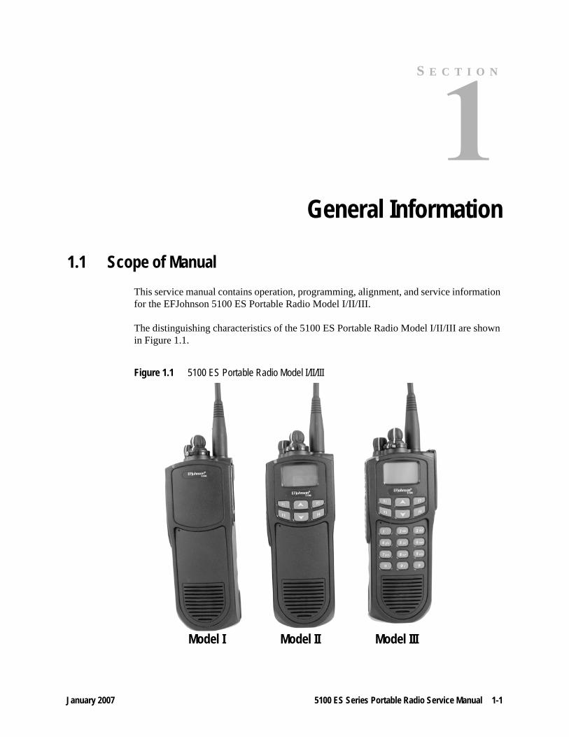
1.1 Scope of ManualThis service manual contains operation, programming, alignment, and service information for the EFJohnson 5100 ES Portable Radio Model I/II/III.
The distinguishing characteristics of the 5100 ES Portable Radio Model I/II/III are shown in Figure 1.1.
Figure 1.1 5100 ES Portable Radio Model I/II/III
Model IIModel I Model III

1-2 5100 ES Series Portable Radio Service Manual January 2007
General Information
5100 ES Portable Radio Model I • Three Side Function Buttons• No LCD Display• No DTMF Keypad
5100 ES Portable Radio Model II• Three Side Function Buttons• LCD Display• No DTMF Keypad
5100 ES Portable Radio Model III• Three Side Function Buttons• LCD Display• DTMF Keypad
1.2 Radio Description
1.2.1 General
The 5100 ES portable transceivers have multiple system programming capability to allow operation in various types of radio systems described in the following information.
Models are available for operation in the following frequency ranges. Repeater talk-around, which allows transmitting on the receive frequency, is available with all bands.
UHF Low: 380-470 MHz700/800 MHz: 762-806 and 806-870 MHz800 MHz: 806-870 MHz
Power output is user switchable for low and high levels as follows:
UHF - 1 and 4 watts700 MHz - 1 and 2.5 watts800 MHz - 1 and 3 watts

January 2007 5100 ES Series Portable Radio Service Manual 1-3
General Information
1.2.2 Analog/Digital Operation
The 5100 ES transceiver uses a Digital Signal Processor (DSP) to provide IF and audio filtering and modulation functions. This allows operation on the various types of channels, backward compatibility with existing equipment, and the ability to operate on various types of radio systems.
Narrow Band Analog - FM modulation is used with a maximum deviation of 2.5 kHz. This mode is usually used in systems with a channel spacing of 12.5 or 15 kHz.
Wideband Analog - FM modulation is used with a maximum deviation of 5 kHz. This mode is usually used in systems where the channel spacing is 25 kHz or 30 kHz.
Digital - C4FM modulation is used. The voice is digitized, filtered, error corrected, optionally encrypted, and then transmitted. Operation in the Project 25 mode is always digital, and operation in the SMARTNET/SmartZone mode can be either analog or digital. This mode uses a channel spacing of 12.5 kHz.
1.2.3 Operating Protocols
Standard 5100 ES transceivers can be programmed for any or all the following operating protocols. The conventional analog protocol is standard and the others are optional and therefore must be enabled by factory programming. Refer to “Operation” on page 3-1 for more operation information.
• APCO Project 25 (digital) conventional• APCO Project 25 (digital) trunked• SMARTNET®/SmartZone® analog or digital• Analog conventional
1.2.4 Systems, Channels, and Zones
A zone and channel are selected to place and receive calls. The following information describes the relationship between systems, channels, and zones.
1.2.4.1 SystemsA system is a collection of channels or talk groups belonging to the same repeater site. It defines all the parameters and protocol information required to access a site. Up to 16 systems of any type can be programmed. The maximum number of channels assignable to a system is limited to approximately 512 with the 512 channel option (or the available memory space as described in the following information). The 512-channel option is typically standard with all radios.

1-4 5100 ES Series Portable Radio Service Manual January 2007
General Information
1.2.4.2 ChannelsA channel selects an RF channel or talk group as follows:
Conventional Analog Mode - A channel selects a specific radio channel, Call Guard (CTCSS/DCS) squelch coding, and other parameters unique to that channel.Conventional Project 25 Mode - A channel selects a specific radio channel, NAC squelch coding, talk group ID, and other parameters unique to that channel. Trunked Project 25 Mode - A channel selects a specific talk group, announcement group, emergency group, and other parameters unique to that talk group.SMARTNET/SmartZone and Project 25 Trunked Operation - A channel selects a specific talk group, announcement group, emergency group, and other parameters unique to that talk group.
Although it is theoretically possible to program any combination of systems that produces up to 512 total channels, the maximum number is also limited by the available memory. For example, since more memory is required to program a SMARTNET system than a conventional system, the total number of channels decreases as the number of SMARTNET systems increases. The programming software displays a bar graph which shows the amount of available memory space that is used by the current data. Refer to “Transceiver Programming” on page 4-1 for more information.
1.2.4.3 ZonesA zone is a collection of up to 16 channels of any type. For example, a zone could include 12 conventional channels and 4 SMARTNET channels. One use of zones may be to program the channels used for operation in a specific geographical area. Up to 16 zones can be programmed with standard models and up to 32 can be programmed if the 512-channel option is enabled.
1.2.5 Programming
Transceiver programming is performed using a PC-compatible computer, the EFJohnson 5100 Programming Cable, and PC Configure™ programming software (see Table 1.1 “Accessories”).
1.2.6 Alignment
Transceiver alignment is performed using EFJohnson PC Tune™ software and test cable, and the same computer used for PC Configure™ programming. All adjustments are made electronically using the software (no manual adjustments are required). For alignment and performance testing information, refer to the PC Tune manual included on the PC Tune CD.

January 2007 5100 ES Series Portable Radio Service Manual 1-5
General Information
1.3 Part Number BreakdownThe following is a breakdown of the part number used to identify this transceiver. Some combinations are not available.
Model Breakdown
F Frequency Band
2 - 380-470 MHz UHF-Low7 - 700-800 MHz8 - 800 MHz
K Keypad/IS
A - No Display, No Keypad (Model I)B - Non-DTMF Keypad (Model II)C - DTMF Keypad (Model III)D - I/S No Display, No Keypad (Model I)E - I/S Non-DTMF Keypad (Model II)F - I/S DTMF Keypad (Model III)
A (Antenna)
0 - No Antenna4 - UHF - 403-520 MHz8 - 800 MHz, 1/2 Wavelength9 - 800 MHz, 1/4 Wavelength
B (Battery)
0 - No Battery Pack1 - Ultra High Capacity - NiMH2 - Alkaline Battery Clamshell3 - Ultra High Capacity - NiMH - Submersible6 - I/S Ultra High Capacity - NiMH7 - I/S Ultra High Capacity - NiMH - Submersible
C (Front Housing Color)
0 - Black1 - Yellow2 - Orange3 - Black, Ruggedized Submersible4 - Yellow, Ruggedized Submersible5 - Orange, Ruggedized Submersible
242-51FK-ABC-xxD

1-6 5100 ES Series Portable Radio Service Manual January 2007
General Information
xx - Software enabled features/options
These xx letters indicate other operating protocols and options that are enabled by factory programming. Options may include encryption, OTAR, 512 Talk Groups, Digital SMARTNET/SmartZone, AES encryption, and others. Use the Transfer > Read Options From Radio menu function of PC Configure to determine which protocols and options are enabled in your radio.
D - 6 = 5100 ES Model, SEM/No SEM
1.4 Transceiver IdentificationThe transceiver identification number is printed on a label that is attached to the chassis. The following information is contained in the identification number:
1.5 AccessoriesThe accessories available for this transceiver are listed in Table 1.1.
51xx 0 A 12 04 A 1234
Model RevisionLetter
ManufactureDate
WarrantyNumber
Week No.of Year Last Two Digits of Year
PlantFrom P.N.
Table 1.1 Accessories
Accessory Part No.Batteries3600 mAH NiMH standard 587-5100-3603600 mAH NiMH std intrin safe 587-5100-361*3600 mAH NiMH Immersion Rated 587-5100-362Battery case for AA alkaline 250-5100-280Portable Vehicular Adapter (PVA) 585-5100-270Battery Chargers KitsCharger kit, -210 chgr, -230 PS, US cord 250-5100-210Charger kit, -215 chgr, -230 PS, US cord 250-5100-215Charger kit, -210 chgr, -230 PS, Eur cord 250-5100-220Charger kit, -215 chgr, -230 PS, Eur cord 250-5100-225Charger kit, -235 chgr, Non-Switching Pwr Supply 250-5100-2354-unit charger kit, -240 station, four -210chargers, US cord
250-5100-240
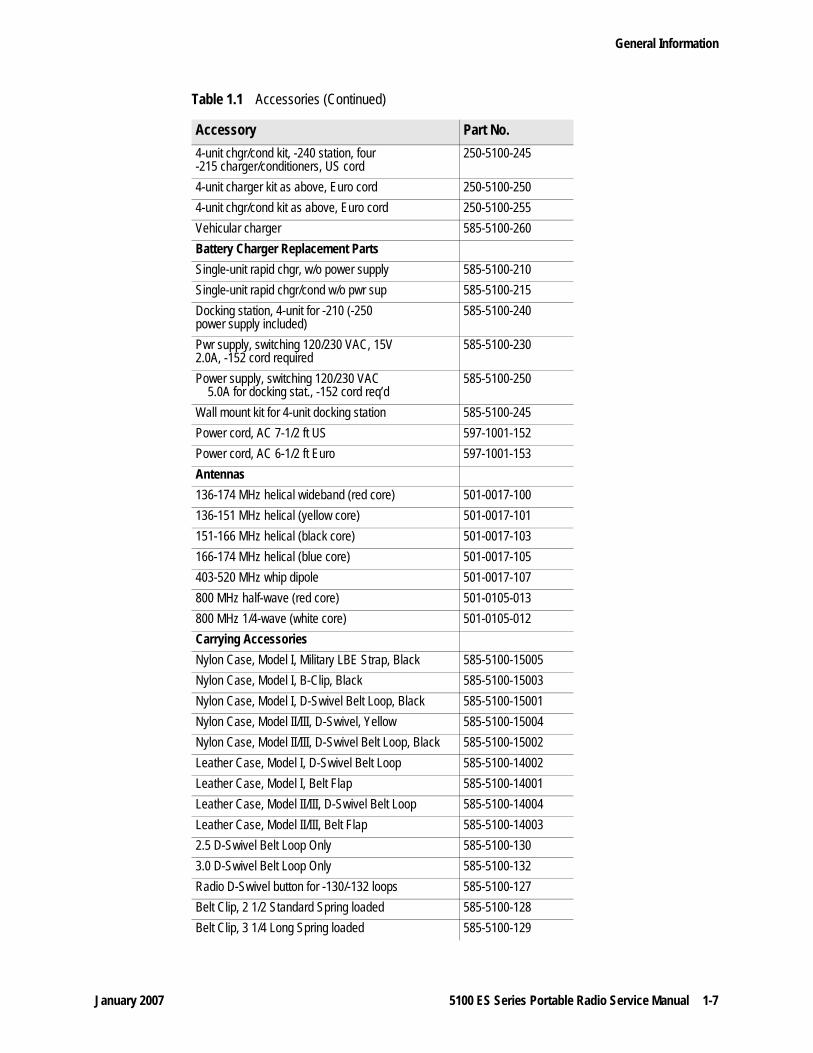
January 2007 5100 ES Series Portable Radio Service Manual 1-7
General Information
4-unit chgr/cond kit, -240 station, four -215 charger/conditioners, US cord
250-5100-245
4-unit charger kit as above, Euro cord 250-5100-2504-unit chgr/cond kit as above, Euro cord 250-5100-255Vehicular charger 585-5100-260Battery Charger Replacement PartsSingle-unit rapid chgr, w/o power supply 585-5100-210Single-unit rapid chgr/cond w/o pwr sup 585-5100-215Docking station, 4-unit for -210 (-250power supply included)
585-5100-240
Pwr supply, switching 120/230 VAC, 15V2.0A, -152 cord required
585-5100-230
Power supply, switching 120/230 VAC 5.0A for docking stat., -152 cord req’d
585-5100-250
Wall mount kit for 4-unit docking station 585-5100-245Power cord, AC 7-1/2 ft US 597-1001-152Power cord, AC 6-1/2 ft Euro 597-1001-153Antennas136-174 MHz helical wideband (red core) 501-0017-100136-151 MHz helical (yellow core) 501-0017-101151-166 MHz helical (black core) 501-0017-103166-174 MHz helical (blue core) 501-0017-105403-520 MHz whip dipole 501-0017-107800 MHz half-wave (red core) 501-0105-013800 MHz 1/4-wave (white core) 501-0105-012Carrying AccessoriesNylon Case, Model I, Military LBE Strap, Black 585-5100-15005Nylon Case, Model I, B-Clip, Black 585-5100-15003Nylon Case, Model I, D-Swivel Belt Loop, Black 585-5100-15001Nylon Case, Model II/III, D-Swivel, Yellow 585-5100-15004Nylon Case, Model II/III, D-Swivel Belt Loop, Black 585-5100-15002Leather Case, Model I, D-Swivel Belt Loop 585-5100-14002Leather Case, Model I, Belt Flap 585-5100-14001Leather Case, Model II/III, D-Swivel Belt Loop 585-5100-14004Leather Case, Model II/III, Belt Flap 585-5100-140032.5 D-Swivel Belt Loop Only 585-5100-1303.0 D-Swivel Belt Loop Only 585-5100-132Radio D-Swivel button for -130/-132 loops 585-5100-127Belt Clip, 2 1/2 Standard Spring loaded 585-5100-128Belt Clip, 3 1/4 Long Spring loaded 585-5100-129
Table 1.1 Accessories (Continued)
Accessory Part No.

1-8 5100 ES Series Portable Radio Service Manual January 2007
General Information
Speaker/Microphones and EarphonesSpkr/mic, coil cord w/2.5mm earphone jk 589-0015-057*Replacement coil cord for above spkr/mic 597-2002-101Earphone kit, coil cord w/2.5mm rt angleplug, for -057 spkr/mic
589-5100-057*
Spkr/mic, public safety, 800 MHz only, 501-0105-012 antenna req’d
589-0015-058*
Earphone kit, coil cord w/2.5mm straightplug, for -057 spkr/mic
589-5100-059*
Earphone adapter, w/3.5 mm thrd jack 589-5100-051*Lightwght headset w/inline PTT for -051 589-0015-059*1-wire earphone kit, for -051 adapter 589-5100-053*2-wire palm mic kit, for -051 adapter 589-5100-055*Programming Accessories5100 Programming Kit (-488 software,-920 cable, CD manual)
250-5100-003
5100 Programming Cable 023-5100-9205100 Cloning Cable 023-5100-930PC Configure programming software, CD 023-9998-488Adapter, DB9M-DB25F 515-9000-015Test Cables and AccessoriesPC Tune radio tuning software 023-9998-499PC Tune cable w/2.5mm audio out jack 023-5100-940Patch cord, 2.5 mm phone plug to BNC 023-5100-9505100 Tuning Kit (-499 software, -940cable, -950 patch cord)
250-5100-005
SMA F to BNC F adapter 515-3102-050UI to Logic Board Test Cable 023-5100-955Encryption Keyloader Accessories SMA (PDA) keyloader 250-5000-945SMA keyloader to 5100 radio cable 023-5000-940SMA keyloader to 5300 radio cable 023-5000-950KVL 3000 keyloader to 5100 radio cable 585-5000-932
Table 1.1 Accessories (Continued)
Accessory Part No.
January 2007 5100 ES Series Portable Radio Service Manual 1-9
General Information
1.6 Intrinsically Safe Information
1.6.1 Introduction
Intrinsically safe 5100 ES transceivers have been approved by the Factory Mutual Research Corporation for operation in certain flammable atmospheres. The specific atmospheres for approved operation are shown in the Section, “Classification of Hazardous Areas and Atmospheres” on page 1-11 and also on the label on the back cover of the transceiver.
When servicing an intrinsically safe transceiver, these rules must be followed to maintain intrinsic safety:
• Service can be provided only by the factory or by service centers specifically authorized by the Factory Mutual Research Corporation to service EFJohnson intrinsically safe transceivers. Contact Factory Mutual at the following address for information concerning their auditing procedure. Contact the EFJohnson Customer Service Depart-ment as described in Section 8.2 if you have questions.
Factory Mutual Research Corporation1151 Boston-Providence TurnpikeP.O. Box 9102Norwood, Massachusetts 02062Phone: (617) 762-4300
• Replace the battery pack only with Intrinsically Safe Battery Pack, Part No. 587-5100-361.
• Do not make any modifications to the circuitry.
• When replacing a part, use only the exact replacement part listed in the service manual parts list.
• Do not install any accessory that is not specifically approved for use with intrinsically safe 5100 ES models. Approved accessories are indicated by an asterisk (*) in the acces-sories listing in Table 1.1.
WARNING!

1-10 5100 ES Series Portable Radio Service Manual January 2007
General Information
1.6.2 Definitions
Intrinsically Safe - This is a fire rating given to these transceivers by the Factory Mutual Research Corporation. When electrical equipment is given this rating, the equipment is considered incapable of releasing sufficient electrical and thermal energy under normal operation or specified fault conditions per the testing standard to cause ignition of a specific flammable or combustible atmosphere in its most easily ignited concentration. In other words, this transceiver should not cause a fire or explosion when used in certain flammable atmospheres.
Fault - A defect or electrical breakdown of any component, spacing, or insulation which alone or in combination with other faults may adversely affect the electrical or thermal characteristics of the intrinsically safe circuit (for example, a shorted transistor).
1.6.3 Possible Ignition Sources
When a transceiver is evaluated by Factory Mutual, possible sources of ignition are checked. These sources may be electrical (spark) or thermal (heat). The following could be sources of spark ignition:
• Discharge of a capacitive circuit by a fault such as a short circuit.• Interruption of an inductive circuit.• Intermittent making or breaking of a resistive circuit.• Hot-wire fusing.• The following could be sources of thermal ignition:• Heating of a small-gauge wire or PC board trace.• High surface temperature of components.
January 2007 5100 ES Series Portable Radio Service Manual 1-11
General Information
1.6.4 Intrinsically Safe and Nonincendive Ratings
This transceiver is rated intrinsically safe for some types of hazards and nonincendive for other types of hazards. An intrinsically safe rating applies to operation in Division 1 areas, and a nonincendive rating applies to operation in Division 2 areas (see next section). The difference between these ratings is as follows:
The intrinsically safe rating is a higher rating because more severe conditions must be met. To be approved for this rating, the transceiver must not cause ignition of a particular atmosphere if two of the faults specified in the testing procedure occur. In other words, it must be able to withstand two simultaneous unrelated breakdowns without causing ignition. To receive a nonincendive rating, the transceiver needs to withstand only a single fault without causing ignition of a particular atmosphere.
1.6.5 Classification of Hazardous Areas and Atmospheres
This transceiver has been submitted for approval to operate in the following hazardous atmospheres and areas. Contact your sales representative or refer to the label on the back of the transceiver to determine the specific atmospheres and areas for which approval was obtained.
Intrinsically Safe - Class I, II, and III, Division 1, Groups C, D, E, F, and G.Nonincendive - Class I, Division 2, Groups A, B, C, and D.Temperature Code - T3C
Definitions of these Class, Division, and Group designations are in the following sections.

1-12 5100 ES Series Portable Radio Service Manual January 2007
General Information
1.6.5.1 Classification of Hazardous Areas (Division)Hazardous areas are classified as Division 1 or 2 as shown in Table 1.2. Since a Division 1 area is considered most hazardous, a transceiver approved for a specific Division 1 atmosphere can also be used in the same Division 2 atmosphere. The intrinsically safe rating applies to Division 1 areas and the nonincendive rating applies to Division 2 areas.
1.6.5.2 Atmosphere Classification (Class/Group)For the purposes of testing and approval, various atmospheric mixtures have been grouped on the basis of their hazardous characteristics. Equipment is approved for a class of material and also for the specific group of gas, vapor, or dust in that class. Class I materials include gases and vapors, Class II materials include combustible dusts, and Class III materials include ignitable fibers or flyings. The typical hazardous materials in each group and class are shown in Table 1.3.
Table 1.2 Area Classification
Division AreaClass I and II Materials (Gases, Vapors, and Dusts)1 An area where there is or could be an explosive
atmosphere most of the time in normal operation2 An area where an explosive atmosphere exists only
as a result of a fault (something going wrong)Class III Materials (Fibers or Flyings)1 An area in which easily ignitable fibers or materials
producing combustible flyings are handled, manufactured, or used.
2 An area in which easily ignitable fibers are stored or handled. An exception is in process of manufacture.
Table 1.3 Material Classification
Typical Hazard Group ClassAcetylene A IHydrogen B IEthylene, ethyl ether, cyclopropane C IGasoline, naphtha, butane, propane, alcohol, acetone, benzol, natural gas
D I
Metal dust including aluminum, magnesium, and their alloys
E II
Carbon black, coal, or coke dust F IIFlour, starch, or grain dusts G IIIgnitable fibers/flyings such as rayon or cotton
- III

January 2007 5100 ES Series Portable Radio Service Manual 1-13
General Information
1.7 Secure CommunicationSecureNet™ and AES voice encryption can be used to provide secure communication with this transceiver. These protocols digitize the voice and then encrypt it using the DES or AES algorithm and an encryption key. The following types of encryption are available on analog and digital channels:
• Analog Conventional and SMARTNET/SmartZone Analog ChannelsDES
• Digital Project 25 and SMARTNET/SmartZone ChannelsDES-OFB (Output Feedback)AES (Advanced Encryption Standard). Refer to the 5100 ES Operating Manual for more information.
• FIPS 140-2 Approved EncryptionDES-OFB and AES encryption is FIPS 140-2 approved in 5100 ES models equipped with the SEM.
• Over-The-Air-Rekeying (OTAR)Encryption keys are loaded into the radio by OTAR (Over-The-Air-Rekeying) using a KMF (Key Management Facility) and/or a handheld keyloader such as the EFJohnson SMA (Subscriber Management Assistant) or Motorola KVL 3000 Plus with the AES option.The keyloader is connected directly to the radio using an interconnect cable, and it loads DES, DES-OFB, and AES keys. Currently, OTAR can be used to load DES-OFB keys on Project 25 conventional channels. Future OTAR of AES keys and on Project 25 trunked channels is planned.
Note Refer to the 5100 ES Operating Manual for more information on OTAR and on secure communication.
1-14 5100 ES Series Portable Radio Service Manual January 2007
General Information
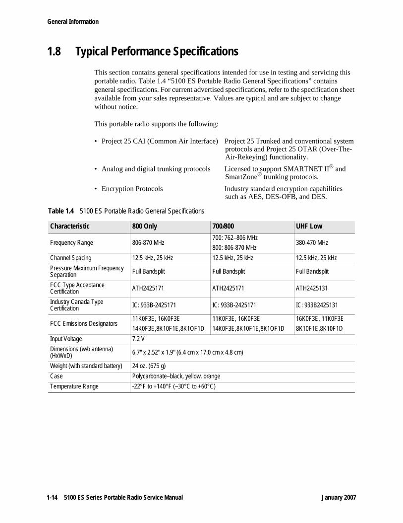
1.8 Typical Performance SpecificationsThis section contains general specifications intended for use in testing and servicing this portable radio. Table 1.4 “5100 ES Portable Radio General Specifications” contains general specifications. For current advertised specifications, refer to the specification sheet available from your sales representative. Values are typical and are subject to change without notice.
This portable radio supports the following:
• Project 25 CAI (Common Air Interface) Project 25 Trunked and conventional system protocols and Project 25 OTAR (Over-The-Air-Rekeying) functionality.
• Analog and digital trunking protocols Licensed to support SMARTNET II® and SmartZone® trunking protocols.
• Encryption Protocols Industry standard encryption capabilities such as AES, DES-OFB, and DES.
Table 1.4 5100 ES Portable Radio General Specifications
Characteristic 800 Only 700/800 UHF Low
Frequency Range 806-870 MHz 700: 762–806 MHz800: 806-870 MHz
380-470 MHz
Channel Spacing 12.5 kHz, 25 kHz 12.5 kHz, 25 kHz 12.5 kHz, 25 kHz Pressure Maximum Frequency Separation Full Bandsplit Full Bandsplit Full Bandsplit
FCC Type Acceptance Certification ATH2425171 ATH2425171 ATH2425131
Industry Canada Type Certification IC: 933B-2425171 IC: 933B-2425171 IC: 933B2425131
FCC Emissions Designators11K0F3E, 16K0F3E14K0F3E,8K10F1E,8K1OF1D
11K0F3E, 16K0F3E14K0F3E,8K10F1E,8K1OF1D
16K0F3E, 11K0F3E8K10F1E,8K10F1D
Input Voltage 7.2 VDimensions (w/o antenna) (HxWxD) 6.7" x 2.52" x 1.9" (6.4 cm x 17.0 cm x 4.8 cm)
Weight (with standard battery) 24 oz. (675 g)Case Polycarbonate–black, yellow, orangeTemperature Range -22°F to +140°F (–30°C to +60°C)
January 2007 5100 ES Series Portable Radio Service Manual 1-15
General Information
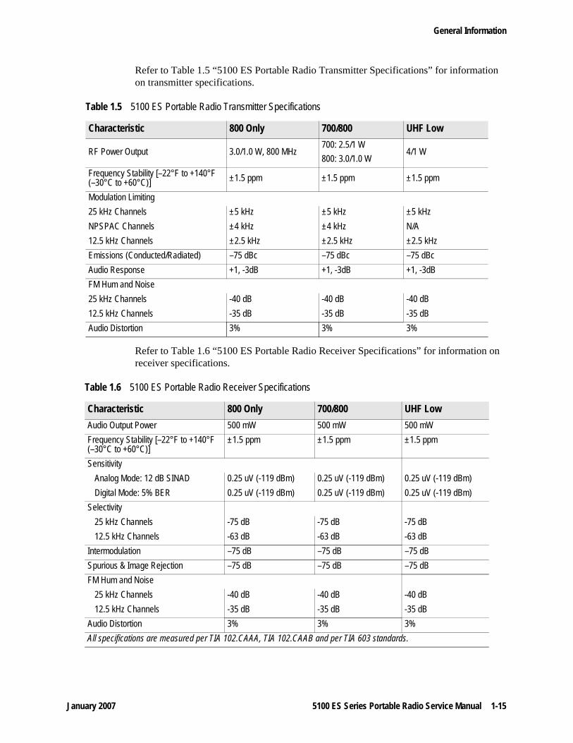
Refer to Table 1.5 “5100 ES Portable Radio Transmitter Specifications” for information on transmitter specifications.
Refer to Table 1.6 “5100 ES Portable Radio Receiver Specifications” for information on receiver specifications.
Table 1.5 5100 ES Portable Radio Transmitter Specifications
Characteristic 800 Only 700/800 UHF Low
RF Power Output 3.0/1.0 W, 800 MHz700: 2.5/1 W800: 3.0/1.0 W
4/1 W
Frequency Stability [–22°F to +140°F (–30°C to +60°C)] ±1.5 ppm ±1.5 ppm ±1.5 ppm
Modulation Limiting25 kHz Channels ±5 kHz ±5 kHz ±5 kHzNPSPAC Channels ±4 kHz ±4 kHz N/A12.5 kHz Channels ±2.5 kHz ±2.5 kHz ±2.5 kHzEmissions (Conducted/Radiated) –75 dBc –75 dBc –75 dBcAudio Response +1, -3dB +1, -3dB +1, -3dBFM Hum and Noise 25 kHz Channels -40 dB -40 dB -40 dB12.5 kHz Channels -35 dB -35 dB -35 dB Audio Distortion 3% 3% 3%
Table 1.6 5100 ES Portable Radio Receiver Specifications
Characteristic 800 Only 700/800 UHF LowAudio Output Power 500 mW 500 mW 500 mWFrequency Stability [–22°F to +140°F (–30°C to +60°C)]
±1.5 ppm ±1.5 ppm ±1.5 ppm
SensitivityAnalog Mode: 12 dB SINAD 0.25 uV (-119 dBm) 0.25 uV (-119 dBm) 0.25 uV (-119 dBm)Digital Mode: 5% BER 0.25 uV (-119 dBm) 0.25 uV (-119 dBm) 0.25 uV (-119 dBm)
Selectivity25 kHz Channels -75 dB -75 dB -75 dB12.5 kHz Channels -63 dB -63 dB -63 dB
Intermodulation –75 dB –75 dB –75 dBSpurious & Image Rejection –75 dB –75 dB –75 dBFM Hum and Noise
25 kHz Channels -40 dB -40 dB -40 dB12.5 kHz Channels -35 dB -35 dB -35 dB
Audio Distortion 3% 3% 3%All specifications are measured per TIA 102.CAAA, TIA 102.CAAB and per TIA 603 standards.
1-16 5100 ES Series Portable Radio Service Manual January 2007
General Information
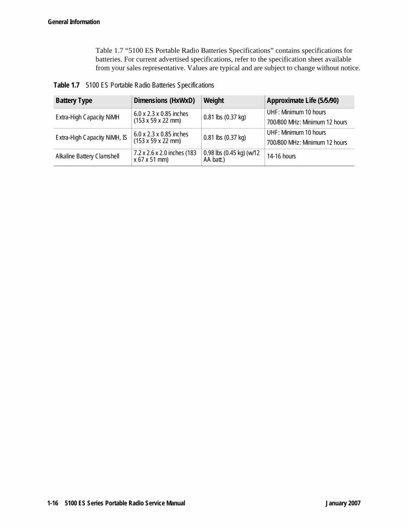
Table 1.7 “5100 ES Portable Radio Batteries Specifications” contains specifications for batteries. For current advertised specifications, refer to the specification sheet available from your sales representative. Values are typical and are subject to change without notice.
Table 1.7 5100 ES Portable Radio Batteries Specifications
Battery Type Dimensions (HxWxD) Weight Approximate Life (5/5/90)
Extra-High Capacity NiMH 6.0 x 2.3 x 0.85 inches (153 x 59 x 22 mm) 0.81 lbs (0.37 kg)
UHF: Minimum 10 hours700/800 MHz: Minimum 12 hours
Extra-High Capacity NiMH, IS 6.0 x 2.3 x 0.85 inches (153 x 59 x 22 mm) 0.81 lbs (0.37 kg)
UHF: Minimum 10 hours700/800 MHz: Minimum 12 hours
Alkaline Battery Clamshell 7.2 x 2.6 x 2.0 inches (183 x 67 x 51 mm)
0.98 lbs (0.45 kg) (w/12 AA batt.) 14-16 hours
January 2007 5100 ES Series Portable Radio Service Manual 2-1
S E C T I O N
Chapter 2Battery, Accessory andDisassembly Information
2.1 Battery Information
2.1.1 Battery Removal/Installation
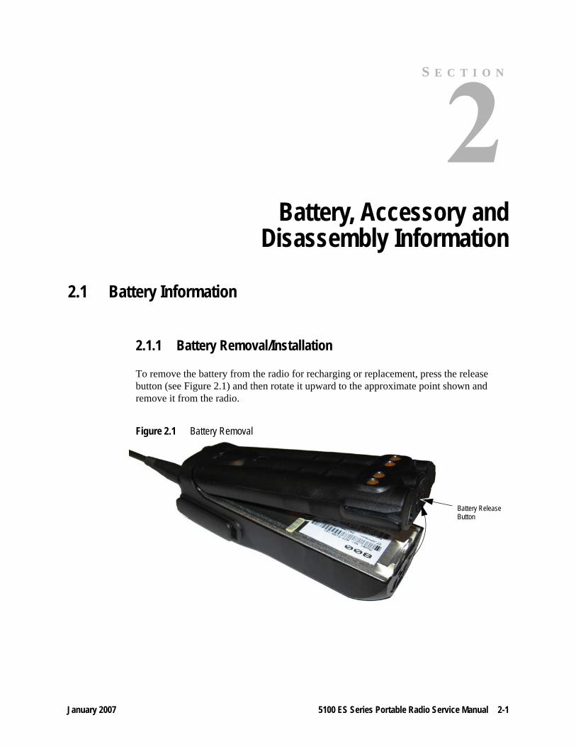
To remove the battery from the radio for recharging or replacement, press the release button (see Figure 2.1) and then rotate it upward to the approximate point shown and remove it from the radio.
Figure 2.1 Battery Removal
Battery ReleaseButton
2-2 5100 ES Series Portable Radio Service Manual January 2007
Battery, Accessory and Disassembly Information
2.1.2 Battery Charging
Note Do not charge the battery with radio power on.
The battery can be charged separately or while attached to the radio. When it is charged while attached to the radio, radio power should be turned off. If it is not, the battery begins slowly discharging when the trickle charge mode is entered. The trickle mode is indicated by a green Ready indication, and it is entered automatically when the battery is nearly fully charged. Gradual discharging occurs in the trickle mode because the charge current of approximately 50 mA is less than the radio standby current of 200 mA.
Do not transmit in close proximity to the charger base.
Do not expose the charger base to high level RF signals while a battery is being charged because this may cause a charger fuse to blow (especially in the UHF range). Radios programmed for SMARTNET/SmartZone operation, for example, may affiliate while in the charger which causes them to key automatically. Therefore, do not leave radio power on while charging as described above.
2.1.3 Preventing Loss of Encryption Keys
If Infinite Key Retention is not programmed, the transceiver must be connected to a constant power source to preserve the encryption keys in memory. Storage capacitors maintain the supply voltage (and these keys) for approximately 30 seconds to allow the battery to be changed. Therefore, when changing the battery of a transceiver containing keys, make sure to reattach another battery within 30 seconds.
Models with Flash code 1.11.0 or later can be programmed for Infinite Key Retention. The keys are then stored in memory and are not lost, even if power is disconnected for an extended period.
2.1.4 Battery Care
Do not incinerate a battery pack because of the risk of explosion. Also, do not short circuit the terminals because the battery pack and the object causing the short may become very hot. Do not disassemble or modify a battery pack.
Proper battery care enhances the useful life of the battery. The battery should be recharged as soon a practical after the low battery indication appears (see Section 3). Follow the charging instructions in the manual included with the charger. When the battery fails to hold a charge or provides only a very short operating time, it must be replaced with a new unit.
A fully charged battery provides approximately 13 hours of service before recharging is required. This time assumes that 5% of the time is spent transmitting, 5% in the receive
CAUTION!
WARNING!

January 2007 5100 ES Series Portable Radio Service Manual 2-3
Battery, Accessory and Disassembly Information
unsquelched mode, and 90% in the receive squelched mode. The operating time may be less if more time is spent in the transmit or unsquelched modes, or if the battery is not fully charged or its capacity has deteriorated. Be sure to dispose of the nickel metal-hydride (NiMH) battery pack in accordance with local waste regulations.
Figure 2.2 Belt Clip Installation
2.2 Belt Clip InstallationRemove the battery and slide the belt clip into the slot on the battery as shown in Figure 2.2. To remove the clip, simply slide it out. It is held in place by the chassis when the battery is installed on the radio.
2.3 Accessory InstallationTo connect an accessory such as a speaker-microphone to the transceiver, refer to Figure 2.3 and proceed as follows:
1 Remove the dust cover over the accessory jack on the side of the transceiver.
2 Insert the hook of the accessory connector into the slot on the side of the transceiver.
3 Hold the latch open, press the connector against the transceiver, and then release the latch to lock the connector in place.
4 Install the included locking screw in the latch tab in the location shown.

2-4 5100 ES Series Portable Radio Service Manual January 2007
Battery, Accessory and Disassembly Information
Figure 2.3 Accessory Installation
2.3.1 Option Select Lines
Opt Sel 1 (pin 1) and Opt Sel 2 (pin 5) of the UDC (accessory) connector indicate to the control logic when an accessory is connected and what accessory is installed. These lines function as follows:
Opt Sel 1 and 2 High (3.3V) - This is the normal operating condition in which no accessory is connected. Both lines are pulled high (3.3V) by internal pull-up resistors.
Opt Sel 1 Low - A speaker-microphone or some other accessory is connected. Opt Sel 2 then functions as an external PTT line (low = PTT), and the radio PTT switch is also functional. The internal speaker and microphone are disabled.
Opt Sel 1 High, Opt Sel 2 Low - The encryption keyloader is connected.
Latch
Install Lock Screw Here
Accessory Connector
Hook
January 2007 5100 ES Series Portable Radio Service Manual 2-5
Battery, Accessory and Disassembly Information
2.4 Transceiver Disassembly
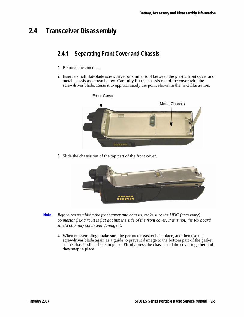
2.4.1 Separating Front Cover and Chassis
1 Remove the antenna.
2 Insert a small flat-blade screwdriver or similar tool between the plastic front cover and metal chassis as shown below. Carefully lift the chassis out of the cover with the screwdriver blade. Raise it to approximately the point shown in the next illustration.
3 Slide the chassis out of the top part of the front cover.
Note Before reassembling the front cover and chassis, make sure the UDC (accessory) connector flex circuit is flat against the side of the front cover. If it is not, the RF board shield clip may catch and damage it.
4 When reassembling, make sure the perimeter gasket is in place, and then use the screwdriver blade again as a guide to prevent damage to the bottom part of the gasket as the chassis slides back in place. Firmly press the chassis and the cover together until they snap in place.
Metal Chassis
Front Cover

2-6 5100 ES Series Portable Radio Service Manual January 2007
Battery, Accessory and Disassembly Information
2.4.2 Removing RF and Logic Boards From Chassis
5 Separate the front cover and chassis as described in the preceding section. The RF and logic boards are located inside the metal chassis as shown below.
6 Remove the shields over the RF and logic boards. These shields insert in slots on one side of the chassis and then clip to the other side of the chassis. These shields also hold the boards in place.
7 Unplug the antenna cable from the RF board using a plier or similar tool at the location shown below. Unlock the logic board flex circuit by sliding the tab on the connector outward. The RF and logic boards can now be removed.
8 When handling these boards, minimize bending of the flex circuit to prevent it from being damaged. Before replacing the RF board, make sure there is adequate heat sink compound on the pad under the RF module.
Logic BoardRF Board
Unlock Flex
Unplug AntJack Cable
Circuit
RF Module
January 2007 5100 ES Series Portable Radio Service Manual 2-7
Battery, Accessory and Disassembly Information
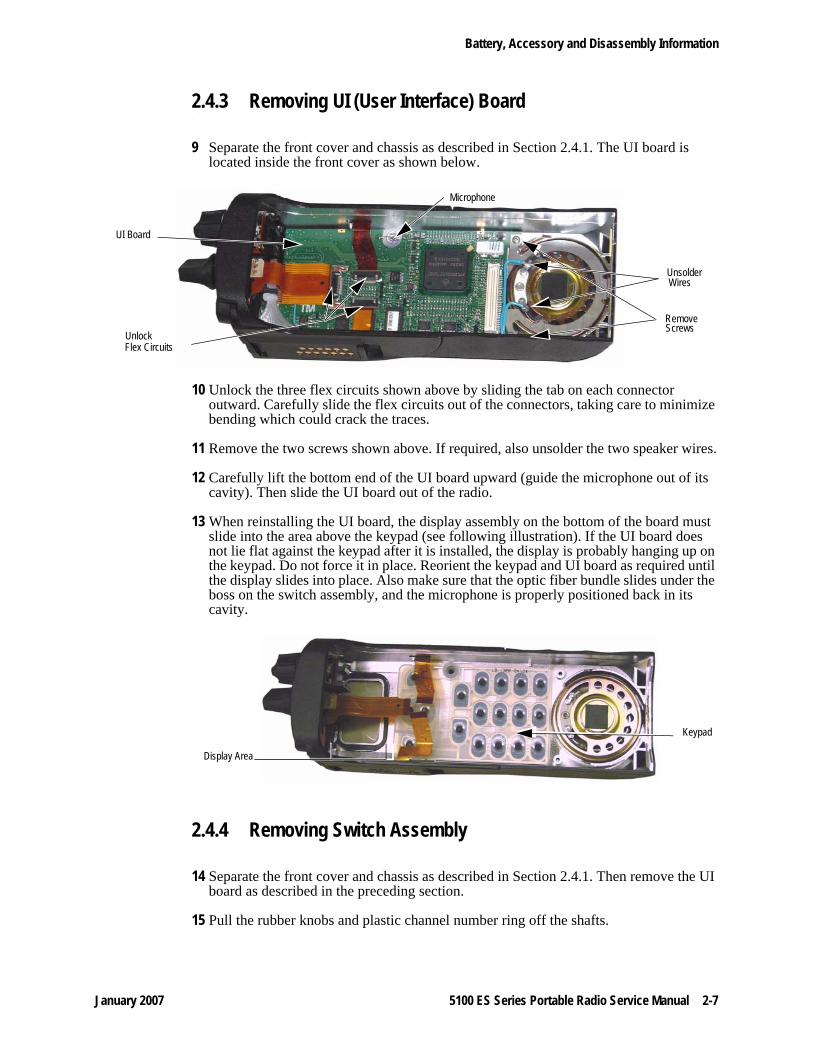
2.4.3 Removing UI (User Interface) Board
9 Separate the front cover and chassis as described in Section 2.4.1. The UI board is located inside the front cover as shown below.
10 Unlock the three flex circuits shown above by sliding the tab on each connector outward. Carefully slide the flex circuits out of the connectors, taking care to minimize bending which could crack the traces.
11 Remove the two screws shown above. If required, also unsolder the two speaker wires.
12 Carefully lift the bottom end of the UI board upward (guide the microphone out of its cavity). Then slide the UI board out of the radio.
13 When reinstalling the UI board, the display assembly on the bottom of the board must slide into the area above the keypad (see following illustration). If the UI board does not lie flat against the keypad after it is installed, the display is probably hanging up on the keypad. Do not force it in place. Reorient the keypad and UI board as required until the display slides into place. Also make sure that the optic fiber bundle slides under the boss on the switch assembly, and the microphone is properly positioned back in its cavity.
2.4.4 Removing Switch Assembly
14 Separate the front cover and chassis as described in Section 2.4.1. Then remove the UI board as described in the preceding section.
15 Pull the rubber knobs and plastic channel number ring off the shafts.
UnlockRemoveScrews
UnsolderWires
Flex Circuits
Microphone
UI Board
Display Area
Keypad
2-8 5100 ES Series Portable Radio Service Manual January 2007
Battery, Accessory and Disassembly Information
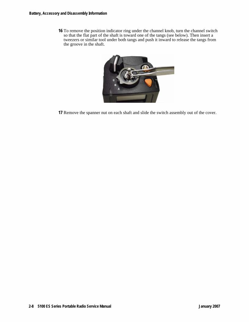
16 To remove the position indicator ring under the channel knob, turn the channel switch so that the flat part of the shaft is toward one of the tangs (see below). Then insert a tweezers or similar tool under both tangs and push it inward to release the tangs from the groove in the shaft.
17 Remove the spanner nut on each shaft and slide the switch assembly out of the cover.
January 2007 5100 ES Series Portable Radio Service Manual 3-1
S E C T I O N
Chapter 3Operation
3.1 GeneralThe operation of the 5100 ES transceiver is described in the 5100 ES Model I Operating Manual and the 5100 ES Model II/III Operation Manual. These manuals are available from your EFJohnson dealer.

3-2 5100 ES Series Portable Radio Service Manual January 2007
Operation
January 2007 5100 ES Series Portable Radio Service Manual 4-1
S E C T I O N
Chapter 4Transceiver Programming
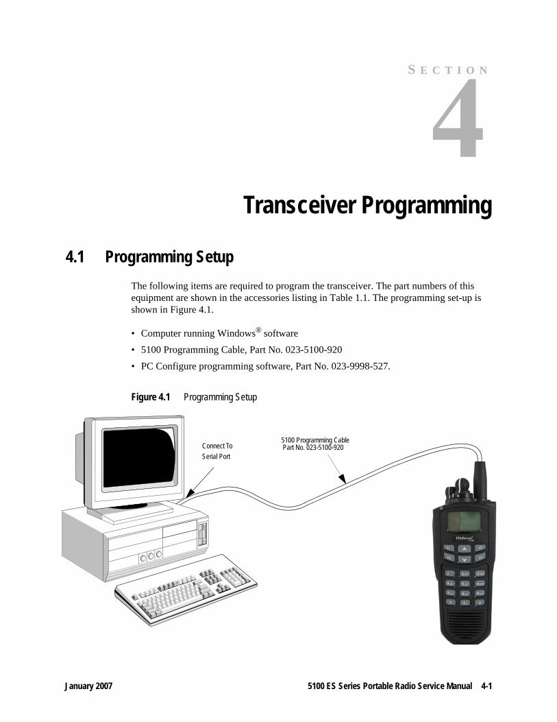
4.1 Programming SetupThe following items are required to program the transceiver. The part numbers of this equipment are shown in the accessories listing in Table 1.1. The programming set-up is shown in Figure 4.1.
• Computer running Windows® software• 5100 Programming Cable, Part No. 023-5100-920• PC Configure programming software, Part No. 023-9998-527.
Figure 4.1 Programming Setup
5100 Programming CableConnect ToSerial Port
Part No. 023-5100-920
4-2 5100 ES Series Portable Radio Service Manual January 2007
Transceiver Programming
Note The 023-5100-920 cable, 023-9998-527 software, and a CD manual are included in the 5100 ES Portable Radio Programming Kit, Part No. 250-5100-003.
4.2 Computer DescriptionThe computer used to run this program should meet the following minimum requirements:
• Windows 2000 or XP• Pentium® processor or equivalent• A hard disk drive with at least 4 MB of free space• A CD-ROM drive• An available serial port
4.3 Using the PC Configure Software The PC Configure software is described in a separate manual included on the PC Configure CD.
Tone (CTCSS) and digital (DCS) Call Guard tones and 800 Mhz channel frequencies are located in the back of the above manual.
4.4 Firmware Upgrade Instructions
4.4.1 Upgrade Utility Compatibility
PC Configure 2.4.x supports 5100 ES Portable Radios that have 4.8.x firmware. This firmware has a revised memory configuration for storing the radio operating program. Firmware versions utilizing this new memory configuration are as follows:
Non-SEM - Version 1.14.0 or laterSEM - Version 2.04.0 or later
A new utility is required to upgrade the radio firmware. This utility is included in PC Configure™ Version 1.24.0 or later. This utility is not compatible with earlier versions of firmware. Additional information follows:
• To upgrade radios to the above firmware versions or later, PC Configure Version 1.24.0 or later must be used.
• To upgrade radios to earlier versions than those shown above, PC Configure Version 1.22.0 or earlier must be used.

January 2007 5100 ES Series Portable Radio Service Manual 4-3
Transceiver Programming
• If an attempt is made to upgrade firmware with the wrong version of PC Configure software, the procedure halts and an error message is displayed.
• When upgrading early versions of firmware to one of the preceding versions or later, the Boot Loader code must also be updated. This must be done before updating the main PPC code.
• This limitation does not apply to standard programming of radio personality parameters. The PC Configure software is backward compatible and can be used to program radios with earlier versions of firmware. However, some parameters may not be available with earlier versions of firmware.
4.4.2 Firmware Upgrade instructions
Note If upgrading to the version of firmware described in the preceding section, the Boot Code must also be upgraded, and it must be done before upgrading the PPC code.
4.4.2.1 Requirements
4.4.2.1.1 Firmware Versions
Note The firmware (Flash/operating software) version number is briefly displayed when the radio powers up. It is also indicated by the 13th digit of the radio part number (242-51xx-xxx-xxV).
Three different logic versions of the 5100 ES portable are in service, and each uses a different code base as follows. The same code base must be used to upgrade the firmware. For example, if the radio currently has Ver 3.1.0, the new code must have a 3.x.x version number, not 2.x.x. or 1.x.x.
Code Version Displayed Radio Version
Version 1.x.x Standard Version
Version 2.x.x SEM Version
Version 3.x.x UCM Version

4-4 5100 ES Series Portable Radio Service Manual January 2007
Transceiver Programming
4.4.2.1.2 Equipment Required
4.4.2.2 PC Configure Upgrade Instructions After installing a new version of PC Configure, be sure to transfer the system key and data files as described below. Previous PC Configure versions can then be safely uninstalled if desired (although a previous version does not need to be removed to run a new version).
1 Install the new version of the PC Configure programming software on your computer’s hard drive. The default location of this software is C:\Program Files\EF Johnson\PC Configure.
2 Using the Windows® File Explorer application, copy the system key and data files from
the previous PC Configure “Data” and “Keys” folders to the same folders of the new PC Configure version.
4.4.2.3 Initial Setup
1 Connect the programming cable to the serial port of your computer. Remove the accessory/programming jack cover on the side of the 5100 ES radio and connect the other end of the programming cable to this jack.
2 Start the PC Configure program.
3 From PC Configure, open the Radio menu and select Series > “5100 Portable”. Then open the Transfer menu and select Baud Rates > “115200” baud.
Note If a communication error occurs, try selecting a lower baud rate.
4 From PC Configure, verify the current code version by opening the Transfer menu and selecting Read Version Info from Radio. Note the Controller Version number in the window that is displayed. This indicates what code base version to use. For example, if the radio currently has Ver 4.8.x, the new code must have a 4.x.x version number.
5 Using the Windows File Explorer application, copy the code file “Ver_0x_xx_xx.hex” on the included CD-ROM to the PPC\5100 folder under the new version of PC Configure located at C:\Program Files\EF Johnson\PCConfigure.
6 If new Boot code is also included, copy the “CodeDownLoadROM_1_x.hex” file on the included CD-ROM to the PPC\5100\Upgrade folder under the new version of PC Configure located at C:\Program Files\EF Johnson\PCConfigure.
Description Part No.PC Configure Software on CD-ROM 023-9998-527 Windows®-Based Computer -5100 Programming Cable 023-5100-920
CAUTION!
January 2007 5100 ES Series Portable Radio Service Manual 4-5
Transceiver Programming
4.4.2.4 Firmware Upgrade Procedure
Note Radio personality programming previously performed using the PC Configure software is not changed when the firmware is updated as follows. Any encryption keys in the 5100 radio will be lost and must be reloaded.
4.4.2.4.1 Boot Code Downloading (If Supplied)
Note The radio must be connected to the computer before performing this step.
1 Open the Transfer menu and select Write Application Code To Radio. The Password is then requested. Enter wildcats using lowercase letters and click the OK button.
2 Verify “Loader file to Download” has the file “5100PCConifBootUpgradeLoader.hex” selected. If not, click the “Choose” button and select this file in PPC\5100\upgrade folder.
3 Click the “Choose” (Code) button to the right of the “Code file to Download” box and select the upgrade file “CodeDownLoadROM_x_x.hex” that you copied in the initial setup to the PPC\5100\Upgrade folder.
4 With the 5100 radio powered off, select the bootload (code programming) mode by pressing and holding the third side option button immediately above the PTT switch and then turn power on. Release the button and the display will indicate “Bootload Waiting for serial-bus command.”
5 Click the “Start” button and the progress bar should begin advancing to the right. If downloading does not start, wait until the “Communication Problem During Code Download” message appears and then click “Start” again. Typically, if a sync failure occurs on the first attempt, it will not be successful until the third or fourth attempt. Download time varies with the speed of your computer and serial port card.
6 When downloading is complete, the 5100 radio does not automatically cycle power. Manually turn power off and then on.
7 Click the OK button.
4.4.2.4.2 PPC Code Downloading
1 Open the Transfer menu and select Write Application Code To Radio. The Password is then requested. Enter huskers using lowercase letters and click the OK button.
2 Click the “Choose” (Code) button at the right end of the “Code file to Download” box and select the upgrade file “Ver_0x_xx_xx.hex” that you copied in the initial setup to the PPC\5100 folder.
3 With the 5100 powered off, select the bootload (code programming) mode by pressing and holding the third side option button immediately above the PTT switch and then turn power on. Release the button and the display will indicate “Bootload Waiting for serial-bus command.”
4-6 5100 ES Series Portable Radio Service Manual January 2007
Transceiver Programming
4 Click the “Start” button and the progress bar should begin advancing to the right. If downloading does not start, wait until the “Communication Problem During Code Download” message appears and then click “Start” again. Typically, if a sync failure occurs on the first attempt, it will not be successful until the third or fourth attempt. Download time varies with the speed of your computer and serial port card.
5 When downloading is complete, radio power automatically cycles. If the error “BAD FL FMT” appears in the 5100 display, the programming file was created with an older version of PC Configure. To correct this error, read the programming file from the radio and then write it back again.
6 Click the OK button to exit the Write Application Code to Radio window.
7 Once a 5100 radio has been upgraded, Read and then Write the programming file to correct any differences in PC Configure versions. To do this, open the Transfer menu and select Read Parameters from Radio. The Progress bar at the bottom of the programmer advances as the parameters are read. Radio power automatically cycles after this occurs.
8 Wait for the power to cycle and the radio to return to the normal mode. Then open the Transfer menu and select Write Parameters to Radio. The Progress bar at the bottom of the screen advances as the parameters are written. Radio power automatically cycles after the parameters are written.
9 To verify that the new code version has been loaded, open the Transfer menu and select Read Version Info From Radio. Note the Controller Version number to verify that the new code version has been loaded. Click the OK button.
10 If “Parms Fail” is displayed by the radio, a programming parameters error was detected during the self-test part of the power-up cycle. To correct this error, Read and then Write the programming file again.
11 To upgrade another radio, repeat this procedure starting with step 1.
12 If you are upgrading a large number of radios and do not need to distribute them immediately, you can stop at step 5 and return to step 3.
13 If encryption keys were in the 5100 radio prior to this upgrade, these keys should now be reloaded.
4.5 Cloning ProcedureThe Clone feature allows one radio to be used to program another with identical information. The PC Configure programming software is not required. Only conventional analog and Project 25 zones can be programmed with this feature. SMARTNET/SmartZone and Project 25 trunked information is not transferred. The Clone option switch must be programmed on the master radio. With the latest 5100 versions, both wireless and wired cloning are available.
For more information on cloning one radio with another, refer to the PC Configure Programming Manual.

January 2007 5100 ES Series Portable Radio Service Manual 5-1
S E C T I O N
Chapter 5Circuit Description
5.1 General Overview
5.1.1 Introduction
The EFJohnson 5100 ES Portable Radio uses a PowerPC®-based controller and a Digital Signal Processor (DSP) to provide the following modes of operation:
Narrowband Analog - FM modulation with a maximum deviation of 2.5 kHz. This mode is usually used in systems where the channel spacing is 12.5 kHz. Call Guard (CTCSS or DCS) subaudible squelch signaling can be used in this mode.
Wideband Analog - FM modulation with a maximum deviation of 5 kHz. This mode is usually used in systems where the channel spacing is 25 kHz or 30 kHz. Call Guard (CTCSS or DCS) subaudible squelch signaling can be used in this mode.
Project 25 Digital - The voice is digitized, error corrected, optionally encrypted and transmitted using C4FM modulation according to the Project 25 standard. This mode can be used in channel spacings of 12.5 kHz.
The DSP processes the received signals and generates the appropriate output signals. The microcontroller controls the hardware and provides an interface between hardware and DSP.
5.1.1.1 PC BoardsThis radio contains the following PC boards:
• RF Board• Logic Board

5-2 5100 ES Series Portable Radio Service Manual January 2007
Circuit Description
• User Interface (UI) Board• Five flex circuits that provide interconnection with the RF board, display, top panel
controls, side buttons, and UDC (accessory) connector.The UI Board provides the input/output interface for the user. It contains the PowerPC processor which is the main controller for the transceiver. It also contains the keypad and has inputs for the various buttons and switches. It also controls the display and performs all RS-232 communications between the radio and remote computer stations for the purposes of radio programming, tuning, encryption key loading and software downloading.
The Logic Board contains the digital audio processing circuitry that includes the CODEC and DSP devices.
5.1.2 Analog Mode
5.1.2.1 Receive ModeThe signal is routed from the antenna connector to the RF Board where it is filtered, amplified, and mixed with the first local oscillator frequency generated by the synthesizer. The resulting IF signal is also filtered and amplified and sent to the AD9864 digital IF chip.
The signal is then mixed with the second local oscillator frequency to create a second IF signal. The second IF signal is then sampled and downconverted to baseband. The baseband signal is then decimated to a lower sample rate that is selectable at 20 kHz. This signal is then routed via a serial interface from the IF chip to the DSP on the logic board.
On the logic board the DSP digitally filters the input signal and performs frequency discrimination to obtain the message signal. The DSP first performs a carrier-detection squelch function on the radio. If a signal is determined to be present, the audio portion of the signal is resampled and then filtered appropriately. The filtered signal is then routed back to a D/A in the CODEC to produce an analog signal for output to the audio power amplifier and then the speaker. Any detected signaling information is decoded and the resulting information is sent to the microcontroller.
5.1.2.2 Transmit ModeThe signal from the microphone is amplified and then routed to the CODEC chip where it is first digitized and then sent to the DSP. The DSP performs the required filtering, adds the desired signaling, converts the sample rate and then sends the resulting signal back to a D/A in the CODEC to produce the analog modulation signals for the VCOs. The modulated VCO signal is then sent to the RF power amplifier and transmitted.

January 2007 5100 ES Series Portable Radio Service Manual 5-3
Circuit Description
5.1.3 Project 25 Digital Mode
In Project 25 Digital Mode, the carrier is modulated with four discrete deviation levels. These levels are ± 600 Hz and ± 1800 Hz. Digitized voice is created using an IMBE™ vocoder.
5.1.3.1 Receive ModeThe signal is processed in the same way as an analog mode transmission until after the squelch function is performed. If a signal is detected to be present, the DSP resamples the signal from 20 kHz to 24 kHz. This is done so that the sample rate is an integer multiple (5x) of the data rate of the digital modulation which is 4800 symbols/sec (9600 bits/sec).
The resampled signal is then processed by a demodulator routine to extract the digital information. The resulting bit stream (9600 bps) is sent to a routine that performs unframing, error-correction, and voice decoding. The result of these operations is a reconstructed voice signal sampled at 8 kHz. The sampled voice signal is sent to a D/A in the CODEC to produce an analog signal for output to the audio power amplifier and speaker.
5.1.3.2 Transmit ModeThe microphone signal is processed as in the analog mode until it reaches the DSP. At this point the audio signal is processed by a voice encoding routine to digitize the information. The resulting samples are then converted to a bit stream that is placed into the proper framing structure and error protected. The resulting bit stream has a bit rate of 9600 Hz.
This bit stream in then encoded, two bits at a time, into a digital level corresponding to one of the four allowable frequency deviations. This produces 16-bit symbols with a rate of 4800 Hz. The symbols are resampled to a rate of 48 kHz and filtered to comply with channel bandwidth requirements. The filtered signal is then sent to a D/A in the CODEC to produce the analog modulation signal for the VCO. The modulated VCO signal is then mixed up to the final transmit frequency and then sent to the RF PA for transmission.
5.2 UHF Low RF Board
Note The RF Board is not field serviceable. It must be replaced as a unit with a new board.
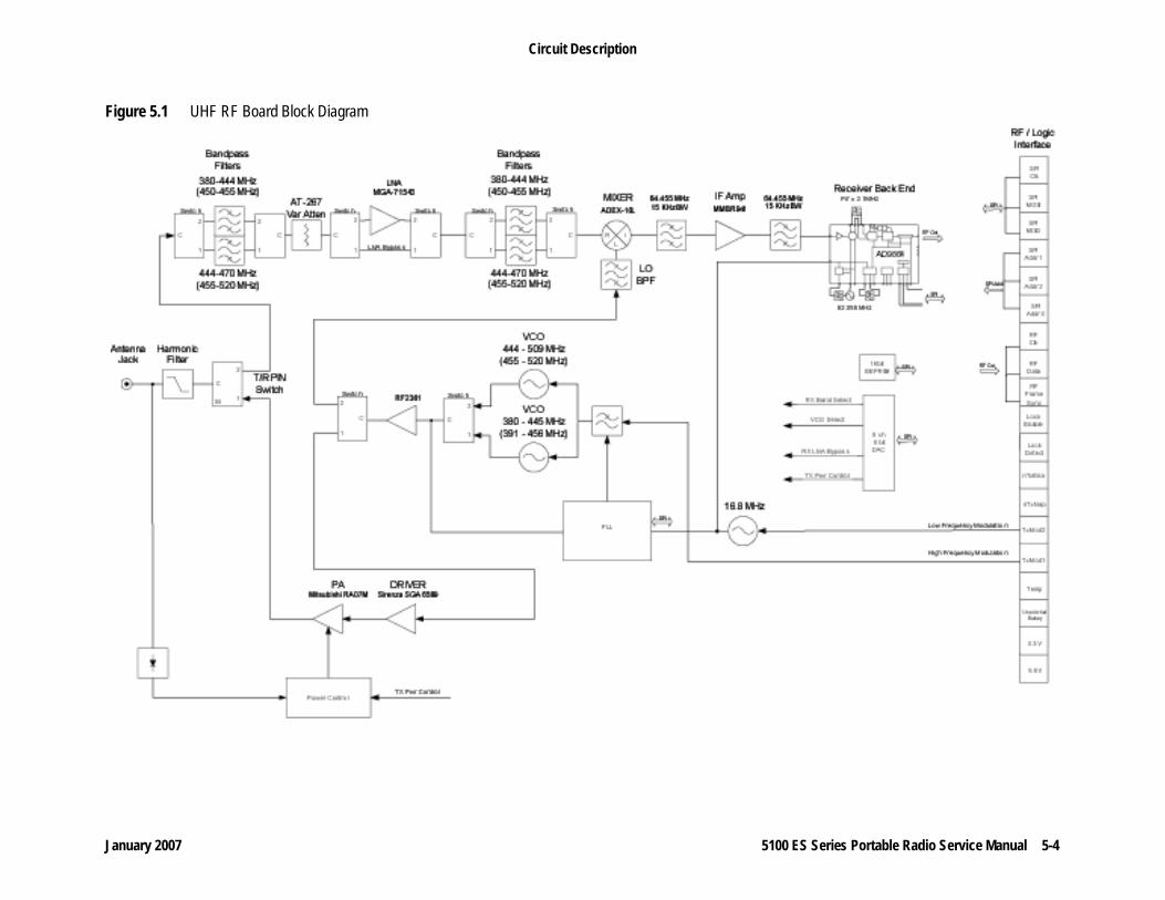
January 2007 5100 ES Series Portable Radio Service Manual 5-4
Circuit Description
Figure 5.1 UHF RF Board Block Diagram

January 2007 5100 ES Series Portable Radio Service Manual 5-5
Circuit Description
5.2.1 Receiver
5.2.1.1 Front End Bandpass FilterA harmonic filter is followed by a PIN diode transmit/receive switch. Following the switch, two fixed tuned bandpass filters are used in the front-end of the receiver. Depending on the desired receive band, the appropriate filter is selected using RF switches (U37/U41). This filter provides first-image rejection with minimal loss in order to provide the desired level of receiver sensitivity. A variable attenuator, which follows the filter, increases the dynamic range of the receiver when receiving high-level signals.
5.2.1.2 Front End LNA and Bypass SwitchingThe Low Noise Amplifier (LNA) is critical in determining the overall noise figure of the receiver chain. An MGA-71543 amplifier (U39) provides optimum noise figure, gain, intercept point, and power consumption.
5.2.1.3 Post-LNA Bandpass FiltersAdditional bandpass filters are positioned after the LNA. These filters are identical to the front-end filters previously described. RF switches U42 and U40 are used to select between the two bands. These filters provide additional image rejection.
5.2.1.4 Mixer and LO FilterA double-balanced, low-level ADEX-10L mixer (MX1) with a LO drive level of +4 dBm is used for the first conversion. This mixer provides good dynamic range with a 3 dB lower LO drive than the more traditional +7 dBm drive mixers. This reduces power consumption and also the conducted and radiated local oscillator leakage from the receiver.
For the low band UHF version, a high-side mix is used for the 380-444 MHz receive band and a low-side mix is used for the 444-470 MHz receive band. For the high band UHF version, a high-side mix is used for the 450-455 MHz receive band and a low-side mix is used for the 455-520 MHz receive band. This band plan reduces the tuning range requirements for the VCOs.
A LO filter is used prior to LO port of the mixer to reduce the impact of wideband noise from the LO synthesizer on the receiver sensitivity.
5.2.1.5 IF Filter and AmplifierA two-pole 64.455 MHz crystal filter (U2) is used to provide the desired level of adjacent channel rejection while providing minimal amplitude and phase distortion within a 25
5-6 5100 ES Series Portable Radio Service Manual January 2007
Circuit Description
KHz bandwidth. Shields installed around the crystal filter provide sufficient isolation to meet the second image response specifications and minimize noise pickup by the impedance-matching inductors (L1, L2, L3, L4 and L7.)
A transistor IF amplifier (Q1 and supporting circuitry) is required to boost the signal strength, thereby reducing the overall noise figure. The noise figure, signal gain, intercept point, and power consumption are optimized in this design. An additional two-pole 64.455 MHz crystal filter (U25) is used to increase the adjacent channel rejection. An LC circuit provides the required impedance matching between the output of the IF filter and the input of the backend chip (U11.)
5.2.1.6 Back End ICAn Analog Devices AD9864 IF Digitizing Subsystem IC (U11) provides a variety of functions for the receiver as follows:
Second Local Oscillator - A varactor-tuned transistor (Q2) oscillator is phase-locked to a fixed frequency of 62.355 MHz for converting the first IF of 64.455 MHz to a second IF frequency of 2.1 MHz. Phase Locked Loop circuitry inside of the AD9864 operates with a phase-detector frequency of 15 kHz.Second Conversion Mixer and Filtering - A mixer inside the AD9864 converts from the first IF of 64.455 MHz to the second IF of 2.1 MHz. External filters (L29 and L30) provide IF bandpass filtering. Additional filtering is provided by the inherent operation of the sigma-delta analog/digital converters.Gain Control - This device provides up to 12 dB of AGC range via a combination of analog and digital controls. Additionally, there is a 16 dB attenuator in the front end. The optimum settings are controlled by the host microprocessor.Analog / Digital Conversion and Processing - Sigma-delta converters provide I and Q sampling directly from the second IF frequency. The resulting digital words are first filtered by internal programmable FIR filters and then clocked out of the AD9864 via a serial data bus using a programmable data rate.
5.2.2 Synthesizer
5.2.2.1 PLL ICA CX72301 sigma-delta modulated PLL (U29) forms the basis of the main synthesizer that is used for both receive and transmit modes. This PLL chip provides good phase noise capabilities to reduce adjacent channel interference and quick switching between the receive and transmit modes.
In receive mode the PLL is programmed for a local oscillator frequency that is 64.455 MHz away from the receive frequency. In transmit mode the PLL is programmed directly for the transmit frequency.

January 2007 5100 ES Series Portable Radio Service Manual 5-7
Circuit Description
5.2.2.2 Reference OscillatorA 16.8 MHz oscillator (Y1) is used as the frequency reference to the synthesizer and also to the receiver backend IC. The center frequency of this oscillator is corrected using a DC tuning voltage from the digital board during receive and voice and data modulation during transmit.
5.2.2.3 Analog Switches and PLL Loop FiltersAn analog switch (U17) provides quicker switching of signals during channel changes by varying the time constant of the PLL loop filter.
5.2.2.4 VCOsTwo different VCOs minimize the tuning range of the VCOs in order to meet phase noise specifications. Both VCO's (U1 and U5) are used for transmit and receive modes. Their combined tuning range covers the entire transmit and receive frequency bands. Transmit modulation is provided to each oscillator's modulation port from the digital board.
A RF2361 buffer amplifier (U6) provides the required level of drive for the receiver mixer's local oscillator signal as discussed above.
5.2.3 Transmitter
5.2.3.1 ModulationA “dual-port” modulation scheme is used in order to provide DC coupling of the signal required for data modulation applications. Modulation applied to the PLL's frequency reference provides low-frequency modulation, whereas modulation applied to the PLL's transmit VCO's (U1 and U5) provide high-frequency modulation. Signals for both modulation ports are provided from DACs on the digital board.
5.2.3.2 Power AmplifierThe power amplifier (U3) is a Mitsubishi RA07M4047M-01 module for the low band version and a Mitsubishi RA07M4452M-01 module for the high band version. The PA module provides the desired RF power output level and is stable over a wide range of VSWR conditions. The PA is driven by a SGA-6589 driver (U20) that typically provides +21 dBm output power. The PA is turned on and off by switching the power to this driver via transistor D10.

5-8 5100 ES Series Portable Radio Service Manual January 2007
Circuit Description
5.2.3.3 ALCTo maintain the specified Transmitter output power level, Automatic Level Control (ALC) is provided to control the drive level to the PA. The detected forward power is compared to a reference level provided by the digital board via op amp U21A. The resulting error voltage is applied to a power level control port of the power amplifier module. Transmitter on/off splatter filtering is provided by an RC network (R76, R109, C267 and C141.)
5.2.3.4 T/R Switching and Harmonic FilterThe output of the power amplifier is applied to the transmit/receive RF PIN switch (D12 & D13.) This is a high dynamic-range switch that is capable of passing the desired transmit power with minimal compression. Any harmonics generated by the PA module and the RF T/R switch are filtered by a harmonic filter that is between the RF T/R switch and the antenna jack.
5.3 700/800 MHz RF Board
Note The RF Board is not field serviceable. It must be replaced as a unit with a new board.
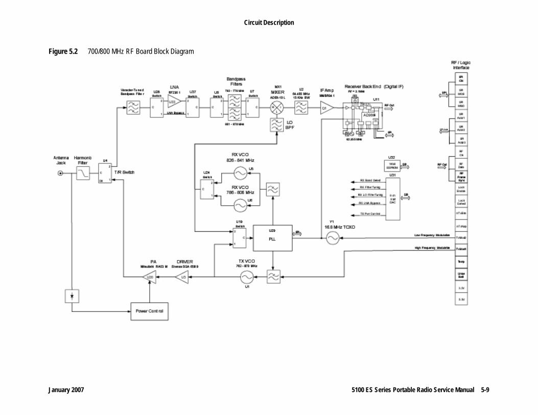
January 2007 5100 ES Series Portable Radio Service Manual 5-9
Circuit Description
Figure 5.2 700/800 MHz RF Board Block Diagram

5-10 5100 ES Series Portable Radio Service Manual January 2007
Circuit Description
5.3.1 Receiver
5.3.1.1 Front End Bandpass FilterA varactor-tuned bandpass filter (including W3 and W4) is used in the front-end of the receiver. This filter provides first-image rejection with minimal loss to provide the desired level of receiver sensitivity. The front-end bandpass filter center frequency is tuned via voltages from an 8-channel D/A converter. Ceramic resonators provide a high circuit Q and lower loss than a fixed inductor. A back-to-back varactor diode configuration increases the circuit's third-order intercept point.
5.3.1.2 Front End LNA and Bypass SwitchingLow Noise Amplifier (LNA) U33 is critical in determining the overall noise figure of the receiver. The RF2361 amplifier provides a good noise figure, gain, intercept point and power consumption. RF switches U28 and U37 bypass the signal around the LNA when required to increase the effective third-order intercept point and the interference rejection capabilities of the receiver.
5.3.1.3 Post-LNA Bandpass FiltersAdditional bandpass filters are used after the LNA. These filters are fixed-tuned since varactor-tuned filters would have an excessive third-order intercept point. One filter bank is tuned to the 700 MHz receive band and the other bank to the 800 MHz receive band. RF switches U8 and U7 select the desired band. These filters have better selectivity and more loss than the front-end filters, but the gain of the LNA minimizes the impact of the filter loss on the receiver sensitivity.
5.3.1.4 Mixer and LO FilterA double-balanced, low-level ADEX-10L mixer (MX1) with a LO drive of +4 dBm is used for the first conversion. This mixer provides good dynamic range with 3 dB lower LO drive than the more traditional +7 dBm drive mixers. This provides power savings and reduces conducted and radiated LO leakage from the receiver. A high-side mix is used for the 700 MHz receive band and a low-side mix is used for the 800 MHz receive band. This band plan reduces the tuning range requirements for the VCOs.
A LO filter (including W1 and W2) is used prior to LO port of the mixer to reduce the effect of wideband noise from the LO synthesizer on the receiver sensitivity. This filter is varactor-tuned with the center frequency tuned via a voltage from a D/A converter.
January 2007 5100 ES Series Portable Radio Service Manual 5-11
Circuit Description
5.3.1.5 IF Filter and AmplifierA four-pole 64.455 MHz crystal filter (U2) is used to provide the desired level of adjacent channel and image rejection while providing minimal amplitude and phase distortion within the 25 kHz bandwidth. Shields are installed around the crystal filter to provide sufficient isolation in order to meet the second image response requirements and minimize noise pickup by the impedance-matching inductors (L1, L2 and L7.)
A transistor IF amplifier (Q1 and supporting circuitry) is used to boost the signal strength which reduces the overall noise figure. The noise figure, signal gain, intercept point and power consumption are optimized by this circuit. An LC circuit provides the required impedance matching between the output of the IF amplifier and the input of backend chip U11.
5.3.1.6 Back End ICAn Analog Devices AD9864 IF Digitizing Subsystem IC (U11) provides the following receiver functions:
Second Local Oscillator - A varactor-tuned transistor (Q2) oscillator is phase-locked to a fixed frequency of 62.355 MHz in order to convert the first IF of 64.455 MHz to a second IF frequency of 2.1 MHz. Phase Locked Loop circuitry inside of the AD9864 operates with a phase-detector frequency of 15 kHz.Second Conversion Mixer and Filtering - A mixer inside the AD9864 converts from the first IF of 64.455 MHz to the second IF of 2.1 MHz. External filters L29 and L30 provide IF bandpass filtering. Additional filtering is provided by the inherent operation of the sigma-delta analog/digital converters.Gain Control - This device provides up to 12 dB of AGC range via a combination of analog and digital controls. Additionally, there is a 16 dB attenuator in the front end. The optimum settings are controlled by the host microprocessor.Analog/Digital Conversion and Processing - Sigma-Delta Converters provide I and Q sampling directly from the second IF frequency. The resulting digital words are first filtered by internal programmable FIR filters and then clocked out of the AD9864 via a serial data bus using a programmable data rate.

5-12 5100 ES Series Portable Radio Service Manual January 2007
Circuit Description
5.3.2 Synthesizer
5.3.2.1 PLL ICA CX72301 sigma-delta modulated PLL (U29) is used as the main receive and transmit synthesizer. This PLL chip provides exceptional phase noise capabilities to reduce adjacent channel interference and quick switching between the receive and transmit modes.
In the receive mode the PLL is programmed to a Local Oscillator frequency that is 64.455 MHz from the receive frequency. For the 700 MHz receive band, the LO frequency is higher than the receive frequency, and for the 800 MHz band, it is lower than the receive frequency. In transmit mode, the PLL is programmed directly to select the desired transmit frequency.
5.3.2.2 Reference OscillatorA 16.8 MHz oscillator (Y1) provides the frequency reference for the synthesizer and receiver backend IC. The center frequency of this oscillator is corrected using a DC tuning voltage from the digital board during receive and it is modulated with voice or data during transmit.
5.3.2.3 Analog Switches and PLL Loop FiltersAnalog switches U16, U17, and U18 provide faster channel switching by changing the time constant of the PLL loop filters.
5.3.2.4 VCOsThree different VCOs are used. VCO U1 is used strictly in transmit mode. It's tuning range covers the entire transmit and receive frequency bands. Transmit modulation is provided to this oscillator's modulation port from the digital board through R9.
Two receive VCOs (U5 and U6) are required to meet the phase noise requirements. Each VCO functions for only one of the two receive bands. An RF2361 buffer amplifier (U40) provides the required level of drive for the receiver mixer's local oscillator signal as discussed above.

January 2007 5100 ES Series Portable Radio Service Manual 5-13
Circuit Description
5.3.3 Transmitter
5.3.3.1 ModulationA “dual-port” modulation scheme is used to provide DC coupling of the signal for data modulation applications. Modulation applied to the PLL frequency reference provides low-frequency modulation, and modulation applied to the PLL transmit VCO (U1) provides high-frequency modulation. Signals for both modulation ports are provided from DACs on the digital board.
5.3.3.2 Power AmplifierPower Amplifier U3 is a RA03M8087M module. It provides the desired RF power output level and is stable over a wide range of VSWR conditions. The PA is driven by a SGA-6589 driver (U20) that typically provides +21 dBm output power. The PA is turned on and off by switching the power to this driver via transistor D10.
5.3.3.3 ALCTo maintain the specified Transmitter output power level, Automatic Level Control (ALC) is provided to control the drive level to the PA. The detected forward power is compared to a reference level provided by the digital board via op amp U21A. The resulting error voltage is applied to a power-level control port of the power amplifier module. Transmitter on/off splatter filtering is provided by RC network R63, R64, C141 and C211.
5.3.3.4 T/R Switching and Harmonic FilterThe output of the power amplifier is applied to transmit/receive RF switch U4. This is a high dynamic-range switch that is capable of passing the desired transmit power with minimal compression. Any harmonics generated by the PA module and the RF T/R switch are filtered by a harmonic filter that is between the RF T/R switch and the antenna jack.

5-14 5100 ES Series Portable Radio Service Manual January 2007
Circuit Description
5.4 User Interface BoardThis section provides a functional description of the 5100 ES Portable Radio User Interface board (P/N 023-5500-480/485).
Related Documents• Schematic, 5100 ES UI Board, P/N 025-5500-480/485• Schematic, 5100 ES Logic Board, P/N 025-5500-180/185• MPC885 PowerQUICC Family Reference Manual, Freescale Document
MPC885RM.PDF• Firmware, CPLD, 5100 ES UI, P/N 049-0088-200• TMS320VC5510 Fixed-Point Digital Signal Processor, TI Document
TMS320VC5510.PDf• HCS08 Microcontrollers, Freescale Document MC9S08GB60.PDF
Functional DescriptionA functional description of the UI Board is provided in the following paragraphs. A block diagram of the UI Board is shown in Figure 5.3.
5.4.1 Power Supplies
All power used by the UI Board is provided by voltage regulators located on the Logic Board. The six supply voltages are as follows:
• 5Vdc (SW_VD5_0) – power for keypad backlights, LCD backlights, and transmit/receive LED
• 3.3Vdc (UNSW_VD3_3) – SRAM• 1.8Vdc (SW_VD1_8) –MPC870, FLASH, and CPLD core voltage• 3.3Vdc (SW_VD3_3) – Supply for digital I/O, HC08, and discrete logic devices• 5Vdc (SW_VA5_0) - analog supply• Battery(SW_BATT) – Accessory Connector (J1), speaker audio PAs
January 2007 5100 ES Series Portable Radio Service Manual 5-15
Circuit Description
5.4.2 MPC870 Processor
The control processor, MPC870CZT66 is a derivative of the MPC885 PowerQUICC™ family which is a die-shrunk (0.18-micron) version of the MPC860 PowerQUICC family and operates at speeds of up to 120 MHz on the MPC8xx core and up to 80 MHz (1:1 mode) on the external bus. The MPC870 has a 1.8-V core and 3.3-V I/O operation with 5-V TTL compatibility. The MPC870 contains a PowerPC™ processor core. The MPC885 family is a PowerPC-architecture-based quad integrated communications controller (PowerQUICC). The CPU on the MPC885 is the MPC8xx core, a 32-bit microprocessor which implements the PowerPC architecture.
The MPC870(U1) is utilized as a control processor to that directs the operation of the radio. Communication between the MPC870 and other functional blocks in the radio is controlled though internal peripheral devices controllers. The device controllers provide the following functions:
• SPI Bus Controller – Communication link to volume control DAC, HC08 Microcontroller, SPI FLASH, Logic Board SEM, and LCD display
• RS232 Controller – UDC RS232 link• I2C Bus Controller – I2C bus control link to the Logic Board Codec• Memory Controller – SRAM, FLASH, and HPI data interface and timing• General Purpose I/O – I/O control signals to/from the RF Deck, LCD, HC08, Logic
Board, and UDC connector
5.4.3 Flash Memory
The UI Board Flash memory (U4) is a 16Mbit x 16, Intel 28F640P30 device. The Flash memory operates off a 1.8 Vdc core and 3.3 Vdc I/O voltages.
5.4.4 SRAM
The SRAM (U6) is a Cypress CY62167DV30 16 Mbit device in a 2Mx16 memory configuration. The device is powered from a linear regulator that is connected directly to the radio battery. This allows for battery backup operation in which data stored in the SRAM is retained when the radio is turned off. A logic gate (U22) disables the SRAM chip select when normal UI Board power is turned off and places the SRAM in a low power consumption state.

5-16 5100 ES Series Portable Radio Service Manual January 2007
Circuit Description
5.4.5 HPI Bus Multiplexer
The MPC870 processor communicates with the 5510 DSP on the Logic Board via the DSP 16 bit host peripheral (HPI) bus. This interface is used by the MPC870 to load application code into the DSP internal SRAM and for exchanging control/status with the DSP.
Due to pin limitations on the 60 connector (J2) between the UI and Logic board, the HPI bus is multiplexed across J2 in two 8 bit transfers. The bus transfer is controlled by logic in the CPLD at U5. The signals controlling the transfer (DSP_DS0, DSP_DS1, EB_CS5, and EB_R/nW – J2 pins 39, 50, 12 and 13) are generated by the MPC870. Operation of the multiplexer logic is shown in the table below.
Table 5.1 Multiplexer Logic Operation
5.4.6 Bus Configuration Logic
At reset (signal nHRESET low), the CPLD at U5 sets the initial operating configuration of the MPC870 by driving selected signals on the MPC870 data bus (signals EB_D0-15) high. Two different configurations can be selected depending on the state of the nTAP (test point TP56) signal line to the CPLD. If nTAP is left floating (normal configuration), the MPC870 JTAG/BDM port is set for BDM operation. If nTAP is pulled low, the MPC870 JTAG/BDM port is set for JTAG operation.
5.4.7 HC08 Microcontroller
A Freescale MC9S08GT60 microcontroller (U39) is used to handle general purpose analog to digital conversion, keypad/switch scanning and decoding, and keyload serial communication. A communication channel to the control processor is maintained through the SPI bus.
5.4.8 SPI Flash
The SPI Flash (U40 or U44) is a 512Kbit Flash memory device used to store radio operating parameters. Only one device is present on the board. The device is accessed by the MPC870 via the UI Board SPI bus.
EB_CS5 EB_R/nW DSP_DS0 DSP_DS1 8 bit bus J21 x x x Hi Z0 1 0 1 DSP lsb0 1 1 0 DSP msb0 0 0 1 PPC lsb0 0 1 0 PPC msb
January 2007 5100 ES Series Portable Radio Service Manual 5-17
Circuit Description
5.4.9 Audio Out
The receiver audio signal is then fed to the UI board on the Audio_Out_P/M lines. This differential signal is converted to a single-ended signal (U37B) and applied to a summing amplifier (U37A). The second input to the summing amplifier is the PWM tone signal from the HC08 which has been filtered by an op amp filter (U17A and U17B). The output of the summing amplifier is then applied the audio amplifiers (U8 and U21).
Audio amplifier U8 provides amplification for the internal 16-ohm speaker and U21 provides amplification for an external speaker-microphone connected to pins 2 and 6 of the accessory connector (J1). Power to these devices is controlled by the MPC870 through transistors Q10 and Q16 for the internal speaker PA and Q2 and Q17 for the external speaker PA.
The gain of U8 and U21 is controlled by the DC voltage on pin 4 of the device. When the voltage on this pin is < 0.4 Vdc the PA is muted (~80 db attenuation). Gain then increases as this DC voltage increases. The volume control signal is produced as follows:
The top panel volume control produces a varying DC voltage that is buffered by U41B on the UI board. This voltage is then applied to an 8 bit A/D converter in the HC08 microcontroller.
The HC08 forwards the voltage reading to the MPC870 via the SPI bus. This allows the MPC870 to determine the volume level that is currently set by the user.
The MPC870 then programs D/A converter (U7) to produce a DC output voltage that sets the desired volume level. The volume control voltage is then buffered by U18B and applied to the volume control pin of audio amplifiers U8 and U21.
5.4.10 Audio In
In transmit mode, the audio for transmission can be selected from either the internal microphone or an external microphone connected to pin 3 of the accessory (UDC) connector (J1). A 2.5Vdc supply voltage is applied to the internal microphone through R76 with C44 providing DC blocking. U19B provides buffering and low-pass filtering. U19C and related components provide the same function for the external microphone signal.
Analog switch U24 selects either the internal or external microphone signal, depending on the logic level on the SRC_SEL signal from the MPC870. The internal microphone is selected when SRC_SEL is low and the external microphone is selected when SRC_SEL is high.
The single-ended microphone signal is then converted to a differential signal by U19A and U19D to reduce noise. It is then fed to the Logic Board on the AUDIO_IN_P/M lines (J5 - 27 and 25).
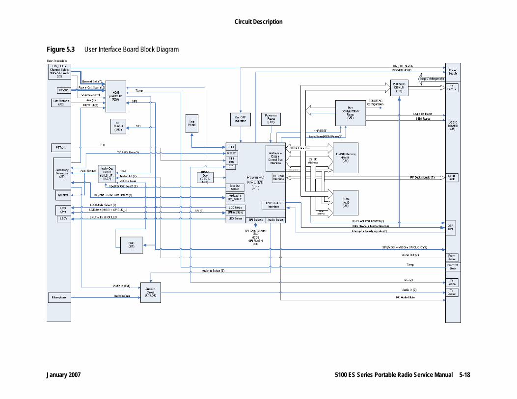
January 2007 5100 ES Series Portable Radio Service Manual 5-18
Circuit Description
Figure 5.3 User Interface Board Block Diagram
January 2007 5100 ES Series Portable Radio Service Manual 5-19
Circuit Description
5.5 Logic BoardThis section provides a functional description of the 5100 ES Portable Radio Logic Board (P/N 023-5500-180/185).
Related Documents• Schematic, 5100 ES Logic Board, P/N 025-5500-180/185• Schematic, 5100 ES UI Board, P/N 025-5500-480/485• MPC885 PowerQUIC Family Reference Manual, Freescale Document
MPC885RM.PDF• Firmware, CPL:D, 5100 ES Logic, P/N 049-0087-200• TMS320VC5510 Fixed-Point Digital Signal Processor, TI Document
TMS320VC5510.PDF• TLV320AIC21 Data Manual, TI Document TLV320AIC21.PDF
Functional DescriptionA functional description of the Logic Board is provided in the following paragraphs. A block diagram of the Logic Board is shown in Figure 5.4.
5.5.1 Power Supplies
The power supply section of the Logic board receives power from the battery and converts it through linear and switching regulators into various other voltages that are used to power the digital and analog circuitry on both the Logic Board and on the UI Board.
Transistors Q1 and Q3 control are used to switch on the battery supply to the Logic Board regulators. These transistors are turned on or off by the radio on/off switch or the power hold signal from the MPC870 processor on the UI Board.

5-20 5100 ES Series Portable Radio Service Manual January 2007
Circuit Description
5.5.1.1 DigitalFour regulators provide power to the digital electronics on the UI and Logic boards. These voltages are as follows:
• 5Vdc (U11) – power for keypad backlights, LCD backlights, and transmit/receive LED• 1.6Vdc(U49) – Logic Board DSP and SEM processor core voltage supply• 1.8Vdc(U46) – Logic Board Codec and CPLD core voltage supply/UI board MPC870
and CPLD core voltage• 3.3Vdc(U47) – Supply for digital I/O and discrete logic devicesThe supplies are powered up in the following sequence, 1.6Vdc, 1.8Vdc, 3.3Vdc, then 5Vdc. This power up sequence is dictated by power application requirements of the DSP and MPC 870 processors. Additionally, the switching regulators (U49, U46, and U47) are synchronized to a 768Khz clock from the CPLD (U20) that is derived from the 12.288 TCXO (Y2).
5.5.1.2 AnalogTwo linear regulators (U11, U45) provide power to the analog circuitry (op amps, Codec) on the Logic and UI boards. The 5Vdc analog supply (U11) powers the audio out section (U9, U10) and Codec 3.3Vdc linear regulator (U45) on the Logic Board. Additionally, the 5Vdc supply provides power to the microphone and audio output circuitry on the UI Board.
5.5.1.3 RF DeckTwo linear regulators supply 3.3Vdc and 5.5Vdc voltages to the RF Deck. The 3.3Vdc supply (U43) powers the digital circuitry on the RF Deck. The 5.5Vdc supplies power to the 5Vdc LDOs used on the RF Deck.
5.5.2 DSP
The Digital Signal Processing (DSP) functions are performed by a TI 5510 DSP (U15) and the TI AIC21 Codec (U27) with the support of MPC870 processor on the UI board. Operation of the DSP is described in the paragraphs below.

January 2007 5100 ES Series Portable Radio Service Manual 5-21
Circuit Description
5.5.2.1 Control InterfaceThe MPC870 processor on the UI Board communicates with the DSP via a multiplexed 16 bit host peripheral (HPI) bus. This interface is used by the MPC870 to load application code into the DSP’s internal SRAM and for exchanging control/status with the DSP. The DSP has three internal registers, accessible by the MPC870, for transferring of data. Access to the internal registers is controlled by the DSP’s chip select (signal H_nCS), data strobe (DSP_DS0), read/write (H_R/nW), and register select (HDS1, HDS2) input signals. The DSP uses its HRDY line to signal the MPC870 when a bus transfer has completed.
5.5.2.2 Transmit OperationIn transmit mode the microphone audio signal is converted to a differential signal on the UI board and then routed to the Codec on the Logic Board where it is digitized by an internal A/D converter and forwarded to the DSP via a synchronous serial interface (SSI) bus. The DSP processes the incoming data and sends the digitized modulation signals for the RF Deck VCO and TCXO back to the Codec via the SSI bus. The Codec converts the digitized modulation signals into analog signals which are level shifted by an op amp (U26) to derive the TXMOD1 and TXMOD2 signals for the RF Deck.
5.5.2.3 Receive OperationIn receive mode, the DSP receives I/Q data from the Rx Backend IC on the RF Deck (J1) via an SSI bus. The Rx Backend IC controls the timing on SSI bus with the clock set to 1.4 MHz and a frame time of 40 KHz. The SSI bus signals from the RF Deck are heavily filtered and are buffered through U20 to improve the wave shape. The DSP filters and demodulates the I/Q samples from the Rx Backend IC. The resulting demodulated signal is sent to the Codec via the SSI bus. The Codec converts the processed signal from the DSP to an audio signal which is passed to an op amp (U8) that converts it to a differential form. This differential signal is amplified on the UI Board and applied to either the internal on external speaker. Additionally, the DSP sends data to the Codec via the SSI bus to adjust the TXMOD1 and TXMOD2 signals to set the RF Deck receiver frequency.

5-22 5100 ES Series Portable Radio Service Manual January 2007
Circuit Description
5.5.3 HPI Bus Multiplexer
The DSP communicates with the MPC870 processor on the UI Board via its 16 bit host peripheral (HPI) bus. This interface is used by the MPC870 to load application code into the DSP internal SRAM and for exchanging control/status with the DSP.
Due to pin limitations on the 60 connector (J2) between the UI and Logic board, the HPI bus is multiplexed across J2 in two 8 bit transfers. The bus transfer is controlled by logic in the CPLD at U20. The signals controlling the transfer (HDS1, HDS2, H_nCS, and H_R/nW – J2 pins 39, 50, 12 and 13) are generated by the MPC870. Operation of the multiplexer logic is shown in the table below.
5.5.4 Codec
The Codec (U27) is a support chip for the DSP. It provides the A/D and D/A conversion between the DSP and the microphone and speaker audio signals and between the DSP and the RF Deck modulation signals.
The operation of the Codec is determined by fourteen internal registers. These registers are configured by the MPC870 on the UI Board via the Codec I2C bus interface. The Codec internal timing is derived from a 12.288 Mhz TCXO (Y2).
The interface to the DSP (U15) is via an SSI bus. The Codec generates the framing and clock signals for this bus as configured by the MPC870 via the I2C control bus. The SSI bus clock (signal CODEC_CLK) is set to 768 KHz with a frame time (signal CODEC_FS) of 24 KHz.
H_nCS H_R/nW HDS1 HDS2 8 bit bus J21 x x x Hi Z0 1 0 1 DSP lsb0 1 1 0 DSP msb0 0 0 1 PPC lsb0 0 1 0 PPC msb

January 2007 5100 ES Series Portable Radio Service Manual 5-23
Circuit Description
5.5.5 SEM Module
The SEM module (U22) consists of a TI 5416 DSP and serial EEPROM device mounted on a 1.0” x 0.6” printed circuit board that in turn is mounted on the Logic Board. The application code resides in the EEPROM and is downloaded into the 5416 DSP after reset.
Operation of the SEM is controlled by the MPC870 on the UI Board through a SPI bus interface on the 5416 DSP. Data to be encrypted or decrypted is passed to the SEM through an SSI bus that is connected to the Logic Board 5510 DSP.

January 2007 5100 ES Series Portable Radio Service Manual 5-24
Circuit Description
Figure 5.4 Logic Board Block Diagram

January 2007 5100 ES Series Portable Radio Service Manual 6-1
S E C T I O N
Chapter 6Alignment Procedure
6.1 PC TunePC Tune software is used to perform alignment procedures on the EFJohnson 5100 series portable radios.
Perform alignment procedures if repairs or adjustments are made that can affect the factory alignment. All adjustments are set digitally using the computer. It is not necessary to disassemble the transceiver to access adjustment points. In addition, audio test signals are generated internally, so an audio generator is not required.
To verify radio operation, perform the Digital Performance Tests and the Analog Performance Tests in the PC Tune manual included on the PC Tune CD.
Figure 6.1 Alignment Setup
5100 Test CableDB9 - Connect To
Serial PortPart No. 023-5100-940
Audio In/Out CablePart No. 023-5100-950
To Communications Analyzer
Communications Analyzer

6-2 5100 ES Series Portable Radio Service Manual January 2007
Alignment Procedure

January 2007 5100 ES Series Portable Radio Service Manual 7-1
S E C T I O N
Chapter 7Troubleshooting
7.1 Start Up Failure LED Indications
Note There are no user-serviceable components in the transceiver.
Table 7.1 Start Up Failure LED Indications
Orange LED Blinks Start Up Failure Start Up Failure Type
1 Incorrect Software The software was loaded on the wrong platform. This indication is displayed if the boot loader version does not match the expected boot loader version number.
2 Bad File Format The parameter file version number does not match the software version in the radio.
3 Parms Fail The backup copy of the parameters (stored in the SPI flash device) is invalid. To remove this error, use PC Configure to write the parameter file.
4 Bad BandThe radio band in the parameter file does not match the radio band in the tuning parameters. This error message displays if a parameter file for the wrong band is downloaded to the radio.
5 Corrupt Parms This error message appears if the parameters checksum is OK, but the parameters file has an error in it. This message does not normally appear.
6 EE PROM Fail The self test timed out and the parameter file has not yet been read and verified.7 DSP Failed The PowerPC never received a power up message from the DSP.
8 Cycle Power This error message appears when there is a communication failure between the DSP and the back end ADC on the RF deck.

7-2 5100 ES Series Portable Radio Service Manual January 2007
Troubleshooting
7.2 User Troubleshooting• When approaching the limits of radio range, the other party may not be able to hear your
transmissions and there may be an increase in background noise when messages are received.
• You may still be out of range even though you can hear a message.
The reason for this is that the signal you are receiving is usually transmitted at a higher power level than the one transmitted by your transceiver.
• Communication may be improved by moving to higher ground or away from shielding objects such as tall buildings or hills.
• If some other problem is occurring, turn power off and then on again to reset the control logic. Also make sure that the controls are properly set.
• If the radio still does not operate correctly, return it for service.
7.3 Low Battery Indicators• A Low Battery Beep sounds once a minute in the standby and transmit modes.• The LED indicator flashes in the receive mode.
7.3.1 Battery Replacement
The battery should be recharged or replaced as soon as possible after the low battery indications appear.
Note If the transceiver contains encryption (hardware) keys, be sure to reattach a battery within approximately one minute to prevent the loss of these keys.

January 2007 5100 ES Series Portable Radio Service Manual 7-3
Troubleshooting
7.4 Additional InformationThe following documentation provides additional information about the 5100 ES Portable Radios.
Tone GuideEach radio comes with a tone reference guide. This guide provides information about the tones used in the 5100 ES Portable Radio.
Quick Reference GuideEach radio comes with a quick reference guide. This guide includes descriptions and graphics of the 5100 ES Portable Radio hardware features.
Operator’s ManualPlease refer to the 5100 ES Model I Operating Manual or the 5100 ES Models II/III Operating Manual for technical information.
7.5 Contact InformationContact EFJohnson at the numbers and e-mail address shown in Section 8.2.

7-4 5100 ES Series Portable Radio Service Manual January 2007
Troubleshooting

January 2007 5100 ES Series Portable Radio Service Manual 8-1
S E C T I O N
Chapter 8Service Information
This section describes how to obtain authorized service for the EFJohnson 5100 ES Portable Radio.
8.1 Product WarrantyThe warranty statement for this equipment is available from your product supplier or from
Warranty DepartmentEFJohnson 1440 Corporate DriveIrving, TX 75038-2401
This information may also be requested from the Warranty Department by phone at the numbers listed in Section 8.2. The Warranty Department may also be contacted for warranty service reports, claim forms, or any other questions concerning warranties or warranty service.
8-2 5100 ES Series Portable Radio Service Manual January 2007
Service Information
8.2 Factory Customer ServiceThe EFJohnson Customer Service Department provides customer assistance on technical problems and the availability of local and factory repair facilities. Regular customer service hours are 8:00 a.m. - 5:00 p.m. Central Time, Monday- Friday. A technical support subscription service is available or support can be purchased on an as-needed basis. The Customer Service Department can be reached using the following telephone numbers:
Toll-Free:(800) 328-3911 (all except Multi-Net)(800) 295-1773 (Multi-Net only)
Fax: (972) 819-0639E-Mail: [email protected]
You can also e-mail a person directly if you know the first initial/last name. For example, if John Smith is an EFJohnson employee, his e-mail address is probably [email protected]
Note Emergency 24-hour technical support is also available at the preceding numbers during off hours, holidays, and weekends.
When your call is answered at EFJohnson, you will hear a brief message informing you of numbers that can be entered to reach various departments. This number may be entered during or after the message using a tone-type telephone. If you have a pulse-type telephone, wait until the message is finished and an operator will come on the line to assist you. When you enter some numbers, another number is requested to further categorize the type of information you need.
You may also contact the Customer Service Department by mail. Please include all information that may be helpful in solving your problem. The mailing address is as follows:
Customer Service DepartmentEFJohnson 1440 Corporate DriveIrving, TX 75038-2401
8.3 Returns for RepairsBefore returning equipment for repair, contact the EFJohnson Customer Service Department as described in the preceding section. They may be able to suggest a solution to the problem, making return of the equipment unnecessary.
Repair service is normally available through local authorized EFJohnson land mobile radio service centers. If local service is not available, the equipment can be returned to the EFJohnson repair depot for repair. However, before returning equipment, contact the Customer Service Department Repair Depot for the correct “Ship To” address.

January 2007 5100 ES Series Portable Radio Service Manual 8-3
Service Information
Be sure to fill out a Factory Repair Request Form #271 for each unit to be repaired, whether it is in or out of warranty. You can obtain it in any of three ways:
• Download it from the EFJohnson Web site’s “Service & Support” section.• Call the EFJohnson Customer Service Department and request it. See Section 8.2.• Request it when you send a unit in for repair.Clearly describe the difficulty experienced in the space provided and also note any prior physical damage to the equipment. Include this form in the shipping container with each unit. Your telephone number and contact name are important as there are times when the technicians may have specific questions that need to be answered to completely identify and repair a problem.
When returning equipment for repair, it is also recommended that you use a PO number or some other reference number on your paperwork in case you need to call the repair lab about your unit. These numbers are referenced on the repair order and make it easier and faster to locate your unit in the lab.
Return Authorization (RA) numbers are not necessary unless you have been given one by the Field Service Department. RA numbers are required for exchange units or if the Field Service Department wants to be aware of a specific problem. If you have been given an RA number, reference this number on the Factory Repair Request Form sent with the unit. The repair lab will then contact the Field Service Department when the unit arrives. For additional information on factory service, the Depot Service Department can be contacted at the following e-mail address:
8.4 Replacement PartsReplacement parts can be ordered directly from the Service Parts Department. To order parts by phone, dial the toll-free number as described in Section 8.2. When ordering, please supply the part number and quantity of each part ordered. The accessories available for this transceiver are shown in the accessories listing in Table 1.1.
EFJohnson dealers also need to give their account number. If there is uncertainty about the part number, include the designator (C512, for example) and the model number of the equipment the part is from.
You may also send your order by mail or fax. The mailing address is as follows and the fax number is shown in Section 8.2.
Service Parts DepartmentEFJohnson 1440 Corporate DriveIrving, TX 75038-2401

8-4 5100 ES Series Portable Radio Service Manual January 2007
Service Information
8.5 Internet Home PageEFJohnson has a site on the World Wide Web that can be accessed for information on the company about such things as products, systems, and regulations. The address is
http://www.efjohnson.com
January 2007 5100 ES Series Portable Radio Service Manual 9-1
S E C T I O N
Chapter 9Parts List
9.1 PartsThis section lists the 5100 ES Model I/II/III Portable Radio component descriptions, reference designators (Ref No.), and part numbers (Part No.).

9-2 5100 ES Series Portable Radio Service Manual January 2007
Parts List Model I 7/800 MHz, No SEM, Black, No Display
Ref Number Description Part NumberModel I 7/800 MHz, No SEM, Black, No Display 023-5170-161
A 050 ASSEMBLY, FR HOUSING, W/O UI PCB, PLAIN, BLACK(See separate listing on Page 9-2.)
023-5100-341
A 080 COMMON PARTS, FINAL ASSEMBLY(See separate listing on Page 9-3.)
023-5100-085
A 100 5100G LOGIC BD, NON-ENCRYPTED(See separate listing on Page 9-4.)
023-5500-185
A 200 RF MODULE 700/800 MHz CALAMP 6A830 585-5500-710A 400 ASSEMBLY, UI PCB, PLAIN
(See separate listing on Page 9-9.)023-5100-485
Ref Number Description Part NumberAssembly, Front Housing, Without UI PCB, Plain, Black 023-5100-341
A 040 ASSEMBLY CONTROLS, 5100(See separate listing on Page 9-2.)
023-5100-045
A 060 ASSEMBLY, FRONT HOUSING, BLACK, PLAIN 587-5100-06104
HW 102 SPNR NUT M6-.75-6H MET 013-1313-005HW 105 SPNR NUT M6-.75-6H MET 013-1313-005
MP 006 LIGHTPIPE / SLEEVE ASSEMBLY 032-0431-194MP 104 BUTTON, EMERGENCY 320-4312-0801MP 105 5100 3 POS SELECTOR RING 015-0805-653MP 106 SPACER, SELECTOR SWITCH 5100 032-0431-166MP 107 KNOB, SELECTOR, 5100 032-5100-100MP 108 KNOB, VOLUME, 5100 032-5100-101MP 110 KEYPAD, PLAIN 320-4312-0103MP 111 BEZEL, FRONT, NON-DTMF, BLACK 320-4311-4504
NP 101 LABEL, EFJ LOGO, FRONT 5100 559-5000-550
Ref Number Description Part NumberAssembly Controls 023-5100-045
EP 101 TOP SWITCH SEAL 574-3500-071EP 102 TOP SWITCH SEAL 574-3500-071
MP 040 SWITCH HOLDER NGP 5100 032-0431-171
PC 040 FLEX CKT, CONTROLS (REV 1) 355-1000-4501

January 2007 5100 ES Series Portable Radio Service Manual 9-3
Parts ListCommon Parts, Final Assembly
R 101 HIGH TORQUE WIPING ON / OFF SWITCH 562-0018-067
S 101 HIGH DETENT SELECT SWITCH 5100 583-2009-047
Ref Number Description Part NumberCommon Parts, Final Assembly 023-5100-085
A 030 REAR HOUSING ASSEMBLY 5100 GREEN(See separate listing on Page 9-3.)
023-5100-035
A 035 BATTERY CONTACT ASSEMBLY 5100 585-5100-017A 070 ASSEMBLY, REAR HOUSING SHIELD 587-5100-07101
EP 120 THIN WALL TEFLON TUBE - (3/16 LENGTH) 574-5100-120
HW 031 MOLDED SILICON, NI/C, BLACK, ORING .301 X .070 574-2510-001HW 103 SCREW, THREAD FORMING, M1.8 X 6 575-7800-10001
MK 101 MIC CARTRIDGE 589-0301-003
ML 000 36 YD x 1/4 ROLL POLYMIDE TAPE 042-0241-241ML 003 .020 62/36/2RA44CORE58 042-0211-234
MP 113 BRACKET, SPEAKER 172-2295-6201MP 120 CLIP, SHIELD, REAR HOUSING 172-2295-8101MP 201 CONDUCTIVE COMPRESSION SPACER 574-5100-005
NP 002 WINDRIVER VXWORKS LICENSE LABEL 5100/5300 559-5000-558
SP 101 SPEAKER, 45mm, 16 OHM, W/GASKET 589-1015-00901
Ref Number Description Part NumberRear Housing Assembly 023-5100-035
CH 030 HOUSING, REAR 150-8056-5401
J 030 PRESS FIT SMA CONNECTOR 5100 PORTABLE ASSY **AIR** 051-5900-6130
ML 000 LOCTITE 290 THREAD LOCKER WICKING TYPE GREEN 042-0181-591
Ref Number Description Part Number

9-4 5100 ES Series Portable Radio Service Manual January 2007
Parts List Logic Board, Non-Encrypted
Ref Number Description Part NumberLogic Board, Non-Encrypted 023-5500-185
C 001 CAP, 10 µF, 10%, 402, 25V 510-3681-100C 002 CAP, 10 µF, 10%, 402, 25V 510-3681-100C 003 CAP, 33 µF, 10%, 402, 25V 510-3681-330C 004 CAP, 0.01 µF, 0402, 10%TOL 510-3681-103C 014 CAP, 0.01 µF, 0402, 10%TOL 510-3681-103C 015 CAP, 0.01 µF, 0402, 10%TOL 510-3681-103C 016 CAP, 0.01 µF, 0402, 10%TOL 510-3681-103C 017 CAP, 0.1 µF, 16V, 10%, X7R, 0402 510-3687-104C 018 CAP, 0.01 µF, 0402, 10%TOL 510-3681-103C 019 CAP, 0.01 µF, 0402, 10%TOL 510-3681-103C 020 CAP, 0.01 µF, 0402, 10%TOL 510-3681-103C 021 CAP, 0.1 µF, 16V, 10%, X7R, 0402 510-3687-104C 022 CAP, 0.1 µF, 16V, 10%, X7R, 0402 510-3687-104C 023 CAP, 0.1 µF, 16V, 10%, X7R, 0402 510-3687-104C 024 CAP, 0.01 µF, 0402, 10%TOL 510-3681-103C 025 CAP, 0.01 µF, 0402, 10%TOL 510-3681-103C 026 CAP, 0.1 µF, 16V, 10%, X7R, 0402 510-3687-104C 027 CAP, 0.1 µF, 16V, 10%, X7R, 0402 510-3687-104C 059 CAP, 0.1 µF, 16V, 10%, X7R, 0402 510-3687-104C 063 CAP, 0.1 µF, 16V, 10%, X7R, 0402 510-3687-104C 064 CAP, 0.01 µF, 0402, 10%TOL 510-3681-103C 065 4.7 µF 10V SMD TANT RL 510-2624-479C 066 CERAMIC CAPACITOR, 10 µF, 1206, 10V 510-3755-106C 067 CAP, 22 µF, 10%, 16V, X5R, 1210 510-3607-226C 070 CERAMIC CAPACITOR, 1.0 µF, 0805, 16V 510-3923-105C 076 4.7 µF 10V SMD TANT RL 510-2624-479C 077 CERAMIC CAPACITOR, 10 µF, 1206, 10V 510-3755-106C 078 4.7 µF 10V SMD TANT RL 510-2624-479C 079 CAP, 33 µF, 10%, 402, 25V 510-3681-330C 080 CAP, 33 µF, 10%, 402, 25V 510-3681-330C 081 CAP, 33 µF, 10%, 402, 25V 510-3681-330C 082 CAP, 33 µF, 10%, 402, 25V 510-3681-330C 084 CAP, 33 µF, 10%, 402, 25V 510-3681-330C 085 CAP, 33 µF, 10%, 402, 25V 510-3681-330C 087 CAP, 33 µF, 10%, 402, 25V 510-3681-330C 090 CAP, 0.01 µF, 0402, 10%TOL 510-3681-103C 091 CAP, 22 µF, 10%, 16V, X5R, 1210 510-3607-226C 092 CAP, 0.01 µF, 0402, 10%TOL 510-3681-103C 100 CAP, 0.1 µF, 16V, 10%, X7R, 0402 510-3687-104C 101 CAP, 0.01 µF, 0402, 10%TOL 510-3681-103

January 2007 5100 ES Series Portable Radio Service Manual 9-5
Parts ListLogic Board, Non-Encrypted
C 102 4.7 µF 10V SMD TANT RL 510-2624-479C 104 CAP, 0.1 µF, 16V, 10%, X7R, 0402 510-3687-104C 105 CAP, 0.1 µF, 16V, 10%, X7R, 0402 510-3687-104C 109 CAP, 22 µF, 10%, 16V, X5R, 1210 510-3607-226C 110 CAP, 0.01 µF, 0402, 10%TOL 510-3681-103C 111 CAP, 0.01 µF, 0402, 10%TOL 510-3681-103C 114 CAP, 10 µF, 10%, 402, 25V 510-3681-100C 115 CAP, 10 µF, 10%, 402, 25V 510-3681-100C 117 CAP, 0.1 µF, 16V, 10%, X7R, 0402 510-3687-104C 118 CAP, 0.1 µF, 16V, 10%, X7R, 0402 510-3687-104C 119 CAP, 0.01 µF, 0402, 10%TOL 510-3681-103C 120 CAP, 0.01 µF, 0402, 10%TOL 510-3681-103C 121 CAP, 0.1 µF, 16V, 10%, X7R, 0402 510-3687-104C 122 CAP, 0.1 µF, 16V, 10%, X7R, 0402 510-3687-104C 123 CERAMIC CAPACITOR, 10 µF, 1206, 10V 510-3755-106C 124 CAP, 0.1 µF, 16V, 10%, X7R, 0402 510-3687-104C 125 CAP, 0.1 µF, 16V, 10%, X7R, 0402 510-3687-104C 126 CAP, 0.1 µF, 16V, 10%, X7R, 0402 510-3687-104C 127 CAP, 0.1 µF, 16V, 10%, X7R, 0402 510-3687-104C 128 CAP, 0.1 µF, 16V, 10%, X7R, 0402 510-3687-104C 129 CAP, 0.1 µF, 16V, 10%, X7R, 0402 510-3687-104C 130 CAP, 0.1 µF, 16V, 10%, X7R, 0402 510-3687-104C 132 CAP, 0.01 µF, 0402, 10%TOL 510-3681-103C 133 CAP, 0.01 µF, 0402, 10%TOL 510-3681-103C 134 CAP, 0.1 µF, 16V, 10%, X7R, 0402 510-3687-104C 135 10 µF, 16V, 10% TANTALUM CAPACITOR LOW-ESR,T494 510-2642-100C 137 CAP, 0.1 µF, 16V, 10%, X7R, 0402 510-3687-104C 138 CAP, 0.01 µF, 0402, 10%TOL 510-3681-103C 139 CERAMIC CAPACITOR, 1.0 µF, 0805, 16V 510-3923-105C 140 CERAMIC CAPACITOR, 1.0 µF, 0805, 16V 510-3923-105C 141 CERAMIC CAPACITOR, 1.0 µF, 0805, 16V 510-3923-105C 142 CAP, 0.01 µF, 0402, 10%TOL 510-3681-103C 143 CAP, 0.01 µF, 0402, 10%TOL 510-3681-103C 144 CAP, 0.1 µF, 16V, 10%, X7R, 0402 510-3687-104C 145 CAP, 0.1 µF, 16V, 10%, X7R, 0402 510-3687-104C 146 CAP, 0.1 µF, 16V, 10%, X7R, 0402 510-3687-104C 147 CAP, 0.1 µF, 16V, 10%, X7R, 0402 510-3687-104C 148 CAP, 0.1 µF, 16V, 10%, X7R, 0402 510-3687-104C 149 CAP, 0.01 µF, 0402, 10%TOL 510-3681-103C 150 CAP, 0.01 µF, 0402, 10%TOL 510-3681-103C 151 CAP, 470 µF, 10%, 402, 25V 510-3681-471C 152 CAP, 0.1 µF, 16V, 10%, X7R, 0402 510-3687-104C 153 CAP, 0.01 µF, 0402, 10%TOL 510-3681-103
Ref Number Description Part Number

9-6 5100 ES Series Portable Radio Service Manual January 2007
Parts List Logic Board, Non-Encrypted
C 154 CAP, 0.01 µF, 0402, 10%TOL 510-3681-103C 155 CAP, 0.01 µF, 0402, 10%TOL 510-3681-103C 157 CAP, 0.01 µF, 0402, 10%TOL 510-3681-103C 158 CAP, 0.01 µF, 0402, 10%TOL 510-3681-103C 159 CAP, 0.01 µF, 0402, 10%TOL 510-3681-103
CR 001 DUAL DIODES-COM ANODES 523-1504-024CR 008 DUAL DIODES-COM ANODES 523-1504-024
J 001 CONN, 26-P, ZIF 0.5MM PITCH SMD 515-7111-526J 002 FINE PITCH SMD BD TO BD RECEP 60 PIN(TR) 515-7111-650J 003 SINGLE SPRING CLIP BRIGHT TINNED 75RC-.05-08 537-5001-014J 004 SINGLE SPRING CLIP BRIGHT TINNED 75RC-.05-08 537-5001-014
L 003 10 µH SMT POWER INDUCTOR (SD12-100) 542-9009-100L 004 10 µH SMT POWER INDUCTOR (SD12-100) 542-9009-100L 005 270 nH 0603 SMD INDUCTOR 542-9017-274L 007 270 nH 0603 SMD INDUCTOR 542-9017-274L 010 270 nH 0603 SMD INDUCTOR 542-9017-274L 011 INDUCTOR, 27 µH, 1.2A, SMD 542-5010-019L 013 270 nH 0603 SMD INDUCTOR 542-9017-274L 014 270 nH 0603 SMD INDUCTOR 542-9017-274L 015 270 nH 0603 SMD INDUCTOR 542-9017-274L 016 10 µH SMT POWER INDUCTOR (SD12-100) 542-9009-100
PC 001 PCB, 5100G LOGIC BOARD 035-5500-180
Q 001 POWER MOSFET N+P PAIR 20 V SC-70 576-0006-244Q 002 GEN PURPOSE 3904 BST SC-75 576-0001-029Q 003 POWER MOSFET N+P PAIR 20 V SC-70 576-0006-244
R 002 RES, 10K, 5%, 402 569-0165-103R 003 RES, 10K, 5%, 402 569-0165-103R 004 RES, 100K, 0.06W, 5%, 402 569-0165-104R 005 RES, 100K, 0.06W, 5%, 402 569-0165-104R 009 RES, 0 ohm, 5%, 402 569-0165-001R 019 RESISTOR, 1K OHM, 0402, SMT 569-0165-102R 020 RESISTOR, 15K OHM, 0402, SMT 569-0165-153R 022 SURFACE MOUNT 20K, 0402, RESISTOR 569-0165-203R 023 RESISTOR, 15K OHM, 0402, SMT 569-0165-153R 024 RESISTOR, 1K OHM, 0402, SMT 569-0165-102R 028 RES, 4.7K, 5%, 402 569-0165-472R 029 RES, 4.7K, 5%, 402 569-0165-472
Ref Number Description Part Number

January 2007 5100 ES Series Portable Radio Service Manual 9-7
Parts ListLogic Board, Non-Encrypted
R 030 RES, 10K, 5%, 402 569-0165-103R 031 RES, 30.1K, 1%, 0402 569-0161-447R 032 RES, 30.1K, 1%, 0402 569-0161-447R 033 SURFACE MOUNT 20K, 0402, RESISTOR 569-0165-203R 059 RESISTOR 1%, 0402, 100K OHM 569-0161-501R 060 RESISTOR 1%, 0402, 100K OHM 569-0161-501R 061 RESISTOR 1%, 0402, 100K OHM 569-0161-501R 062 RESISTOR 1%, 0402, 100K OHM 569-0161-501R 063 RESISTOR 1%, 0402, 100K OHM 569-0161-501R 064 RES, 100K, 0.06W, 5%, 402 569-0165-104R 065 RES, 100K, 0.06W, 5%, 402 569-0165-104R 068 RES, 100K, 0.06W, 5%, 402 569-0165-104R 069 RES, 100K, 0.06W, 5%, 402 569-0165-104R 078 RESISTOR 1%, 221K, 0402 569-0161-534R 081 RESISTOR 1%, 0603, 100K OHM 569-0151-501R 088 RESISTOR, 1K OHM, 0402, SMT 569-0165-102R 090 RESISTOR, 1K OHM, 0402, SMT 569-0165-102R 091 RES, 10K, 5%, 402 569-0165-103R 092 RES, 10K, 5%, 402 569-0165-103R 097 RES, 10K, 5%, 402 569-0165-103R 098 RES, 10K, 5%, 402 569-0165-103R 100 RESISTOR, 1K OHM, 0402, SMT 569-0165-102R 101 RESISTOR, 1K OHM, 0402, SMT 569-0165-102R 102 RESISTOR, 1K OHM, 0402, SMT 569-0165-102R 103 RESISTOR 1%, 0603, 13K OHM 569-0151-412R 105 RESISTOR, 1K OHM, 0402, SMT 569-0165-102R 106 RESISTOR, 1K OHM, 0402, SMT 569-0165-102R 107 RESISTOR 1%, 0603, 20K OHM 569-0151-430R 110 RESISTOR 1%, 0603, 38.3K OHM 569-0151-457R 111 RESISTOR 1%, 0603, 12.1K OHM 569-0151-409R 182 RES, 10K, 5%, 402 569-0165-103R 186 RES, 10K, 5%, 402 569-0165-103R 188 RES, 10K, 5%, 402 569-0165-103R 190 RES, 10K, 5%, 402 569-0165-103R 191 RES, 10K, 5%, 402 569-0165-103R 193 RES, 10K, 5%, 402 569-0165-103R 194 RES, 10K, 5%, 402 569-0165-103R 195 RES, 10K, 5%, 402 569-0165-103R 236 RESISTOR, 1K OHM, 0402, SMT 569-0165-102R 237 RESISTOR, 1K OHM, 0402, SMT 569-0165-102R 238 RESISTOR, 1K OHM, 0402, SMT 569-0165-102R 239 RESISTOR, 1K OHM, 0402, SMT 569-0165-102R 240 RESISTOR, 1K OHM, 0402, SMT 569-0165-102
Ref Number Description Part Number
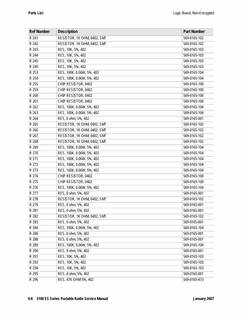
9-8 5100 ES Series Portable Radio Service Manual January 2007
Parts List Logic Board, Non-Encrypted
R 241 RESISTOR, 1K OHM, 0402, SMT 569-0165-102R 242 RESISTOR, 1K OHM, 0402, SMT 569-0165-102R 243 RES, 10K, 5%, 402 569-0165-103R 244 RES, 10K, 5%, 402 569-0165-103R 245 RES, 10K, 5%, 402 569-0165-103R 249 RES, 10K, 5%, 402 569-0165-103R 253 RES, 100K, 0.06W, 5%, 402 569-0165-104R 254 RES, 100K, 0.06W, 5%, 402 569-0165-104R 255 CHIP RESISTOR, 0402 569-0165-100R 259 CHIP RESISTOR, 0402 569-0165-100R 260 CHIP RESISTOR, 0402 569-0165-100R 261 CHIP RESISTOR, 0402 569-0165-100R 262 RES, 100K, 0.06W, 5%, 402 569-0165-104R 263 RES, 100K, 0.06W, 5%, 402 569-0165-104R 264 RES, 0 ohm, 5%, 402 569-0165-001R 265 RESISTOR, 1K OHM, 0402, SMT 569-0165-102R 266 RESISTOR, 1K OHM, 0402, SMT 569-0165-102R 267 RESISTOR, 1K OHM, 0402, SMT 569-0165-102R 268 RESISTOR, 1K OHM, 0402, SMT 569-0165-102R 269 RES, 100K, 0.06W, 5%, 402 569-0165-104R 270 RES, 100K, 0.06W, 5%, 402 569-0165-104R 271 RES, 100K, 0.06W, 5%, 402 569-0165-104R 272 RES, 100K, 0.06W, 5%, 402 569-0165-104R 273 RES, 100K, 0.06W, 5%, 402 569-0165-104R 274 CHIP RESISTOR, 0402 569-0165-100R 275 CHIP RESISTOR, 0402 569-0165-100R 276 RES, 100K, 0.06W, 5%, 402 569-0165-104R 277 RES, 0 ohm, 5%, 402 569-0165-001R 278 RESISTOR, 1K OHM, 0402, SMT 569-0165-102R 279 RES, 0 ohm, 5%, 402 569-0165-001R 281 RES, 0 ohm, 5%, 402 569-0165-001R 282 RESISTOR, 1K OHM, 0402, SMT 569-0165-102R 283 RES, 0 ohm, 5%, 402 569-0165-001R 284 RES, 100K, 0.06W, 5%, 402 569-0165-104R 286 RES, 0 ohm, 5%, 402 569-0165-001R 288 RES, 0 ohm, 5%, 402 569-0165-001R 289 RES, 100K, 0.06W, 5%, 402 569-0165-104R 290 RES, 0 ohm, 5%, 402 569-0165-001R 291 RES, 10K, 5%, 402 569-0165-103R 292 RES, 10K, 5%, 402 569-0165-103R 294 RES, 10K, 5%, 402 569-0165-103R 295 RES, 0 ohm, 5%, 402 569-0165-001R 296 RES, 47K OHM 5%, 402 569-0165-473
Ref Number Description Part Number

January 2007 5100 ES Series Portable Radio Service Manual 9-9
Parts ListAssembly, UI PC Board, Plain
R 297 RES, 47K OHM 5%, 402 569-0165-473R 299 RES, 0 ohm, 5%, 402 569-0165-001R 301 CHIP RESISTOR, 0402 569-0165-100R 302 CHIP RESISTOR, 0402 569-0165-100R 303 CHIP RESISTOR, 0402 569-0165-100R 306 CHIP RESISTOR, 0402 569-0165-100
U 008 OPAMP, QUAD SINGLE SPLY SSOP 544-2020-013U 009 SINGLE SUPPLY SPDT ANALOG SWITCH SC-70 544-4002-007U 011 LDO, DMOS400MA 5V 8P MSOP 544-2603-055U 015 DSP,TMS3205510AGGWA1, 160MHz BGA trays 544-5003-133U 016 SINGLE SUPPLY SPDT ANALOG SWITCH SC-70 544-4002-007U 017 SINGLE SUPPLY SPDT ANALOG SWITCH SC-70 544-4002-007U 018 LDO, DMOS400MA 5V 8P MSOP 544-2603-055U 020 IC, CPLD, 64 CELL, 45 IO, MIXED IO VOLTAGE 544-5001-421U 026 OpAmp, Dual, single sply 8p 544-2018-015U 027 AIC21 16-BIT DUAL CODEC, LOW POWER 544-3016-057U 042 REGULATOR LDO, ADJ TO 5.5V 500mA, MSOP-8 544-2603-057U 043 REGULATOR LDO, ADJ TO 5.5V 500mA, MSOP-8 544-2603-057U 045 IC, LDO, 3.3V, 150MA, SOT23, TPS73133 544-2603-068U 046 CONV, SYNC STEP DOWN, 2.7-10V IN. 1.8V OUT 544-4006-012U 047 CONV, SYNC STEP DOWN V.REG, 2.7-10V IN, 3.3V OUT 544-4006-014U 049 CONV, SYNC STEP DOWN, 2.7-10V IN. VAR OUT 544-4006-010Y 002 TCXO, 12.288 MHz, 2PPM, HCMOS 518-7012-210
Ref Number Description Part NumberAssembly, UI PC Board, Plain 023-5100-485
A 001 5100G UI BD, W/O DISPLAY (MODEL 1) Eff end 01-10-07 023-5500-485A 001 5100G UI BD, W/O DISPLAY, NON-FM Eff begin 01-11-07 023-5500-487EP 010 FOAM FRAME DISPLAY BACKLIGHT 5100 574-3500-065MP 005 SPACER, LCD, 5180x 325-1001-2501
Ref Number Description Part NumberUI Board without Display 023-5500-485
C 013 CAP, 100 µF, 402, 25V, 10% 510-3681-101C 014 CAP, 100 µF, 402, 25V, 10% 510-3681-101C 029 CERAMIC CAPACITOR, 10 µF, 1206, 10V 510-3755-106C 030 CAP, 0.1 µF, 16V, 10%, X7R, 0402 510-3687-104C 035 CAP, 0.1 µF, 16V, 10%, X7R, 0402 510-3687-104
Ref Number Description Part Number
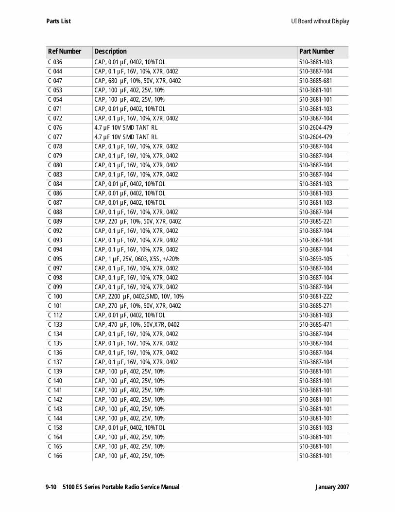
9-10 5100 ES Series Portable Radio Service Manual January 2007
Parts List UI Board without Display
C 036 CAP, 0.01 µF, 0402, 10%TOL 510-3681-103C 044 CAP, 0.1 µF, 16V, 10%, X7R, 0402 510-3687-104C 047 CAP, 680 µF, 10%, 50V, X7R, 0402 510-3685-681C 053 CAP, 100 µF, 402, 25V, 10% 510-3681-101C 054 CAP, 100 µF, 402, 25V, 10% 510-3681-101C 071 CAP, 0.01 µF, 0402, 10%TOL 510-3681-103C 072 CAP, 0.1 µF, 16V, 10%, X7R, 0402 510-3687-104C 076 4.7 µF 10V SMD TANT RL 510-2604-479C 077 4.7 µF 10V SMD TANT RL 510-2604-479C 078 CAP, 0.1 µF, 16V, 10%, X7R, 0402 510-3687-104C 079 CAP, 0.1 µF, 16V, 10%, X7R, 0402 510-3687-104C 080 CAP, 0.1 µF, 16V, 10%, X7R, 0402 510-3687-104C 083 CAP, 0.1 µF, 16V, 10%, X7R, 0402 510-3687-104C 084 CAP, 0.01 µF, 0402, 10%TOL 510-3681-103C 086 CAP, 0.01 µF, 0402, 10%TOL 510-3681-103C 087 CAP, 0.01 µF, 0402, 10%TOL 510-3681-103C 088 CAP, 0.1 µF, 16V, 10%, X7R, 0402 510-3687-104C 089 CAP, 220 µF, 10%, 50V, X7R, 0402 510-3685-221C 092 CAP, 0.1 µF, 16V, 10%, X7R, 0402 510-3687-104C 093 CAP, 0.1 µF, 16V, 10%, X7R, 0402 510-3687-104C 094 CAP, 0.1 µF, 16V, 10%, X7R, 0402 510-3687-104C 095 CAP, 1 µF, 25V, 0603, X5S, +/-20% 510-3693-105C 097 CAP, 0.1 µF, 16V, 10%, X7R, 0402 510-3687-104C 098 CAP, 0.1 µF, 16V, 10%, X7R, 0402 510-3687-104C 099 CAP, 0.1 µF, 16V, 10%, X7R, 0402 510-3687-104C 100 CAP, 2200 µF, 0402,SMD, 10V, 10% 510-3681-222C 101 CAP, 270 µF, 10%, 50V, X7R, 0402 510-3685-271C 112 CAP, 0.01 µF, 0402, 10%TOL 510-3681-103C 133 CAP, 470 µF, 10%, 50V,X7R, 0402 510-3685-471C 134 CAP, 0.1 µF, 16V, 10%, X7R, 0402 510-3687-104C 135 CAP, 0.1 µF, 16V, 10%, X7R, 0402 510-3687-104C 136 CAP, 0.1 µF, 16V, 10%, X7R, 0402 510-3687-104C 137 CAP, 0.1 µF, 16V, 10%, X7R, 0402 510-3687-104C 139 CAP, 100 µF, 402, 25V, 10% 510-3681-101C 140 CAP, 100 µF, 402, 25V, 10% 510-3681-101C 141 CAP, 100 µF, 402, 25V, 10% 510-3681-101C 142 CAP, 100 µF, 402, 25V, 10% 510-3681-101C 143 CAP, 100 µF, 402, 25V, 10% 510-3681-101C 144 CAP, 100 µF, 402, 25V, 10% 510-3681-101C 158 CAP, 0.01 µF, 0402, 10%TOL 510-3681-103C 164 CAP, 100 µF, 402, 25V, 10% 510-3681-101C 165 CAP, 100 µF, 402, 25V, 10% 510-3681-101C 166 CAP, 100 µF, 402, 25V, 10% 510-3681-101
Ref Number Description Part Number
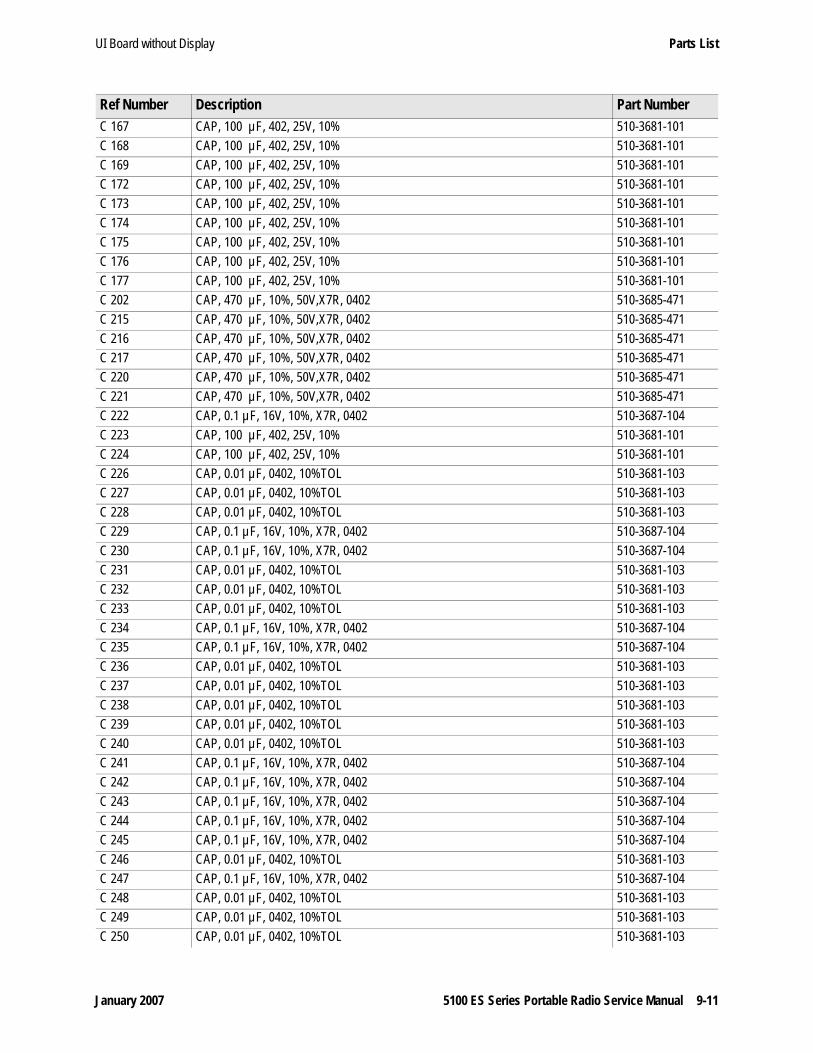
January 2007 5100 ES Series Portable Radio Service Manual 9-11
Parts ListUI Board without Display
C 167 CAP, 100 µF, 402, 25V, 10% 510-3681-101C 168 CAP, 100 µF, 402, 25V, 10% 510-3681-101C 169 CAP, 100 µF, 402, 25V, 10% 510-3681-101C 172 CAP, 100 µF, 402, 25V, 10% 510-3681-101C 173 CAP, 100 µF, 402, 25V, 10% 510-3681-101C 174 CAP, 100 µF, 402, 25V, 10% 510-3681-101C 175 CAP, 100 µF, 402, 25V, 10% 510-3681-101C 176 CAP, 100 µF, 402, 25V, 10% 510-3681-101C 177 CAP, 100 µF, 402, 25V, 10% 510-3681-101C 202 CAP, 470 µF, 10%, 50V,X7R, 0402 510-3685-471C 215 CAP, 470 µF, 10%, 50V,X7R, 0402 510-3685-471C 216 CAP, 470 µF, 10%, 50V,X7R, 0402 510-3685-471C 217 CAP, 470 µF, 10%, 50V,X7R, 0402 510-3685-471C 220 CAP, 470 µF, 10%, 50V,X7R, 0402 510-3685-471C 221 CAP, 470 µF, 10%, 50V,X7R, 0402 510-3685-471C 222 CAP, 0.1 µF, 16V, 10%, X7R, 0402 510-3687-104C 223 CAP, 100 µF, 402, 25V, 10% 510-3681-101C 224 CAP, 100 µF, 402, 25V, 10% 510-3681-101C 226 CAP, 0.01 µF, 0402, 10%TOL 510-3681-103C 227 CAP, 0.01 µF, 0402, 10%TOL 510-3681-103C 228 CAP, 0.01 µF, 0402, 10%TOL 510-3681-103C 229 CAP, 0.1 µF, 16V, 10%, X7R, 0402 510-3687-104C 230 CAP, 0.1 µF, 16V, 10%, X7R, 0402 510-3687-104C 231 CAP, 0.01 µF, 0402, 10%TOL 510-3681-103C 232 CAP, 0.01 µF, 0402, 10%TOL 510-3681-103C 233 CAP, 0.01 µF, 0402, 10%TOL 510-3681-103C 234 CAP, 0.1 µF, 16V, 10%, X7R, 0402 510-3687-104C 235 CAP, 0.1 µF, 16V, 10%, X7R, 0402 510-3687-104C 236 CAP, 0.01 µF, 0402, 10%TOL 510-3681-103C 237 CAP, 0.01 µF, 0402, 10%TOL 510-3681-103C 238 CAP, 0.01 µF, 0402, 10%TOL 510-3681-103C 239 CAP, 0.01 µF, 0402, 10%TOL 510-3681-103C 240 CAP, 0.01 µF, 0402, 10%TOL 510-3681-103C 241 CAP, 0.1 µF, 16V, 10%, X7R, 0402 510-3687-104C 242 CAP, 0.1 µF, 16V, 10%, X7R, 0402 510-3687-104C 243 CAP, 0.1 µF, 16V, 10%, X7R, 0402 510-3687-104C 244 CAP, 0.1 µF, 16V, 10%, X7R, 0402 510-3687-104C 245 CAP, 0.1 µF, 16V, 10%, X7R, 0402 510-3687-104C 246 CAP, 0.01 µF, 0402, 10%TOL 510-3681-103C 247 CAP, 0.1 µF, 16V, 10%, X7R, 0402 510-3687-104C 248 CAP, 0.01 µF, 0402, 10%TOL 510-3681-103C 249 CAP, 0.01 µF, 0402, 10%TOL 510-3681-103C 250 CAP, 0.01 µF, 0402, 10%TOL 510-3681-103
Ref Number Description Part Number
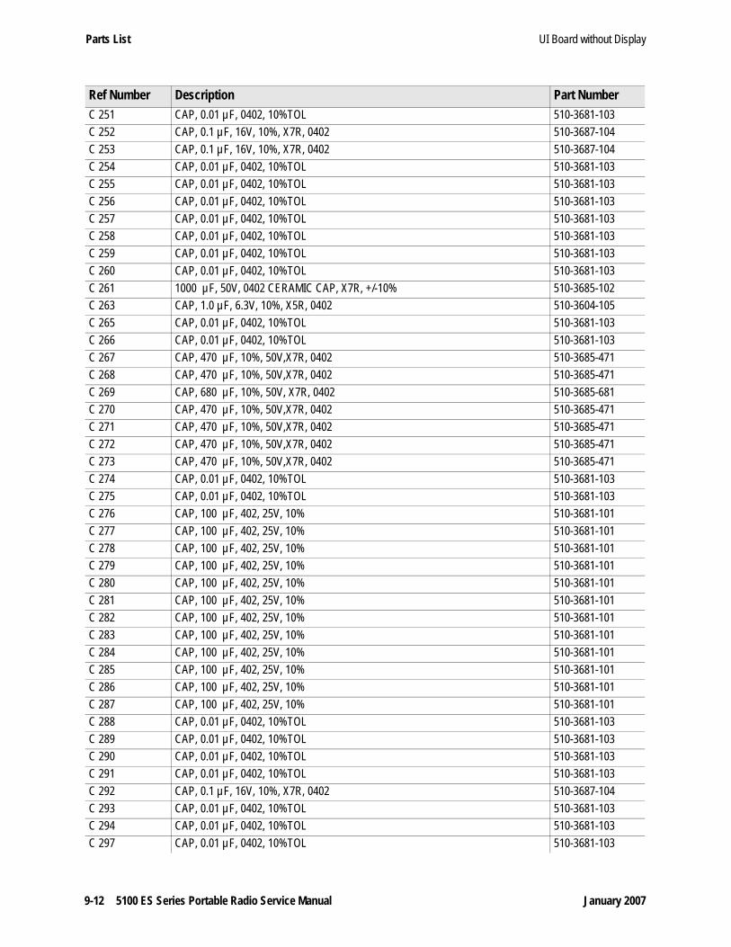
9-12 5100 ES Series Portable Radio Service Manual January 2007
Parts List UI Board without Display
C 251 CAP, 0.01 µF, 0402, 10%TOL 510-3681-103C 252 CAP, 0.1 µF, 16V, 10%, X7R, 0402 510-3687-104C 253 CAP, 0.1 µF, 16V, 10%, X7R, 0402 510-3687-104C 254 CAP, 0.01 µF, 0402, 10%TOL 510-3681-103C 255 CAP, 0.01 µF, 0402, 10%TOL 510-3681-103C 256 CAP, 0.01 µF, 0402, 10%TOL 510-3681-103C 257 CAP, 0.01 µF, 0402, 10%TOL 510-3681-103C 258 CAP, 0.01 µF, 0402, 10%TOL 510-3681-103C 259 CAP, 0.01 µF, 0402, 10%TOL 510-3681-103C 260 CAP, 0.01 µF, 0402, 10%TOL 510-3681-103C 261 1000 µF, 50V, 0402 CERAMIC CAP, X7R, +/-10% 510-3685-102C 263 CAP, 1.0 µF, 6.3V, 10%, X5R, 0402 510-3604-105C 265 CAP, 0.01 µF, 0402, 10%TOL 510-3681-103C 266 CAP, 0.01 µF, 0402, 10%TOL 510-3681-103C 267 CAP, 470 µF, 10%, 50V,X7R, 0402 510-3685-471C 268 CAP, 470 µF, 10%, 50V,X7R, 0402 510-3685-471C 269 CAP, 680 µF, 10%, 50V, X7R, 0402 510-3685-681C 270 CAP, 470 µF, 10%, 50V,X7R, 0402 510-3685-471C 271 CAP, 470 µF, 10%, 50V,X7R, 0402 510-3685-471C 272 CAP, 470 µF, 10%, 50V,X7R, 0402 510-3685-471C 273 CAP, 470 µF, 10%, 50V,X7R, 0402 510-3685-471C 274 CAP, 0.01 µF, 0402, 10%TOL 510-3681-103C 275 CAP, 0.01 µF, 0402, 10%TOL 510-3681-103C 276 CAP, 100 µF, 402, 25V, 10% 510-3681-101C 277 CAP, 100 µF, 402, 25V, 10% 510-3681-101C 278 CAP, 100 µF, 402, 25V, 10% 510-3681-101C 279 CAP, 100 µF, 402, 25V, 10% 510-3681-101C 280 CAP, 100 µF, 402, 25V, 10% 510-3681-101C 281 CAP, 100 µF, 402, 25V, 10% 510-3681-101C 282 CAP, 100 µF, 402, 25V, 10% 510-3681-101C 283 CAP, 100 µF, 402, 25V, 10% 510-3681-101C 284 CAP, 100 µF, 402, 25V, 10% 510-3681-101C 285 CAP, 100 µF, 402, 25V, 10% 510-3681-101C 286 CAP, 100 µF, 402, 25V, 10% 510-3681-101C 287 CAP, 100 µF, 402, 25V, 10% 510-3681-101C 288 CAP, 0.01 µF, 0402, 10%TOL 510-3681-103C 289 CAP, 0.01 µF, 0402, 10%TOL 510-3681-103C 290 CAP, 0.01 µF, 0402, 10%TOL 510-3681-103C 291 CAP, 0.01 µF, 0402, 10%TOL 510-3681-103C 292 CAP, 0.1 µF, 16V, 10%, X7R, 0402 510-3687-104C 293 CAP, 0.01 µF, 0402, 10%TOL 510-3681-103C 294 CAP, 0.01 µF, 0402, 10%TOL 510-3681-103C 297 CAP, 0.01 µF, 0402, 10%TOL 510-3681-103
Ref Number Description Part Number
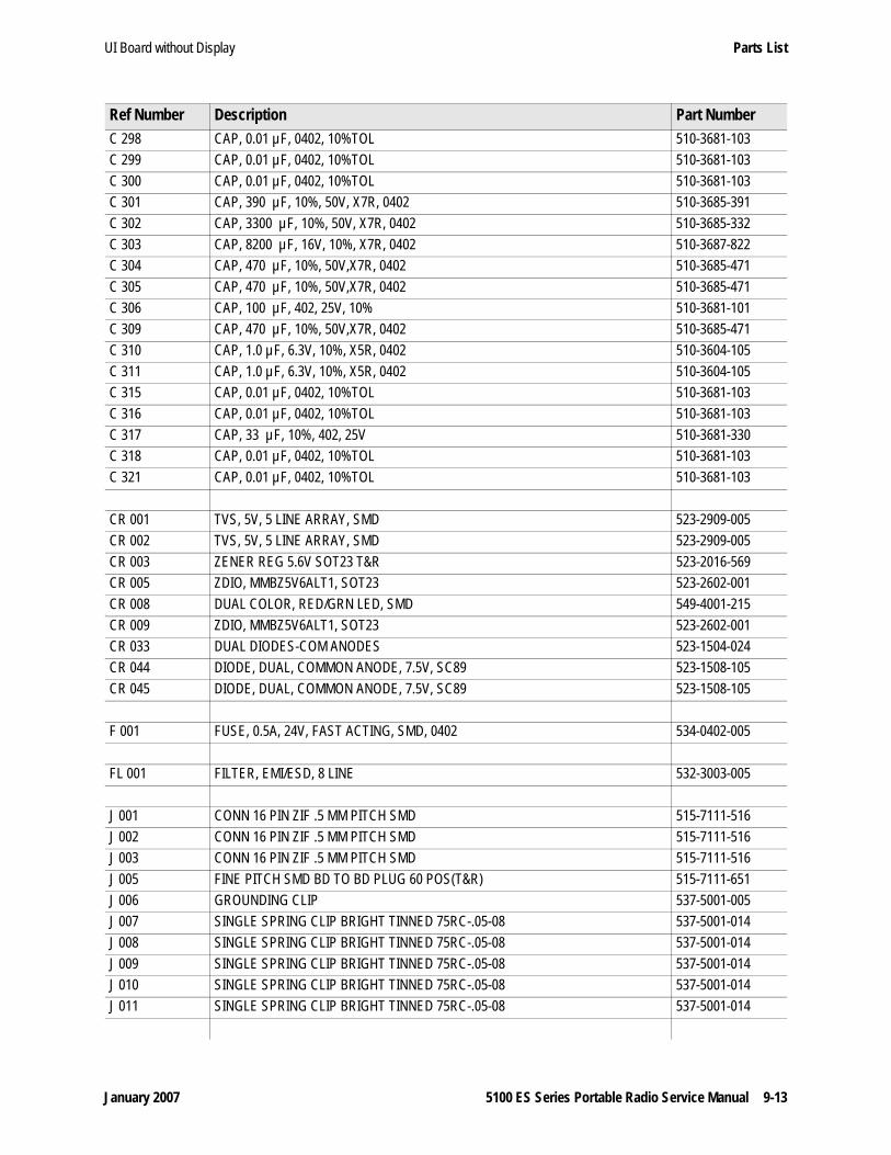
January 2007 5100 ES Series Portable Radio Service Manual 9-13
Parts ListUI Board without Display
C 298 CAP, 0.01 µF, 0402, 10%TOL 510-3681-103C 299 CAP, 0.01 µF, 0402, 10%TOL 510-3681-103C 300 CAP, 0.01 µF, 0402, 10%TOL 510-3681-103C 301 CAP, 390 µF, 10%, 50V, X7R, 0402 510-3685-391C 302 CAP, 3300 µF, 10%, 50V, X7R, 0402 510-3685-332C 303 CAP, 8200 µF, 16V, 10%, X7R, 0402 510-3687-822C 304 CAP, 470 µF, 10%, 50V,X7R, 0402 510-3685-471C 305 CAP, 470 µF, 10%, 50V,X7R, 0402 510-3685-471C 306 CAP, 100 µF, 402, 25V, 10% 510-3681-101C 309 CAP, 470 µF, 10%, 50V,X7R, 0402 510-3685-471C 310 CAP, 1.0 µF, 6.3V, 10%, X5R, 0402 510-3604-105C 311 CAP, 1.0 µF, 6.3V, 10%, X5R, 0402 510-3604-105C 315 CAP, 0.01 µF, 0402, 10%TOL 510-3681-103C 316 CAP, 0.01 µF, 0402, 10%TOL 510-3681-103C 317 CAP, 33 µF, 10%, 402, 25V 510-3681-330C 318 CAP, 0.01 µF, 0402, 10%TOL 510-3681-103C 321 CAP, 0.01 µF, 0402, 10%TOL 510-3681-103
CR 001 TVS, 5V, 5 LINE ARRAY, SMD 523-2909-005CR 002 TVS, 5V, 5 LINE ARRAY, SMD 523-2909-005CR 003 ZENER REG 5.6V SOT23 T&R 523-2016-569CR 005 ZDIO, MMBZ5V6ALT1, SOT23 523-2602-001CR 008 DUAL COLOR, RED/GRN LED, SMD 549-4001-215CR 009 ZDIO, MMBZ5V6ALT1, SOT23 523-2602-001CR 033 DUAL DIODES-COM ANODES 523-1504-024CR 044 DIODE, DUAL, COMMON ANODE, 7.5V, SC89 523-1508-105CR 045 DIODE, DUAL, COMMON ANODE, 7.5V, SC89 523-1508-105
F 001 FUSE, 0.5A, 24V, FAST ACTING, SMD, 0402 534-0402-005
FL 001 FILTER, EMI/ESD, 8 LINE 532-3003-005
J 001 CONN 16 PIN ZIF .5 MM PITCH SMD 515-7111-516J 002 CONN 16 PIN ZIF .5 MM PITCH SMD 515-7111-516J 003 CONN 16 PIN ZIF .5 MM PITCH SMD 515-7111-516J 005 FINE PITCH SMD BD TO BD PLUG 60 POS(T&R) 515-7111-651J 006 GROUNDING CLIP 537-5001-005J 007 SINGLE SPRING CLIP BRIGHT TINNED 75RC-.05-08 537-5001-014J 008 SINGLE SPRING CLIP BRIGHT TINNED 75RC-.05-08 537-5001-014J 009 SINGLE SPRING CLIP BRIGHT TINNED 75RC-.05-08 537-5001-014J 010 SINGLE SPRING CLIP BRIGHT TINNED 75RC-.05-08 537-5001-014J 011 SINGLE SPRING CLIP BRIGHT TINNED 75RC-.05-08 537-5001-014
Ref Number Description Part Number

9-14 5100 ES Series Portable Radio Service Manual January 2007
Parts List UI Board without Display
L 001 8.2 µH J CHIP L 1008 542-9000-829L 004 0.1 µH 0603 SMD INDUCTOR 542-9017-108
MP 001 SHIELD, PCB, VENTED 57851-0012-301
OSC001 OSC 20.000 MHz SMD 3.3V -40 / +85C 561-9004-200
PC 001 PCB, 5100G U BOARD 035-5500-480
Q 002 MOSFET 20V 238mA N-CH ESD SC75/SOT416, NTA4001N 576-0010-001Q 003 GEN PURPOSE 3904 BST SC-75 576-0001-029Q 004 GEN PURPOSE 3904 BST SC-75 576-0001-029Q 006 GEN PURPOSE 3904 BST SC-75 576-0001-029Q 010 MOSFET 20V 238mA N-CH ESD SC75/SOT416, NTA4001N 576-0010-001Q 012 GEN PURPOSE 3904 BST SC-75 576-0001-029Q 013 GEN PURPOSE 3904 BST SC-75 576-0001-029Q 014 GEN PURPOSE 3904 BST SC-75 576-0001-029Q 015 MOSFET 20V 238mA N-CH ESD SC75/SOT416, NTA4001N 576-0010-001Q 016 XSTR, P CHNL MOSFET, 30V, SOT23 576-0006-330Q 017 XSTR, P CHNL MOSFET, 30V, SOT23 576-0006-330
R 005 CHIP RESISTOR, 0402 569-0165-100R 055 RESISTOR 1%, 0402, 100K OHM 569-0161-501R 057 RESISTOR 1%, 0402, 100K OHM 569-0161-501R 058 RESISTOR 1%, 0402, 100K OHM 569-0161-501R 060 RES, 1K OHM, 1%, 0402 SIZE, SMT 569-0161-301R 067 RES, 47K OHM 5%, 402 569-0165-473R 075 RES, 10K, 5%, 402 569-0165-103R 076 RESISTOR, 1%, 0402, 2.21K OHM 569-0161-334R 080 RESISTOR 1%, 0402, 100K OHM 569-0161-501R 081 RESISTOR 1%, 0402, 100K OHM 569-0161-501R 083 RESISTOR 1%, 0402, 100K OHM 569-0161-501R 084 RESISTOR 1%, 0402, 4.99K 569-0161-368R 085 RESISTOR 1%, 0402, 100K OHM 569-0161-501R 086 RESISTOR 1%, 0402, 100K OHM 569-0161-501R 087 RESISTOR 1%, 0402, 49.9K OHM 569-0161-468R 088 RESISTOR 1%, 0402, 100K OHM 569-0161-501R 089 RESISTOR 1%, 0402, 100K OHM 569-0161-501R 090 RESISTOR 1%, 0402, 10K T/R 569-0161-401R 091 RESISTOR 1%, 0402, 100K OHM 569-0161-501R 095 RESISTOR 1%, 0402, 100K OHM 569-0161-501R 096 RESISTOR 1%, 0402, 100K OHM 569-0161-501R 097 75 OHMS J 063W 0603 CHIP 569-0155-750
Ref Number Description Part Number

January 2007 5100 ES Series Portable Radio Service Manual 9-15
Parts ListUI Board without Display
R 098 RES, 10K, 5%, 402 569-0165-103R 099 RES, 10K, 5%, 402 569-0165-103R 101 RES, 47K OHM 5%, 402 569-0165-473R 103 RES, 47K OHM 5%, 402 569-0165-473R 104 RES, 47K OHM 5%, 402 569-0165-473R 105 RES, 47K OHM 5%, 402 569-0165-473R 107 RESISTOR 1%, 0402, 100K OHM 569-0161-501R 111 RESISTOR 1%, 0402, 100K OHM 569-0161-501R 112 RESISTOR 1%, 0402, 100K OHM 569-0161-501R 113 RESISTOR 1%, 0402, 100K OHM 569-0161-501R 114 RESISTOR, 1%, 0402, 2.21K OHM 569-0161-334R 115 RESISTOR 1%, 0402, 49.9K OHM 569-0161-468R 116 RESISTOR 1%, 0402, 100K OHM 569-0161-501R 117 RESISTOR 1%, 0402, 100K OHM 569-0161-501R 118 RESISTOR 1%, 0402, 100K OHM 569-0161-501R 119 RESISTOR 1%, 0402, 100K OHM 569-0161-501R 120 RESISTOR 1%, 0402, 49.9K OHM 569-0161-468R 122 RESISTOR, 470 OHM, 0402, SMT 569-0165-471R 123 RESISTOR, 470 OHM, 0402, SMT 569-0165-471R 128 RESISTOR, 470 OHM, 0402, SMT 569-0165-471R 129 RESISTOR, 470 OHM, 0402, SMT 569-0165-471R 130 RES, 47K OHM 5%, 402 569-0165-473R 131 RES, 47K OHM 5%, 402 569-0165-473R 132 RES, 47K OHM 5%, 402 569-0165-473R 135 RES, 47K OHM 5%, 402 569-0165-473R 136 RES, 47K OHM 5%, 402 569-0165-473R 137 RES, 47K OHM 5%, 402 569-0165-473R 138 RES, 47K OHM 5%, 402 569-0165-473R 172 RES, 10K, 5%, 402 569-0165-103R 173 RESISTOR 1%, 0402, 100K OHM 569-0161-501R 176 75 OHMS J 063W 0603 CHIP 569-0155-750R 180 RES, 1K OHM, 1%, 0402 SIZE, SMT 569-0161-301R 244 RESISTOR 1%, 0402, 10K 569-0161-401R 252 RESISTOR 1%, 0402, 100K OHM 569-0161-501R 254 RES, 47K OHM 5%, 402 569-0165-473R 255 RESISTOR 1%, 0402, 100K OHM 569-0161-501R 256 RES, 4.7K, 5%, 402 569-0165-472R 263 RESISTOR, 1%, 0402, 2.21K OHM 569-0161-334R 269 RESISTOR, 470 OHM, 0402, SMT 569-0165-471R 278 75 OHMS J 063W 0603 CHIP 569-0155-750R 279 CHIP RESISTOR, 0402 569-0165-100R 280 RES, 4.7K, 5%, 402 569-0165-472R 281 RES, 4.7K, 5%, 402 569-0165-472
Ref Number Description Part Number

9-16 5100 ES Series Portable Radio Service Manual January 2007
Parts List UI Board without Display
R 282 RES, 10K, 5%, 402 569-0165-103R 283 RES, 10K, 5%, 402 569-0165-103R 284 RES, 1K OHM, 1%, 0402 SIZE, SMT 569-0161-301R 285 RES, 10K, 5%, 402 569-0165-103R 286 RESISTOR, 1%, 0402, 2.21K OHM 569-0161-334R 287 RES, 1K OHM, 1%, 0402 SIZE, SMT 569-0161-301R 288 RES, 10K, 5%, 402 569-0165-103R 289 RES, 10K, 5%, 402 569-0165-103R 290 RES, 10K, 5%, 402 569-0165-103R 291 RES, 10K, 5%, 402 569-0165-103R 292 RES, 10K, 5%, 402 569-0165-103R 293 RES, 10K, 5%, 402 569-0165-103R 294 RES, 10K, 5%, 402 569-0165-103R 295 RES, 1K OHM, 1%, 0402 SIZE, SMT 569-0161-301R 296 RES, 10K, 5%, 402 569-0165-103R 297 RES, 10K, 5%, 402 569-0165-103R 300 RES, 10K, 5%, 402 569-0165-103R 303 RESISTOR 1%, 0402, 100K OHM 569-0161-501R 304 RESISTOR 1%, 0402, 100K OHM 569-0161-501R 305 RES, 10K, 5%, 402 569-0165-103R 306 RES, 10K, 5%, 402 569-0165-103R 307 RES, 1K OHM, 1%, 0402 SIZE, SMT 569-0161-301R 308 RES, 10K, 5%, 402 569-0165-103R 309 RES, 10K, 5%, 402 569-0165-103R 311 RES, 10K, 5%, 402 569-0165-103R 312 RES, 10K, 5%, 402 569-0165-103R 313 RES, 10K, 5%, 402 569-0165-103R 314 RES, 10K, 5%, 402 569-0165-103R 315 RES, 10K, 5%, 402 569-0165-103R 316 RES, 10K, 5%, 402 569-0165-103R 317 RESISTOR, 470 OHM, 0402, SMT 569-0165-471R 318 RES, 10K, 5%, 402 569-0165-103R 319 RES, 10K, 5%, 402 569-0165-103R 320 CHIP RESISTOR, 0402 569-0165-100R 321 RES, 10K, 5%, 402 569-0165-103R 322 RESISTOR 1%, 0402, 100K OHM 569-0161-501R 323 RESISTOR 1%, 0402, 20K OHM 569-0161-432R 324 RESISTOR 1%, 0402, 100K OHM 569-0161-501R 325 RESISTOR 1%, 0402, 825K OHM 569-0161-589R 326 RESISTOR 1%, 0402, 10K 569-0161-401R 327 RESISTOR 1%, 0402, 6.81K OHM 569-0161-381R 328 RESISTOR 1%, 0402, 100K OHM 569-0161-501R 329 RESISTOR 1%, 0402, 4.99K 569-0161-368
Ref Number Description Part Number

January 2007 5100 ES Series Portable Radio Service Manual 9-17
Parts ListUI Board without Display
R 330 RESISTOR 1%, 0402, 100K OHM 569-0161-501R 331 RESISTOR, 1K OHM, 0402, SMT 569-0165-102R 332 RESISTOR 1%, 0402, 100K OHM 569-0161-501R 333 RES, 34K, 1%, 402 569-0161-452R 334 RES, 0 OHM 569-0155-001R 335 RESISTOR 56.2K, 1%, 0402 569-0161-473R 336 RES, 31.6K, 1%, 402 569-0161-449R 337 RES, 63.4K, 1%, 402 569-0161-478R 338 RESISTOR 1%, 0402, 4.99K 569-0161-368R 339 RESISTOR 1%, 0402, 49.9K OHM 569-0161-468R 340 RESISTOR 1%, 0402, 49.9K OHM 569-0161-468R 341 RESISTOR, 1K OHM, 0402, SMT 569-0165-102R 343 RES, 4.7K, 5%, 402 569-0165-472R 344 RES, 4.7K, 5%, 402 569-0165-472R 345 RES, 4.7K, 5%, 402 569-0165-472R 346 RES, 10K, 5%, 402 569-0165-103R 347 RES, 10K, 5%, 402 569-0165-103R 348 RES, 10K, 5%, 402 569-0165-103R 349 RES, 10K, 5%, 402 569-0165-103R 350 RES, 10K, 5%, 402 569-0165-103R 360 RES, 10K, 5%, 402 569-0165-103R 361 RES, 10K, 5%, 402 569-0165-103R 362 RES, 10K, 5%, 402 569-0165-103R 363 RES, 10K, 5%, 402 569-0165-103R 364 RES, 10K, 5%, 402 569-0165-103R 365 RES, 10K, 5%, 402 569-0165-103R 367 RES, 10K, 5%, 402 569-0165-103R 376 RESISTOR, 255K, 1%, 0402 569-0161-540R 377 RES, 10K, 5%, 402 569-0165-103R 378 RESISTOR 1%, 0402, 100K OHM 569-0161-501R 379 RES, 10K, 5%, 402 569-0165-103R 380 CHIP RESISTOR, 0402 569-0165-100R 381 CHIP RESISTOR, 0402 569-0165-100R 382 RES, 31.6K, 1%, 402 569-0161-449R 383 RES, 10K, 5%, 402 569-0165-103R 384 RES, 10K, 5%, 402 569-0165-103R 385 RES, 10K, 5%, 402 569-0165-103R 386 RES, 34K, 1%, 402 569-0161-452R 387 RESISTOR 1%, 0402, 49.9K OHM 569-0161-468R 388 RES, 10K, 5%, 402 569-0165-103R 389 RES, 10K, 5%, 402 569-0165-103R 390 RES, 10K, 5%, 402 569-0165-103R 391 RESISTOR, 1K OHM, 0402, SMT 569-0165-102
Ref Number Description Part Number
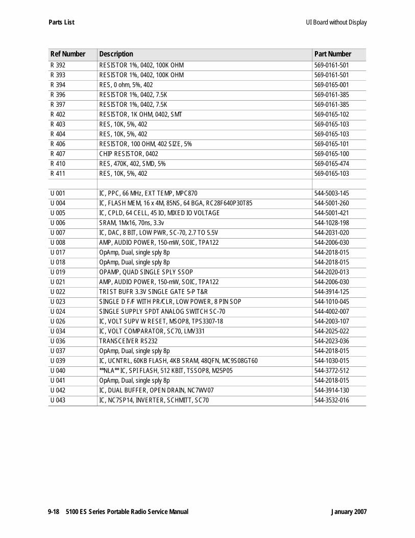
9-18 5100 ES Series Portable Radio Service Manual January 2007
Parts List UI Board without Display
R 392 RESISTOR 1%, 0402, 100K OHM 569-0161-501R 393 RESISTOR 1%, 0402, 100K OHM 569-0161-501R 394 RES, 0 ohm, 5%, 402 569-0165-001R 396 RESISTOR 1%, 0402, 7.5K 569-0161-385R 397 RESISTOR 1%, 0402, 7.5K 569-0161-385R 402 RESISTOR, 1K OHM, 0402, SMT 569-0165-102R 403 RES, 10K, 5%, 402 569-0165-103R 404 RES, 10K, 5%, 402 569-0165-103R 406 RESISTOR, 100 OHM, 402 SIZE, 5% 569-0165-101R 407 CHIP RESISTOR, 0402 569-0165-100R 410 RES, 470K, 402, SMD, 5% 569-0165-474R 411 RES, 10K, 5%, 402 569-0165-103
U 001 IC, PPC, 66 MHz, EXT TEMP, MPC870 544-5003-145U 004 IC, FLASH MEM, 16 x 4M, 85NS, 64 BGA, RC28F640P30T85 544-5001-260U 005 IC, CPLD, 64 CELL, 45 IO, MIXED IO VOLTAGE 544-5001-421U 006 SRAM, 1Mx16, 70ns, 3.3v 544-1028-198U 007 IC, DAC, 8 BIT, LOW PWR, SC-70, 2.7 TO 5.5V 544-2031-020U 008 AMP, AUDIO POWER, 150-mW, SOIC, TPA122 544-2006-030U 017 OpAmp, Dual, single sply 8p 544-2018-015U 018 OpAmp, Dual, single sply 8p 544-2018-015U 019 OPAMP, QUAD SINGLE SPLY SSOP 544-2020-013U 021 AMP, AUDIO POWER, 150-mW, SOIC, TPA122 544-2006-030U 022 TRI ST BUFR 3.3V SINGLE GATE 5-P T&R 544-3914-125U 023 SINGLE D F/F WITH PR/CLR, LOW POWER, 8 PIN SOP 544-1010-045U 024 SINGLE SUPPLY SPDT ANALOG SWITCH SC-70 544-4002-007U 026 IC, VOLT SUPV W RESET, MSOP8, TPS3307-18 544-2003-107U 034 IC, VOLT COMPARATOR, SC70, LMV331 544-2025-022U 036 TRANSCEIVER RS232 544-2023-036U 037 OpAmp, Dual, single sply 8p 544-2018-015U 039 IC, UCNTRL, 60KB FLASH, 4KB SRAM, 48QFN, MC9S08GT60 544-1030-015U 040 **NLA** IC, SPI FLASH, 512 KBIT, TSSOP8, M25P05 544-3772-512U 041 OpAmp, Dual, single sply 8p 544-2018-015U 042 IC, DUAL BUFFER, OPEN DRAIN, NC7WV07 544-3914-130U 043 IC, NC7SP14, INVERTER, SCHMITT, SC70 544-3532-016
Ref Number Description Part Number

January 2007 5100 ES Series Portable Radio Service Manual 9-19
Parts List5100G UI Bd, w/o Display, Non-FM
Ref Number Description Part Number5100G UI Bd, w/o Display, Non-FM(Eff Begin 01-11-07)
023-5500-487
C 013 CAP, 100 pF, 402, 25V, 10% 510-3681-101C 014 CAP, 100 pF, 402, 25V, 10% 510-3681-101C 029 CERAMIC CAPACITOR, 10 µF, 1206,10V 510-3755-106C 030 CAP, 0.1 µF, 16V, 10%, X7R, 0402 (t&r) 510-3687-104C 035 CAP, 0.1 µF, 16V, 10%, X7R, 0402 (t&r) 510-3687-104C 036 CAP, 0.01 µF, 0402, 10%TOL 510-3681-103C 044 CAP, 0.1 µF, 16V, 10%, X7R, 0402 (t&r) 510-3687-104C 047 CAP, 680 pF, 10%, 50V, X7R, 0402 (t&r) 510-3685-681C 053 CAP, 100 pF, 402, 25V, 10% 510-3681-101C 054 CAP, 100 pF, 402, 25V, 10% 510-3681-101C 071 CAP, 0.01 µF, 0402, 10%TOL 510-3681-103C 072 CAP, 0.1 µF, 16V, 10%, X7R, 0402 (t&r) 510-3687-104C 076 CAP, 22 µF, 16V, 20%, X5R, 1206 510-3804-226C 077 CAP, 10 µF, 16V, 10%, X5R, 0805 510-3803-106C 078 CAP, 0.1 µF, 16V, 10%, X7R, 0402 (t&r) 510-3687-104C 079 CAP, 0.1 µF, 16V, 10%, X7R, 0402 (t&r) 510-3687-104C 080 CAP, 0.1 µF, 16V, 10%, X7R, 0402 (t&r) 510-3687-104C 083 CAP, 0.1 µF, 16V, 10%, X7R, 0402 (t&r) 510-3687-104C 084 CAP, 0.01 µF, 0402, 10%TOL 510-3681-103C 086 CAP, 0.01 µF, 0402, 10%TOL 510-3681-103C 087 CAP, 0.01 µF, 0402, 10%TOL 510-3681-103C 088 CAP, 22 µF, 16V, 20%, X5R, 1206 510-3804-226C 089 CAP, 220 pF, 10%, 50V, X7R, 0402 (t&r) 510-3685-221C 092 CAP, 0.1 µF, 16V, 10%, X7R, 0402 (t&r) 510-3687-104C 093 CAP, 0.1 µF, 16V, 10%, X7R, 0402 (t&r) 510-3687-104C 094 CAP, 0.1 µF, 16V, 10%, X7R, 0402 (t&r) 510-3687-104C 095 CAP, 1 µF, 25V, 0603, X5S, +/-20% 510-3693-105C 097 CAP, 0.1 µF, 16V, 10%, X7R, 0402 (t&r) 510-3687-104C 098 CAP, 0.1 µF, 16V, 10%, X7R, 0402 (t&r) 510-3687-104C 099 CAP, 0.1 µF, 16V, 10%, X7R, 0402 (t&r) 510-3687-104C 100 CAP, 2200 pF, 0402, SMD, 10V, 10% 510-3681-222C 101 CAP, 270 pF, 10%, 50V, X7R, 0402 (t&r) 510-3685-271C 112 CAP, 0.01 µF, 0402, 10%TOL 510-3681-103C 133 CAP, 470 pF, 10%, 50V,X7R,0402 510-3685-471C 134 CAP, 0.1 µF, 16V, 10%, X7R, 0402 (t&r) 510-3687-104C 135 CAP, 0.1 µF, 16V, 10%, X7R, 0402 (t&r) 510-3687-104C 136 CAP, 0.1 µF, 16V, 10%, X7R, 0402 (t&r) 510-3687-104C 137 CAP, 0.1 µF, 16V, 10%, X7R, 0402 (t&r) 510-3687-104C 139 CAP, 100 pF, 402, 25V, 10% 510-3681-101C 140 CAP, 100 pF, 402, 25V, 10% 510-3681-101

9-20 5100 ES Series Portable Radio Service Manual January 2007
Parts List 5100G UI Bd, w/o Display, Non-FM
C 142 CAP, 100 pF, 402, 25V, 10% 510-3681-101C 143 CAP, 100 pF, 402, 25V, 10% 510-3681-101C 144 CAP, 100 pF, 402, 25V, 10% 510-3681-101C 158 CAP, 0.01 µF, 0402, 10%TOL 510-3681-103C 164 CAP, 100 pF, 402, 25V, 10% 510-3681-101C 165 CAP, 100 pF, 402, 25V, 10% 510-3681-101C 166 CAP, 100 pF, 402, 25V, 10% 510-3681-101C 167 CAP, 100 pF, 402, 25V, 10% 510-3681-101C 168 CAP, 100 pF, 402, 25V, 10% 510-3681-101C 169 CAP, 100 pF, 402, 25V, 10% 510-3681-101C 172 CAP, 100 pF, 402, 25V, 10% 510-3681-101C 173 CAP, 100 pF, 402, 25V, 10% 510-3681-101C 174 CAP, 100 pF, 402, 25V, 10% 510-3681-101C 175 CAP, 100 pF, 402, 25V, 10% 510-3681-101C 176 CAP, 100 pF, 402, 25V, 10% 510-3681-101C 177 CAP, 100 pF, 402, 25V, 10% 510-3681-101C 202 CAP, 470 pF, 10%, 50V,X7R,0402 510-3685-471C 215 CAP, 470 pF, 10%, 50V,X7R,0402 510-3685-471C 216 CAP, 470 pF, 10%, 50V,X7R,0402 510-3685-471C 217 CAP, 470 pF, 10%, 50V,X7R,0402 510-3685-471C 220 CAP, 470 pF, 10%, 50V,X7R,0402 510-3685-471C 221 CAP, 470 pF, 10%, 50V,X7R,0402 510-3685-471C 222 CAP, 0.1 µF, 16V, 10%, X7R, 0402 (t&r) 510-3687-104C 223 CAP, 100 pF, 402, 25V, 10% 510-3681-101C 224 CAP, 100 pF, 402, 25V, 10% 510-3681-101C 226 CAP, 0.01 µF, 0402, 10%TOL 510-3681-103C 227 CAP, 0.01 µF, 0402, 10%TOL 510-3681-103C 228 CAP, 0.01 µF, 0402, 10%TOL 510-3681-103C 229 CAP, 0.1 µF, 16V, 10%, X7R, 0402 (t&r) 510-3687-104C 230 CAP, 0.1 µF, 16V, 10%, X7R, 0402 (t&r) 510-3687-104C 231 CAP, 0.01 µF, 0402, 10%TOL 510-3681-103C 232 CAP, 0.01 µF, 0402, 10%TOL 510-3681-103C 233 CAP, 0.01 µF, 0402, 10%TOL 510-3681-103C 234 CAP, 0.1 µF, 16V, 10%, X7R, 0402 (t&r) 510-3687-104C 235 CAP, 0.1 µF, 16V, 10%, X7R, 0402 (t&r) 510-3687-104C 236 CAP, 0.01 µF, 0402, 10%TOL 510-3681-103C 237 CAP, 0.01 µF, 0402, 10%TOL 510-3681-103C 238 CAP, 0.01 µF, 0402, 10%TOL 510-3681-103C 239 CAP, 0.01 µF, 0402, 10%TOL 510-3681-103C 240 CAP, 0.01 µF, 0402, 10%TOL 510-3681-103C 241 CAP, 0.1 µF, 16V, 10%, X7R, 0402 (t&r) 510-3687-104C 242 CAP, 0.1 µF, 16V, 10%, X7R, 0402 (t&r) 510-3687-104C 243 CAP, 0.1 µF, 16V, 10%, X7R, 0402 (t&r) 510-3687-104
Ref Number Description Part Number

January 2007 5100 ES Series Portable Radio Service Manual 9-21
Parts List5100G UI Bd, w/o Display, Non-FM
C 244 CAP, 0.1 µF, 16V, 10%, X7R, 0402 (t&r) 510-3687-104C 245 CAP, 0.1 µF, 16V, 10%, X7R, 0402 (t&r) 510-3687-104C 246 CAP, 0.01 µF, 0402, 10%TOL 510-3681-103C 247 CAP, 0.1 µF, 16V, 10%, X7R, 0402 (t&r) 510-3687-104C 248 CAP, 0.01 µF, 0402, 10%TOL 510-3681-103C 249 CAP, 0.01 µF, 0402, 10%TOL 510-3681-103C 250 CAP, 0.01 µF, 0402, 10%TOL 510-3681-103C 251 CAP, 0.01 µF, 0402, 10%TOL 510-3681-103C 252 CAP, 0.1 µF, 16V, 10%, X7R, 0402 (t&r) 510-3687-104C 253 CAP, 0.1 µF, 16V, 10%, X7R, 0402 (t&r) 510-3687-104C 254 CAP, 0.01 µF, 0402, 10%TOL 510-3681-103C 255 CAP, 0.01 µF, 0402, 10%TOL 510-3681-103C 256 CAP, 0.01 µF, 0402, 10%TOL 510-3681-103C 257 CAP, 0.01 µF, 0402, 10%TOL 510-3681-103C 258 CAP, 0.01 µF, 0402, 10%TOL 510-3681-103C 259 CAP, 0.01 µF, 0402, 10%TOL 510-3681-103C 260 CAP, 0.01 µF, 0402, 10%TOL 510-3681-103C 261 1000 pF, 50V, 0402 CERAMIC CAP, X7R, +/-10% 510-3685-102C 263 CAP, 1.0 µF, 6.3V, 10%, X5R, 0402 510-3604-105C 265 CAP, 0.01 µF, 0402, 10%TOL 510-3681-103C 266 CAP, 0.01 µF, 0402, 10%TOL 510-3681-103C 267 CAP, 470 pF, 10%, 50V,X7R,0402 510-3685-471C 268 CAP, 470 pF, 10%, 50V,X7R,0402 510-3685-471C 269 CAP, 680 pF, 10%, 50V, X7R, 0402 (t&r) 510-3685-681C 270 CAP, 470 pF, 10%, 50V,X7R,0402 510-3685-471C 271 CAP, 470 pF, 10%, 50V,X7R,0402 510-3685-471C 272 CAP, 470 pF, 10%, 50V,X7R,0402 510-3685-471C 273 CAP, 470 pF, 10%, 50V,X7R,0402 510-3685-471C 274 CAP, 0.01 µF, 0402, 10%TOL 510-3681-103C 275 CAP, 0.01 µF, 0402, 10%TOL 510-3681-103C 276 CAP, 100 pF, 402, 25V, 10% 510-3681-101C 277 CAP, 100 pF, 402, 25V, 10% 510-3681-101C 278 CAP, 100 pF, 402, 25V, 10% 510-3681-101C 279 CAP, 100 pF, 402, 25V, 10% 510-3681-101C 280 CAP, 100 pF, 402, 25V, 10% 510-3681-101C 281 CAP, 100 pF, 402, 25V, 10% 510-3681-101C 282 CAP, 100 pF, 402, 25V, 10% 510-3681-101C 283 CAP, 100 pF, 402, 25V, 10% 510-3681-101C 284 CAP, 100 pF, 402, 25V, 10% 510-3681-101C 285 CAP, 100 pF, 402, 25V, 10% 510-3681-101C 286 CAP, 100 pF, 402, 25V, 10% 510-3681-101C 287 CAP, 100 pF, 402, 25V, 10% 510-3681-101C 288 CAP, 0.01 µF, 0402, 10%TOL 510-3681-103
Ref Number Description Part Number
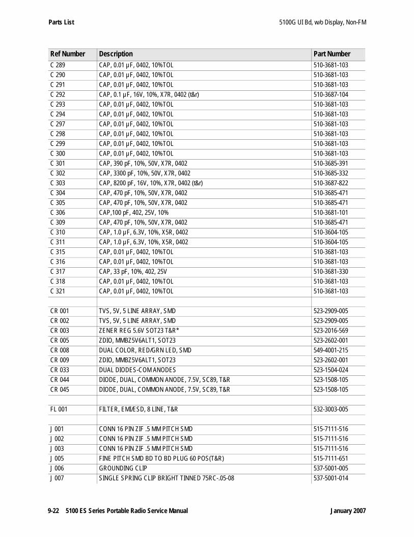
9-22 5100 ES Series Portable Radio Service Manual January 2007
Parts List 5100G UI Bd, w/o Display, Non-FM
C 289 CAP, 0.01 µF, 0402, 10%TOL 510-3681-103C 290 CAP, 0.01 µF, 0402, 10%TOL 510-3681-103C 291 CAP, 0.01 µF, 0402, 10%TOL 510-3681-103C 292 CAP, 0.1 µF, 16V, 10%, X7R, 0402 (t&r) 510-3687-104C 293 CAP, 0.01 µF, 0402, 10%TOL 510-3681-103C 294 CAP, 0.01 µF, 0402, 10%TOL 510-3681-103C 297 CAP, 0.01 µF, 0402, 10%TOL 510-3681-103C 298 CAP, 0.01 µF, 0402, 10%TOL 510-3681-103C 299 CAP, 0.01 µF, 0402, 10%TOL 510-3681-103C 300 CAP, 0.01 µF, 0402, 10%TOL 510-3681-103C 301 CAP, 390 pF, 10%, 50V, X7R, 0402 510-3685-391C 302 CAP, 3300 pF, 10%, 50V, X7R, 0402 510-3685-332C 303 CAP, 8200 pF, 16V, 10%, X7R, 0402 (t&r) 510-3687-822C 304 CAP, 470 pF, 10%, 50V, X7R, 0402 510-3685-471C 305 CAP, 470 pF, 10%, 50V, X7R, 0402 510-3685-471C 306 CAP,100 pF, 402, 25V, 10% 510-3681-101C 309 CAP, 470 pF, 10%, 50V, X7R, 0402 510-3685-471C 310 CAP, 1.0 µF, 6.3V, 10%, X5R, 0402 510-3604-105C 311 CAP, 1.0 µF, 6.3V, 10%, X5R, 0402 510-3604-105C 315 CAP, 0.01 µF, 0402, 10%TOL 510-3681-103C 316 CAP, 0.01 µF, 0402, 10%TOL 510-3681-103C 317 CAP, 33 pF, 10%, 402, 25V 510-3681-330C 318 CAP, 0.01 µF, 0402, 10%TOL 510-3681-103C 321 CAP, 0.01 µF, 0402, 10%TOL 510-3681-103
CR 001 TVS, 5V, 5 LINE ARRAY, SMD 523-2909-005CR 002 TVS, 5V, 5 LINE ARRAY, SMD 523-2909-005CR 003 ZENER REG 5.6V SOT23 T&R* 523-2016-569CR 005 ZDIO, MMBZ5V6ALT1, SOT23 523-2602-001CR 008 DUAL COLOR, RED/GRN LED, SMD 549-4001-215CR 009 ZDIO, MMBZ5V6ALT1, SOT23 523-2602-001CR 033 DUAL DIODES-COM ANODES 523-1504-024CR 044 DIODE, DUAL, COMMON ANODE, 7.5V, SC89, T&R 523-1508-105CR 045 DIODE, DUAL, COMMON ANODE, 7.5V, SC89, T&R 523-1508-105
FL 001 FILTER, EMI/ESD, 8 LINE, T&R 532-3003-005
J 001 CONN 16 PIN ZIF .5 MM PITCH SMD 515-7111-516J 002 CONN 16 PIN ZIF .5 MM PITCH SMD 515-7111-516J 003 CONN 16 PIN ZIF .5 MM PITCH SMD 515-7111-516J 005 FINE PITCH SMD BD TO BD PLUG 60 POS(T&R) 515-7111-651J 006 GROUNDING CLIP 537-5001-005J 007 SINGLE SPRING CLIP BRIGHT TINNED 75RC-.05-08 537-5001-014
Ref Number Description Part Number

January 2007 5100 ES Series Portable Radio Service Manual 9-23
Parts List5100G UI Bd, w/o Display, Non-FM
J 008 SINGLE SPRING CLIP BRIGHT TINNED 75RC-.05-08 537-5001-014J 009 SINGLE SPRING CLIP BRIGHT TINNED 75RC-.05-08 537-5001-014J 010 SINGLE SPRING CLIP BRIGHT TINNED 75RC-.05-08 537-5001-014J 011 SINGLE SPRING CLIP BRIGHT TINNED 75RC-.05-08 537-5001-014
L 001 8.2 µH J CHIP L 1008 542-9000-829L 004 0.1 µH 0603 SMD INDUCTOR (T&R) 542-9017-108
MP 001 SHIELD, PCB, VENTED 578-5100-12301
OSC001 OSC 20.000 MHz SMD 3.3V -40 / +85C 561-9004-200
PC 001 PCB, 5100G UI BOARD (REV 1) 355-5004-8001
Q 002 MOSFET 20V 238mA N-CH ESD SC75/SOT416, NTA4001N 576-0010-001Q 003 GEN PURPOSE 3904 BST SC-75 576-0001-029Q 004 GEN PURPOSE 3904 BST SC-75 576-0001-029Q 006 GEN PURPOSE 3904 BST SC-75 576-0001-029Q 010 MOSFET 20V 238mA N-CH ESD SC75/SOT416, NTA4001N 576-0010-001Q 012 GEN PURPOSE 3904 BST SC-75 576-0001-029Q 013 GEN PURPOSE 3904 BST SC-75 576-0001-029Q 014 GEN PURPOSE 3904 BST SC-75 576-0001-029Q 015 MOSFET 20V 238mA N-CH ESD SC75/SOT416, NTA4001N 576-0010-001Q 016 XSTR, P CHNL MOSFET, 30V, SOT23 576-0006-330Q 017 XSTR, P CHNL MOSFET, 30V, SOT23 576-0006-330
R 005 CHIP RESISTOR, TAPE & REEL, 0402 569-0165-100R 055 RESISTOR 1%, 0402, 100K OHM 569-0161-501R 057 RESISTOR 1%, 0402, 100K OHM 569-0161-501R 058 RESISTOR 1%, 0402, 100K OHM 569-0161-501R 060 RES, 1K OHM, 1%, 0402 SIZE, SMT 569-0161-301R 067 RES,47K OHM 5%, 402 569-0165-473R 075 RES, 10K, 5%, 402 569-0165-103R 076 RESISTOR, 1%, 0402, 2.21K OHM 569-0161-334R 080 RESISTOR 1%, 0402, 100K OHM 569-0161-501R 081 RESISTOR 1%, 0402, 100K OHM 569-0161-501R 083 RESISTOR 1%, 0402, 100K OHM 569-0161-501R 084 RESISTOR 1%, 0402, 4.99K, T&R 569-0161-368R 085 RESISTOR 1%, 0402, 100K OHM 569-0161-501R 086 RESISTOR 1%, 0402, 100K OHM 569-0161-501R 087 RESISTOR 1%, 0402, 49.9K OHM, T&R 569-0161-468R 088 RESISTOR 1%, 0402, 100K OHM 569-0161-501R 089 RESISTOR 1%, 0402, 100K OHM 569-0161-501
Ref Number Description Part Number
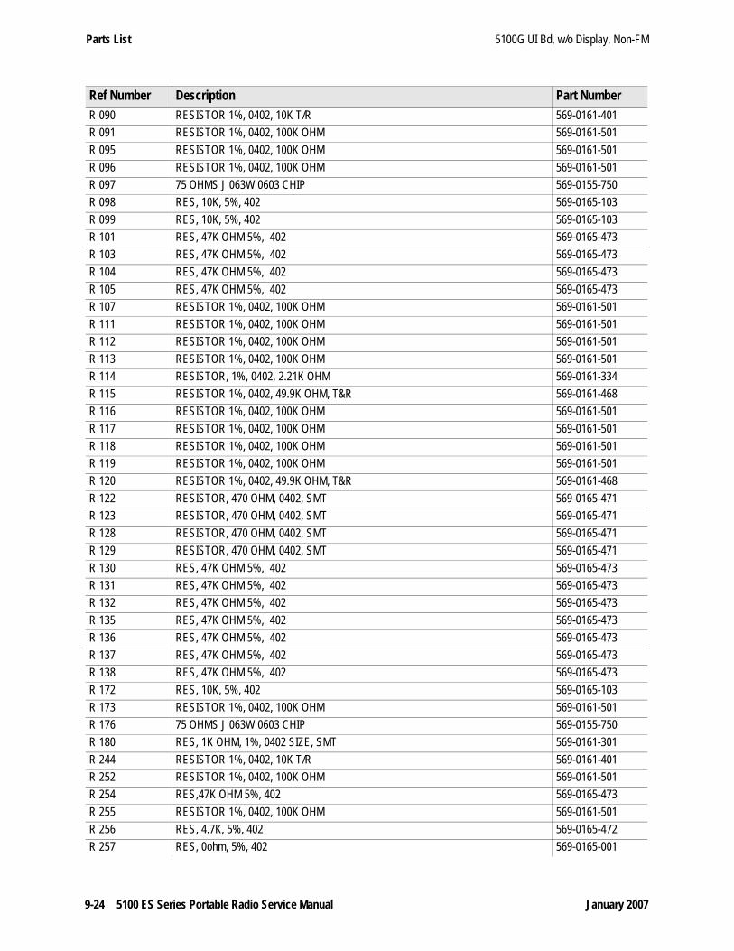
9-24 5100 ES Series Portable Radio Service Manual January 2007
Parts List 5100G UI Bd, w/o Display, Non-FM
R 090 RESISTOR 1%, 0402, 10K T/R 569-0161-401R 091 RESISTOR 1%, 0402, 100K OHM 569-0161-501R 095 RESISTOR 1%, 0402, 100K OHM 569-0161-501R 096 RESISTOR 1%, 0402, 100K OHM 569-0161-501R 097 75 OHMS J 063W 0603 CHIP 569-0155-750R 098 RES, 10K, 5%, 402 569-0165-103R 099 RES, 10K, 5%, 402 569-0165-103R 101 RES, 47K OHM 5%, 402 569-0165-473R 103 RES, 47K OHM 5%, 402 569-0165-473R 104 RES, 47K OHM 5%, 402 569-0165-473R 105 RES, 47K OHM 5%, 402 569-0165-473R 107 RESISTOR 1%, 0402, 100K OHM 569-0161-501R 111 RESISTOR 1%, 0402, 100K OHM 569-0161-501R 112 RESISTOR 1%, 0402, 100K OHM 569-0161-501R 113 RESISTOR 1%, 0402, 100K OHM 569-0161-501R 114 RESISTOR, 1%, 0402, 2.21K OHM 569-0161-334R 115 RESISTOR 1%, 0402, 49.9K OHM, T&R 569-0161-468R 116 RESISTOR 1%, 0402, 100K OHM 569-0161-501R 117 RESISTOR 1%, 0402, 100K OHM 569-0161-501R 118 RESISTOR 1%, 0402, 100K OHM 569-0161-501R 119 RESISTOR 1%, 0402, 100K OHM 569-0161-501R 120 RESISTOR 1%, 0402, 49.9K OHM, T&R 569-0161-468R 122 RESISTOR, 470 OHM, 0402, SMT 569-0165-471R 123 RESISTOR, 470 OHM, 0402, SMT 569-0165-471R 128 RESISTOR, 470 OHM, 0402, SMT 569-0165-471R 129 RESISTOR, 470 OHM, 0402, SMT 569-0165-471R 130 RES, 47K OHM 5%, 402 569-0165-473R 131 RES, 47K OHM 5%, 402 569-0165-473R 132 RES, 47K OHM 5%, 402 569-0165-473R 135 RES, 47K OHM 5%, 402 569-0165-473R 136 RES, 47K OHM 5%, 402 569-0165-473R 137 RES, 47K OHM 5%, 402 569-0165-473R 138 RES, 47K OHM 5%, 402 569-0165-473R 172 RES, 10K, 5%, 402 569-0165-103R 173 RESISTOR 1%, 0402, 100K OHM 569-0161-501R 176 75 OHMS J 063W 0603 CHIP 569-0155-750R 180 RES, 1K OHM, 1%, 0402 SIZE, SMT 569-0161-301R 244 RESISTOR 1%, 0402, 10K T/R 569-0161-401R 252 RESISTOR 1%, 0402, 100K OHM 569-0161-501R 254 RES,47K OHM 5%, 402 569-0165-473R 255 RESISTOR 1%, 0402, 100K OHM 569-0161-501R 256 RES, 4.7K, 5%, 402 569-0165-472R 257 RES, 0ohm, 5%, 402 569-0165-001
Ref Number Description Part Number

January 2007 5100 ES Series Portable Radio Service Manual 9-25
Parts List5100G UI Bd, w/o Display, Non-FM
R 263 RESISTOR, 1%, 0402, 2.21K OHM 569-0161-334R 269 RESISTOR, 470 OHM, 0402, SMT 569-0165-471R 278 75 OHMS J 063W 0603 CHIP 569-0155-750R 279 CHIP RESISTOR, TAPE & REEL, 0402 569-0165-100R 280 RES, 4.7K, 5%, 402 569-0165-472R 281 RES, 4.7K, 5%, 402 569-0165-472R 282 RES, 10K, 5%, 402 569-0165-103R 283 RES, 10K, 5%, 402 569-0165-103R 284 RES, 1K OHM, 1%, 0402 SIZE, SMT 569-0161-301R 285 RES, 10K, 5%, 402 569-0165-103R 286 RESISTOR, 1%, 0402, 2.21K OHM 569-0161-334R 287 RES, 1K OHM, 1%, 0402 SIZE, SMT 569-0161-301R 288 RES, 10K, 5%, 402 569-0165-103R 289 RES, 10K, 5%, 402 569-0165-103R 290 RES, 10K, 5%, 402 569-0165-103R 291 RES, 10K, 5%, 402 569-0165-103R 292 RES, 10K, 5%, 402 569-0165-103R 293 RES, 10K, 5%, 402 569-0165-103R 294 RES, 10K, 5%, 402 569-0165-103R 295 RES, 1K OHM, 1%, 0402 SIZE, SMT 569-0161-301R 296 RES, 10K, 5%, 402 569-0165-103R 297 RES, 10K, 5%, 402 569-0165-103R 300 RES, 10K, 5%, 402 569-0165-103R 303 RESISTOR 1%, 0402, 100K OHM 569-0161-501R 304 RESISTOR 1%, 0402, 100K OHM 569-0161-501R 305 RES, 10K, 5%, 402 569-0165-103R 306 RES, 10K, 5%, 402 569-0165-103R 307 RES, 1K OHM, 1%, 0402 SIZE, SMT 569-0161-301R 308 RES, 10K, 5%, 402 569-0165-103R 309 RES, 10K, 5%, 402 569-0165-103R 311 RES, 10K, 5%, 402 569-0165-103R 312 RES, 10K, 5%, 402 569-0165-103R 313 RES, 10K, 5%, 402 569-0165-103R 314 RES, 10K, 5%, 402 569-0165-103R 315 RES, 10K, 5%, 402 569-0165-103R 316 RES, 10K, 5%, 402 569-0165-103R 317 RESISTOR, 470 OHM, 0402, SMT 569-0165-471R 318 RES, 10K, 5%, 402 569-0165-103R 319 RES, 10K, 5%, 402 569-0165-103R 320 CHIP RESISTOR, TAPE & REEL, 0402 569-0165-100R 321 RES, 10K, 5%, 402 569-0165-103R 322 RESISTOR 1%, 0402, 100K OHM 569-0161-501R 323 RESISTOR 1%, 0402, 20K OHM, T&R 569-0161-432
Ref Number Description Part Number
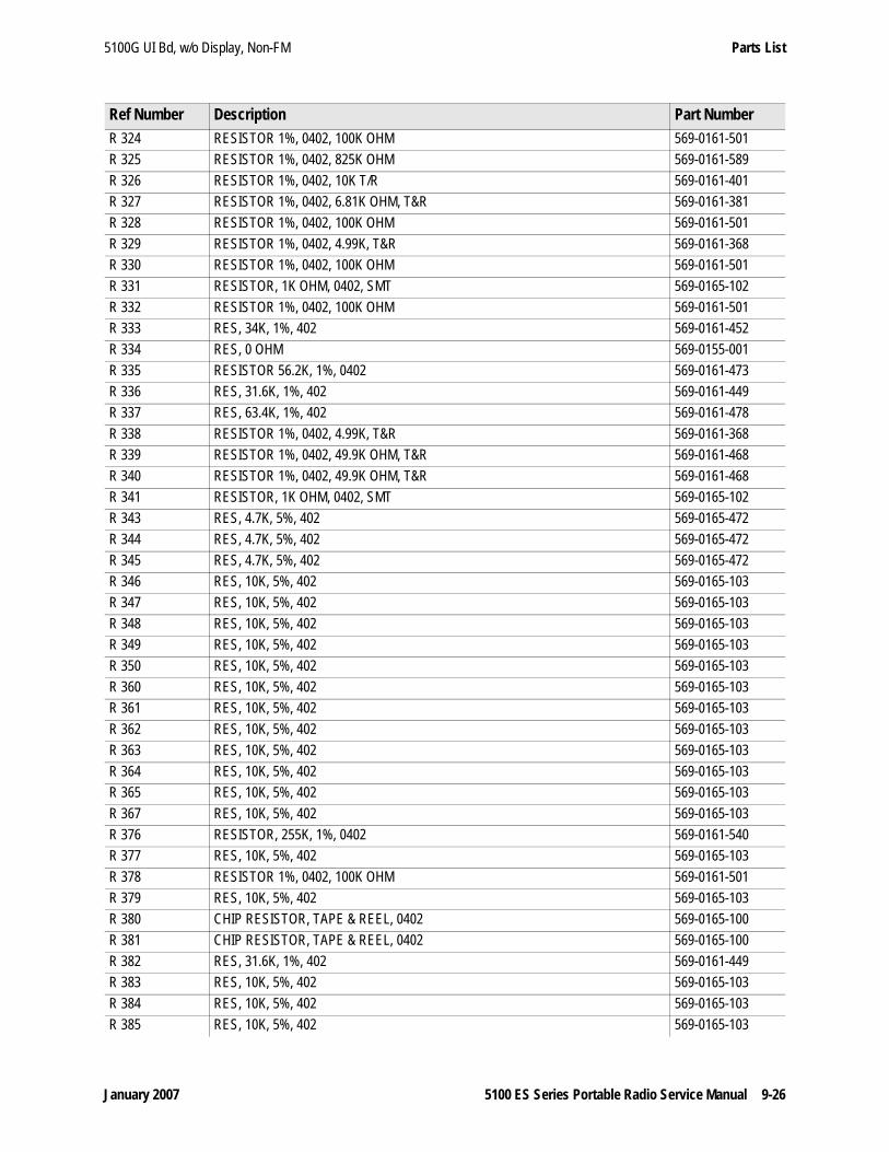
January 2007 5100 ES Series Portable Radio Service Manual 9-26
Parts List5100G UI Bd, w/o Display, Non-FM
R 324 RESISTOR 1%, 0402, 100K OHM 569-0161-501R 325 RESISTOR 1%, 0402, 825K OHM 569-0161-589R 326 RESISTOR 1%, 0402, 10K T/R 569-0161-401R 327 RESISTOR 1%, 0402, 6.81K OHM, T&R 569-0161-381R 328 RESISTOR 1%, 0402, 100K OHM 569-0161-501R 329 RESISTOR 1%, 0402, 4.99K, T&R 569-0161-368R 330 RESISTOR 1%, 0402, 100K OHM 569-0161-501R 331 RESISTOR, 1K OHM, 0402, SMT 569-0165-102R 332 RESISTOR 1%, 0402, 100K OHM 569-0161-501R 333 RES, 34K, 1%, 402 569-0161-452R 334 RES, 0 OHM 569-0155-001R 335 RESISTOR 56.2K, 1%, 0402 569-0161-473R 336 RES, 31.6K, 1%, 402 569-0161-449R 337 RES, 63.4K, 1%, 402 569-0161-478R 338 RESISTOR 1%, 0402, 4.99K, T&R 569-0161-368R 339 RESISTOR 1%, 0402, 49.9K OHM, T&R 569-0161-468R 340 RESISTOR 1%, 0402, 49.9K OHM, T&R 569-0161-468R 341 RESISTOR, 1K OHM, 0402, SMT 569-0165-102R 343 RES, 4.7K, 5%, 402 569-0165-472R 344 RES, 4.7K, 5%, 402 569-0165-472R 345 RES, 4.7K, 5%, 402 569-0165-472R 346 RES, 10K, 5%, 402 569-0165-103R 347 RES, 10K, 5%, 402 569-0165-103R 348 RES, 10K, 5%, 402 569-0165-103R 349 RES, 10K, 5%, 402 569-0165-103R 350 RES, 10K, 5%, 402 569-0165-103R 360 RES, 10K, 5%, 402 569-0165-103R 361 RES, 10K, 5%, 402 569-0165-103R 362 RES, 10K, 5%, 402 569-0165-103R 363 RES, 10K, 5%, 402 569-0165-103R 364 RES, 10K, 5%, 402 569-0165-103R 365 RES, 10K, 5%, 402 569-0165-103R 367 RES, 10K, 5%, 402 569-0165-103R 376 RESISTOR, 255K, 1%, 0402 569-0161-540R 377 RES, 10K, 5%, 402 569-0165-103R 378 RESISTOR 1%, 0402, 100K OHM 569-0161-501R 379 RES, 10K, 5%, 402 569-0165-103R 380 CHIP RESISTOR, TAPE & REEL, 0402 569-0165-100R 381 CHIP RESISTOR, TAPE & REEL, 0402 569-0165-100R 382 RES, 31.6K, 1%, 402 569-0161-449R 383 RES, 10K, 5%, 402 569-0165-103R 384 RES, 10K, 5%, 402 569-0165-103R 385 RES, 10K, 5%, 402 569-0165-103
Ref Number Description Part Number

January 2007 5100 ES Series Portable Radio Service Manual 9-27
Parts List
R 386 RES, 34K, 1%, 402 569-0161-452R 387 RESISTOR 1%, 0402, 49.9K OHM, T&R 569-0161-468R 388 RES, 10K, 5%, 402 569-0165-103R 389 RES, 10K, 5%, 402 569-0165-103R 390 RES, 10K, 5%, 402 569-0165-103R 391 RESISTOR, 1K OHM, 0402, SMT 569-0165-102R 392 RESISTOR 1%, 0402, 100K OHM 569-0161-501R 393 RESISTOR 1%, 0402, 100K OHM 569-0161-501R 394 RES, 0ohm, 5%, 402 569-0165-001R 396 RESISTOR 1%, 0402, 7.5K, T&R 569-0161-385R 397 RESISTOR 1%, 0402, 7.5K, T&R 569-0161-385R 402 RESISTOR, 1K OHM, 0402, SMT 569-0165-102R 403 RES, 10K, 5%, 402 569-0165-103R 404 RES, 10K, 5%, 402 569-0165-103R 406 RESISTOR, 100 OHM, 402 SIZE, 5% 569-0165-101R 407 CHIP RESISTOR, TAPE & REEL, 0402 569-0165-100R 410 RES, 470K, 402, SMD, 5% 569-0165-474R 411 RES, 10K, 5%, 402 569-0165-103
U 001 IC, PPC, 66 MHz, EXT TEMP, MPC870 544-5003-145U 004 IC, FLASH MEM, 16 x 4M, 85NS, 64 BGA, RC28F640P30T85 544-5001-260U 005 IC, CPLD, 64 CELL, 45 IO, MIXED IO VOLTAGE 544-5001-421U 006 SRAM, 1Mx16, 70ns, 3.3v, (T&R) 544-1028-198U 007 IC, DAC, 8 BIT, LOW PWR, SC-70, 2.7 TO 5.5V 544-2031-020U 008 AMP, AUDIO PWR, BTL, VOL CTRL, 8 PIN SOIC 544-2006-035U 017 OpAmp, Dual, single sply 8p(regA T&R) 544-2018-015U 018 OpAmp, Dual, single sply 8p(regA T&R) 544-2018-015U 019 OPAMP, QUAD SINGLE SPLY SSOP(regAT&R) 544-2020-013U 021 AMP, AUDIO PWR, BTL, VOL CTRL, 8 PIN SOIC 544-2006-035U 022 TRI ST BUFR 3.3V SINGLE GATE 5-P T&R 544-3914-125U 023 SINGLE D F/F WITH PR/CLR, LOW POWER, 8 PIN SOP 544-1010-045U 024 SINGLE SUPPLY SPDT ANALOG SWITCH SC-70 544-4002-007U 026 IC, VOLT SUPV W RESET, MSOP8, TPS3307-18 544-2003-107U 034 IC, VOLT COMPARATOR, SC70, LMV331 544-2025-022U 036 TRANSCEIVER RS232 (t&r) 544-2023-036U 037 OpAmp, Dual, single sply 8p(regA T&R) 544-2018-015U 039 IC, UCNTRL, 60KB FLASH, 4KB SRAM, 48QFN, MC9S08GT60 544-1030-015U 040 **NLA** IC, SPI FLASH, 512 KBIT, TSSOP8, M25P05 544-3772-512U 041 OpAmp, Dual, single sply 8p(regA T&R) 544-2018-015U 042 IC, DUAL BUFFER, OPEN DRAIN, NC7WV07 544-3914-130U 043 IC, NC7SP14, INVERTER, SCHMITT, SC70 544-3532-016
Ref Number Description Part Number

9-28 5100 ES Series Portable Radio Service Manual January 2007
Parts List
Ref Number Description Part NumberModel I 7/800 MHz, SEM, Black, No Display 023-5170-061
A 050 ASSEMBLY, FR HOUSING, W/O UI PCB, PLAIN, BLACK(See separate listing on Page 9-2.)
023-5100-341
A 080 COMMON PARTS, FINAL ASSEMBLY(See separate listing on Page 9-3.)
023-5100-085
A 100 5100G LOGIC BD ENCRYPTED(See separate listing on Page 9-28.)
023-5500-180
A 200 RF MODULE 700/800 MHz CALAMP 6A830 585-5500-710A 400 ASSEMBLY, UI PCB, PLAIN
(See separate listing on Page 9-9.)023-5100-485
Ref Number Description Part NumberLogic Board, Encrypted 023-5500-180
C 001 CAP, 10 µF, 10%, 402, 25V 510-3681-100C 002 CAP, 10 µF, 10%, 402, 25V 510-3681-100C 003 CAP, 33 µF, 10%, 402, 25V 510-3681-330C 004 CAP, 0.01 µF, 0402, 10%TOL 510-3681-103C 014 CAP, 0.01 µF, 0402, 10%TOL 510-3681-103C 015 CAP, 0.01 µF, 0402, 10%TOL 510-3681-103C 016 CAP, 0.01 µF, 0402, 10%TOL 510-3681-103C 017 CAP, 0.1 µF, 16V, 10%, X7R, 0402 510-3687-104C 018 CAP, 0.01 µF, 0402, 10%TOL 510-3681-103C 019 CAP, 0.01 µF, 0402, 10%TOL 510-3681-103C 020 CAP, 0.01 µF, 0402, 10%TOL 510-3681-103C 021 CAP, 0.1 µF, 16V, 10%, X7R, 0402 510-3687-104C 022 CAP, 0.1 µF, 16V, 10%, X7R, 0402 510-3687-104C 023 CAP, 0.1 µF, 16V, 10%, X7R, 0402 510-3687-104C 024 CAP, 0.01 µF, 0402, 10%TOL 510-3681-103C 025 CAP, 0.01 µF, 0402, 10%TOL 510-3681-103C 026 CAP, 0.1 µF, 16V, 10%, X7R, 0402 510-3687-104C 027 CAP, 0.1 µF, 16V, 10%, X7R, 0402 510-3687-104C 059 CAP, 0.1 µF, 16V, 10%, X7R, 0402 510-3687-104C 063 CAP, 0.1 µF, 16V, 10%, X7R, 0402 510-3687-104C 064 CAP, 0.01 µF, 0402, 10%TOL 510-3681-103C 065 4.7 µF 10V SMD TANT RL 510-2624-479C 066 CERAMIC CAPACITOR, 10 µF, 1206, 10V 510-3755-106C 067 CAP, 22 µF, 10%, 16V, X5R, 1210 510-3607-226C 069 CERAMIC CAPACITOR,2.2 µF, 1206, 16V 510-3925-225C 070 CERAMIC CAPACITOR, 1.0 µF, 0805, 16V 510-3923-105C 071 CAP, 0.01 µF, 0402, 10%TOL 510-3681-103C 072 TANTALUM CAPACITOR 150 µF CASED 6V 510-2001-151C 073 TANTALUM CAPACITOR 150 µF CASED 6V 510-2001-151C 076 4.7 µF 10V SMD TANT RL 510-2624-479

January 2007 5100 ES Series Portable Radio Service Manual 9-29
Parts List
C 077 CERAMIC CAPACITOR, 10 µF, 1206, 10V 510-3755-106C 078 4.7 µF 10V SMD TANT RL 510-2624-479C 079 CAP, 33 µF, 10%, 402, 25V 510-3681-330C 080 CAP, 33 µF, 10%, 402, 25V 510-3681-330C 081 CAP, 33 µF, 10%, 402, 25V 510-3681-330C 082 CAP, 33 µF, 10%, 402, 25V 510-3681-330C 084 CAP, 33 µF, 10%, 402, 25V 510-3681-330C 085 CAP, 33 µF, 10%, 402, 25V 510-3681-330C 087 CAP, 33 µF, 10%, 402, 25V 510-3681-330C 090 CAP, 0.01 µF, 0402, 10%TOL 510-3681-103C 091 CAP, 22 µF, 10%, 16V, X5R, 1210 510-3607-226C 092 CAP, 0.01 µF, 0402, 10%TOL 510-3681-103C 100 CAP, 0.1 µF, 16V, 10%, X7R, 0402 510-3687-104C 101 CAP, 0.01 µF, 0402, 10%TOL 510-3681-103C 102 4.7 µF 10V SMD TANT RL 510-2624-479C 104 CAP, 0.1 µF, 16V, 10%, X7R, 0402 510-3687-104C 105 CAP, 0.1 µF, 16V, 10%, X7R, 0402 510-3687-104C 109 CAP, 22 µF, 10%, 16V, X5R, 1210 510-3607-226C 110 CAP, 0.01 µF, 0402, 10%TOL 510-3681-103C 111 CAP, 0.01 µF, 0402, 10%TOL 510-3681-103C 114 CAP, 10 µF, 10%, 402, 25V 510-3681-100C 115 CAP, 10 µF, 10%, 402, 25V 510-3681-100C 117 CAP, 0.1 µF, 16V, 10%, X7R, 0402 510-3687-104C 118 CAP, 0.1 µF, 16V, 10%, X7R, 0402 510-3687-104C 119 CAP, 0.01 µF, 0402, 10%TOL 510-3681-103C 120 CAP, 0.01 µF, 0402, 10%TOL 510-3681-103C 121 CAP, 0.1 µF, 16V, 10%, X7R, 0402 510-3687-104C 122 CAP, 0.1 µF, 16V, 10%, X7R, 0402 510-3687-104C 123 CERAMIC CAPACITOR, 10 µF, 1206, 10V 510-3755-106C 124 CAP, 0.1 µF, 16V, 10%, X7R, 0402 510-3687-104C 125 CAP, 0.1 µF, 16V, 10%, X7R, 0402 510-3687-104C 126 CAP, 0.1 µF, 16V, 10%, X7R, 0402 510-3687-104C 127 CAP, 0.1 µF, 16V, 10%, X7R, 0402 510-3687-104C 128 CAP, 0.1 µF, 16V, 10%, X7R, 0402 510-3687-104C 129 CAP, 0.1 µF, 16V, 10%, X7R, 0402 510-3687-104C 130 CAP, 0.1 µF, 16V, 10%, X7R, 0402 510-3687-104C 132 CAP, 0.01 µF, 0402, 10%TOL 510-3681-103C 133 CAP, 0.01 µF, 0402, 10%TOL 510-3681-103C 134 CAP, 0.1 µF, 16V, 10%, X7R, 0402 510-3687-104C 137 CAP, 0.1 µF, 16V, 10%, X7R, 0402 510-3687-104C 138 CAP, 0.01 µF, 0402, 10%TOL 510-3681-103C 139 CERAMIC CAPACITOR, 1.0 µF, 0805, 16V 510-3923-105C 140 CERAMIC CAPACITOR, 1.0 µF, 0805, 16V 510-3923-105
Ref Number Description Part Number

9-30 5100 ES Series Portable Radio Service Manual January 2007
Parts List
C 141 CERAMIC CAPACITOR, 1.0 µF, 0805, 16V 510-3923-105C 142 CAP, 0.01 µF, 0402, 10%TOL 510-3681-103C 143 CAP, 0.01 µF, 0402, 10%TOL 510-3681-103C 144 CAP, 0.1 µF, 16V, 10%, X7R, 0402 510-3687-104C 145 CAP, 0.1 µF, 16V, 10%, X7R, 0402 510-3687-104C 146 CAP, 0.1 µF, 16V, 10%, X7R, 0402 510-3687-104C 147 CAP, 0.1 µF, 16V, 10%, X7R, 0402 510-3687-104C 148 CAP, 0.1 µF, 16V, 10%, X7R, 0402 510-3687-104C 149 CAP, 0.01 µF, 0402, 10%TOL 510-3681-103C 150 CAP, 0.01 µF, 0402, 10%TOL 510-3681-103C 151 CAP, 470 µF, 10%, 402, 25V 510-3681-471C 152 CAP, 0.1 µF, 16V, 10%, X7R, 0402 510-3687-104C 153 CAP, 0.01 µF, 0402, 10%TOL 510-3681-103C 154 CAP, 0.01 µF, 0402, 10%TOL 510-3681-103C 155 CAP, 0.01 µF, 0402, 10%TOL 510-3681-103C 157 CAP, 0.01 µF, 0402, 10%TOL 510-3681-103C 158 CAP, 0.01 µF, 0402, 10%TOL 510-3681-103C 159 CAP, 0.01 µF, 0402, 10%TOL 510-3681-103
CR 001 DUAL DIODES-COM ANODES 523-1504-024CR 004 SILICON SWITCHING DIODE SC-75 523-1004-021CR 008 DUAL DIODES-COM ANODES 523-1504-024
J 001 CONN, 26-P, ZIF 0.5MM PITCH SMD 515-7111-526J 002 FINE PITCH SMD BD TO BD RECEP 60 PIN(TR) 515-7111-650J 003 SINGLE SPRING CLIP BRIGHT TINNED 75RC-.05-08 537-5001-014J 004 SINGLE SPRING CLIP BRIGHT TINNED 75RC-.05-08 537-5001-014
L 003 10 µH SMT POWER INDUCTOR (SD12-100) 542-9009-100L 004 10 µH SMT POWER INDUCTOR (SD12-100) 542-9009-100L 005 270 nH 0603 SMD INDUCTOR 542-9017-274L 007 270 nH 0603 SMD INDUCTOR 542-9017-274L 010 270 nH 0603 SMD INDUCTOR 542-9017-274L 011 INDUCTOR, 27 UH, 1.2A, SMD 542-5010-019L 013 270 nH 0603 SMD INDUCTOR 542-9017-274L 014 270 nH 0603 SMD INDUCTOR 542-9017-274L 015 270 nH 0603 SMD INDUCTOR 542-9017-274L 016 10 µH SMT POWER INDUCTOR (SD12-100) 542-9009-100
Q 001 POWER MOSFET N+P PAIR 20 V SC-70 576-0006-244Q 002 GEN PURPOSE 3904 BST SC-75 576-0001-029Q 003 POWER MOSFET N+P PAIR 20 V SC-70 576-0006-244
Ref Number Description Part Number

January 2007 5100 ES Series Portable Radio Service Manual 9-31
Parts List
R 002 RES, 10K, 5%, 402 569-0165-103R 003 RES, 10K, 5%, 402 569-0165-103R 004 RES, 100K, 0.06W, 5%, 402 569-0165-104R 005 RES, 100K, 0.06W, 5%, 402 569-0165-104R 009 RES, 0 ohm, 5%, 402 569-0165-001R 019 RESISTOR, 1K OHM, 0402, SMT 569-0165-102R 020 RESISTOR, 15K OHM, 0402, SMT 569-0165-153R 022 SURFACE MOUNT 20K, 0402, RESISTOR 569-0165-203R 023 RESISTOR, 15K OHM, 0402, SMT 569-0165-153R 024 RESISTOR, 1K OHM, 0402, SMT 569-0165-102R 028 RES, 4.7K, 5%, 402 569-0165-472R 029 RES, 4.7K, 5%, 402 569-0165-472R 030 RES, 10K, 5%, 402 569-0165-103R 031 RES, 30.1K, 1%, 0402 569-0161-447R 032 RES, 30.1K, 1%, 0402 569-0161-447R 033 SURFACE MOUNT 20K, 0402, RESISTOR 569-0165-203R 059 RESISTOR 1%, 0402, 100K OHM 569-0161-501R 060 RESISTOR 1%, 0402, 100K OHM 569-0161-501R 061 RESISTOR 1%, 0402, 100K OHM 569-0161-501R 062 RESISTOR 1%, 0402, 100K OHM 569-0161-501R 063 RESISTOR 1%, 0402, 100K OHM 569-0161-501R 064 RES, 100K, 0.06W, 5%, 402 569-0165-104R 065 RES, 100K, 0.06W, 5%, 402 569-0165-104R 068 RES, 100K, 0.06W, 5%, 402 569-0165-104R 069 RES, 100K, 0.06W, 5%, 402 569-0165-104R 074 CHIP RESISTOR, 0402 569-0165-100R 075 RESISTOR, 100 OHM, 402 SIZE, 5% 569-0165-101R 078 RESISTOR 1%, 221K, 0402 569-0161-534R 081 RESISTOR 1%, 0603, 100K OHM 569-0151-501R 088 RESISTOR, 1K OHM, 0402, SMT 569-0165-102R 090 RESISTOR, 1K OHM, 0402, SMT 569-0165-102R 091 RES, 10K, 5%, 402 569-0165-103R 092 RES, 10K, 5%, 402 569-0165-103R 097 RES, 10K, 5%, 402 569-0165-103R 098 RES, 10K, 5%, 402 569-0165-103R 100 RESISTOR, 1K OHM, 0402, SMT 569-0165-102R 101 RESISTOR, 1K OHM, 0402, SMT 569-0165-102R 102 RESISTOR, 1K OHM, 0402, SMT 569-0165-102R 103 RESISTOR 1%, 0603, 13K OHM 569-0151-412R 105 RESISTOR, 1K OHM, 0402, SMT 569-0165-102R 106 RESISTOR, 1K OHM, 0402, SMT 569-0165-102R 107 RESISTOR 1%, 0603, 20K OHM 569-0151-430R 110 RESISTOR 1%, 0603, 38.3K OHM 569-0151-457
Ref Number Description Part Number

9-32 5100 ES Series Portable Radio Service Manual January 2007
Parts List
R 111 RESISTOR 1%, 0603, 12.1K OHM 569-0151-409R 182 RES, 10K, 5%, 402 569-0165-103R 186 RES, 10K, 5%, 402 569-0165-103R 188 RES, 10K, 5%, 402 569-0165-103R 190 RES, 10K, 5%, 402 569-0165-103R 191 RES, 10K, 5%, 402 569-0165-103R 193 RES, 10K, 5%, 402 569-0165-103R 194 RES, 10K, 5%, 402 569-0165-103R 195 RES, 10K, 5%, 402 569-0165-103R 236 RESISTOR, 1K OHM, 0402, SMT 569-0165-102R 237 RESISTOR, 1K OHM, 0402, SMT 569-0165-102R 238 RESISTOR, 1K OHM, 0402, SMT 569-0165-102R 239 RESISTOR, 1K OHM, 0402, SMT 569-0165-102R 240 RESISTOR, 1K OHM, 0402, SMT 569-0165-102R 241 RESISTOR, 1K OHM, 0402, SMT 569-0165-102R 242 RESISTOR, 1K OHM, 0402, SMT 569-0165-102R 243 RES, 10K, 5%, 402 569-0165-103R 244 RES, 10K, 5%, 402 569-0165-103R 245 RES, 10K, 5%, 402 569-0165-103R 249 RES, 10K, 5%, 402 569-0165-103R 253 RES, 100K, 0.06W, 5%, 402 569-0165-104R 254 RES, 100K, 0.06W, 5%, 402 569-0165-104R 255 CHIP RESISTOR, 0402 569-0165-100R 259 CHIP RESISTOR, 0402 569-0165-100R 260 CHIP RESISTOR, 0402 569-0165-100R 261 CHIP RESISTOR, 0402 569-0165-100R 262 RES, 100K, 0.06W, 5%, 402 569-0165-104R 263 RES, 100K, 0.06W, 5%, 402 569-0165-104R 264 RES, 0 ohm, 5%, 402 569-0165-001R 265 RESISTOR, 1K OHM, 0402, SMT 569-0165-102R 266 RESISTOR, 1K OHM, 0402, SMT 569-0165-102R 267 RESISTOR, 1K OHM, 0402, SMT 569-0165-102R 268 RESISTOR, 1K OHM, 0402, SMT 569-0165-102R 269 RES, 100K, 0.06W, 5%, 402 569-0165-104R 270 RES, 100K, 0.06W, 5%, 402 569-0165-104R 271 RES, 100K, 0.06W, 5%, 402 569-0165-104R 272 RES, 100K, 0.06W, 5%, 402 569-0165-104R 273 RES, 100K, 0.06W, 5%, 402 569-0165-104R 274 CHIP RESISTOR, 0402 569-0165-100R 275 CHIP RESISTOR, 0402 569-0165-100R 276 RES, 100K, 0.06W, 5%, 402 569-0165-104R 277 RES, 0 ohm, 5%, 402 569-0165-001R 278 RESISTOR, 1K OHM, 0402, SMT 569-0165-102
Ref Number Description Part Number

January 2007 5100 ES Series Portable Radio Service Manual 9-33
Parts List
R 279 RES, 0 ohm, 5%, 402 569-0165-001R 281 RES, 0 ohm, 5%, 402 569-0165-001R 282 RESISTOR, 1K OHM, 0402, SMT 569-0165-102R 283 RES, 0 ohm, 5%, 402 569-0165-001R 284 RES, 100K, 0.06W, 5%, 402 569-0165-104R 286 RES, 0 ohm, 5%, 402 569-0165-001R 288 RES, 0 ohm, 5%, 402 569-0165-001R 289 RES, 100K, 0.06W, 5%, 402 569-0165-104R 290 RES, 0 ohm, 5%, 402 569-0165-001R 291 RES, 10K, 5%, 402 569-0165-103R 292 RES, 10K, 5%, 402 569-0165-103R 294 RES, 10K, 5%, 402 569-0165-103R 295 RES, 0 ohm, 5%, 402 569-0165-001R 296 RES, 47K OHM 5%, 402 569-0165-473R 297 RES, 47K OHM 5%, 402 569-0165-473R 299 RES, 0 ohm, 5%, 402 569-0165-001R 301 CHIP RESISTOR, 0402 569-0165-100R 302 CHIP RESISTOR, 0402 569-0165-100R 303 CHIP RESISTOR, 0402 569-0165-100R 306 CHIP RESISTOR, 0402 569-0165-100
U 008 OPAMP,QUAD SINGLE SPLY SSOP 544-2020-013U 009 SINGLE SUPPLY SPDT ANALOG SWITCH SC-70 544-4002-007U 011 LDO,DMOS400MA 5V 8P MSOP 544-2603-055U 013 Reg’L, LDO 3.8V, 50MA SOT23, 5pin,T&R 544-5001-335U 015 DSP,TMS3205510AGGWA1, 160MHz BGA trays 544-5003-133U 016 SINGLE SUPPLY SPDT ANALOG SWITCH SC-70 544-4002-007U 017 SINGLE SUPPLY SPDT ANALOG SWITCH SC-70 544-4002-007U 018 LDO,DMOS400MA 5V 8P MSOP 544-2603-055U 020 IC, CPLD, 64 CELL, 45 IO, MIXED IO VOLTAGE 544-5001-421U 022 SEM ENCRYPTION MODULE 5509 DSP 023-5000-980U 026 OpAmp, Dual, single sply 8p 544-2018-015U 027 AIC21 16-BIT DUAL CODEC, LOW POWER 544-3016-057U 042 REGULATOR LDO, ADJ TO 5.5V 500mA, MSOP-8 544-2603-057U 043 REGULATOR LDO, ADJ TO 5.5V 500mA, MSOP-8 544-2603-057U 045 IC, LDO, 3.3V, 150MA, SOT23, TPS73133 544-2603-068U 046 CONV, SYNC STEP DOWN, 2.7-10V IN. 1.8V OUT 544-4006-012U 047 CONV,SYNC STEP DOWN V.REG, 2.7-10V IN, 3.3V OUT 544-4006-014U 049 CONV, SYNC STEP DOWN, 2.7-10V IN. VAR OUT 544-4006-010
Y 001 OSC 20.000 MHz SMD 3.3V -40 / +85C 561-9004-200Y 002 TCXO, 12.288 MHz, 2PPM, HCMOS 518-7012-210
Ref Number Description Part Number

9-34 5100 ES Series Portable Radio Service Manual January 2007
Parts List
Ref Number Description Part NumberModel II 7/800 MHz, No SEM, Black, Simple Keypad 023-5170-162
A 050 ASSEMBLY, FR HOUSING, W/O UI PCB, NON-DTMF, BLACK(See separate listing on Page 9-34.)
023-5100-351
A 080 COMMON PARTS, FINAL ASSEMBLY(See separate listing on Page 9-3.)
023-5100-085
A 100 5100G LOGIC BD, NON-ENCRYPTED(See separate listing on Page 9-4.)
023-5500-185
A 200 RF MODULE 700/800 MHz ONLY CALAMP 6A830 585-5500-710A 400 ASSEMBLY, UI PCB, NON-DTMF
(See separate listing on Page 9-34.)023-5100-482
Ref Number Description Part NumberAssembly, Front Housing, Without UI PCB, Non-DTMF, Black 023-5100-351
A 040 ASSEMBLY CONTROLS, 5100(See separate listing on Page 9-2.)
023-5100-045
A 060 ASSEMBLY, FR HOUSING, BLACK 587-5100-06101
HW 102 SPNR NUT M6-.75-6H MET 013-1313-005HW 105 SPNR NUT M6-.75-6H MET 013-1313-005
MP 006 LIGHTPIPE / SLEEVE ASSEMBLY 032-0431-194MP 104 BUTTON, EMERGENCY 320-4312-0801MP 105 5100 3 POS SELECTOR RING 015-0805-653MP 106 SPACER, SELECTOR SWITCH 5100 032-0431-166MP 107 KNOB, SELECTOR, 5100 032-5100-100MP 108 KNOB,VOLUME, 5100 032-5100-101MP 110 KEYPAD, NON-DTMF 320-4312-0102MP 111 BEZEL,FRONT, NON-DTMF, BLACK 320-4311-4504
NP 101 LABEL, EFJ LOGO, FRONT 5100 559-5000-550
Ref Number Description Part NumberAssembly, UI PC Board, Non-DTMF 023-5100-482
A 400 5100G UI BD 023-5500-480
DS 010 LCD 49 X 96 FSN EXTENDED TEMP COG 549-5000-005
EP 010 FOAM FRAME DISPLAY BACKLIGHT 5100 574-3500-065EP 015 LIGHT PIPE, LCD 585-5100-02101
MP 010 SPACER, LIGHT PIPE 574-3500-11701

January 2007 5100 ES Series Portable Radio Service Manual 9-35
Parts List
MP 132 COMPRESSION PAD, UI PCB 574-5100-13201
S 010 DOME ARRAY, TOP 583-9511-02101
Ref Number Description Part NumberModel II 7/800 MHz, SEM, Black, Simple Keypad 023-5170-062
A 050 ASSEMBLY, FR HOUSING, W/O UI PCB, NON-DTMF, BLACK(See separate listing on Page 9-34.)
023-5100-351
A 080 COMMON PARTS, FINAL ASSEMBLY(See separate listing on Page 9-3.)
023-5100-085
A 100 5100G LOGIC BD ENCRYPTED(See separate listing on Page 9-28.)
023-5500-180
A 200 RF MODULE 700/800 MHz ONLY CALAMP 6A830 585-5500-710A 400 ASSEMBLY, UI PCB, NON-DTMF
(See separate listing on Page 9-34.)023-5100-482
Ref Number Description Part NumberModel III 7/800 MHz, No SEM, Black, DTMF 023-5170-163
A 050 ASSEMBLY, FR HOUSING, W/O UI PCB, DTMF BLACK(See separate listing on Page 9-35.)
023-5100-361
A 080 COMMON PARTS, FINAL ASSEMBLY(See separate listing on Page 9-3.)
023-5100-085
A 100 5100G LOGIC BD, NON-ENCRYPTED(See separate listing on Page 9-4.)
023-5500-185
A 200 RF MODULE 700/800 MHz ONLY CALAMP 6A830 585-5500-710A 400 ASSEMBLY, UI PCB, DTMF
(See separate listing on Page 9-36.)023-5100-480
Ref Number Description Part NumberAssembly, Front Housing, Without UI PCB, DTMF, Black 023-5100-361
A 040 ASSEMBLY CONTROLS, 5100(See separate listing on Page 9-2.)
023-5100-045
A 060 ASSEMBLY, FR HOUSING, BLACK 587-5100-06101
HW 102 SPNR NUT M6-.75-6H MET 013-1313-005HW 103 **R/B 013-1313-008** SPANNER NUT 013-1313-007HW 110 NYLON WASHER - 5100 VOLUME KNOB 596-9405-015
MP 006 LIGHTPIPE / SLEEVE ASSEMBLY 032-0431-194MP 104 BUTTON, EMERGENCY 320-4312-0801MP 105 5100 3 POS SELECTOR RING 015-0805-653
Ref Number Description Part Number

9-36 5100 ES Series Portable Radio Service Manual January 2007
Parts List
MP 106 SPACER, SELECTOR SWITCH 5100 032-0431-166MP 110 KEYPAD, DTMF 320-4312-0101MP 111 BEZEL,FRONT, DTMF, BLACK 320-4311-4502
NP 101 LABEL,EFJ LOGO, FRONT 5100 559-5000-550
Ref Number Description Part NumberAssembly, UI PC Board, DTMF 023-5100-480
A 400 5100G UI BD 023-5500-480
DS 010 LCD 49 X 96 FSN EXTENDED TEMP COG 549-5000-005
EP 010 FOAM FRAME DISPLAY BACKLIGHT 5100 574-3500-065EP 015 LIGHT PIPE, LCD 585-5100-02101
MP 100 SPACER, LIGHT PIPE 574-3500-11701MP 132 COMPRESSION PAD, UI PCB 574-5100-13201
S 010 DOME ARRAY, TOP 583-9511-02101S 012 DOME ARRAY, BOTTOM 583-9511-02201
Ref Number Description Part NumberModel III 7/800 MHz, SEM, Black, DTMF 023-5170-063
A 050 ASSEMBLY, FR HOUSING, W/O UI PCB, DTMF BLACK(See separate listing on Page 9-35.)
023-5100-361
A 080 COMMON PARTS, FINAL ASSEMBLY(See separate listing on Page 9-3.)
023-5100-085
A 100 5100G LOGIC BD ENCRYPTED(See separate listing on Page 9-28.)
023-5500-180
A 200 RF MODULE 700/800 MHz ONLY CALAMP 6A830 585-5500-710A 400 ASSEMBLY, UI PCB, DTMF
(See separate listing on Page 9-36.)023-5100-480
Ref Number Description Part Number
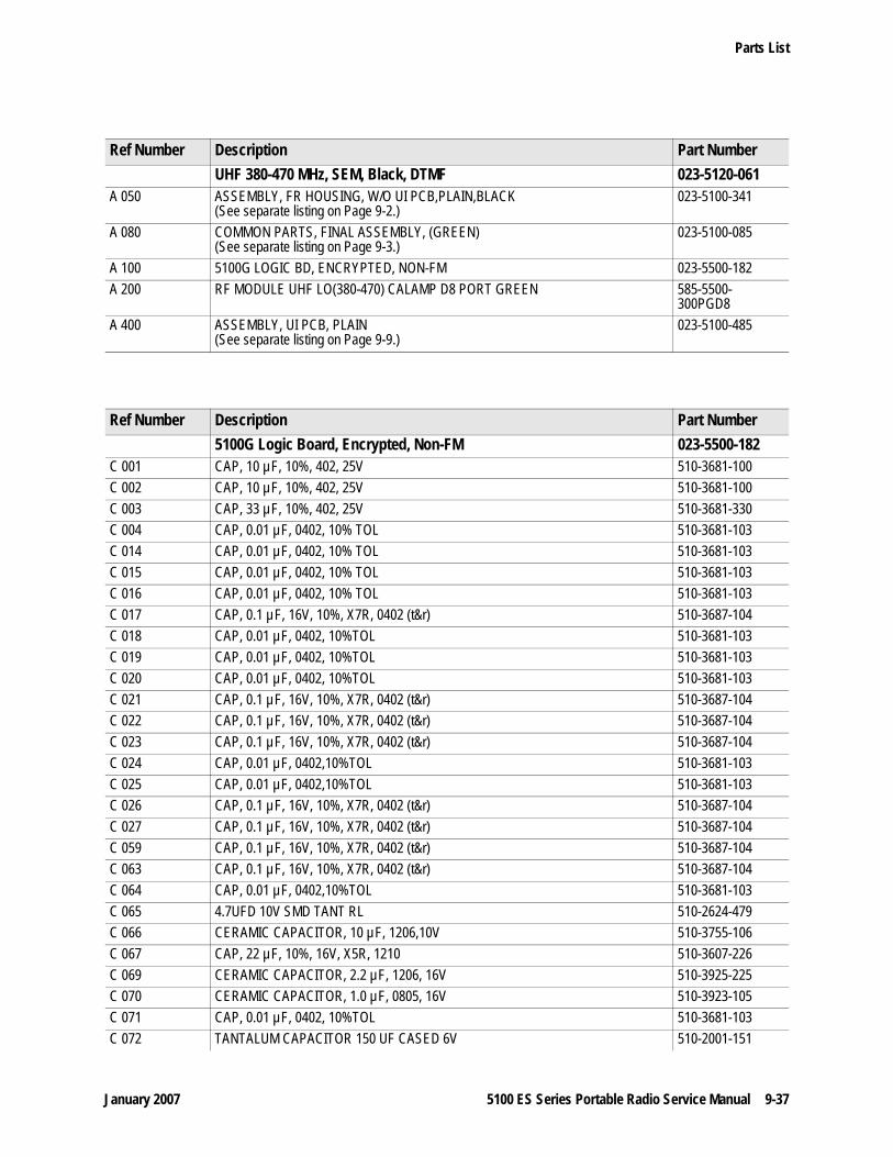
January 2007 5100 ES Series Portable Radio Service Manual 9-37
Parts List
Ref Number Description Part NumberUHF 380-470 MHz, SEM, Black, DTMF 023-5120-061
A 050 ASSEMBLY, FR HOUSING, W/O UI PCB,PLAIN,BLACK(See separate listing on Page 9-2.)
023-5100-341
A 080 COMMON PARTS, FINAL ASSEMBLY, (GREEN)(See separate listing on Page 9-3.)
023-5100-085
A 100 5100G LOGIC BD, ENCRYPTED, NON-FM 023-5500-182A 200 RF MODULE UHF LO(380-470) CALAMP D8 PORT GREEN 585-5500-
300PGD8A 400 ASSEMBLY, UI PCB, PLAIN
(See separate listing on Page 9-9.)023-5100-485
Ref Number Description Part Number5100G Logic Board, Encrypted, Non-FM 023-5500-182
C 001 CAP, 10 µF, 10%, 402, 25V 510-3681-100C 002 CAP, 10 µF, 10%, 402, 25V 510-3681-100C 003 CAP, 33 µF, 10%, 402, 25V 510-3681-330C 004 CAP, 0.01 µF, 0402, 10% TOL 510-3681-103C 014 CAP, 0.01 µF, 0402, 10% TOL 510-3681-103C 015 CAP, 0.01 µF, 0402, 10% TOL 510-3681-103C 016 CAP, 0.01 µF, 0402, 10% TOL 510-3681-103C 017 CAP, 0.1 µF, 16V, 10%, X7R, 0402 (t&r) 510-3687-104C 018 CAP, 0.01 µF, 0402, 10%TOL 510-3681-103C 019 CAP, 0.01 µF, 0402, 10%TOL 510-3681-103C 020 CAP, 0.01 µF, 0402, 10%TOL 510-3681-103C 021 CAP, 0.1 µF, 16V, 10%, X7R, 0402 (t&r) 510-3687-104C 022 CAP, 0.1 µF, 16V, 10%, X7R, 0402 (t&r) 510-3687-104C 023 CAP, 0.1 µF, 16V, 10%, X7R, 0402 (t&r) 510-3687-104C 024 CAP, 0.01 µF, 0402,10%TOL 510-3681-103C 025 CAP, 0.01 µF, 0402,10%TOL 510-3681-103C 026 CAP, 0.1 µF, 16V, 10%, X7R, 0402 (t&r) 510-3687-104C 027 CAP, 0.1 µF, 16V, 10%, X7R, 0402 (t&r) 510-3687-104C 059 CAP, 0.1 µF, 16V, 10%, X7R, 0402 (t&r) 510-3687-104C 063 CAP, 0.1 µF, 16V, 10%, X7R, 0402 (t&r) 510-3687-104C 064 CAP, 0.01 µF, 0402,10%TOL 510-3681-103C 065 4.7UFD 10V SMD TANT RL 510-2624-479C 066 CERAMIC CAPACITOR, 10 µF, 1206,10V 510-3755-106C 067 CAP, 22 µF, 10%, 16V, X5R, 1210 510-3607-226C 069 CERAMIC CAPACITOR, 2.2 µF, 1206, 16V 510-3925-225C 070 CERAMIC CAPACITOR, 1.0 µF, 0805, 16V 510-3923-105C 071 CAP, 0.01 µF, 0402, 10%TOL 510-3681-103C 072 TANTALUM CAPACITOR 150 UF CASED 6V 510-2001-151

9-38 5100 ES Series Portable Radio Service Manual January 2007
Parts List
C 073 TANTALUM CAPACITOR 150 UF CASED 6V 510-2001-151C 076 4.7UFD 10V SMD TANT RL 510-2624-479C 077 CERAMIC CAPACITOR, 10 µF, 1206, 10V 510-3755-106C 078 4.7UFD 10V SMD TANT RL 510-2624-479C 079 CAP, 33 µF, 10%, 402, 25V 510-3681-330C 080 CAP, 33 µF, 10%, 402, 25V 510-3681-330C 081 CAP, 33 µF, 10%, 402, 25V 510-3681-330C 082 CAP, 33 µF, 10%, 402, 25V 510-3681-330C 084 CAP, 33 µF, 10%, 402, 25V 510-3681-330C 085 CAP, 33 µF, 10%, 402, 25V 510-3681-330C 087 CAP, 33 µF, 10%, 402, 25V 510-3681-330C 090 CAP, 0.01 µF, 0402, 10%TOL 510-3681-103C 091 CAP, 22 µF, 10%, 16V, X5R, 1210 510-3607-226C 092 CAP, 0.01 µF, 0402, 10%TOL 510-3681-103C 100 CAP, 0.1 µF, 16V, 10%, X7R, 0402 (t&r) 510-3687-104C 101 CAP, 0.01 µF, 0402, 10%TOL 510-3681-103C 102 4.7UFD 10V SMD TANT RL 510-2624-479C 104 CAP, 0.1 µF, 16V, 10%, X7R, 0402 (t&r) 510-3687-104C 105 CAP, 0.1 µF, 16V, 10%, X7R, 0402 (t&r) 510-3687-104C 109 CAP, 22 µF, 10%, 16V, X5R, 1210 510-3607-226C 110 CAP, 0.01 µF, 0402, 10%TOL 510-3681-103C 111 CAP, 0.01 µF, 0402, 10%TOL 510-3681-103C 114 CAP, 10 µF, 10%, 402, 25V 510-3681-100C 115 CAP, 10 µF, 10%, 402, 25V 510-3681-100C 117 CAP, 0.1 µF, 16V, 10%, X7R, 0402 (t&r) 510-3687-104C 118 CAP, 0.1 µF, 16V, 10%, X7R, 0402 (t&r) 510-3687-104C 119 CAP,0.01 µF, 0402,10%TOL 510-3681-103C 120 CAP,0.01 µF, 0402,10%TOL 510-3681-103C 121 CAP, 0.1 µF, 16V, 10%, X7R, 0402 (t&r) 510-3687-104C 122 CAP, 0.1 µF, 16V, 10%, X7R, 0402 (t&r) 510-3687-104C 123 CERAMIC CAPACITOR, 10 µF, 1206,10V 510-3755-106C 124 CAP, 0.1 µF, 16V, 10%, X7R, 0402 (t&r) 510-3687-104C 125 CAP, 0.1 µF, 16V, 10%, X7R, 0402 (t&r) 510-3687-104C 126 CAP, 0.1 µF, 16V, 10%, X7R, 0402 (t&r) 510-3687-104C 127 CAP, 0.1 µF, 16V, 10%, X7R, 0402 (t&r) 510-3687-104C 128 CAP, 0.1 µF, 16V, 10%, X7R, 0402 (t&r) 510-3687-104C 129 CAP, 0.1 µF, 16V, 10%, X7R, 0402 (t&r) 510-3687-104C 130 CAP, 0.1 µF, 16V, 10%, X7R, 0402 (t&r) 510-3687-104C 132 CAP, 0.01 µF, 0402, 10% TOL 510-3681-103C 133 CAP, 0.01 µF, 0402, 10% TOL 510-3681-103C 134 CAP, 0.1 µF, 16V, 10%, X7R, 0402 (t&r) 510-3687-104C 135 CAP, 220 µF, 16V, 10%, TANT, EIA7343 510-2652-221C 137 CAP, 0.1 µF, 16V, 10%, X7R, 0402 (t&r) 510-3687-104
Ref Number Description Part Number

January 2007 5100 ES Series Portable Radio Service Manual 9-39
Parts List
C 138 CAP, 0.01 µF, 0402, 10% TOL 510-3681-103C 139 CERAMIC CAPACITOR, 1.0 µF, 0805, 16V 510-3923-105C 140 CERAMIC CAPACITOR, 1.0 µF, 0805, 16V 510-3923-105C 141 CERAMIC CAPACITOR, 1.0 µF, 0805, 16V 510-3923-105C 142 CAP, 0.01 µF, 0402, 10% TOL 510-3681-103C 143 CAP, 0.01 µF, 0402, 10% TOL 510-3681-103C 144 CAP, 0.1 µF, 16V, 10%, X7R, 0402 (t&r) 510-3687-104C 145 CAP, 0.1 µF, 16V, 10%, X7R, 0402 (t&r) 510-3687-104C 146 CAP, 0.1 µF, 16V, 10%, X7R, 0402 (t&r) 510-3687-104C 147 CAP, 0.1 µF, 16V, 10%, X7R, 0402 (t&r) 510-3687-104C 148 CAP, 0.1 µF, 16V, 10%, X7R, 0402 (t&r) 510-3687-104C 149 CAP, 0.01 µF, 0402, 10%TOL 510-3681-103C 150 CAP, 0.01 µF, 0402, 10%TOL 510-3681-103C 151 CAP, 470 µF, 10%, 402, 25V 510-3681-471C 152 CAP, 0.1 µF, 16V, 10%, X7R, 0402 (t&r) 510-3687-104C 153 CAP, 0.01 µF, 0402, 10%TOL 510-3681-103C 154 CAP, 0.01 µF, 0402, 10%TOL 510-3681-103C 155 CAP, 0.01 µF, 0402, 10%TOL 510-3681-103C 157 CAP, 0.01 µF, 0402, 10%TOL 510-3681-103C 158 CAP, 0.01 µF, 0402, 10%TOL 510-3681-103C 159 CAP, 0.01 µF, 0402, 10%TOL 510-3681-103C 160 CAP, 0.01 µF, 0402, 10%TOL 510-3681-103
CR 001 DUAL DIODES-COM ANODES 523-1504-024CR 004 SILICON SWITCHING DIODE SC-75 523-1004-021CR 008 DUAL DIODES-COM ANODES 523-1504-024
J 001 CONN, 26-P, ZIF 0.5MM PITCH SMD see notes 515-7111-526J 002 FINE PITCH SMD BD TO BD RECEP 60 PIN (TR) 515-7111-650J 003 SINGLE SPRING CLIP BRIGHT TINNED 75RC-.05-08 537-5001-014J 004 SINGLE SPRING CLIP BRIGHT TINNED 75RC-.05-08 537-5001-014
L 003 10 µH SMT POWER INDUCTOR (SD12-100) 542-9009-100L 004 10 µH SMT POWER INDUCTOR (SD12-100) 542-9009-100L 005 270 nH 0603 SMD INDUCTOR (T&R) 542-9017-274L 007 270 nH 0603 SMD INDUCTOR (T&R) 542-9017-274L 010 270 nH 0603 SMD INDUCTOR (T&R) 542-9017-274L 011 INDUCTOR, 27 UH, 1.2A, SMD, T&R 542-5010-019L 013 270 nH 0603 SMD INDUCTOR (T&R) 542-9017-274L 014 270 nH 0603 SMD INDUCTOR (T&R) 542-9017-274L 015 270 nH 0603 SMD INDUCTOR (T&R) 542-9017-274L 016 10 µH SMT POWER INDUCTOR (SD12-100) 542-9009-100
Ref Number Description Part Number

9-40 5100 ES Series Portable Radio Service Manual January 2007
Parts List
PC 001 PCB, 5100G LOGIC BOARD REV 2 355-5001-8002
Q 001 POWER MOSFET N+P PAIR 20 V SC-70 T&R 576-0006-244Q 002 GEN PURPOSE 3904 BST SC-75 576-0001-029Q 003 POWER MOSFET N+P PAIR 20 V SC-70 T&R 576-0006-244
R 002 RES, 10K, 5%, 402 569-0165-103R 003 RES, 10K, 5%, 402 569-0165-103R 004 RES, 100K, .06W, 5%, 402 569-0165-104R 005 RES, 100K, .06W, 5%, 402 569-0165-104R 009 RES, 0ohm, 5%, 402 569-0165-001R 019 RESISTOR, 1K OHM, 0402, SMT 569-0165-102R 020 RESISTOR, 15K OHM, 0402, SMT 569-0165-153R 022 SURFACE MOUNT 20K,0402, RESISTOR 569-0165-203R 023 RESISTOR, 15K OHM, 0402, SMT 569-0165-153R 024 RESISTOR, 1K OHM, 0402, SMT 569-0165-102R 028 RES, 4.7K, 5%, 402 569-0165-472R 029 RES, 4.7K, 5%, 402 569-0165-472R 030 RES, 10K, 5%, 402 569-0165-103R 031 RES, 30.1K, 1%, 0402 569-0161-447R 032 RES, 30.1K, 1%, 0402 569-0161-447R 033 SURFACE MOUNT 20K,0402, RESISTOR 569-0165-203R 059 RESISTOR 1%, 0402, 100K OHM 569-0161-501R 060 RESISTOR 1%, 0402, 100K OHM 569-0161-501R 061 RESISTOR 1%, 0402, 100K OHM 569-0161-501R 062 RESISTOR 1%, 0402, 100K OHM 569-0161-501R 063 RESISTOR 1%, 0402, 100K OHM 569-0161-501R 064 RES, 100K, .06W, 5%, 402 569-0165-104R 065 RES, 100K, .06W, 5%, 402 569-0165-104R 068 RES, 100K, .06W, 5%, 402 569-0165-104R 069 RES, 100K, .06W, 5%, 402 569-0165-104R 074 CHIP RESISTOR, TAPE & REEL, 0402 569-0165-100R 075 RESISTOR, 100 OHM, 402 SIZE, 5% 569-0165-101R 078 RESISTOR 1%, 221K, 0402 569-0161-534R 081 RESISTOR 1%, 0603, 100K OHM 569-0151-501R 088 RESISTOR, 1K OHM, 0402, SMT 569-0165-102R 090 RESISTOR, 1K OHM, 0402, SMT 569-0165-102R 091 RES, 10K, 5%, 402 569-0165-103R 092 RES, 10K, 5%, 402 569-0165-103R 097 RES, 10K, 5%, 402 569-0165-103R 098 RES, 10K, 5%, 402 569-0165-103R 100 RESISTOR, 1K OHM, 0402,SMT 569-0165-102R 101 RESISTOR, 1K OHM, 0402, SMT 569-0165-102
Ref Number Description Part Number

January 2007 5100 ES Series Portable Radio Service Manual 9-41
Parts List
R 102 RESISTOR, 1K OHM, 0402, SMT 569-0165-102R 103 RESISTOR 1%, 0603, 13K OHM 569-0151-412R 105 RESISTOR, 1K OHM, 0402, SMT 569-0165-102R 106 RESISTOR, 1K OHM, 0402, SMT 569-0165-102R 107 RESISTOR 1%, 0603, 20K OHM 569-0151-430R 110 RESISTOR 1%, 0603, 38.3K OHM 569-0151-457R 111 RESISTOR 1%, 0603, 12.1K OHM 569-0151-409R 182 RES, 10K, 5%, 402 569-0165-103R 186 RES, 10K, 5%, 402 569-0165-103R 188 RES, 10K, 5%, 402 569-0165-103R 190 RES, 10K, 5%, 402 569-0165-103R 191 RES, 10K, 5%, 402 569-0165-103R 193 RES, 10K, 5%, 402 569-0165-103R 194 RES, 10K, 5%, 402 569-0165-103R 195 RES, 10K, 5%, 402 569-0165-103R 236 RESISTOR, 1K OHM,0402, SMT 569-0165-102R 237 RESISTOR, 1K OHM,0402, SMT 569-0165-102R 238 RESISTOR, 1K OHM,0402, SMT 569-0165-102R 239 RESISTOR, 1K OHM,0402, SMT 569-0165-102R 240 RESISTOR, 1K OHM,0402, SMT 569-0165-102R 241 RESISTOR, 1K OHM,0402, SMT 569-0165-102R 242 RESISTOR, 1K OHM,0402, SMT 569-0165-102R 243 RES, 10K, 5%, 402 569-0165-103R 244 RES, 10K, 5%, 402 569-0165-103R 245 RES, 10K, 5%, 402 569-0165-103R 249 RES, 10K, 5%, 402 569-0165-103R 253 RES,100K, .06W, 5%, 402 569-0165-104R 254 RES,100K, .06W, 5%, 402 569-0165-104R 255 CHIP RESISTOR, TAPE & REEL, 0402 569-0165-100R 259 CHIP RESISTOR, TAPE & REEL, 0402 569-0165-100R 260 CHIP RESISTOR, TAPE & REEL, 0402 569-0165-100R 261 CHIP RESISTOR, TAPE & REEL, 0402 569-0165-100R 262 RES, 100K, .06W, 5%, 402 569-0165-104R 263 RES, 100K, .06W, 5%, 402 569-0165-104R 264 RES, 0ohm, 5%, 402 569-0165-001R 265 RESISTOR, 1K OHM, 0402, SMT 569-0165-102R 266 RESISTOR, 1K OHM, 0402, SMT 569-0165-102R 267 RESISTOR, 1K OHM, 0402, SMT 569-0165-102R 268 RESISTOR, 1K OHM, 0402, SMT 569-0165-102R 269 RES, 100K, .06W, 5%, 402 569-0165-104R 270 RES, 100K, .06W,5%, 402 569-0165-104R 271 RES, 100K, .06W, 5%, 402 569-0165-104R 272 RES, 100K, .06W, 5%, 402 569-0165-104
Ref Number Description Part Number
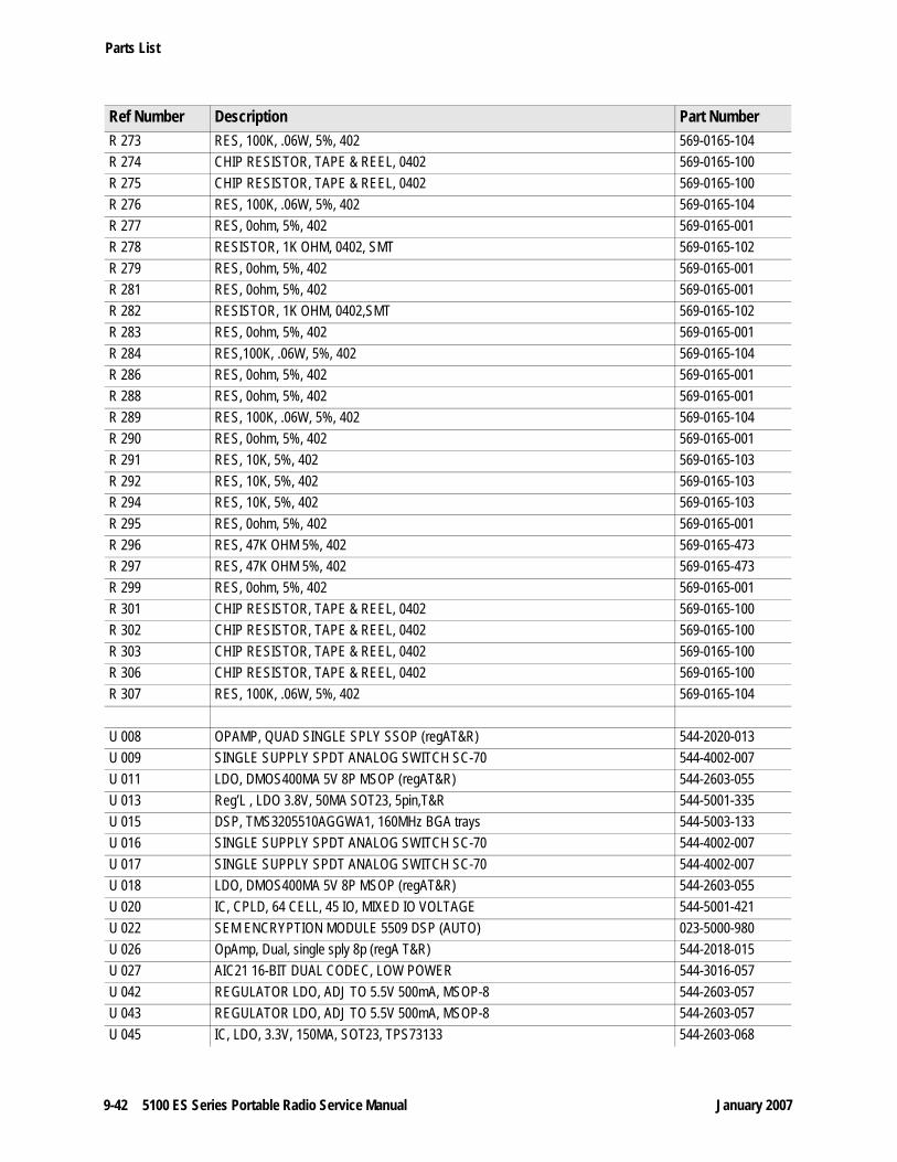
9-42 5100 ES Series Portable Radio Service Manual January 2007
Parts List
R 273 RES, 100K, .06W, 5%, 402 569-0165-104R 274 CHIP RESISTOR, TAPE & REEL, 0402 569-0165-100R 275 CHIP RESISTOR, TAPE & REEL, 0402 569-0165-100R 276 RES, 100K, .06W, 5%, 402 569-0165-104R 277 RES, 0ohm, 5%, 402 569-0165-001R 278 RESISTOR, 1K OHM, 0402, SMT 569-0165-102R 279 RES, 0ohm, 5%, 402 569-0165-001R 281 RES, 0ohm, 5%, 402 569-0165-001R 282 RESISTOR, 1K OHM, 0402,SMT 569-0165-102R 283 RES, 0ohm, 5%, 402 569-0165-001R 284 RES,100K, .06W, 5%, 402 569-0165-104R 286 RES, 0ohm, 5%, 402 569-0165-001R 288 RES, 0ohm, 5%, 402 569-0165-001R 289 RES, 100K, .06W, 5%, 402 569-0165-104R 290 RES, 0ohm, 5%, 402 569-0165-001R 291 RES, 10K, 5%, 402 569-0165-103R 292 RES, 10K, 5%, 402 569-0165-103R 294 RES, 10K, 5%, 402 569-0165-103R 295 RES, 0ohm, 5%, 402 569-0165-001R 296 RES, 47K OHM 5%, 402 569-0165-473R 297 RES, 47K OHM 5%, 402 569-0165-473R 299 RES, 0ohm, 5%, 402 569-0165-001R 301 CHIP RESISTOR, TAPE & REEL, 0402 569-0165-100R 302 CHIP RESISTOR, TAPE & REEL, 0402 569-0165-100R 303 CHIP RESISTOR, TAPE & REEL, 0402 569-0165-100R 306 CHIP RESISTOR, TAPE & REEL, 0402 569-0165-100R 307 RES, 100K, .06W, 5%, 402 569-0165-104
U 008 OPAMP, QUAD SINGLE SPLY SSOP (regAT&R) 544-2020-013U 009 SINGLE SUPPLY SPDT ANALOG SWITCH SC-70 544-4002-007U 011 LDO, DMOS400MA 5V 8P MSOP (regAT&R) 544-2603-055U 013 Reg’L , LDO 3.8V, 50MA SOT23, 5pin,T&R 544-5001-335U 015 DSP, TMS3205510AGGWA1, 160MHz BGA trays 544-5003-133U 016 SINGLE SUPPLY SPDT ANALOG SWITCH SC-70 544-4002-007U 017 SINGLE SUPPLY SPDT ANALOG SWITCH SC-70 544-4002-007U 018 LDO, DMOS400MA 5V 8P MSOP (regAT&R) 544-2603-055U 020 IC, CPLD, 64 CELL, 45 IO, MIXED IO VOLTAGE 544-5001-421U 022 SEM ENCRYPTION MODULE 5509 DSP (AUTO) 023-5000-980U 026 OpAmp, Dual, single sply 8p (regA T&R) 544-2018-015U 027 AIC21 16-BIT DUAL CODEC, LOW POWER 544-3016-057U 042 REGULATOR LDO, ADJ TO 5.5V 500mA, MSOP-8 544-2603-057U 043 REGULATOR LDO, ADJ TO 5.5V 500mA, MSOP-8 544-2603-057U 045 IC, LDO, 3.3V, 150MA, SOT23, TPS73133 544-2603-068
Ref Number Description Part Number
9-43 5100 ES Series Portable Radio Service Manual January 2007
Parts List 5100G Logic Board, Encrypted, Non-FM
U 046 CONV, SYNC STEP DOWN, 2.7-10V IN. 1.8V OUT 544-4006-012U 047 CONV, SYNC STEP DOWN V.REG, 2.7-10V IN, 3.3V OUT 544-4006-014U 049 CONV, SYNC STEP DOWN, 2.7-10V IN. VAR OUT 544-4006-010
Y 001 OSC 20.000 MHz SMD 3.3V -40 / +85C 561-9004-200Y 002 TCXO, 12.288 MHz, 2PPM, HCMOS 518-7012-210
Ref Number Description Part Number

January 2007 5100 ES Series Portable Radio Service Manual 9-44
Parts List
9.2 Exploded Views
Figure 9.1 5100 ES Portable Radio Model III Assembly
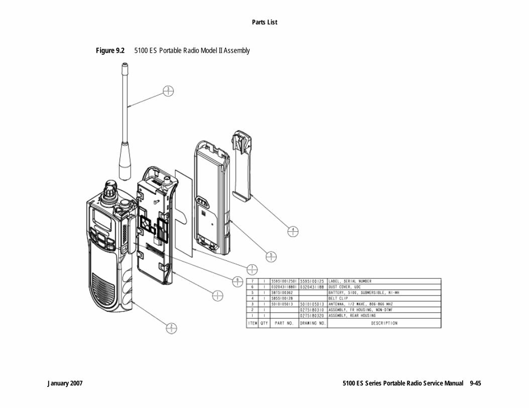
January 2007 5100 ES Series Portable Radio Service Manual 9-45
Parts List
Figure 9.2 5100 ES Portable Radio Model II Assembly

January 2007 5100 ES Series Portable Radio Service Manual 9-46
Parts List
Figure 9.3 5100 ES Portable Radio Model I Assembly

January 2007 5100 ES Series Portable Radio Service Manual 9-47
Parts List
Figure 9.4 Front Housing Assembly Model III

January 2007 5100 ES Series Portable Radio Service Manual 9-48
Parts List
Figure 9.5 Front Housing Assembly Model II

January 2007 5100 ES Series Portable Radio Service Manual 9-49
Parts List
Figure 9.6 Front Housing Assembly Model I

January 2007 5100 ES Series Portable Radio Service Manual 9-50
Parts List
Figure 9.7 Rear Housing Assembly Model I/II/III
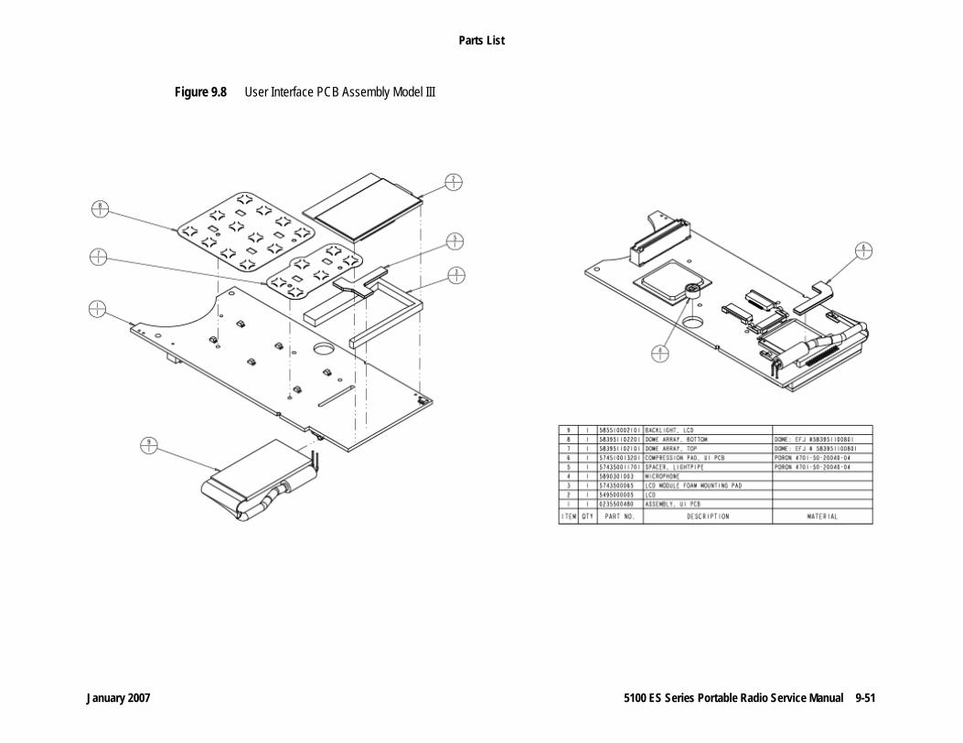
January 2007 5100 ES Series Portable Radio Service Manual 9-51
Parts List
Figure 9.8 User Interface PCB Assembly Model III

January 2007 5100 ES Series Portable Radio Service Manual 9-52
Parts List
Figure 9.9 User Interface PCB Assembly Model II

January 2007 5100 ES Series Portable Radio Service Manual 9-53
Parts List
Figure 9.10 User Interface PCB Assembly Model I

January 2007 5100 ES Series Portable Radio Service Manual 9-54
Parts List
Figure 9.11 Front Cover Assembly Model II/III

January 2007 5100 ES Series Portable Radio Service Manual 9-55
Parts List
Figure 9.12 Front Cover Assembly Model I
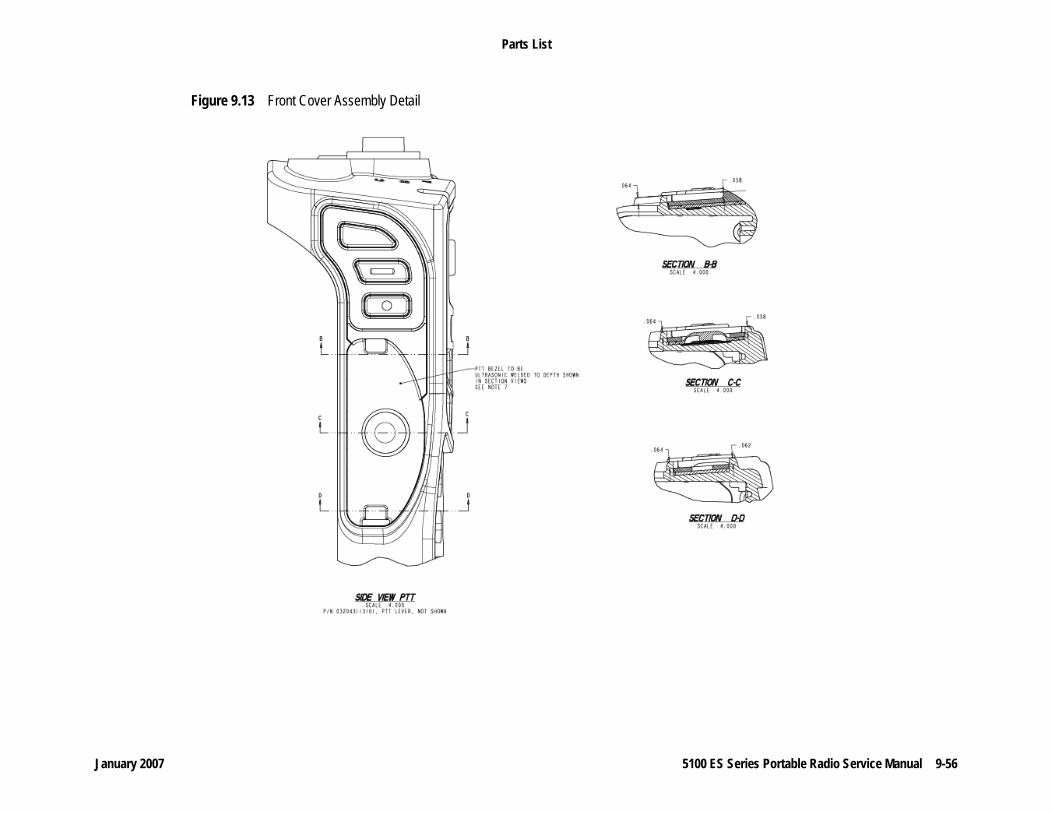
January 2007 5100 ES Series Portable Radio Service Manual 9-56
Parts List
Figure 9.13 Front Cover Assembly Detail
January 2007 5100 ES Series Portable Radio Service Manual 10-1
S E C T I O N
Chapter 10Schematic Diagrams andComponent Layouts
This section contains schematic diagrams and layout illustrations of most components for the 5100 ES Portable Radio.

January 2007 5100 ES Series Portable Radio Service Manual 10-2
Schematic Diagrams and Component Layouts
Figure 10.1 Interconnect Schematic
12
13 12
12
13 12
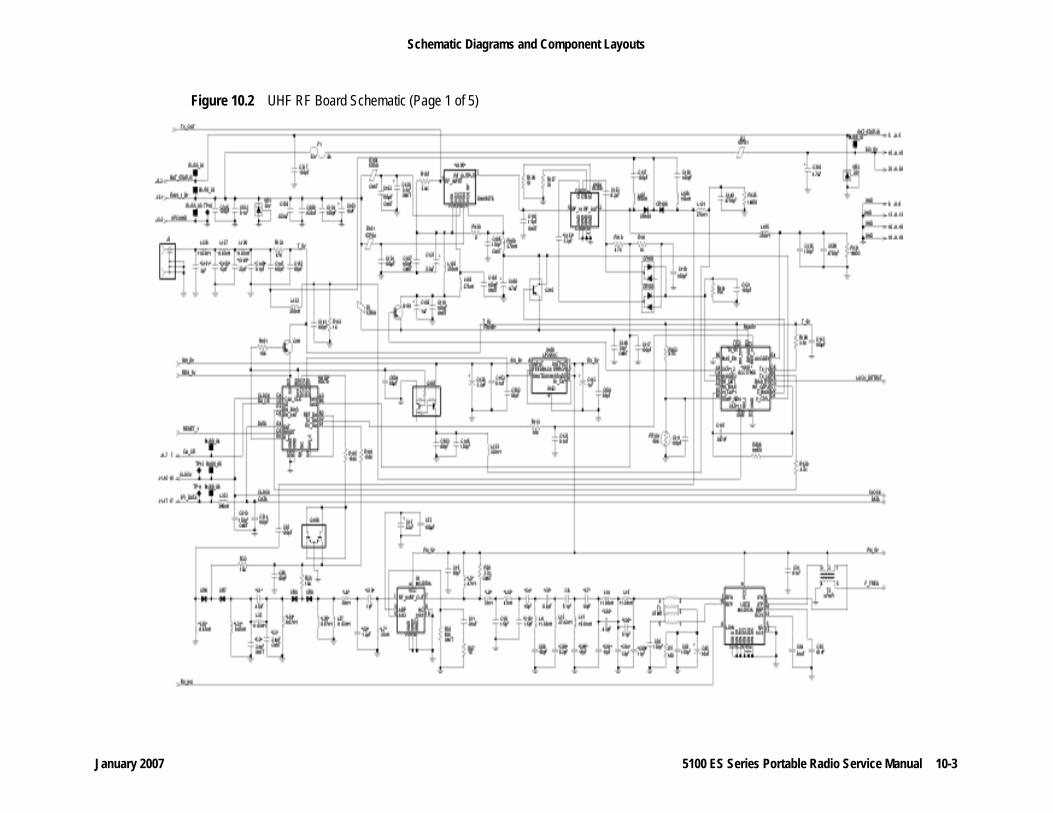
January 2007 5100 ES Series Portable Radio Service Manual 10-3
Schematic Diagrams and Component Layouts
Figure 10.2 UHF RF Board Schematic (Page 1 of 5)

January 2007 5100 ES Series Portable Radio Service Manual 10-4
Schematic Diagrams and Component Layouts
Figure 10.3 UHF RF Board Schematic (Page 2 of 5)

January 2007 5100 ES Series Portable Radio Service Manual 10-5
Schematic Diagrams and Component Layouts
Figure 10.4 UHF RF Board Schematic (Page 3 of 5)
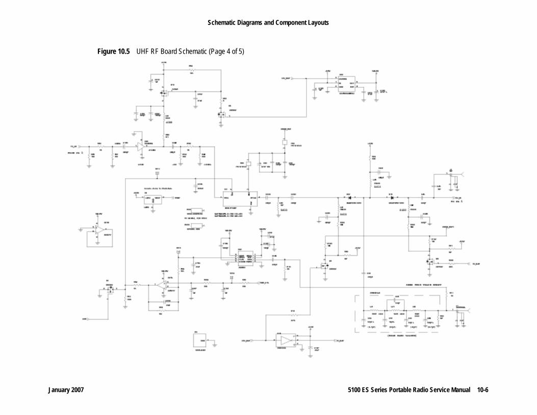
January 2007 5100 ES Series Portable Radio Service Manual 10-6
Schematic Diagrams and Component Layouts
Figure 10.5 UHF RF Board Schematic (Page 4 of 5)

January 2007 5100 ES Series Portable Radio Service Manual 10-7
Schematic Diagrams and Component Layouts
Figure 10.6 UHF RF Board Schematic (Page 5 of 5)

January 2007 5100 ES Series Portable Radio Service Manual 10-8
Schematic Diagrams and Component Layouts
Figure 10.7 UHF RF Board Layout
BOTTOM VIEW
TOP VIEW

January 2007 5100 ES Series Portable Radio Service Manual 10-9
Schematic Diagrams and Component Layouts
Figure 10.8 700/800 MHz RF Board Schematic (Page 1 of 5)
Note Individual replacement parts are not available for the RF board, so the entire board must be replaced if it is defective.
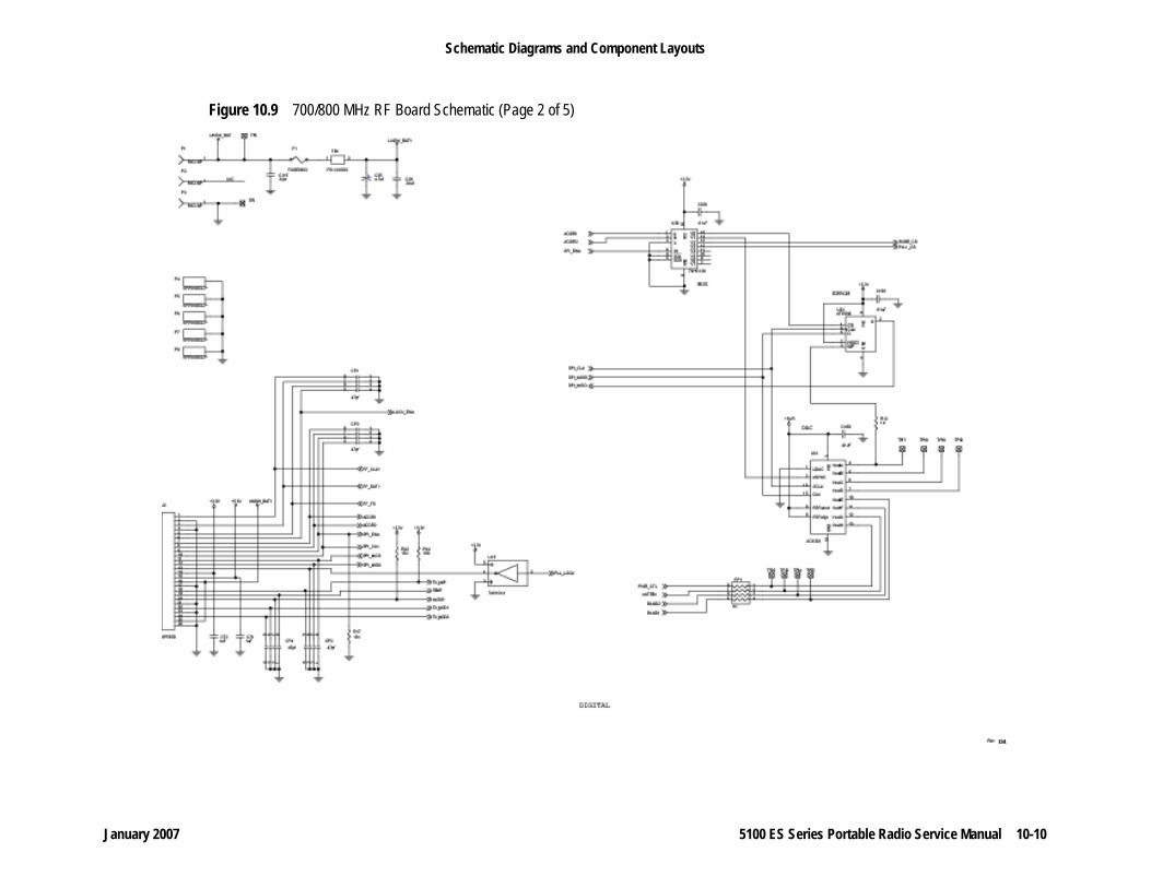
January 2007 5100 ES Series Portable Radio Service Manual 10-10
Schematic Diagrams and Component Layouts
Figure 10.9 700/800 MHz RF Board Schematic (Page 2 of 5)
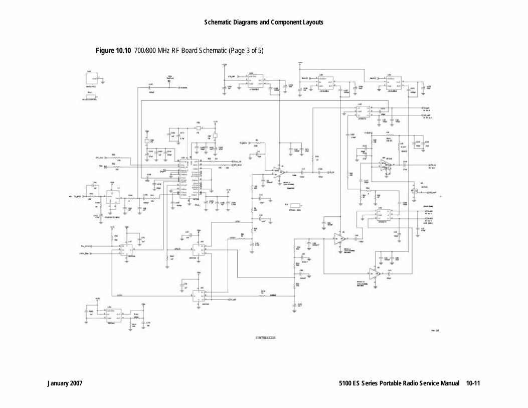
January 2007 5100 ES Series Portable Radio Service Manual 10-11
Schematic Diagrams and Component Layouts
Figure 10.10 700/800 MHz RF Board Schematic (Page 3 of 5)

January 2007 5100 ES Series Portable Radio Service Manual 10-12
Schematic Diagrams and Component Layouts
Figure 10.11 700/800 MHz RF Board Schematic (Page 4 of 5)

January 2007 5100 ES Series Portable Radio Service Manual 10-13
Schematic Diagrams and Component Layouts
Figure 10.12 700/800 MHz RF Board Schematic (Page 5 of 5)

January 2007 5100 ES Series Portable Radio Service Manual 10-14
Schematic Diagrams and Component Layouts
Figure 10.13 700/800 MHz RF Board Layout
Bottom View
Top View

January 2007 5100 ES Series Portable Radio Service Manual 10-15
Schematic Diagrams and Component Layouts
Figure 10.14 023-5500-180/182/185 Logic Board Schematic (Page 1 of 7)
Note The number from 3-11 next to a node label indicates the page number of the circuit to which it connects.
Note Pages 1 and 2 are not used.
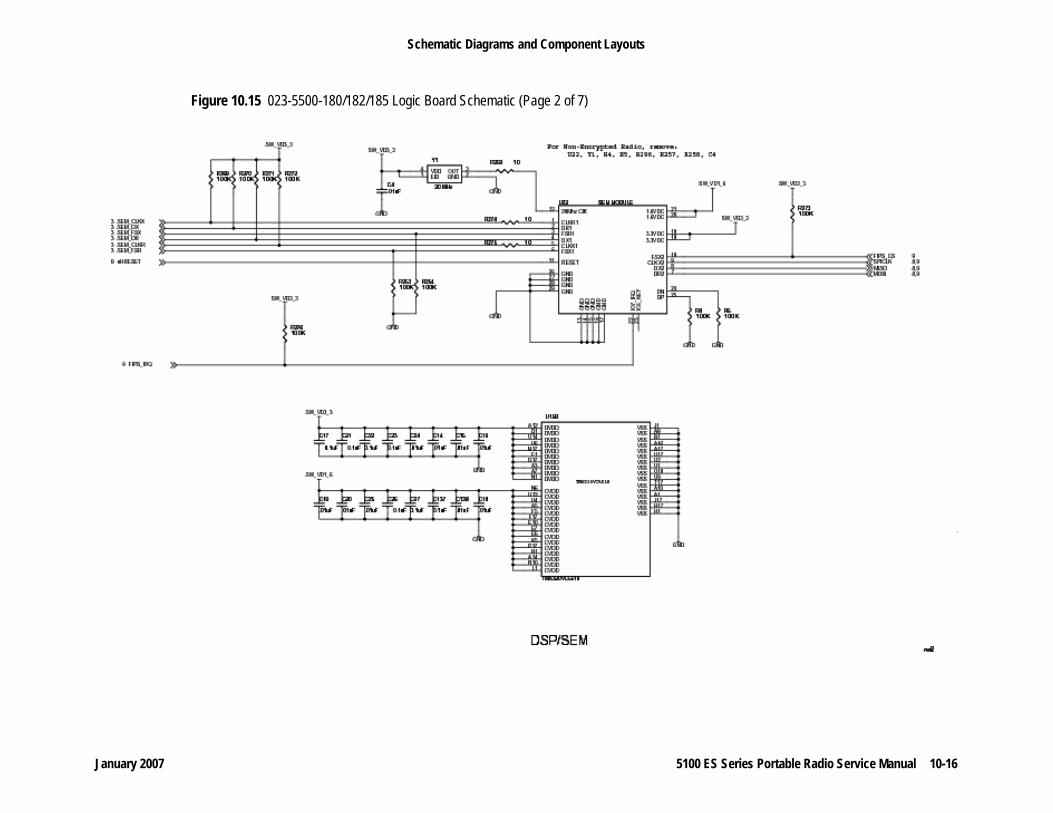
January 2007 5100 ES Series Portable Radio Service Manual 10-16
Schematic Diagrams and Component Layouts
Figure 10.15 023-5500-180/182/185 Logic Board Schematic (Page 2 of 7)

January 2007 5100 ES Series Portable Radio Service Manual 10-17
Schematic Diagrams and Component Layouts
Figure 10.16 023-5500-180/182/185 Logic Board Schematic (Page 3 of 7)

January 2007 5100 ES Series Portable Radio Service Manual 10-18
Schematic Diagrams and Component Layouts
Figure 10.17 023-5500-180/182/185 Logic Board Schematic (Page 4 of 7)

January 2007 5100 ES Series Portable Radio Service Manual 10-19
Schematic Diagrams and Component Layouts
Figure 10.18 023-5500-180/182/185 Logic Board Schematic (Page 5 of 7)
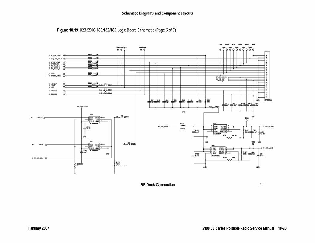
January 2007 5100 ES Series Portable Radio Service Manual 10-20
Schematic Diagrams and Component Layouts
Figure 10.19 023-5500-180/182/185 Logic Board Schematic (Page 6 of 7)
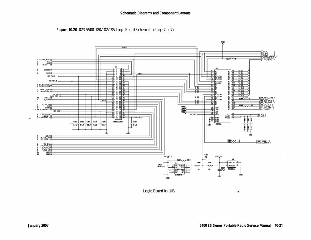
January 2007 5100 ES Series Portable Radio Service Manual 10-21
Schematic Diagrams and Component Layouts
Figure 10.20 023-5500-180/182/185 Logic Board Schematic (Page 7 of 7)

January 2007 5100 ES Series Portable Radio Service Manual 10-22
Schematic Diagrams and Component Layouts
Figure 10.21 023-5500-180/182/185 Logic Board Assembly
Bottom ViewTop View

January 2007 5100 ES Series Portable Radio Service Manual 10-23
Schematic Diagrams and Component Layouts
Figure 10.22 023-5500-480/485 User Interface Board Schematic (Page 1 of 10)
Note The number from 3-12 next to a node label indicates the page number of the circuit to which it connects.
Note Pages 1 and 2 are not used.
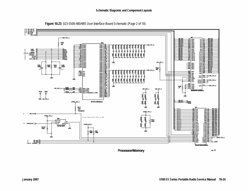
January 2007 5100 ES Series Portable Radio Service Manual 10-24
Schematic Diagrams and Component Layouts
Figure 10.23 023-5500-480/485 User Interface Board Schematic (Page 2 of 10)

January 2007 5100 ES Series Portable Radio Service Manual 10-25
Schematic Diagrams and Component Layouts
Figure 10.24 023-5500-480/485 User Interface Board Schematic (Page 3 of 10)

January 2007 5100 ES Series Portable Radio Service Manual 10-26
Schematic Diagrams and Component Layouts
Figure 10.25 023-5500-480/485 User Interface Board Schematic (Page 4 of 10)
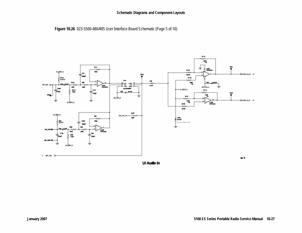
January 2007 5100 ES Series Portable Radio Service Manual 10-27
Schematic Diagrams and Component Layouts
Figure 10.26 023-5500-480/485 User Interface Board Schematic (Page 5 of 10)

January 2007 5100 ES Series Portable Radio Service Manual 10-28
Schematic Diagrams and Component Layouts
Figure 10.27 023-5500-480/485 User Interface Board Schematic (Page 6 of 10)
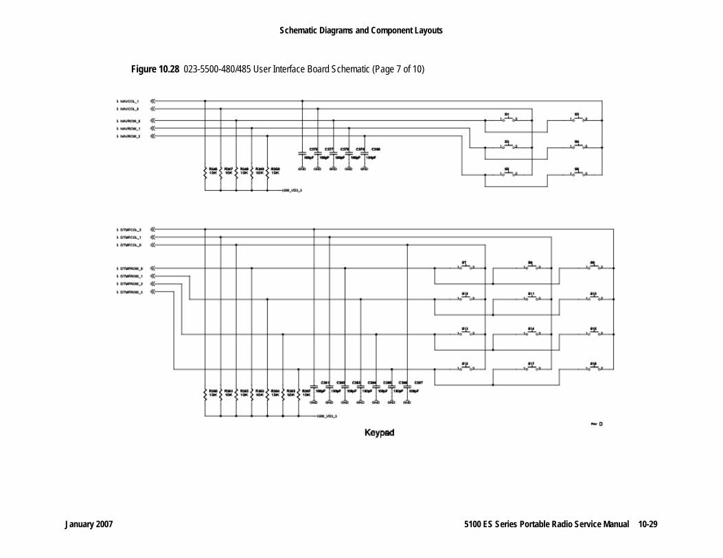
January 2007 5100 ES Series Portable Radio Service Manual 10-29
Schematic Diagrams and Component Layouts
Figure 10.28 023-5500-480/485 User Interface Board Schematic (Page 7 of 10)

January 2007 5100 ES Series Portable Radio Service Manual 10-30
Schematic Diagrams and Component Layouts
Figure 10.29 023-5500-480/485 User Interface Board Schematic (Page 8 of 10)

January 2007 5100 ES Series Portable Radio Service Manual 10-31
Schematic Diagrams and Component Layouts
Figure 10.30 023-5500-480/485 User Interface Board Schematic (Page 9 of 10)
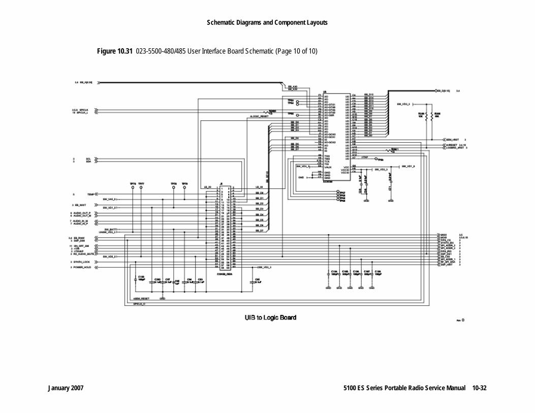
January 2007 5100 ES Series Portable Radio Service Manual 10-32
Schematic Diagrams and Component Layouts
Figure 10.31 023-5500-480/485 User Interface Board Schematic (Page 10 of 10)

January 2007 5100 ES Series Portable Radio Service Manual 10-33
Schematic Diagrams and Component Layouts
Figure 10.32 023-5500-480/485 User Interface Board Assembly
Top View
Bottom View

January 2007 5100 ES Series Portable Radio Service Manual 10-34
Schematic Diagrams and Component Layouts
Figure 10.33 023-5500-480-01/487 User Interface Board Schematic (Page 1 of 10)
Note The number from 3-12 next to a node label indicates the page number of the circuit to which it connects.
Note Pages 1 and 2 are not used.

January 2007 5100 ES Series Portable Radio Service Manual 10-35
Schematic Diagrams and Component Layouts
Figure 10.34 023-5500-480-01/487 User Interface Board Schematic (Page 2 of 10)

January 2007 5100 ES Series Portable Radio Service Manual 10-36
Schematic Diagrams and Component Layouts
Figure 10.35 023-5500-480-01/487 User Interface Board Schematic (Page 3 of 10)
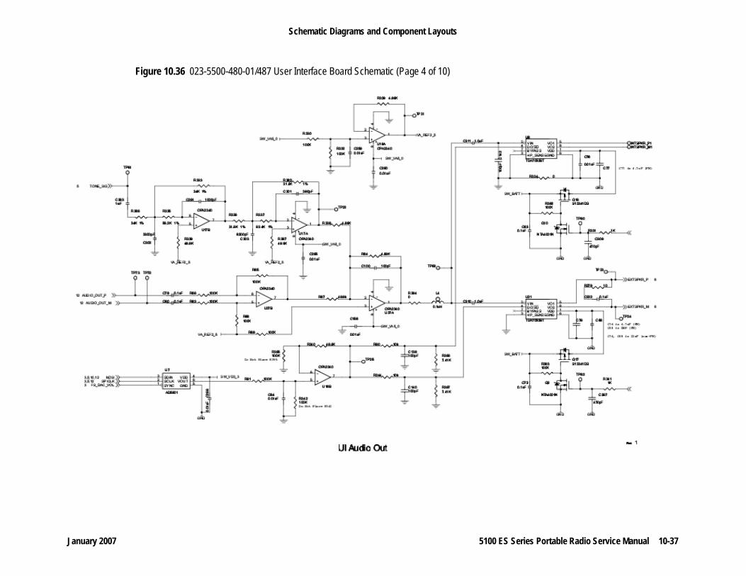
January 2007 5100 ES Series Portable Radio Service Manual 10-37
Schematic Diagrams and Component Layouts
Figure 10.36 023-5500-480-01/487 User Interface Board Schematic (Page 4 of 10)

January 2007 5100 ES Series Portable Radio Service Manual 10-38
Schematic Diagrams and Component Layouts
Figure 10.37 023-5500-480-01/487 User Interface Board Schematic (Page 5 of 10)

January 2007 5100 ES Series Portable Radio Service Manual 10-39
Schematic Diagrams and Component Layouts
Figure 10.38 023-5500-480-01/487 User Interface Board Schematic (Page 6 of 10)

January 2007 5100 ES Series Portable Radio Service Manual 10-40
Schematic Diagrams and Component Layouts
Figure 10.39 023-5500-480-01/487 User Interface Board Schematic (Page 7 of 10)

January 2007 5100 ES Series Portable Radio Service Manual 10-41
Schematic Diagrams and Component Layouts
Figure 10.40 023-5500-480-01/487 User Interface Board Schematic (Page 8 of 10)

January 2007 5100 ES Series Portable Radio Service Manual 10-42
Schematic Diagrams and Component Layouts
Figure 10.41 023-5500-480-01/487 User Interface Board Schematic (Page 9 of 10)
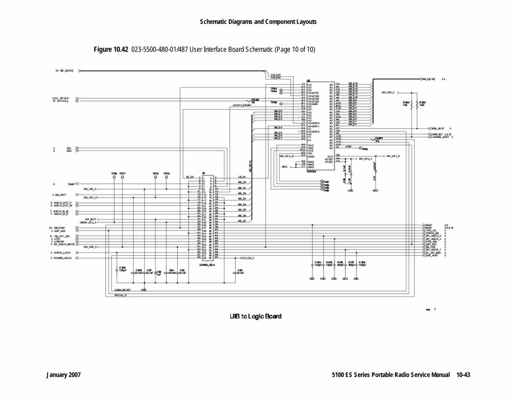
January 2007 5100 ES Series Portable Radio Service Manual 10-43
Schematic Diagrams and Component Layouts
Figure 10.42 023-5500-480-01/487 User Interface Board Schematic (Page 10 of 10)

January 2007 5100 ES Series Portable Radio Service Manual 10-44
Schematic Diagrams and Component Layouts
Figure 10.43 023-5500-480-01/487 User Interface Board Assembly
Top View
Bottom View

January 2007 5100 ES Series Portable Radio Service Manual 10-45
Schematic Diagrams and Component Layouts
Figure 10.44 Cable Schematics
15
9 6
12
12 13
UDC Pin Numbering
DB9 F Pin Numbering
Programming Cable SchematicPart No. 023-5100-920
Test Cable SchematicPart No. 023-5100-940

10-46 5100 ES Series Portable Radio Service Manual January 2007
Schematic Diagrams and Component Layouts