50PS60 Plasma Display - Diagramas...
142
Advanced Single Scan Troubleshooting Training Manual 50PS60 Plasma Display 50PS60 Plasma Display July 2009
Transcript of 50PS60 Plasma Display - Diagramas...

Advanced Single Scan Troubleshooting
Training Manual
50PS60 Plasma Display50PS60 Plasma Display
July 2009

TOPICS PRELIMINARY ........................................ 2 Outline .......................................................... 2 Overview ...................................................... 3 Safety Notice and Cautions .......................... 4 ESD Notice .................................................. 5 Regulatory Info. ............................................ 5 Contact Information ..................................... 6 Handling and Safety ..................................... 7 Basic Troubleshooting Steps ........................ 8 PRODUCT INFORMATION ................... 9 Feature List .................................................. 10 Product Logos .............................................. 12 600Hz Sub Field Driving ............................. 15 Remote Control ............................................ 17 Accessing Service Menu .............................. 18 Rear and Side Inputs .................................... 19 Software Download Screen .......................... 20 Dimensions .................................................. 21 DISASSEMBLY ......................................... 22 Back Cover Removal ................................... 23 Circuit Board Layout ................................... 24 Power supply board Removal ...................... 25 Main board Removal .................................... 26 Control board Removal ................................ 27
50PS60 TABLE OF CONTENTS
TOPICS DISASSEMBLY continued Y-SUS board Removal ................................. 28 Top Y-Drive board Removal ........................ 29 Bottom Y-Drive board .................................. 30 Z-SUS board Removal ................................. 31 Ft Control board Removal ............................ 32 X-Board Removal Text ................................ 33 X-Board Removal ......................................... 34 TROUBLESHOOTING ............................. 35 Signal and Voltage Block Diagram .............. 36 Panel Label Explained .................................. 37 Adjustment Order **Important** ................. 38 Power Supply ............................................... 39 Y-Sustain ...................................................... 51 Y-drive Upper and Lower ............................. 67 Z-SUS board ................................................. 77 Control board ................................................ 84 X-Drive boards ............................................. 99 Main (Digital) board ..................................... 112 Ft Control (IR) .............................................. 129 Side Key ....................................................... 137 11 X 17 Foldout Section ............................. 139
Page 1

2 Fall 2009 1080P Plasma 50PS60
Overview of Topics to be Discussed
• Y SUS Board
• Z SUS Output Board (Connects directly with FPC to Panel)• Y Drive Boards
• Control Board• X Drive Boards (3)
Circuit Board Operation, Troubleshooting and Alignment of :• Switch Mode Power Supply
• Main Board
Section 1
Section 2
Contact Information, Preliminary Matters, Specifications,Plasma Overview, General Troubleshooting Steps, Disassembly Instructions, Voltage and Signal Distribution
OUTLINEOUTLINE
• Power Button (Front Key Board)NEW
Receives its 5V from Power Supply, not Y-SUS
Turns off the SMPS via Key On line.
NEW

3 Fall 2009 1080P Plasma 50PS60
50PS60 Plasma DisplaySection 1
This Section will cover Contact Information and remind the Technician of Important Safety Precautions for the Customers Safety as well as the Technician and the Equipment.
Basic Troubleshooting Techniques which can save time and money sometimes can be overlooked. These techniques will also be presented.
This Section will get the Technician familiar with the Disassembly, Identification and Layout of the Plasma Display Panel.
At the end of this Section the Technician should be able to Identify the Circuit Boards and have the ability and knowledge necessary to safely remove and replace any Circuit Board or Assembly.
Overview of Topics to be DiscussedOverview of Topics to be Discussed

4 Fall 2009 1080P Plasma 50PS60
IMPORTANT SAFETY NOTICEIMPORTANT SAFETY NOTICE
The information in this training manual is intended for use by persons possessing an adequate background in electrical equipment, electronic devices, and mechanical systems. In any attempt to repair a major Product, personal injury and property damage can result. The manufacturer or seller maintains no liability for the interpretation of this information, nor can it assume any liability in conjunction with its use. When servicing this product, under no circumstances should the original design be modified or altered without permission from LG Electronics. Unauthorized modifications will not only void the warranty, but may lead to property damage or user injury. If wires, screws, clips, straps, nuts, or washers used to complete a ground path are removed for service, they must be returned to their original positions and properly fastened.
CAUTIONCAUTION
To avoid personal injury, disconnect the power before servicing this product. If electrical power is required for diagnosis or test purposes, disconnect the power immediately after performing the necessary checks. Also be aware that many household products present a weight hazard. At least two people should be involved in the installation or servicing of such devices. Failure to consider the weight of an product could result in physical injury.
Preliminary Matters (The Fine Print)Preliminary Matters (The Fine Print)
5 Fall 2009 1080P Plasma 50PS60
Today’s sophisticated electronics are electrostatic discharge (ESD) sensitive. ESD can weaken or damage the electronics in a manner that renders them inoperative or reduces the time until their next failure. Connect an ESD wrist strap to a ground connection point or unpainted metal in the product. Alternatively, you can touch your finger repeatedly to a ground connection point or unpainted metal in the product. Before removing a replacement part from its package, touch the anti-static bag to a ground connection point or unpainted metal in the product. Handle the electronic control assembly by its edges only. When repackaging a failed electronic control assembly in an anti-static bag, observe these same precautions.
REGULATORY INFORMATIONREGULATORY INFORMATION
This equipment has been tested and found to comply with the limits for a Class B digital device, pursuant to Part 15 of the FCC Rules. These limits are designed to provide reasonable protection against harmful interference when the equipment is operated in a residential installation. This equipment generates, uses, and can radiate radio frequency energy, and, if not installed and used in accordance with the instruction manual, may cause harmful interference to radio communications. However, there is no guarantee that interference will not occur in a particular installation. If this equipment does cause harmful interference to radio or television reception, which can be determined by turning the equipment off and on, the user is encouraged to try to correct the interference by one or more of the following measures: Reorient or relocate the receiving antenna; Increase the separation between the equipment and the receiver; Connect the equipment to an outlet on a different circuit than that to which the receiver is connected; or consult the dealer or an experienced radio/TV technician for help.
ESD NOTICEESD NOTICE (Electrostatic Static Discharge)(Electrostatic Static Discharge)

6 Fall 2009 1080P Plasma 50PS60
Also available on the Also available on the Plasma pagePlasma page
New Training Materials on New Training Materials on the Learning Academy sitethe Learning Academy site
6
CONTACT INFORMATIONCONTACT INFORMATIONCustomer Service (and Part Sales) (800) 243-0000
Technical Support (and Part Sales) (800) 847-7597
USA Website (GCSC) aic.lgservice.com
Customer Service Website us.lgservice.com
LG Web Training lge.webex.com
LG CS Academy lgcsacademy.com
LG Electronics Alabama, Inc. 201 James Record Road, Huntsville,
AL, 35813.
http://136.166.4.200
Published August 2009 by LG Technical Support and Training
32LG40, 32LH30, 42LG60, 42LG70, 42LH20, 42LH40, 42LH50, 47LG9042PG20, 42PQ20, 42PQ30, 50PG20, 50PS80, 50PS60
LCD-DV:PLASMA:
Plasma PanelAlignment Handbook

7 Fall 2009 1080P Plasma 50PS60
Safety & Handling Regulations
1. Check the appearance of the Replacement Panel and Circuit Boards for both physical damage and part number accuracy.
2. Check the model label. Verify model names and board model matches.
3. Check details of defective condition and history. Example: Y Board Failure, Mal-discharge on screen, etc.
1. Approximately 10 minute pre-run time is required before any adjustments are performed.
2. Refer to the Voltage Sticker inside the Panel when making adjustments on the Power Supply, Y SUS and Z SUS Boards.
Always adjust to the specified voltage level.
3. Be cautious of electric shock from the PDP module since the PDP module uses high voltage, check that the Power Supply
and Drive Circuits are completely discharged because of residual current stored before Circuit Board removal.
4. C-MOS circuits are used extensively for processing the Drive Signals and should be protected from static electricity.
5. The PDP Module must be carried by two people. Always carry vertical NOT horizontal.
6. The Plasma television should be transported vertical NOT horizontal.
7. Exercise care when making voltage and waveform checks to prevent costly short circuits from damaging the unit.
8. Be cautious of lost screws and other metal objects to prevent a possible short in the circuitry.
9. New Panels and Frames are much thinner than previous models. Be Careful with flexing these panels. Be careful with lifting Panels from a horizontal position. Damage to the Frame mounts or panel can occur.
10. New Plasma models have much thinner cabinet assemblies and mounts. Be extremely careful when moving the set around as damage can occur.
Checking Points to be Considered
SECTION 1: SECTION 1: PLASMA OVERVIEWPLASMA OVERVIEW

8 Fall 2009 1080P Plasma 50PS60
Basic Troubleshooting StepsBasic Troubleshooting Steps
Define, Localize, Isolate and Correct
•Define Look at the symptom carefully and determine what circuits could be causing the failure. Use your senses Sight, Smell, Touch and Hearing. Look for burned parts and check for possible overheated components. Capacitors will sometimes leak dielectric material and give off a distinct odor. Frequency of power supplies will change with the load, or listen for relay closing etc. Observation of the front Power LED may give some clues.
•Localize After carefully checking the symptom and determining the circuits to be checked and after giving a thorough examination using your senses the first check should always be the DC Supply Voltages to those circuits under test. Always confirm the supplies are not only the proper level but be sure they are noise free. If the supplies are missing check the resistance for possible short circuits.
•Isolate To further isolate the failure, check for the proper waveforms with the Oscilloscope to make a final determination of the failure. Look for correct Amplitude Phasing and Timing of the signals also check for the proper Duty Cycle of the signals. Sometimes “glitches” or “road bumps” will be an indication of an imminent failure.
•Correct The final step is to correct the problem. Be careful of ESD and make sure to check the DC Supplies for proper levels. Make all necessary adjustments and lastly always perform a Safety AC Leakage Test before returning the product back to the Customer.

9 Fall 2009 1080P Plasma 50PS60
This section of the manual will discuss the specifications of the 50PS60 Single layer design. The 1080p Full HD resolution and THXDisplay certification makes this series the must have HDTV in 2009.
Product InformationProduct Information

10 Fall 2009 1080P Plasma 50PS60
Specifications Pg 1Specifications Pg 1 1080P PLASMA HDTVFull HD 1080p Plasma TV (50” diagonal)
•50" Screen •Full HD 1080p •THX Display Certification and THX Cinema Mode •THX Media Director •Super Bright Panel: 1,500 cd/m2 Brightness•30,000:1 Contrast Ration•600Hz Sub Field Driving•Four (4) HDMI (V.1.3 with Deep Color) •ISFccc ready •USB 2.0 for access to digital music and photos (MP3, JPEG) •LG SimpLink(TM) Connectivity •Smart Energy Saving •LG Core Technologies:
(Clear Voice II, Invisible Speaker, Picture Wizard, Intelligent Sensor)•Easy UI menu interface •Pure Black Level •Auto Navigation:
(VCR, DVD, Bluray, HD DVD, SetTop Box, Satellite, Cable Box, Game, PC)•Input Labeling

11 Fall 2009 1080P Plasma 50PS60
Specifications Pg 2Specifications Pg 2 (Continued from Previous Page)
•Quick View (Previous Channel) •Parental Control w/V-Chip •Key Lock •Closed Caption 3 (English, Spanish, French) •Trilingual Menus (English/Spanish/French) •EZ Menus (High Performance Interface) •Channel Add/Delete •Favorite Channel •Auto Clock •Manual Clock •On/Off Timer •Sleep Timer •SimpLink™•Auto Off (When no video is present) •Image Sticking Minimization•100,000 Hour Panel Life (typical)•NTSC/ATSC Tuners with Clear QAM

12 Fall 2009 1080P Plasma 50PS60
Specifications Logo Familiarization (Pixels, HDMI, Invisible SpeSpecifications Logo Familiarization (Pixels, HDMI, Invisible Speakers, XD Engine)akers, XD Engine)
Invisible SpeakerPersonally tuned by Mr. Mark Levinson for LG TAKE IT TO THE EDGE newly introduces ‘Invisible Speaker’ system, guaranteeing first class audio quality personally tuned by Mr. Mark Levinson, world renowned as an audio authority. It provides Full Sweet Spot and realistic sound equal to that of theaters with its Invisible Speaker.
FULL HD RESOLUTION 1080p HD Resolution Pixels: 1920 (H) × 1080 (V)High definition television is the highest performance segment of the DTV system used in the US. It’s a wide screen, high-resolution video image, coupled with multi-channel, compact-disc quality sound.
HDMI (1.3 Deep Color) Digital multi-connectivity HDMI (1.3 Deep color) provides a wider bandwidth (340MHz, 10.2Gbps) than that of HDMI 1.2, delivering a broader range of colors, and also drastically improves the data-transmission speed.
Dual XD EngineRealizing optimal quality for all imagesOne XD Engine optimizes the images from RF signals as another XDEngine optimizes them from External inputs. Dual XD Engine presents images with optimal quality two times higher than those of previous models.

13 Fall 2009 1080P Plasma 50PS60
Specifications Logo Familiarization (Picture Wizard)Specifications Logo Familiarization (Picture Wizard)
Customers can customize picture performance without the need for additional expense.
Picture Wizard easily guides consumers through the calibration process using on-screen reference points.

14 Fall 2009 1080P Plasma 50PS60
Specifications Logo Familiarization (AV Model, Specifications Logo Familiarization (AV Model, VolVol Control, Clear Voice, Energy)Control, Clear Voice, Energy)
AV Mode "One click" - Cinema, Sports, Game mode.TAKE IT TO THE EDGE is a true multimedia TV with an AV Mode which allows you to choose from 3 different modes of Cinema, Sports and Game by a single click of a remote control.
Clear Voice Clearer dialogue sound Enhanced “Clear Voice” feature with 12 level voice control (-6 to +6) enables adjustment to the voice frequency ensuring clear sound despite loud backgroundnoise.
Save Energy, Save MoneyHome electronic products use energy when they're off to power features like clock displays and remote controls. Those that have earned the ENERGY STAR use as much as 60% less energy to perform these functions, while providing the same performance at the same price as less-efficient models. Less energy means you pay less on your energy bill. Draws less than 1 Watt in stand by.
Save Energy, Save MoneyIt reduces the plasma display’s power consumption.The default factory setting complies with the Energy Star requirements and is adjusted to the comfortable level to be viewed at home.(Turns on Intelligent Sensor).
Cinema Mode isPre-calibratedusing ISFccc,(new in 2009)

15 Fall 2009 1080P Plasma 50PS60
(600 Hz Sub Field Driving)
• 600 Hz Sub Field Driving is achieved by using 10 sub-fields per frame process (vs. Comp. 8 sub-field/frame)
• No smeared images during fast motion scenes
600Hz Sub Field Driving600Hz Sub Field Driving
Note: Sub field 2 Note: Sub field 2 through 10 are through 10 are
actually in reverse. actually in reverse. Brighter image Brighter image should be last.should be last.
Sub Field firing occurs using wall charge and polarity differences between Y-SUS and Z-SUS signals.

16 Fall 2009 1080P Plasma 50PS60
Dazzling ‘visual and sound’ performance (certified by THX)
• LG is one of the first consumer electronics companies to achieve THX Display Certification. An industry benchmark for video quality, THX Display Certification signifies that an HDTV delivers exceptional images, bringing more immersive movie, broadcast and video game experiences to your living room.
• Long history in the video category• DVD/D-cinema mastering programs, THX Optimizer• THX is unique, since it is involved in every step of the production chain• Mission : make the picture at home look like the picture in the studio
THX Familiarization THX Familiarization

17 Fall 2009 1080P Plasma 50PS60
Remote ControlRemote Control
TOP PORTIONBOTTOM PORTION

18 Fall 2009 1080P Plasma 50PS60
Accessing the Service MenuAccessing the Service Menu
REMOTETOP PORTION
SIDE KEYS
To access the Service Menu.1) Turn the Set On2) Simultaneously, Press and
“Hold” the Menu Key on the Side Key pad and Press and “Hold” the Menu Key on the Remote approximately 5 seconds.
3) If Customer’s Menu appears, continue to hold until it disappears.
4) The Service Menu appears
Note: It is possible, dependant upon the Software Version, a Password may be required to enter the Service Menu.
If a password is required, enter0000
19 Fall 2009 1080P Plasma 50PS60
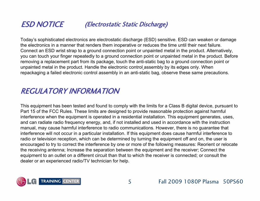
Rear and Side Input JacksRear and Side Input Jacks
USBMusic/Pictures andSoftware Upgrades
20 Fall 2009 1080P Plasma 50PS60
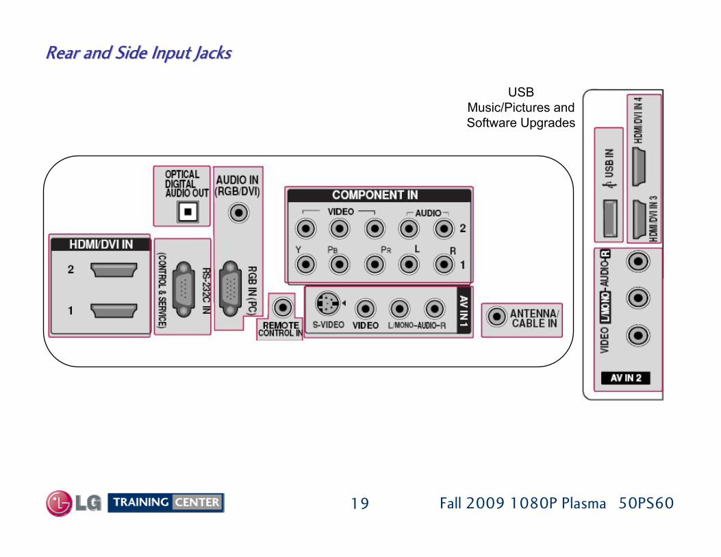
USB Download1) Open the USB Flash Drive.
5) Cursor left and highlight ‘START’ Button and push ‘Enter’ button using the remote control.
6) You can see the download progress Bar.
7) Do not unplug until unit has automatically restarted.
8) When download is completed,
you will see “COMPLETE”.
9) Your TV will be restarted automatically.
※CAUTION:
Do not remove AC power or the USB Flash Drive.Do not turn off Power, during the upgrade process.
2) Copy new software (xxx.bin) to Root.Make sure to have correct software file.
3) With TV turned on, insert USB flash drive.
4) You can see the message “TV Software Upgrade”
Shows theCurrently Installed
Version
Shows theSoftware Versionfound on the USB
Flash Drive
Shows theSoftware file
found on the USBFlash Drive

3-1/8"78.7mm
13-7/8"353mm
1-3/4"45mm
50PS60 Dimensions
30-3/8"772mm
48-5/16"1226.8mm
Remove 4 screws to remove stand for
wall mount
Model No.Serial No.
Label
15-5/16"405mm
25-7/16"646mm
32-1/2"825.5mm
5-11/16"145mm
6-7/8"174mm
2-1/8"54mm
15-3/4"400mm
4-3/4"120mm
15-3/4"400mm
15-3/4"400mm
15-3/4"400mm
80 lbs with Stand74.5 lbs without StandWeight:
21
There must be at least 4 inches of Clearance on all sides295W (Typical)0.13W (Stand-By)
Power:

22 Fall 2009 1080P Plasma 50PS60
This section of the manual will discuss Disassembly, Layout and Circuit Board Identification, of the 50PS60 Advanced Single Scan Plasma Display Panel.
Upon completion of this section the Technician will have a betterunderstanding of the disassembly procedures, the layout of the printedcircuit boards and be able to identify each board.
DISASSEMBLY SECTIONDISASSEMBLY SECTION

Removing the Back CoverRemoving the Back Cover
To remove the back cover, remove the 29 screwsIndicated by the arrows.
(The Stand does not need to be removed).
PAY CLOSE ATTENTION TO THE TYPE, SIZE AND LENGTHOf the screws when replacing the back cover.
Improper type can damage the front.
23

24 Fall 2009 1080P Plasma 50PS60
Circuit Board LayoutCircuit Board Layout
Y SUS PWB
Z-SUS PWB
Right “X”Left “X”
Main PWB
Power Supply(SMPS) PWB
FPC
FPC
PowerButton
FPCFPC
AC In
Side Input(part of main)
FPCFPC
FPCFPC
FPCFPC
FPC
Center “X”
Z-SUBPWB
Y Drive Upper
Panel Voltage Label
Control PWB
Panel ID Label
Conductive Tape Under Main PWB
TCPHeat SinkControl Keys
Y Drive Lower
Invisible Speakers

25 Fall 2009 1080P Plasma 50PS60
SMPS (Switch Mode Power Supply) PWB RemovalSMPS (Switch Mode Power Supply) PWB Removal
P812P811
P813
SC101
Disconnect P811, P812, P813 and SC101Then Remove the 8 Screws

26 Fall 2009 1080P Plasma 50PS60
Main PWB RemovalMain PWB Removal
P1001
Disconnect P1001, P1005 and P1006
Disconnect P1003 by lifting up the locking mechanism and removing the LVDS ribbon cable.
Then Remove the 4 Screws
P1005
P1006
P1003
27 Fall 2009 1080P Plasma 50PS60
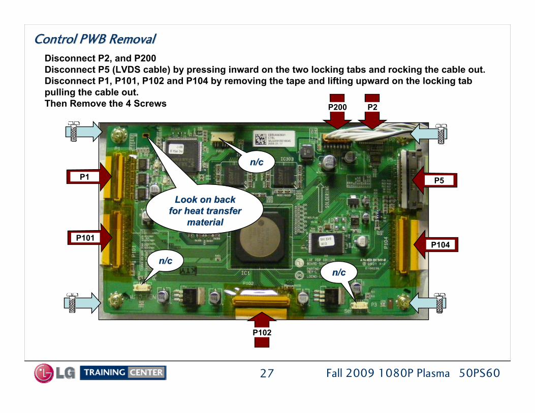
Control PWB RemovalControl PWB Removal
P1
Disconnect P2, and P200Disconnect P5 (LVDS cable) by pressing inward on the two locking tabs and rocking the cable out.Disconnect P1, P101, P102 and P104 by removing the tape and lifting upward on the locking tab pulling the cable out.Then Remove the 4 Screws
P101
P5
P104
P102
P2P200
n/cn/c
n/cn/c
n/cn/c
Look on backLook on backfor heat transfer for heat transfer
materialmaterial

28 Fall 2009 1080P Plasma 50PS60
YY--SUS PWB RemovalSUS PWB Removal
Disconnect P302 and P307.
Disconnect P101 and P309 by removing the tape and lifting upward on the locking tab pulling the cable out.
Then Remove the 10 Screws
Carefully separatethe Y-SUS fromthe Y-DriveUpper and LowerBoards.
P302
P101
P307
P309
n/cn/c

29 Fall 2009 1080P Plasma 50PS60
YY--Drive Upper PWB RemovalDrive Upper PWB Removal
Disconnect P111 and P112.
Disconnect P101, P102, P103 and P104 by lifting up on the locking tab and then lifting up slightly on the FPC to release the small wings on the cable.
Then Remove the 3 Screws
Carefully separatethe Y-Drive fromthe Y-SUS Boards which is connected via P114 and P116.
P112
P102
P111
P116
P114
P101
P104
P103
••Note: All connectors Note: All connectors going to the Ygoing to the Y--SUS board SUS board are fragile.are fragile.
••P114, P116, P214 and P114, P116, P214 and P216. P216.
••Removing and reinserting Removing and reinserting the drive board or the the drive board or the YY--SUS can cause an SUS can cause an intermittent or open intermittent or open connection. connection.
••Investigate these Investigate these connectors carefully after connectors carefully after replacing either the Yreplacing either the Y--SUS SUS or Upper or Lower Yor Upper or Lower Y--Drive Drive boards and resolder if boards and resolder if necessary.necessary.
30 Fall 2009 1080P Plasma 50PS60
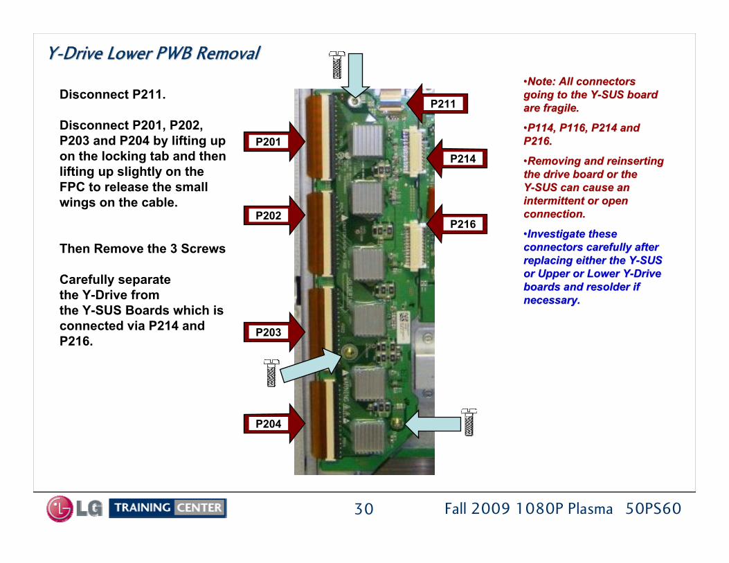
YY--Drive Lower PWB RemovalDrive Lower PWB Removal
Disconnect P211.
Disconnect P201, P202, P203 and P204 by lifting up on the locking tab and then lifting up slightly on the FPC to release the small wings on the cable.
Then Remove the 3 Screws
Carefully separatethe Y-Drive fromthe Y-SUS Boards which is connected via P214 and P216.
P202P216
P214P201
P204
P203
••Note: All connectors Note: All connectors going to the Ygoing to the Y--SUS board SUS board are fragile.are fragile.
••P114, P116, P214 and P114, P116, P214 and P216. P216.
••Removing and reinserting Removing and reinserting the drive board or the the drive board or the YY--SUS can cause an SUS can cause an intermittent or open intermittent or open connection. connection.
••Investigate these Investigate these connectors carefully after connectors carefully after replacing either the Yreplacing either the Y--SUS SUS or Upper or Lower Yor Upper or Lower Y--Drive Drive boards and resolder if boards and resolder if necessary.necessary.
P211

31 Fall 2009 1080P Plasma 50PS60
ZZ--SUS PWB RemovalSUS PWB Removal
Disconnect P100 and P101
Disconnect P102 and P104 by pulling out (to the right) the locking tabs and removing the FPC from the connector.
Then Remove the 8 Screws
Carefully separatethe Z-SUS fromthe Z-SUB P103 and remove.
P104
P102
P103
P101
P100
n/cn/c

32 Fall 2009 1080P Plasma 50PS60
Removing Front Power LED and IR BoardRemoving Front Power LED and IR Board
Power LED PWBFront IR PWB
Screw
To remove the Ft Power LED and Ft IR board,To remove the Ft Power LED and Ft IR board,
Remove the 2 screws in the Front IR PWB Remove the 2 screws in the Front IR PWB
Remove the 1 screw at the bottom of the Power LED PWB.Remove the 1 screw at the bottom of the Power LED PWB.
1
1
2
2
Note, this sNote, this screw has an Oversized washer which locks the board in place.
2
GroundStrap screw
Ground snap
CabinetBottom
Note, the left screw in step 1 has a ground strap Note, the left screw in step 1 has a ground strap lug. Make sure to return it when reinstalling the lug. Make sure to return it when reinstalling the board. This ground snaps into the Bottom Metal.board. This ground snaps into the Bottom Metal.
1
Bottom Metal

33 Fall 2009 1080P Plasma 50PS60
LVDS Cable Connector
Lay the Plasma down carefully on a padded surface.Make sure AC is removed and remove the Back Cover and the Stand.Carefully remove the LVDS Cable P1003 from the Main Board by lifting the Locking Tab upward and pull the ribbon cable free. (See illustration to the right). This prevents possible damage to the cable.
(A) Remove the Stand (4 Screws removed during back removal)Pull the stand out of the stand support bracket.
(B) Remove the Stand Metal Support Bracket (5 Screws). (C) On the Main board, remove connectors P1108, P1101 and P900.
The LVDS connector should already be removed (see above).(D) Remove the 4 screws from the Main Board Mounting Bracket.
(Note: Decorative Plastic Piece on right does not need to be removed)Carefully reposition the Main Board and Mounting Bracket up and off to the right side.
(E) Remove the metal support Braces marked “E”. Note: There is a Left and a Right brace. (3 Screws per/bracket).
(F) Remove the 13 screws holding the Heat Sink.
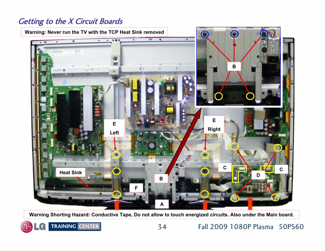
Removing the X Drive Circuit Board Removing the X Drive Circuit Board
PROCEDURE: (See Figure on next page). Flip up the Locking Tab
X-DRIVE PWBs REMOVAL:Disconnect all TCP ribbon cables from the defective X-Drive PWB. Remove the 5 screws holding the PWB in place.Remove the PWB. Reassemble in reverse order. Recheck Va / Vs / VScan / -VY / Z-Bias.
34 Fall 2009 1080P Plasma 50PS60
Getting to the X Circuit BoardsGetting to the X Circuit Boards
A
C
E
Left
F
Heat Sink
Warning: Never run the TV with the TCP Heat Sink removed
Warning Shorting Hazard: Conductive Tape, Do not allow to touch energized circuits. Also under the Main board.
B
C
E
Right
B
D

35 Fall 2009 1080P Plasma 50PS60
50PS60 Plasma Display
This Section will cover Circuit Operation, Troubleshooting and Alignment of the Power Supply, Y-SUS Board, Y Drive Boards, Z-SUS Board, Control Board, Main Board and the X Drive Boards.
At the end of this Section the technician should understand the operation of each circuit board and how to adjust the controls. The technician should be able with confidence to troubleshoot a circuit board failure, replace the defective circuit and perform all necessary adjustments.
CIRCUIT OPERATION, TROUBLESHOOTING AND CIRCUIT ALIGNMENT SECTIONCIRCUIT OPERATION, TROUBLESHOOTING AND CIRCUIT ALIGNMENT SECTION

P102
P101
P103
P104
P202
P201
P203
P204
Control KeysPower Button
50PS60 SIGNAL and VOLTAGE DISTRIBUTION DIAGRAM
Display PanelHorizontal Grids Luminance
P101
FloatingGround
Y-SUS PWB
P312 (FG) P201
P314 (FG)P101
P307P216
M5V, Vs, Va
P811
P814SK101
STB +5V (also AC Voltage Det)
SMPSTurn On
Commands
SMPSPWB
ACInputFilter
P100
SMPS OUTPUT VOLTAGES IN STBY
Set inStand By:STB +5AC Voltage Det
Logic Signals
P1006 P1003
P1101P1005
MAIN PWBSpeakers
X-PWB-RightX-PWB-Left
P201 P202 P203 P204 P205 P206 P301 P302 P303 P304 P305 P306
RGB Logic Signals
VaRGB Logic
Signals
Va
CONTROLPWBP102
LVDS
Y DriveUpper
Z SUS PWB
P101
P200
P104
P232 P211 P311 P331
Display Panel Vertical Address (Color Information)
Display PanelGrids Address
Reset
17V
Relay OnM5 OnVS On
STB5V, +5V, 17V, 12V to Main PWBVs, Va and M5V to Y-SUS, Z-SUSM5V to Control PWB
SMPS OUTPUT VOLTAGES IN RUN
P104
17V
Z Drive Signals
IR, Power LED, Intelligent Sensor
FPCs
FPCs
5V STBY
P103
P214
P111
P211
P112
P116
P114
Drive DataClock (i2c)
P309 Data, Clock (i2c)
P311(V Scan) (5VFG) (FG)
X-PWB-CenterP120 P220 P221 P320P310
P210P121
Va
P5
P2
P110
P812
P813 M5V, Vs, VaNote: Va not used
Note: Va not usedby Y-SUS
P101
P105
P102
P103
P106P1
Note: 17V not usedby Control
17VM5V
FloatingGround
LVDS
3.3V 3.3V 3.3V
FPCs
FPCs
Y DriveLower
Z Drive Signals
5VFG indicates measured from Floating Ground
P313(V Scan) (5VFG) (FG)
5VFG
5VFG
36
+5V, 12VM5V17V, Va, Vs
3.3VKey Board
Pull Up

37 Fall 2009 1080P Plasma 50PS60
(1) Model Name(2) Bar Code(3) Manufacture No.(4) Adjusting Voltage DC, Va, Vs(5) Adjusting Voltage (Set Up / -Vy / Vsc / Ve / Vzb)(6) Trade name of LG Electronics(7) Manufactured date (Year & Month)(8) Warning
Panel Label ExplanationPanel Label Explanation
(9) TUV Approval Mark(10) UL Approval Mark(11) UL Approval No.(12) Model Name(13) Max. Watt (Full White)(14) Max. Volts(15) Max. Amps
(1)(2)(3)(4)(5)(6) (7)
(8)
(9) (10)
(11)(12)
(13)(14)(15)

38 Fall 2009 1080P Plasma 50PS60
ADJUSTMENT ORDER “IMPORTANT”DC VOLTAGE ADJUSTMENTS1) SMPS PWB: Va Vs (Always do SMPS first)2) Y-SUS PWB: Adjust –Vy, Vscan, 3) Z-SUS PWB: Adjust ZBiasWAVEFORM ADJUSTMENTS1) Y-SUS PWB: Set-Up, Set-Down
Adjustment OrderAdjustment Order
It is critical that the DC Voltage adjustments be checked when;1) SMPS, Y-SUS or Z-SUS PWB is replaced.2) Panel is replaced, Check Va/Vs since the SMPS does not come with new panel3) A Picture issue is encountered4) As a general rule of thumb when ever the back is removed
Remember, the Voltage Label MUST be followed, it is specific to the
panel’s needs.
All label references are from a specific panel. They are not the same for every panel
encountered.
The Waveform adjustment is only necessary1) When the Y-SUS PWB is replaced2) When a “Mal-Discharge” problem is encountered3) When an abnormal picture issues is encountered
All Adjustments MUST be done in White Wash

39 Fall 2009 1080P Plasma 50PS60
SWITCH MODE POWER SUPPLY PWB SECTIONSWITCH MODE POWER SUPPLY PWB SECTION
The following section gives detailed information about the SwitcThe following section gives detailed information about the Switch h Mode Power Supply (SMPS) This board develops voltages for all Mode Power Supply (SMPS) This board develops voltages for all other boards.other boards.
The SMPS outputs the following voltages: The SMPS outputs the following voltages:
•• STBY 5V (StandSTBY 5V (Stand--By), By),
•• +5V, 12V when Relay On command arrives +5V, 12V when Relay On command arrives
•• M5V to the Control, YM5V to the Control, Y--SUS and ZSUS and Z--SUS boards when M5 On SUS boards when M5 On command arrivescommand arrives
•• 17V to the Main board when Vs on arrives17V to the Main board when Vs on arrives
•• VS to the YVS to the Y--SUS and ZSUS and Z--SUS boards when Vs on arrivesSUS boards when Vs on arrives
This board has 2 DC adjustments:This board has 2 DC adjustments:
•• (VS) Voltage for Sustain(VS) Voltage for Sustain
•• (Va) Voltage for Address (Va) Voltage for Address

40 Fall 2009 1080P Plasma 50PS60
The Switch Mode Power Supply Board Outputs to the :
VAY-SUS BoardZ-SUS BoardControl Board
Main Board
VS
M5V
(Va = Voltage for Address)Primarily responsible for Panel’s Vertical electrodes (X Boards, TCPs).Va routed to the Y-SUS then to the left X board.
(Vs = Voltage for Sustain)Drives the Panel’s Horizontal Electrodes (Y and Z SUS Boards)
(M5V = Monitor 5 volts) Used to develop Bias Voltages on the Y-SUS, Z-SUS and Control Boards.
17V Audio B+ Supply
+5V Signal Input Circuits
Adjustments
There are 2 adjustments located on the Power Supply Board VA and VS. The 5V VCC is pre-adjusted and fixed. All adjustments are made with relation to Chassis Ground. Use “Full White Raster” 100 IRE. Each panel has its own adjustment values for Va and Vs. Use the Panel’s Voltage Label for reference.
VA
VS
RV901
RV501
Switch Mode Power Supply OverviewSwitch Mode Power Supply Overview
12V Video Processing
5V-STBY Control Circuits

41 Fall 2009 1080P Plasma 50PS60
P811
P812To
Y-SUS ToZ-SUS
F8014A/250V
P813
ToControl
P814
ToMain
SC101
Fuse F101-215A/250V
F3021A/250V
Vs AdjVR901
Va AdjVR501
Hot Ground Symbol
M5VM5VGndVAVAGndGndNCVSVS
IC701
1
SMPS (Switch Mode Power Supply) PWB LayoutSMPS (Switch Mode Power Supply) PWB Layout
1
1
1
VSVS NCGndGndVAVA GndM5VM5V
1~4 M5V5~8 Gnd

42 Fall 2009 1080P Plasma 50PS60
Power Supply Basic OperationPower Supply Basic OperationAC Voltage is supplied to the SMPS Board at Connector SC101 from the AC Input assembly. Standby 5V is developed from 165V source supply (which during run measures 380V measured from the primary fuse F302). This supply is also used to generate all other voltages on the SMPS.
The STBY5V (standby) is B+ for the Sub Micon (IC701) on the SMPS and output at P814 pins 11 and 23 then sent to the Main PWB for Microprocessor (IC1) operation. AC Detect is generated on the SMPS, by rectifying a small sample of the A/C Line at D102 and associated circuitry and routed to the Sub Micon (IC701) where it outputs at pin 15 and sent to P814 pin 18 to the Main Board where it is sensed and monitored by the Main Microprocessor (IC1). The AC Det in this set works differently than most. If AC Det is missing the Microprocessor will turn off the television in about 10 seconds after turn on.This will happen each time turn on is attempted.A new feature included on the side keypad is called a Power Button which opens a ground allowing the “Key On” line of P814 Pin 24 to go high, turning off the 5V STB line defeating the Micro Processor (IC1) on the Main Board and Remote Control Operation. When the Microprocessor (IC1) on the Main Board receives an “ ON “ Command from either the Power button or the Remote IR Signal, it outputs a high called RL ON at Pin 19 of P814. This command causes the Relay Drive Circuit to close both Relays RL102 and RL103 bringing the PFC source up to full power by increasing the 165V standby to 380V run which can be read measuring voltage at Fuse F302 and F801 from “Hot” Ground. At this time the run voltages 12V, and +5V sources become active and are sent to the Main Board via P814 (12V at pins 5 and 6 and 5V at pins 9,10, and 12). The 5V detect line from the Main Board to the SMPS Board can be measured at pin 17 of P814. It is not used.The next step is for the Microprocessor (IC1) on the Main Board to output a high on M5V ON Line to the SMPS at P814 Pin 21 which is sensed by the Sub Micon (IC701) turning on the M5V line and output at P811 and P812 pins 9 and 10 to the Y and Z SUS boards and P813 pins 1~4 to the Control board. Full Power occurs when the Microprocessor (IC1) on the Main Board brings the VS-ON line high at Pin 20 of P814 of the SMPS Board. VS-ON is routed to the Sub Micon (IC701) which turns on the 17V Audio, VA, and the VS supplies. VA and VS output at P811 to the Y-SUS board and P812 to the Z-SUS board. (VA pins 6 and 7 and VS pins 1 and 2 of either connector) the 17V Audio supply outputs to the Main board at P814 pins 1 and 2.AUTO GND Pin 22 of P814: This pin is grounded on the Main board. When it is grounded, the Sub Micon IC701 works in the normal mode. Meaning it turns on the power supply via commands sent from the Main board. When this pin is floated (opened), it pulls up and turns the Sub Micon IC701 on in the Auto mode. In this state, the Sub Micon turns on the power supply in stages automatically. A load is necessary to regulate the 17V with the SMPS disconnected. This is a good test if the Main board is suspect.

50PS60 POWER SUPPLY START UP SEQUENCE50PS60 POWER SUPPLY START UP SEQUENCE
43
AC In
Stand By 5V
Power OnRemote Or Key
AC Det.
Reset
MAIN PWB
Relay On
12V Video
MicroprocessorIC1
M5V Reg
Vs Reg
Va Reg
5V/12V Regulators
5V Det.
5V Reg
StandBy 5V Reg
1
23
67 9 13
At point TV is in Stand-By state. It isEnergy Star Compliant.Less than 1 Watt
6
6
9
In Stand-By Primary side is 163VIn Run (Relay On) Primary side is 386V
4
4
14
Control PWB
X PWBLeft
14
3.3V Reg
2
5V Det.
Relay On
Y-SUS PWB Z-SUS PWB
10
17V 17V17V17V5VFGVa
Y DRIVEUpper
X PWBCenter
X PWBRight
Y DRIVELower
STBY 5V
M5V M5V M5VVsVaVsVa
15
11 111112
16 16
15
3.3V
12
13
9
15
15 15
5
25
Other
Circuits
Vs
Va
13
14
16 1015 16 10 10
15
15
Standby 5V will not be output if the
Power Button is off.
Power Button
OnOff
Front IRBoard
POWER SUPPLY(SMPS)
NotUsed
AC Det.If missing, set turns off within 10 sec.
12V5V
17V Audio
17V
17V Reg
8
+5V HDMI EDIDAnd other input circuits
M5VOn Vs
On
5VFloating
Gnd
14

44 Fall 2009 1080P Plasma 50PS60
SMPS AdjustmentsSMPS Adjustments
These two voltages are adjustable and should be adjusted to thecorrect values as indicated by your specific panel label. Example shown on the right.
Set should be in “Full White Raster” and Heat Run 10 Minutes.
1) VS ADJUST:Connect DVM to pin 1 or 2 of P812. Adjust VR901 until the voltage matches your panel’s voltage label.
2) VA ADJUST:Connect DVM to pin 6 or 7 of P812. Adjust VR501 until the voltage matches your panel’s voltage label.
VS and VA adjustment resistors are shown in the drawing below.VR901 is the VS adjustment pot.VR501 is the VA adjustment pot.

50PS60 SMPS STATIC TEST UNDER LOAD
1 2
5
or
8or4 or
Using two 100 Watt light bulbs, attach one end to Vs and the other end to ground. Apply AC to SC101. If the light bulbs turn on and VS is the correct voltage, allow the SMPS to run for several minutes to be sure it will operate under load. If this test is successful and all other voltages are generated, you can be fairly assured the power supply is OK. Note: To be 100% sure, you would need to read the current handling capabilities of each power supply listed on the silk screen on the SMPS and place each supply voltage under the appropriate load.
Vs
GndCheck Pins 6 or 7
for Va voltage
Note: This SMPS will run without a load, however if the Vs is not loaded, the 17V will pulsate up and down. It is always best to test the SMPS under a load using the 2 light bulbs.
P811
P8141
2
P813
U701
P812
T301
SC101
10) M5V 9) M5V 8) Gnd 7) VA 6) VA 5) Gnd 4) Gnd 3) NC 2) VS 1) VS
23
24
Check Pins 11 or 23 for 5V SBY
Check Pin 18 for AC Det (5V)
If AC Det is missing, the TV will come on then shut off within 10 Sec.This will happen each time the TV is turned on.
Provided the Power Button is closed, any time AC is applied to the SMPS, STBY 5V and AC DET should be present.
10) M5V 9) M5V 8) Gnd 7) VA 6) VA 5) Gnd 4) Gnd 3) NC 2) VS 1) VS 1,2,3,4) M5V
5,6,7,8) Gnd
100W
100W
Pins
Check Pin 9,10,12 for (+5V)
Check Pins 1~4 forM5V
Check Pins 1 or 2 for17V
Check Pins 5 or 6 for12V
P814
P813
P812
Check Pins 1 or 2for Vs voltage
P811
45

50PS60 Power Supply TroubleshootingUsing two 100 Watt light bulbs, attach one end to Vs and the other end to ground. Apply AC to SC101. If the light bulbs turn on and VS is the correct voltage, allow the SMPS to run for several minutes to be sure it will operate under load. If this test is successful and all other voltages are generated, you can be fairly assured the power supply is OK. Note: To be 100% sure, you would need to read the current handling capabilities of each power supply listed on the silk screen on the SMPS and place each supply voltage under the appropriate load.
This Power Supply can be powered on sequentially for understanding of the operation and for troubleshooting purposes. When the supply is operational in its normal state the Auto Ground line at Pin 22 of P814 is held to ground by the Main Board.When the Power Button is in the off state the Standby 5V Supply will be at 0v, the Key On Line at Pin 24 will be 4.3V. When the Power Button is pressed on, the Key On Line is grounded which allows the 5V Standby to go to 5V.
46
(A) Grounding both the Auto Gnd and the Key On Lines will allow the supply to be powered up one section at a time. (B) Add a 100Ω ¼ watt resistor from 5V Standby to RL_ON and the 12V and 5V Run Lines will become active. (C) Add a 100Ω ¼ watt resistor from 5V Standby to M5V_ON to make the Main 5V Line operational. (D) Add a 100Ω ¼ watt resistor from 5V Standby to Vs_On to make the 17V, Va and Vs lines operational. (See note at top)
Note: Placing the two 100 Watt light bulbs from Vs to Ground will assure the power supply will regulate with a load and that the 17V will be stable. Without out this load, the 17V will pulsate up and down.
1 2
5
or
8or4 or
Vs
GndP811
P8141
2
P813
U701
P812
T301
SC101
10) M5V 9) M5V 8) Gnd 7) VA 6) VA 5) Gnd 4) Gnd 3) NC 2) VS 1) VS
23
24
10) M5V 9) M5V 8) Gnd 7) VA 6) VA 5) Gnd 4) Gnd 3) NC 2) VS 1) VS
1,2,3,4) M5V5,6,7,8) Gnd
100W
100W
Pins
P814 31 75 119 1513 1917 21
42 86 1210 1614 2018 22
17V Gnd 12V Gnd +5V
17V Gnd 12V Gnd +5V +5VACDet
KeyOn
STBY 5VGnd
Gnd
Gnd5VDet
AutoGnd
100Ω
23
24
V SO n
B
C
D100Ω
A
100Ω
M5 O
n
Relay O
n
STBY 5V

47 Fall 2009 1080P Plasma 50PS60
Diode Mode Readings taken with all connectors Disconnected. Black lead on Gnd. DVM in Diode Mode.
P814 Pins ID, Voltages and Diode Mode Measurements for the SMPSP814 Pins ID, Voltages and Diode Mode Measurements for the SMPS
Open3.3V0VM5 ON21
Open5V5VStby 5V23
Open3.3V0VRL On19
1.45V4.8V0V5V Det17*
GndGndGndGnd15
GndGndGndGnd13
Open5.15V5.15VStby 5V11
1.2V5.15V0V+5V9
GndGndGndGnd7
Open12V0V12V5
GndGndGndGnd3
2.2V17.3V0V17V1*
Diode ModeRun STBYLabelPin
OpenGndGndAuto Gnd22
Open*0V*0VKey On24*
Open3.2V0VVS On20
1.45V5V5VAC Det18*
n/cn/cn/cn/c16
GndGndGndGnd14
1.2V5.15V0V+5V12
1.2V5.15V0V+5V10
GndGndGndGnd8
Open12V0V12V6
GndGndGndGnd4
2.2V17.3V0V17V2*
Diode ModeRun STBYLabelPin
P814 CONNECTOR “SMPS" to “Main PWB" P1006
* Pin 24: When the Power Button is opened, • Pin 24 pulls up to 4.3V.• Stand-By 5V turns off. AC-Det remains.
* Pin 1 and 2: 17V If Vs is unloaded will pulsate.Turned on by Vs On Command.
* Pin 18: AC DET if missing will cause the set to turn off after 10 seconds.
* Pin 17: 5V Det not used.
* Pins 9, 10, 12: (+5V) Turned on by Relay On Command.

48 Fall 2009 1080P Plasma 50PS60
SK101 and P811 Pin ID and VoltagesSK101 and P811 Pin ID and VoltagesVoltage and Diode Mode Measurements for the SMPS.
0.86V
0.86V
n/c
Open
Open
Gnd
Gnd
n/c
Open
Open
Diode ModeDisconnected
* Note: This voltage will vary in accordance with Panel Label
0.74V5V0VM5V10
0.74V5V0VM5V9
n/cn/cn/cn/c8
Open*65V0VVa7
Open*65V0VVa6
GndGndGndGnd5
GndGndGndGnd4
n/cn/cn/cn/c3
Open*195V0VVs2
Open*195V0VVs1
Diode ModeConnectedRun STBYLabelPin
SC101 AC INPUT
Standby Run Diode ModeConnector Pin Number
SC101 120VAC 120VAC Open1 and 3
Diode Mode Readings taken with all connectors Disconnected. Black lead on Gnd. DVM in Diode Mode.
P811 CONNECTOR "Power Supply PWB“ to Y-SUS P302

49 Fall 2009 1080P Plasma 50PS60
P812 Pin ID and VoltagesP812 Pin ID and VoltagesVoltage and Diode Mode Measurements for the SMPS.
0.86V
0.86V
Gnd
Open
Open
Gnd
Gnd
n/c
Open
Open
Diode ModeDisconnected
* Note: This voltage will vary in accordance with Panel Label
0.74V5V0VM5V10
0.74V5V0VM5V9
Gndn/cn/cn/c8
Open*65V0VVa7
Open*65V0VVa6
GndGndGndGnd5
GndGndGndGnd4
n/cn/cn/cn/c3
Open*195V0VVs2
Open*195V0VVs1
Diode ModeConnectedRun STBYLabelPin
Diode Mode Readings taken with all connectors Disconnected, Unless specified. Black lead on Gnd. DVM in Diode Mode.
P812 CONNECTOR "Power Supply PWB“ to Z-SUS P101

50 Fall 2009 1080P Plasma 50PS60
P813 Connector Pin ID and VoltagesP813 Connector Pin ID and VoltagesVoltage and Diode Mode Measurements for the SMPS.
GndGndGndGnd8
GndGndGndGnd7
GndGndGndGnd6
GndGndGndGnd5
0.75V5V0VM5V4
0.75V5V0VM5V3
0.75V5V0VM5V2
0.75V5V0VM5V1
Diode ModeConnectedRun STBYLabelPin
Diode Mode Readings taken with all connectors Disconnected. Black lead on Gnd. DVM in Diode Mode.
P813 CONNECTOR "Power Supply PWB“ to “Control PWB” P2001
NOTE: The Black wire on P813 Connector is not pin 1.
P813

51 Fall 2009 1080P Plasma 50PS60
YY--SUS PWB SECTIONSUS PWB SECTION
The following section gives detailed information about the YThe following section gives detailed information about the Y--SUS SUS board. This board develops the board. This board develops the ““Panel Sustain SignalsPanel Sustain Signals”” and delivers and delivers the Luminance signals to the panel. The Ythe Luminance signals to the panel. The Y--SUS board receives the SUS board receives the waveform development signals from the Control board. The Ywaveform development signals from the Control board. The Y--SUS SUS also develops additional voltages via internal switch mode poweralso develops additional voltages via internal switch mode powersupplies. 15V, floating ground 5V, VSC voltages and supplies. 15V, floating ground 5V, VSC voltages and ––Vy voltages.Vy voltages.
This board has 4 adjustments, 2 DC and 2 Waveform:This board has 4 adjustments, 2 DC and 2 Waveform:
Board Receives its main B+ from the:Board Receives its main B+ from the:
• 2 DC: VSC (VSCAN) AND –Vy (DD-VAR)
• 2 Waveform: Set-Up1 and Set-Dn1
• Switch Mode Power Supply sends VS
• Switch Mode Power Supply sends M5V
52 Fall 2009 1080P Plasma 50PS60
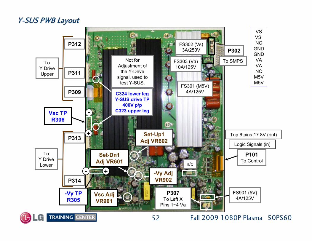
YY--SUS PWB LayoutSUS PWB Layout
P312
FS901 (5V)4A/125V
Vsc AdjVR901
VSVS NC
GNDGNDVAVANC
M5VM5V
P311
P313
P314
P302
To SMPS
P101To Control
P309
-Vy TPR305
+
-
+-
FS302 (Vs)3A/250V
FS303 (Va)10A/125V
n/c
Logic Signals (in)
Top 6 pins 17.8V (out)
Set-Dn1Adj VR601
-Vy AdjVR902
Set-Up1Adj VR602
P307To Left X
Pins 1~4 Va
ToY DriveUpper
ToY DriveLower
Vsc TPR306
C324 lower legY-SUS drive TP
400V p/pC323 upper leg
Not for Adjustment of the Y-Drive
signal, used to test Y-SUS.
FS301 (M5V)4A/125V

50PS60 (50H3 Panel) Y-SUS PWB LAYOUT50PS60 (50H3 Panel) Y-SUS PWB LAYOUT
53
R305-VY TP VR901
VSCAN
P309
VR601SET-dn1
VR602SET-up1
R306VSC TP
P312
P311
P313
P314 P101
P302
FS302Vs
FS303Va
FS901M5V
P307
VR902DD_Var (-Vy)
(-) (+)
(-)
(+)
FS301M5V

54 Fall 2009 1080P Plasma 50PS60
YY--SUS SUS ––Vy and VSC AdjustmentsVy and VSC Adjustments
PROCEDURE: (See figures for locations)
4) Adjust –Vy using VR902. Measured across –Vy TPs R305. Match your specific Panel’s Voltage label ±1V.
1) Pre-Heat unit for at least 10 Minutes before making adjustments. Vs and Va adjustments complete.
2) Place unit into White Wash from the Customer’s Menu for all adjustments.3) Be sure to use all adjustment values as indicated on your panel’s
voltage label in the upper right of the panel. (Example shown above)
5) Adjust VSC using VR901.Measured across VSC TPs R306. Match your specific Panel’s Voltage label ±1V.
Location Bottom Center
-Vy VR902
VSC VR901
VSC TP R306
-Vy TP R305
Location Lower left
Location Lower Center

55 Fall 2009 1080P Plasma 50PS60
To set the Oscilloscope up for External Trigger first connect a Scope Probe set on direct to the External Input Jack.Next set the External Jack for AC Coupling either positive or negative slope, use the Trigger Menu on the Scope. Finally you will need to set the Trigger Level press the Trigger View and set the level as indicated in the picture below.
External Triggering of the Oscilloscope allows for a Stable Display of both the Y and Z SUS Output Waveforms regardless of how distorted the waveforms may be, allowing the wave shape and phasing to be easily examined.
Observing the Y and Z Observing the Y and Z SUSSUS Output WaveformsOutput Waveforms
External Trigger Source
55
T
Trigger Level Adjust
VS_DA Test Point:
• Located on the Control Board just to the right of the MCM Chip and above the EEPROM IC6.
This TP may be used as an external trigger source for locking the waveform on the Oscilloscope

56 Fall 2009 1080P Plasma 50PS60
YY--Drive Signal Test PointsDrive Signal Test Points
Overall signal observed 2mS/div
Highlighted signal from waveform above observed
100uSec/div
Highlighted signal from waveforms above observed
50uS/div
Either test point is OK to use.NOTE: The Waveform Test Points are fragile. If by accident the land is torn and the run lifted, make sure there are no lines left to right in the screen picture.
50uS 510V p/p
Y-Drive PWB Test Points (Middle of bottom
Y-Drive Board)
78V RMS

57 Fall 2009 1080P Plasma 50PS60
Observing (Capturing) the YObserving (Capturing) the Y--Drive Signal for SetDrive Signal for Set--up or Setup or Set--downdown
Fig 1:As an example of how to lock in to the Y-Drive Waveform. Fig 1 shows the signal locked in at 2ms per/div.Note the blanking sections.The signal for Set-Up / Down adjustment is outlined within the Waveform
Fig 2:At 100us per/div. the signal for Set-Up / Down adjustment is now easier to recognize. It is outlined within the Waveform
Fig 3:At 50uSec per/division, the adjustment for SET-UP or SET-DOWN can be made.
Note: When actually performing the adjustments,The portion of the waveform being adjusted can beZoomed in on by increasing the speed of the scope.
FIG12mS
FIG2100uS
Outlined AreaBlanking
FIG350uS
Set must be in “WHITE WASH” All other DC Voltage adjustments should have already been made.
Set Up
Set Down
Area tobe adjusted
Area tobe adjusted

58 Fall 2009 1080P Plasma 50PS60
YY--SUS (Y Drive Waveform SetSUS (Y Drive Waveform Set--Up and SetUp and Set--Down Adjustments)Down Adjustments)
PROCEDURE: (See figure to the right for locations)
Oscilloscope TP on the “Waveform” TPs on the Y-Drive PWB.
3) SET-UP ADJUSTMENT VR602:Adjust VR602 while observing area (A) and set the flat portion to10uSec ± 5uSec. While observing only the peak of the waveform,turn the pot CW which will cause the peak to dome to the left of the flat portion. CCW will cause the peak to decrease in amplitude. Turn CW until the dome appears, then back off CCW.
4) SET-DOWN ADJUSTMENT VR601:Adjust VR601 while observing area (B) and set to 160uSec ± 5uSec.
1) Pre-Heat unit for at least 10 Minutes before making adjustments.Vs, Va, -Vy and VSC adjustments should be completed.
2) Place unit into White Wash from the Customer’s Menu for all adjustments.
Lower Center Of PWB
V Set-Up AdjVR602
V Set-Dn AdjVR601

59 Fall 2009 1080P Plasma 50PS60
V Set Up Too High or LowV Set Up Too High or LowAll Waveforms taken at 50V per/div, 50uSec per/div
Ramp (Vset UP) too high
Ramp (Vset UP) too low
Vset DN too high
Vset DN too low
NOTE: If Vset DN too high, this set will go to excessive bright, then shutdown. To correct, remove the LVDS from control PWB and make necessary adjustments.

60 Fall 2009 1080P Plasma 50PS60
Y SUS Block DiagramY SUS Block Diagram
Circuits generate Y Sustain Waveform
Distributes M5V and 15V to Control Board15V Generated by on board SMPS
Distribute VA to X Boards Receive M5V, Va, Vsfrom SMPS
FETs amplify Sustain Waveform
Generates Floating Ground5V by on board SMPS
To Y Drive Boards
Generates Vsc and -Vyfrom Vs or M5V by internal SMPS Also controls Set Up/Down via adj.
Logic signals needed to generate drive waveform
M5V, Vs, Va from SPS
Y Scan Signal to Y Drive Board

61 Fall 2009 1080P Plasma 50PS60
Diode Mode Readings taken with all connectors Disconnected unless specified. Black lead on Gnd. DVM in Diode Mode.
YY––SUS P302 to SMPS P811 Plug InformationSUS P302 to SMPS P811 Plug Information
1.14V
1.14V
Gnd
Open
Open
Gnd
Gnd
n/c
Open
Open
Diode ModeDisconnected
0.74V5VM5V10
0.74V5VM5V9
Gndn/cn/c8
Open*65VVa7
Open*65VVa6
GndGndGnd5
GndGndGnd4
n/cn/cn/c3
Open*195VVs2
Open*195VVs1
Diode ModeConnectedRun LabelPin
P302 CONNECTOR "Y-SUS" to "Power Supply PWB" P811
* Note: This voltage will vary in accordance with Panel Label
Voltage and Diode Mode Measurements.Note: There are no Stand-By Voltages to this board.
P302
1

62 Fall 2009 1080P Plasma 50PS60
Diode Mode Readings taken with all connectors Disconnected. Black lead on Gnd. DVM in Diode Mode.
YY--SUS P307 to Left X Drive P121 Plug InformationSUS P307 to Left X Drive P121 Plug Information
GndGndGnd7GndGndGnd6NCNCNC5
Open*65VVA4Open*65VVA3Open*65VVA2Open*65VVA1
Diode ModeRun LabelPin
* Note: This voltage will vary in accordance with Panel Label
P307 CONNECTOR "Y-SUS PWB" to "X-Drive” Left P121
Voltage and Diode Mode Measurements.Note: There are no Stand-By Voltages to this board.
1
P307

Top 6 pins are 17V to Control then to Z-SUS Control does not use 17V
DELTA_VY_ON_OFFGND
26
DELTA_VY127
GND28
SET_UP229
GND30
SET_UP131
GND32
SET_DN2333435 GND
41 DELTA_VY242 GND43 ER_UP44 GND45 ER_DN46 GND47 SUS_UP484950 GND
SUS_DNGND
36 SET_DN137 CTRL_OE38 GND39 PASS_TOP40 GND
12345678910111213141516171819202122232425DELTA_VY_ON_OFF
GNDDELTA_VY1
GNDSET_UP2
GNDSET_UP1
GNDSET_DN2
GND
DELTA_VY2GND
ER_UPGND
ER_DNGND
SUS_UP
GNDSUS_DN
GND
SET_DN1CTRL_OE
GNDPASS_TOP
GND
P101Y-SUS PWB
P1Control PWB
0.7VGnd
0.68VGnd0V
Gnd0.1VGnd4.9VGnd
3.48V0V
Gnd1.4VGnd0.7VGnd0.2VGnd0.1VGnd
0.1~0.4VGnd4V
Gnd
1 15V2 15V3 15V4 15V5 15V6 15V7 NC8 OC2_ODD9 GND10
CLK11
GND12
DATA_ODD13
GND14
DATA_EVEN151617
STB18
GND1920
GNDGND
OC2_EVEN2122 GND
GND23OC1_EVEN24GND25
OC1_ODDGND
26272829303132333435
41424344454647484950
3637383940
15V15V15V15V15V15VNC
OC2_ODDGND
CLKGND
DATA_ODDGND
DATA_EVEN
STBGND
GNDGND
OC2_EVENGNDGND
OC1_EVENGND
OC1_ODDGND
P101Y-SUS PWB
P1Control PWB
17.8V17.8V17.8V17.8V17.8V17.8V
NC2.84VGnd
1.87VGnd0.3VGnd0V
Gnd0V
GndGnd4.3VGnd2.8VGndGnd
1.85VGnd
Top 25 Pins Bottom 25 Pins
Pin 50 on Y-SUS is Pin 1 on Control Y-SUS P101 to Control P1 Connector Layout
Y-SUS P101 to Control P1 Connector Layout
63

64 Fall 2009 1080P Plasma 50PS60
1.44V1.85VOC1_EVEN24
GndGndGND23
GndGndGND22
1.44V2.8VOC2_EVEN21
GndGndGND20
GndGndGND25
1.44V4.3VSTB19
GndGndGND18
GndGndGND17
1.44V0VDATA_EVEN16
GndGndGND15
1.44V0VDATA_ODD14
GndGndGND13
1.44V0.3VCLK12
GndGndGND11
1.44V1.87VOC1_ODD10
GndGndGND9
1.44V2.84VOC2_ODD8
NCNCNC7
Open17.8V15V6
Open17.8V15V5
Open17.8V15V4
Open17.8V15V3
Open17.8V15V2
Open17.8V15V1
Diode ModeRun LabelPin
1.44V0.1VER_DN45
GndGndGND46
1.44V0.1~0.4VSUS_UP47
GndGndGND48
1.44V4VSUS_DN49
GndGndGND50
GndGndGND44
1.44V0.2VER_UP43
GndGndGND42
1.44V0.7VDELTA_VY241
GndGndGND40
1.44V1.4VPASS_TOP39
GndGndGND38
1.44V0VCTRL_OE37
1.44V3.48VSET_DN136
GndGndGND35
1.44V4.9VSET_DN234
GndGndGND33
1.44V0.1VSET_UP132
GndGndGND31
1.44V0VSET_UP230
GndGndGND29
1.44V0.68VDELTA_VY128
GndGndGND27
1.44V0.7VDELTA_VY_ON_OFF26
Diode ModeRun LabelPin
YY--SUS P101 to Control P1 Connector InformationSUS P101 to Control P1 Connector Information Pin 1 on Control is Pin 50 on Y-SUS
Voltage and Diode Mode Measurement (No Stand-By Voltages)
65 Fall 2009 1080P Plasma 50PS60
Y Y SUSSUS Floating Ground 5V (5VFG) and Scan Input CheckFloating Ground 5V (5VFG) and Scan Input Check
Black Lead: 0.76VBlack Lead: 0.76V Red Lead: OpenRed Lead: Open
Checked from Floating Gnd.Checked from Floating Gnd.YY--Drive boards connected.Drive boards connected.
YY--SUS SUS P311P311
YY--SUS SUS P313P313
Floating Floating GroundGround
5V FG5V FG
VSCANVSCANn/cn/c
Floating Floating GroundGround
5V FG5V FG
VSCANVSCANn/cn/c
5V FG:5V FG:
VSCAN:VSCAN:
Diode Check means the Digital Volt Meter is in Diode Mode.
1
1
Red Lead: 0.6VRed Lead: 0.6VBlack Lead: 0.5VBlack Lead: 0.5V
••Note: All connectors going to the YNote: All connectors going to the Y--SUS board are fragile.SUS board are fragile.
••P114, P116, P214 and P216. P114, P116, P214 and P216.
••Removing and reinserting the drive board or the YRemoving and reinserting the drive board or the Y--SUS can SUS can cause an intermittent or bad connection. cause an intermittent or bad connection.
••Investigate these connectors carefully after replacing either Investigate these connectors carefully after replacing either the Ythe Y--SUS or Upper or Lower YSUS or Upper or Lower Y--Drive boards and resolder if Drive boards and resolder if necessary.necessary.

66 Fall 2009 1080P Plasma 50PS60
Diode Mode Readings taken with all connectors Disconnected. Black lead on Floating Gnd. DVM in Diode Mode.
YY--SUS Connectors P311 SUS Connectors P311 –– P314 to YP314 to Y--Drive InformationDrive Information
FGndFGnd*FGnd6~12
1.3V5V5VFG4~5
n/cn/cn/c3
2.7V140VVScan1~2
Diode ModeRun LabelPin
Note: All Voltage Measurement taken from Floating Ground
2.7V140VVScan11~12
n/cn/cn/c10
1.3V5V5VFG8-9
FGndFGnd*FGnd1~7
Diode ModeRun LabelPin
Voltage and Diode Check Measurements.This board has no Stand-By voltage.
All Pins are Floating Ground
P312 CONNECTOR “Y-SUS to “Upper Y-Drive " P114
All Pins are Floating Ground
P314 CONNECTOR “Y-SUS”to “Lower Y-Drive " P216
P313 CONNECTOR “Y-SUS " to “Lower Y-Drive " P214
* Note: (FGnd) Floating Ground
P311 CONNECTOR “Y-SUS " to “Upper Y-Drive " P116
* Note: (FGnd) Floating Ground

67 Fall 2009 1080P Plasma 50PS60
Y DRIVE UPPER AND LOWER PWB SECTIONY DRIVE UPPER AND LOWER PWB SECTION
The following section gives detailed information about the Y Drive boards (Upper and Lower). These boards deliver the “Y Drive Sustain Signals” to the Panel’s horizontal electrodes, (This determines the Vertical resolution of the panel). Each Y Drive board contains 6 buffers (12 total) driving 8 flexible ribbon cables connecting 1080 horizontal electrodes.These boards have no DC adjustments.
These boards receives their main B+ from the YThese boards receives their main B+ from the Y--SUS PWB:SUS PWB:
•• Floating ground 5V from the Switched Mode Power Floating ground 5V from the Switched Mode Power Supply on the YSupply on the Y--SUS board.SUS board.(Must be measured from the Floating Ground). (Must be measured from the Floating Ground).
•• Y Scan signal (over 500V peak/peak from the YY Scan signal (over 500V peak/peak from the Y--SUS board).SUS board).
•• Logic signals from the Control board, routed through YLogic signals from the Control board, routed through Y--SUS.SUS.

68 Fall 2009 1080P Plasma 50PS60
Y Drive Upper and Lower PWB LayoutY Drive Upper and Lower PWB Layout
Y Drive UpperY Drive Upper
P112P112
P111P111
P114P114
P116P116
P101P101
P102P102
P103P103
P104P104
FPCFPC
FPCFPC
FPCFPC
FPCFPC
Y Drive LowerY Drive Lower
P214P214
P216P216
P211P211
P201P201
P202P202
P203P203
P204P204
FPCFPC
FPCFPC
FPCFPC
FPCFPC
Note: All connectors Note: All connectors going to the Ygoing to the Y--SUS SUS board are fragile.board are fragile.
P114, P116, P114, P116, P214 and P216. P214 and P216.
Removing and Removing and reinserting the drive reinserting the drive
board or the Yboard or the Y--SUS can SUS can cause an intermittent or cause an intermittent or
open connection. open connection.
Investigate these Investigate these connectors carefully connectors carefully after replacing either after replacing either the Ythe Y--SUS or Upper SUS or Upper
or Lower Yor Lower Y--Drive Drive boards and resolder boards and resolder
if necessary.if necessary.
69 Fall 2009 1080P Plasma 50PS60
Y Drive Upper and Lower PWB Connector InformationY Drive Upper and Lower PWB Connector Information
Y Drive UpperY Drive Upper Y Drive LowerY Drive Lower
P112P112
P111P111
P114P114
P116P116
P214P214
P216P216
P211P211
All control signals All control signals input from Yinput from Y--SUSSUS
All control signals for All control signals for lower drive boardlower drive board
Y Drive (V Scan) signal in Y Drive (V Scan) signal in on bottom two pins 1 and 2.on bottom two pins 1 and 2.
Y Drive (V Scan) signalY Drive (V Scan) signalin on top two pins 11 and 12.in on top two pins 11 and 12.
All Pins Floating GroundAll Pins Floating Ground
All Pins Floating GroundAll Pins Floating Ground
Floating Ground 5V pins 8 and 9Floating Ground 5V pins 8 and 9
Floating Ground 5V Floating Ground 5V pins 4 and 5.pins 4 and 5.
All control signals for All control signals for lower Y Drive boardlower Y Drive board
70 Fall 2009 1080P Plasma 50PS60
Y Drive Upper and Lower PWB Chocolate Piece LocationsY Drive Upper and Lower PWB Chocolate Piece Locations
Y Drives RemovedY Drives Removed
ChocolateChocolate
Chocolate pieces are behind Chocolate pieces are behind both Yboth Y--Drive boards.Drive boards.
Pay attention and make sure Pay attention and make sure to replace these pieces if the to replace these pieces if the board is removed.board is removed.
Note: When removing either Note: When removing either YY--Drive board, these Drive board, these Chocolate pieces will Chocolate pieces will ““StickStick””making the board feel as making the board feel as thought its still attached.thought its still attached.
Note the PWB standNote the PWB stand--off. The off. The top of the standtop of the stand--off has a off has a collar which enters the PWB collar which enters the PWB screw hole. The board must screw hole. The board must be lifted up slightly to clear be lifted up slightly to clear these collars before it can be these collars before it can be removed.removed.
ChocolateChocolate
StandStand--OffOff

71 Fall 2009 1080P Plasma 50PS60
Y Drive Removing the Flexible Printed CircuitsY Drive Removing the Flexible Printed Circuits
Flip the locking tab up Flip the locking tab up to unlock the FPC from to unlock the FPC from the connectorthe connector
Slide a thin plastic Slide a thin plastic object under either end object under either end of the FPC and lift up of the FPC and lift up gently releasing the tab.gently releasing the tab.
TabTab
TabTab
Gently pull the FPC Gently pull the FPC from the connector.from the connector.
When reinserting the When reinserting the FPC, make certain that FPC, make certain that both tabs are seated both tabs are seated correctly before correctly before attempting to lockattempting to lock
Gap (Tab exposed)Gap (Tab exposed)
No Gap (Tab seated)No Gap (Tab seated)

72 Fall 2009 1080P Plasma 50PS60
Y Drive Floating Ground 5V and Scan Input CheckY Drive Floating Ground 5V and Scan Input Check
BL: 0.76VBL: 0.76V RLRL: Open: OpenDiode Mode Check: All checks from Floating Gnd.
BL = Black Lead on test point red lead on FG.RL= Red Lead on test point black lead on FG.
Checked from Floating GndChecked from Floating Gnd
Y Drive Upper P116Y Drive Upper P116 Y Drive Upper P214Y Drive Upper P214
Floating Floating GroundGround
5V FG5V FG
VSCANVSCANn/cn/c
Floating Floating GroundGround
5V FG5V FG
VSCANVSCANn/cn/c
BL: 0.60VBL: 0.60V RLRL: Open: Open5V FG5V FG
VSCANVSCAN
Diode Check means the Digital Volt Meter is in Diode Mode, all connectors to PWB are removed.
11
These are These are fragile fragile
connectionsconnections
These are These are fragile fragile
connectionsconnections

73 Fall 2009 1080P Plasma 50PS60
Diode Mode Readings taken with all connectors Disconnected. Black lead on Floating Gnd. DVM in Diode Mode.
Y Drive Connectors P116 Y Drive Connectors P116 –– P214 to YP214 to Y--SUS InformationSUS Information
FGndFGnd*FGnd6~12
Open5V5VFG4~5
n/cn/cn/c3
Open140VVScan1~2
Diode ModeRun LabelPin
Note: All Voltage Measurement taken from Floating Ground
Open140VVScan11~12
n/cn/cn/c10
Open5V5VFG8-9
FGndFGnd*FGnd1~7
Diode ModeRun LabelPin
Voltage and Diode Check Measurements.This board has no Stand-By voltage.
All Pins are Floating Ground
P114 CONNECTOR Upper"Y-Drive" to “Y-SUS" P312
All Pins are Floating Ground
P216 CONNECTOR Lower"Y-Drive" to “Y-SUS" P314
P214 CONNECTOR “Lower Y-Drive" to “Y-SUS" P313
* Note: (FGnd) Floating Ground
P116 CONNECTOR “Upper Y-Drive" to “Y-SUS" P311
* Note: (FGnd) Floating Ground

74 Fall 2009 1080P Plasma 50PS60
Y Drive Upper P111 CheckedY Drive Upper P111 Checked
8
7
Floating GroundFloating Ground
12
Bottom of PWBBottom of PWB
Same as 6
below
4 6
3 5
OC1-T-B-Even
OC2-T-Odd
CLK-T
STB-T
OC2-T-Even
OC1-T-B-OddOC1-T-B-Even
OC2-T-Odd
CLK-T
STB-T
OC2-T-Even
Data-Even
Data-Odd
OSC1-T-B-Odd
Scan (Y Drive Signal)Scan (Y Drive Signal)
5V Floating Ground5V Floating GroundBL: 0.6VBL: 0.6V RLRL: Open: Open
Diode Mode Check: All checks from Floating Gnd.
BL = Black Lead on test point red lead on FG.RL= Red Lead on test point black lead on FG.
BL: 0.76VBL: 0.76V RLRL: Open: Open
BL: 0.87VBL: 0.87V
BL: 0.87VBL: 0.87V
BL: 0.85VBL: 0.85V
BL: 0.85VBL: 0.85V
BL: 0.87VBL: 0.87V
BL: 0.84VBL: 0.84V
BL: 0.84VBL: 0.84V
BL: 0.87VBL: 0.87V
BL: 0.87VBL: 0.87V
BL: 0.87VBL: 0.87V
BL: 0.85VBL: 0.85V
BL: 0.85VBL: 0.85V
BL: 0.84VBL: 0.84V
BL: 0.87VBL: 0.87V
All readings Open with All readings Open with RLRL
All All readings readings
Open Open with with RLRL
P111P111
1 1
22
33
44
55
66
7 7
8 8
BL: OpenBL: Open
BL: OpenBL: Open
BL: OpenBL: Open
BL: OpenBL: Open
BL: 0.87VBL: 0.87V
BL: 0.87VBL: 0.87V
Reading will varyReading will vary
Reading will varyReading will vary
All readings Open with All readings Open with RLRL
Same as 5
below

75 Fall 2009 1080P Plasma 50PS60
Y Drive Upper P211 CheckedY Drive Upper P211 Checked
Floating GroundFloating Ground
2
1
Top of PWBTop of PWB
1) Data-Even
2) Data-Odd
3) OC1-T-B-Odd
4) OC1-T-B-Even
5) STB-B
6) CLK-B
7) OC2-B-Odd
8) OC2-B-Even
ScanScan
5V Floating Ground5V Floating GroundBL: 0.6VBL: 0.6V RLRL: Open: Open
Diode Mode Check: All checks from Floating Gnd.
BL = Black Lead on test point red lead on FG.RL= Red Lead on test point black lead on FG.
BL: 0.76VBL: 0.76V RLRL: Open: Open
BL: 0.84VBL: 0.84V
BL: 0.84VBL: 0.84V
BL: 0.87VBL: 0.87V
BL: 0.87VBL: 0.87V
BL: 0.84VBL: 0.84V
BL: 0.84VBL: 0.84V
BL: 0.87VBL: 0.87V
BL: 0.87VBL: 0.87V
All readings Open with All readings Open with RLRL
P211P211
8
Floating GroundFloating Ground

76 Fall 2009 1080P Plasma 50PS60
Y Drive Buffer Output CheckY Drive Buffer Output Check
BL: 0.8VBL: 0.8V RLRL: Open: Open
Diode Mode Check: All checks from Floating Gnd.
BL = Black Lead on test point red lead on FG.RL= Red Lead on test point black lead on FG.
Checking any pin Checking any pin from Floating Gndfrom Floating Gnd
Floating GroundFloating Ground
Buffer OutputBuffer Output
Pins BottomPins Bottom
SideSide
Buffer FGBuffer FG
Note: The buffer output pins Note: The buffer output pins identified on the left are actually the identified on the left are actually the bottom connections on the Flexible bottom connections on the Flexible Ribbon Cable to the Panel (FPC). The Ribbon Cable to the Panel (FPC). The top connections to the FPC are on top top connections to the FPC are on top of the board as shown on the right.of the board as shown on the right.
Back Side of Y Drive boardBack Side of Y Drive board Front Side of Y Drive boardFront Side of Y Drive board
BufferBuffer
OutputOutput
PinsPins
TopTop
SideSide
68 pins68 pins67 pins67 pins
135 Total Output135 Total OutputPins per FPCPins per FPC
12 FPC connections12 FPC connections
1080 Total Horizontal 1080 Total Horizontal Electrodes Electrodes
establishing vertical establishing vertical pixel countpixel count

77 Fall 2009 1080P Plasma 50PS60
ZZ--SUS PWB SECTIONSUS PWB SECTION
The following section gives detailed information about the The following section gives detailed information about the ZZ--SUS board. The ZSUS board. The Z--SUS board develops the SUS board develops the ““Panel Erase Panel Erase Sustain SignalsSustain Signals””..
This board has one DC adjustment (ZThis board has one DC adjustment (Z--Bias)Bias)
This Board Receives its operational B+ from the:This Board Receives its operational B+ from the:
•• VS from the Switched Mode Power SupplyVS from the Switched Mode Power Supply
•• M5V from the Switched Mode Power SupplyM5V from the Switched Mode Power Supply
•• 15V from the Control board but developed on the Y15V from the Control board but developed on the Y--SUS boardSUS board

78 Fall 2009 1080P Plasma 50PS60
ZZ--SUS PWB LayoutSUS PWB Layout
+
-
Z-BiasAdj VR201
P312To SMPS
P103To Z-Sub
Z Bias TPR457
Top Side toChassis Gnd
P301nc
P100To Control
VSVS NC
GNDGNDVAVANC
M5VM5V
Pins1~4
17.8V
FS102 (Vs)3A/250V
FS100 (5V)4A/125V
P104To Panel
P102To Panel
Z Drive TPFL103
NoIPMs
NoIPMs
Z-SUS

79 Fall 2009 1080P Plasma 50PS60
ZZ--SUS PWB AdjustmentSUS PWB Adjustment
PREPARATION:
1) Pre-Heat unit for at least 10 Minutes before making adjustments.2) Place unit into White Wash from the Customer’s Menu for all adjustments.3) Be sure to use all adjustment values as indicated on the panel
voltage label in the upper right hand corner of the panel. (Example above)
PROCEDURE: (See preceding page for locations)
4) Place DC Volt meter on VZB TP(Top of R457 to Chassis Gnd).
5) Adjust VZB (Z Bias) VR201 to match your specific Panel’s voltage label.
Z-BiasADJ
VR201
Z-Bias TPTop of R457 to Chassis Gnd
Lower Right Side Of PWB

80 Fall 2009 1080P Plasma 50PS60
ZZ--SUS PWB Comparing to YSUS PWB Comparing to Y--SUS During ResetSUS During Reset
PURPOSE: To show the timing between Y-SUS and Z-SUS
From the Waveform it can be seen that the timing of the Z-SUS must align to the Y-SUS for the panel to work correctly.
If the timing is out of sync, the Control board is at fault.
Note: While making adjustments to the Ramp Up and/or Rame Down portion of the Y-Drive signal, the Control board makes the same adjustments to the Z-SUS waveform.

81 Fall 2009 1080P Plasma 50PS60
ZZ--SUS PWB Testing without YSUS PWB Testing without Y--SUSSUS
PREPARATION:
1) The Power Supply must be working normally under Light Bulb test.
2) Leave the Light Bulbs in place for the following test.
3) Jump the 17V from pin 1 or pin 2 P814 to the Z-SUS connector P100 1~5. (See note below)
4) Place the Scope on the Z-SUSwaveform Test Point FL103.
5) Confirm there is an Output from the Z-SUS PWB
(approximate 230V p/p in this test)
This test confirms that the Power Supply,Control Board and Z-SUS boards are all working OK.
Light bulbs must remain connected to the Vs from the
Power Supply to Gnd.
Failure to do so, will cause the 17V to fluxuate and cause the
Z-SUS to shutdown.
260V p/p (Normal)41V RMS
Note:If the Y-SUS is defective, but is still able to generate the 17V, then just jump M5V to the Y-SUS board, load the Vs with two light bulbs. No other jumpers are required to test SMPS, Control and Z-SUS boards.

82 Fall 2009 1080P Plasma 50PS60
ZZ--SUS P101 Connector Pin ID and VoltagesSUS P101 Connector Pin ID and Voltages
Voltage and Diode Mode Measurements for the Z-SUS PWB.This board has no Stand-By voltages.
Diode Mode Readings taken with all connectors Disconnected unless specified. Black lead on Gnd. DVM in Diode Mode.
P101 CONNECTOR "Z-SUS PWB” to Power Supply P812
Open
Open
Gnd
Open
Open
Gnd
Gnd
n/c
Open
Open
Diode ModeDisconnected
0.74V5VM5V10
0.74V5VM5V9
Gndn/cn/c8
Open*65VVa7
Open*65VVa6
GndGndGnd5
GndGndGnd4
n/cn/cn/c3
Open*195VVs2
Open*195VVs1
Diode ModeConnectedRun LabelPin
* Note: This voltage will vary in accordance with Panel Label
1
P101

83 Fall 2009 1080P Plasma 50PS60
P100 Pin ID and VoltagesP100 Pin ID and Voltages
OpenGndGnd10
Open0.4VSUS-UP11
Open0.7VSUS-DN12
Open3VZ Bias9
GndGndGnd8
Open0VER-DN7
Open0VER-UP6
Open0VCTRL-OE5
1.9V17.8V15V4
1.9V17.8V15V3
1.9V17.8V15V2
1.9V17.8V15V1
Diode ModeRun LabelPin
Diode Mode Readings taken with all connectors Disconnected. Black lead on Gnd. DVM in Diode Mode.
P100 CONNECTOR "Z-SUS PWB” to “Control Board” P2
1
Note: Black wire is NOT pin 1.Voltage and Diode Mode Measurements for the Z-SUS PWB.This board has no Stand-By voltages.

84 Fall 2009 1080P Plasma 50PS60
CONTROL BOARD (LOGIC) SECTIONCONTROL BOARD (LOGIC) SECTION
The following section gives detailed information about the ContrThe following section gives detailed information about the Control board. ol board. The control board develops all The control board develops all ““Panel Drive SignalsPanel Drive Signals””. This signal is . This signal is developed from software stored in the boarddeveloped from software stored in the board’’s ROM.s ROM.
This board has no adjustment. This board has no adjustment.
The Auto Generator is located on this board which The Auto Generator is located on this board which (when pins 1 and 2 of P6 are jumped together) will produce a pat(when pins 1 and 2 of P6 are jumped together) will produce a pattern on the tern on the screen for testing purposes. This can be done without the Main bscreen for testing purposes. This can be done without the Main board oard delivering LVDS video to confirm if the problem lies with the Madelivering LVDS video to confirm if the problem lies with the Main board or in board or the panel and its boards.the panel and its boards.(Note: In this set, If P814 is removed, pull the LVDS cable from(Note: In this set, If P814 is removed, pull the LVDS cable from the Control the Control board or the Auto Gen will not work.)board or the Auto Gen will not work.)The Control Board Receives its main B+ from the:The Control Board Receives its main B+ from the:
•• 5V from the Switched Mode Power Supply, 5V from the Switched Mode Power Supply, (Pins 1 through 4 of P200).(Pins 1 through 4 of P200).
•• The Control board does receive 15V from the YThe Control board does receive 15V from the Y--SUS, but simply SUS, but simply passes this voltage on to the Zpasses this voltage on to the Z--SUS board.SUS board.
•• Generates 3.3V and routes this voltage down to the two X BoardGenerates 3.3V and routes this voltage down to the two X Boards.s.

85 Fall 2009 1080P Plasma 50PS60
Control Board LayoutControl Board Layout
P1To Y-SUS
Pins 9~12 17.8V
P2To Z-SUS
IC7
IC1P101To Left X
Top 6 pins17.8V (in)
P102To Center X
P104To Right X
P5LVDS
P200To SMPSP202
n/c
IC16IC304
P6Auto GenShort 1~2
IC12
Pins 1~45V
P3n/c
X2 50Mhz
FL4 (5V) FL5 (5V)
D7Data
D6Temp
1
1 1
3.3VFOR TCPs
Pins 1~4To each X Board
Pins 1~43.3V Pins 1~4
3.3V
Pins 1~43.3V

86 Fall 2009 1080P Plasma 50PS60
Control Board (EMI Filter) ExplainedControl Board (EMI Filter) Explained
FL4 (5V) FL5 (5V)
The two EMI Filters just below P200 are surface mount mini devices which shunt high frequencies to ground. They have 4 pins. The top and bottom are the B+ route, the two side solder points are Chassis Gnd.
Gnd
5V
Gnd
5V
FL4 or FL5(5V EMI filters)
P200
1NOTE: The Black wire on P200 Connector is not pin 1.

87 Fall 2009 1080P Plasma 50PS60
Control Board Regulator ChecksControl Board Regulator Checks
IC16IC304
IC12
P200To SMPS
Pins 1~4 (5V)
FL4 (5V) FL5 (5V)
3.3V
5V
0V
5V
2.5V 0V
3.3V
5V0V
IC7
3.3V
5V
0V
If the M5V input from P200 is missing, the Control board can stiIf the M5V input from P200 is missing, the Control board can still be tested. If the ll be tested. If the SMPS is developing STBY 5V, the STBY 5V can be jumped to any 5V SMPS is developing STBY 5V, the STBY 5V can be jumped to any 5V point on the point on the Control board. Confirm that LED D6 and LED D7 are illuminated orControl board. Confirm that LED D6 and LED D7 are illuminated or blinking, if they blinking, if they are, the board is most likely OK.are, the board is most likely OK.
D7Data
D6Temp
P2To Z-SUS
Pins 9~12 (15V)

88 Fall 2009 1080P Plasma 50PS60
Control Board Crystal X2 CheckControl Board Crystal X2 Check
50Mhz 4V P/P
Use bottom left leg of Crystal

89 Fall 2009 1080P Plasma 50PS60
Basic Diagram of Control Board
To X-DriveLeft Board
To X-DriveRight Board
To X-DriveCenter Board
This Picture shows Signal Flow Distribution to help determine the failure depending on where the problem shows on the screen.
The Control Board supplies Video Signals to the TCP (Tape Carrier Package) ICs.
If there is a bar defect on the screen, it could be a Control Board problem.
MCM
16 bit
256 Lines output Total
Control Board to X Board Address Signal Flow
IC1
Control PWB Signal BlockControl PWB Signal Block
MCM
IC1
DRAM
2 Buffers per TCP
CONTROL PWB
X-DRIVE PWB
PANEL
128 Lines per Buffer
EEPROM23 Total TCPs
5888 Line Outputs
RGB per/Pixel
5888 / 3 = 1962
1920 actual(42 pin outputs not used)
Resistor Array
TCP
90 Fall 2009 1080P Plasma 50PS60
Control Board LVDS P5 ConnectorControl Board LVDS P5 ConnectorLVDS Cable Connector Removal
Press Inward
Press Inward
P6 Auto Gen: Jump pin 1 to 2, a series of patterns will be produced on screen.
1
The pin connections on the LVDS plug are too closetogether for safe readings, use Test Points. To remove theLVDS cable, press the two locking tabs inward, then rockthe connector side to side while pulling out on theconnector.
If a video problem is encountered, to eliminate all Panelboards, remove the LVDS cable and then jump the Auto Genconnector pin 1 and 2. If the picture is OK, the Power Supply,Y-SUS, Z-SUS, Y-Drives, X-Boards, TCPs and the Panel areOK. And most likely the Control board is OK too.

91 Fall 2009 1080P Plasma 50PS60
Control Board LVDS P5 Connector Voltages and Diode CheckControl Board LVDS P5 Connector Voltages and Diode Check
1.3V0V23
1.3V0V20
1.3V0V22
1.3V1.2V17
1.3V1.2V19
1.3V1.3V15
1.3V1.1V16
1.3V1.1V23
1.3V1.0V14
1.3V1.1V13
1.3V1.2V12
1.3V1.2V6
1.3V1.1V5
1.3V1.2V6
1.3V1.1V5
1.3V0V3
1.3V0V2
Diode ModeRun Pin
1515
55
22Open3.3V42
Open3.3V40
Open3.3V41
Open1.1V38
Open1.2V39
1.3V1.1V35
1.3V1.2V36
Open0.58V43
1.3V1.2V33
1.3V1.1V32
1.3V1.1V31
1.3V1.2V30
1.3V1.1V29
1.3V1.2V28
1.3V1.2V27
1.3V1.1V26
1.3V1.2V25
Diode ModeRun Pin
P5 Connector "Control Board” to “Main PWB” P1003
Note: There are no voltages in Stand-By mode.
GndGnd
P5
20202525
30303535
4040
5151
GndGnd
Pins 7~10, 47~51 are n/cPins 1, 11, 18, 21, 34, 37, 44~46 are Gnd
Blue Pins indicate 24 bit(12 bit differential) video signal

92 Fall 2009 1080P Plasma 50PS60
Control Board P2 Connector Pin ID and VoltagesControl Board P2 Connector Pin ID and VoltagesVoltage and Diode Mode Measurements for the Control PWB.Note: There are no voltages in Stand-By mode.
1.32V17.8V15V10
1.32V17.8V15V11
1.32V17.8V15V12
1.32V17.8V15V9
1.4V0VCTRL-OE8
1.48V0VER-UP7
1.48V0VER-DN6
GndGndGnd5
1.48V3VZ Bias4
1.49VGndGnd3
1.49V0.4VSUS-UP2
1.49V0.7VSUS-DN1
Diode ModeRun LabelPin
Diode Mode Readings taken with all connectors Disconnected. Black lead on Gnd. DVM in Diode Mode.
P2 CONNECTOR " Control Board” to “Z-SUS PWB” P100
11
P2 LabelP2 Label
17.8V17.8V
P2

93 Fall 2009 1080P Plasma 50PS60
Control Board P200 Connector Pin ID and VoltagesControl Board P200 Connector Pin ID and Voltages
Gnd
Gnd
Gnd
Gnd
0.92V
0.92V
0.92V
0.92V
Diode ModeDisconnected
GndGndGnd8
GndGndGnd7
GndGndGnd6
GndGndGnd5
0.75V5VM5V4
0.75V5VM5V3
0.75V5VM5V2
0.75V5VM5V1
Diode ModeConnectedRun LabelPin
Diode Mode Readings taken with all connectors Disconnected, (Unless Specified). Black lead on Gnd. DVM in Diode Mode.
P200 CONNECTOR "Control PWB “ to “Power Supply PWB” P813
1
Voltage and Diode Mode Measurements for the Control PWB.Note: There are no voltages in Stand-By mode.
NOTE: The Black wire on P200 Connector is not pin 1.
P200
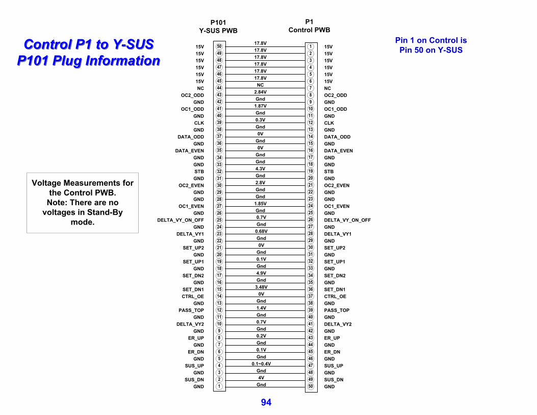
1 15V2 15V3 15V4 15V5 15V6 15V7 NC8 OC2_ODD9 GND
10
CLK11
GND12
DATA_ODD13
GND14
DATA_EVEN151617
STB18
GND1920
GNDGND
OC2_EVEN2122 GND
GND23OC1_EVEN24
DELTA_VY_ON_OFFGND25
GND26
DELTA_VY127
GND28
SET_UP229
GND30
SET_UP131
GND32
SET_DN2333435 GND
41 DELTA_VY242 GND43 ER_UP44 GND45 ER_DN46 GND47 SUS_UP484950 GND
SUS_DNGND
36 SET_DN137 CTRL_OE38 GND39 PASS_TOP40 GND
OC1_ODDGND
1234567891011121314151617181920212223242526272829303132333435
41424344454647484950
3637383940
15V15V15V15V15V15VNC
OC2_ODDGND
CLKGND
DATA_ODDGND
DATA_EVEN
STBGND
GNDGND
OC2_EVENGNDGND
OC1_EVEN
DELTA_VY_ON_OFFGND
GNDDELTA_VY1
GNDSET_UP2
GNDSET_UP1
GNDSET_DN2
GND
DELTA_VY2GND
ER_UPGND
ER_DNGND
SUS_UP
GNDSUS_DN
GND
SET_DN1CTRL_OE
GNDPASS_TOP
GND
OC1_ODDGND
P101Y-SUS PWB
P1Control PWB
17.8V17.8V17.8V17.8V17.8V17.8V
NC2.84VGnd
1.87VGnd0.3VGnd0V
Gnd0V
GndGnd4.3VGnd2.8VGndGnd
1.85VGnd0.7VGnd
0.68VGnd0V
Gnd0.1VGnd4.9VGnd
3.48V0V
Gnd1.4VGnd0.7VGnd0.2VGnd0.1VGnd
0.1~0.4VGnd4V
Gnd
Pin 1 on Control isPin 50 on Y-SUSControl P1 to Y-SUS
P101 Plug InformationControl P1 to Y-SUS
P101 Plug Information
94
Voltage Measurements for the Control PWB.
Note: There are no voltages in Stand-By
mode.

95 Fall 2009 1080P Plasma 50PS60
1.44V1.85VOC1_EVEN24
GndGndGND23
GndGndGND22
1.44V2.8VOC2_EVEN21
GndGndGND20
GndGndGND25
1.44V4.3VSTB19
GndGndGND18
GndGndGND17
1.44V0VDATA_EVEN16
GndGndGND15
1.44V0VDATA_ODD14
GndGndGND13
1.44V0.3VCLK12
GndGndGND11
1.44V1.87VOC1_ODD10
GndGndGND9
1.44V2.84VOC2_ODD8
NCNCNC7
Open17.8V15V6
Open17.8V15V5
Open17.8V15V4
Open17.8V15V3
Open17.8V15V2
Open17.8V15V1
Diode ModeRun LabelPin
1.44V0.1VER_DN45
GndGndGND46
1.44V0.1~0.4VSUS_UP47
GndGndGND48
1.44V4VSUS_DN49
GndGndGND50
GndGndGND44
1.44V0.2VER_UP43
GndGndGND42
1.44V0.7VDELTA_VY241
GndGndGND40
1.44V1.4VPASS_TOP39
GndGndGND38
1.44V0VCTRL_OE37
1.44V3.48VSET_DN136
GndGndGND35
1.44V4.9VSET_DN234
GndGndGND33
1.44V0.1VSET_UP132
GndGndGND31
1.44V0VSET_UP230
GndGndGND29
1.44V0.68VDELTA_VY128
GndGndGND27
1.44V0.7VDELTA_VY_ON_OFF26
Diode ModeRun LabelPin
Control P1 to YControl P1 to Y--SUS P101 Plug InformationSUS P101 Plug Information Pin 1 on Control is Pin 50 on Y-SUS.Note: There are no voltages in Stand-By mode

96 Fall 2009 1080P Plasma 50PS60
P101 Connector "Control BoardP101 Connector "Control Board”” to to ““Left X PWBLeft X PWB”” P110P110
0.97V1.27V24
0.97V1.0V26
0.97V1.27V27
0.97V1.0V28
0.97V1.27V29
0.97V1.0V31
0.97V1.0V23
0.97V1.0V20
0.97V1.27V21
0.97V1.0V18
0.97V1.27V19
0.97V1.0V15
0.97V1.27V16
0.97V1.27V32
0.97V1.27V14
0.97V1.0V13
0.97V1.27V12
0.97V1.0V11
0.97V1.27V9
0.97V1.0V8
0.97V1.27V7
0.97V1.0V6
0.67V3.3V1~4
Diode ModeRun Pin
Leave Connector P101 Connected to the X-Board P110
Pins with no TP are Gnd.
1~41~466
1111
2020
3131
4040
5656
0.97V1.0V53
0.97V1.27V54
1.2V1.87V56
1.2V1.87V57
1.2V3.22V58
1.1V0.49V59
0.97V1.27V52
0.97V1.27V50
0.97V1.0V51
0.97V1.27V47
0.97V1.0V49
0.97V1.27V45
0.97V1.0V46
1.1V0.49V60
0.97V1.0V44
0.97V1.27V42
0.97V1.0V41
0.97V1.27V40
0.97V1.0V39
0.97V1.27V37
0.97V1.0V36
0.97V1.27V34
0.97V1.0V33
Diode ModeRun Pin
1~4 pins 3.3V TP
50506060
5757
White hash White hash marks countmarks count
as 5as 5
5959
5858
Pin 1Pin 1

97 Fall 2009 1080P Plasma 50PS60
P102 Connector "Control BoardP102 Connector "Control Board”” to to ““Center X PWBCenter X PWB”” P210P210
0.97V1.27V19
0.97V1.0V18
0.97V1.27V16
0.97V1.0V15
0.97V1.27V13
0.97V1.0V12
0.97V1.27V10
0.97V1.0V9
0.97V1.27V7
0.97V1.0V6
0.67V3.3V1~4
Diode ModeRun Pin
Leave Connector P102 Connected to the Center X-Board P110
Note: There are no voltages in Stand-By mode.
Pins with no TP are Gnd.
0.97V1.27V21
0.97V1.0V22
0.97V1.0V33
0.97V1.27V34
0.97V1.0V36
0.97V1.27V31
0.97V1.0V30
0.97V1.27V28
0.97V1.0V27
0.97V1.27V25
0.97V1.0V24
Diode ModeRun Pin
0.97V1.27V37
0.97V1.0V39
0.97V1.27V40
0.97V1.0V42
0.97V1.27V46
0.97V1.0V48
0.97V1.27V49
0.97V1.0V51
0.97V1.27V52
0.97V1.0V45
0.97V1.27V43
Diode ModeRun Pin
0.97V1.0V53
0.97V1.27V54
1.2V1.0V56
1.2V1.27V57
1.2V1.0V58
1.1V1.27V59
1.1V1.0V60
Diode ModeRun Pin
1~41~4
66
1010 3030 4040 60603.3V TP1ST 4 pins
56562121
5151
White hash White hash marks countmarks count
as 5as 5
Pin 1Pin 1

98 Fall 2009 1080P Plasma 50PS60
P104 Connector "Control BoardP104 Connector "Control Board”” to to ““Right X PWBRight X PWB”” P310P310
0.98V1.27V24
0.98V1.0V26
0.98V1.27V27
0.98V1.0V28
0.98V1.27V29
0.98V1.0V31
0.98V1.0V23
0.98V1.0V20
0.98V1.27V21
0.98V1.0V18
0.98V1.27V19
0.98V1.0V15
0.98V1.27V16
0.98V1.27V32
0.98V1.27V14
0.98V1.0V13
0.98V1.27V12
0.98V1.0V11
0.98V1.27V9
0.98V1.0V8
0.98V1.27V7
0.98V1.0V6
0.67V3.3V1~4
Diode ModeRun Pin
1~41~466
1010
2020
4040
5656
Leave Connector P104 Connected to the X-Board P310
Note: There are no voltages in Stand-By mode. Pins with no TP are Gnd.
6060
0.98V1.0V53
0.98V1.27V54
0.49V1.87V56
0.49V1.87V57
3.22V3.22V58
1.87V0.49V59
0.98V1.27V52
0.98V1.27V50
0.98V1.0V51
0.98V1.27V47
0.98V1.0V49
0.98V1.27V45
0.98V1.0V46
1.87V0.49V60
0.98V1.0V44
0.98V1.27V42
0.98V1.0V41
0.98V1.27V40
0.98V1.0V39
0.98V1.27V37
0.98V1.0V36
0.98V1.27V34
0.98V1.0V33
Diode ModeRun Pin
3.3V TP
3131
5050
White hash White hash marks countmarks count
as 5as 5
Pin 1Pin 1

99 Fall 2009 1080P Plasma 50PS60
X BOARD (LEFT, RIGHT and CENTER) SECTIONX BOARD (LEFT, RIGHT and CENTER) SECTION
The following section gives detailed information about the X boaThe following section gives detailed information about the X boards. rds. These boards deliver the Color information signal developed on tThese boards deliver the Color information signal developed on the he Control board to the TCPs, (Taped Carrier Packages). The TCPs arControl board to the TCPs, (Taped Carrier Packages). The TCPs are e attached to the vertical FPCs, (Flexible Printed Circuits) whichattached to the vertical FPCs, (Flexible Printed Circuits) which are are attached directly to the panel. The X boards are the attachment attached directly to the panel. The X boards are the attachment points for these FPCs.points for these FPCs.These boards have no adjustment. These boards have no adjustment.
These boards receive their main B+ from the:These boards receive their main B+ from the:
•• Originally developed on the Switched Mode Power Supply Originally developed on the Switched Mode Power Supply Va (Voltage for Address) is routed through the YVa (Voltage for Address) is routed through the Y--SUS board SUS board and then to the Left X board via P121 pins 1~4. Va also and then to the Left X board via P121 pins 1~4. Va also leaves P120 and is sent to the Center X via P220. Then it leaves P120 and is sent to the Center X via P220. Then it leaves on P221 and goes to the Right X P320.leaves on P221 and goes to the Right X P320.
•• Control board develops 3.3V and routes to each X board via Control board develops 3.3V and routes to each X board via ribbon connectors P110, P210 and P310.ribbon connectors P110, P210 and P310.

100 Fall 2009 1080P Plasma 50PS60
X PWB Additional InformationX PWB Additional Information
There are three X boards, the Left, Center and the Right There are three X boards, the Left, Center and the Right (As viewed from the rear of the set).(As viewed from the rear of the set).
The three X boards have very little circuitry. They are basicallThe three X boards have very little circuitry. They are basically signal y signal and voltage routing boards. and voltage routing boards.
•• They route the Va to all of the Taped Carrier Packages (TCPs).They route the Va to all of the Taped Carrier Packages (TCPs).Va is introduced to the Left X board first, then the Left X sVa is introduced to the Left X board first, then the Left X sends ends Va to the Center X and then the Center X sends Va to the RighVa to the Center X and then the Center X sends Va to the Right X.t X.
•• They route the Logic (Color) signals from the Control board They route the Logic (Color) signals from the Control board to all of the Taped Carrier Packages (TCPs). Including to all of the Taped Carrier Packages (TCPs). Including VPPVPP which is which is generated on each of the 3 X boards.generated on each of the 3 X boards.
The X boards have connectors to 23 TCPs, 8 on the left and rightThe X boards have connectors to 23 TCPs, 8 on the left and right and and 7 on the center. The Center X board has connections to 7 TCPs.7 on the center. The Center X board has connections to 7 TCPs.
There are a total of 23 TCPs and each TCP has 2 buffers. So therThere are a total of 23 TCPs and each TCP has 2 buffers. So there e are a total of 46 buffers feeding the panelare a total of 46 buffers feeding the panel’’s 5760 vertical electrodes.s 5760 vertical electrodes.

101 Fall 2009 1080P Plasma 50PS60
X PWB TCP Heat Sink WarningX PWB TCP Heat Sink Warning
The Vertical The Vertical Address buffers Address buffers (TCPs) have one (TCPs) have one heat sink across heat sink across
all 23 TCPs as all 23 TCPs as indicated by the indicated by the
arrow.arrow.
NEVER run the television with this heat sink removed. NEVER run the television with this heat sink removed. Damage to the TCPs will occur and cause a defective panel.Damage to the TCPs will occur and cause a defective panel.

102 Fall 2009 1080P Plasma 50PS60
X PWB Layout Primary Circuit Diode CheckX PWB Layout Primary Circuit Diode CheckThe three X-Boards have two similar circuit layouts for the connections going to the TCPs., as shown below.
On any Va (0.54V) TCPs connected.On any Va (0.84V) TCPs disconnected.On 3.3V (0.42V)On any VPP (0.42V)
On any Gnd+
- On the below:
On any Va (Open)On 3.3V (0.62V)On any VPP (Open)
On any Gnd-
+ On the below:
Readings given with TCPs connected unless specified.

103 Fall 2009 1080P Plasma 50PS60
TCPAttached directly to Flexible cable
Connector
Fram
e
X_B/D
Front panel H
orizontal A
dd
ressRear pa
nel Vertical A
dd
ress
TCP (Tape Carrier Package)TCP (Tape Carrier Package)
Control Board
Back side of TCP Ribbon
TCP
Taped Carrier Package
Flexible Cable
Y-SUS BoardVa
Logic
Connector
X Drive Board
Heat Sink
128 lines 128 lines
256 total lines
This shows the layout of the bottom ribbon cables connecting to the Panel’s Vertical electrodes, (Address Bus). Note that each ribbon cable has a solid state device called a TCP attached.
256 VerticalElectrodes
Chocolate

104 Fall 2009 1080P Plasma 50PS60
TCP TestingTCP Testing
Look for any TCPs being discolored.Ribbon Damage. Cracks, folds Pinches, scratches, etc…
On any Gnd
On any Va (0.58V)On 3.3V (0.72V)On any VPP (0.58V)
-
+
Reverse leads reads Open10 15 20 25 30 35 40 45 501
Va VaGnd
GndVPP VPP3.3VGnd
Must be checked on flexible cable.
On the below:
5

105 Fall 2009 1080P Plasma 50PS60
TCP 3.3V B+ CheckTCP 3.3V B+ Check Warning: DO NOT attempt to run the set with the Heat Sink over the TCPs removed.
Checking IC304 for 3.3V, use center pin.
IC3040V
3.3V5V
3.3V in on Pins 57 ~ 60 on any connector
Left X PWB P110 Right X PWB P310Center X PWB P210
For Connectors P101, P102 and P104 on the Control board, see Control board section.
3.3V for TCPsIC304 on
Control Board
All Connectors to All TCPs look very similar for the 3.3V test point. The upside down L trace at pins 34 and 35 of each connector. Example here from P204. You can only check for continuity, you can not run the set with heat sink removed.
Red Lead On 3.3V (0.42V)Black Lead On 3.3V (0.62V)This also test IC100, IC200 and IC300

106 Fall 2009 1080P Plasma 50PS60
TCP Visual Observation. Damaged TCPTCP Visual Observation. Damaged TCP
This damaged TCP can,a) Cause the Power Supply to shutdownb) Generate abnormal vertical barsc) Cause the entire area driven by the TCP to be “All White”d) Cause the entire area driven by the TCP to be “All Black”e) Cause a “Single Line” defect
Warning: DO NOT attempt to run the set with the Heat Sink over the TCPs removed. After a very short time, these ICs will begin to self destruct due to overheating.

107 Fall 2009 1080P Plasma 50PS60
Diode Mode Readings taken with all connectors Disconnected. Black lead on Gnd. DVM in Diode Mode.
Left X Drive P121 Connector to YLeft X Drive P121 Connector to Y--SUS P307 InformationSUS P307 Information
GndGndGnd7GndGndGnd6NCNCNC5
Open*65VVA4Open*65VVA3Open*65VVA2Open*65VVA1
Diode ModeRun LabelPin
* Note: This voltage will vary in accordance with Panel Label
P121 CONNECTOR " X-Drive Left PWB" to "Y-SUS” P307
Voltage and Diode Mode Measurement (No Stand-By Voltages)
1

108 Fall 2009 1080P Plasma 50PS60
P110 Connector P110 Connector ““Left X PWBLeft X PWB”” to to ““ControlControl”” P101P101
0.97V1.0V28
0.97V1.27V27
0.97V1.0V25
0.97V1.27V24
0.97V1.0V22
0.97V1.27V21
0.97V1.0V20
0.97V1.27V19
0.97V1.0V17
0.97V1.27V16
0.97V1.0V15
0.97V1.27V14
0.97V1.0V12
0.97V1.27V11
0.97V1.0V10
0.97V1.27V9
0.97V1.0V8
0.97V1.27V7
1.2V1.87V5
1.21.87V4
1.2V3.22V3
1.1V0.49V2
1.1V0.49V1
Diode ModeRun Pin
Leave Connector P310 Connected to the Control Board P104
0.67V3.3V57~60
0.97V1.0V55
0.97V1.27V54
0.97V1.0V53
0.97V1.27V52
0.97V1.0V50
0.97V1.27V49
0.97V1.0V48
0.97V1.27V47
0.97V1.0V46
0.97V1.27V45
0.97V1.0V43
0.97V1.27V42
0.97V1.0V41
0.97V1.27V40
0.97V1.0V38
0.97V1.27V37
0.97V1.0V35
0.97V1.27V34
0.97V1.0V33
0.97V1.27V32
0.97V1.0V30
0.97V1.27V29
Diode ModeRun Pin
Pins with no TP are Gnd.
57~6057~60 11
57~60 pins 3.3V TP
White hash marks White hash marks count as 5count as 5
Pin 1Pin 11515
n/c56
Gnd6
Gnd11
Gnd14
Gnd19
Gnd22
Gnd27
Gnd32
Gnd35
Gnd38
Gnd41
Gnd44
Gnd47
Gnd50
Gnd53

109 Fall 2009 1080P Plasma 50PS60
P210 Connector "Center X PWBP210 Connector "Center X PWB““ to to ””Control BoardControl Board”” P102P102
0.97V1.0V28
0.97V1.27V27
0.97V1.0V25
0.97V1.27V24
0.97V1.0V22
0.97V1.27V21
0.97V1.0V20
0.97V1.27V19
0.97V1.0V17
0.97V1.27V16
0.97V1.0V15
0.97V1.27V14
0.97V1.0V12
0.97V1.27V11
0.97V1.0V10
0.97V1.27V9
0.97V1.0V8
0.97V1.27V7
1.2V1.87V5
1.21.87V4
1.2V3.22V3
1.1V0.49V2
1.1V0.49V1
Diode ModeRun Pin
Leave Connector P210 Connected to the Control Board P102
0.67V3.3V57~60
0.97V1.0V55
0.97V1.27V54
0.97V1.0V53
0.97V1.27V52
0.97V1.0V50
0.97V1.27V49
0.97V1.0V48
0.97V1.27V47
0.97V1.0V46
0.97V1.27V45
0.97V1.0V43
0.97V1.27V42
0.97V1.0V41
0.97V1.27V40
0.97V1.0V38
0.97V1.27V37
0.97V1.0V35
0.97V1.27V34
0.97V1.0V33
0.97V1.27V32
0.97V1.0V30
0.97V1.27V29
Diode ModeRun Pin
Pins with no TP are Gnd.
57~6057~60
11
57~60 pins 3.3V TP
White hash marks White hash marks count as 5count as 5
Pin 1Pin 11515
n/c56
Gnd6
Gnd13
Gnd18
Gnd23
Gnd26
Gnd31
Gnd36
Gnd39
Gnd44
Gnd51

110 Fall 2009 1080P Plasma 50PS60
P310 Connector P310 Connector ““Right X BoardRight X Board”” to to ““ControlControl”” P104P104Leave Connector P310 Connected to the Control Board P104
Pins with no TP are Gnd.
57~6057~6011
57~60 pins 3.3V TP
White hash marks White hash marks count as 5count as 5
Pin 1Pin 11515
0.97V1.0V28
0.97V1.27V27
0.97V1.0V25
0.97V1.27V24
0.97V1.0V22
0.97V1.27V21
0.97V1.0V20
0.97V1.27V19
0.97V1.0V17
0.97V1.27V16
0.97V1.0V15
0.97V1.27V14
0.97V1.0V12
0.97V1.27V11
0.97V1.0V10
0.97V1.27V9
0.97V1.0V8
0.97V1.27V7
1.2V1.87V5
1.21.87V4
1.2V3.22V3
1.1V0.49V2
1.1V0.49V1
Diode ModeRun Pin
0.67V3.3V57~60
0.97V1.0V55
0.97V1.27V54
0.97V1.0V53
0.97V1.27V52
0.97V1.0V50
0.97V1.27V49
0.97V1.0V48
0.97V1.27V47
0.97V1.0V46
0.97V1.27V45
0.97V1.0V43
0.97V1.27V42
0.97V1.0V41
0.97V1.27V40
0.97V1.0V38
0.97V1.27V37
0.97V1.0V35
0.97V1.27V34
0.97V1.0V33
0.97V1.27V32
0.97V1.0V30
0.97V1.27V29
Diode ModeRun Pin
n/c56
Gnd6
Gnd13
Gnd18
Gnd23
Gnd26
Gnd31
Gnd36
Gnd39
Gnd44
Gnd51

111 Fall 2009 1080P Plasma 50PS60
P120, P220, P221 and P320 X Board Connector Information (Va distP120, P220, P221 and P320 X Board Connector Information (Va distribution)ribution)White hash marks count as 5White hash marks count as 5
1~121~12VaVa
19~3019~30VaVa
P120 P220Left X Center X Center X Right X
P221 P320
16~18 16~18 ncnc
On any Va (0.54V) TCPs connected.On any Va (0.84V) TCPs disconnected.
On any Gnd+
- On any Va (Open)TCPs connectedor disconnected
On any Gnd-
+Note: Va voltage will vary by panel, check your specific panelNote: Va voltage will vary by panel, check your specific panel’’s voltage label.s voltage label.
1~15 1~15 GndGnd
16~30 16~30 GndGnd
13~15 13~15 ncnc
1~121~12VaVa
19~3019~30VaVa
16~18 16~18 ncnc
1~15 1~15 GndGnd
16~30 16~30 GndGnd
13~15 13~15 ncnc

112 Fall 2009 1080P Plasma 50PS60
MAIN PWB SECTIONMAIN PWB SECTIONThe following section gives detailed information about the Main The following section gives detailed information about the Main board. This board. This board contains the Microprocessor, Audio section, video section board contains the Microprocessor, Audio section, video section and all and all input, outputs. It also receives all input signals and processesinput, outputs. It also receives all input signals and processes them to be them to be delivered to the Control board via the LVDS cable. The main tunedelivered to the Control board via the LVDS cable. The main tuner (r (VSBVSB, , 8VSB and QAM) is located on the main board. This board is also w8VSB and QAM) is located on the main board. This board is also where the here the televisiontelevision’’s software upgrades are accomplished through the USB input.s software upgrades are accomplished through the USB input.
This board has no adjustment. This board has no adjustment.
The Main Board Receives its operational voltage from the SMPS:The Main Board Receives its operational voltage from the SMPS:
•• STBY 5VSTBY 5V
•• +5V from the Switched Mode Power Supply+5V from the Switched Mode Power Supply
•• 12V for Tuner (Stepped down to 5V)12V for Tuner (Stepped down to 5V)
•• 17V for Audio17V for Audio
DURING STAND BY 5V:DURING STAND BY 5V:
DURING RUN: (STBY 5V remains)DURING RUN: (STBY 5V remains)

113 Fall 2009 1080P Plasma 50PS60
TunerComponent inputs
LVDS (Video)To Control
RGB/PC
P1006
P1001
P1005
AVIn 3
To Power Supply
HDMI inputs
RS232
SPK Out
To Front
Controls
Main PWB Layout and IdentificationMain PWB Layout and Identification
X112 Mhz
Audio
Audio RGB/DVI
USB
HDMI 3
Wired Remote
A/V Composite inputs
P1003
Pin 1
LD501
Pin 19
S-In
RF
OpticalAudio
IC801
IC504
IC952
IC804
IC1Micro
Tuner X501
25 Mhz
IC302
IC503
IC1001
IC203
IC805
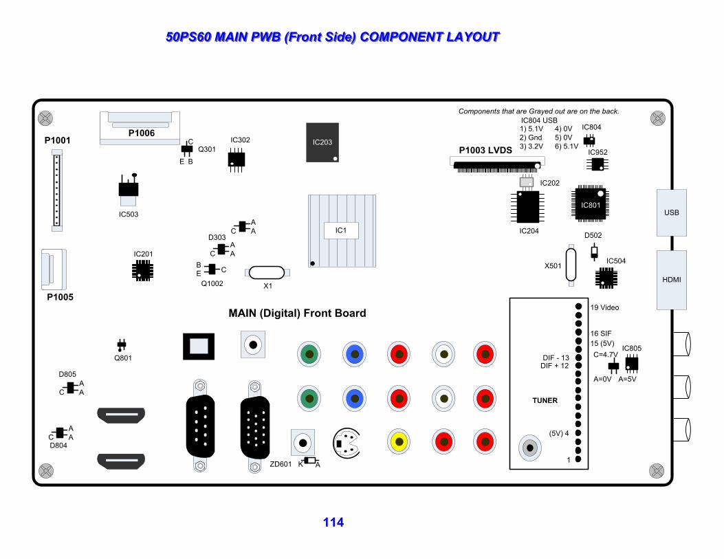
50PS60 MAIN PWB (Front Side) COMPONENT LAYOUT50PS60 MAIN PWB (Front Side) COMPONENT LAYOUT
114
MAIN (Digital) Front Board
1
TUNER
16 SIF
19 Video
(5V) 4
DIF + 12DIF - 13
15 (5V)
D502
IC952
IC804
Components that are Grayed out are on the back.
IC302
IC503
X1
X501IC201
P1006
P1003 LVDSP1001
P1005
IC1
IC801
IC504
HDMI
USB
IC805
A=5VA=0V
C=4.7V
D303
Q1002
IC203
D805
D804
Q801
K AZD601
IC202
IC204
Q301
1) 5.1V2) Gnd3) 3.2V
4) 0V5) 0V6) 5.1V
IC804 USB
ACA
ACA
ACA
ACA
B CE
B
C
E

115 Fall 2009 1080P Plasma 50PS60
Main PWB Back Side (Regulator Checks)Main PWB Back Side (Regulator Checks)
IC305
IC502
IC304
IC201
IC601
IC803
IC802IC602
D951
D801
Q951
Q502
Q503
Q504
Q501
IC301
Q303
Q302
Q1001
D892
D802
D890
IC202
IC505
D1001
D628
Q602 D627

50PS60 MAIN PWB COMPONENT LAYOUT
116
31 2
2
Q305
MAIN (Digital) Front Board
1
TUNER
16 SIF
19 Video
(5V) 4
DIF + 12DIF - 13
15 (5V)
D502
IC952
IC804
Components that are Grayed out are on the back.
IC302
IC503
X1
X501
IC505
IC201
P1006
P1003 LVDSP1001
P1005
IC1
IC801
IC504
HDMI
USB
IC805
A=5VA=0V
C=4.7V
D303
Q1002
Q303
IC203
D805
D804
Q801
K AZD601
D951
IC202
IC304
IC201
21 3
2
D801
B
C
E
B
C
E
B
C
E
Q951
Q891
Q503
C A
D1001
Q302
Q1001
IC601
A
K
AD802
IC803
IC802
Q892
A
K
AD628
Q601D627
A
K
AB
C
EQ890
B
C
E
B
C
E
IC602
A
K
A
Q502
B
C
E
IC204
IC301
Q301
B
C
E
B
C
E
B
C
E
B CE
B
C
E
ACA
ACA
ACA
A
C
AA
C
A
D633
2
3
1 1) 5.1V2) Gnd3) 3.2V
4) 0V5) 0V6) 5.1V
IC804 USB
IC502Q504
Q501C
B E
GndOut
In
Out
D
G S
2
321
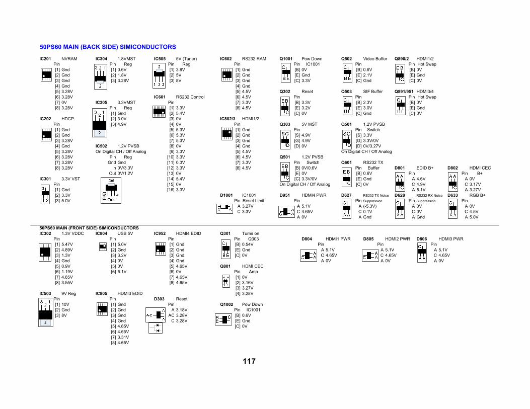
50PS60 MAIN (BACK SIDE) SIMICONDUCTORS
IC201 NVRAM IC304 1.8VMST IC505 5V (Tuner) IC602 RS232 RAM Q1001 Pow Down Q502 Video Buffer Q890/2 HDMI1/2Pin Pin Reg Pin Reg Pin Pin IC1001 Pin Pin Hot Swap[1] Gnd [1] 0.6V [1] 3.8V [1] Gnd [B] 0V [B] 0.6V [B] 0V[2] Gnd [2] 1.8V [2] 5V [2] Gnd [E] Gnd [E] 2.1V [E] Gnd[3] Gnd [3] 3.28V [3] 8V [3] Gnd [C] 3.3V [C] Gnd [C] 0V[4] Gnd [4] Gnd[5] 3.28V [5] 4.5V Q302 Reset Q503 SIF Buffer Q891/951 HDMI3/4[6] 3.28V IC601 RS232 Control [6] 4.5V Pin Pin Pin Hot Swap[7] 0V IC305 3.3VMST Pin [7] 3.3V [B] 3.3V [B] 2.3V [B] 0V[8] 3.28V Pin Reg [1] 3.3V [8] 4.5V [E] 3.2V [E] 3.0V [E] Gnd
[1] Gnd [2] 5.4V [C] 0V [C] Gnd [C] 0VIC202 HDCP [2] 3.0V [3] 0V IC802/3 HDMI1/2
Pin [3] 4.9V [4] 0V Pin Q303 5V MST Q501 1.2V PVSB[1] Gnd [5] 5.3V [1] Gnd Pin Pin Switch[2] Gnd [6] 5.3V [2] Gnd [S] 4.9V [S] 3.3V[3] 3.28V [7] 5.3V [3] Gnd [G] 4.9V [G] 3.3V/0V[4] Gnd IC502 1.2V PVSB [8] 0V [4] Gnd [D] 0V [D] 0V/3.27V[5] 3.28V On Digital CH / Off Analog [9] 3.3V [5] 4.5V On Digital CH / Off Analog[6] 3.28V Pin Reg [10] 3.3V [6] 4.5V Q501 1.2V PVSB[7] 3.28V Gnd Gnd [11] 0.3V [7] 3.3V Pin Switch Q601 RS232 TX[8] 3.28V In 0V/3.3V [12] 3.3V [8] 4.5V [B] 0V/0.6V Pin Buffer D801 EDID B+ D802 HDMI CEC
Out 0V/1.2V [13] 0V [E] 0V [B] 0.6V Pin Pin B+IC301 3.3V VST [14] 5.4V [C] 3.3V/0V [E] Gnd A 4.6V A 0V
Pin [15] 0V On Digital CH / Off Analog [C] 0V C 4.9V C 3.17V[1] Gnd [16] 3.3V A 5.1V A 3.27V[2] 3.3V D1001 IC1001 D951 HDMI4 PWR D627 RS232 TX Noise D628 RS232 RX Noise D633 RGB B+[3] 5.0V Pin Reset Limit Pin Pin Suppression Pin Suppression Pin
A 3.27V A 5.1V A (-5.3V) A 0V A 0VC 3.3V C 4.65V C 0.1V C 0V C 4.5V
A 0V A Gnd A Gnd A 5.0V
50PS60 MAIN (FRONT SIDE) SIMICONDUCTORSIC302 1.3V VDDC IC804 USB 5V IC952 HDMI4 EDID Q301 Turns on
Pin Pin Pin Pin Q303 D804 HDMI1 PWR D805 HDMI2 PWR D806 HDMI3 PWR[1] 5.47V [1] 5.0V [1] Gnd [B] 0.54V Pin Pin Pin[2] 4.89V [2] Gnd [2] Gnd [E] Gnd A 5.1V A 5.1V A 5.1V[3] 1.3V [3] 3.2V [3] Gnd [C] 0V C 4.65V C 4.65V C 4.65V[4] Gnd [4] 0V [4] Gnd A 0V A 0V A 0V[5] 0.9V [5] 0V [5] 4.65V Q801 HDMI CEC[6] 1.19V [6] 5.1V [6] 0V Pin Amp[7] 4.85V [7] 4.65V [1] 0V[8] 3.55V [8] 4.65V [2] 3.16V
[3] 3.27VIC503 9V Reg IC805 HDMI3 EDID [4] 3.28V
Pin Pin D303 Reset[1] 10V [1] Gnd Pin Q1002 Pow Down[2] Gnd [2] Gnd A 3.18V Pin IC1001[3] 8V [3] Gnd AC 3.28V [B] 0.6V
[4] Gnd C 3.28V [E] Gnd[5] 4.65V [C] 0V[6] 4.65V[7] 3.31V[8] 4.65V
117

118 Fall 2009 1080P Plasma 50PS60
Main PWB Tuner Check (Shield Off) Pins Exposed TDVWMain PWB Tuner Check (Shield Off) Pins Exposed TDVW--H103FH103F
Video Pin 19 Video Test Point
SIF Pin 16 Audio Test Point
Pin 4 Tuner B+ (5V)
Pin 1 n/c
DIG IF (-) Pin 13DIG IF (+) Pin 12Digital Channel Test Point
Data Pin 9Clock Pin 8
TU501
MAIN PWB
Tuner Location

119 Fall 2009 1080P Plasma 50PS60
MAIN PWB
Main PWB Tuner Video Main PWB Tuner Video and SIF Output Checkand SIF Output Check
Tuner Location
Pin 19 “Video”Signal
Pin 16 “SIF”Signal
USING COLOR BAR SIGNAL INPUT
Pin 12 and Pin 13“Dig IF” Signal
Note: 8VSB or QAM Only“Dig IF” Signal only when receiving a Digital Channel.
Pin 1
Note: NTSC Only“Video Out” Signal only when receiving an analog Channel.
100mV / 1uSec
700mVp/p
450mVp/p
200mV / 2uSec
2.24Vp/p
500mV / 10uSec
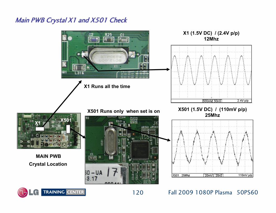
120 Fall 2009 1080P Plasma 50PS60
MAIN PWB
Main PWB Crystal X1 and X501 CheckMain PWB Crystal X1 and X501 Check
Crystal Location
X1 (1.5V DC) / (2.4V p/p)12Mhz
X501 (1.5V DC) / (110mV p/p)25Mhz
X1 Runs all the time
X1 X501
X501 Runs only when set is on

121 Fall 2009 1080P Plasma 50PS60
Main PWB P1003 (Removing the LVDS CableMain PWB P1003 (Removing the LVDS Cable
(1) Using your fingernail, lift up the locking mechanism.(1) Using your fingernail, lift up the locking mechanism.
Since the locking tab is very thin and fragile, its best to liftSince the locking tab is very thin and fragile, its best to liftslightly one end, then work across the locking tabslightly one end, then work across the locking taba little at a time, back and forth until the tab is released.a little at a time, back and forth until the tab is released.
(2) Pull the Cable from the Connector(2) Pull the Cable from the Connector

122 Fall 2009 1080P Plasma 50PS60
MAIN PWB
Main PWB P1003 LVDS Video Signal Test PointsMain PWB P1003 LVDS Video Signal Test Points
P1003 Location
Pin
3939
1111
3636
1212
4040
3030
1717
1313
14141616 1919
3838
37373535
3333
32322929
2828
2727 2424
2323
2020
2222
2121
LVDS Waveform TPs
P1003 Location
TP Locations

123 Fall 2009 1080P Plasma 50PS60
Main PWB P203 LVDS Video Signal CheckMain PWB P203 LVDS Video Signal CheckPins 11, 12, 16 and 17Pins 11, 12, 16 and 17
SMTP Color Bar Signal Input
Waveform TP see 1 page back
Pin 17 (R1020) Pin 16 (R1019)
Pin 12 (R1024) Pin 11 (R1023)
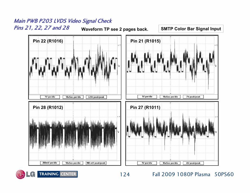
124 Fall 2009 1080P Plasma 50PS60
Main PWB P203 LVDS Video Signal CheckMain PWB P203 LVDS Video Signal CheckPins 21, 22, 27 and 28Pins 21, 22, 27 and 28 SMTP Color Bar Signal InputWaveform TP see 2 pages back.
Pin 28 (R1012) Pin 27 (R1011)
Pin 22 (R1016) Pin 21 (R1015)
125 Fall 2009 1080P Plasma 50PS60
Voltage and Diode Test for the Main Board
Diode Mode Check with the PWB Disconnected.
Main PWB Plug P1003 Main PWB Plug P1003 ““LVDSLVDS”” VoltagesVoltages
0.8V1.2V0VRB2-29
0.9V1.45V0VRA2+28
RA2-
RE1+
RE1-
RD1+
RD1-
RCLK1+
RCLK1-
RC1+
RC1-
RB1+
RB1-
RA1+
RA1-
Label
0.9V1.0V0V27
0.7V1.24V0V24
0.9V1.26V0V23
0.9V1.18V0V22
0.9V1.26V0V21
0.9V1.23V0V20
0.88V0V0V19
0.84V1.20V0V17
0.94V1.27VV0V16
0.94V0V0V14
0.84V1.29V0V13
0.94V1.19V0V12
0.89V1.46V0V11
Diode ModeRunSBYPin
P1003 CONNECTOR "Main" to P121 "Control PWB"
Open0.5V0VROM-RX150
ROM-TX1
SCL
DISP-EN
SDA
RE2+
RE2-
RD2+
RD2-
RCLK2+
RCLK2-
RC2+
RC2-
RB2+
Label
Open3.28V0V49
Open3.28V0V48
0.5V2.8V0V47
Open3.28V0V46
0.9V1.3V0V40
0.9V1.18V0V39
0.9V1.29V0V38
0.9V1.16V0V37
0.9V1.26V0V36
0.9V1.22V0V35
0.9V1.20V0V33
0.8V1.27V0V32
0.7V1.26V0V30
Diode ModeRunSBYPin
P1003 CONNECTOR "Main" to P121 "Control PWB"
NOTE: This is a 51 pin connector. Pins 6-8, 15, 31, 34, 41 and 51 are Ground (Gnd). Pins 1-5, 9-10, 25-26, 42-45 are No Connection (n/c).
Pin
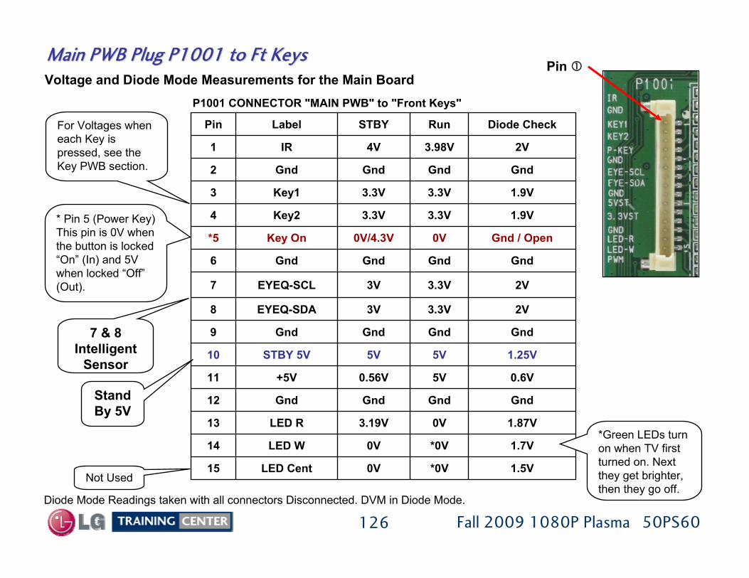
126 Fall 2009 1080P Plasma 50PS60
Voltage and Diode Mode Measurements for the Main Board
Diode Mode Readings taken with all connectors Disconnected. DVM in Diode Mode.
Main PWB Plug P1001 to Ft Keys Main PWB Plug P1001 to Ft Keys
P1001 CONNECTOR "MAIN PWB" to "Front Keys"
Pin
1.5V*0V0VLED Cent15
1.7V*0V0VLED W14
1.87V0V3.19VLED R13
GndGndGndGnd12
0.6V5V0.56V+5V11
1.25V5V5VSTBY 5V10
GndGndGndGnd9
2V3.3V3VEYEQ-SDA8
2V3.3V3VEYEQ-SCL7
GndGndGndGnd6
Gnd / Open0V0V/4.3VKey On*5
1.9V3.3V3.3VKey24
1.9V3.3V3.3VKey13
GndGndGndGnd2
2V3.98V4VIR1
Diode CheckRun STBYLabelPin
Stand By 5V
Not Used
7 & 8Intelligent
Sensor
* Pin 5 (Power Key) This pin is 0V when the button is locked “On” (In) and 5V when locked “Off”(Out).
*Green LEDs turn on when TV first turned on. Next they get brighter, then they go off.
For Voltages when each Key is pressed, see the Key PWB section.

127 Fall 2009 1080P Plasma 50PS60
Main PWB Plug P1006 to Power Supply Voltages and Diode CheckMain PWB Plug P1006 to Power Supply Voltages and Diode CheckDiode Mode Check with the PWB Disconnected. DVM in the Diode mode.
Open3.3V0VM5 ON21
1.3V5V5VStby 5V23
Open3.3V0VRL On19
Open4.8V0V5V Det17*
GndGndGndGnd15
GndGndGndGnd13
1.0 V5.15V5.15VStby 5V11
1.0 V5.15V0V+5V9
GndGndGndGnd7
Open12V0V12V5
GndGndGndGnd3
Open17.3V0V17V1*
Diode ModeRun STBYLabelPin
P1006
Pin front
GndGndGndAuto Gnd22
Open*0V*0VKey On24*
Open3.2V0VVS On20
Open5V5VAC Det18*
Gndn/cn/cn/c16
GndGndGndGnd14
1.0 V5.15V0V+5V12
1.0 V5.15V0V+5V10
GndGndGndGnd8
Open12V0V12V6
GndGndGndGnd4
Open17.3V0V17V2*
Diode ModeRun STBYLabelPin
P1006 CONNECTOR "Main" to "SMPS PWB" P813
* Pin 24: When the Power Button is opened, • Pin 24 pulls up to 4.3V.• Stand-By 5V turns off. AC-Det remains.
* Pin 18: AC DET if missing will cause the set to turn off after 10 seconds.
* Pin 17: 5V Det not used.
* Pin 1 and 2: 17V If Vs is unloaded will pulsate.Turned on by Vs On Command.
* Pins 9, 10, 12: (+5V) Turned on by Relay On Command.

128 Fall 2009 1080P Plasma 50PS60
Voltage and Diode Mode Measurements for the Main Board Speaker Plug
Main PWB Speaker Plug P1005 Main PWB Speaker Plug P1005
P1005Speaker
Connector
Diode Mode Check with the PWB Disconnected. DVM in the Diode mode.
L+
L-
R+
R-
Label
Open8.65V0V4
Open8.65V0V3
Open8.65V0V2
Open8.65V0V1
Diode ModeRunSBYPin
MAIN PWB
Board Location
P1005 CONNECTOR "Main" to "Speakers"
Right (-)Right (+)
Left (-)Left (+)

129 Fall 2009 1080P Plasma 50PS60
FRONT IR, POWER LED and SIDE KEY PWB SECTIONFRONT IR, POWER LED and SIDE KEY PWB SECTION
The following section gives detailed information about the FrontThe following section gives detailed information about the Front IR, IR, Power LED and Side Key PWBs. These boards contains the Infrared Power LED and Side Key PWBs. These boards contains the Infrared Receiver, Intelligent Sensor, Side Keys and Power LEDs section.Receiver, Intelligent Sensor, Side Keys and Power LEDs section.The front Intelligent Sensor IC communicates with the Main PWB The front Intelligent Sensor IC communicates with the Main PWB Microprocessor via Clock and Data lines.Microprocessor via Clock and Data lines.
These boards have no adjustments. These boards have no adjustments.
The Front Control Board (IR and Intelligent Sensor) receives itsThe Front Control Board (IR and Intelligent Sensor) receives its main main B+ from the Main PWB:B+ from the Main PWB:
•• STBY 5V from the Main PWB. This voltage is originated on the STBY 5V from the Main PWB. This voltage is originated on the Switched Mode Power SupplySwitched Mode Power Supply
•• 3.3V generated on the Main PWB.3.3V generated on the Main PWB.
•• The Front Power LEDs are driven by 2 separate pins from the The Front Power LEDs are driven by 2 separate pins from the Main board.Main board.
130 Fall 2009 1080P Plasma 50PS60
Front Control (IR and Intelligent Sensor) PWB and Power LED PWB Front Control (IR and Intelligent Sensor) PWB and Power LED PWB LocationLocation
Lower Left Side (As viewed from rear).Lower Left Side (As viewed from rear).
Power LED PWB
Front IR PWB
131 Fall 2009 1080P Plasma 50PS60
Front Power LED and IR Board LayoutFront Power LED and IR Board Layout
Power LED PWB
Front IR PWB P2
P1
J1
J2
Intelligent Sensor
IRSensor
PowerLEDs
Ground snap

132 Fall 2009 1080P Plasma 50PS60
Front Power LED and IR Board Connector LayoutFront Power LED and IR Board Connector Layout
Front IR PWB
J1 J2
Power LEDPWB front
P2
P1
PowerLEDs
Power LEDPWB back
GreenRed (Stand-By)Green
Green LEDs turn on when power first turned on. Then they get brighter, then they go off.
J1 To PowerLED P2
J2 To SideKey P1
P1 To MainPWB P1001
P2 ToFt IR J1

133 Fall 2009 1080P Plasma 50PS60
Front IR and Intelligent Sensor Board LayoutFront IR and Intelligent Sensor Board Layout
Intelligent Sensor
U2
Infrared Sensor
U1
Ft View
U1

134 Fall 2009 1080P Plasma 50PS60
Front Control PWB Connector P1 Voltage and Pin IdentificationFront Control PWB Connector P1 Voltage and Pin IdentificationP1 CONNECTOR " Front Control PWB" to P1001 "Main PWB"
Diode Mode Readings taken with all connectors Disconnected. Black lead on Gnd. DVM in Diode Mode.
1
P1
1.5V*0V0VLED Cent15
1.7V*0V0VLED W14
1.87V0V3.19VLED R13
GndGndGndGnd12
0.6V5V0.56V+5V11
1.25V5V5VSTBY 5V10
GndGndGndGnd9
2V3.3V3VEYEQ-SDA8
2V3.3V3VEYEQ-SCL7
GndGndGndGnd6
Gnd / Open0V0V/4.3VKey On*5
1.9V3.3V3.3VKey24
1.9V3.3V3.3VKey13
GndGndGndGnd2
2V3.98V4VIR1
Diode CheckRun STBYLabelPin
Stand By 5V
Not Used
7 & 8Intelligent
Sensor
* Pin 5 (Power Key) This pin is 0V when the button is locked “On” (In) and 5V when locked “Off”(Out).
*Green LEDs turn on when TV first turned on. Next they get brighter, then they go off.
For Voltages when each Key is pressed, see the Key PWB section.

135 Fall 2009 1080P Plasma 50PS60
Voltage and Diode Mode Measurements for the Main Board
Front IR PWB Plug J2 to Side Key (Voltages and Pin IdentificatioFront IR PWB Plug J2 to Side Key (Voltages and Pin Identification)n)
Gnd
Gnd
3.3V
3.3V
*STBY2
GndGndGnd4
OpenGnd4.38V3
Open3.3V0V2
Open3.3V0V1
Diode ModeRun *STBY1Pin
J2 CONNECTOR “Ft IR PWB" to "Ft Key“
*STBY2 Power Button “IN”
*STBY1 Power Button “OUT”
Diode Mode Readings taken with all connectors Disconnected. Black lead on Gnd. DVM in Diode Mode.
For Voltages when each Key is pressed, see the Key PWB section.

136 Fall 2009 1080P Plasma 50PS60
Side Key AssemblySide Key Assembly
To Ft IR PWB P1
SW8
SW2
SW6
SW7
SW4
SW5
SW3
SW1
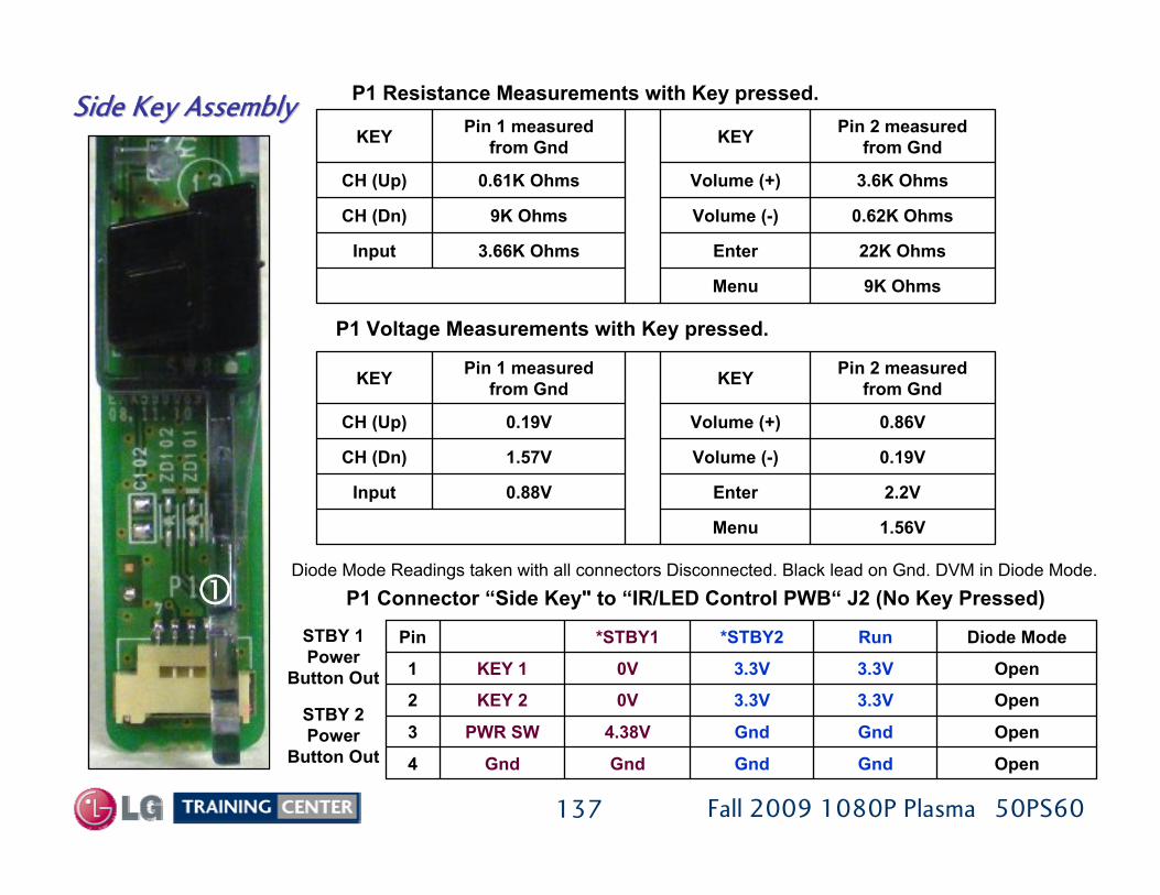
137 Fall 2009 1080P Plasma 50PS60
Side Key AssemblySide Key Assembly P1 Resistance Measurements with Key pressed.
Menu
Enter
Volume (-)
Volume (+)
KEY
9K Ohms
22K Ohms
0.62K Ohms
3.6K Ohms
Pin 2 measured from Gnd
3.66K Ohms
9K Ohms
0.61K Ohms
Pin 1 measured from Gnd
Input
CH (Dn)
CH (Up)
KEY
P1 Voltage Measurements with Key pressed.
P1 Connector “Side Key" to “IR/LED Control PWB“ J2 (No Key Pressed)
Gnd
PWR SW
KEY 2
KEY 1
Gnd
Gnd
3.3V
3.3V
*STBY2
OpenGndGnd4
OpenGnd4.38V3
Open3.3V0V2
Open3.3V0V1
Diode ModeRun *STBY1PinSTBY 1Power
Button Out
Diode Mode Readings taken with all connectors Disconnected. Black lead on Gnd. DVM in Diode Mode.
Menu
Enter
Volume (-)
Volume (+)
KEY
1.56V
2.2V
0.19V
0.86V
Pin 2 measured from Gnd
0.88V
1.57V
0.19V
Pin 1 measured from Gnd
Input
CH (Dn)
CH (Up)
KEY
STBY 2Power
Button Out

138 Fall 2009 1080P Plasma 50PS60
11X17 FOLDOUT 11X17 FOLDOUT ““INTERCONNECT DIAGRAMINTERCONNECT DIAGRAM”” SECTIONSECTION
The following section is the 11 X 17 Foldout The following section is the 11 X 17 Foldout ““InterconnectInterconnect”” drawing. drawing. This drawing is a quick reference, single sheet drawing with This drawing is a quick reference, single sheet drawing with references to many of the repair tips, voltages and layouts givireferences to many of the repair tips, voltages and layouts giving ng during the presentation. during the presentation.
The 11 X 17 foldout is best viewed in the Adobe version in whichThe 11 X 17 foldout is best viewed in the Adobe version in which the the page can be zoomed in and out for easier reading.page can be zoomed in and out for easier reading.

X250Mhz
50PS60 TV INTERCONNECT DIAGRAM
Switch Mode Power Supply
P812
F101-2
SC101
15A / 250V
P813
P811
P811 / P812 “SMPS”
P114Floating
Gnd
P814
Control PWB
P101
P1
Pin Label STBY Run Diode Check1,2 VS 0V 195V
GndNC3
4,56,78
9,10 0V
Open
0.86V
NC
VA
M5V
NCGnd0V
GndOpen
5.0V
NCGnd65V
IC1
P5
P104
P2P200
P101
P102
IC306 P202
P3AUTO GEN
P301P103
P106
P104
P102
P105
P214
P116
P216Floating
GND
P312Floating GND
P314Floating
GND
P311
P313
P101
P307
P111
P211
P112 P309
P101
P102
P103
P104
P201
P202
P203
P204
Odd Waveform
Even Waveform
VSC TP (-)
(-) (+)
R306
R305Even Waveform
Odd Waveform
VSCAN
SET-Dn1
DD_Var (-VY)
SET-Up1
IC7IC12
IC304 IC16
FS901 5V4A 125V
FS303 VA10A 125V
FS302 VS3A 250V
N/C
n/c
N/C
N/C
P100
(+)VZB TP
R457VZB
(-)VZB TP
FS100 5V4A 125V
VR601
VR902
VR602
VR901
VR201
Pin Label STBY Run Diode Check1,2,3,4 0V 5V5,6,7,8
0.75V5V
P813 “SMPS” - P200 “CONTROL”
IC71 (0V)2 (3.3V)3 (5.0V)
IC121 (0V)2 (2.5V)3 (5.0V)
IC3041 (0V)2 (3.3V)3 (5.0V)
SMPS TEST: Removing connector P814 will force the SMPS into full run mode. Only do this with AC power removed then reapply AC power.
Q93
Q94
Q95
Q96
Q97
Q98
Q99
Q73
Q81
Q82
Q83
Q72
Q71
D72
D74
D52
Q51
Q52
Q61
D51
Q62
D61
D62
Q11
Q12
D16
D17
D31
Q30
Q31
Q40
D30
Q41
D40
D41
Q10
Q22
Q21
Q20
D7
D6
P6
VA Adj
VS Adj
Fl103Z-SUS TP
FS102 VS3A 250V
P121
IC1671 (0V)2 (3.3V)3 (5.0V)
Q15
Q14
Q13
AUTO GEN is activated by shorting pin 1 to pin 2 of connector P6. Note: The LVDS cable must be removed for Auto Gen to work.
P814 “SMPS” - P1108 “MAIN”
*If pin 24 is at 4.3V with the unit is in standby the Power Button is released and will prevent the unit from coming on.
P100 “Z-SUS” - P2 “Control”
Z-SUS LOCATION Generic PartD16, 17
D30, 31, 40, 41
RF200145F122Q10, 11, 12, 20, 21, 22, 30, 31, 40, 41
MA3DF30Q13, 14 20NF20Q15 51N25
Pin 1-4 is 3.3V to TCP from IC304 50Mhz TP
*FL55V
Complete testing of the SMPS requires that you load VS with 2 100 watt light bulbs with P811 and P812 unplugged to verify it is functioning correctly.
TIP: If A/C DET is low or missing, Remove AC Det (pin 28) out of P814 and jump it to any pin carrying 5V STBY. Then reapply power to the unit. If the TV now stays on, suspect a defective SMPS.
The 17.8V on pins 1 ~ 4 is derived by the Y-SUS PWB.
Voltages are reference to floating ground.
T901T902
VR901
VR501
D902
D903
D911
(VSC)
Pins 1 ~ 6 are 17.8V
from Y-Sus
P1
IC904
Q901
IC909
IC908ZD902Q903
* FL4 / FL5:These EMI filters have 4 solder tack points the center two are tied to ground.
F8014A 250V
F3021A 250V
Pins 1 ~ 4 are labed as 15V but measures 17.8V.
P100
IC902IC903
S G
D
S G
DA
A
C
C
A
A
C
C
C
D904D914
ZD14.7V
J1
Front PWB IR Receiver
Power Button
J2
Side (Key) Controls P1
These voltages are reference to floating GND. LOC DevelopesD902 +VyD903D911
D912
Vsc
D914ZD902
LOC Pin 1 Pin 2 IC902 9V 8VIC903
17.9VIC904IC905IC908 23.3VIC909
2.1V
10.5V
1V0V
0V0V
Pin 3Cold Gnd
7.7V5V
15.2V5.0V
1.8V cg.08V cg
N/AN/AN/AN/A
Pin 4
0V
Y-SUS LOCATION Generic Part
D51, 52, 61, 62, 71, 72
Q98, 99
Q93, 94, 95, 96, 97 IRFI14229
MA3DF30
45F122
K3667
Q51, 52, 61, 62, 71, 72, 73, 81, 82, 83
34 ~ 5
6 ~ 12
Pin Run V Diode Chk1 ~ 2 140V
Open
Openncnc
F GndFG5VF Gnd
P116 P214Pin
1 ~ 78 ~ 910
11 ~ 12
Run V
140Vnc
FG5VF Gnd
Diode Chk
nc
F GndOpen
Open
Diode test is reference to floating GND (F Gnd)
NOTE: Diode tests are conducted with the PWB disconnected.
P307 Y-SUS
*Generic parts list for sub supplies located in and above Y-SUS.
10
Pin Label Run Diode Check1~4 15V 17.8V
5
ER-DN2.2V6
78 Gnd9
GndSUS-UP11
1.49VGnd
Gnd
Gnd.5V
ER-UP
Z Bias
Gnd Gnd
1.8V
1.2V
0V0V
Gnd3.0VGnd0.4V
SUS-DN12 .5V0.7V
13,14,15
Open
Pin Label STBY Run Diode Check1,2 17V 0V 17V3,4
Open5,67,8
9,10, 12 5V 11
NC1617 0V
2.2V
1.2V
NC1.45V
12V
5V STBY
5V DET
0V
0.5V5V Open
18 5V 1.45VA/C DET
NC4.7V
12V
5V5V
5V
NC
RL ON19VS ON20
21 0VOpenOpenM5V ON
0V Open
22 0V OpenAUTO GND
0V3.3V
3.3V
0V
3.2V
23 5V OpenSTBY 5*24 *0VKEY ON
5.0V*0V
8 ~ 910
11~12
Pin Run V Diode Chk1 ~ 7
P313P311Pin Run V
140Vnc5V
F GndDiode Chk
nc
F Gnd1.3V
2.7V
NCNC NC NC
Gnd Gnd GndGnd
Gnd Gnd GndGnd
Gnd Gnd GndGnd
Gnd Gnd GndGnd
P302
34 ~ 5
6 ~ 12
1 ~ 2 140Vnc
FG5VF Gnd
2.7Vnc
1.3VF Gnd
Diode CheckPin Run 1,2,3,4 VA Voltage
5Open
ncnc6,7 GndGnd
Pin Run Diode Check1,2,3,4 VA Voltage
5Open
ncnc6,7 GndGnd
Diode Check
1.48V1.48V
1.48V
1.48V1.48V
Gnd
Pin123456
1.48V
1.4V
1.32V
78
9~12
Note: P2 pins reversed from P100
LOC Source GateQ901 140V 144VQ903 85V
Drain163V275V88V
TIP: To Test Z-SUSWithout a good Y-SUS.1) Light bulb load Vs.2) Jump the 17V from pin 1 or pin 2 P814 to the Z-SUS connector P100 1~5.
Note: The 17V supply will pulsate 2 to 3 times a second with Vs unloaded.
1~ 2 pins Y-Drive
Logic Sig
P1103.3V inon Pins57~60
P2103.3V in onPins 57~60
P3103.3V in onPins 57~60
P320Va in on
Pins 19~30
P221Va out onPins 1~12P220
Va in onPins 19~30
P120Va outon Pins 1~12
P101 P102 P103 P104 P105 P106 P107 P108 P301 P302 P303 P304 P305 P306 P307 P308P201 P202 P203 P204 P205 P206 P207
P1RunStbyPin3.3V1~2
3
Gnd4
Gnd
If Power Button is open,
pin 3 (4.38V)
3.3V
Gnd
Gnd
Y-SUS
Z-SUS
X-Board RightX-Board Center
Pin 1-4 is 3.3V to TCP from IC304
Pin 1-4 is 3.3V to TCP from IC304
Pins 1~4 (5V)Pins 9~12 17.8V
D909D910
D902 = (+Vy) FGD903 = (Vsc) FGD909 / D910 = 17.8VD911 = (15V FG)D912 = (5V FG)
Cathode180V
10.58V
23.3V163V
5.0V15.3V
15VFG
5VFG5VFG Reg
D913 23.3V15VFG Reg
IC905
Cold Gnd
Feedback
3VAnodeZD902
D904 163V 180VA C
Across +Vy VscFloating Gnd
*FL45V
+Vy
Vsc
15VFG
D9125VFG
cgfg cgfg
Fg = Floating Gnd cg = Chassis Gnd
17.8VSource
P310
Anode:D909,D910
30V p/p
4~5 pins FG5V6~12 pins FG
11~12 Y-Drive
8~9 FG5V1~7 FG
ZD2 ZD3Cold Gnd
Black wire is not Pin 1
P2 “Control”
LVDS
1.5V0V0V151.7V0V0VLED
W141.87V0V3.19VLED R13GndGndGndGnd120.6V5V0.56V+5V111.25V5V5VSTBY
5V10GndGndGndGnd92V3.3V3VEYEQ-SDA82V3.3V3VEYEQ-SCL7
GndGndGndGnd6
Gnd / Open0V0V/
4.3VKey On*51.9V3.29V3.29VKey241.9V3.29V3.29VKey13GndGndGndGnd22V3.98V4VIR1
Run STBYLabelPin
1.5V0V0VLED Cent151.7V0V0VLED W141.87V0V3.19VLED R13GndGndGndGnd120.6V5V0.56V+5V111.25V5V5VSTBY 5V10GndGndGndGnd92V3.3V3V82V3.3V3VEYEQ SCL7
GndGndGndGnd6Gnd / Open0V0V/4.3VKey On*5
1.9V3.29V3.29VKey241.9V3.29V3.29VKey13GndGndGndGnd22V3.98V4VIR1
Diode CheckRun STBYLabelPin
EYEQ SDA
P1101 “Main” - J1 “Ft IR”
Pin 5: When the Power Button is opened, Pin 5: pulls up to 4.3V.Pin 10: Stand-By 5V turns off.
D7 showsPWB
running OK
D6 blink pattern shows temperature
FS301M5V
4A/125VFS301
1
TUNER
SIF 16
19 Video
(5V) 4
DIF + 12DIF - 13
(5V) 15
D502
IC952IC302
IC503
X1
X501IC201
P1006 P1003 LVDSP1001
P1005Speakers
IC1
IC801
IC504HDMI
USB
IC805
A=5VA=0V
K=4.7V
D303
Q1002
Q303
IC203
D805
D804
Q801
K AZD601
D951IC202
31 2
IC304
IC201
21 3
2
D801
B
C
EB
C
E
B
C
E
Q951
Q891
Q503
2
C A
D1001
Q302
Q1001
IC601
A
K
AD802IC803
IC802
Q892
A
K
A
D628
Q601
D627A
K
AB
C
EQ890
Q305
B
C
E
B
C
E
IC602
A
K
A
Q502
B
C
E
IC204
IC301
Q301
G
D
S
B
C
E
1
3
2
B
C
E
B CE
A
C
AA
C
A
D633
Main Run / *Stby Voltages
*If no voltage is shown for Stby then it is 0V.
EB 3.3V 3.19VC
0.6VEB 0VC
Q601
0V
5.0VQ8011-0V
2-3.1V3-3.2V
S 4.9V
G 4.9VD 0V
Q890/20V0V0V
0V/0.6V3.28V/0V
Q8910V0V0V
2.16V0V
Q9510V0V0V
0V
Q301 Q302 Q303 Q501 Q5021.6VGnd3.29V0V
Q5032.37V
3.0V0V
Q10010V0V
3.28V
Q10020V
0.6V0V
Y-SUS LOCATION
Q901:FQB27N25
KTN2222AUQ902, Q904:
IC902, IC903:LTV817MVBIC904:KIA431AF
Q903:FQB6N70
BA17BM15TIC908, IC909:
IC905:KIA78M05F
4-3.2V
3
21
4
7
Pin1 5.4V Gnd
2
0V345 0.9V6
4.85V3.57V8
1.3V
1.1V
4.89VGndGnd
4.65V4.65V4.65V4.65V
HDMI3
GndGndGndGnd
4.67V0V
4.67V4.67V
0V0V0V0V
3.28V3.28V
0V3.28V
0V0V
3.28V0V
3.28V3.28V3.28V3.28V
Gnd
IC302 IC805 IC952IC201 IC202
EDIDHDCPNVRAM 1.3VVDDC
IC602RS232Flash0V0V0V0V
4.54V4.54V
IC802
GndGndGndGnd4.6V4.6V
3.3V4.5V
3.3V4.6V
GndGndGndGnd4.6V4.6V3.3V4.6V
IC803HDMI1EDID
HDMI2EDID
1) 5.1V2) Gnd
5) 0V6) 5.1V
3) 3.2V4) 0V
IC804 USB
D806AK A
AK A
HDMI4EDID
B
C
E
CA
A-C
8V
5V Reg
AnalogS (0V)G (3.3V)D (3.3V)
S (3.3V)G (0V)D (3.3V)
I/O
Q504Digital
12 3.3V 3.0V3 5V
1.85V3.3V
0.6VIn
Out0V8V0V
Reg 9V Reg
12VGnd4.9V0V
5.0V
3.8V
IC301 IC305 IC304 IC502 IC503 IC5051.8VMST
Reg3.3VMST
Reg3.3VST
On = Digital CH1.2VPVSB Reg
0V/3.3V0V/1.2V
IC502
Q504
Q501C
B E
GndOutIn
Out
D
G S
2
3 2 1
IC505
160us ± 5us-VY
A
B
Set-dn VR601
Set-up VR602
0V
100uS100VScope Settings
Flat Period:
B
VS
VSC
10 ± 5usA 78V RMS
520V p/p
Note: If AC Det (Pin 18) is missing, the set will come on like normal, then in under 10 seconds it will turn off.
41V RMS 260V p/p
Pin 17 (5V Det) not used.
Pins 1,2 (17V) turned on with Vs On.
Pins 9,10,12 (+5V) turned on with Relay On Command.
+VY TP
Read in White Wash
Read in White Wash
P302
0.86V
Open
NC6,78
9,10
Diode CheckPinDiode CheckPin
NC
Open
Gnd
1,2
34,5

50PS60 LVDS P1003 WAVEFORMSWAVEFORMS:Waveforms taken using SMTP Color Bar input. All readings give their Time Base related to scope settings. All waveforms taken from the P1003.
MAIN PWB VIDEO TEST POINT (Pin 28) MAIN PWB VIDEO TEST POINT (Pin 27)
MAIN PWB VIDEO TEST POINT (Pin 17) MAIN PWB VIDEO TEST POINT (Pin 16)
MAIN PWB VIDEO TEST POINT (Pin 22) MAIN PWB VIDEO TEST POINT (Pin 21)
MAIN PWB VIDEO TEST POINT (Pin 12)
1V per/div 2mSec per/div 7.25V p/p
MAIN PWB VIDEO TEST POINT (Pin 11)
1V per/div 2mSec per/div 5.25V p/p1V per/div 2mSec per/div 6.4V p/p1V per/div 2mSec per/div 5.25V p/p
200mV per/div 10uSec per/div 900mV p/p 1V per/div 10uSec per/div 6V p/p 1V per/div 10uSec per/div 6.25V p/p 1V per/div 10uSec per/div 7V p/p
NOTE: LVDS P1003 InformationThere are actually 20 pins carrying Video plus 4 pins carrying clock signals to the Control board. Only 8 are shown as an example of what signals are on each pin.

50PS60 MAIN (BACK SIDE) SIMICONDUCTORS
IC201 NVRAM IC304 1.8VMST IC505 5V (Tuner) IC602 RS232 RAM Q1001 Pow Down Q502 Video Buffer Q890/2 HDMI1/2Pin Pin Reg Pin Reg Pin Pin IC1001 Pin Pin Hot Swap[1] Gnd [1] 0.6V [1] 3.8V [1] Gnd [B] 0V [B] 0.6V [B] 0V[2] Gnd [2] 1.8V [2] 5V [2] Gnd [E] Gnd [E] 2.1V [E] Gnd[3] Gnd [3] 3.28V [3] 8V [3] Gnd [C] 3.3V [C] Gnd [C] 0V[4] Gnd [4] Gnd[5] 3.28V [5] 4.5V Q302 Reset Q503 SIF Buffer Q891/951 HDMI3/4[6] 3.28V IC601 RS232 Control [6] 4.5V Pin Pin Pin Hot Swap[7] 0V IC305 3.3VMST Pin [7] 3.3V [B] 3.3V [B] 2.3V [B] 0V[8] 3.28V Pin Reg [1] 3.3V [8] 4.5V [E] 3.2V [E] 3.0V [E] Gnd
[1] Gnd [2] 5.4V [C] 0V [C] Gnd [C] 0VIC202 HDCP [2] 3.0V [3] 0V IC802/3 HDMI1/2
Pin [3] 4.9V [4] 0V Pin Q303 Reset Q501 1.2V PVSB[1] Gnd [5] 5.3V [1] Gnd Pin Pin Switch[2] Gnd [6] 5.3V [2] Gnd [S] 4.9V [S] 3.3V[3] 3.28V [7] 5.3V [3] Gnd [G] 4.9V [G] 3.3V/0V[4] Gnd IC502 1.2V PVSB [8] 0V [4] Gnd [D] 0V [D] 0V/3.27V[5] 3.28V On Digital CH / Off Analog [9] 3.3V [5] 4.5V On Digital CH / Off Analog[6] 3.28V Pin Reg [10] 3.3V [6] 4.5V Q501 1.2V PVSB[7] 3.28V Gnd Gnd [11] 0.3V [7] 3.3V Pin Switch Q601 RS232 TX[8] 3.28V In 0V/3.3V [12] 3.3V [8] 4.5V [B] 0V/0.6V Pin Buffer
Out 0V/1.2V [13] 0V [E] 0V [B] 0.6VIC301 3.3V VST [14] 5.4V [C] 3.3V/0V [E] Gnd
Pin [15] 0V On Digital CH / Off Analog [C] 0V[1] Gnd [16] 3.3V[2] 3.3V D1001 IC1001 D951 HDMI4 PWR D627 RS232 TX Noise D628 RS232 RX Noise D633 RGB B+ D801 EDID B+ D802 HDMI CEC[3] 5.0V Pin Reset Limit Pin Pin Suppression Pin Suppression Pin Pin Pin B+
A 3.27V A 5.1V A (-5.3V) A 0V A 0V A 4.6V A 0VC 3.3V C 4.65V C 0.1V C 0V C 4.5V C 4.9V C 3.17V
A 0V A Gnd A Gnd A 5.0V A 5.1V A 3.27V
50PS60 MAIN (FRONT SIDE) SIMICONDUCTORSIC302 1.3V VDDC IC804 USB 5V IC952 HDMI4 EDID Q301 Turns on
Pin Pin Pin Pin Q303[1] 5.47V [1] 5.0V [1] Gnd [B] 0.54V[2] 4.89V [2] Gnd [2] Gnd [E] Gnd[3] 1.3V [3] 3.2V [3] Gnd [C] 0V[4] Gnd [4] 0V [4] Gnd[5] 0.9V [5] 0V [5] 4.65V Q801 HDMI CEC[6] 1.19V [6] 5.1V [6] 0V Pin Amp[7] 4.85V [7] 4.65V [1] 0V[8] 3.55V [8] 4.65V [2] 3.16V
[3] 3.27VIC503 9V Reg IC805 HDMI3 EDID [4] 3.28V
Pin Pin D303 Reset[1] 10V [1] Gnd Pin Q1002 Pow Down[2] Gnd [2] Gnd A 3.18V Pin IC1001[3] 8V [3] Gnd AC 3.28V [B] 0.6V
[4] Gnd C 3.28V [E] Gnd[5] 4.65V [C] 0V[6] 4.65V[7] 3.31V[8] 4.65V
D804 HDMI1 PWR D805 HDMI2 PWR D806 HDMI3 PWRPin Pin Pin
A 5.1V A 5.1V A 5.1VC 4.65V C 4.65V C 4.65VA 0V A 0V A 0V