5 V powered multi-channel RS-232 drivers and receivers · 1.3 3.5 µs Notes: (1)Measured from 3 V...
18
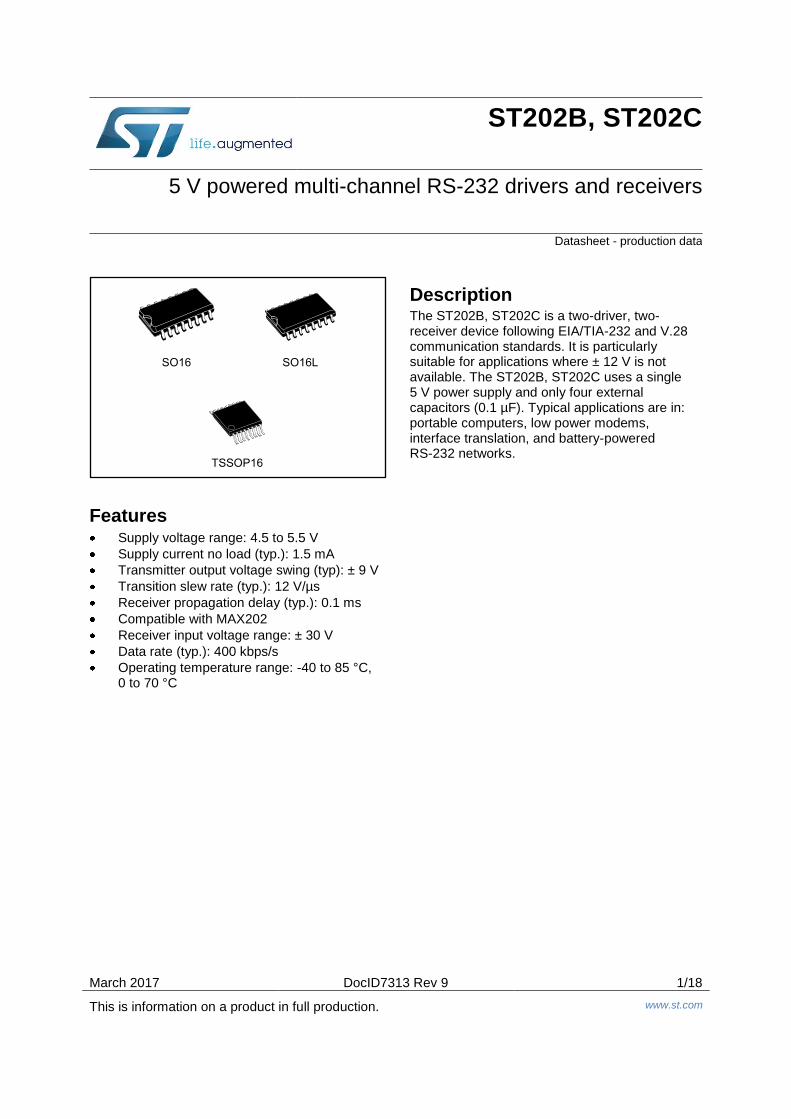
March 2017 DocID7313 Rev 9 1/18 This is information on a product in full production. www.st.com ST202B, ST202C 5 V powered multi-channel RS-232 drivers and receivers Datasheet - production data Features Supply voltage range: 4.5 to 5.5 V Supply current no load (typ.): 1.5 mA Transmitter output voltage swing (typ): ± 9 V Transition slew rate (typ.): 12 V/μs Receiver propagation delay (typ.): 0.1 ms Compatible with MAX202 Receiver input voltage range: ± 30 V Data rate (typ.): 400 kbps/s Operating temperature range: -40 to 85 °C, 0 to 70 °C Description The ST202B, ST202C is a two-driver, two- receiver device following EIA/TIA-232 and V.28 communication standards. It is particularly suitable for applications where ± 12 V is not available. The ST202B, ST202C uses a single 5 V power supply and only four external capacitors (0.1 μF). Typical applications are in: portable computers, low power modems, interface translation, and battery-powered RS-232 networks.
-
Upload
nguyenthuan -
Category
Documents
-
view
213 -
download
0
Transcript of 5 V powered multi-channel RS-232 drivers and receivers · 1.3 3.5 µs Notes: (1)Measured from 3 V...
March 2017 DocID7313 Rev 9 1/18
This is information on a product in full production. www.st.com
ST202B, ST202C
5 V powered multi-channel RS-232 drivers and receivers
Datasheet - production data
Features Supply voltage range: 4.5 to 5.5 V
Supply current no load (typ.): 1.5 mA
Transmitter output voltage swing (typ): ± 9 V
Transition slew rate (typ.): 12 V/µs
Receiver propagation delay (typ.): 0.1 ms
Compatible with MAX202
Receiver input voltage range: ± 30 V
Data rate (typ.): 400 kbps/s
Operating temperature range: -40 to 85 °C, 0 to 70 °C
Description The ST202B, ST202C is a two-driver, two-receiver device following EIA/TIA-232 and V.28 communication standards. It is particularly suitable for applications where ± 12 V is not available. The ST202B, ST202C uses a single 5 V power supply and only four external capacitors (0.1 µF). Typical applications are in: portable computers, low power modems, interface translation, and battery-powered RS-232 networks.

Contents ST202B, ST202C
2/18 DocID7313 Rev 9
Contents
1 Pinout information ........................................................................... 3
2 Absolute maximum ratings ............................................................. 4
3 Electrical characteristics ................................................................ 5
4 Typical application .......................................................................... 7
5 Typical performance characteristics ............................................. 8
6 Package information ....................................................................... 9
6.1 SO16 package information .............................................................. 10
6.2 SO16L package information ............................................................ 11
6.3 TSSOP16 package information ....................................................... 12
6.4 SO16 tape and reel package information ........................................ 13
6.5 SO16L tape and reel package information ...................................... 14
6.6 TSSOP16 tape and reel package information ................................. 15
7 Ordering information ..................................................................... 16
8 Revision history ............................................................................ 17

ST202B, ST202C Pinout information
DocID7313 Rev 9 3/18
1 Pinout information Figure 1: Pin connections (top view)
Table 1: Pin description
Pin n° Symbol Name and function
1 C1+ Positive terminal for the first charge pump capacitor
2 V+ Doubled voltage terminal
3 C1- Negative terminal for the first charge pump capacitor
4 C2+ Positive terminal for the second charge pump capacitor
5 C2- Negative terminal for the second charge pump capacitor
6 V- Inverted voltage terminal
7 T2OUT Second transmitter output voltage
8 R2IN Second receiver input voltage
9 R2OUT Second receiver output voltage
10 T2IN Second transmitter input voltage
11 T1IN First transmitter input voltage
12 R1OUT First receiver output voltage
13 R1IN First receiver input voltage
14 T1OUT First transmitter output voltage
15 GND Ground
16 VCC Supply voltage

Absolute maximum ratings ST202B, ST202C
4/18 DocID7313 Rev 9
2 Absolute maximum ratings
Absolute maximum ratings are those values beyond which damage to the device may occur. Functional operation under these conditions is not implied.
Table 2: Absolute maximum ratings
Symbol Parameter Value Unit
VCC Supply voltage –0.3 to 6
V
V+ Extra positive voltage (VCC – 0.3) to 13.2
V- Extra negative voltage 0.3 to -13.2
TIN Transmitter input voltage range -0.3 to (VCC + 0.3)
RIN Receiver input voltage range ± 30
TOUT Transmitter output voltage range ± 15
ROUT Receiver output voltage range –0.3 to (VCC + 0.3)
TSCTOUT Short circuit duration on TOUT Infinite

ST202B, ST202C Electrical characteristics
DocID7313 Rev 9 5/18
3 Electrical characteristics Table 3: Electrical characteristics, C1 - C4 = 0.1 µF, VCC = 5 V ± 10 %, TA = –40 to 85 °C, unless
otherwise specified, typical values are referred to TA = 25 °C
Symbol Parameter Test conditions Min. Typ. Max. Unit
ISUPPLY VCC power supply current No load — 1.5 4 mA
Table 4: Transmitter electrical characteristics, C1 - C4 = 0.1 µF, VCC = 5 V ± 10 %, TA = –40 to 85 °C, unless otherwise specified, typical values are referred to TA = 25 °C
Symbol Parameter Test conditions Min. Typ. Max. Unit
VTOUT Output voltage swing All transmitter outputs are loaded with 3 kΩ to GND
± 5 ± 9
V
ITIL Logic pull-up current TIN = 0 V
5 40 µA
VTIL Input logic threshold
low 0.8 1.4
V
VTIH Input logic threshold
high 1.4 2
SRT Transition slew rate TA = 25 °C, VCC = 5 V, RL = 3 to
7 kΩ, CL = 50 to 2500 pF (1) 6 12 30 V/µs
DR Data rate (2) 200 400
kbits/s
RTOUT Transmitter output
resistance VCC = V+ = V- = 0 V,
VOUT = ± 2 V 300
Ω
ISC Transmitter output short circuit current
One TXOUT to GND ± 7 ± 22
mA
tDT Propagation delay time TTL-CMOS IN to RS-232 OUT,
CL = 150 pF (50 % to 50 %) 1.3 3.5 µs
Notes:
(1)Measured from 3 V to -3 V or from -3 V to 3 V (2)One transmitter output is loaded with RL = 3 kΩ to 7 kΩ, CL = 50 to 1000 pF

Electrical characteristics ST202B, ST202C
6/18 DocID7313 Rev 9
Table 5: Receiver electrical characteristics, C1 - C4 = 0.1 µF, VCC = 5 V ± 10 %, TA = –40 to 85 °C, unless otherwise specified, typical values are referred to TA = 25 °C
Symbol Parameter Test
conditions Min. Typ. Max. Unit
VRIN Receiver input voltage
operating range -30
30 V
RRIN RS-232 input resistance TA = 25 °C 3 5 7 kΩ
VRIL RS-232 input threshold low
0.8 1.3
V
VRIH RS-232 input threshold high
1.8 2.4
VRIHYS RS-232 input hysteresis VCC = 5 V 0.2 0.5 1
VROL TTL/CMOS output voltage low IOUT = 3.2 mA
(to VCC) 0.2 0.4
VROH TTL/CMOS output voltage high IOUT = 1 mA
(to GND) 3.5 VCC - 0.2
ISCR Receiver output short circuit current To GND 2 10
mA To VCC 10 30
tDR Propagation delay time CL = 150 pF (1)
0.1 0.5 µs
Notes:
(1)RS-232 in to TTL-CMOS out (from 50 % to 50 %)

ST202B, ST202C Typical application
DocID7313 Rev 9 7/18
4 Typical application Figure 2: Application circuit
1. C1-4 can be replaced by the 1 µF capacitors 2. C1-4 can be common or biased capacitors
Table 6: Capacitance value (µF)
C1 C2 C3 C4 C5
0.1

Typical performance characteristics ST202B, ST202C
8/18 DocID7313 Rev 9
5 Typical performance characteristics
Unless otherwise specified TJ = 25 °C.
Figure 3: Driver voltage transfer characteristics
Figure 4: Drive short circuit output current vs temperature
Figure 5: Receiver threshold vs supply voltage
Figure 6: Driver output capability current vs output voltage
Figure 7: Driver short circuit supply current vs. temperature
Figure 8: Receiver threshold vs temperature

ST202B, ST202C Package information
DocID7313 Rev 9 9/18
6 Package information
In order to meet environmental requirements, ST offers these devices in different grades of ECOPACK® packages, depending on their level of environmental compliance. ECOPACK® specifications, grade definitions and product status are available at: www.st.com. ECOPACK® is an ST trademark.

Package information ST202B, ST202C
10/18 DocID7313 Rev 9
6.1 SO16 package information
Figure 9: SO16 package outline
Table 7: SO16 mechanical data
Ref
Dimensions
Millimeters Inches
Min. Typ. Max Min. Typ. Max.
A
1.75
0.068
a1 0.1
0.25 0.004
0.010
a2
1.64
0.063
b 0.35
0.46 0.013
0.018
b1 0.19
0.25 0.007
0.010
C
0.5
0.019
c1
45 °
45 °
D 9.8
10 0.385
0.393
E 5.8
6.2 0.228
0.244
e
1.27
0.050
e3
8.89
0.350
F 3.8
4.0 0.149
0.157
G 4.6
5.3 0.181
0.208
L 0.5
1.27 0.019
0.050
M
0.62
0.024
S
8 °
8 °

ST202B, ST202C Package information
DocID7313 Rev 9 11/18
6.2 SO16L package information
Figure 10: SO16L package outline
Table 8: SO16L mechanical data
Ref
Dimensions
Millimeters Inches
Min. Typ. Max Min. Typ. Max.
A 2.35
2.65 0.093
0.104
A1 0.1
0.3 0.004
0.012
B 0.33
0.51 0.013
0.02
C 0.23
0.32 0.009
0.013
D 10.1
10.5 0.398
0.413
E 7.4
7.6 0.291
0.299
e
1.27
0.05
H 10
10.65 0.394
0.419
h 0.25
0.75 0.01
0.03
L 0.4
1.27 0.016
0.05
k 0 °
8 ° 0 °
8 °
ddd
0.1
0.004

Package information ST202B, ST202C
12/18 DocID7313 Rev 9
6.3 TSSOP16 package information
Figure 11: TSSOP16 package outline
Table 9: TSSOP16 mechanical data
Ref
Dimensions
Millimeters Inches
Min Typ Max Min Typ Max
A
1.20
0.047
A1 0.05
0.15 0.002
0.006
A2 0.80 1.00 1.05 0.031 0.039 0.041
b 0.19
0.30 0.007
0.012
c 0.09
0.20 0.004
0.008
D 4.90 5.00 5.10 0.193 0.197 0.201
E 6.20 6.40 6.60 0.244 0.252 0.260
E1 4.30 4.40 4.50 0.169 0.173 0.177
e
0.65
0.026
k 0°
8° 0°
8°
L 0.45 0.60 0.75 0.018 0.024 0.030
L1
1.00
0.039
aaa
0.10
0.004

ST202B, ST202C Package information
DocID7313 Rev 9 13/18
6.4 SO16 tape and reel package information
Figure 12: SO16 tape and reel package outline
1. Drawing not to scale
Table 10: SO16 tape and reel mechanical data
Ref
Dimensions
Millimeters Inches
Min. Typ. Max Min. Typ. Max.
A
—
330
—
12.992
C 12.8 13.2 0.504 0.519
D 20.2
0.795
N 60
2.362
T
22.4
0.882
Ao 6.45 6.65 0.254 0.262
Bo 10.3 10.5 0.406 0.414
Ko 2.1 2.3 0.082 0.090
Po 3.9 4.1 0.153 0.161
P 7.9 8.1 0.311 0.319

Package information ST202B, ST202C
14/18 DocID7313 Rev 9
6.5 SO16L tape and reel package information
Figure 13: SO16L tape and reel package outline
1. Drawing not to scale
Table 11: SO16L tape and reel mechanical data
Ref
Dimensions
Millimeters Inches
Min. Typ. Max Min. Typ. Max.
A
—
330
—
12.992
C 12.8 13.2 0.504 0.519
D 20.2
0.795
N 60
2.362
T
22.4
0.882
Ao 10.8 11.0 0.425 0.433
Bo 10.7 10.9 0.421 0.429
Ko 2.9 3.1 0.114 0.122
Po 3.9 4.1 0.153 0.161
P 11.9 12.1 0.468 0.476

ST202B, ST202C Package information
DocID7313 Rev 9 15/18
6.6 TSSOP16 tape and reel package information
Figure 14: TSSOP16 tape and reel package outline
1. Drawing not to scale
Table 12: TSSOP16 tape and reel mechanical data
Ref
Dimensions
Millimeters Inches
Min. Typ. Max Min. Typ. Max.
A
—
330
—
12.992
C 12.8 13.2 0.504 0.519
D 20.2
0.795
N 60
2.362
T
22.4
0.882
Ao 6.7 6.9 0.264 0.272
Bo 5.3 5.5 0.209 0.217
Ko 1.6 1.8 0.063 0.071
Po 3.9 4.1 0.153 0.161
P 7.9 8.1 0.311 0.319

Ordering information ST202B, ST202C
16/18 DocID7313 Rev 9
7 Ordering information Table 13: Order codes
Order code Temperature range Package Packaging Marking
ST202BDR -40 to 85 °C S016 (tape and reel)
2500 parts per reel
ST202B
ST202CDR 0 to 70 °C ST202C
ST202BTR -40 to 85 °C TSSOP16 (tape and reel) ST202B
ST202CWR 0 to 70 °C S016L (tape and reel) 1000 parts per reel ST202C

ST202B, ST202C Revision history
DocID7313 Rev 9 17/18
8 Revision history Table 14: Document revision history
Date Revision Changes
09-Mar-2006 5 Order codes updated and the document has been reformatted.
16-Jul-2007 6 Device summary updated.
14-Nov-2007 7 Modified: Table 1.
11-Feb-2008 8 Modified: Table 1 on page 1.
03-Mar-2017 9
Cover image: replaced silhouettes "SOP" and "SOP Large" with SO16
and SO16L respectively.
Features: updated units of transition slew rate (typ.) from 12 V/ms to
12 V/µs.
Moved “Device summary” table to Section 7: "Ordering information"
section. Removed obsolete order codes ST202BD and ST202CTR
from this table and added "Markings".
Section 6.2: "SO16L package information": replaced package outline
and mechanical data.
Section 6.3: "TSSOP16 package information": added dimensions “L1”
and “aaa”, replaced dimension “K” with “k”, and removed BSC from
dimension “e”.

ST202B, ST202C
18/18 DocID7313 Rev 9
IMPORTANT NOTICE – PLEASE READ CAREFULLY
STMicroelectronics NV and its subsidiaries (“ST”) reserve the right to make changes, corrections, enhancements, modifications, and improvements to ST products and/or to this document at any time without notice. Purchasers should obtain the latest relevant information on ST products before placing orders. ST products are sold pursuant to ST’s terms and conditions of sale in place at the time of order acknowledgement.
Purchasers are solely responsible for the choice, selection, and use of ST products and ST assumes no liability for application assistance or the design of Purchasers’ products.
No license, express or implied, to any intellectual property right is granted by ST herein.
Resale of ST products with provisions different from the information set forth herein shall void any warranty granted by ST for such product.
ST and the ST logo are trademarks of ST. All other product or service names are the property of their respective owners.
Information in this document supersedes and replaces information previously supplied in any prior versions of this document.
© 2017 STMicroelectronics – All rights reserved