4th Generation USB 2.0 Flash Media Controller with ... · - Older CF card support - Force USB 1.1...
30
2004 - 2016 Microchip Technology Inc. DS00002119A-page 1 Hub Controller • Provides Three USB 2.0 Downstream Ports via internal USB 2.0 Hub - Multi Transaction Translator for FS/LS devices attached Flash Media Controller • Complete System Solution for interfacing Smart- Media TM (SM) or xD Picture Card TM (xD) 1 , Mem- ory Stick TM (MS), High Speed Memory Stick (HSMS), Memory Stick PRO (MSPRO), MS Duo TM , Secure Digital (SD), Mini-Secure Digital (Mini-SD), TransFlash (SD), MultiMediaCard TM (MMC), Reduced Size MultiMediaCard (RS- MMC), NAND Flash, Compact Flash TM (CF) and CF Ultra TM I & II, and CF form-factor ATA hard drives to USB 2.0 bus - Supports USB Bulk Only Mass Storage Com- pliant Bootable BIOS • Support for simultaneous operation of all above devices. (only one at a time of each of the follow- ing groups supported: CF or ATA drive, SM or XD or NAND, SD or MMC) • On-Chip 4-Bit High Speed Memory Stick and MS PRO Hardware Circuitry • On-Chip firmware reads and writes High Speed Memory Stick and MS PRO • 1-bit ECC correction performed in hardware for maximum efficiency • Hardware support for SD Security Command Extensions • 3.3 Volt I/O with 5V input tolerance on VBUS, Port Power and Over-Current Sense pins • On-chip power FETs for supplying flash media card power with minimum board components • 8051 8 bit microprocessor - Provides low speed control functions - 30 MHz execution speed at 4 cycles per instruction average - 12K Bytes of internal SRAM for general pur- pose scratchpad - 768 Bytes of internal SRAM for general pur- pose scratchpad or program execution while re-flashing external ROM - Double Buffered Bulk Endpoint - Bi-directional 512 Byte Buffer for Bulk End- point - 64 Byte RX Control Endpoint Buffer - 64 Byte TX Control Endpoint Buffer • Internal Program Memory Interface - 64K Byte Internal Code Space • On Board 24MHz Crystal Driver Circuit • Can be clocked by an external 24MHz source • On-Chip 1.8V Regulator for Low Power Core Operation • Internal PLL for 480MHz USB 2.0 Sampling, Con- figurable MCU clock • 11 GPIOs for special function use: LED indicators, button inputs, power control to memory devices, etc. - Inputs capable of generating interrupts with either edge sensitivity • Configuration of Hub and Flash Media features controlled either by internal defaults or via single external EEPROM. User configurable features: - Full or Partial Card compliance checking - LUN configuration and assignment - Write Protect Polarity - Cover Switch operation for xD compliance - Inquiry Command operation - SD Write Protect operation - Older CF card support - Force USB 1.1 reporting - Internal or External Power FET operation • Compatible with Microsoft WinXP, WinME, Win2K SP3&4, Apple OS10 and Linux Multi-LUN Mass Storage Class Drivers • Win2K, Win98/98SE and Apple OS8.6 and OS9 Multi-LUN Mass Storage Class Drivers are avail- able from Microchip • 128-Pin TQFP Package (1.0mm height, 14mm x14mm footprint); RoHS compliant package also available 1.xD Picture Card not applicable to USB2601 USB2601/USB2602 4th Generation USB 2.0 Flash Media Controller with Integrated Card Power FETs & HS Hub
Transcript of 4th Generation USB 2.0 Flash Media Controller with ... · - Older CF card support - Force USB 1.1...

USB2601/USB2602
4th Generation USB 2.0 Flash Media Controller with Integrated Card Power FETs & HS Hub
Hub Controller
• Provides Three USB 2.0 Downstream Ports via internal USB 2.0 Hub
- Multi Transaction Translator for FS/LS devices attached
Flash Media Controller
• Complete System Solution for interfacing Smart-MediaTM (SM) or xD Picture CardTM (xD)1, Mem-ory StickTM (MS), High Speed Memory Stick (HSMS), Memory Stick PRO (MSPRO), MS DuoTM, Secure Digital (SD), Mini-Secure Digital (Mini-SD), TransFlash (SD), MultiMediaCardTM (MMC), Reduced Size MultiMediaCard (RS-MMC), NAND Flash, Compact FlashTM (CF) and CF UltraTM I & II, and CF form-factor ATA hard drives to USB 2.0 bus
- Supports USB Bulk Only Mass Storage Com-pliant Bootable BIOS
• Support for simultaneous operation of all above devices. (only one at a time of each of the follow-ing groups supported: CF or ATA drive, SM or XD or NAND, SD or MMC)
• On-Chip 4-Bit High Speed Memory Stick and MS PRO Hardware Circuitry
• On-Chip firmware reads and writes High Speed Memory Stick and MS PRO
• 1-bit ECC correction performed in hardware for maximum efficiency
• Hardware support for SD Security Command Extensions
• 3.3 Volt I/O with 5V input tolerance on VBUS, Port Power and Over-Current Sense pins
• On-chip power FETs for supplying flash media card power with minimum board components
• 8051 8 bit microprocessor
- Provides low speed control functions
- 30 MHz execution speed at 4 cycles per instruction average
- 12K Bytes of internal SRAM for general pur-pose scratchpad
- 768 Bytes of internal SRAM for general pur-pose scratchpad or program execution while re-flashing external ROM
- Double Buffered Bulk Endpoint
- Bi-directional 512 Byte Buffer for Bulk End-point
- 64 Byte RX Control Endpoint Buffer
- 64 Byte TX Control Endpoint Buffer
• Internal Program Memory Interface
- 64K Byte Internal Code Space
• On Board 24MHz Crystal Driver Circuit• Can be clocked by an external 24MHz source• On-Chip 1.8V Regulator for Low Power Core
Operation• Internal PLL for 480MHz USB 2.0 Sampling, Con-
figurable MCU clock• 11 GPIOs for special function use: LED indicators,
button inputs, power control to memory devices, etc.
- Inputs capable of generating interrupts with either edge sensitivity
• Configuration of Hub and Flash Media features controlled either by internal defaults or via single external EEPROM. User configurable features:
- Full or Partial Card compliance checking
- LUN configuration and assignment
- Write Protect Polarity
- Cover Switch operation for xD compliance
- Inquiry Command operation
- SD Write Protect operation
- Older CF card support
- Force USB 1.1 reporting
- Internal or External Power FET operation
• Compatible with Microsoft WinXP, WinME, Win2K SP3&4, Apple OS10 and Linux Multi-LUN Mass Storage Class Drivers
• Win2K, Win98/98SE and Apple OS8.6 and OS9 Multi-LUN Mass Storage Class Drivers are avail-able from Microchip
• 128-Pin TQFP Package (1.0mm height, 14mm x14mm footprint); RoHS compliant package also available
1.xD Picture Card not applicable to USB2601
2004 - 2016 Microchip Technology Inc. DS00002119A-page 1

USB2601/USB2602
TO OUR VALUED CUSTOMERS
It is our intention to provide our valued customers with the best documentation possible to ensure successful use of your Microchipproducts. To this end, we will continue to improve our publications to better suit your needs. Our publications will be refined andenhanced as new volumes and updates are introduced.
If you have any questions or comments regarding this publication, please contact the Marketing Communications Department viaE-mail at [email protected]. We welcome your feedback.
Most Current Data SheetTo obtain the most up-to-date version of this data sheet, please register at our Worldwide Web site at:
http://www.microchip.com
You can determine the version of a data sheet by examining its literature number found on the bottom outside corner of any page. The last character of the literature number is the version number, (e.g., DS30000000A is version A of document DS30000000).
ErrataAn errata sheet, describing minor operational differences from the data sheet and recommended workarounds, may exist for cur-rent devices. As device/documentation issues become known to us, we will publish an errata sheet. The errata will specify therevision of silicon and revision of document to which it applies.
To determine if an errata sheet exists for a particular device, please check with one of the following:• Microchip’s Worldwide Web site; http://www.microchip.com• Your local Microchip sales office (see last page)
When contacting a sales office, please specify which device, revision of silicon and data sheet (include -literature number) you areusing.
Customer Notification SystemRegister on our web site at www.microchip.com to receive the most current information on all of our products.
DS00002119A-page 2 2004 - 2016 Microchip Technology Inc.

2004 - 2016 Microchip Technology Inc. DS00002119A-page 3
USB2601/USB2602
Table of Contents
1.0 Introduction ..................................................................................................................................................................................... 42.0 Pin Table ......................................................................................................................................................................................... 63.0 Pin Configuration ............................................................................................................................................................................ 94.0 Block Diagram ............................................................................................................................................................................... 105.0 Pin Descriptions ............................................................................................................................................................................ 116.0 DC Parameters ............................................................................................................................................................................. 177.0 Package Information ..................................................................................................................................................................... 238.0 GPIO Usage .................................................................................................................................................................................. 25Appendix A: Data Sheet Revision History ........................................................................................................................................... 26The Microchip Web Site ...................................................................................................................................................................... 27Customer Change Notification Service ............................................................................................................................................... 27Customer Support ............................................................................................................................................................................... 27Product Identification System ............................................................................................................................................................. 28

USB2601/USB2602
1.0 INTRODUCTION
The USB2601/USB2602 is an Integrated “combo” High-Speed USB hub and Flash Media Controller. The Flash mediacontroller permanently resides on Port 1 of the Integrated USB hub.
1.1 High-Speed Hub
The integrated Microchip Hub is fully compliant with the USB 2.0 Specification and will attach to a USB host as a Full-Speed Hub or as a Full-/High-Speed Hub. The Hub supports Low-Speed, Full-Speed, and High-Speed (if operating asa High-Speed Hub) downstream devices on all of the enabled downstream ports.
A dedicated Transaction Translator (TT) is available for each downstream facing port. This architecture ensures maxi-mum USB throughput for each connected device when operating with mixed-speed peripherals.
The Hub works with an external USB power distribution switch device to control VBUS switching to downstream ports,and to limit current and sense over-current conditions.
All required resistors on the USB ports are integrated into the Hub. This includes all series termination resistors on D+and D– pins and all required pull-down and pull-up resistors on D+ and D– pins. The over-current sense inputs for thedownstream facing ports have internal pull-up resistors.
Throughout this document the upstream facing port of the hub will be referred to as the upstream port, and the down-stream facing ports will be called the downstream ports.
Three externally available ports are available for general USB device connectivity.
1.2 Flash Media Controller
The Bulk Only Mass Storage Class Peripheral Controller intended for supporting CompactFlash (CF and CF Ultra I/II)in True IDE Mode only, SmartMedia (SM) and xD cards, Memory Stick (MS), Memory Stick DUO (MSDUO) and MemoryStick Pro (MSPRO), Secure Digital (SD), and MultiMediaCard (MMC) flash memory devices. It provides a single chipsolution for the most popular flash memory cards in the market.
The device consists of buffers, Fast 8051 microprocessor with expanded scratchpad, and program SRAM, and CF, MS,SM and SD controllers. The SD controller supports both SD and MMC devices. SM controller supports both SM and xDcards.
12K bytes of scratchpad SRAM and 768 Bytes of program SRAM are also provided.
Eleven GPIO pins are provided for indicators, external serial EEPROM for OEM ID and system configuration informa-tion, and other special functions.
Internal power FETs are provided to directly supply power to the xD/SM, MMC/SD and MS/MSPro cards.
The internal ROM program is capable of implementing any combination of single or multi-LUN CF/SD/MMC/SM/MSreader functions with individual card power control and activity indication. Microchip also provides licenses** for Win98and Win2K drivers and setup utilities. Note: Please check with Microchip for precise features and capabilities for thecurrent ROM code release.
1.3 Acronyms
SM: SmartMedia
SMC: SmartMedia Controller
FM: Flash Media
FMC: Flash Media Controller
CF: CompactFlash
CFC: CompactFlash Controller
SD: Secure Digital
SDC: Secure Digital Controller
MMC: MultiMediaCard
MS: Memory Stick
MSC: Memory Stick Controller
TPC: Transport Protocol Code.
DS00002119A-page 4 2004 - 2016 Microchip Technology Inc.

USB2601/USB2602
ECC: Error Checking and Correcting
CRC: Cyclic Redundancy Checking
1.4 Reference Documents
1. SmartMediaTM Electrical Specification Version 1.30
2. SmartMediaTM Physical Format Specifications Version 1.30
3. SmartMediaTM Logical Format Specifications Version 1.20
4. SMIL (SmartMedia Interface Library) Software Edition Version 1.00, Toshiba Corporation, 01, July, 2000
5. SMIL (SmartMedia Interface Library) Hardware Edition Version 1.00, Toshiba Corporation, 01, July, 2000
6. MultiMediaCard System Specification Version 2.2
7. SD Memory Card Specifications, Part 1, Physical Layer Specification Version 1.10, April 2003, SD Group
8. SD Memory Card Specifications, Part 2, File System Specification Version 1.01, April 15th, 2001, SD Group
9. SD Memory Card Specifications, Part 3, Security Specification Version 1.01, April 15th, 2001, SD Group
10. SD Card Specification, Part E1, Secure Digital Input/Output (SDIO) card Specification, Version 1.00, October2001, SD Group
11. Memory Stick Standard Excerpt from Format Specification v1.3, July, 2000, Sony Corporation.
12. Memory Stick Standard Format Specifications Version 2.0 (Memory Stick PRO) Tentative Release 0.81, Febru-ary, 2002
13. CompactFlash Specification Rev. 1.4
14. CF+ & CF Specification Rev. ATA-5 Draft 0.2
15. Universal Serial Bus Specification Rev. 2.0
16. Samsung K9K2G08Q0M Data Sheet
17. xD Picture Card, Card Specification Version 1.10 (Jan 31, 2004)
18. xD Picture Card, Format Specification Version 1.10 (Jan 31, 2004)
19. xD Picture Card, Host Guideline Version 1.10 (Jan 31, 2004)
20. xD Picture Card, Compliance Guideline Version 1.10 (Jan 31, 2004)
2004 - 2016 Microchip Technology Inc. DS00002119A-page 5

USB2601/USB2602
2.0 PIN TABLE
2.1 128-Pin TQFP Package
TABLE 2-1: USB2601/USB2602 128-PIN TQFP PACKAGE
UPSTREAM USB 2.0 INTERFACE (3 PINS)
USBUP_DP USBUP_DM VBUS_DET
3-PORT USB 2.0 INTERFACE (16 PINS)
USBDN_DP2 USBDN_DM2 USBDN_DP3 USBDN_DM3
USBDN_DP4 USBDN_DM4 PRTPWR2 PRTPWR3
PRTPWR4 OCS2_N OCS3_N OCS4_N
GR2_N GR3_N GR4_N PRTPWR_POL
CompactFlash INTERFACE (28 Pins)
CF_D0 CF_D1 CF_D2 CF_D3
CF_D4 CF_D5 CF_D6 CF_D7
CF_D8 CF_D9 CF_D10 CF_D11
CF_D12 CF_D13 CF_D14 CF_D15
CF_nIOR CF_nIOW CF_IRQ CF_nRESET
CF_IORDY CF_nCS0 CF_nCS1 CF_SA0
CF_SA1 CF_SA2 CF_nCD1 CF_nCD2
SmartMedia INTERFACE (17 Pins)
SM_D0 SM_D1 SM_D2 SM_D3
SM_D4 SM_D5 SM_D6 SM_D7
SM_ALE SM_CLE SM_nRE SM_nWE
SM_nWP SM_nB/R SM_nCE SM_nCD
SM_nWPS
Memory Stick INTERFACE (7 Pins)
MS_BS MS_SDIO/MS_D0 MS_SCLK MS_INS
MS_D1 MS_D2 MS_D3
SD INTERFACE (7 Pins)
SD_CMD SD_CLK SD_DAT0 SD_DAT1
SD_DAT2 SD_DAT3 SD_nWP
MISC (23 Pins)
GPIO1 GPIO2 GPIO4 GPIO5
GPIO6 GPIO7 GPIO8/CRD_PWR0 GPIO9
GPIO10/CRD_PWR1 GPIO11/CRD_PWR2 GPIO12 GPIO13
GPIO14 GPIO15 TEST RESET_N
ATEST RBIAS XTAL1/CLKIN XTAL2
CLK_SEL0 CLK_SEL1 SEL_CLKDRV
ANALOG POWER (5 Pins)
(3)VDDA33 VDD33PLL VDD18PLL
DIGITAL, POWER & GROUND (22 Pins)
(5)VDD33 (11)VSS (3)VDD18 (3)NC
Total 128
DS00002119A-page 6 2004 - 2016 Microchip Technology Inc.

USB2601/USB2602
2.2 128-Pin List Table
TABLE 2-2: USB2601/USB2602 128-PIN TQFP
Pin #
Name MAPin #
Name MA Pin # Name MA Pin # Name MA
1 PRTPWR_POL
- 33 VDD18 - 65 CF_D7 8 97 SD_nWP -
2 PRTPWR2 12 34 VSS - 66 CF_D15 8 98 SD_DAT1 8
3 OCS2_N - 35 VSS - 67 CF_nCS0 8 99 SD_DAT0 8
4 PRTPWR3 12 36 SM_nWPS - 68 CF_nCS1 8 100 SD_CLK 8
5 OCS3_N - 37 SM_CLE 8 69 CF_nIOR 8 101 VDD33 -
6 PRTPWR4 12 38 SM_nCE 8 70 CF_nIOW 8 102 GPIO11/CRD_PWR2
-
7 OCS4_N - 39 SM_ALE 8 71 CF_IRQ 8 103 SD_CMD 8
8 VDDA33 - 40 SM_nRE 8 72 CF_nRESET 8 104 SD_DAT3 8
9 USBDN_DP3
-- 41 SM_nWE 8 73 CF_IORDY 8 105 SD_DAT2 8
10 USBDN_DM3
- 42 SM_nB/R - 74 CF_SA2 8 106 GPIO4 8
11 VSS - 43 VDD33 - 75 CF_SA1 8 107 GPIO5 8
12 USBDN_DM4
- 44 GPIO10/CRD_PWR1
- 76 CF_SA0 8 108 VSS -
13 USBDN_DP4
- 45 SM_nWP 8 77 CF_D0 8 109 VSS -
14 VDDA33 - 46 SM_D0 8 78 CF_D1 8 110 USBUP_DM -
15 VDD33 - 47 SM_D1 8 79 CF_D8 8 111 USBUP_DP -
16 GR2_N 8 48 SM_D7 8 80 CF_D2 8 112 VDDA33 -
17 GR3_N 8 49 SM_D2 8 81 CF_D9 8 113 USBDN_DP2 -
18 GR4_N 8 50 SM_D6 8 82 CF_D10 8 114 USBDN_DM2 -
19 GPIO6 8 51 SM_D3 8 83 CF_nCD2 - 115 VSS -
20 MS_BS 8 52 SM_D5 8 84 VSS - 116 VBUS_DET
12
21 MS_D1 8 53 SM_D4 8 85 VSS - 117 VSS -
22 MS_SDIO/MS_D0
8 54 SM_nCD - 86 VDD18 - 118 RESET_N -
23 MS_D2 8 55 GPIO9 8 87 VDD33 - 119 VDD18 -
24 MS_INS - 56 CF_nCD1 - 88 GPIO1 8 120 TEST -
25 MS_D3 8 57 CF_D3 8 89 GPIO2 8 121 VSS -
26 MS_SCLK
8 58 CF_D11 8 90 GPIO7 8 122 XTAL2 -
27 SEL_CLKDRV
- 59 CF_D4 8 91 VDD33 - 123 XTAL1/CLKIN
-
28 CLK_SEL1 - 60 CF_D12 8 92 GPIO8/CRD_PWR0
- 124 VDD18PLL -
29 CLK_SEL0 - 61 CF_D5 8 93 GPIO12 8 125 VDD33PLL -
30 NC - 62 CF_D13 8 94 GPIO13 8 126 ATEST -
31 NC - 63 CF_D6 8 95 GPIO14 8 127 RBIAS -
32 NC - 64 CF_D14 8 96 GPIO15 8 128 VSS -
2004 - 2016 Microchip Technology Inc. DS00002119A-page 7

USB2601/USB2602
Note 1: RBIAS is connected to the Analog Ground plane VSS via a resistor.
2: When the internal 1.8V regulators are enabled, VDD18 (Pin 86) & VDD18PLL (Pin 124), MUST have a 10uf+/- 20%, (equivalent series resistance (ESR) <0.1ohm) bypass capacitor to VSS. These capacitors must beas close to the pins as possible.
DS00002119A-page 8 2004 - 2016 Microchip Technology Inc.

2004 - 2016 Microchip Technology Inc. DS00002119A-page 9
USB2601/USB2602
3.0 PIN CONFIGURATION
FIGURE 3-1: USB2601/USB2602 128-PIN TQFP
SMSCUSB2601
&USB2602(TQFP-128)
SD_nWPSD_DAT1SD_DAT0SD_CLKVDD33
GPIO11/CRD_PWR2SD_CMDSD_DAT3SD_DAT2
GPIO4GPIO5VSSVSS
USBUP_DPVDDA33
USBDN_DP2USBDN_DM2
VSS
USBUP_DM
VBUS_DETVSS
RESET_NVDD18TESTVSS
XTAL2XTAL1/CLKINVDD18PLLVDD33PLL
ATESTRBIASVSS
PRTPWR_POL
PRTPWR2
OCS2_N
PRTPWR3
OCS3_N
PRTPWR4
OCS4_N
VDDA33
USBDN_DP3
USBDN_DM3
VSS
USBDN_DM4
USBDN_DP4
VDD33
GR2_N
GR3_N
GR4_N
GPIO6
VDDA33
MS_BS
MS_D1
MS_SDIO/MS_D0
MS_D2
MS_INS
MS_D3
MS_SCLK
SEL_CLKDRV
CLK_SEL1
CLK_SEL0 NC
NC
NC
CF_D14
CF_D13CF_D5CF_D12CF_D4CF_D11CF_D3CF_nCD1GPIO9SM_nCDSM_D4SM_D5
SM_D6SM_D2SM_D7
SM_D3
SM_nWPGPIO10/CRD_PWR1VDD33SM_nB/RSM_nWESM_nRESM_ALESM_nCESM_CLESM_nWPSVSSVSSVDD18
CF_D6
SM_D1SM_D0
GPIO15
GPIO14
GPIO13
GPIO12
GPIO8/CRD_PWR0
VDD33
GPIO7
GPIO2
GPIO1
VDD33
VSS
VSS
CF_D10
CF_D9
CF_D2
CF_D8
CF_D1
CF_nCD2
CF_D0
CF_SA0
CF_SA1
CF_SA2
CF_IORDY
CF_nRESET
CF_IRQ
CF_nIOW
CF_nIOR
CF_nCS1
CF_nCS0
CF_D15
CF_D7
VDD18

USB2601/USB2602
DS00002119A-page 10 2004 - 2016 Microchip Technology Inc.
4.0 BLOCK DIAGRAM
FIGURE 4-1: USB2601/USB2602 BLOCK DIAGRAM
Four port USB 2.0 Hub
CF/SD/xD/MSCard Reader
3.3V to 1.8V
Regulator
Port 1
Por
t 2P
HY
Por
t 3P
HY
Por
t 4P
HY
UpstreamPHY
24 MHz
UTMI
1.8 V3.3 V
lowESRCap
3.3 V
3.3 V 1.8 V
USB DP/DM
Port PowerPort StatusOver Current
USB DP/DM
Port PowerPort StatusOver Current
USB DP/DM
Port PowerPort StatusOver Current
USBUpstream
VBUSDetect
CFSocket
MSSocket
SDSocket
SM/xDSocket
CF
Pow
er C
trl
MS
Pow
er
SD
Pow
er
SM
Pow
er
24 MHz

USB2601/USB2602
5.0 PIN DESCRIPTIONS
This section provides a detailed description of each signal. The signals are arranged in functional groups according totheir associated interface.
The “n” or “_N” symbol in the signal name indicates that the active, or asserted state occurs when the signal is at a lowvoltage level. When “n” is not present before the signal name (or “_N” after the signal name), the signal is asserted whenat the high voltage level.
The terms assertion and negation are used exclusively. This is done to avoid confusion when working with a mixture of“active low” and “active high” signal. The term assert, or assertion indicates that a signal is active, independent ofwhether that level is represented by a high or low voltage. The term negate, or negation indicates that a signal is inactive.
5.1 PIN Descriptions
Name Symbol Buffer Type Description
UPSTREAM USB INTERFACE
USB Bus Data USBUP_DMUSBUP_DP
IO-U These pins connect to the Upstream USB bus data signals.
Detect Upstream VBUS Power
VBUS_DET I/O12 Detects state of Upstream VBUS power. The Microchip Hub monitors VBUS_DET to determine when to assert the internal D+ pull-up resistor (signalling a connect event).
When designing a detachable hub, this pin must be connected to the VBUS power pin of the USB port that is upstream of the hub.
For self-powered applications with a permanently attached host, this pin must be pulled-up to either 3.3V or 5.0V (typically VDD33).
3-PORT USB INTERFACE
USB Bus Data USBDN_DM[4:2]
USBDN_DP[4:2]
IO-U These pins connect to the Downstream USB bus data signals.
USB Power Enable PRTPWR[4:2] I/O12 Enables power to USB peripheral devices (downstream).
The active signal level of the PRTPWR[4:2] pins is determined by the Power Polarity Strapping function of the PRTPWR_POL pin.
Port Power Polarity Strapping
PRTPWR_POL I/O12 Port Power Polarity strapping determination for the active signal polarity of the PRTPWR[4:2] pins.
While RESET_N is asserted, the logic state of this pin will (though the use of internal combinatorial logic) determine the active state of the PRTPWR[4:2] pins in order to ensure that downstream port power is not inadvertently enabled to inactive ports during a hardware reset.
‘1’ = PRTPWR[4:2] pins have an active ‘high’ polarity‘0’ = PRTPWR[4:2] pins have an active ‘low’ polarity
Over Current Sense OCS[4:2]_N IPU Input from external current monitor indicating an over-current condition. {Note: Contains internal pull-up to 3.3V supply}
Green LED GR[4:2]_N I/O8 Green indicator LED for ports 2, 3 and 4. Will be active low when LED support is enabled via EEPROM or SMBus.
CompactFlash (In True IDE mode) INTERFACE
CF Chip Select 1 CF_nCS1 O8PU This pin is the active low chip select 1 signal for the CF ATA device
2004 - 2016 Microchip Technology Inc. DS00002119A-page 11

USB2601/USB2602
CF Chip Select 0 CF_nCS0 O8PU This pin is the active low chip select 0 signal for the task file registers of CF ATA device in the True IDE mode.
CF Register Address 2
CF_SA2 O8 This pin is the register select address bit 2 for the CF ATA device.
CF Register Address 1
CF_SA1 O8 This pin is the register select address bit 1 for the CF ATA device
CF Register Address 0
CF_SA0 O8 This pin is the register select address bit 0 for the CF ATA device.
CF Interrupt CF_IRQ IPD This is the active high interrupt request signal from the CF device.
CF Data [15:8] CF_D[15:8] I/O8PD The bi-directional data signals CF_D15-CF_D8 in True IDE mode data transfer.
In the True IDE Mode, all of task file register operation occur on the CF_D[7:0], while the data transfer is on CF_D[15:0].
The bi-directional data signal has an internal weak pull-down resistor.
CF Data [7:0] CF_D[7:0] I/O8PD The bi-directional data signals CF_D7-CF_D0 in the True IDE mode data transfer.In the True IDE Mode, all of task file register operation occur on the CF_D[7:0], while the data transfer is on CF_D[15:0].
The bi-directional data signal has an internal weak pull-down resistor.
IO Ready CF_IORDY IPU This pin is active high input signal.
This pin has an internally controlled weak pull-up resistor.
CFCard Detection2
CF_nCD2 IPU This card detection pin is connected to the ground on the CF device, when the CF device is inserted.
This pin has an internally controlled weak pull-up resistor.
CFCard Detection1
CF_nCD1 IPU This card detection pin is connected to ground on the CF device, when the CF device is inserted.
This pin has an internally controlled weak pull-up resistor.
CFHardware Reset
CF_nRESET O8 This pin is an active low hardware reset signal to CF device.
CFIO Read
CF_nIOR O8 This pin is an active low read strobe signal for CF device.
CFIO Write Strobe
CF_nIOW O8 This pin is an active low write strobe signal for CF device.
SmartMedia INTERFACE
SMWrite Protect
SM_nWP O8PD This pin is an active low write protect signal for the SM device.
This pin has a weak pull-down resistor that is permanently enabled
SMAddress Strobe
SM_ALE O8PD This pin is an active high Address Latch Enable signal for the SM device.
This pin has a weak pull-down resistor that is permanently enabled
SMCommand Strobe
SM_CLE O8PD This pin is an active high Command Latch Enable signal for the SM device.
This pin has a weak pull-down resistor that is permanently enabled
Name Symbol Buffer Type Description
DS00002119A-page 12 2004 - 2016 Microchip Technology Inc.

USB2601/USB2602
SMData[7:0]
SM_D[7:0] I/O8PD These pins are the bi-directional data signal SM_D7-SM_D0.
The bi-directional data signal has an internal weak pull-down resistor.
SMRead Enable
SM_nRE 08PU This pin is an active low read strobe signal for SM device.
When using the internal FET, this pin has an internal weak pull-up resistor that is tied to the output of the internal Power FET.
08 If an external FET is used (Internal FET is disabled), then the internal pull-up is not available (external pull-ups must be used, and should be connected to the applicable Card Power Supply).
SMWrite Enable
SM_nWE O8PU This pin is an active low write strobe signal for SM device.
When using the internal FET, this pin has an internal weak pull-up resistor that is tied to the output of the internal Power FET.
08 If an external FET is used (Internal FET is disabled), then the internal pull-up is not available (external pull-ups must be used, and should be connected to the applicable Card Power Supply).
SMWrite Protect Switch
SM_nWPS IPU A write-protect seal is detected, when this pin is low.
This pin has an internally controlled weak pull-up resistor.
SMBusy or Data Ready
SM_nB/R I This pin is connected to the BSY/RDY pin of the SM device.
An external pull-up resistor is required on this signal. The pull-up resistor must be pulled up to the same power source that powers the SM/NAND flash device.
SMChip Enable
SM_nCE O8PU This pin is the active low chip enable signal to the SM device.
When using the internal FET, this pin has an internal weak pull-up resistor that is tied to the output of the internal Power FET.
08 If an external FET is used (Internal FET is disabled), then the internal pull-up is not available (external pull-ups must be used, and should be connected to the applicable Card Power Supply).
SMCard Detection
SM_nCD IPU This is the card detection signal from SM device to indicate if the device is inserted.
This pin has an internally controlled weak pull-up resistor.
MEMORY STICK INTERFACE
MSBus State
MS_BS O8 This pin is connected to the BS pin of the MS device.
It is used to control the Bus States 0, 1, 2 and 3 (BS0, BS1, BS2 and BS3) of the MS device.
MSSystem
Data In/Out
MS_SDIO/MS_D0
I/O8PD This pin is a bi-directional data signal for the MS device.
Most significant bit (MSB) of each byte is transmitted first by either MSC or MS device.
The bi-directional data signal has an internal weak pull-down resistor.
MS System Data In/Out
MS_D1 I/O8PD This pin is a bi-directional data signal for the MS device.
This pin has internally controlled weak pull-up and pull-down resistors for various operational modes.
Name Symbol Buffer Type Description
2004 - 2016 Microchip Technology Inc. DS00002119A-page 13

USB2601/USB2602
MS System
Data In/Out
MS_D[3:2] I/O8PD This pin is a bi-directional data signal for the MS device.
The bi-directional data signal has an internal weak pull-down resistor.
MSCard Insertion
MS_INS IPU This pin is the card detection signal from the MS device to indicate, if the device is inserted.
This pin has an internally controlled weak pull-up resistor.
MSSystem CLK
MS_SCLK O8 This pin is an output clock signal to the MS device.
The clock frequency is software configurable.
SD INTERFACE
SDData [3:0]
SD_DAT[3:0] I/O8PU These are bi-directional data signals.
These pins have internally controlled weak pull-up resistors.
SD Clock SD_CLK O8 This is an output clock signal to SD/MMC device.
The clock frequency is software configurable.
SD Command SD_CMD I/O8PU This is a bi-directional signal that connects to the CMD signal of SD/MMC device.
This pin has an internally controlled weak pull-up resistor.
SD Write Protected
SD_nWP IPD This pin is an input signal with an internal weak pull-down.
This pin has an internally controlled weak pull-down resistor.
MISC
General Purpose I/O GPIO1 I/O8 This pin may be used either as input, edge sensitive interrupt input, or output.
General Purpose I/O GPIO2 I/O8 This pin may be used either as input, edge sensitive interrupt input, or output.
General Purpose I/O GPIO4 I/O8 This pin may be used either as input, edge sensitive interrupt input, or output.
General Purpose I/O GPIO5 I/O8 This pin may be used either as input, edge sensitive interrupt input, or output.
GPIO6 GPIO6 IPU This pin has an internal weak pull-up resistor that is enabled or disabled by the state of RESET_N.The pull-up is enabled when RESET_N is active.The pull-up is disabled, when the RESET_N is inactive (some clock cycles later, after the rising edge of RESET_N).
The state of this pin is latched internally on the rising edge of RESET_N to determine if internal or external program memory is used.The state latched is stored in ROMEN bit of GPIO_IN1 register.
I/O8 After the rising edge of RESET_N, this pin may be used as GPIO6.When this pin is left unconnected or pulled high by a weak pull-up resistor, the USB2601/USB2602 uses the internal ROM for program execution.
This pin may be used either as input, edge sensitive interrupt input, or output.
General Purpose I/O GPIO7 I/O8 This pin may be used either as input, edge sensitive interrupt input, or output.
Name Symbol Buffer Type Description
DS00002119A-page 14 2004 - 2016 Microchip Technology Inc.
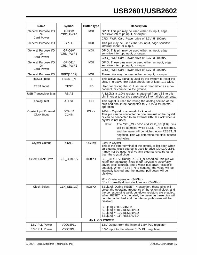
USB2601/USB2602
General Purpose I/OOr
Card Power
GPIO8/CRD_PWR0
I/O8 GPIO: This pin may be used either as input, edge sensitive interrupt input, or output.
CRD_PWR: Card Power drive of 3.3V @ 100mA.
General Purpose I/O GPIO9 I/O8 This pin may be used either as input, edge sensitive interrupt input, or output.
General Purpose I/OOr
Card Power
GPIO10/CRD_PWR1
I/O8 GPIO: This pin may be used either as input, edge sensitive interrupt input, or output.
CRD_PWR: Card Power drive of 3.3V @ 100mA.
General Purpose I/OOr
Card Power
GPIO11/CRD_PWR2
I/O8 GPIO: These pins may be used either as input, edge sensitive interrupt input, or output.
CRD_PWR: Card Power drive of 3.3V @ 200mA.
General Purpose I/O GPIO[15:12] I/O8 These pins may be used either as input, or output.
RESET input RESET_N IS This active low signal is used by the system to reset the chip. The active low pulse should be at least 1s wide.
TEST Input TEST IPD Used for testing the IC. User must treat either as a no-connect, or connect to the ground.
USB Transceiver Bias RBIAS I A 12.0k, 1.0% resistor is attached from VSS to this pin, in order to set the transceiver’s internal bias currents.
Analog Test ATEST AIO This signal is used for testing the analog section of the chip and should be connected to VDDA33 for normal operation.
Crystal Input/External Clock Input
XTAL1/CLKIN
ICLKx 24MHz Crystal or external clock input.This pin can be connected to one terminal of the crystal or can be connected to an external 24MHz clock when a crystal is not used.
Note: The ‘SEL_CLKDRV and CLK_SEL[1:0]’ pinswill be sampled while RESET_N is asserted,and the value will be latched upon RESET_Nnegation. This will determine the clock sourceand value.
Crystal Output XTAL2 OCLKx 24MHz CrystalThis is the other terminal of the crystal, or left open when an external clock source is used to drive XTAL1/CLKIN. It may not be used to drive any external circuitry other than the crystal circuit.
Select Clock Drive SEL_CLKDRV I/O8PD SEL_CLKDRV. During RESET_N assertion, this pin will select the operating clock mode (crystal or externally driven clock source), and a weak pull-down resistor is enabled. When RESET_N is negated, the value will be internally latched and the internal pull-down will be disabled.
‘0’ = Crystal operation (24MHz)‘1’ = Externally driven clock source (24MHz)
Clock Select CLK_SEL[1:0] I/O8PD SEL[1:0]. During RESET_N assertion, these pins will select the operating frequency of the external clock, and the corresponding weak pull-down resistors are enabled. When RESET_N is negated, the value on these pins will be internal latched and the internal pull-downs will be disabled.
SEL[1:0] = ‘00’. 24MHzSEL[1:0] = ‘01’. RESERVEDSEL[1:0] = ‘10’. RESERVEDSEL[1:0] = ‘11’. RESERVED
ANALOG POWER
1.8V PLL Power VDD18PLL 1.8V Output from the internal 1.8V PLL regulator
3.3V PLL Power VDD33PLL 3.3V Input to the internal 1.8V PLL regulator.
Name Symbol Buffer Type Description
2004 - 2016 Microchip Technology Inc. DS00002119A-page 15

USB2601/USB2602
Note 1: Hot-insertion capable card connectors are required for all flash media. It is required for SD connector to haveWrite Protect switch. This allows the chip to detect MMC card.
2: nMCE is normally asserted except when the 8051 is in standby mode.
5.2 Buffer Type Descriptions
3.3V Analog Power VDDA33 3.3v Analog PHY Power
DIGITAL POWER, GROUNDS, and NO CONNECTS
1.8V Digital Core Power
VDD18 +1.8V Core power
All VDD18 pins must be connected together on the circuit board.
3.3v Power & &Voltage Regulator
Input
VDD33 3.3V Power & Regulator Input.
Pin 87 supplies 3.3V power to the internal 1.8V regulator.
Ground VSS Ground Reference
No Connect NC No Connect. No trace or signal should be routed/attached to these pins.
TABLE 5-1: USB2601/USB2602 BUFFER TYPE DESCRIPTIONS
Buffer Description
I Input
IPU Input with internal weak pull-up resistor.
IPD Input with internal weak pull-down resistor.
IS Input with Schmitt trigger
I/O8 Input/Output buffer with 8mA sink and 8mA source.
I/O8PU Input/Output buffer with 8mA sink and 8mA source, with an internal weak pull-up resistor.
I/O8PD Input/Output buffer with 8mA sink and 8mA source, with an internal weak pull-down resistor.
I/O12 Input/Output, 12mA
O8 Output buffer with 8mA sink and 8mA source.
O8PU Output buffer with 8mA sink and 8mA source, with an internal weak pull-up resistor.
O8PD Output buffer with 8mA sink and 8mA source, with an internal weak pull-down resistor.
ICLKx XTAL clock input
OCLKx XTAL clock output
I/O-U Analog Input/Output Defined in USB specification
AIO Analog Input/Output
Name Symbol Buffer Type Description
DS00002119A-page 16 2004 - 2016 Microchip Technology Inc.

USB2601/USB2602
6.0 DC PARAMETERS
6.1 Maximum Ratings
Operating Temperature Range* ...................................................................................................................0oC to +70oC
Storage Temperature Range..................................................................................................................... -55o to +150oC
Lead Temperature Range (soldering, 10 seconds) ...............................................................................................+325oC
Positive Voltage on GPIO3, with respect to Ground ..................................................................................................5.5V
Positive Voltage on any signal pin, with respect to Ground .......................................................................................4.6V
Positive Voltage on XTAL1, with respect to Ground...................................................................................................4.0V
Negative Voltage on GPIO8, 10 & 11, with respect to Ground (see Note 6-2)..........................................................-0.5V
Negative Voltage on any pin, with respect to Ground ...............................................................................................-0.5V
Maximum VDD18, VDD18PLL ......................................................................................................................................+2.5V
Maximum VDD33, VDDA33 .........................................................................................................................................+4.6V
* Stresses above the specified parameters could cause permanent damage to the device. This is a stress rating onlyand functional operation of the device at any other condition above those indicated in the operation sections of thisspecification is not implied.
Note 6-1 When powering this device from laboratory or system power supplies, it is important that the AbsoluteMaximum Ratings not be exceeded or device failure can result. Some power supplies exhibit voltagespikes on their outputs when the AC power is switched on or off. In addition, voltage transients onthe AC power line may appear on the DC output. When this possibility exists, it is suggested that aclamp circuit be used.
Note 6-2 When internal power FET operation of these pins is enabled, these pins may be simultaneouslyshorted to ground or any voltage up to 3.63V indefinitely, without damage to the device as long asVDD33 and VDDA33 are less than 3.63V and TA is less than 70°C.
2004 - 2016 Microchip Technology Inc. DS00002119A-page 17

USB2601/USB2602
6.2 Operating Conditions
Note 6-3 When powering the device, the maximum power supply ramp time should be set at a rate faster than400 micro seconds. This speed is important to ensure that the device resets properly. Measure risetime at 10% and 90%.
Parameter Symbol MIN MAX Units Comments
Operating Temperature TA 0 70 °C *Ambient temperature in still air.
1.8V supply voltage VDD18, VDD18PLL
1.62 1.98 V
3.3V supply voltage VDD33, VDDA33
3.0 3.6 V
3.3V supply rise time tRT 0 400 s (See Figure 6-1, "Supply Rise Time Model")
Voltage on XTAL1 -0.3 VDDA33 V
FIGURE 6-1: SUPPLY RISE TIME MODEL
t10%
10%
90%
Voltage tRT
t90% Time
100%3.3V
VSS
VDD33
DS00002119A-page 18 2004 - 2016 Microchip Technology Inc.

USB2601/USB2602
6.3 DC Electrical Characteristics
Parameter Symbol MIN TYP MAX Units Comments
I,IPU & IPD Type Input Buffer
Low Input Level
High Input Level
Pull Down
Pull Up
VILI
VIHI
PD
PU
2.0
72
58
0.8 V
V
A
A
TTL Levels
IS Type Input Buffer
Low Input Level
High Input Level
Hysteresis
VILI
VIHI
VHYSI
2.0
500
0.8 V
V
mV
TTL Levels
ICLK Input Buffer
Low Input Level
High Input Level
VILCK
VIHCK 2.2
0.4 V
V
Input Leakage(All I and IS buffers)
Low Input Leakage
High Input Leakage
IIL
IIH
-10
-10
+10
+10
A
mA
VIN = 0
VIN = VDD33
O8. O8PU & 08PD Type Buffer
Low Output Level
High Output Level
Output Leakage
Pull Down
Pull Up
VOL
VOH
IOL
PD
PU
VDD33- 0.4
-10
72
58
0.4
+10
V
V
A
A
A
IOL = 8 mA @ VDD33= 3.3V
IOH = -8mA @ VDD33= 3.3V
VIN = 0 to VDD33(Note 6-4)
2004 - 2016 Microchip Technology Inc. DS00002119A-page 19

USB2601/USB2602
I/O8, I/O8PU & I/O8PD Type Buffer
Low Output Level
High Output Level
Output Leakage
Pull Down
Pull Up
VOL
VOH
IOL
PD
PU
VDD33-0.4
-10
72
58
0.4
+10
V
V
µA
µA
µA
IOL = 8 mA @ VDD33= 3.3V
IOH = -8 mA @ VDD33= 3.3V
VIN = 0 to VDD33(Note 6-4)
I/O12 Type Buffer
Low Output Level
High Output Level
Output Leakage
VOL
VOH
IOL
2.4
0.4
+10
V
V
uA
IOL = 12mA @ VDD33 =3.3V
IOH = -4mA @ VDD33 =3.3V
VIN = 0 to VDD33(Note 1)
IO-U(Note 6-5)
Integrated Power FET for GPIO8 & GPIO10
Output Current
Short Circuit Current Limit
On Resistance
Output Voltage Rise Time
IOUT
ISC
RDSON
tDSON
100
140
2.1
800
mA
mA
W
ms
GPIO8, or 10; VdropFET = 0.23V
GPIO8, or 10; VoutFET = 0V
GPIO8, or 10; IFET = 70mA
GPIO8, or 10; CLOAD = 10mF
Parameter Symbol MIN TYP MAX Units Comments
DS00002119A-page 20 2004 - 2016 Microchip Technology Inc.

USB2601/USB2602
Note 6-4 Output leakage is measured with the current pins in high impedance.
Note 6-5 See Appendix A for USB DC electrical characteristics.
Note 6-6 The Maximum power dissipation parameters of the package should not be exceeded
Note 6-7 The assignment of each Integrated Card Power FET to a designated Card Connector is controlledby both firmware and the specific board implementation. Firmware will default to the settings listed inTable 8-1, “GPIO Usage (ROM Rev -01),” on page 25.
Integrated Power FET for GPIO11
Output Current
Short Circuit Current Limit
On Resistance
Output Voltage Rise Time
IOUT
ISC
RDSON
tDSON
200
181
2.1
800
mA
mA
s
GPIO11; VdropFET = 0.46V
GPIO11;VoutFET = 0V
GPIO11; IFET = 70mA
GPIO11; CLOAD = 10F
Supply Current Hub, Card Read-er, Unconfigured
High-Speed HostFull-Speed Host
ICCINITICCINIT
9083
mAmA
Supply Current Configured(High-Speed Host)
3 Ext Ports @HSCard Reader Active
302 mA
Total from all supplies
Supply Current Configured(High-Speed Host)
1 Ext Port @HSCard Reader Active
242 mA
Total from all supplies
Supply Current Configured(Full-Speed Host)
1 Ext Port @ FS/LSCard Reader Active
200 mA
Total from all supplies
Supply CurrentSuspend
ICSBY 298 mA Total from all supplies.
Supply CurrentReset
IRST 91 mA Total from all supplies.
Parameter Symbol MIN TYP MAX Units Comments
2004 - 2016 Microchip Technology Inc. DS00002119A-page 21

USB2601/USB2602
6.4 Capacitance
TA = 25°C; fc = 1MHz; VDD18, VDD18PLL = 1.8V
Limits
Parameter Symbol MIN TYP MAX Unit Test Condition
Clock Input Capacitance CIN 20 pF All pins except USB pins (and pins under test tied to AC ground)
Input Capacitance CIN 10 pF
Output Capacitance COUT 20 pF
DS00002119A-page 22 2004 - 2016 Microchip Technology Inc.

USB2601/USB2602
7.0 PACKAGE INFORMATION
Note 1: Controlling Unit: millimeter.
2: Tolerance on the true position of the leads is ± 0.035 mm maximum.Package body dimensions D1 and E1 do not include the mold protrusion.
3: Maximum mold protrusion is 0.25 mm.
4: Dimension for foot length L measured at the gauge plane 0.25 mm above the seating plane.
5: Details of pin 1 identifier are optional but must be located within the zone indicated.
Note: For the most current package drawings, see the Microchip Packaging Specification at: http://www.microchip.com/packaging.
FIGURE 7-1: USB2601/USB2602 128-Pin TQFP Package, 1.0mm Height, 14mm x 14mm Footprint
TABLE 7-1: USB2601/USB2602 128-PIN TQFP PACKAGE PARAMETERS
MIN Nominal MAX Remarks
A ~ ~ 1.20 Overall Package HeightA1 0.05 ~ 0.15 StandoffA2 0.95 ~ 1.05 Body ThicknessD 15.80 ~ 16.20 X Span
D1 13.80 ~ 14.20 X body SizeE 15.80 ~ 16.20 Y SpanE1 13.80 ~ 14.20 Y body SizeH 0.09 ~ 0.20 Lead Frame ThicknessL 0.45 0.60 0.75 Lead Foot Length
L1 ~ 1.00 ~ Lead Lengthe 0.40 Basic Lead Pitchq 0o ~ 7o Lead Foot AngleW 0.13 0.18 0.23 Lead WidthR1 0.08 ~ ~ Lead Shoulder RadiusR2 0.08 ~ 0.20 Lead Foot Radiusccc ~ ~ 0.08 Coplanarity
2004 - 2016 Microchip Technology Inc. DS00002119A-page 23

USB2601/USB2602
7.1 Package Thermal Specifications
TABLE 7-2: 128-PIN TQFP PACKAGE THERMAL PARAMETERS
Parameter Symbol Value Unit Comments
Thermal Resistance JA 53.1 oC/W From the die to the ambient air
Junction-to-Top-of-Package JT 0.3 oC/W
DS00002119A-page 24 2004 - 2016 Microchip Technology Inc.

2004 - 2016 Microchip Technology Inc. DS00002119A-page 25
USB2601/USB2602
8.0 GPIO USAGE
TABLE 8-1: GPIO USAGE (ROM REV -01)
Name Active Level Symbol Description and Note
GPIO1 H Flash Media Activity LED/xD_Door
Indicates media activity. Media or USB cable must not be removed with LED lit. Also may be used for xD Door functionality.
GPIO2 H EE_CS Serial EE PROM chip select.
GPIO3 H V_BUS USB V bus detect.
GPIO4 H EE_DIN/EE_DOUT/xDID Serial EE PROM input/output and xD Identify.
GPIO5 H HS_IND/SD_CD HS Indicator LED or SD Card Detect Switch input.
GPIO6 H A16/ROMEN A16 address line connect for DFU or debug LED indicator optional.
GPIO7 H EE_CLK/UNCONF_LED
Serial EE PROM clock output or Unconfigured LED.
GPIO8 L MS_PWR_CTRL/CRD_PWR0
Memory Stick Card Power Control, or Internal Power FET0.
GPIO9 L CF_PWR_CTRL CompactFlash Card Power Control.
GPIO10 L SM_PWR_CTRL/CRD_PWR1
SmartMedia Card Power Control, or Internal Power FET1.
GPIO11 L SD/MMC_PWR_CTRL/CRD_PWR2
SD/MMC Card Power Control, or Internal Power FET2.
GPIO12 H MS_ACT_IND/Media Activity
Memory Stick Activity Indicator, or Media Activity LED.
GPIO13 H CF_ACT_IND CompactFlash Activity Indicator.
GPIO14 H SM_ACT_IND SmartMedia Activity Indicator.
GPIO15 H SD/MMC_ACT_IND SD/MMC Activity Indicator.

USB2601/USB2602
DS00002119A-page 26 2004 - 2016 Microchip Technology Inc.
APPENDIX A: DATA SHEET REVISION HISTORY
TABLE A-1: REVISION HISTORY
Revision Section/Figure/Entry Correction
DS00002119A (02-25-16) Replaces previous SMSC version Rev. 1.6 (06-20-08)

2004 - 2016 Microchip Technology Inc. DS00002119A-page 27
USB2601/USB2602
THE MICROCHIP WEB SITE
Microchip provides online support via our WWW site at www.microchip.com. This web site is used as a means to makefiles and information easily available to customers. Accessible by using your favorite Internet browser, the web site con-tains the following information:
• Product Support – Data sheets and errata, application notes and sample programs, design resources, user’s guides and hardware support documents, latest software releases and archived software
• General Technical Support – Frequently Asked Questions (FAQ), technical support requests, online discussion groups, Microchip consultant program member listing
• Business of Microchip – Product selector and ordering guides, latest Microchip press releases, listing of semi-nars and events, listings of Microchip sales offices, distributors and factory representatives
CUSTOMER CHANGE NOTIFICATION SERVICE
Microchip’s customer notification service helps keep customers current on Microchip products. Subscribers will receivee-mail notification whenever there are changes, updates, revisions or errata related to a specified product family ordevelopment tool of interest.
To register, access the Microchip web site at www.microchip.com. Under “Support”, click on “Customer Change Notifi-cation” and follow the registration instructions.
CUSTOMER SUPPORT
Users of Microchip products can receive assistance through several channels:
• Distributor or Representative
• Local Sales Office
• Field Application Engineer (FAE)
• Technical Support
Customers should contact their distributor, representative or field application engineer (FAE) for support. Local salesoffices are also available to help customers. A listing of sales offices and locations is included in the back of this docu-ment.
Technical support is available through the web site at: http://www.microchip.com/support

USB2601/USB2602
DS00002119A-page 28 2004 - 2016 Microchip Technology Inc.
PRODUCT IDENTIFICATION SYSTEM
To order or obtain information, e.g., on pricing or delivery, refer to the factory or the listed sales office.
Device: USB2601, USB2602
Temperature Range:
Blank = 0C to +70C Commercial
Package: NE = 128-pin TQFPNU = 128-pin TQFP
PART NO. [X] XXX
PackageTemperatureRange
Device
[X]
Internal Microchip Code
- -Examples:
USB2601/USB2602-NE-XX128-pin TQFP RoHS Compliant package,Commercial Temp, Tray
USB2601/USB2602-NU-XX128-pin TQFP RoHS Compliant package,Commercial Temp, Tray

2004 - 2016 Microchip Technology Inc. DS00002119A-page 29
USB2601/USB2602
Information contained in this publication regarding device applications and the like is provided only for your convenience and may be super-seded by updates. It is your responsibility to ensure that your application meets with your specifications. MICROCHIP MAKES NO REP-RESENTATIONS OR WARRANTIES OF ANY KIND WHETHER EXPRESS OR IMPLIED, WRITTEN OR ORAL, STATUTORY OROTHERWISE, RELATED TO THE INFORMATION, INCLUDING BUT NOT LIMITED TO ITS CONDITION, QUALITY, PERFORMANCE,MERCHANTABILITY OR FITNESS FOR PURPOSE. Microchip disclaims all liability arising from this information and its use. Use of Micro-chip devices in life support and/or safety applications is entirely at the buyer’s risk, and the buyer agrees to defend, indemnify and holdharmless Microchip from any and all damages, claims, suits, or expenses resulting from such use. No licenses are conveyed, implicitly orotherwise, under any Microchip intellectual property rights unless otherwise stated.
Trademarks
The Microchip name and logo, the Microchip logo, AnyRate, dsPIC, FlashFlex, flexPWR, Heldo, JukeBlox, KeeLoq, KeeLoq logo, Kleer, LANCheck, LINK MD, MediaLB, MOST, MOST logo, MPLAB, OptoLyzer, PIC, PICSTART, PIC32 logo, RightTouch, SpyNIC, SST, SST Logo, SuperFlash and UNI/O are registered trademarks of Microchip Technology Incorporated in the U.S.A. and other countries.
ClockWorks, The Embedded Control Solutions Company, ETHERSYNCH, Hyper Speed Control, HyperLight Load, IntelliMOS, mTouch, Precision Edge, and QUIET-WIRE are registered trademarks of Microchip Technology Incorporated in the U.S.A.
Analog-for-the-Digital Age, Any Capacitor, AnyIn, AnyOut, BodyCom, chipKIT, chipKIT logo, CodeGuard, dsPICDEM, dsPICDEM.net, Dynamic Average Matching, DAM, ECAN, EtherGREEN, In-Circuit Serial Programming, ICSP, Inter-Chip Connectivity, JitterBlocker, KleerNet, KleerNet logo, MiWi, motorBench, MPASM, MPF, MPLAB Certified logo, MPLIB, MPLINK, MultiTRAK, NetDetach, Omniscient Code Generation, PICDEM, PICDEM.net, PICkit, PICtail, PureSilicon, RightTouch logo, REAL ICE, Ripple Blocker, Serial Quad I/O, SQI, SuperSwitcher, SuperSwitcher II, Total Endurance, TSHARC, USBCheck, VariSense, ViewSpan, WiperLock, Wireless DNA, and ZENA are trademarks of Microchip Technology Incorporated in the U.S.A. and other countries.
SQTP is a service mark of Microchip Technology Incorporated in the U.S.A.
Silicon Storage Technology is a registered trademark of Microchip Technology Inc. in other countries.
GestIC is a registered trademarks of Microchip Technology Germany II GmbH & Co. KG, a subsidiary of Microchip Technology Inc., in other countries.
All other trademarks mentioned herein are property of their respective companies.
© 2004 - 2016, Microchip Technology Incorporated, Printed in the U.S.A., All Rights Reserved.
ISBN: 9781522403319
Note the following details of the code protection feature on Microchip devices:
• Microchip products meet the specification contained in their particular Microchip Data Sheet.
• Microchip believes that its family of products is one of the most secure families of its kind on the market today, when used in the intended manner and under normal conditions.
• There are dishonest and possibly illegal methods used to breach the code protection feature. All of these methods, to our knowledge, require using the Microchip products in a manner outside the operating specifications contained in Microchip’s Data Sheets. Most likely, the person doing so is engaged in theft of intellectual property.
• Microchip is willing to work with the customer who is concerned about the integrity of their code.
• Neither Microchip nor any other semiconductor manufacturer can guarantee the security of their code. Code protection does not mean that we are guaranteeing the product as “unbreakable.”
Code protection is constantly evolving. We at Microchip are committed to continuously improving the code protection features of ourproducts. Attempts to break Microchip’s code protection feature may be a violation of the Digital Millennium Copyright Act. If such actsallow unauthorized access to your software or other copyrighted work, you may have a right to sue for relief under that Act.
Microchip received ISO/TS-16949:2009 certification for its worldwide headquarters, design and wafer fabrication facilities in Chandler and Tempe, Arizona; Gresham, Oregon and design centers in California and India. The Company’s quality system processes and procedures are for its PIC® MCUs and dsPIC® DSCs, KEELOQ® code hopping devices, Serial EEPROMs, microperipherals, nonvolatile memory and analog products. In addition, Microchip’s quality system for the design and manufacture of development systems is ISO 9001:2000 certified.
QUALITYMANAGEMENTSYSTEMCERTIFIEDBYDNV
== ISO/TS16949==

2004 - 2016 Microchip Technology Inc. DS00002119A-page 30
AMERICASCorporate Office2355 West Chandler Blvd.Chandler, AZ 85224-6199Tel: 480-792-7200 Fax: 480-792-7277Technical Support: http://www.microchip.com/supportWeb Address: www.microchip.com
AtlantaDuluth, GA Tel: 678-957-9614 Fax: 678-957-1455
Austin, TXTel: 512-257-3370
BostonWestborough, MA Tel: 774-760-0087 Fax: 774-760-0088
ChicagoItasca, IL Tel: 630-285-0071 Fax: 630-285-0075
ClevelandIndependence, OH Tel: 216-447-0464 Fax: 216-447-0643
DallasAddison, TX Tel: 972-818-7423 Fax: 972-818-2924
DetroitNovi, MI Tel: 248-848-4000
Houston, TX Tel: 281-894-5983
IndianapolisNoblesville, IN Tel: 317-773-8323Fax: 317-773-5453
Los AngelesMission Viejo, CA Tel: 949-462-9523 Fax: 949-462-9608
New York, NY Tel: 631-435-6000
San Jose, CA Tel: 408-735-9110
Canada - TorontoTel: 905-673-0699 Fax: 905-673-6509
ASIA/PACIFICAsia Pacific OfficeSuites 3707-14, 37th FloorTower 6, The GatewayHarbour City, Kowloon
Hong KongTel: 852-2943-5100Fax: 852-2401-3431
Australia - SydneyTel: 61-2-9868-6733Fax: 61-2-9868-6755
China - BeijingTel: 86-10-8569-7000 Fax: 86-10-8528-2104
China - ChengduTel: 86-28-8665-5511Fax: 86-28-8665-7889
China - ChongqingTel: 86-23-8980-9588Fax: 86-23-8980-9500
China - DongguanTel: 86-769-8702-9880
China - HangzhouTel: 86-571-8792-8115 Fax: 86-571-8792-8116
China - Hong Kong SARTel: 852-2943-5100 Fax: 852-2401-3431
China - NanjingTel: 86-25-8473-2460Fax: 86-25-8473-2470
China - QingdaoTel: 86-532-8502-7355Fax: 86-532-8502-7205
China - ShanghaiTel: 86-21-5407-5533 Fax: 86-21-5407-5066
China - ShenyangTel: 86-24-2334-2829Fax: 86-24-2334-2393
China - ShenzhenTel: 86-755-8864-2200 Fax: 86-755-8203-1760
China - WuhanTel: 86-27-5980-5300Fax: 86-27-5980-5118
China - XianTel: 86-29-8833-7252Fax: 86-29-8833-7256
ASIA/PACIFICChina - XiamenTel: 86-592-2388138 Fax: 86-592-2388130
China - ZhuhaiTel: 86-756-3210040 Fax: 86-756-3210049
India - BangaloreTel: 91-80-3090-4444 Fax: 91-80-3090-4123
India - New DelhiTel: 91-11-4160-8631Fax: 91-11-4160-8632
India - PuneTel: 91-20-3019-1500
Japan - OsakaTel: 81-6-6152-7160 Fax: 81-6-6152-9310
Japan - TokyoTel: 81-3-6880- 3770 Fax: 81-3-6880-3771
Korea - DaeguTel: 82-53-744-4301Fax: 82-53-744-4302
Korea - SeoulTel: 82-2-554-7200Fax: 82-2-558-5932 or 82-2-558-5934
Malaysia - Kuala LumpurTel: 60-3-6201-9857Fax: 60-3-6201-9859
Malaysia - PenangTel: 60-4-227-8870Fax: 60-4-227-4068
Philippines - ManilaTel: 63-2-634-9065Fax: 63-2-634-9069
SingaporeTel: 65-6334-8870Fax: 65-6334-8850
Taiwan - Hsin ChuTel: 886-3-5778-366Fax: 886-3-5770-955
Taiwan - KaohsiungTel: 886-7-213-7828
Taiwan - TaipeiTel: 886-2-2508-8600 Fax: 886-2-2508-0102
Thailand - BangkokTel: 66-2-694-1351Fax: 66-2-694-1350
EUROPEAustria - WelsTel: 43-7242-2244-39Fax: 43-7242-2244-393
Denmark - CopenhagenTel: 45-4450-2828 Fax: 45-4485-2829
France - ParisTel: 33-1-69-53-63-20 Fax: 33-1-69-30-90-79
Germany - DusseldorfTel: 49-2129-3766400
Germany - KarlsruheTel: 49-721-625370
Germany - MunichTel: 49-89-627-144-0 Fax: 49-89-627-144-44
Italy - Milan Tel: 39-0331-742611 Fax: 39-0331-466781
Italy - VeniceTel: 39-049-7625286
Netherlands - DrunenTel: 31-416-690399 Fax: 31-416-690340
Poland - WarsawTel: 48-22-3325737
Spain - MadridTel: 34-91-708-08-90Fax: 34-91-708-08-91
Sweden - StockholmTel: 46-8-5090-4654
UK - WokinghamTel: 44-118-921-5800Fax: 44-118-921-5820
Worldwide Sales and Service
07/14/15