
(4Marks) s - IETE e-Learning & Networksiete-elan.ac.in/SolnQPDec2015/Sol_D15_DE54_DE104.pdfAnswer:...
19
DE54/DE104 ENGINEERING MATERIALS DEC 2015 © IETE 1 Q.2 a. Explain the effect of temperature on electrical conductivity of metals. (4) Answer: The factors, on which the resistivity of conducting materials depends are:- Temperature: The electrical resistance of most metals increases with increase of temperature while those of semiconductors and electrolytes decreases with increase of temperature. Alloying: Alloying is another factor, which affects the resistivity of a material. By the addition of some impurity to the metal, its resistivity can be changed. Alloys have more resistivity than that of the pure metal. Mechanical stressing: When a material undergoes a mechanical treatment, its resistivity changes due to mechanical distortion of the crystal structure. Age hardening: It increases the resistivity of an alloy. (4Marks) b. What are the factors which affect the resistivity of Electrical materials?(12) Answer: Temperature dependence of electrical resistivity and conductivity in conductors: As the temperature is increased, there is a greater thermal motion in the atoms, which decreases the regularity in the atoms spacing with a consequent decrease in the mobility of the electrons. The resitivity of most of the conductors therefore increases with an increase in the temperature. Since the number and the energy of the electrons at top of the Fermi distribution curve vary insignificantly with temperature, the change in temperature must be associated with a change in the mean free path. In a perfectly regular lattice, each electron will exist in a particular energy state and will have a fixed velocity. Practically metals do not have a perfect lattice because of impurities and because of deviations of the atoms about their mean positions due to lattice oscillations. Since the lattice oscillations decreases at low temperature the scattering of electron waves falls and the conductivity therefore increases rapidly as the temperature reaches absolute zero. There is a limiting value beyond which the conductivity will not increase. In general, purer the specimen higher is the conductivity. the conductivity of many conductors decreases linearly as the temperature is increased above the room temperature but below this temperature the conductivity increases markedly.(4 Marks) or Qo= CoV, where Co is defined as the capacitance. By applying gauss theorem the magnitude of the flux density D with the parallel plates is given by D=Qo/A since the electric field strength E is related to the flux density by the relation .(4 Marks) D= OE, the field strength in the region between the plates is given by E=D/Eo = Qo/AEo. Since V=Ed, the capacitance of the system is given by Co=Eo A/d where Eo is termed as the absolute permittivity of free space and is expressed in farads meter. The value of Eo can be determined from experiment and is its value is nearly equal to 10-9/36λ if the space between the plates is now filled with a dielectric and V is kept constant, it is found that the value of charge is found that the value of charge is in reused to a value given by Q=cv hence the new capacitance is given by C=E A/d where E is defined As the absolute permittivity of the dielectric and the ratio is called the relative permittivity or the dielectric constant of the materials. (4Marks) Q.3 a. Explain effects of internal fields in solids and liquids. (12) Answer:
Transcript of (4Marks) s - IETE e-Learning & Networksiete-elan.ac.in/SolnQPDec2015/Sol_D15_DE54_DE104.pdfAnswer:...
DE54/DE104 ENGINEERING MATERIALS DEC 2015
© IETE 1
Q.2 a. Explain the effect of temperature on electrical conductivity of metals. (4) Answer:
The factors, on which the resistivity of conducting materials depends are:- Temperature: The electrical resistance of most metals increases with increase of temperature while those of semiconductors and electrolytes decreases with increase of temperature. Alloying: Alloying is another factor, which affects the resistivity of a material. By the addition of some impurity to the metal, its resistivity can be changed. Alloys have more resistivity than that of the pure metal. Mechanical stressing: When a material undergoes a mechanical treatment, its resistivity changes due to mechanical distortion of the crystal structure. Age hardening: It increases the resistivity of an alloy. (4Marks)
b. What are the factors which affect the resistivity of Electrical materials?(12) Answer:
Temperature dependence of electrical resistivity and conductivity in conductors: As the temperature is increased, there is a greater thermal motion in the atoms, which decreases the regularity in the atoms spacing with a consequent decrease in the mobility of the electrons. The resitivity of most of the conductors therefore increases with an increase in the temperature. Since the number and the energy of the electrons at top of the Fermi distribution curve vary insignificantly with temperature, the change in temperature must be associated with a change in the mean free path. In a perfectly regular lattice, each electron will exist in a particular energy state and will have a fixed velocity. Practically metals do not have a perfect lattice because of impurities and because of deviations of the atoms about their mean positions due to lattice oscillations. Since the lattice oscillations decreases at low temperature the scattering of electron waves falls and the conductivity therefore increases rapidly as the temperature reaches absolute zero. There is a limiting value beyond which the conductivity will not increase. In general, purer the specimen higher is the conductivity. the conductivity of many conductors decreases linearly as the temperature is increased above the room temperature but below this temperature the conductivity increases markedly.(4 Marks)
or Qo= CoV, where Co is defined as the capacitance. By applying gauss theorem the magnitude of the flux density D with the parallel plates is given by
D=Qo/A since the electric field strength E is related to the flux density by the relation .(4 Marks)
D= OE, the field strength in the region between the plates is given by E=D/Eo = Qo/AEo. Since V=Ed, the capacitance of the system is given by Co=Eo A/d where Eo is termed as the absolute permittivity of free space and is expressed in farads meter. The value of Eo can be determined from experiment and is its value is nearly equal to 10-9/36λ if the space between the plates is now filled with a dielectric and V is kept constant, it is found that the value of charge is found that the value of charge is in reused to a value given by Q=cv hence the new capacitance is given by C=E A/d where E is defined As the absolute permittivity of the dielectric and the ratio is called the relative permittivity or the dielectric constant of the materials. (4Marks)
Q.3 a. Explain effects of internal fields in solids and liquids. (12) Answer:

DE54/DE104 ENGINEERING MATERIALS DEC 2015
© IETE 2

DE54/DE104 ENGINEERING MATERIALS DEC 2015
© IETE 3

DE54/DE104 ENGINEERING MATERIALS DEC 2015
© IETE 4

DE54/DE104 ENGINEERING MATERIALS DEC 2015
© IETE 5
b. Explain the effect of dielectric on the behaviour of a capacitor. (4) Answer:
Effect of dialectic on the behavior of a capacitor: Suppose that two large plane parallel plates separated by a distance d(meter) in vaccume are maintained at a potential difference V. the plates will become charged positively and negatively with charges ≠Qo and a uniform electric field with intensity E=v/d will be created between the plates. The magnitude of the charge accumulated on each plate is proportional to the applied p.d, i.e. VQ∞0
00∈∈==∈ccr (4Marks)
Q.4 a. Explain properties and application of polymers. (10) Answer:
Properties & application of Polymers: Polymeric materials or plastics comprise a large group of organic or oregano metallic high molecules compound. (2Marks) The common properties of these materials are their ability to soften and even melt, ability to pass into a liquid state, insolubility in water and solubility in one or more organic solvents. The mechanical properties of these materials vary widely, some can be spun into fibers like nylon and terrylene , other

DE54/DE104 ENGINEERING MATERIALS DEC 2015
© IETE 6
can be moulded and are hard and glass like in mechanical properties. Other group shows rubber like properties. (2Marks) Plastic are synthetic resins obtained basically in two different ways, by linear polymerization and by polycondensation. The polymers obtained by linear polymerization are known as thermoplastics since they can be repeatedly melted or dissolved in various solvents. The properties of the thermoplastics do not change considerably if they are melted and then cooled and solidified. Example of thermoplastics is polystyrene. (3Marks) Second types of polymers are thermosetting and are used as binding agents and varnish base. Thermosetting plastic melt on heating but are converted into a rigid solid mass if maintained at an elevated temperature. Examples of these polymer is phenol formaldehyde. Synthetic resins are widely used in electrical industry as insulating and structural components. Some of the important synthetic resins commonly used in electrical engineering are polystyrenes, P.V.C.(polyvinyl chloride.) etc. (3Marks)
b. Explain the term dielectric losses and dielectric constant. (6) Answer:
Dielectric Loss When an insulating material is subjected to an alternating voltage except in the caseof purified gas as an insulator, there is some consumption of power due to flow of small amount of leakage current. This loss is called dialectic loss. Dielectric loss increases with increase in applied voltage and frequency. Dielectric Constant Every insulation material has the capacity to store charge when placed in between two conducting plates as in capacitors. Relative permittivity or dielectric constant, it is the ratio of the capacitance of a capacitors with a specified dielectric material placed between the plates, to the capacitance of the same capacitor with free space i.e. air between the plates.
Q.5 Discuss the following: (4×4)
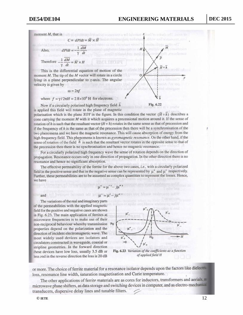
(i) Paramagnetism (ii) Ferromagnetism (iii) Hysteresis loop (iv) Magnetic resonance Answer:

DE54/DE104 ENGINEERING MATERIALS DEC 2015
© IETE 7

DE54/DE104 ENGINEERING MATERIALS DEC 2015
© IETE 8

DE54/DE104 ENGINEERING MATERIALS DEC 2015
© IETE 9

DE54/DE104 ENGINEERING MATERIALS DEC 2015
© IETE 10

DE54/DE104 ENGINEERING MATERIALS DEC 2015
© IETE 11
DE54/DE104 ENGINEERING MATERIALS DEC 2015
© IETE 12

DE54/DE104 ENGINEERING MATERIALS DEC 2015
© IETE 13
Q.6 a. Discuss the following: (5+5)
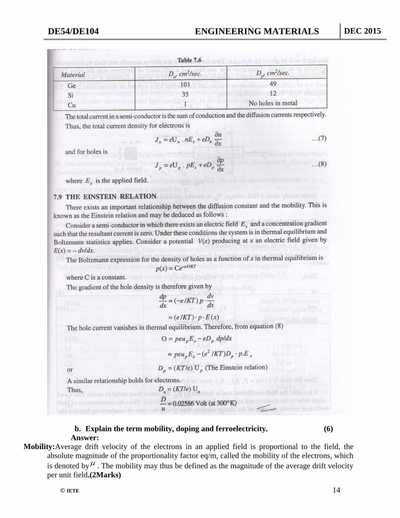
(i) Diffusion in semi conductors (ii) Einstein Relation in semi conductors Answer:
DE54/DE104 ENGINEERING MATERIALS DEC 2015
© IETE 14
b. Explain the term mobility, doping and ferroelectricity. (6) Answer:
Mobility:Average drift velocity of the electrons in an applied field is proportional to the field, the absolute magnitude of the proportionality factor eq/m, called the mobility of the electrons, which is denoted byµ . The mobility may thus be defined as the magnitude of the average drift velocity per unit field.(2Marks)
DE54/DE104 ENGINEERING MATERIALS DEC 2015
© IETE 15
The mobility of the electrons can be determined by knowing the conductivity of the material and estimating the number of free electrons. Unit of mobility is m²/volt.sec.
Doping: Semiconductors in its extremely pure form are called intrinsic semiconductor These intrinsic semiconductor to which some suitable impurity is added in extremely small amount are called extrinsic semiconductor. This process is called doping and impurities are called doping agent. Usually the doping agents are pentavalent atom such as arsenic, antimony or trivalent atom such as gallium, indium, aluminium etc. (2Marks) Ferroelectricity: Ferroelectric materials have a high dielectric constant, which is non linear I.e. it depends to a considerable extent on the intensity of the electric field such materials exhibit hysterisis loops, I.e. the polarization is not a linear function of the applied electric field. If the center of gravity of the positive and the negative charges in a body does not coincide in the absence of an applied electric field, the substance has an electric dipole moment and is said to be spontaneously polarized. Such a substance is called ferroelectrics and the phenomenon is called Ferro electricity. It contains small regions, which are polarized in different directions, even in the absence of an electric field. When the temperature exceeds a certain value called the curie point, the substance looses its ferroelectrics properties. Ex: Rochelle salt, potassium dihydrogen phosphate, barium titan ate.μ (2Marks)
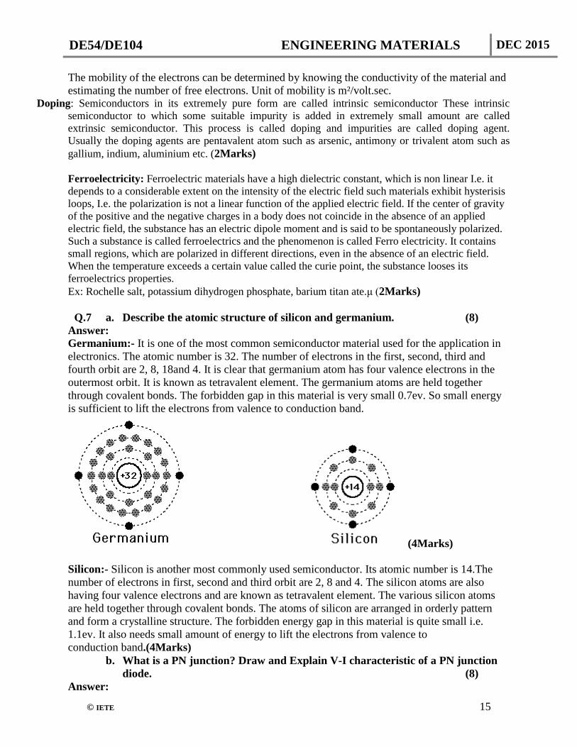
Q.7 a. Describe the atomic structure of silicon and germanium. (8) Answer: Germanium:- It is one of the most common semiconductor material used for the application in electronics. The atomic number is 32. The number of electrons in the first, second, third and fourth orbit are 2, 8, 18and 4. It is clear that germanium atom has four valence electrons in the outermost orbit. It is known as tetravalent element. The germanium atoms are held together through covalent bonds. The forbidden gap in this material is very small 0.7ev. So small energy is sufficient to lift the electrons from valence to conduction band.
(4Marks) Silicon:- Silicon is another most commonly used semiconductor. Its atomic number is 14.The number of electrons in first, second and third orbit are 2, 8 and 4. The silicon atoms are also having four valence electrons and are known as tetravalent element. The various silicon atoms are held together through covalent bonds. The atoms of silicon are arranged in orderly pattern and form a crystalline structure. The forbidden energy gap in this material is quite small i.e. 1.1ev. It also needs small amount of energy to lift the electrons from valence to conduction band.(4Marks) b. What is a PN junction? Draw and Explain V-I characteristic of a PN junction
diode. (8) Answer:

DE54/DE104 ENGINEERING MATERIALS DEC 2015
© IETE 16
P-N junction: When a p-type semiconductor is suitably joined to an n-type semiconductor the contact surface so formed is called p-n junction. All the semiconductor devices contain one or more p-n junction. P-N junction is fabricated by special techniques namely growing, alloying and diffusion methods. The p-type semiconductor is having negative acceptor ion and holes. The n-type semiconductor is having positive donor ions and negatively charged electrons. When the two pieces are joined together and suitably treated they form a p-n junction. (3Marks)
(3 Marks) The leakage current for reasonable voltages in the reverse direction ranges between 0.01 and 1 μA depending on the semiconductor material and the doping level of the impurities. Several variations of this simple diode have been developed. (2Marks)
Q.8 a. What is Metal Oxide film resistor? Explain in brief. (6) Answer: Metallic –Oxide Film Resisors When a solution of stannic chloride is sprayed on to a glass or
porcelain at red heat, hydrolysis takes place and yields a glass –like layer of oxide. This layer may vary in thickness from a few hundred to many thousands of angstrom units, has a milky, translucent appearance and is electrically conducting. Additions of antimony trichloride to the spraying solution impart a blue color to the oxide layer. No film will be produced with pure antimony trichloride solution. Oxide films obtained by this process are hard, adherent to glass and ceramics and unaffected by chemical reagents. Besides the electrical resistance can be varied over a wide range of value by changing the composition of spraying solution. Usually films which have comparatively small temperature coefficients of resistance and small resistivities are used. The following are some of the advantages of oxide-film resistors. 1. No oxidation. 2. Soldering of end connections is comparatively easy 3. Maximum temperature ratings higher than that for carbon. 4. Reasonably low temperature- coefficient. (6Marks)
b. Write the properties of ceramic dielectric capacitor and electrolytic capacitors. Write at least two applications of each. (10)
Answer:

DE54/DE104 ENGINEERING MATERIALS DEC 2015
© IETE 17

DE54/DE104 ENGINEERING MATERIALS DEC 2015
© IETE 18
Q.9 a. Give general properties of Field Effect Transistor (FET). (8) Answer: This class of transistors may be distinguished from solid state devices by several features which are common to all members of the class: Flow of carriers in a particular device is controlled by the application of an electric field which permeates into the main conduction path in a semiconductor; this gives rise to the term field effect. (4Marks)

DE54/DE104 ENGINEERING MATERIALS DEC 2015
© IETE 19
Current flow along the main conduction path is almost entirely due to the motion of majority carriers, injection of minority carriers, a mechanism which is essential for the operation of the bipolar transistor is not a necessary requirement in field effect devices. The generic term unipolar is therefore used as an alternative to field effect to describe the devices since they rely only on one type of carrier for current transport. (4Marks) b. Discuses epitaxial diffused junction diode and its application. (8) Answer: Such diodes are now being manufactured commercially on a large scale. The process involve the growing of a thin layer of single crystal semiconductor onto a supporting slice of parent material. The basic chemical reaction of silicon chloride in an atmosphere of H2 at around 12000C, Doped impurity layers and even compound semiconductors can be deposited by similar techniques. For discrete diodes, the parent slice called the substrate is highly doped to give it a low receptivity and the epitaxial layer lightly doped with the same impurity type. A pn junction is then formed in the layer and electrodes are deposited by the same processes that are used for diffused diodes. Diodes with high break down voltage and low capacitance can be fabricated in this way in the high resistivity. Epitaxial layer, while the low resistance supporting substrate reduces the series resistance of the diode. (4+4 Marks)
Text Book Introduction to Electrical Engineering Materials by C S Indulkar and S
Thiruvengadam, 4th Edition , Reprint 2006 edition, S Chand and Company, New Delhi.


![AE71/AC67/AT67 DATA COMM. & COMPUTER NETWORKS DEC …iete-elan.ac.in/SolnQPDec2015/Sol_D15_AE71-AC67-AT67.pdf · officially MAC bridge[1]) is a computer networking device that connects](https://static.fdocuments.in/doc/165x107/5edc0dcdad6a402d66668e7b/ae71ac67at67-data-comm-computer-networks-dec-iete-elanacinsolnqpdec2015sold15ae71-ac67-at67pdf.jpg)

