4H-SiC MOSFETs with: (i) Phosphosilicateglass gate ...neil/SiC_Workshop... · 900C PSG 1000C PSG...
37
C. Jiao, Y. Zheng, A. Modic, T. –I. Smith, A. C. Ahyi and S. Dhar Dept. of Physics, Auburn University, Auburn, AL, USA 4H-SiC MOSFETs with: (i) Phosphosilicate glass gate dielectric (ii) Surface counter-doping with Sb 10 th ARL SiC MOS Workshop, College Park, MD, Aug 13, 2015
Transcript of 4H-SiC MOSFETs with: (i) Phosphosilicateglass gate ...neil/SiC_Workshop... · 900C PSG 1000C PSG...
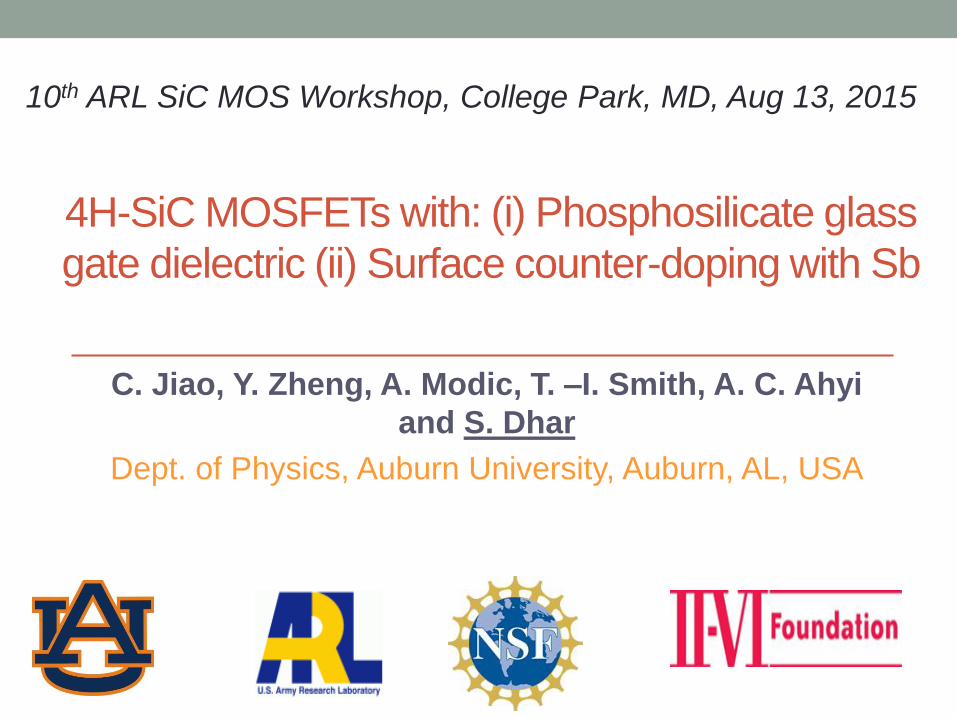
C. Jiao, Y. Zheng, A. Modic, T. –I. Smith, A. C. Ahyi
and S. Dhar
Dept. of Physics, Auburn University, Auburn, AL, USA
4H-SiC MOSFETs with: (i) Phosphosilicate glass
gate dielectric (ii) Surface counter-doping with Sb
10th ARL SiC MOS Workshop, College Park, MD, Aug 13, 2015
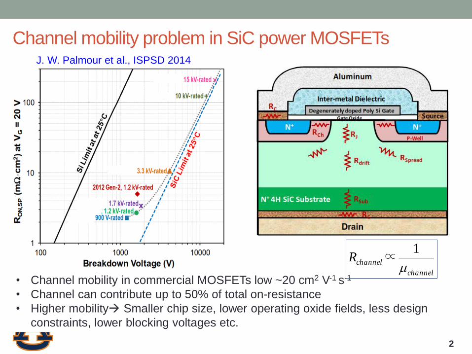
Channel mobility problem in SiC power MOSFETs
2
• Channel mobility in commercial MOSFETs low ~20 cm2 V-1 s-1
• Channel can contribute up to 50% of total on-resistance
• Higher mobility Smaller chip size, lower operating oxide fields, less design
constraints, lower blocking voltages etc.
channel
channelR
1∝
J. W. Palmour et al., ISPSD 2014
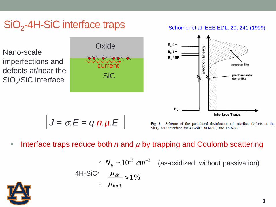
SiO2-4H-SiC interface traps
3
Interface traps reduce both n and by trapping and Coulomb scattering
4H-SiC%1
bulk
ch
Nano-scale
imperfections and
defects at/near the
SiO2/SiC interface
Oxide
SiC
current
J = .E = q.n.µ.E
21310~ cmNit (as-oxidized, without passivation)
3
Schorner et al IEEE EDL, 20, 241 (1999)

0 5 10 15 20
0.0
5.0x10¹²
1.0x10¹³
Experiment
Model
Ele
ctr
on c
oncentr
ation (
cm
-2)
Gate Voltage (V)
Ideal model
Slope=Cox/q
Measured
slope≈Cox/q
1175C NO
annealing, tox=
550 A
4
Interface trap passivation
Ele
ctr
on d
ensity (
10
12 c
m-2
)
Gate Voltage (V)
Ideal model
Slope=Cox/q
Measured
Slope<<Cox/q
E. Arnold et al. IEEE Trans. Elec. Dev (2001)
• As-ox: >90% free e- remain
trapped 4
Cox= SiO2
capacitance
S. Dhar et al. Jn. Appl. Physics (2010)
• NO: Reduction of trap density:
>1013 cm-2 ~1012 cm-2
As-oxidized NO annealed

Si MOSFET: ‘Universal’ mobility behavior
5
Takagi et al.,IEEE TED, 12, 2357 (1994)
• Low electron density n:
Coulomb scattering
• Moderate n, moderate
temperature: Phonon
scattering
• High n: Surface
roughness scattering
1/ch= 1/phonon + 1/coulomb +1/SR

Mobility in NO annealed 4H-SiC MOSFET
6
50 100 150 200 250 300 350 400 45010
15
20
25
30
35
40
45
Ha
ll M
ob
ility
(cm
2 V
-1 s
-1)
Temperature (K)
ns: 7.4E11 cm
-2
ns: 1.4E12 cm
-2
ns: 4.0E12 cm
-2
ns: 5.0E12 cm
-2
T1
n increasing
No ndependence
Regime 1 Regime 2
S. Dhar et al., ICSCRM (2011) T< 373 K, T µ
• Coulomb
scattering
• Thermally
activated
transport
T >400 K, T µ
• Coulomb
scattering at low
fields
• Phonon and
surface
roughness
scattering at
high E fields
1175C NO
tox= 550 A

Summary of 4H-SiC MOS interface treatments
7
• Group I :
• Hydrogen/wet anneals: μ> 200 cm2 V-1s-1 Si-face, weakly bonded, instability
• Na, K: μ~ 200 cm2 V-1s-1 , heavy instability
(mid 2000s, Chalmers Univ., Sweden)
• Cs, Rb: μ~ 40 cm2 V-1s-1 , high Dit ,
Lichtenwalner et al., Appl Phys Lett. (2014)
• Group II: Alkaline earth metals
• Ca, Ba, Sr (oxide interlayers): μ~ 90 cm2 V-1s-1 , low Dit,
Lichtenwalner et al., Appl Phys Lett. (2014)
• Group III:
• B (Borosilicate glass): μ~ 100 cm2 V-1s-1 , low Dit,
Okamoto et al., IEEE EDL, (2014)
• Group V:
• N (Various processes): μ~ 35 cm2 V-1s-1 , low Dit , most reliable oxide
Most widely studied SiC MOS system 2000-2014
• P (Phosphoslicate glass): μ~ 100 cm2 V-1s-1 , low Dit , poor long term stability
Okamoto et al., IEEE EDL, (2010)
• Sb (surface doping) + N: μ~ 100 cm2 V-1s-1 , low Dit , technologically promising
Modic et al., IEEE EDL, (2014)
THIS TALK

Scaling between interface trap density and mobility
1/ch= 1/phonon + 1/coulomb +1/SR
0 2 4 6 8 10 12 140
10
20
30
40
50
60
70
80
90
Max. m
obili
ty (
cm
2V
-1s-1
)
No. of interface traps (1011
cm -2)
Phospho-silicate glass (PSG)
‘Thin PSG’
N3 =Standard NO
NO + H
N0
N4
N1N2
• NO annealing: Most
established trap
passivation method
• scales with number of
interface traps (Rozen et al.
IEEE TED, 2011)
• Trapping and Coulomb
scattering limited at low
gate voltages
8

Recent Results: Non-scaling between trapping and mobility
0 2 4 6 8 10 12 140
20
40
60
80
100
120
140
Max. m
obili
ty (
cm
2V
-1s
-1)
No. of interface traps (1011
cm -2)
PSG (a-face)
PSG process A
NO (a-face)
N plasma (Si-face)
• Surface counter
doping by N and P
• Inaccurate Dit
measurements as
‘fast traps’ not
included. (Yoshioka
et al. , J. Appl.
Phys., 2012)
1/ch= 1/phonon + 1/coulomb + 1/SR
9
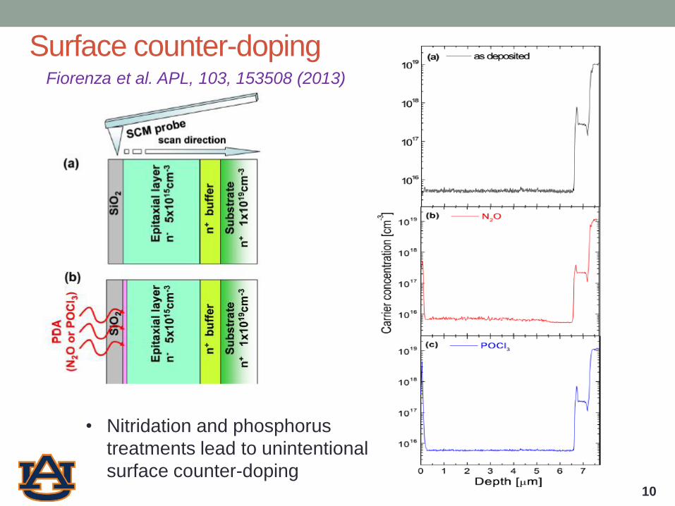
Surface counter-dopingFiorenza et al. APL, 103, 153508 (2013)
• Nitridation and phosphorus
treatments lead to unintentional
surface counter-doping 10

‘Fast states’ and the C-ψs method
11
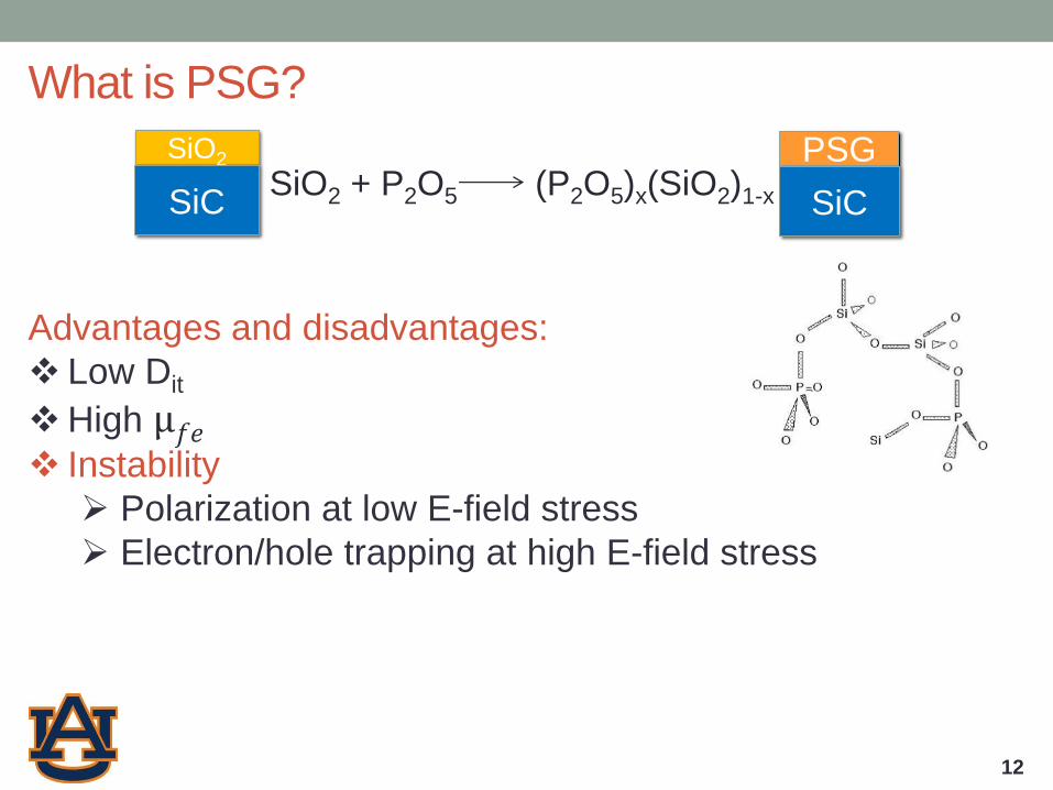
What is PSG?
12
SiO2
SiC
PSG
SiCSiO2 + P2O5 (P2O5)x(SiO2)1-x
Advantages and disadvantages:
Low Dit
High µ𝑓𝑒 Instability
Polarization at low E-field stress
Electron/hole trapping at high E-field stress

Phosphosilicate glass (PSG) formation process
13
4POCl3 + 3O2 2P2O5 + 6Cl2Condition:
Maintain POCl3 at 15°C; bubble through by N2;
Anneal at 900~1100°C (15min) flowing O2;
Post anneal (drive-in, 30min) with N2 at same temperature as annealing.
Allows the study of annealing temperature variation
900~1100°C

Phosphorus uptake with temperature variation
14
0
1
2
3
4
5
6
7
0
0.2
0.4
0.6
0.8
1
1.2
1.4
1.6
1.8
900 950 1000 1050 1100
P interface coverage
P bulk percentage
P in
terf
ace
co
vera
ge (
10
14
cm-2
)
Annealing T (°C)
Courtesy: C. Xu and L.C. Feldman, Rutgers Univ.

15
Reason for different P uptake
POCl3temp
Bulk P
percent (%)
x value
900°C 6.7 0.115
950°C 5.2 0.087
1000°C 4.6 0.076
1050°C 4.6 0.076
1100°C 4.2 0.069
During the drive-in annealing, some
P2O5 is lost to the gas phase by
evaporation.
(P2O5)x (SiO2)1-x
Reference: P. Balk and J.M. Eldridge,
“Phosphosilicate Glass Stabilization of FET
devices”, IEEE, 1969

C-ψs characterization
16
Courtesy: C-ψs code provided by D. Morisette, Purdue Univ.
Taking ‘fast states’
into account, higher
P coverage leads to
lower Dit1E+09
1E+10
1E+11
1E+12
1E+13
0.2 0.3 0.4 0.5 0.6 0.7 0.8
950C PSG
1000C PSG
1100C PSG
Dit
(cm
-2*e
V-1
)
Ec - E (eV)
Interface traps correlation with P coverage

100K100K
17
NOPSG
PSG: Lower density of ‘fast traps’
Wei-Chieh Kao et al., Semiconductor Science and Tech., 2015
Low temperature G-ω measurement

PSG Instability
0.00E+00
2.00E-11
4.00E-11
6.00E-11
8.00E-11
1.00E-10
1.20E-10
1.40E-10
1.60E-10
1.80E-10
-10 -5 0 5 10
d1
d1 5m
Cap
acit
ance
(F)
Voltage (V)
∆V ~ -2.9V
1000 °C PSG
0.00E+00
2.00E-11
4.00E-11
6.00E-11
8.00E-11
1.00E-10
1.20E-10
1.40E-10
1.60E-10
-10 -5 0 5 10
b2
b2 5m
Cap
acit
ance
(F)
Voltage (V)
∆V ~ 0.65V
1100 °C PSG
BTS condition: 150°C, +1.5MV/cm,
5 min
18

Two competing mechanisms of instability:trapping and polarization
BTS: qNnet = q(Ntrp - Npol) = Cox × ∆VFB(1)
Relaxation (20 days): Npol ≈ 0 , qNtrp = Cox × ∆VFB(2)
(assumption: electron trapping relaxes much slower than polarization)
T (°C) Npol (×1012 cm-2) Ntrp(×1012 cm-2)
1000 1.23 0.77
1050 0.40~0.66 0.60~1.45
1100 0.32 0.88
Devices with 1 h BTS:
Polarization scales with phosphorus uptake.
P
19

0
20
40
60
80
100
0 1 2 3 4 5
900C PSG
1000C PSG
1100C PSG
µfe
(cm
2V
-1s
-1)
Eox (MV/cm)
Field-effect mobility µ𝑓𝑒 dependence on P
20
At high E-field,
mobility of 1000°C
PSG is highest.
Possible reason:
Trade-off between
trap passivation and
counter-doping
P-type SiC
N+ N+
Mo Gate
PSGNi Ni
L = 150μm,
W = 290μm

Temperature dependence of mobility: PSG
21
1
µ=
1
µ𝑐+
1
µ𝑠𝑟+
1
µ𝑠𝑝
µ𝑐 : T ↑, µ𝑐 ↑
µ𝑠𝑝 : T ↑, µ𝑠𝑝 ↓
µ𝑠𝑟 : weak T dependence
900 oC PSG
1100 oC PSG

PSG Summary
• POCl3 annealing temperature variation causes different P
interface coverage
• Correlation: higher P coverage results in lower Dit
• Two competing mechanisms of instability identified: trapping
and polarization. Polarization charge scales with P uptake.
• Correlation between P coverage and µ𝑓𝑒 needs further
investigation
• Temperature dependence of µ𝑓𝑒 shows different limiting
mechanisms: Coulomb scattering µ𝑐 and surface roughness
scattering µ𝑠𝑟.
22

Separation of trap passivation and counter-
doping effects
• Difficult to investigate using N or P
as they result in both effects
• Heavier dopants (As, Sb) not
expected to chemically passivate
dangling bonds
• Surface counter-doping with Sb
23
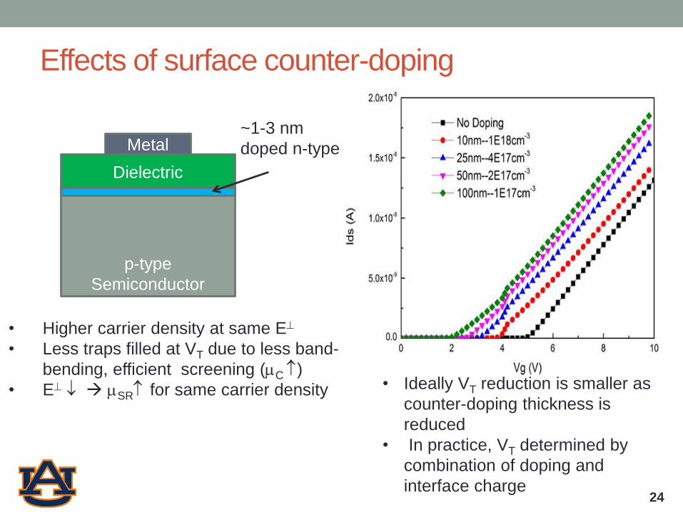
Effects of surface counter-doping
p-type
Semiconductor
Dielectric
Metal~1-3 nm
doped n-type
• Higher carrier density at same E
• Less traps filled at VT due to less band-
bending, efficient screening (C )
• E SR for same carrier density • Ideally VT reduction is smaller as
counter-doping thickness is
reduced
• In practice, VT determined by
combination of doping and
interface charge 24

Sb surface doping processSIMS
25

Sb profile after oxidation
• ~75% of Sb lost during
oxidation
• Total interfacial amount
: ~5.7E12 cm-2
• Total activated
amount:~10%
• Width of profile limited
by depth resolution of
SIMS. Layer < 10 nm
• No crystal damage
detected by ion
scattering
SiCSiO2
FWHM
~10 nm
26
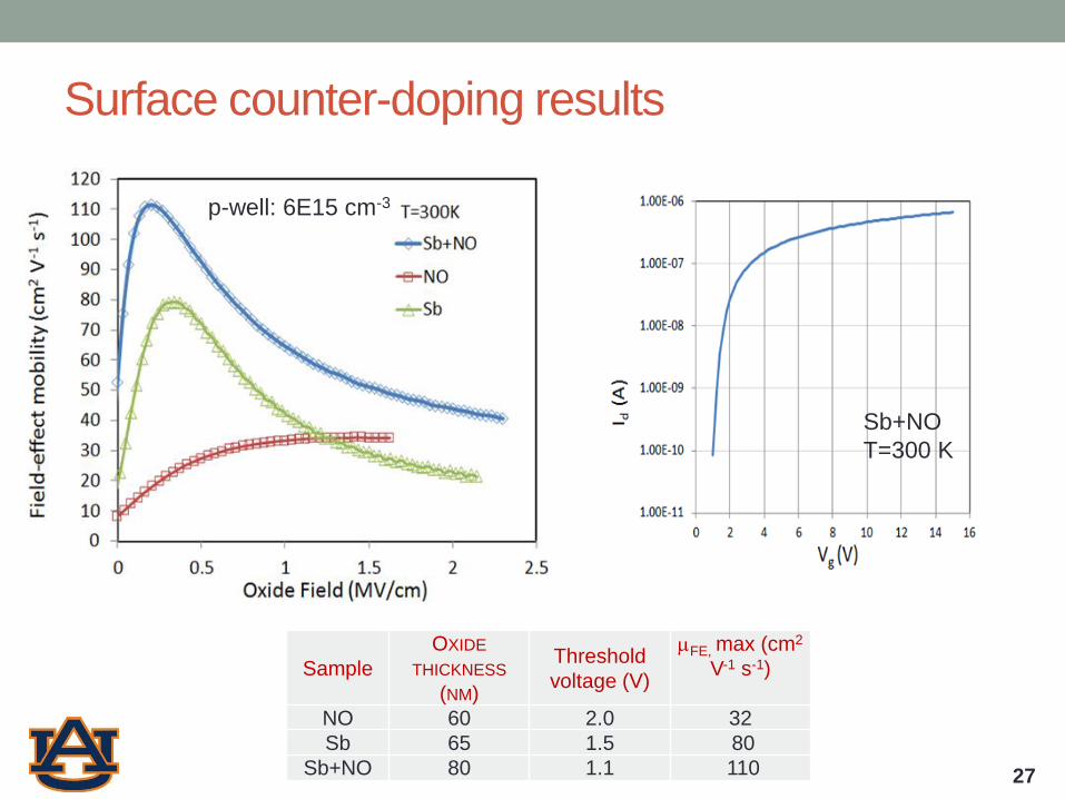
Surface counter-doping results
p-well: 6E15 cm-3
Sb+NO
T=300 K
Sample
OXIDE
THICKNESS
(NM)
Threshold
voltage (V)
FE, max (cm2
V-1 s-1)
NO 60 2.0 32
Sb 65 1.5 80
Sb+NO 80 1.1 110 27

Sb acts as a dopant but does not passivate traps
28
n type
Ec
Ei
EF
Ev
---
V EFn type
Ec
Ei
EF
Ev
----
V EF-
Low temperature High temperature
‘Sb only’ ‘Sb + NO’

Temperature dependence of ‘Sb+NO’ mobility
• Low field performance at high temperature better than NO
• High field performance at higher temperature similar to NO
• Low temperature behavior same as NO

‘Universal’ mobility behavior for NO annealed
interfacesF
E m
obili
ty (
cm
2V
-1 s
-1)

‘Sb+NO’: Threshold voltage stability

32
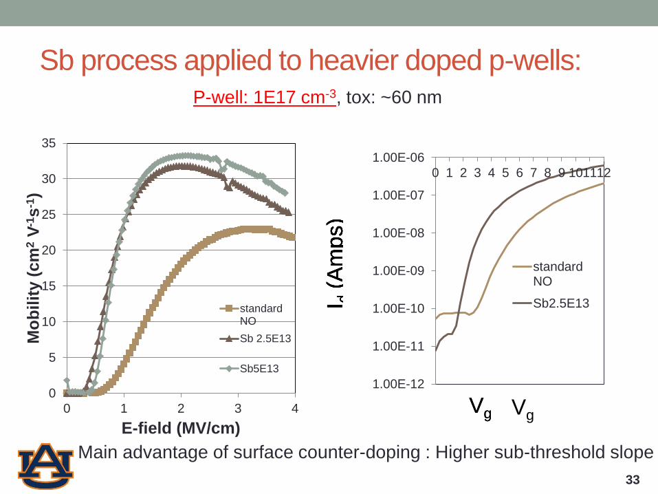
Sb process applied to heavier doped p-wells:
P-body doping Standard NO(no Sb) Sb 2.5E13cm-2 Sb 5E13cm-2
Al 1E17 1 1 1
Al 5E17 1 1 1
Sb
Al
1.00E+15
1.00E+16
1.00E+17
1.00E+18
1.00E+19
1.00E+20
0 500
100
0
150
0
200
0
250
0
300
0
350
0
400
0
450
0
ion
s/c
m3
Range (A)
Al Implant concentration 1e17/cm3: mask Mo 1000 A, SiO2 150 A
Sb, 80 KeV, 2.5e13
Sum Al implant
Oxide ends
33
P-well: 1E17 cm-3, tox: ~60 nm
Sb process applied to heavier doped p-wells:
Main advantage of surface counter-doping : Higher sub-threshold slope
0
5
10
15
20
25
30
35
0 1 2 3 4
Mo
bil
ity (
cm
2V
-1s
-1)
E-field (MV/cm)
standardNO
Sb 2.5E13
Sb5E13
1.00E-12
1.00E-11
1.00E-10
1.00E-09
1.00E-08
1.00E-07
1.00E-06
0 1 2 3 4 5 6 7 8 9 101112
standardNO
Sb2.5E13
Vg
I d(A
mps)
Vg
I d(A
mps)
Vg
I d(A
mps)
I d(A
mps)

34
P-well: 5 E17 cm-3, tox: ~60 nm
Sb process applied to heavier doped p-wells:
• Higher S can be obtained on heavy p-wells
• Process optimization: Uneven activation/loss of Sb

Summary
• Highlights of recent SiC MOS channel engineering results
presented
• Transport limited by ‘fast traps’ and ‘surface roughness’
• Details of these mechanisms not clear
• ‘Universal’ mobility behavior in SiC MOSFETs identified
• PSG is a unique model system to study channel transport
with minimal effects of trapping
• Surface counter-doping processes have strong potential for
threshold voltage control and sub-threshold slope
improvement in practical MOSFETs
35

Acknowledgements• A. C. Ahyi, T.-Isaacs Smith, A.
Modic, C. Jiao, Y. Zheng
(Auburn group)
• G. Liu and L. C. Feldman
(Rutgers University)
• D. Morissette and J.A. Cooper
(Purdue University)
• S.T. Pantelides and group
(Vanderbilt University)
• P. Mooney (Simon Fraser
University)
• M. Goryll (Arizona State)
• R. Kaplar (Sandia)
• A. Lelis (ARL)
36

THANK YOU !!
37