48-Channel Isolated D/I and Relay...
30
PCLD-8751/8761/8762 48-Channel Isolated D/I and Relay Board User Manual
Transcript of 48-Channel Isolated D/I and Relay...

PCLD-8751/8761/8762
48-Channel Isolated D/Iand Relay Board
User Manual
Copyright
The documentation and the software included with this product are copy-righted 2006 by Advantech Co., Ltd. All rights are reserved. Advantech Co., Ltd. reserves the right to make improvements in the products described in this manual at any time without notice. No part of this man-ual may be reproduced, copied, translated or transmitted in any form or by any means without the prior written permission of Advantech Co., Ltd. Information provided in this manual is intended to be accurate and reli-able. However, Advantech Co., Ltd. assumes no responsibility for its use, nor for any infringements of the rights of third parties, which may result from its use.
Acknowledgements
All product names / trademarks are properties of their respective owners.
Part No. 2003876200 1st Edition
Printed in Taiwan August 2006
PCLD-8751/8761/8762 User Manual ii

Product Warranty (2 years)
Advantech warrants to you, the original purchaser, that each of its prod-ucts will be free from defects in materials and workmanship for two years from the date of purchase.
This warranty does not apply to any products which have been repaired or altered by persons other than repair personnel authorized by Advantech, or which have been subject to misuse, abuse, accident or improper instal-lation. Advantech assumes no liability under the terms of this warranty as a consequence of such events.
Because of Advantech’s high quality-control standards and rigorous test-ing, most of our customers never need to use our repair service. If an Advantech product is defective, it will be repaired or replaced at no charge during the warranty period. For out-of-warranty repairs, you will be billed according to the cost of replacement materials, service time and freight. Please consult your dealer for more details.
If you think you have a defective product, follow these steps:
1. Collect all the information about the problem encountered. (For example, CPU speed, Advantech products used, other hardware and software used, etc.) Note anything abnormal and list any onscreen messages you get when the problem occurs.
2. Call your dealer and describe the problem. Please have your man-ual, product, and any helpful information readily available.
3. If your product is diagnosed as defective, obtain an RMA (return merchandize authorization) number from your dealer. This allows us to process your return more quickly.
4. Carefully pack the defective product, a fully-completed Repair and Replacement Order Card and a photocopy proof of purchase date (such as your sales receipt) in a shippable container. A product returned without proof of the purchase date is not eligible for war-ranty service.
5. Write the RMA number visibly on the outside of the package and ship it prepaid to your dealer.
iii

Technical Support and Assistance
Step 1. Visit the Advantech web site at www.advantech.com/support where you can find the latest information about the product.
Step 2. Contact your distributor, sales representative, or Advantech's cus-tomer service center for technical support if you need additional assistance. Please have the following information ready before you call:- Product name and serial number- Description of your peripheral attachments- Description of your software (OS, version, software, etc.)- A complete description of the problem- The exact wording of any error messages
PCLD-8751/8761/8762 User Manual iv

ContentsChapter 1 Introduction ..................................................... 2
1.1 General Information .......................................................... 21.2 Features ............................................................................. 2
Table 1.1:PCLD-8751/8761/8762 Channel Information 2
Chapter 2 Installation ....................................................... 42.1 Initial Inspection................................................................ 4
2.1.1 Caution! ........................................................................ 42.2 Connectors and Jumpers.................................................... 5
Chapter 3 Operations...................................................... 183.1 Power Source Selection................................................... 183.2 Control Logic .................................................................. 183.3 Wiring.............................................................................. 19
3.3.1 Isolated DI .................................................................... 19
Appendix A Specifications ................................................. 22A.1 Isolated Digital Input....................................................... 22A.2 Relay Output ................................................................... 22A.3 General ............................................................................ 23
v

PCLD-8751/8761/8762 User Manual vi

2
CH
AP
TE
R
1
Introduction
This chapter introduces PCLD-8751, PCLD-8761, and PCLD-8762.
Sections include:
• General Information
• Features
PCLD-8751/8761/8762 User Manual 2
Chapter 1 Introduction
1.1 General Information
PCLD-8751, PCLD-8761 and PCLD-8762 are daughter boards that fea-ture 48 isolated digital input/relay output channels. They can only be used by Advantech’s TTL DI/O cards with a 68-pin SCSI connector (PCI-1751 and PCI-1753 series).
In addition to onboard screw terminals for easy wiring, each channel is equipped with an LED to indicate the status. If the input voltage level is high or the output channel is activated, the LED will be lit, otherwise the LED is off. You may configure the channels to work in either positive logic mode or negative logic mode by setting the onboard jumpers.
1.2 Features
• Works with Advantech TTL DI/O cards equipped with 48 digital input/output channels on SCSI 68-pin cable connectors
• 48 opto-isolated digital input/ relay output channels
• Detachable screw terminal for easy wiring
• LEDs indicate input/output logic status
Table 1.1: PCLD-8751/8761/8762 Channel Information
Module PCLD-8751 PCLD-8761 PCLD-8762
Isolated DI Channels 48 24 N/A
Relay Output Channels N/A 24 48

2
CH
AP
TE
R
2
Installation
This chapter show how to install and configure PCLD-8751, PCLD-8761 & PCLD-8762.
Sections include:
• Initial Inspection
• Connectors and Jumpers
Chapter 2 Installation
2.1 Initial Inspection
PCLD-8751, PCLD-8761 & PCLD-8762 are thoroughly inspected before being shipped. Before installing the board, make sure that everything has been included in the package. You should also inspect the board for any defects or damage that may have occurred during shipping. If you find anything missing, defective or damaged, contact your dealer immediately.
2.1.1 Caution!
The board should be handled by the edges only. Static electric discharge can damage the integrated circuits on the board
Packing List
• 1 * PCLD-8751, PCLD-8761 or PCLD-8762.
• 1 * User Manual
Remove the board from its protective packaging. Keep the packaging, since it may be used to return the card if it needs repairs. The packaging may also be used if the card is to be stored for any length of time.
PCLD-8751/8761/8762 User Manual 4
2.2 Connectors and Jumpers
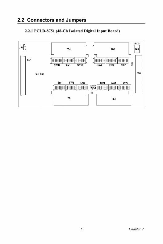
2.2.1 PCLD-8751 (48-Ch Isolated Digital Input Board)
5 Chapter 2

CN1: SCSI 68-pin Connector
PCLD-8751/8761/8762 User Manual 6

TB1/TB2/TB3/TB4: Wiring Terminal Block
TB5: External Power Source Connector
External power source connector for Dry contact mode isolation input channels. When using Dry contact input mode, it is necessary to provide external power through TB5. The voltage range is +5V ~ 30V DC.
TB6: Reserved for the Counter Function on PCI-1751/PCI-1751U
SW1~SW12: Wet/Dry Contact Selection
SW1 ~ SW12 are used to switch the input channels as “Wet Contact” or “Dry Contact”. The factory settings of the switches are in “Off” position, and the input channels are in Wet contact mode.
You can set each input channel as Dry contact mode by setting the switch to the “On” position. Following is the mapping table of the DIP switch and the input channels.
TB1 TB2 TB3 TB4
Name Pin Name Pin Name Pin Name Pin
PA00 1+,1- PB04 13+,13- PA10 25+,25- PB14 37+,37-
PA01 2+,2- PB05 14+,14- PA11 26+,26- PB15 38+,38-
PA02 3+,3- PB06 15+,15- PA12 27+,27- PB16 39+,39-
PA03 4+,4- PB07 16+,16- PA13 28+,28- PB17 40+,40-
PA04 5+,5- PC00 17+,17- PA14 29+,29- PC10 41+,41-
PA05 6+,6- PC01 18+,18- PA15 30+,30- PC11 42+,42-
PA06 7+,7- PC02 19+,19- PA16 31+,31- PC12 43+,43-
PA07 8+,8- PC03 20+,20- PA17 32+,32- PC13 44+,44-
PB00 9+,9- PC04 21+,21- PB10 33+,33- PC14 45+,45-
PB01 10+,10- PC05 22+,22- PB11 34+,34- PC15 46+,46-
PB02 11+,11- PC06 23+,23- PB12 35+,35- PC16 47+,47-
PB03 12+,12- PC07 24+,24- PB13 36+,36- PC17 48+,48-
7 Chapter 2
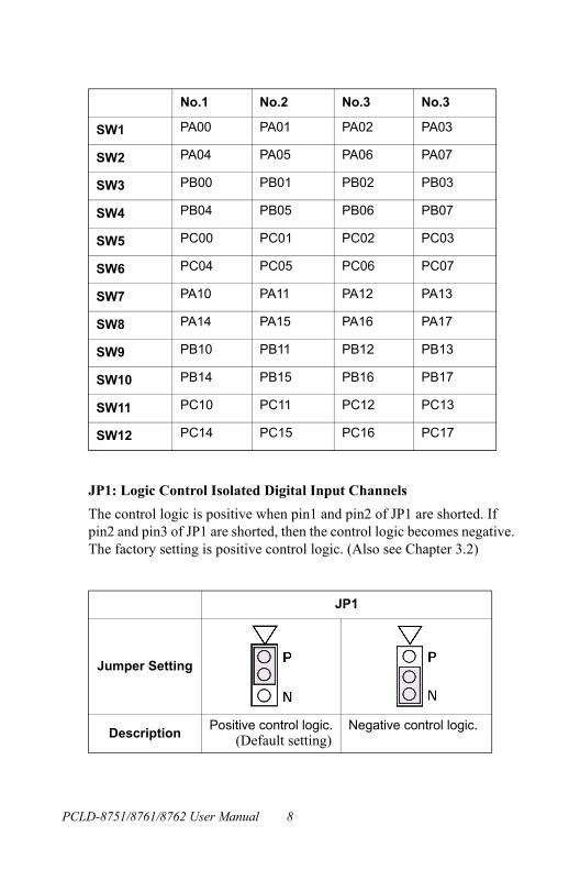
JP1: Logic Control Isolated Digital Input Channels
The control logic is positive when pin1 and pin2 of JP1 are shorted. If pin2 and pin3 of JP1 are shorted, then the control logic becomes negative. The factory setting is positive control logic. (Also see Chapter 3.2)
No.1 No.2 No.3 No.3
SW1 PA00 PA01 PA02 PA03
SW2 PA04 PA05 PA06 PA07
SW3 PB00 PB01 PB02 PB03
SW4 PB04 PB05 PB06 PB07
SW5 PC00 PC01 PC02 PC03
SW6 PC04 PC05 PC06 PC07
SW7 PA10 PA11 PA12 PA13
SW8 PA14 PA15 PA16 PA17
SW9 PB10 PB11 PB12 PB13
SW10 PB14 PB15 PB16 PB17
SW11 PC10 PC11 PC12 PC13
SW12 PC14 PC15 PC16 PC17
JP1
Jumper Setting
DescriptionPositive control logic.
(Default setting)Negative control logic.
PCLD-8751/8761/8762 User Manual 8

2.2.2 PCLD-8761 (24-Ch Isolated DI and 24-Ch Relay Output Board)
9 Chapter 2

CN1: SCSI 68-pin Connector
PCLD-8751/8761/8762 User Manual 10

TB1/TB2/TB3/TB4: Wiring Terminal Block
TB5: External Connector for Dry Contact Isolated DI Channels
External power source connector for Dry contact mode isolation input channels. When using Dry contact input mode, it is necessary to provide external power through TB5. The voltage range is +5V ~ 30V DC.
TB6: Reserved for the Counter Function on PCI-1751/PCI-1751U
TB7: External Power Source Connector
PCLD-8761’s driving power can be set as external by JP3, and the input voltage range is DC +7 ~ +30V.
TB1 TB2 TB3 TB4
Name Pin Name Pin Name Pin Name Pin
PA00 1+,1- PB04 13+,13-
PA10 25COM,25NC,25NO
PB14 37COM,37NC,37NO
PA01 2+,2- PB05 14+,14-
PA11 26COM,26NC,26NO
PB15 38COM,38NC,38NO
PA02 3+,3- PB06 15+,15-
PA12 27COM,27NC,27NO
PB16 39COM,39NC,39NO
PA03 4+,4- PB07 16+,16-
PA13 28COM,28NC,28NO
PB17 40COM,40NC,40NO
PA04 5+,5- PC00 17+,17-
PA14 29COM,29NC,29NO
PC10 41COM,41NC,41NO
PA05 6+,6- PC01 18+,18-
PA15 30COM,30NC,30NO
PC11 42COM,42NC,42NO
PA06 7+,7- PC02 19+,19-
PA16 31COM,31NC,31NO
PC12 43COM,43NC,43NO
PA07 8+,8- PC03 20+,20-
PA17 32COM,32NC,32NO
PC13 44COM,44NC,44NO
PB00 9+,9- PC04 21+,21-
PB10 33COM,33NC,33NO
PC14 45COM,45NC,45NO
PB01 10+,10-
PC05 22+,22-
PB11 34COM,34NC,34NO
PC15 46COM,46NC,46NO
PB02 11+,11-
PC06 23+,23-
PB12 35COM,35NC,35NO
PC16 47COM,47NC,47NO
PB03 12+,12-
PC07 24+,24-
PB13 36COM,36NC,36NO
PC17 48COM,48NC,48NO
11 Chapter 2

SW1~SW6: Wet/Dry Contact Selection
SW1 ~ SW12 are used to switch the input channels as “Wet Contact” or “Dry Contact”. The factory settings of the switches are in “Off” position, and the input channels are in Wet contact mode.
You can set each input channel as Dry contact mode by setting the switch to the “On” position. Following is the mapping table of the DIP switch and the input channels.
JP1/JP2: Logic Control for Isolated Input & Relay Output Channels
The control logic of isolated digital input and relay output channels can be set separately. The control logic is positive when pin1 and pin2 are shorted. If pin2 and pin3 are shorted, then the control logic becomes neg-ative. The factory setting is positive control logic. (Also see Chapter 3.2)
No.1 No.2 No.3 No.3
SW1 PA00 PA01 PA02 PA03
SW2 PA04 PA05 PA06 PA07
SW3 PB00 PB01 PB02 PB03
SW4 PB04 PB05 PB06 PB07
SW5 PC00 PC01 PC02 PC03
SW6 PC04 PC05 PC06 PC07
JP1 (Isolated DI)/ JP2 (Relay Output)
Jumper Setting
)
DescriptionPositive control logic.
(Default setting)Negative control logic.
PCLD-8751/8761/8762 User Manual 12
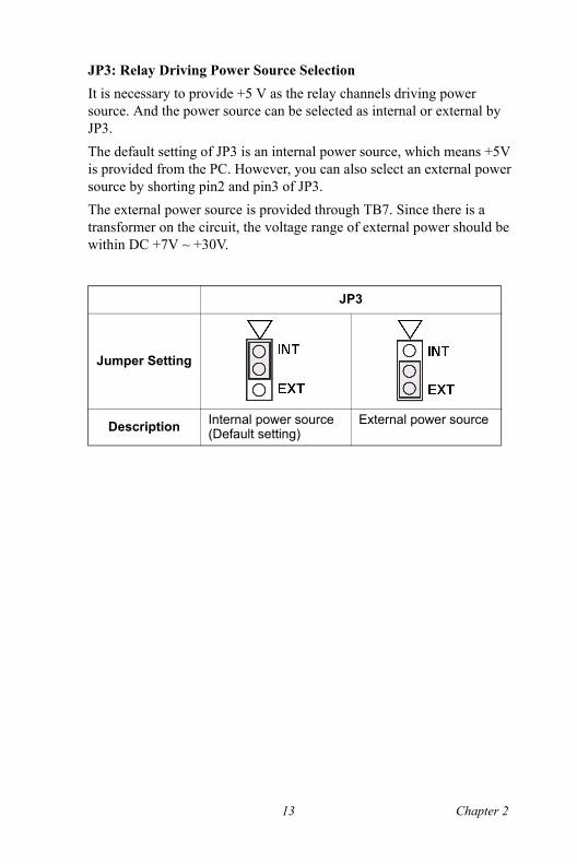
JP3: Relay Driving Power Source Selection
It is necessary to provide +5 V as the relay channels driving power source. And the power source can be selected as internal or external by JP3.
The default setting of JP3 is an internal power source, which means +5V is provided from the PC. However, you can also select an external power source by shorting pin2 and pin3 of JP3.
The external power source is provided through TB7. Since there is a transformer on the circuit, the voltage range of external power should be within DC +7V ~ +30V.
JP3
Jumper Setting
Description Internal power source (Default setting)
External power source
13 Chapter 2

2.2.3 PCLD-8762 (48-Channel Relay Output Board)
PCLD-8751/8761/8762 User Manual 14

CN1: SCSI 68-pin Connector
15 Chapter 2

,37O,38O,39O,40O,41O,42O,43O,44O,45O,46O,47O,48O
TB1/TB2/TB3/TB4: Wiring Terminal Block
TB5: External Power Source Connector
PCLD-8762 requires an external driving power source and the voltage range of the power source should be within DC +7V ~ +30V.
JP1: Logic Control for Relay Output Channels
The control logic is positive when pin1 and pin2 of JP1 are shorted. If pin2 and pin3 of JP1 are shorted, then the control logic becomes negative. The factory setting is positive control logic. (Also see Chapter 3.2)
TB1 TB2 TB3 TB4
Name Pin Name Pin Name Pin Name Pin
PA00 1COM,1NC,1NO
PB04 13COM,13NC,13NO
PA10 25COM,25NC,25NO
PB14 37COMNC,37N
PA01 2COM,2NC,2NO
PB05 14COM,14NC,14NO
PA11 26COM,26NC,26NO
PB15 38COMNC,38N
PA02 3COM,3NC,3NO
PB06 15COM,15NC,52NO
PA12 27COM,27NC,27NO
PB16 39COMNC,39N
PA03 4COM,4NC,4NO
PB07 16COM,16NC,16NO
PA13 28COM,28NC,28NO
PB17 40COMNC,40N
PA04 5COM,5NC,5NO
PC00 17COM,17NC,17NO
PA14 29COM,29NC,29NO
PC10 41COMNC,41N
PA05 6COM,6NC,6NO
PC01 18COM,18NC,18NO
PA15 30COM,30NC,30NO
PC11 42COMNC,42N
PA06 7COM,7NC,7NO
PC02 19COM,19NC,19NO
PA16 31COM,31NC,31NO
PC12 43COMNC,43N
PA07 8COM,8NC,8NO
PC03 20COM,20NC,20NO
PA17 32COM,32NC,32NO
PC13 44COMNC,44N
PB00 9COM,9NC,9NO
PC04 21COM,21NC,21NO
PB10 33COM,33NC,33NO
PC14 45COMNC,45N
PB01 10COM,10NC,10NO
PC05 22COM,22NC,22NO
PB11 34COM,34NC,34NO
PC15 46COMNC,46N
PB02 11COM,11NC,11NO
PC06 23COM,23NC23NO
PB12 35COM,35NC,35NO
PC16 47COMNC,47N
PB03 12COM,12NC,12NO
PC07 24COM,24NC,24NO
PB13 36COM,36NC,36NO
PC17 48COMNC,48N
JP1
Jumper Setting
DescriptionPositive control logic.
(Default setting)Negative control logic.
PCLD-8751/8761/8762 User Manual 16
2
CH
AP
TE
R
3
Operations
This chapter has information for oper-ating PCLD-8751, PCLD-8761 & PCLD-8762.
Sections include:
• Power Source Selection
• Control Logic
• Wiring

Chapter 3 Operations
3.1 Power Source Selection
PCLD-8751, PCLD-8761, and PCLD-8762 require a +5V power supply for correct operation. When using the SCSI 68-pin connector, PCLD-8751 and PCLD-8761 can be powered directly from the PCI bus by con-necting CN1 to any Advantech PC-LabCard product. It is also possible to connect external supplies to PCLD-8761 by connecting an external power supply to terminal TB7. It is recommended to use an external power source when more than 8 relay channels are operated. Correct connec-tions are shown in section 2.2. However, the external power supply is required for PCLD-8762 in any circumstance to ensure normal functions.
3.2 Control Logic
The preferred control logic can be defined by setting the on-board jumper JP1 (PCLD-8751, PCLD-8761, and PCLD-8762) and JP2 (PCLD-8761). The default setting the positive logic, which means logic "1" = device activated. For input channels, when the inputs are activated, the DI chan-nels will be TTL “1”. And for DO channels, the relay will operate for a TTL high (+5V) on the input (common contact connected to NO contact). The relay will release for a TTL low on the input (common contact con-nected to NC contact).
On the other hand, when the jumper was set as negative logic, which means logic "0" = device activated. For input channels, the relay will operate for a TTL low (0V) on the input (common contact connected to NO contact). The relay will release for a TTL high on the input (common contact connected to NC contact).
PCLD-8751/8761/8762 User Manual 18

3.3 Wiring
3.3.1 Isolated DI
Wet Contact Dry Contact
VC
C
IDI
2K
D52
1N41
48
InL
InH
PC
357
1 2
4 3
1K TVS
1 2
EX
Pow
er+
1K
TB
5TB
CK
2
1 2
VC
CIn
H
IDI
2K
TV
S
1 2
EX
Pow
er-
PC
357
1 2
4 3
InL
D52
1N
4001
19 Chapter 3

Relay
DO
470
LED
DO
_CO
MD
O_N
C
RE
LAY
910 8
43 5
1 12
DO
_NO
VC
C
VC
C
PCLD-8751/8761/8762 User Manual 20

2
AP
PE
ND
IX
A
Specifications

Appendix A Specifications
A.1 Isolated Digital Input
A.2 Relay Output
ChannelsPCLD-8751 48PCLD-8761 24
Isolation Voltage 2500 VDC
Input Range(Wet Contact)
VIH(max.) 30VVIH(min.) 4VVIL(max.) 1V
Input Range(Dry Contact)
External Power DV +5~30VVIH ShoutVIL Open
Number of Output Channel PCLD-8761 24PCLD-8762 48
Relay Type Form C (SPDT)
Contact Rating (resistive) 0.25A@250VAC, 2A@30VDC
Max. Switching Power 62.5VA, 60W
Max. Switching Voltage 250VAC, 220VDC
Max. Switching Current 5A
Min. Switching Voltage 100μV
Breakdown Voltage
Between Coil and Contacts
1500VAC min. (1 minute)
Between Open Contacts
1000VAC min. (1 minute)
Between Adjacent Contacts
1000VAC min. (1 minute)
Operate/Release Time typ. 3 / 2 ms, max. 5 / 4 ms
Resistance Contact: 50 mΩ max. @ 10mA/20mVInsulation: 1 GΩ min. @ 500VDC
Life Expectancy
Mechanical 108 cycles typ.
Electrical 5 x 10⁷ cycles typ. @ 10mA/12V
2 x 10⁵ cycles typ. @ 2000mA/30V
PCLD-8751/8761/8762 User Manual 22

A.3 General
Dimensions PCLD-8751 255 x 121mmPCLD-8761 285 x 121mmPCLD-8762 285 x 121mm
Power Consumption
PCLD-8751 Max. +5 V @ < 0.6 APCLD-8761 Max. +5 V @ < 1.6 APCLD-8762 Max.+7V @ 1.8A
+30V @ 0.45A
Screw Terminal Accepts #14 to #24 AWG wires
23 Appendix A

PCLD-8751/8761/8762 User Manual 24