42s16400(E..) - insideGadgets
68
IC42S16400 Integrated Circuit Solution Inc. 1 DR034-0E 12/02/2003 Document Title 1M x 16Bit x 4 Banks (64-MBIT) SDRAM Revision History Revision No History Draft Date Remark 0A Initial Draft Demcember 20,2001 0B Revise DC OPERATING CONDITIONS April 15,2002 0C 1. add -6ns speed grade Novembver 22,2002 2. obsolete 8Mx8 configuration 3. obsolete Low power version 4. obsolete -8ns speed grade 0D Add 60 ball(64M SDRAM) VF-BGA package September 05,2003 0E Add Pb-free package December 02,2003 The attached datasheets are provided by ICSI. Integrated Circuit Solution Inc reserve the right to change the specifications and products. ICSI will answer to your questions about device. If you have any questions, please contact the ICSI offices.
Transcript of 42s16400(E..) - insideGadgets

IC42S16400
Integrated Circuit Solution Inc. 1DR034-0E 12/02/2003
Document Title1M x 16Bit x 4 Banks (64-MBIT) SDRAM
Revision HistoryRevision No History Draft Date Remark0A Initial Draft Demcember 20,20010B Revise DC OPERATING CONDITIONS April 15,20020C 1.add -6ns speed grade Novembver 22,2002
2.obsolete 8Mx8 configuration3.obsolete Low power version4.obsolete -8ns speed grade
0D Add 60 ball(64M SDRAM) VF-BGA package September 05,20030E Add Pb-free package December 02,2003
The attached datasheets are provided by ICSI. Integrated Circuit Solution Inc reserve the right to change the specifications andproducts. ICSI will answer to your questions about device. If you have any questions, please contact the ICSI offices.
IC42S16400
2 Integrated Circuit Solution Inc.DR034-0E 12/02/2003
ICSI reserves the right to make changes to its products at any time without notice in order to improve design and supply the best possible product. We assume no responsibility for any errorswhich may appear in this publication. © Copyright 2000, Integrated Circuit Solution Inc.
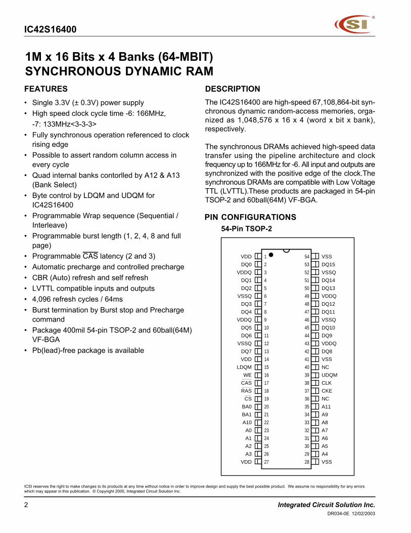
FEATURES• Single 3.3V (± 0.3V) power supply• High speed clock cycle time -6: 166MHz,
-7: 133MHz<3-3-3>• Fully synchronous operation referenced to clock
rising edge• Possible to assert random column access in
every cycle• Quad internal banks contorlled by A12 & A13
(Bank Select)• Byte control by LDQM and UDQM for
IC42S16400• Programmable Wrap sequence (Sequential /
Interleave)• Programmable burst length (1, 2, 4, 8 and full
page)• Programmable CAS latency (2 and 3)• Automatic precharge and controlled precharge• CBR (Auto) refresh and self refresh• LVTTL compatible inputs and outputs• 4,096 refresh cycles / 64ms• Burst termination by Burst stop and Precharge
command• Package 400mil 54-pin TSOP-2 and 60ball(64M)
VF-BGA• Pb(lead)-free package is available
DESCRIPTIONThe IC42S16400 are high-speed 67,108,864-bit syn-chronous dynamic random-access memories, orga-nized as 1,048,576 x 16 x 4 (word x bit x bank),respectively.
The synchronous DRAMs achieved high-speed datatransfer using the pipeline architecture and clockfrequency up to 166MHz for -6. All input and outputs aresynchronized with the positive edge of the clock.Thesynchronous DRAMs are compatible with Low VoltageTTL (LVTTL).These products are packaged in 54-pinTSOP-2 and 60ball(64M) VF-BGA.
1M x 16 Bits x 4 Banks (64-MBIT)SYNCHRONOUS DYNAMIC RAM
1
2
3
4
5
6
7
8
9
10
11
12
13
14
15
16
17
18
19
20
21
22
23
24
25
26
27
54
53
52
51
50
49
48
47
46
45
44
43
42
41
40
39
38
37
36
35
34
33
32
31
30
29
28
VDD
DQ0
VDDQ
DQ1
DQ2
VSSQ
DQ3
DQ4
VDDQ
DQ5
DQ6
VSSQ
DQ7
VDD
LDQM
WE
CAS
RAS
CS
BA0
BA1
A10
A0
A1
A2
A3
VDD
VSS
DQ15
VSSQ
DQ14
DQ13
VDDQ
DQ12
DQ11
VSSQ
DQ10
DQ9
VDDQ
DQ8
VSS
NC
UDQM
CLK
CKE
NC
A11
A9
A8
A7
A6
A5
A4
VSS
PIN CONFIGURATIONS54-Pin TSOP-2
IC42S16400
Integrated Circuit Solution Inc. 3DR034-0E 12/02/2003
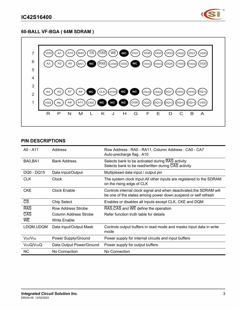
60-BALL VF-BGA ( 64M SDRAM )
R P N M L K J H G F E D C B A
VSS
A4
A6
A5
A8
A7
A11
A9
CKE
NC
NC
CLK
NC
UDQM
NC
NC
A3
VDD
A2
A1
A0
A10
BA1
BA0
NC
CS
RAS
CAS
LDQM
WE NC
DQ8
NC
DQ9
VDDQ
DQ10
VSSQ
DQ12
DQ11
DQ13
VDDQ
NC
DQ7
VSSQ
DQ6
VDDQ
DQ5
DQ4
DQ3
VSSQ
DQ2
DQ14
VSSQ
VSS
DQ15
VDDQ
DQ1
DQ0
VDD7
6
5
4
3
2
1
VDD
PIN DESCRIPTIONS
A0 - A11 Address Row Address : RA0 - RA11, Column Address : CA0 - CA7Auto-precharge flag : A10
BA0,BA1 Bank Address Selects bank to be activated during RAS activitySelects bank to be read/written during CAS activity
DQ0 - DQ15 Data Input/Output Multiplexed data input / output pinCLK Clock The system clock input.All other inputs are registered to the SDRAM
on the rising edge of CLK
CKE Clock Enable Controls internal clock signal and when deactivated,the SDRAM willbe one of the states among power down,suspend or self refresh
CS Chip Select Enables or disables all inputs except CLK, CKE and DQMRAS Row Address Strobe RAS,CAS and WE define the operationCAS Column Address Strobe Refer function truth table for detailsWE Write Enable
LDQM,UDQM Data Input/Output Mask Controls output buffers in read mode and masks input data in writemode
VDD/VSS Power Supply/Ground Power supply for internal circuits and input buffersVDDQ/VSSQ Data Output Power/Ground Power supply for output buffers
NC No Connection No Connection

IC42S16400
4 Integrated Circuit Solution Inc.DR034-0E 12/02/2003
FUNCTIONAL BLOCK DIAGRAM
CLK
CKE
ClockGenerator
CS
RAS
ModeRegister
ColumnAddressBuffer
&BurstCounter
CAS
WE
Com
man
d D
ecod
er
Con
trol
Lo
gic
Address RowAddressBuffer
&RefreshCounter
Bank B
Bank A
Sense Amplifier
Column Decoder &Latch Circuit
Row
Dec
oder
Data Control Circuit DQ
DQM
Latc
h C
ircui
t
Inpu
t & O
utpu
tB
uffe
r
Bank CBank D

IC42S16400
Integrated Circuit Solution Inc. 5DR034-0E 12/02/2003
ABSOLUTE MAXIMUM RATINGS(1)
Symbol Parameters Rating UnitVDD Supply Voltage (with respect to VSS) –0.5 to +4.6 VVDDQ Supply Voltage for Output (with respect to VSSQ) –0.5 to +4.6 VVI Input Voltage (with respect to VSS) –0.5 to VDD+0.5 VVO Output Voltage (with respect to VSSQ) –1.0 to VDDQ+0.5 VIO Short circuit output current 50 mAPD Power Dissipation (TA = 25 °C) 1 WTOPT Operating Temperature 0 to +70 °CTSTG Storage Temperature –65 to +150 °CNotes:1. Exposing the device to stress above those listed in Absolute Maximum Ratings could cause permanent
damage. The device is not meant to be operated under conditions outside the limits described in theoperational section of this specification. Exposure to Absolute Maximum Rating conditions for extendedperiods may affect device reliability.
DC RECOMMENDED OPERATING CONDITIONS(At TA = 0 to +70°C unless otherwise noted)
Symbol Parameter Min. Typ. Max. UnitVDD Supply Voltage 3.0 3.3 3.6 VVDDQ Supply Voltage for DQ 3.0 3.3 3.6 VVIH High Level Input Voltage (all Inputs) 2.0 — VDD + 0.3 VVIL Low Level Input Voltage (all Inputs) -0.3 — +0.8 V
CAPACITANCE CHARACTERISTICS(At TA = 0 ~ 70°C, VDD = VDDQ = 3.3 ± 0.3V, VSS = VSSQ = 0V , unless otherwise noted)
Symbol Parameter Min. Max. UnitCIN Input Capacitance, address & control pin 2.5 3.8 pFCCLK Input Capacitance, CLK pin 2.5 3.5 pFCI/O Data Input/Output Capacitance 4.0 6.5 pF

IC42S16400
6 Integrated Circuit Solution Inc.DR034-0E 12/02/2003
DC ELECTRICAL CHARACTERISTICS (At TA = 0 ~ 70°C, VDD = VDDQ = 3.3 ± 0.3V, VSS = VSSQ = 0V , unless otherwise noted)
Symbol Parameter Test Condition Speed Min. Max. UnitICC1(1) Operating Current One Bank active, CAS latency = 3 -6(42S16400) — 95 mA
Burst Length=1 -7(42S16400) — 85 mAtRC = tRC (min.)tCLK = tCLK (min.)
ICC2P Precharge Standby Current CKE < VIL (MAX) tCK = 15 ns -6 — 2 mA(In Power-Down Mode) -7 — 2 mA
ICC2PS CKE < VIL (MAX) CLK < VIL (MAX) -6 — 1 mA-7 — 1 mA
ICC2N(2) Precharge Standby Current CS > VCC -0.2V tCK = 15 ns -6 — 20 mA(In Non Power-Down Mode) CKE > VIH (MIN) -7 — 20 mA
ICC2NS CS > VCC -0.2V CKE < VIL (MAX) -6 — 15 mACKE > VIH (MIN) All input signals are stable. -7 — 15 mA
ICC3P Active Standby Current CKE < VIL (MAX) tCK = 10 ns -6 — 7 mA(In Power-Down Mode) -7 — 7 mA
ICC3PS CKE < VIL (MAX) CLK < VIL (MAX) -6 — 5 mA-7 — 5 mA
ICC3N(2) Active Standby Current CS > VCC -0.2V tCK = 15 ns -6 — 30 mA(In Non Power-Down Mode) CKE > VIH (MIN) -7 — 30 mA
ICC3NS CS > VCC -0.2V CKE < VIL (MAX) -6 — 25 mACKE > VIH (MIN) All input signals are stable. -7 — 25 mA
ICC4 Operating Current All Banks active CAS latency = 3 -6(42S16400) — 130 mA(In Burst Mode) Burst Length=1 -7(42S16400) — 100 mA
tCK = tCK (MIN)ICC5 Auto-Refresh Current tRC = tRC (MIN) -6 — 150 mA
tCLK = tCLK (MIN) -7 — 130 mAICC6(3, 4) Self-Refresh Current CKE < 0.2V -6 — 1 mA
-7 — 1 mAIIL Input Leakage Current 0V < VIN < VDD (MAX) –5 5 µA
(Inputs) Pins not under test = 0VIOL Output Leakage Current Output is disabled DQ# in H - Z., –5 5 µA
(I/O pins) 0V < VOUT < VDD (MAX)VOH High Level Output Voltage IOUT = –2 mA 2.4 — VVOL Low Level Output Voltage IOUT = +2 mA — 0.4 V
Notes:1. ICC(max) is specified at the output open condition.2. Input signals are changed one time during 30ns.

IC42S16400
Integrated Circuit Solution Inc. 7DR034-0E 12/02/2003
AC TEST CONDITIONS(At TA = 0 ~ 70°C, VDD = VDDQ = 3.3 ± 0.3V, VSS = VSSQ = 0V , unless otherwise noted)
Parameter Rating UnitAC input Levels (VIH /VIL ) 2.0 / 0.8 VInput timing reference level /Output timing reference level 1.4 VInput rise and fall time 1 ns
Output load condition 50 pF
Ω
VDDQ VDDQ
VOUT
DeviceUnderTest
50PF
Z = 50
Output Load Conditions

IC42S16400
8 Integrated Circuit Solution Inc.DR034-0E 12/02/2003
AC ELECTRICAL CHARACTERISTICS (At TA = 0 ~ 70°C, VDD = VDDQ = 3.3 ± 0.3V, VSS = VSSQ = 0V , unless otherwise noted)
-6 -7Symbol Parameter Min. Max. Min. Max. UnitstCK3 CLK Cycle Time CAS Latency = 3 6 — 7.5 — nstCK2 CAS Latency = 2 7.5 — 10 — nstAC3 CLK to valid output delay(1) CAS Latency = 3 — 5 — 5.4 nstAC2 CAS Latency = 2 — 6 — 6 nstCH CLK high pulse width 2.5 — 2.5 — nstCL CLK low pulse width 2.5 — 2.5 — nstCKE CKE setup time 1.5 — 1.5 — nstCKH CKE hold time 0.8 — 0.8 — nstAS Address setup time 1.5 — 1.5 — nstAH Address hold time 0.8 — 0.8 — nstCMS Command setup time 1.5 — 1.5 — nstCMH Command hold time 0.8 — 0.8 — nstDS Data input setup time 1.5 — 1.5 — nstDH Data input hold time 0.8 — 0.8 — nstOH3 Output data hold time(1) CAS Latency = 3 2.5 — 2.7 — nstOH2 CAS Latency = 2 2.5 — 3 — nstLZ CLK to output in low - Z 0 — 0 — nstHZ CLK to output in H - Z 2.5 5 2.7 5.4 nstRC ROW cycle time 60 — 67.5 — nstRAS ROW active time 42 100,000 45 100,000 nstRCD RAS to CAS delay 18 — 20 — nstRP Row precharge time 15 — 20 — nstRRD Row active to active delay 12 — 15 — nstDPL Data in to precharge 12 — 15 — nstT Transition time 1 10 1 10 nstRSC Mode reg. set cycle 10 — 10 — nstPDE Power down exit setup time 7.5 — 7.5 — nstSRX Self refresh exit time 7.5 — 7.5 — nstREF Refresh Time — 64 — 64 ms
Notes:1. if clock rising time is longer than 1ns, (tr/2-0.5ns) should be added to the parameter.

IC42S16400
Integrated Circuit Solution Inc. 9DR034-0E 12/02/2003
Basic Features and Function Description
Simplified State Diagram
SelfRefresh
MRSModeRegister
SetIDLE
AUTORefresh
REF
AC
T
CKE
CKE
BST
PowerDown
ActivePowerDown
ROWACTIVE
Read
CKE
CKE
READ READSUSPEND
CKE
CKEREAD AREADA
SUSPEND
Read withAuto Precharge
CKE
CKE
Write (Write recovery)
WRITEWRITESUSPEND
WRITE AWRITE ASUSPEND
CKE
CKE
Write withAuto Precharge
POWERON
Precharge Precharge
PR
E (Precharge term
ination)
PRE
(Pre
char
ge te
rmin
atio
n)
Read w
ithWrit
e w
ithAu
to p
rech
arge
Auto Precharge
Read
BST
Write
Read with
Auto Precharge (write recovery)
Write with
Auto PrechargeWrite
Read (write recovery)
PR
E
CKECKE
Automatic sequenceManual input
Note: After the AUTO refresh operation, precharge operation isperformed automatically and enter the IDLE state
SELF entr
y
SELF exit
Writ
e re
cove
ry

IC42S16400
10 Integrated Circuit Solution Inc.DR034-0E 12/02/2003
COMMAND TRUTH TABLE
CKE A11Symbol Command n-1 n CSCSCSCSCS RASRASRASRASRAS CASCASCASCASCAS WEWEWEWEWE BA A10 A9-A0DESL Device deselect H X H X X X X X XNOP No operation H X L H H H X X XMRS Mode register set H X L L L L L L VACT Bank activate H X L L H H V V VREAD Read H X L H L H V L VREADA Read with auto precharge H X L H L H V H VWRIT Write H X L H L L V L VWRITA Write with auto precharge H X L H L L V H VPRE Precharge select bank H X L L H L V L XPALL Precharge all banks H X L L H L X H XBST Burst stop H X L H H L X X XREF CBR (Auto) refresh H H L L L H X X XSELF Self refresh H L L L L H X X X
Notes:H : High level L : Low levelX : High or Low level (Don’t care) V : Valid Data input
DQM TRUTH TABLE
CKESymbol Command n-1 n DQMENB Data Write / Output Enable H X LMASK Data Mask / Output Disable H X H
CKE TRUTH TABLE
CKESymbol Command Current State n-1 n CSCSCSCSCS RASRASRASRASRAS CASCASCASCASCAS WEWEWEWEWE Addreess— Clock suspend mode entry Activating H L X X X X X— Clock suspend Any L L X X X X X— Clock suspend mode exit Clock suspend L H X X X X XREF CBR refresh command Idle H H L L L H XSELF Self refresh entry Idle H L L L L H X— Self refresh exit Self refresh L H L H H H X
L H H X X X X— Power down entry Idle H L X X X X X— Power down exit Power down L H X X X X X

IC42S16400
Integrated Circuit Solution Inc. 11DR034-0E 12/02/2003
OPERATION COMMAND TABLE(1)
Current State Command Operation CSCSCSCSCS RASRASRASRASRAS CASCASCASCASCAS WEWEWEWEWE AddressIdle DESL NOP or Power-Down(2) H X X X X
NOP or BST NOP or Power-Down(2) L H H X XREAD / READA Illegal(3) L H L H BA, CA, A10WRIT/WRITA Illegal(3) L H L L BA, CA, A10ACT Row Active L L H H BR, RAPRE/PALL NOP L L H L BA, A10REF/SELF Refresh or Self-Refresh(4) L L L H XMRS Mode Register Set L L L L Op-Code
Row Active DESL NOP H X X X XNOP or BST NOP L H H H XREAD/READA Begin read : Determine AP(5) L H L H BA, CA, A10WRIT/WRITA Begin write : Determine AP(5) L H L L BA, CA, A10ACT Illegal(3) L L H H BR, RAPRE/PALL Precharge(6) L L H L BA, A10REF/SELF Illegal L L L H XMRS Illegal L L L L Op-Code
Read DESL Continue burst to end -> Row active H X X X XNOP Continue burst to end -> Row active L H H H XBST Burst stop -> Row active L H H L XREAD/READA Term burst, new read : Determine AP(7) L H L H BA, CA, A10WRIT/WRITA Term burst, start write : Determine AP(7, 8) L H L L BA, CA, A10ACT Illegal(3) L L H H BR, RAPRE/PALL Term burst, precharging L L H L BA, A10REF/SELF Illegal L L L H XMRS Illegal L L L L Op-Code
Write DESL Continue burst to end -> write recovering H X X X XNOP Continue burst to end -> write recovering L H H H XBST Burst stop -> Row active L H H L XREAD/READA Term burst, start read : Determine AP(7, 8) L H L H BA, CA, A10WRIT/WRITA Term burst, new write : Determine AP(7) L H L L BA, CA, A10ACT Illegal(3) L L H H BR, RAPRE/PALL Term burst, precharging(9) L L H L BA, A10REF/SELF Illegal L L L H XMRS Illegal L L L L Op-Code
Read With DESL Continue burst to end -> Precharging H X X X XAuto- NOP Continue burst to end -> Precharging L H H H XPrecharge BST Illegal L H H L X
READ/READA Illegal(11) L H L H BA, CA, A10WRIT/WRITA Illegal(11) L H L L BA, CA, A10ACT Illegal(3) L L H H BR, RAPRE/PALL Illegal(11) L L H L BA, A10REF/SELF Illegal L L L H XMRS Illegal L L L L Op-Code

IC42S16400
12 Integrated Circuit Solution Inc.DR034-0E 12/02/2003
OPERATION COMMAND TABLE(continue)
Current State Command Operation CSCSCSCSCS RASRASRASRASRAS CASCASCASCASCAS WEWEWEWEWE AddressWrite with auto DESL Continue burst to end -> write recovering with auto precharge H X X X Xprecharge NOP Continue burst to end -> write recovering with auto precharge L H H H X
BST Illegal L H H L XREAD / READA Illegal(11) L H L H BA, CA, A10WRIT/WRITA Illegal(11) L H L L BA, CA, A10ACT Illegal(3, 11) L L H H BR, RAPRE/PALL Illegal(3, 11) L L H L BA, A10REF/SELF Illegal L L L H XMRS Illegal L L L L Op-Code
Precharging DESL Nop -> Enter idle after tRP H X X X XNOP Nop -> Enter idle after tRP L H H H XBST Nop -> Enter idle after tRP L H H L XREAD/READA Illegal(3) L H L H BA, CA, A10WRIT/WRITA Illegal(3) L H L L BA, CA, A10ACT Illegal(3) L L H H BR, RAPRE/PALL Nop -> Enter idle after tRP L L H L BA, A10REF/SELF Illegal L L L H XMRS Illegal L L L L Op-Code
Row activating DESL Nop - > Enter row active after tRCD H X X X XNOP Nop - > Enter row active after tRCD L H H H XBST Nop - > Enter row active after tRCD L H H L XREAD/READA Illegal(3) L H L H BA, CA, A10WRIT/WRITA Illegal(3) L H L L BA, CA, A10ACT Illegal(3, 9) L L H H BR, RAPRE/PALL Illegal(3) L L H L BA, A10REF/SELF Illegal L L L H XMRS Illegal L L L L Op-Code
Write DESL Nop -> Enter row active after tDPL H X X X Xrecovering NOP Nop -> Enter row active after tDPL L H H H X
BST Nop -> Enter row active after tDPL L H H L XREAD/READA Start read, Determine AP(8) L H L H BA, CA, A10WRIT/WRITA New write, Determine AP L H L L BA, CA, A10ACT Illegal(3) L L H H BR, RAPRE/PALL Illegal(3) L L H L BA, A10REF/SELF Illegal L L L H XMRS Illegal L L L L Op-Code

IC42S16400
Integrated Circuit Solution Inc. 13DR034-0E 12/02/2003
OPERATION COMMAND TABLE(continue)
Current State Command Operation CSCSCSCSCS RASRASRASRASRAS CASCASCASCASCAS WEWEWEWEWE AddressWrite DESL Nop -> Enter precharge after tDPL H X X X Xrecovering NOP Nop -> Enter precharge after tDPL L H H H Xwith auto BST Nop -> Enter precharge after tDPL L H H L Xprecharge READ/READA Illegal(3 ,8, 11) L H L H BA, CA, A10
WRIT/WRITA Illegal(3,11) L H L L BA, CA, A10ACT Illegal(3, 11) L L H H BR, RAPRE/PALL Illegal(3, 11) L L H L BA, A10REF/SELF Illegal L L L H XMRS Illegal L L L L Op-Code
Auto DESL Nop Enter idle after tRC H X X X XRefreshing NOP/BST Nop Enter idle after tRC L H H X X
READ/WRIT Illegal L H L X XACT/PRE/PALL Illegal L L H X XREF/SELF/MRS Illegal L L L X X
Mode DESL Nop -> Enter idle after 2 Clocks H X X X Xregister NOP Nop -> Enter idle after 2 Clocks L H H H Xsetting BST Illegal L H H L X
READ/WRIT Illegal L H L X XACT/PRE/PALL/ Illegal L L X X XREF/SELF/MRS
Notes:1. All entries assume that CKE was active (High level) during the preceding clock cycle.2. If both banks are idle, and CKE is inactive (Low level), the device will enter Power downmode. All input buffers except CKE
will be disabled.3. Illegal to bank in specified states; Function may be legal in the bank indicated by Bank Address(BA), depending on the
state of that bank.4. If both banks are idle, and CKE is inactive (Low level), the device will enter Self refresh mode. All input buffers except CKE
will be disabled.5. Illegal if tRCD is not satisfied.6. Illegal if tRAS is not satisfied.7. Must satisfy burst interrupt condition.8. Must satisfy bus contention, bus turn around, and/or write recovery requirements.9. Must mask preceding data which don’t satisfy tDPL .10. Illegal if tRRD is not satisfied.11. Illegal for single bank, but legal for other banks in multi-bank devices.

IC42S16400
14 Integrated Circuit Solution Inc.DR034-0E 12/02/2003
CKE RELATED COMMAND TRUTH TABLE(1)
CKECurrent State Operation n-1 n CSCSCSCSCS RASRASRASRASRAS CASCASCASCASCAS WEWEWEWEWE AddressSelf-Refresh (S.R.) INVALID, CLK (n - 1)would exit S.R. H X X X X X X
Self-Refresh Recovery(2) L H H X X X XSelf-Refresh Recovery(2) L H L H H X XIllegal L H L H L X XIllegal L H L L X X XMaintain S.R. L L X X X X X
Self-Refresh Recovery Idle After tRC H H H X X X XIdle After tRC H H L H H X XIllegal H H L H L X XIllegal H H L L X X XBegin clock suspend next cycle(5) H L H X X X XBegin clock suspend next cycle(5) H L L H H X XIllegal H L L H L X XIllegal H L L L X X XExit clock suspend next cycle(2) L H X X X X XMaintain clock suspend L L X X X X X
Power-Down (P.D.) INVALID, CLK (n - 1) would exit P.D. H X X X X X —EXIT P.D. -> Idle(2) L H X X X X XMaintain power down mode L L X X X X X
Both Banks Idle Refer to operations in Operative Command Table H H H X X X —Refer to operations in Operative Command Table H H L H X X —Refer to operations in Operative Command Table H H L L H X —Auto-Refresh H H L L L H XRefer to operations in Operative Command Table H H L L L L Op - CodeRefer to operations in Operative Command Table H L H X X X —Refer to operations in Operative Command Table H L L H X X —Refer to operations in Operative Command Table H L L L H X —Self-Refresh(3) H L L L L H XRefer to operations in Operative Command Table H L L L L L Op - CodePower-Down(3) L X X X X X X
Any state Refer to operations in Operative Command Table H H X X X X Xother than Begin clock suspend next cycle(4) H L X X X X Xlisted above Exit clock suspend next cycle L H X X X X X
Maintain clock suspend L L X X X X XNotes:1. H : Hight level, L : low level, X : High or low level (Don’t care).2. CKE Low to High transition will re-enable CLK and other inputs asynchronously. A minimum setup time must be satisfied
before any command other than EXIT.3. Power down and Self refresh can be entered only from the both banks idle state.4. Must be legal command as defined in Operative Command Table.5. Illegal if tSREX is not satisfied.

IC42S16400
Integrated Circuit Solution Inc. 15DR034-0E 12/02/2003
Initiallization
Before starting normal operation, the following power onsequence is necessary to prevent SDRAM from damgedor malfunctioning.
1. Apply power and start clock. Attempt to maintain CKEhigh , DQN high and NOP condition at the inputs.
2. Maintain stable power, table clock , and NOP inputconditions for a minimum of 200us.
3. Issue precharge commands for all bank. (PRE orPREA)
4. After all banks become idle state (after tRP), issue 8 ormore auto-refresh commands.
5. Issue a mode register set command to initialize themode regiser.
After these sequence, the SDRAM is in idle state andready for normal operation.
Programming the Mode Register
The mode register is programmed by the mode registerset command using address bits A13 through A0 as datainputs. The register retains data until it is reprogrammedor the device loses power.The mode register has four fields;
Options : A13 through A7CAS latency : A6 through A4Wrap type : A3Burst length : A2 through A0
Following mode register programming, no command canbe asserted befor at least two clock cycles have elapsed.
CASCASCASCASCAS Latency
CAS latency is the most critical parameter being set. Ittells the device how many clocks must elapse before thedata will be available.The value is determined by the frequency of the clock andthe speed grade of the device. The value can be pro-grammed as 2 or 3.
Burst Length
Burst Length is the number of words that will be output orinput in read or write cycle. After a read burst is completed,the output bus will become high impedance.The burst length is programmable as 1, 2, 4, 8 or full page.
Wrap Type (Burst Sequence)
The wrap type specifies the order in which the burst datawill be addressed. The order is programmable as either“Sequential” or “Interleave”. The method chosen willdepend on the type of CPU in the system.

IC42S16400
16 Integrated Circuit Solution Inc.DR034-0E 12/02/2003
MODE REGISTER
0 0 0 0 1
13 12 11 10 9 8 5 4 3 2 1 0JEDEC Standard Test Set
x x 1 0 011 10 9 8 7 6 5 4 3 2 1 0
Burst Read and Single Write (for Write Through Cache)LTMODE WT BL
0 0 0 0 011 10 9 8 7 6 5 4 3 2 1 0
Burst Read and Burst Write X = Don’t careLTMODE WT BL
Burst length
Bits2 - 0 WT = 1WT = 0
000
001
010
011
100
101
110
111
1
2
4
8
R
R
R
Fullpage
1
2
4
8
R
R
R
R
Wrap type0
1
SequentialInterleave
Latency
Bits 6-4 CAS Iatency
000
001
010
011
100
101
110
111
R
R
2
3
R
R
R
R
mode
Remark R : Reserved
7 6
00
1213xx
13 1200

IC42S16400
Integrated Circuit Solution Inc. 17DR034-0E 12/02/2003
Burst Length and Sequence
Burst of Two
Starting Address Sequential Addressing Interleave Addressing Sequence(column address A0, binary) Sequence (decimal) (decimal)
0 0, 1 0, 11 1, 0 1, 0
Burst of Four
Starting Address Sequential Addressing Interleave Addressing Sequence(column address A1 - A0, binary) Sequence (decimal) (decimal)
00 0, 1, 2, 3 0, 1, 2, 301 1, 2, 3, 0 1, 0, 3, 210 2, 3, 0, 1 2, 3, 0, 111 3, 0, 1, 2 3, 2, 1, 0
Burst of Eight
Starting Address Sequential Addressing Interleave Addressing Sequence(column address A2 - A0, binary) Sequence (decimal) (decimal)
000 0, 1, 2, 3, 4, 5, 6, 7 0, 1, 2, 3, 4, 5, 6, 7001 1, 2, 3, 4, 5, 6, 7, 0 1, 0, 3, 2, 5, 4, 7, 6010 2, 3, 4, 5, 6, 7, 0, 1 2, 3, 0, 1, 6, 7, 4, 5011 3, 4, 5, 6, 7, 0, 1 ,2 3, 2, 1, 0, 7, 6, 5, 4100 4, 5, 6, 7, 0, 1, 2, 3 4, 5, 6, 7, 0, 1, 2, 3101 5, 6 ,7, 0, 1, 2, 3, 4 5, 4, 7, 6, 1, 0, 3, 2110 6, 7 ,0 ,1 ,2 ,3 ,4 ,5 6, 7, 4, 5, 2, 3, 0, 1111 7, 0, 1, 2, 3, 4, 5, 6 7, 6, 5, 4, 3, 2, 1, 0

IC42S16400
18 Integrated Circuit Solution Inc.DR034-0E 12/02/2003
Address Bits of Bank-Select and Precharge
A12 A13 Result
0 0 Select Bank A“Activate “ command
0 1 Select Bank B“Activate” command
1 0 Select Bank C“Activate” command
1 1 Select Bank D“Activate” command
0 Disable Auto-Precharge (End of Burst)
1 Enable Auto - Precharge (End of Burst)
(Activate command)
A0 A1 A2 A3 A4 A5 A6 A7 A8 A9 A10 A11 A12 A13
A10 A12 A13 Result
0 0 0 Precharge Bank A
0 0 1 Precharge Bank B
0 1 0 Precharge Bank C
0 1 1 Precharge Bank D
1 X X Precharge All Banks
A12 A13 Result
0 0 Enable Read/Write commands for Bank A
0 1 Enable Read/Write commands for Bank B
1 0 Enable Read/Write commands for Bank C
1 1 Enable Read/Write commands for Bank D
Row
(Precharge command)
A0 A1 A2 A3 A4 A5 A6 A7 A8 A9 A10 A11 A12 A13Row
(CAS strobes) A0 A1 A2 A3 A4 A5 A6 A7 A8 A9 A10 A11 A12 A13Co1.
X: Don't care

IC42S16400
Integrated Circuit Solution Inc. 19DR034-0E 12/02/2003
PrechargeThe precharge command can be asserted anytime after tRAS(min.) is satisfied.
Soon after the precharge command is asserted, the precharge operation is performed and the synchronous DRAM entersthe idle state after tRP(min.) is satisfied. The parameter tRP is the time required to perform the precharge.
The earliest timing in a read cycle that a precharge command can be asserted without losing any data in the burst is asfollows.
PrechargeE Burst lengh=4
CLK
Command
CAS latency = 2
DQ
Command
CAS latency = 3
DQ
(tRAS is satisfied)
Hi - ZQ0 Q3Q2Q1
PRE
Q0 Q3Q2Q1
Read
Read
T0 T1 T2 T3 T4 T5 T6 T7
PRE
Hi - Z
In order to write all data to the memory cell correctly, the asynchronous parameter tDPL must be satisfied. The tDPL(min.)specification defines the earliest time that a precharge command can be asserted. The minimum number of clocks can becalculated by dividing tDPL(min.) with the clock cycle time.
In summary, the precharge command can be asserted relative to the reference clock that indicates the last data word isvalid. In the following table, minus means clocks before the reference; plus means time after the reference.
CASCASCASCASCAS latency Read Write2 -1 + tDPL((min.)3 -2 + tDPL((min.)

IC42S16400
20 Integrated Circuit Solution Inc.DR034-0E 12/02/2003
Auto PrechargeDuring a read or write command cycle, A10 controls whether auto precharge is selected. If A10 is high in the read or writecommand (Read with Auto precharge command or Write with Auto precharge command), auto precharge is selected andbegins automatically.
In the write cycle, tDAL(min.) must be satisfied before asserting the next activate command to the bank being precharged.When using auto precharge in the read cycle, knowing when the precharge starts is important because the next activatecommand to the bank being precharged cannot be executed until the precharge cycle ends. Once auto precharge hasstarted, an activate command to the bank can be asserted after tRP has been satisfied.
A Read or Write command without auto - precharge can be terminated in the midst of a burst operation. However, a Reador Write command with auto - precharge can not be interrupted by the same bank commands before the entire burst opera-tion is completed. Therefore use of the same bank Read, Write, Precharge or Burst Stop command is prohibited during aread or write cycle with auto - precharge. It should be noted that the device will not respond to the Auto - Precharge com-mand if the device is programmed for full page burst read or write cycles.
The timing when the auto precharge cycle begins depends both on both the CAS Iatency programmed into the mode reg-ister and whether the cycle is read or write.
Read with Auto PrechargeDuring a READA cycle, the auto precharge begins one clock earlier (CL = 2) or two clocks earlier (CL = 3) than the last wordoutput.
READ with AUTO PRECHARGE
Burst lengh = 4
CLK
Command
CAS latency = 2
DQ
Command
CAS latency = 3
DQ
Remark READA means READ with AUTO PRECHARGE
Hi - Z
Auto precharge starts
QB0 QB3QB2QB1
READA B
READA B
T0 T1 T2 T3 T4 T5 T6 T7
Auto precharge starts
Hi - Z
T8
QB0 QB3QB2QB1
No New Command to Bank B
No New Command to Bank B

IC42S16400
Integrated Circuit Solution Inc. 21DR034-0E 12/02/2003
Write with Auto PrechargeDuring a write cycle, the auto precharge starts at the timing that is equal to the value of tDPL(min.) after the last data wordinput to the device.
In summary, the auto precharge cycle begins relative to a reference clock that indicates the last data word is valid. In thetable below, minus means clocks before the reference; plus means clocks after the reference.
CASCASCASCASCAS latency Read Write2 -1 + tDPL((min.)3 -2 + tDPL((min.)
WRITE with AUTO PRECHRGE
Burst lengh = 4
CLK
Command
CAS latency = 2
DQ
Command
CAS latency = 3
DQ
Remark WRITA means WRITE with AUTO Precharge
Hi - Z
DB0 DB3DB2DB1
WRITA B
WRITA B
T0 T1 T2 T3 T4 T5 T6 T7
Hi - Z_
T8
tDPL
tDPL
DB0 DB3DB2DB1
AUTO PRECHARGE starts
AUTO PRECHARGE starts

IC42S16400
22 Integrated Circuit Solution Inc.DR034-0E 12/02/2003
Read / Write Command Interval
Read to Read Command IntervalDuring a read cycle when a new read command is asserted, it will be effective after the CAS latency, even if the previousread operation has not completed. READ will be interrupted by another READ.Each read command can be asserted in every clock without any restriction.
Write to Write Command IntervalDuring a write cycle, when a new Write command is asserted, the previous burst will terminate and the new burst will beginwith a new write command. WRITE will be interrupted by another WRITE.Each write command can be asserted in every clock without any restriction.
READ to READ Command Interval
Burst lengh=4, CAS latency=2
CLK
Command
DQ QA0 QB2QB1QB0
Read A
T0 T1 T2 T3 T4 T5 T6 T7
Hi-Z_
T8
1 cycle
QB3
Read B
Burst lengh=4, CAS latency=2
CLK
Command
DQ QA0 QB2QB1QB0
Write A
T0 T1 T2 T3 T4 T5 T6 T7
Hi-Z_
T8
1 cycle
QB3
Write B
WRITE to WRITE Command Interval

IC42S16400
Integrated Circuit Solution Inc. 23DR034-0E 12/02/2003
Write to Read Command IntervalThe write command to read command interval is also a minimum of 1 cycle. Only the write data before the read commandwill be written. The data bus must be Hi-Z at least one cycle prior to the first DOUT.
WRITE to READ Command Interval
Burst lengh=4
CLK
Command
CAS latency=2
DQ
Command
CAS latency=3
DQ
QB0 QB3QB2QB1
WRITE A
Write A
T0 T1 T2 T3 T4 T5 T6 T7 T8
QB0 QB3QB2QB1
1 cycle
Read B
DA0
Read B
DA0Hi-Z
Hi-Z
Read to Write Command IntervalDuring a read cycle, READ can be interrupted by WRITE.DQM must be in High at least 3 clocks prior to the write command. There is a restriction to avoid a data conflict. The databus must be Hi-Z using DQM before Write.

IC42S16400
24 Integrated Circuit Solution Inc.DR034-0E 12/02/2003
READ to WRITE Command Interval
CAS latency=2
CLK
Command
DQM
DQ Hi-Z D0 D3D2D1
Read
T0 T1 T2 T3 T4 T5 T6 T7 T8
1 cycle
Write
Burst length=8, CAS latency=2
CLK
Command
DQM
DQ Q0
Read
T0 T1 T2 T3 T4 T5 T6 T7 T8
Write
T9
necessary
Q2Q1 D0 D2D1
Hi-Z is
example: Burst length=4, CAS latency=3
CLK
Command
DQM
DQ
Read
T0 T1 T2 T3 T4 T5 T6 T7 T8
Write
necessary
D0 D2D1Hi-Z isQ2

IC42S16400
Integrated Circuit Solution Inc. 25DR034-0E 12/02/2003
BURST TerminationThere are two methods to terminate a burst operation other than using a read or a write command. One is the burst stopcommand and the other is the precharge command.
BURST Stop CommandDuring a read burst, when the burst stop command is issued, the burst read data are terminated and the data bus goes tohigh-impedance after the CAS latency from the burst stop command.
During a write burst, when the burst stop command is issued, the burst write data are termained and data bus goes to Hi-Z at the same clock with the burst stop command.
Burst Termination
Burst lengh=X, CAS Intency=2,3
CLK
Command
CAS latency=2DQ
CAS latency=3
DQ
Q0 Q2Q1
Read
T0 T1 T2 T3 T4 T5 T6 T7
BST
Hi-Z
Q0 Q2Q1Hi-Z
Remark BST: Burst stop command
Remark BST: Burst command
Burst lengh=X, CAS latency=2,3
CLK
Command
CAS latency=2,3
DQQ0 Q2Q1
Write
T0 T1 T2 T3 T4 T5 T6 T7
BST
Hi-Z_Q0

IC42S16400
26 Integrated Circuit Solution Inc.DR034-0E 12/02/2003
PRECHARGE TERMINATIONPRECHARGE TERMINATION in READ CycleDuring READ cycle, the burst read operation is terminated by a precharge command.
When the precharge command is issued, the burst read operation is terminated and precharge starts.
The same bank can be activated again after tRP from the precharge command.
When CAS latency is 2, the read data will remain valid until one clock after the precharge command.
When CAS latency is 3, the read data will remain valid until two clocks after the precharge command.
Precharge Termination in READ Cycle
Burst lengh= X
CLK
Command
CAS latency=2
DQHi-Z
Read
T0 T1 T2 T3 T4 T5 T6 T7 T8
PRE ACT
DQ
Read PRE ACT
tRPCAS latency=3
Q0 Q3Q2Q1Hi-Z
Q0 Q3Q2Q1
command
tRP

IC42S16400
Integrated Circuit Solution Inc. 27DR034-0E 12/02/2003
Precharge Termination in WRITE CycleDuring WRITE cycle, the burst write operation is terminated by a precharge command.
When the precharge command is issued, the burst write operation is terminated and precharge starts.
The same bank can be activated again after tRP from the precharge command. The DQM must be high to maskinvalid data in.
During WRITE cycle, the write data written prior to the precharge command will be correctly stored. However, invaliddata may be written at the same clock as the precharge command. To prevent this from happening, DQM must be highat the same clock as the precharge command. This will mask the invalid data.
PRECHARGE TERMINATION in WRITE Cycle
Burst lengh = X
CLK
Command
CAS latency = 2
DQM
Hi - Z
Write
T0 T1 T2 T3 T4 T5 T6 T7 T8
tRP
PRE ACT
DQ
Write PRE ACT
tRP
CAS latency = 3
Hi - Z
D0 D3D2D1
D0 D3D2D1
DQM
D4
D4
command
DQ

IC42S16400
28 Integrated Circuit Solution Inc.DR034-0E 12/02/2003
T0 T1 T2 T3 T4 T5 T6 T7 T8 T9 T10
CLK
CKE
CS
RAS
CAS
WE
BS0,1
A10
ADD
DQM
DQ
CommandMode RegisterSetCommand
All Banks
PrechargeCommand
tRP
tRSC
Hi-Z
Address Key
Mode Register Set

IC42S16400
Integrated Circuit Solution Inc. 29DR034-0E 12/02/2003
AC Parameters for Write Timing (1 of 2)
BS1=”L”, Bank C,D = Idle
T0 T1 T2 T3 T4 T5 T6 T7 T8 T9 T10 T11 T12 T13 T14 T15 T16 T17 T18 T19 T20 T21 T22
tCH
tCL
tCKS
tCMS
tCMH
tAStAH
Begin Auto PrechargeBank A
Begin Auto PrechargeBank B tCKH
tCK2
CLK
CKE
CS
RAS
CAS
WE
*BS0
A10
ADD
DQM
DQtRCD
tRRD
tRC
tDAL
QAa0 QAa1 QAa2 QAa3 QBa0 QBa1 QBa2 QBa3 QAb0 QAb1 QAb2 QAb3
ActivateCommandBank A
Write withAuto Precharge Command Bank A
ActivateCommandBank B
Write withAuto Precharge Command Bank B
ActivateCommandBank A
Write withoutAuto PrechargeCommandBank A
tDS
tDH
tDPL RPt
PrechargeCommandBank A
ActivateCommandBank A
Burst Length=4, CAS Latency=3
ActivateCommandBank B

IC42S16400
30 Integrated Circuit Solution Inc.DR034-0E 12/02/2003
AC Parameters for Write Timing (2 of 2)
BS1=”L”, Bank C,D = Idle
T0 T1 T2 T3 T4 T5 T6 T7 T8 T9 T10 T11 T12 T13 T14 T15 T16 T17 T18 T19 T20 T21 T22 T23
tCHtCL
tCKS
tCMS
tCMH
tAStAH
Begin Auto PrechargeBank A
Begin Auto PrechargeBank B tCKH
tCK3
CLK
CKE
CS
RAS
CAS
WE
A10
ADD
DQM
DQ
tRCD
tRRD
RC
tDAL
QAa0 QAa1 QAa2 QAa3 QBa0 QBa1 QBa2 QBa3 QAb0 QAb1 QAb2 QAb3
ActivateCommandBank A
Write withAuto Precharge Command Bank A
ActivateCommandBank B
Write withAuto Precharge Command Bank B
ActivateCommandBank A
Write withoutAuto PrechargeCommandBank A
tDS
tDH
tDPL RPt
PrechargeCommandBank A
ActivateCommandBank A
Burst Length=4, CAS Latency=3
*BS0

IC42S16400
Integrated Circuit Solution Inc. 31DR034-0E 12/02/2003
AC Parameters for Read Timing (1 of 2)
BS1=”L”, Bank C,D = Idle
T0 T1 T2 T3 T4 T5 T6 T7 T8 T9 T10 T11 T12 T13
CLK
CKE
CS
RAS
CAS
WE
A10
ADD
DQM
DQ
Burst Length=2, CAS Latency=2
tCH tCL tCK2
Begin AutoPrecharge
Bank B
tCKH
tCKS
tCMStCMH
tAHtAS
tRRDtRAS
tRC
tRCD
tAC2tLZ tOH
tAC2tOH
tHZ tRPtHZ
Hi-Z
ActivateCommand Bank A
ReadCommandBank A
ActivateCommandBank B
Read withAuto Precharge
Bank B
PrechargeCommandBank A
ActivateCommandBank A
QAa0 QAa1 QBa0 QBa1
Command
*BS0

IC42S16400
32 Integrated Circuit Solution Inc.DR034-0E 12/02/2003
AC Parameters for Read Timing (2 of 2)
BS1=”L”, Bank C,D = Idle
T0 T1 T2 T3 T4 T5 T6 T7 T8 T9 T10 T11 T12 T13 T14 T15
CLK
CKE
CS
RAS
CAS
WE
A10
ADD
DQM
DQ
Burst Length=2, CAS Latency=3
tLZ tHZ
Hi-Z
ActivateCommand Bank A
ReadCommandBank A
ActivateCommandBank B
Read withAuto Precharge
Bank B
PrechargeCommandBank A
ActivateCommandBank A
tCHtCL
tCKS
tCK3
tCMS
tCMH
tAHtAS
tRRD
tRAS
tRC
tRP
tRCD
tAC3tOH
tAC3
QAa0 QAa1 QBa0 QBa1
tOH
tHZ
Command
tCKH
Begin AutoPrechargeBank B
*BS0

IC42S16400
Integrated Circuit Solution Inc. 33DR034-0E 12/02/2003
Power on Sequence and Auto Refresh (CBR)
T0 T1 T2 T3 T4 T5 T6 T7 T8 T9 T10 T11 T12 T13 T14 T15 T16 T17 T18 T19 T20 T21 T22
CLK
CKE
CS
RAS
CAS
WE
A10
ADD
DQM
DQ
High levelis required Minimum of 8 Refresh Cycles are required
tRSC
tRP
High Level is Necessary
tRC
Address Key
Inputs
be stable for 200us
Precharge
All Banksmust Command
1st Auto
CommandRefresh
2nd Auto RefreshCommand
Mode Set Command
CommandRegister
Hi-Z
BS0, 1

IC42S16400
34 Integrated Circuit Solution Inc.DR034-0E 12/02/2003
Clock Suspension During Burst Read (Using CKE) (1 of 2)
BS1=”L”, Bank C,D = Idle
T0 T1 T2 T3 T4 T5 T6 T7 T8 T9 T10 T11 T12 T13 T14 T15 T16 T17 T18 T19 T20 T21 T22
CLK
CKE
CS
RAS
CAS
WE
A10
ADD
DQM
DQ
tHZ
Activate
Bank ACommand
Read
Bank ACommand
Clock
2 Cycles
Hi-Z QAa0 QAa1 QAa2 QAa3
RAa CAa
RAa
tCK2
ClockSuspended
1 CycleSuspended
Clock
3 CyclesSuspended
Burst Length=4, CAS Latency=2
*BS0

IC42S16400
Integrated Circuit Solution Inc. 35DR034-0E 12/02/2003
Clock Suspension During Burst Read (Using CKE) (2 of 2)
BS1=”L”, Bank C,D = Idle
T0 T1 T2 T3 T4 T5 T6 T7 T8 T9 T10 T11 T12 T13 T14 T15 T16 T17 T18 T19 T20 T21 T22
CLK
CKE
CS
RAS
CAS
WE
A10
ADD
DQM
DQ
tHZ
Activate
Bank ACommand
Read
Bank ACommand
Clock
2 Cycles
Hi-Z QAa0 QAa1 QAa2 QAa3
RAa
RAa
tCK3
ClockSuspended
1 CycleSuspended
Clock
3 CyclesSuspended
Burst Length=4, CAS Latency=3
CAa
*BS0

IC42S16400
36 Integrated Circuit Solution Inc.DR034-0E 12/02/2003
Clock Suspension During Burst Write (Using CKE) (1 of 2)
BS1=”L”, Bank C,D = Idle
T0 T1 T2 T3 T4 T5 T6 T7 T8 T9 T10 T11 T12 T13 T14 T15 T16 T17 T18 T19 T20 T21 T22
CLK
CKE
CS
RAS
CAS
WE
A10
ADD
DQM
DQ
Activate
Bank ACommand
Write
Bank ACommand
Clock
2 Cycles
Hi-Z
RAa CAa
RAa
tCK2
ClockSuspended
1 CycleSuspended
Clock
3 CyclesSuspended
Burst Length=4, CAS Latency=2
DAa0 DAa1 DAa2 DAa3
*BS0

IC42S16400
Integrated Circuit Solution Inc. 37DR034-0E 12/02/2003
Clock Suspension During Burst Write (Using CKE) (2 of 2)
BS1=”L”, Bank C,D = Idle
T0 T1 T2 T3 T4 T5 T6 T7 T8 T9 T10 T11 T12 T13 T14 T15 T16 T17 T18 T19 T20 T21 T22
CLK
CKE
CS
RAS
CAS
WE
A10
ADD
DQM
DQ
RAa
RAa
tCK3
Burst Length=4, CAS Latency=3
CAa
Activate
Bank ACommand
Write
Bank ACommand
Clock
2 Cycles
Hi-Z
ClockSuspended
1 CycleSuspended
Clock
3 CyclesSuspended
DAa0 DAa1 DAa2 DAa3
*BS0

IC42S16400
38 Integrated Circuit Solution Inc.DR034-0E 12/02/2003
Power Down Mode and Clock Mask
BS1=”L”, Bank C,D = Idle
T0 T1 T2 T3 T4 T5 T6 T7 T8 T9 T10 T11 T12 T13 T14 T15 T16 T17 T18 T19 T20 T21 T22
CLK
CKE
CS
RAS
CAS
WE
A10
ADD
DQM
DQ
RAa
RAa
tCK2
Burst Length=4, CAS Latency=2
Activate
Bank ACommand
Power DownMode Entry
Power Down
Bank A
Hi-Z
ACTIVESTANDBY Read
Clock Mask
CAa
tCKS
tCKH
VALID
tCKS
RAa
QAa0 QAa1 QAa2
Mode Exit
Command
StartClock Mask
End
PrechargeCommand
Power DownMode Entry
PrechargeStandby
Power
Mode Down
ExitCommand
*BS0
QAa3

IC42S16400
Integrated Circuit Solution Inc. 39DR034-0E 12/02/2003
Auto Refresh (CBR)
BS1=”L”, Bank C,D = Idle
T0 T1 T2 T3 T4 T5 T6 T7 T8 T9 T10 T11 T12 T13 T14 T15 T16 T17 T18 T19 T20 T21 T22
CLK
CKE
CS
RAS
CAS
WE
A10
ADD
DQM
DQ
tCK2
Burst Length=4, CAS Latency=2
Precharge
All BanksCommand
CBR Refresh
Hi-Z
CBR RefreshCommand
ActivateCommand
Read
RAa
CAaRAa
Q0 Q1 Q2 Q3
CommandCommand
tRP
tRC
tRC
*BS0, 1

IC42S16400
40 Integrated Circuit Solution Inc.DR034-0E 12/02/2003
Self Refresh (Entry and Exit)
BS1=”L”, Bank C,D = IdleClock can be stopped at CKE=Low. If clock is stopped, it must be restarted/stable for 4 clock cycles before CKE=High
T0 T1 T2 T3 T4 T5 T6 T7 T8 T9 T10 T11 T12 T13 T14 T15 T16 T17 T18 T19 T20 T21 T22
CLK
CKE
CS
RAS
CAS
WE
A10
ADD
DQM
DQ
tSRX
All Banks Self refresh
Hi-Z
Self RefreshExit Self Refresh Entry
Exit
tRC
tCKS
tSRX t
CKS
tRC
must be idleSelf Refresh
EntryActivateCommand
CLK can be Stopped**
*BS0

IC42S16400
Integrated Circuit Solution Inc. 41DR034-0E 12/02/2003
Random Column Read (Page With Same Bank) (1 of 2)
BS1=”L”, Bank C,D = Idle
T0 T1 T2 T3 T4 T5 T6 T7 T8 T9 T10 T11 T12 T13 T14 T15 T16 T17 T18 T19 T20 T21 T22
CLK
CKE
CS
RAS
CAS
WE
A10
ADD
DQM
DQ
tCK2
Burst Length=4, CAS Latency=2
Precharge
Bank ACommand
Read
Hi-Z
Activate Read
RAa
QAd0
Command Command
RAa CAa
RAa
CAb CAc
RAd
RAd CAd
QAa0 QAa1 QAa2 QAa3 QAb0 QAb1 QAc0 QAc1 QAc2 QAc3 QAd1 QAd2 QAd3
Bank A
Read Command
Bank A
Read Command
Bank A
Precharge Command
Bank A Bank ACommandBank A
*BS0

IC42S16400
42 Integrated Circuit Solution Inc.DR034-0E 12/02/2003
Random Column Read (Page With Same Bank) (2 of 2)
BS1=”L”, Bank C,D = Idle
T0 T1 T2 T3 T4 T5 T6 T7 T8 T9 T10 T11 T12 T13 T14 T15 T16 T17 T18 T19 T20 T21 T22
CLK
CKE
CS
RAS
CAS
WE
A10
ADD
DQM
DQ
tCK3
Burst Length=4, CAS Latency=3
Activate
Bank ACommand
Read
Hi-Z
Activate Read Command Command
RAa CAa CAb CAc RAd CAd
QAc2 QAc3QAa0 QAa1 QAa2 QAa3 QAb0 QAb1 QAc0 QAc1
Bank A
Read Command
Bank A
Precharge Command
Bank A Bank ACommandBank A
RAd
Read Command
Bank A
RAa
*BS0

IC42S16400
Integrated Circuit Solution Inc. 43DR034-0E 12/02/2003
Random Column Write (Page With Same Bank) (1 of 2)
BS1=”L”, Bank C,D = Idle
T0 T1 T2 T3 T4 T5 T6 T7 T8 T9 T10 T11 T12 T13 T14 T15 T16 T17 T18 T19 T20 T21 T22
CLK
CKE
CS
RAS
CAS
WE
A10
ADD
DQM
DQ
tCK2
Burst Length=4, CAS Latency=2
Activate
Bank BCommand
Write
Hi-Z
Activate Write Command Command
Ra Ca
Ra
Cb Cc Rd Cd
Dc2 Dc3Da1 Da2 Da3 Db0 Db1 Dc0 Dc1
Bank B
Write Command
Bank B
Precharge Command
Bank B Bank BCommandBank B
Write Command
Bank B
Rd
Dd2 Dd3 Dd0 Dd1Da0
*BS0

IC42S16400
44 Integrated Circuit Solution Inc.DR034-0E 12/02/2003
Random Column Write (Page With Same Bank) (1 of 2)
BS1=”L”, Bank C,D = Idle
T0 T1 T2 T3 T4 T5 T6 T7 T8 T9 T10 T11 T12 T13 T14 T15 T16 T17 T18 T19 T20 T21 T22
CLK
CKE
CS
RAS
CAS
WE
A10
ADD
DQM
DQ
tCK
Burst Length=4, CAS Latency=3
Activate
Bank BCommand
Write
Hi-Z
Activate Command
Ra Ca
Ra
Cb Cc Cd Rd
Bank B
Write Command
Bank B
Precharge Command
Bank BCommandBank B
Write Command
Bank B
Rd
WriteCommandBank B
Dc2 Dc3Da1 Da2 Da3 Db0 Db1 Dc0 Dc1Da0 Dd0 Dd1
*BS0

IC42S16400
Integrated Circuit Solution Inc. 45DR034-0E 12/02/2003
Random Row Read (Interleaving Banks) (1 of 2)
BS1=”L”, Bank C,D = Idle
T0 T1 T2 T3 T4 T5 T6 T7 T8 T9 T10 T11 T12 T13 T14 T15 T16 T17 T18 T19 T20 T21 T22
CLK
CKE
CS
RAS
CAS
WE
A10
ADD
DQM
DQ
tCK2
Burst Length=8, CAS Latency=2
Activate
Bank BCommand
Read
Hi-Z
Command
QAa0 QAa1QBa1 QBa2 QBa3 QBa4 QBa5 QBa6 QBa7
Bank B
Activate Command
Bank A
Active Command
Bank B
Read Command
Bank A
QBb1QBb0QBa0
ReadCommandBank B
QAa3 QAa4 QAa5 QAa6 QAa7QAa2
Precharge Command
Bank B
tRCD
tAC2 t
RP
High
*BS0

IC42S16400
46 Integrated Circuit Solution Inc.DR034-0E 12/02/2003
Random Row Read (Interleaving Banks) (2 of 2)
BS1=”L”, Bank C,D = Idle
T0 T1 T2 T3 T4 T5 T6 T7 T8 T9 T10 T11 T12 T13 T14 T15 T16 T17 T18 T19 T20 T21 T22
CLK
CKE
CS
RAS
CAS
WE
A10
ADD
DQM
DQ
tCK3
Burs tLength=8, CAS Latency=3
Activate
Bank BCommand
Read
Hi-Z
Command
QAa0 QAa1QBa1 QBa2 QBa3 QBa4 QBa5 QBa6 QBa7
Bank B
Activate Command
Bank A
Precharge Command
Bank B
QBb0QBa0
ReadCommandBank B
QAa3 QAa4 QAa5 QAa6 QAa7QAa2
Read Command
Bank A
tRCD
tAC3 t
RP
High
Activate
Bank B Command
PrechargeCommand
Bank A
*BS0

IC42S16400
Integrated Circuit Solution Inc. 47DR034-0E 12/02/2003
Random Row Write (Interleaving Banks) (1 of 2)
BS1=”L”, Bank C,D = Idle
T0 T1 T2 T3 T4 T5 T6 T7 T8 T9 T10 T11 T12 T13 T14 T15 T16 T17 T18 T19 T20 T21 T22
CLK
CKE
CS
RAS
CAS
WE
A10
ADD
DQM
DQ
tCK2
Burst Length=8, CAS Latency=2
Activate
Bank ACommand
Write
Hi-Z
Command
QBa0 QBa1QAa1 QAa2 QAa3 QAa4 QAa5 QAa6 QAa7
Bank A
Activate Command
Bank B
Active Command
Bank A
Write Command
Bank B
QAb3QAb2QAa0
WriteCommandBank A
QBa3 QBa4 QBa5 QBa6 QBa7QBa2
Precharge Command
Bank A
tRCD
tRP
High
tDPL
QAb0 QAb1 QAb4
PrechargeCommandBank B
*BS0

IC42S16400
48 Integrated Circuit Solution Inc.DR034-0E 12/02/2003
Random Row Write (Interleaving Banks) (2 of 2)
BS1=”L”, Bank C,D = Idle
T0 T1 T2 T3 T4 T5 T6 T7 T8 T9 T10 T11 T12 T13 T14 T15 T16 T17 T18 T19 T20 T21 T22
CLK
CKE
CS
RAS
CAS
WE
A10
ADD
DQM
DQ
tCK
Burst Length=8, CAS Latency=3
Activate
Bank ACommand
Write
Hi-Z
Command
QAa7 QBa0QAa0 QAa1 QAa2 QAa3 QAa4 QAa5 QAa6
Bank A
Activate Command
Bank B
QAb2QAb1
ActivateCommand
Bank A
QBa2 QBa3 QBa4 QBa5 QBa6QBa1
Write Command
Bank B
RBa
tRP
High
tDPL
tDPL
QBb7 QAb0 QAb3
WriteCommand
Bank A
Precharge Command
Bank A
PrechargeCommandBank B
*BS0

IC42S16400
Integrated Circuit Solution Inc. 49DR034-0E 12/02/2003
Read and Write Cycle (1 of 2)
BS1=”L”, Bank C,D = Idle
T0 T1 T2 T3 T4 T5 T6 T7 T8 T9 T10 T11 T12 T13 T14 T15 T16 T17 T18 T19 T20 T21 T22
CLK
CKE
CS
RAS
CAS
WE
A10
ADD
DQM
DQ
tCK2
Burst Length=4, CAS Latency=2
Activate
Bank ACommand
Write
Hi-Z
Command
DAb3 QAc0QAa0 QAa1 QAa2 QAa3 DAb0 DAb1
Bank A
Write Command
Bank A
ReadCommand
Bank A
QAc3QAc1
The Read Data
The Write Datais Masked with a
Zero Clock
RAa
RAa CAb CAc CAa
latency
is Masked withTwo Clocks
Latency
*BS0

IC42S16400
50 Integrated Circuit Solution Inc.DR034-0E 12/02/2003
Read and Write Cycle (2 of 2)
BS1=”L”, Bank C,D = Idle
T0 T1 T2 T3 T4 T5 T6 T7 T8 T9 T10 T11 T12 T13 T14 T15 T16 T17 T18 T19 T20 T21 T22
CLK
CKE
CS
RAS
CAS
WE
A10
ADD
DQM
DQ
tCK3
Burst Length=4, CAS Latency=3
Activate
Bank ACommand
Read
Hi-Z
Command
DAb3 QAc0QAa0 QAa1 QAa2 QAa3 DAb0 DAb1
Bank A
WriteCommand
Bank A
QAc3QAc1
The Read Data
The Write Datais Masked with a
Zero Clock
RAa
Latency
is Masked with Two Clock
Latency
RAa
CAb CAa CAc
ReadCommandBank A
*BS0

IC42S16400
Integrated Circuit Solution Inc. 51DR034-0E 12/02/2003
Interleaved Column Read Cycle (1 of 2)
BS1=”L”, Bank C,D = Idle
T0 T1 T2 T3 T4 T5 T6 T7 T8 T9 T10 T11 T12 T13 T14 T15 T16 T17 T18 T19 T20 T21 T22
CLK
CKE
CS
RAS
CAS
WE
A10
ADD
DQM
DQ
tCK2
Burst Length=4, CAS Latency=2
Activate
Bank ACommand
Read
Hi-Z
Command
QBb1 QBd0QAa0 QAa1 QAa2 QAa3 QBa0 QBa1
Bank A
ReadCommandBank B
QBd2QBd1
Precharge
Ra Ra
Ra Cb Ra Ca Cb Cc Cb Cd
QAb1QBc0 QBc1 QBd3
Activate Command
Bank B
Read Command
Bank B
QBb0 QAb0
Read Command
Bank B
ReadCommandBank A
ReadCommandBank B
PrechargeCommandBank A
CommandBank B
tRCD
tAC2
*BS0

IC42S16400
52 Integrated Circuit Solution Inc.DR034-0E 12/02/2003
Interleaved Column Read Cycle (2 of 2)
BS1=”L”, Bank C,D = Idle
T0 T1 T2 T3 T4 T5 T6 T7 T8 T9 T10 T11 T12 T13 T14 T15 T16 T17 T18 T19 T20 T21 T22
CLK
CKE
CS
RAS
CAS
WE
A10
ADD
DQM
DQ
tCK3
Burst Length=4, CAS Latency=3
Activate
Bank ACommand
Hi-Z QBb1 QAb2QAa0 QAa1 QAa2 QAa3 QBa0 QBa1 QAb3
Precharge
Ra Ra
Ra Ca Ra Ca Cb Cc Cb
QAb1QBc0 QBc1
Read Command
Bank A
Read Command
Bank B
QBb0 QAb0
Read Command
Bank B
ReadCommandBank B
ReadCommandBank A
PrechargeCommandBank B
CommandBank A
tRRD
Activate Command
Bank B
tRCD t
AC3
*BS0

IC42S16400
Integrated Circuit Solution Inc. 53DR034-0E 12/02/2003
Interleaved Column Write Cycle (1 of 2)
BS1=”L”, Bank C,D = Idle
T0 T1 T2 T3 T4 T5 T6 T7 T8 T9 T10 T11 T12 T13 T14 T15 T16 T17 T18 T19 T20 T21 T22
CLK
CKE
CS
RAS
CAS
WE
A10
ADD
DQM
DQ
tCK2
Burst Length=4, CAS Latency=2
Activate
Bank ACommand
Hi-Z DBb1 DBd0DAa0 DAa1 DAa2 DAa3 DBa0 DBa1 DBd1
Precharge
Ra Ra
Ra Ca Ra Ca Cb Cc Cb
DAb1DBc0 DBc1
Write Command
Bank A
Write Command
Bank B
DBb0 DAb0
CommandWrite
CommandBank B
WriteCommandBank A
PrechargeCommandBank A
CommandBank B
tRRD
Activate Command
Bank B
tRCD tRP
Cb
DBd2 DBd3
Write
Bank B
tDPL
WriteCommandBank B
*BS0

IC42S16400
54 Integrated Circuit Solution Inc.DR034-0E 12/02/2003
Interleaved Column Write Cycle (2 of 2)
BS1=”L”, Bank C,D = Idle
T0 T1 T2 T3 T4 T5 T6 T7 T8 T9 T10 T11 T12 T13 T14 T15 T16 T17 T18 T19 T20 T21 T22
CLK
CKE
CS
RAS
CAS
WE
A10
ADD
DQM
DQ
tCK3
Burst Length=4, CAS Latency=3
Activate
Bank ACommand
Hi-Z QBb1 QBd0QAa0 QAa1 QAa2 QAa3 QBa0 QBa1 QBd1
Precharge
Ra Ra
Ra Ca Ra Ca Cb Cc Cb
QAb1QBc0 QBc1
Write Command
Bank A
Write Command
Bank B
QBb0 QAb0
Write Command
Bank B
WriteCommandBank B
WriteCommandBank A
WriteCommandBank B
CommandBank A
tRRD
Activate Command
Bank B
tRCD
Cd
tDPL
tRP
QBd2 QBd3
tDPL
PrechargeCommand
Bank B
*BS0

IC42S16400
Integrated Circuit Solution Inc. 55DR034-0E 12/02/2003
Auto Precharge after Read Burst (1 of 2)
BS1=”L”, Bank C,D = Idle
T0 T1 T2 T3 T4 T5 T6 T7 T8 T9 T10 T11 T12 T13 T14 T15 T16 T17 T18 T19 T20 T21 T22
CLK
CKE
CS
RAS
CAS
WE
A10
ADD
DQM
DQ
tCK2
Burst Length=4, CAS Latency=2
Activate
Bank ACommand
Hi-Z QBa3 QBb0QAa0 QAa1 QAa2 QAa3 QBa0 QBa1 QBb1
Read with
Ra Ra
Ca Ra Ca Cb Rb Cb
QAb3QAb0 QAb1
Activate Command
Bank B
QBa2 QAb2
Read with
CommandBank A
ActivateCommandBank B
Read with
CommandBank B
ActivateCommandBank A
CommandBank A
Read withAuto Precharge
Bank B
Rc
QBb2 QBb3
Rb Rc
Ra Cc
QAc0 QAc2
Read
Bank ACommand
Command
QAc1
Auto Precharge
Auto Precharge
Auto Precharge
Start Auto PrechargeBank B
Start Auto PrechargeBank A
Start Auto PrechargeBank B
High
*BS0

IC42S16400
56 Integrated Circuit Solution Inc.DR034-0E 12/02/2003
Auto Precharge after Read Burst (2 of 2)
BS1=”L”, Bank C,D = Idle
T0 T1 T2 T3 T4 T5 T6 T7 T8 T9 T10 T11 T12 T13 T14 T15 T16 T17 T18 T19 T20 T21 T22
CLK
CKE
CS
RAS
CAS
WE
A10
ADD
DQM
DQ
tCK3
Burst Length=4, CAS Latency=3
Activate
Bank ACommand
Hi-Z QBa3QAa0 QAa1 QAa2 QAa3 QBa0 QBa1
Ra Ra
Ra
QAb3QAb0 QAb1
Read Command
Bank A
Read with
CommandBank B
QBa2 QAb2
CommandBank A
Activate Command
Bank B
QBb0
Ra Ca Ca RBb Cb
Auto Precharge
Start Auto PrechargeBank B
Start Auto
Bank A
Start Auto PrechargeBank B
High
Rb
Cb
QBb1 QBb2
ActivateCommand
Bank B
Write with
Auto PrechargeAuto precharge
CommandBank B
Read with
Rb
Precharge
*BS0
IC42S16400
Integrated Circuit Solution Inc. 57DR034-0E 12/02/2003
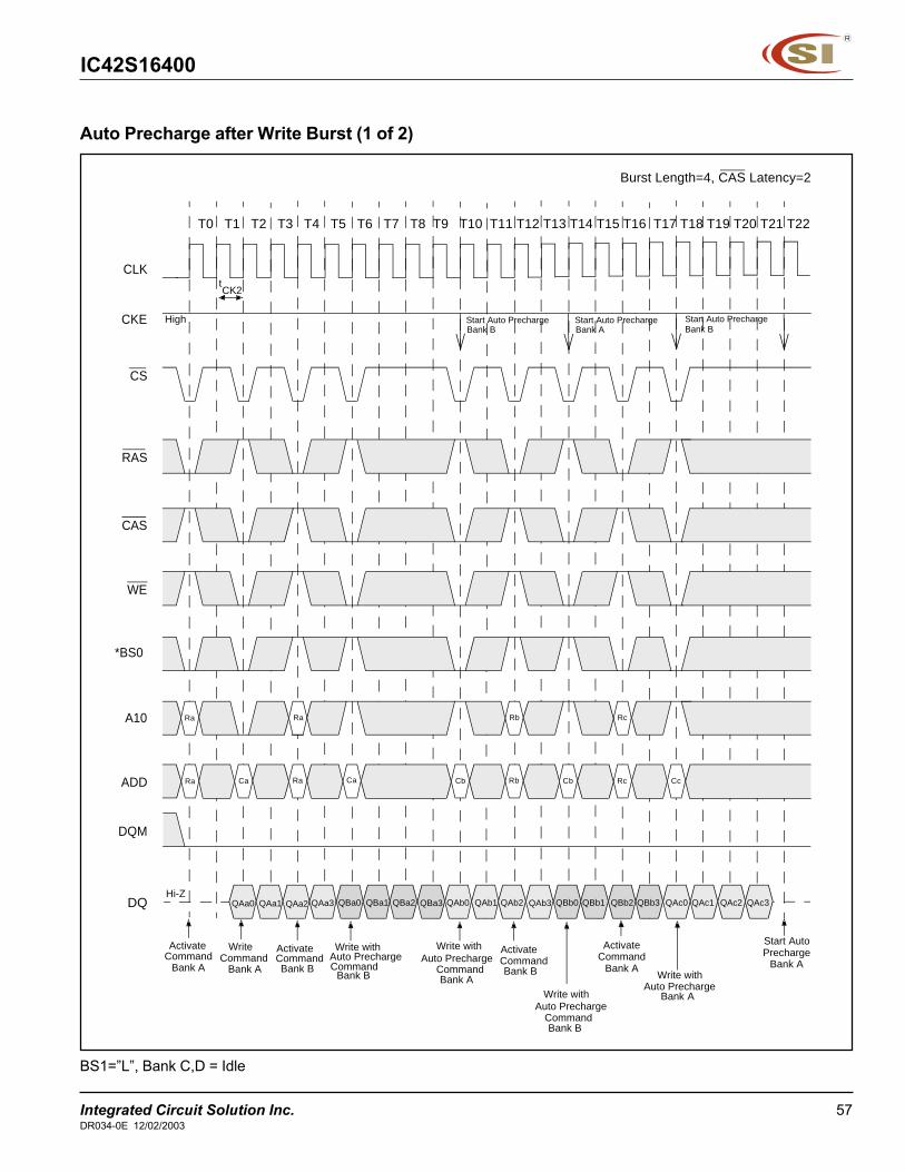
Auto Precharge after Write Burst (1 of 2)
BS1=”L”, Bank C,D = Idle
T0 T1 T2 T3 T4 T5 T6 T7 T8 T9 T10 T11 T12 T13 T14 T15 T16 T17 T18 T19 T20 T21 T22
CLK
CKE
CS
RAS
CAS
WE
A10
ADD
DQM
DQ
tCK2
Burst Length=4, CAS Latency=2
Activate
Bank ACommand
Hi-Z QBa3 QBb0QAa0 QAa1 QAa2 QAa3 QBa0 QBa1 QBb1
Ra Ra
Ra
QAb3QAb0 QAb1
Write Command
Bank A
Write with
CommandBank B
QBa2 QAb2
Write with
CommandBank A
ActivateCommandBank B
Write with
CommandBank B
Activate Command
Bank B
QBb2 QBb3
Rb
Ra Ca Cb Ca Rb Cb
Auto Precharge Auto Precharge
Auto Precharge
Start Auto PrechargeBank B
Start Auto PrechargeBank A
Start Auto PrechargeBank B
High
Rc
Rc Cc
QAc0 QAc1 QAc2 QAc3
ActivateCommand
Bank AWrite with
Auto PrechargeBank A
Start AutoPrecharge
Bank A
*BS0

IC42S16400
58 Integrated Circuit Solution Inc.DR034-0E 12/02/2003
Auto Precharge after Write Burst (2 of 2)
BS1=”L”, Bank C,D = Idle
T0 T1 T2 T3 T4 T5 T6 T7 T8 T9 T10 T11 T12 T13 T14 T15 T16 T17 T18 T19 T20 T21 T22
CLK
CKE
CS
RAS
CAS
WE
A10
ADD
DQM
DQ
tCK3
Burst Length=4, CAS Latency=3
Activate
Bank ACommand
Hi-Z QBa3QAa0 QAa1 QAa2 QAa3 QBa0 QBa1
Ra Ra
Ra
QAb3QAb0 QAb1
Read Command
Bank A
Read with
CommandBank B
QBa2 QAb2
CommandBank A
Activate Command
Bank B
QBb0
Ra Ca Ca RBb Cb
Auto Precharge
Start Auto PrechargeBank B
Start Auto
Bank A
Start Auto PrechargeBank B
High
Rb
Cb
QBb1 QBb2
ActivateCommand
Bank B
Write with
Auto PrechargeAuto precharge
CommandBank B
Read with
Rb
Precharge
QBb3
*BS0

IC42S16400
Integrated Circuit Solution Inc. 59DR034-0E 12/02/2003
Full Page Read Cycle (1 of 2)
BS1=”L”, Bank C,D = Idle
T0 T1 T2 T3 T4 T5 T6 T7 T8 T9 T10 T11 T12 T13 T14 T15 T16 T17 T18 T19 T20 T21 T22
CLK
CKE
CS
RAS
CAS
WE
A10
ADD
DQM
DQ
tCK2
Burst Length=Full Page, CAS Latency=2
Activate
Bank ACommand
Read
Hi-Z
Command
Ra
QAa+1
Bank A
The burst counter wraps Burst Stop
Read Command
Bank B
QAa
Full page burst operation does not
Ra Ca Rb
tRP
High
ActivateCommandBank B
Ra Rb
Ca
QAa+2 QAa-2 QAa-1 QAa QAa+1 QBa QBa+1 QBa+2 QBa+3 QBa+4 QBa+51QBa+6
Activate Command
Bank B
from the highest orderpage address back to zeroduring this time interval
terminate when the burst length is satisfied; the burst counterincrements and continues burstingbeginning with the starting address
Command
PrechargeCommand Bank B
Ra
*BS0

IC42S16400
60 Integrated Circuit Solution Inc.DR034-0E 12/02/2003
Full Page Read Cycle (2 of 2)
BS1=”L”, Bank C,D = Idle
T0 T1 T2 T3 T4 T5 T6 T7 T8 T9 T10 T11 T12 T13 T14 T15 T16 T17 T18 T19 T20 T21 T22
CLK
CKE
CS
RAS
CAS
WE
A10
ADD
DQM
DQ
tCK3
Burst Length=Full Page, CAS Latency=3
Activate
Bank ACommand
Read
Hi-Z
Command
Ra
QAa+1
Bank A
The burst counter wraps Burst Stop
Read Command
Bank B
QAa
Full page burst operation
Ra Ca Rb
High
ActivateCommandBank B
Ra Rb
Ca
QAa+2 QAa-2 QAa-1 QAa QAa+1 QBa0 QBa+1 QBa+2 QBa+3 QBa+4 QBa+5
Activate Command
Bank B
from the highest orderpage address back to zeroduring this time interval
Command
PrechargeCommand Bank B
does not teminate whenthe burst length is satisfied; the burst counter incrementsand continues bursting beginning with the starting address
Ra
*BS0

IC42S16400
Integrated Circuit Solution Inc. 61DR034-0E 12/02/2003
Full Page Write Cycle (1 of 2)
BS1=”L”, Bank C,D = Idle
T0 T1 T2 T3 T4 T5 T6 T7 T8 T9 T10 T11 T12 T13 T14 T15 T16 T17 T18 T19 T20 T21 T22
CLK
CKE
CS
RAS
CAS
WE
A10
ADD
DQM
DQ
tCK2
Burst Length=Full Page, CAS Latency=2
Activate
Bank ACommand
Write
Hi-Z
Command
Ra
QAa+1
Bank A
The burst counter wraps Burst Stop
Write Command
Bank B
QAa
Full page burst operation
Ra Ca Rb
tBDL
High
ActivateCommandBank B
Ra Rb
Ca
QAa+2 QAa+3 QAa-1 QAa QAa+1 QBa QBa+1 QBa+2 QBa+3 QBa+4 QBa+5
Activate Command
Bank B
from the highest orderpage address back to zeroduring this time interval
Command
PrechargeCommand Bank B
does not terminate whenthe burst length is satisfied; the burst counter incrementsand continues bursting beginning with the starting address
QBa+6
Data is ignored
Ra
*BS0

IC42S16400
62 Integrated Circuit Solution Inc.DR034-0E 12/02/2003
Full Page Write Cycle (2 of 2)
BS1=”L”, Bank C,D = Idle
T0 T1 T2 T3 T4 T5 T6 T7 T8 T9 T10 T11 T12 T13 T14 T15 T16 T17 T18 T19 T20 T21 T22
CLK
CKE
CS
RAS
CAS
WE
A10
ADD
DQM
DQ
tCK3
Burst Length=Full Page, CAS Latency=3
Activate
Bank ACommand
Write
Hi-Z
Command
Ra
DAa+1
Bank A
The burst counter wrapsBurst Stop
Write Command
Bank B
DAa
Full page burst operation
Ra
tBDL
High
ActivateCommandBank B
DAa+2 DAa+3 DAa-1 DAa DAa+1 DBa DBa+1 DBa+2 DBa+3 DBa+4 DBa+5
Activate Command
Bank B
from the highest orderpage address back to zeroduring this time interval
Command
PrechargeCommand Bank B
does not terminate whenthe burst length is satisfied; the burst counter incrementsand continues bursting beginning with the starting address
Ra Rb
Ca Ra Ca Rb
Data is ignored.
*BS0

IC42S16400
Integrated Circuit Solution Inc. 63DR034-0E 12/02/2003
Burst Read and Single Write Operation
BS1=”L”, Bank C,D = Idle
Hi-Z
T0 T1 T2 T3 T4 T5 T6 T7 T8 T9 T10 T11 T12 T13 T14 T15 T16 T17 T18 T19 T20 T21 T22
CLK
CKE
CS
RAS
CAS
WE
A10
ADD
DQM
tCK2
Burst Length=4, CAS Latency=2
RAa
RAa
High
Activate
CAa CAb CAd
DQ
CommandBank A
ReadCommand
Bank A
Single Write Single Write ReadCommand
Bank A
DQs are masked
CAc CAe
CommandBank A
CommandBank A
Single WriteCommandBank A
DQs are masked
*BS0

IC42S16400
64 Integrated Circuit Solution Inc.DR034-0E 12/02/2003
Full Page Random Column Read
BS1=”L”, Bank C,D = Idle
T0 T1 T2 T3 T4 T5 T6 T7 T8 T9 T10 T11 T12 T13 T14 T15 T16 T17 T18 T19 T20 T21 T22
CLK
CKE
CS
RAS
CAS
WE
BS
A10
ADD
DQM
DQ
tCK2
Burst Length=Full Page, CAS Latency=2
Activate
Bank ACommand
Activate
Hi-Z
Command
Ra
QBa0
Bank B
Read Command
Bank B
QAa0
Ra
ActivateCommandBank B
QAb0 QAb1 QBb0 QBb1 QAc0 QAc1 QAc2 QBc0 QBc1 QBc2
Read Command
Bank A
Precharge
Cc Cc Rb
Ra
Ra Ca Ca Cb Cb
Rb
tRP
Read Command
Bank B
Read Command
Bank A
Read Command
Bank A
Read Command
Bank BCommand Bank B
(Precharge Termination)(Bank D)

IC42S16400
Integrated Circuit Solution Inc. 65DR034-0E 12/02/2003
Full Page Random Column Write
BS1=”L”, Bank C,D = Idle
T0 T1 T2 T3 T4 T5 T6 T7 T8 T9 T10 T11 T12 T13 T14 T15 T16 T17 T18 T19 T20 T21 T22
CLK
CKE
CS
RAS
CAS
WE
A10
ADD
DQM
DQ
tCK2
Burst Length=Full Page, CAS Latency=2
Activate
Bank ACommand
Activate
Hi-Z
Command
Ra
QBa0
Bank B
Write Command
Bank B
QAa0
Ra
ActivateCommandBank B
QAb0 QAb1 QBb0 QBb1 QAc0 QAc1 QAc2 QBc0 QBc1 QBc2
Write Command
Bank A
Precharge
Cc Cc Rb
Ra
Ra Ca Ca Cb Cb
Rb
tRP
Write Command
Bank B
Write Command
Bank A
Write Command
Bank A
Write Command
Bank BCommand Bank B(Precharge Termination)
Write Datais masked
(Bank D)
*BS0
IC42S16400
66 Integrated Circuit Solution Inc.DR034-0E 12/02/2003
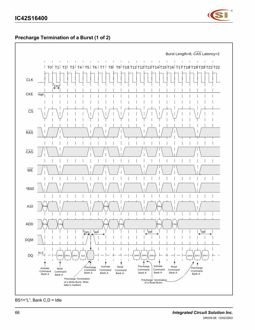
Precharge Termination of a Burst (1 of 2)
BS1=”L”, Bank C,D = Idle
T0 T1 T2 T3 T4 T5 T6 T7 T8 T9 T10 T11 T12 T13 T14 T15 T16 T17 T18 T19 T20 T21 T22
CLK
CKE
CS
RAS
CAS
WE
A10
ADD
DQM
DQ
tCK2
Burst Length=8, CAS Latency=2
Activate
Bank ACommand
Write
Hi-Z
Command
RAa
Bank A
Activate Command
Bank A
ReadCommandBank A
RAc CAb
RAb
RAb
RAc
Precharge Termination of a Write Burst. Writedata is masked.
PrechargeCommand
Read Command
Bank A
Precharge Command
Bank A
Precharge Termination
High
RAa CAcCAa
QAa1QAa0 QAa2 Da3 QAb0 QAb1 QAb2 QAc0 QAc1 QAc2
tDPL
tRP
tRP
tRP
Bank A
of a Read Burst.
Activate Command
Bank A
PrechargeCommandBank A
*BS0

IC42S16400
Integrated Circuit Solution Inc. 67DR034-0E 12/02/2003
Precharge Termination of a Burst (2 of 2)
BS1=”L”, Bank C,D = Idle
T0 T1 T2 T3 T4 T5 T6 T7 T8 T9 T10 T11 T12 T13 T14 T15 T16 T17 T18 T19 T20 T21 T22
CLK
CKE
CS
RAS
CAS
WE
A10
ADD
DQM
DQ
tCK3
Activate
Bank ACommand
Write
Hi-Z
Command
RAa
Bank A
Activate Command
Bank A
CAb
RAb
RAb
RAc
PrechargeCommand
Read Command
Bank A
High
RAa RAcCAa
DAa1DAa0 QAb0 QAb1 QAb2 QAb3
tDPL tRP
Bank A
Activate Command
Bank A
ActivateCommandBank A
tRCD
tRP
Write Datais masked
Precharge Terminationof a Write Burst.
Precharge Terminationof a Read Burst.
tRAS
*BS0
Burst Length=8, CAS Latency=3

IC42S16400
68 Integrated Circuit Solution Inc.DR034-0E 12/02/2003
ORDERING INFORMATIONCommercial Range: 0οοοοοC to 70οοοοοC
Speed (ns) Order Part No. Package6 IC42S16400-6T 400mil TSOP-2
IC42S16400-6TG 400mil TSOP-2(Pb-free)IC42S16400-6BG 60Ball VF-BGA(Pb-free)
7 IC42S16400-7T 400mil TSOP-2IC42S16400-7TG 400mil TSOP-2(Pb-free)IC42S16400-7BG 60Ball VF-BGA(Pb-free)
ORDERING INFORMATIONIndustrial Temperature Range: -40οοοοοC to 85οοοοοC
Speed (ns) Order Part No. Package6 IC42S16400-6TI 400mil TSOP-2
IC42S16400-6TIG 400mil TSOP-2(Pb-free)IC42S16400-6BIG 60Ball VF-BGA(Pb-free)
7 IC42S16400-7TI 400mil TSOP-2IC42S16400-7TIG 400mil TSOP-2(Pb-free)IC42S16400-7BIG 60Ball VF-BGA(Pb-free)
Integrated Circuit Solution Inc.HEADQUARTER:
NO.2, TECHNOLOGY RD. V, SCIENCE-BASED INDUSTRIAL PARK,HSIN-CHU, TAIWAN, R.O.C.
TEL: 886-3-5780333Fax: 886-3-5783000
BRANCH OFFICE:7F, NO. 106, SEC. 1, HSIN-TAI 5TH ROAD,
HSICHIH TAIPEI COUNTY, TAIWAN, R.O.C. TEL: 886-2-26962140FAX: 886-2-26962252
http://www.icsi.com.tw