41st IEEE Semiconductor Interface Specialists Conference · 41st IEEE . Semiconductor Interface ....
25
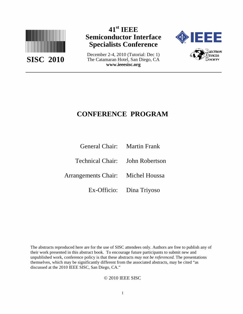
1 41 st IEEE Semiconductor Interface Specialists Conference December 2-4, 2010 (Tutorial: Dec 1) The Catamaran Hotel, San Diego, CA www.ieeesisc.org CONFERENCE PROGRAM General Chair: Martin Frank Technical Chair: John Robertson Arrangements Chair: Michel Houssa Ex-Officio: Dina Triyoso The abstracts reproduced here are for the use of SISC attendees only. Authors are free to publish any of their work presented in this abstract book. To encourage future participants to submit new and unpublished work, conference policy is that these abstracts may not be referenced. The presentations themselves, which may be significantly different from the associated abstracts, may be cited “as discussed at the 2010 IEEE SISC, San Diego, CA.” © 2010 IEEE SISC SISC 2010
Transcript of 41st IEEE Semiconductor Interface Specialists Conference · 41st IEEE . Semiconductor Interface ....
1
41st IEEE
Semiconductor Interface Specialists Conference
December 2-4, 2010 (Tutorial: Dec 1) The Catamaran Hotel, San Diego, CA
www.ieeesisc.org
CONFERENCE PROGRAM
General Chair: Martin Frank
Technical Chair: John Robertson
Arrangements Chair: Michel Houssa
Ex-Officio: Dina Triyoso
The abstracts reproduced here are for the use of SISC attendees only. Authors are free to publish any of their work presented in this abstract book. To encourage future participants to submit new and unpublished work, conference policy is that these abstracts may not be referenced. The presentations themselves, which may be significantly different from the associated abstracts, may be cited “as discussed at the 2010 IEEE SISC, San Diego, CA.”
© 2010 IEEE SISC
SISC 2010
2
41st IEEE
Semiconductor Interface Specialists Conference
December 2-4, 2010 (Tutorial: Dec 1) The Catamaran Hotel, San Diego, CA
www.ieeesisc.org
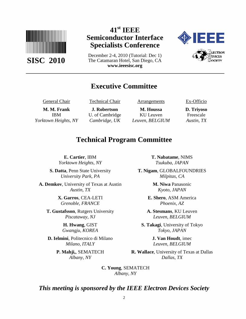
Executive Committee
General Chair Technical Chair Arrangements Ex-Officio
M. M. Frank IBM
Yorktown Heights, NY
J. Robertson U. of Cambridge Cambridge, UK
M. Houssa KU Leuven
Leuven, BELGIUM
D. Triyoso Freescale Austin, TX
Technical Program Committee
E. Cartier, IBM Yorktown Heights, NY
T. Nabatame, NIMS Tsukuba, JAPAN
S. Datta, Penn State University University Park, PA
T. Nigam, GLOBALFOUNDRIES Milpitas, CA
A. Demkov, University of Texas at Austin Austin, TX
M. Niwa Panasonic Kyoto, JAPAN
X. Garros, CEA-LETI Grenoble, FRANCE
E. Shero, ASM America Phoenix, AZ
T. Gustafsson, Rutgers University Piscataway, NJ
A. Stesmans, KU Leuven Leuven, BELGIUM
H. Hwang, GIST Gwangju, KOREA
S. Takagi, University of Tokyo Tokyo, JAPAN
D. Ielmini, Politecnico di Milano Milano, ITALY
J. Van Houdt, imec Leuven, BELGIUM
P. Mahji,, SEMATECH Albany, NY
R. Wallace, University of Texas at Dallas Dallas, TX
C. Young, SEMATECH Albany, NY
This meeting is sponsored by the IEEE Electron Devices Society
SISC 2010
3
41st IEEE
Semiconductor Interface Specialists Conference
December 2-4, 2010 (Tutorial: Dec 1) The Catamaran Hotel, San Diego, CA
www.ieeesisc.org
SISC Ed Nicollian Award for Best Student Paper
In 1995, the SISC began presenting an award for the best student presentation, in honor of
Professor E.H. Nicollian, University of North Carolina at Charlotte. Professor Nicollian was a
pioneer in the exploration of the metal-oxide-semiconductor system, particularly in the area of
electrical measurements. His efforts were fundamental in establishing the SISC in its early years,
and he served as its technical program chair in 1982. With John Brews, he wrote the definitive
book, “MOS Physics and Technology,” published by Wiley Interscience.
The SISC Ed Nicollian Award for Best Student Paper is presented to the lead student author or
either an oral or poster presentation. The winner is chosen by members of the technical program
committee at the end of the SISC. The award consists of a plaque, an honorarium, and a
permanent mention on the conference web site.
Winner of the 2009 SISC Ed Nicollian Award for Best Student Paper:
Jacopo Franco, imec, Leuven, and KU Leuven, Belgium
“Impact of Si-Passivation Thickness and Processing
on NBTI Reliability of Ge and SiGe pMOSFETs”
with B. Kaczer, A. Stesmans, V. V. Afanas'ev, K. Martens,
M. Aoulaiche, T. Grasser, J. Mitard, G. Groeseneken
SISC 2010
4
41st IEEE
Semiconductor Interface Specialists Conference
December 2-4, 2010 (Tutorial: Dec 1) The Catamaran Hotel, San Diego, CA
www.ieeesisc.org
Wednesday Evening Tutorial
Wednesday, December 1, 2010, 8:00 PM
First introduced at SISC 2008, the Wednesday evening Tutorial aims to provide a good
foundation in a topic frequently covered at the conference, particularly benefiting students and
newcomers to the field. The Tutorial is free to all registered SISC attendees.
Dr. Matthias Passlack
TSMC Europe, Leuven, Belgium
“Interface state analysis on non-silicon semiconductors and the role of heterostructures”
Non-silicon semiconductors are considered as alternative channel materials to enable and
facilitate CMOS scaling beyond silicon. Both materials comprising column IV (e.g. Ge) and
compounds formed from columns III and V (e.g. Ga, In, As, Sb) elements of the periodic table are
of interest. Electrical interface characterization which has been traditionally silicon centric needs
to embrace their different electronic properties to ensure accurate interface state analysis and to
exploit new opportunities. In a first part, this tutorial will propose a flow chart for admittance-
voltage characterization of interfaces formed between dielectrics and alternate channel materials
commencing with basic physics and concluding with selection of measurements parameters and
models for trap quantification. During a second part, an interface characterization technique
suitable for direct bandgap semiconductors and relying on carrier recombination
(photoluminescence intensity) is discussed. Finally, exploitation of heterostructures at
dielectric/semiconductor interfaces and related implications for the impact of interface states on
device performance are examined.
SISC 2010
5
41st IEEE
Semiconductor Interface Specialists Conference
December 2-4, 2010 (Tutorial: Dec 1) The Catamaran Hotel, San Diego, CA
www.ieeesisc.org
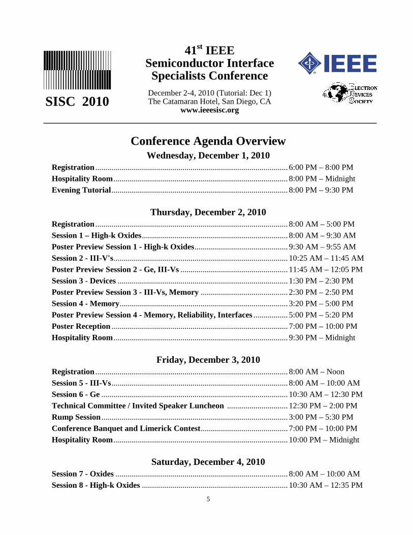
Conference Agenda Overview Wednesday, December 1, 2010
Registration ............................................................................................... 6:00 PM – 8:00 PM Hospitality Room ...................................................................................... 8:00 PM – Midnight Evening Tutorial ....................................................................................... 8:00 PM – 9:30 PM
Thursday, December 2, 2010 Registration ............................................................................................... 8:00 AM – 5:00 PM Session 1 – High-k Oxides ........................................................................ 8:00 AM – 9:30 AM
Poster Preview Session 1 - High-k Oxides .............................................. 9:30 AM – 9:55 AM
Session 2 - III-V's ...................................................................................... 10:25 AM – 11:45 AM Poster Preview Session 2 - Ge, III-Vs ..................................................... 11:45 AM – 12:05 PM Session 3 - Devices .................................................................................... 1:30 PM – 2:30 PM Poster Preview Session 3 - III-Vs, Memory ........................................... 2:30 PM – 2:50 PM Session 4 - Memory ................................................................................... 3:20 PM – 5:00 PM Poster Preview Session 4 - Memory, Reliability, Interfaces ................. 5:00 PM – 5:20 PM Poster Reception ....................................................................................... 7:00 PM – 10:00 PM Hospitality Room ...................................................................................... 9:30 PM – Midnight
Friday, December 3, 2010 Registration ............................................................................................... 8:00 AM – Noon Session 5 - III-Vs ....................................................................................... 8:00 AM – 10:00 AM
Session 6 - Ge ............................................................................................ 10:30 AM – 12:30 PM Technical Committee / Invited Speaker Luncheon .............................. 12:30 PM – 2:00 PM Rump Session ............................................................................................ 3:00 PM – 5:30 PM Conference Banquet and Limerick Contest ........................................... 7:00 PM – 10:00 PM Hospitality Room ...................................................................................... 10:00 PM – Midnight
Saturday, December 4, 2010 Session 7 - Oxides ..................................................................................... 8:00 AM – 10:00 AM
Session 8 - High-k Oxides ........................................................................ 10:30 AM – 12:35 PM
SISC 2010
6
41st IEEE
Semiconductor Interface Specialists Conference
December 2-4, 2010 (Tutorial: Dec 1) The Catamaran Hotel, San Diego, CA
www.ieeesisc.org
Conference Program
Session 1 - High-k Oxides Thursday, December 2, 2010 Session Chair: M. M. Frank
8:00 AM Welcome and opening remarks 8:15 AM 1.1 Invited - Materials and Processes for High-k Metal Gate Stacks for 28 nm
and Beyond, P. Kirsch, SEMATECH 8:50 AM 1.2 - Kinetics of Interfacial Layer Scavenging and Dipole Formation for
Ultimate Scaling of Hf-based High-k Gate Dielectrics, T. Ando1, H. Arimura2, R. Haight1, M. Copel1, H. Watanabe2, and V. Narayanan1, 1IBM, 2Osaka University, Japan
9:10 AM 1.3 - Study of Trap Distribution in Ultra-thin Dielectrics by Inelastic Electron Tunneling Spectroscopy, Z. Liu, S. Cui, and T.P. Ma, Yale University
Poster Preview Session 1 - High-k Oxides Thursday, December 2, 2010 Session Chair: M. M. Frank
9:30 AM Poster Introduction
9:35 AM P.1 - Passivation of High-k Bulk and Interface Defects by Incorporating La into Hf-silicate and its Impact on Carrier Mobility, M. Saeki, H. Arimura, N. Kitano, T. Hosoi, T. Shimura, and H. Watanabe, Osaka University, Japan
P.2 - Interfacial Design of High-k/Ge Gate Stacks with ZrO2 Dielectrics for Scaled Ge-based MOS Devices, T. Hosoi1, G. Okamoto1, I. Hideshima1, A. Kasuya1, K. Kutsuki1, J. Harries2, A. Yoshigoe2, Y. Teraoka2, T. Shimura1, and H. Watanabe1, 1Osaka University, Japan, 2Japan Atomic Energy Agency, Japan
SISC 2010
7
P.3 - Innovative Characterization Methods to Investigate High-k Metal Gate Stack Work Function, M. Charbonnier1, C. Leroux1, G. Ghibaudo2, F. Martin1, H. Grampeix1, F. Boulanger1, and G. Reimbold1, 1CEA-LETI-MINATEC, France, 2IMEP Minatec, France
P.4 - First Principles Investigation of Flat-Band Shift in a Lanthanum Doped Gate Stack Si/SiO2/HfO2:La2O3, E. Nadimi1, R. Öttking2, P. Plänitz2, M. Trentzsch3, T. Kelwing3, R. Carter3, and C. Radehaus2, 1Technische Universität Chemnitz, Germany, 2GWT–TUD GmbH, Germany, 3Global Foundries, Germany
P.5 - The Role of Oxygen in High-k/SiO2 Interfacial Dipoles on the Schottky Barrier Height at Metal-Semiconductor Interfaces, B. E. Coss1, W.-Y. Loh2, P. Majhi2, R. Jammy2, R. M. Wallace1, and J. Kim1, 1UT Dallas, 2SEMATECH
P.6 - A Comparative Study on the Effect of Post Deposition Annealing on the Physical Property and Electrical Reliability of Hf1-xZrxOy Gate Dielectrics, H.-S. Jung1,2, S. Y. Lee1, S.-H. Rha1, H. K. Kim1, Y. J. Chung1, J.-M. Park2, W.-H. Kim2, M.-W. Song2, N.-I. Lee2, and C. S. Hwang1, 1Seoul National University, Korea, 2Samsung, Korea
P.7 - Charge Trapping in LaLuO3 MOS Capacitors Using a New 3-Pulse CV Technique, N. Sedghi1, W. Davey1, I. Z. Mitrovic1, S. Hall1, J. M. J. Lopes2, and J. Schubert2, 1University of Liverpool, UK, 2Research Centre Jülich, Germany
P.8 - Integration of LaLuO3/TiN Gate Stack in Strained-SiGe p-MOSFETs, W. Yu1,2, B. Zhang1,2, Q. T. Zhao1, J.-M. Hartmann3, D. Buca1, A. Nichau1, J. M. J. Lopes1, J.Schubert1, K. Bourdelle4, X. Wang2, and S. Mantl1, 1Research Centre Jülich, Germany, 2Chinese Academy of Sciences, China, 3CEA-LETI-MINATEC, France, 4SOITEC, France
P.9 - Energy Spin Dependent Trap Assisted Tunneling in Gd2O3 Dielectrics, B. C. Bittel1, P. M. Lenahan1, E. Lipp2, and M. Eizenberg2, 1The Pennsylvania State University, 2Technion-Israel Institute of Technology, Israel
P.10 - Monolayer Passivation of Ge(100) Surface via Nitridation and Oxidation, J. S. Lee, S. R. Bishop, T. Kaufman-Osborn, E. A. Chagarov, and A. C. Kummel, UC San Diego
P.11 - Crystallization of Thick Amorphous GeO2 on Ge to α-quartz Structure - Experimental Evidence and Crystallization Model, S. K. Wang1, K. Kita1,2, T. Nishimura1,2, K. Nagashio1,2, and A. Toriumi1,2, 1The University of Tokyo, Japan, 2JST-CREST, Japan
P.12 - Impact of Low Temperature O2 Annealing for Stabilizing LaLuO3/Ge Gate Stacks without Additional Interface Layer Formation, T. Tabata1,2, C. H. Lee1, T. Nishimura1,2, K. Kita1,2, and A. Toriumi1,2, 1The University of Tokyo, Japan, 2JST-CREST, Japan
9:55 AM Break
8
Session 2 - III-V's Thursday, December 2, 2010 Session Chair: R. M. Wallace
10:25 AM Opening remarks
10:30 AM 2.1 Invited - High Performance InGaAs Quantum Well FETs with High-k Dielectrics, M. Radosavljevic, Intel
11:05 AM 2.2 - Calculation of Electron and Hole Mobility in Inversion Layers of MOS Systems with III-V Channels and High-k Insulators, T. O'Regan, Y. Zhang, and M. V. Fischetti, University of Massachusetts Amherst
11:25 AM 2.3 - Self-Aligned Gate-First In0.7Ga0.3As N-MOSFETs with an InP Capping Layer for Performance Enhancement, X. Gong, Ivana, H.-C. Chin, Z. Zhu, and Y.-C. Yeo, National University of Singapore, Singapore
Poster Preview Session 2 - Ge, III-Vs Thursday, December 2, 2010 Session Chair: R. M. Wallace
11:45 AM P.13 - Atomic Structures, Models, and Band Offsets of Ge:GeO:GeO2 Interfaces, L. Lin1, J. Robertson1, and K. Xiong2, 1University of Cambridge, UK, 2UT Dallas
P.14 - Energetics of Hydrogen in Ge and GeO2 Interfaces, K. Xiong1, L. Lin2, J. Robertson2, and K. Cho1, 1UT Dallas, 2University of Cambridge, UK
P.15 - Fermi Level De-pinning of Aluminium Contacts to Germanium Using Thin ALD Al2O3 Interfacial Layer, D. R. Gajula1, D. Tantraviwat1, Y. H. Low1, P. T. Baine1, M. Modreanu2, B. M. Armstrong1, and D. W. McNeill1, 1Queen’s University Belfast, UK, 2Tyndall National Institute, Ireland
P.16 - ALD Temperature Dependence of Slow Trap Properties at ALD-Al2O3/InP Interfaces, N. Taoka1, M. Yokoyama1, S. H. Kim1, T. Hoshii1, R. Iida1, S. Lee1, R. Suzuki1, Y. Urabe2, N. Miyata2, T. Yasuda2, H. Yamada3, N. Fukuhara3, M. Hata3, M. Takenaka1, and S. Takagi1, 1The University of Tokyo, Japan, 2National Institute of Advanced Industrial Science and Technology (AIST), Japan, 3Sumitomo Chemical Co., Japan
P.17 - Passivation of InGaAs and InAs by ALD Precursors, E. A. Chagarov1, J. B. Clemens1, M. Holland2, R. Droopad3, J. Shen1, and A. C. Kummel1, 1UC San Diego, 2University of Glasgow, UK, 3Texas State University-San Marcos
P.18 - Interfacial Layer Defect Response of Metal/High-k/GaAs C-V Characteristics, A. M. Sonnet, C. L. Hinkle, and E. M. Vogel, UT Dallas
9
P.19 - Low Temperature ALD Growth of Al2O3 Gate Dielectric for GaSb pMOSFETs, M. Xu and P. D. Ye, Purdue University
P.20 - Band Alignment at Interfaces of (100)InP with Atomic-Layer Deposited Al2O3, V. V. Afanas’ev1, Hsing-Yi Chou1, A. Stesmans1, D. Lin2, P. K. Hurley3, and S. B. Newcomb4, 1KU Leuven, Belgium, 2imec, Belgium, 3Tyndall National Institute, Ireland, 4Glebe Scientific Ltd., Ireland
P.21 - Infrared Spectroscopic Characterization of Wet Chemical Processes and Trimethylaluminum Treatments of III-V Surfaces, W. Cabrera, and Y. Chabal, UT Dallas
P.22 - In-situ Atomic Layer Deposition-Al2O3 on Freshly MBE Grown GaAs, M. L. Huang1, Y. H. Chang1, P. Chang1, C. A. Lin1, J. Kwo1, T.-W. Pi2, and M. Hong1, 1National Tsing Hua University, Taiwan, 2National Synchrotron Radiation Research Center, Taiwan
P.23 - Interfacial Electronic Structure of Ga2O3(Gd2O3) Grown on n-Ge Studied by Synchrotron Radiation Photoemission, T.-W. Pi1, W. C. Lee2, M. L. Huang2, L. K. Chu2, T. D. Lin2, T. H. Chiang2, Y. C. Wang2,J. Kwo2, and M. Hong2, 1National Synchrotron Radiation Research Center, Taiwan, 2National Tsing Hua University, Taiwan
P.24 - InGaAs Channel IFQW-MOSFET: Effect of InAlAs Interfacial Passivation Layer and (NH4)2S Treatment on the Electrical Behavior, A. Alian1,2, C. Merckling1, G. Brammertz1, M. Meuris1, K. De Meyer1,2, M. Heyns1,2, and T. Y. Hoffmann1, 1imec, Belgium, 2KU Leuven, Belgium
12:05 AM Adjourn for lunch
Session 3 - Devices Thursday, December 2, 2010
Session Chair: S. Takagi 1:30 PM Opening remarks 1:35 PM 3.1 Invited - Nanowire Transistors: Performance Limits, Strain Engineering,
Reduction of Parasitic Resistance, Y.-C. Yeo, National University of Singapore, Singapore
2:10 PM 3.2 - InAs and In0.7Ga0.3As Buried Channel MOSFETs with ALD Gate Dielectrics, F. Xue, H. Zhao, Y. Chen, Y. Wang, F. Zhou, and J. Lee, UT Austin
10
Poster Preview Session 3 - III-Vs, Memory Thursday, December 2, 2010
Session Chair: X. Garros
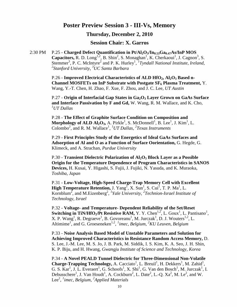
2:30 PM P.25 - Charged Defect Quantification in Pt/Al2O3/In0.53Ga0.47As/InP MOS Capacitors, R. D. Long1,2, B. Shin2, S. Monaghan1, K. Cherkaoui1, J. Cagnon3, S. Stemmer3, P. C. McIntyre2 and P. K. Hurley1, 1Tyndall National Institute, Ireland, 2Stanford University, 3UC Santa Barbara
P.26 - Improved Electrical Characteristics of ALD HfO2, Al2O3 Based n-Channel MOSFETs on InP Substrate with Postgate SF6 Plasma Treatment, Y. Wang, Y.-T. Chen, H. Zhao, F. Xue, F. Zhou, and J. C. Lee, UT Austin
P.27 - Origin of Interfacial Gap States in Ga2O3 Layer Grown on GaAs Surface and Interface Passivation by F and Gd, W. Wang, R. M. Wallace, and K. Cho, 1UT Dallas
P.28 - The Effect of Graphite Surface Condition on Composition and Morphology of ALD Al2O3, A. Pirkle1, S. McDonnell1, B. Lee1, J. Kim1, L. Colombo2, and R. M. Wallace1, 1UT Dallas, 2Texas Instruments
P.29 - First Principles Study of the Energetics of Ideal GaAs Surfaces and Adsorption of Al and O as a Function of Surface Oorientation, G. Hegde, G. Klimeck, and A. Strachan, Purdue University
P.30 - Transient Dielectric Polarization of Al2O3 Block Layer as a Possible Origin for the Temperature Dependence of Program Characteristics in SANOS Devices, H. Kusai, Y. Higashi, S. Fujii, J. Fujiki, N. Yasuda, and K. Muraoka, Toshiba, Japan
P.31 - Low-Voltage, High-Speed Charge-Trap Memory Cell with Excellent High Temperature Retention, J. Yang1, X. Sun1, S. Cui1, T. P. Ma1, L. Kornblum2, and M.Eizenberg2, 1Yale University, 2Technion-Israel Institute of Technology, Israel
P.32 - Voltage- and Temperature- Dependent Reliability of the Set/Reset Switching in TiN/HfO2/Pt Resistive RAM, Y. Y. Chen1,2, L. Goux1, L. Pantisano1, X. P. Wang1, R. Degraeve1, B. Govoreanu1, M. Jurczak1, D. J. Wouters1,2, L. Altimime1, and G. Groeseneken1,2, 1imec, Belgium, 2KU Leuven, Belgium
P.33 - Noise Analysis Based Model of Unstable Parameters and Solution for Achieving Improved Characteristics in Resistance Random Access Memory, D. S. Lee, J.-M. Lee, M. S. Jo, J. B. Park, M. Siddik, I. S. Kim, K. A. Seo, J. H. Shin, K. P. Biju, and H. Hwang, Gwangju Institute of Science and Technology, Korea
P.34 - A Novel PEALD Tunnel Dielectric for Three-Dimensional Non-Volatile Charge-Trapping Technology, A. Cacciato1, L. Breuil1, H. Dekkers1, M. Zahid1, G. S. Kar1, J. L. Everaert1, G. Schoofs1, X. Shi1, G. Van den Bosch1, M. Jurczak1, I. Debusschere1, J. Van Houdt1, A. Cockburn2, L. Date2, L.-Q. Xa2, M. Le2, and W. Lee2, 1imec, Belgium, 2Applied Materials
11
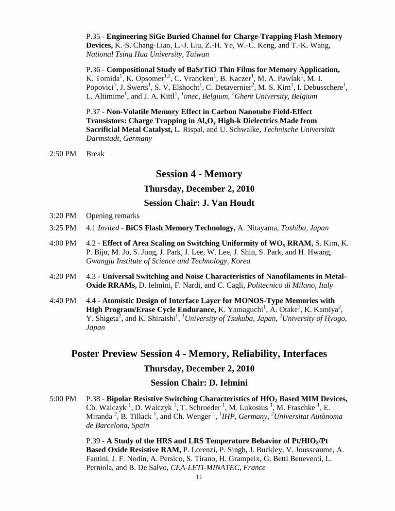
P.35 - Engineering SiGe Buried Channel for Charge-Trapping Flash Memory Devices, K.-S. Chang-Liao, L.-J. Liu, Z.-H. Ye, W.-C. Keng, and T.-K. Wang, National Tsing Hua University, Taiwan
P.36 - Compositional Study of BaSrTiO Thin Films for Memory Application, K. Tomida1, K. Opsomer1,2, C. Vrancken1, B. Kaczer1, M. A. Pawlak1, M. I. Popovici1, J. Swerts1, S. V. Elshocht1, C. Detavernier2, M. S. Kim1, I. Debusschere1, L. Altimime1, and J. A. Kittl1, 1imec, Belgium, 2Ghent University, Belgium
P.37 - Non-Volatile Memory Effect in Carbon Nanotube Field-Effect Transistors: Charge Trapping in AlxOy High-k Dielectrics Made from Sacrificial Metal Catalyst, L. Rispal, and U. Schwalke, Technische Universität Darmstadt, Germany
2:50 PM Break
Session 4 - Memory Thursday, December 2, 2010 Session Chair: J. Van Houdt
3:20 PM Opening remarks 3:25 PM 4.1 Invited - BiCS Flash Memory Technology, A. Nitayama, Toshiba, Japan
4:00 PM 4.2 - Effect of Area Scaling on Switching Uniformity of WOx RRAM, S. Kim, K. P. Biju, M. Jo, S. Jung, J. Park, J. Lee, W. Lee, J. Shin, S. Park, and H. Hwang, Gwangju Institute of Science and Technology, Korea
4:20 PM 4.3 - Universal Switching and Noise Characteristics of Nanofilaments in Metal-Oxide RRAMs, D. Ielmini, F. Nardi, and C. Cagli, Politecnico di Milano, Italy
4:40 PM 4.4 - Atomistic Design of Interface Layer for MONOS-Type Memories with High Program/Erase Cycle Endurance, K. Yamaguchi1, A. Otake1, K. Kamiya2, Y. Shigeta2, and K. Shiraishi1, 1University of Tsukuba, Japan, 2University of Hyogo, Japan
Poster Preview Session 4 - Memory, Reliability, Interfaces Thursday, December 2, 2010
Session Chair: D. Ielmini
5:00 PM P.38 - Bipolar Resistive Switching Characteristics of HfO2 Based MIM Devices, Ch. Walczyk 1, D. Walczyk 1, T. Schroeder 1, M. Lukosius 1, M. Fraschke 1, E. Miranda 2, B. Tillack 1, and Ch. Wenger 1, 1IHP, Germany, 2Universitat Autònoma de Barcelona, Spain
P.39 - A Study of the HRS and LRS Temperature Behavior of Pt/HfO2/Pt Based Oxide Resistive RAM, P. Lorenzi, P. Singh, J. Buckley, V. Jousseaume, A. Fantini, J. F. Nodin, A. Persico, S. Tirano, H. Grampeix, G. Betti Beneventi, L. Perniola, and B. De Salvo, CEA-LETI-MINATEC, France
12
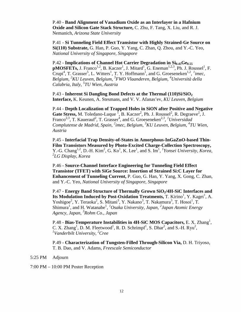
P.40 - Band Alignment of Vanadium Oxide as an Interlayer in a Hafnium Oxide and Silicon Gate Stack Structure, C. Zhu, F. Tang, X. Liu, and R. J. Nemanich, Arizona State University
P.41 - Si Tunneling Field Effect Transistor with Highly Strained-Ge Source on Si(110) Substrate, G. Han, P. Guo, Y. Yang, C. Zhan, Q. Zhou, and Y.-C. Yeo, National University of Singapore, Singapore
P.42 - Implications of Channel Hot Carrier Degradation in Si0.45Ge0.55 pMOSFETs, J. Franco1,2, B. Kaczer1, J. Mitard1, G. Eneman1,2,3, Ph. J. Roussel1, F. Crupi4, T. Grasser5, L. Witters1, T. Y. Hoffmann1, and G. Groeseneken1,2, 1imec, Belgium, 2KU Leuven, Belgium, 3FWO Vlaanderen, Belgium, 4Università della Calabria, Italy, 5TU Wien, Austria
P.43 - Inherent Si Dangling Bond Defects at the Thermal (110)Si/SiO2 Interface, K. Keunen, A. Stesmans, and V. V. Afanas’ev, KU Leuven, Belgium
P.44 - Depth Localization of Trapped Holes in SiON after Positive and Negative Gate Stress, M. Toledano-Luque 1, B. Kaczer2, Ph. J. Roussel2, R. Degraeve2, J. Franco2,3, T. Kauerauf2, T. Grasser4, and G. Groeseneken2,3, 1Universidad Complutense de Madrid, Spain, 2imec, Belgium, 3KU Leuven, Belgium, 4TU Wien, Austria
P.45 - Interfacial Trap Density-of-States in Amorphous-InGaZnO-based Thin-Film Transistors Measured by Photo-Excited Charge-Collection Spectroscopy, Y.-G. Chang1,2, D.-H. Kim2, G. Ko1, K. Lee1, and S. Im1, 1Yonsei University, Korea, 2LG Display, Korea
P.46 - Source-Channel Interface Engineering for Tunneling Field Effect Transistor (TFET) with SiGe Source: Insertion of Strained Si:C Layer for Enhancement of Tunneling Current, P. Guo, G. Han, Y. Yang, X. Gong, C. Zhan, and Y.-C. Yeo, National University of Singapore, Singapore
P.47 - Energy Band Structure of Thermally Grown SiO2/4H-SiC Interfaces and Its Modulation Induced by Post-Oxidation Treatments, T. Kirino1, Y. Kagei1, A. Yoshigoe2, Y. Teraoka2, S. Mitani3, Y. Nakano3, T. Nakamura3, T. Hosoi1, T. Shimura1, and H. Watanabe1, 1Osaka University, Japan, 2Japan Atomic Energy Agency, Japan, 3Rohm Co., Japan
P.48 - Bias-Temperature Instabilities in 4H-SiC MOS Capacitors, E. X. Zhang1, C. X. Zhang1, D. M. Fleetwood1, R. D. Schrimpf1, S. Dhar2, and S.-H. Ryu2, 1Vanderbilt University, 2Cree
P.49 - Characterization of Tungsten-Filled Through-Silicon Via, D. H. Triyoso, T. B. Dao, and V. Adams, Freescale Semiconductor
5:25 PM Adjourn
7:00 PM – 10:00 PM Poster Reception
13
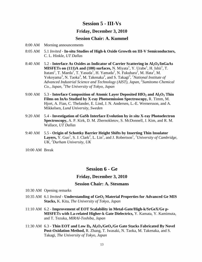
Session 5 - III-Vs Friday, December 3, 2010 Session Chair: A. Kummel
8:00 AM Morning announcements 8:05 AM 5.1 Invited - In-situ Studies of High-k Oxide Growth on III-V Semiconductors,
C. L. Hinkle, UT Dallas
8:40 AM 5.2 - Interface As Oxides as Indicator of Carrier Scattering in Al2O3/InGaAs MISFETs on (111)A and (100) surfaces, N. Miyata1, Y. Urabe1, H. Ishii1, T. Itatani1, T. Maeda1, T. Yasuda1, H. Yamada2, N. Fukuhara2, M. Hata2, M. Yokoyama3, N. Taoka3, M. Takenaka3, and S. Takagi3, 1National Institute of Advanced Industrial Science and Technology (AIST), Japan, 2Sumitomo Chemical Co., Japan, 3The University of Tokyo, Japan
9:00 AM 5.3 - Interface Composition of Atomic Layer Deposited HfO2 and Al2O3 Thin Films on InAs Studied by X-ray Photoemission Spectroscopy, R. Timm, M. Hjort, A. Fian, C. Thelander, E. Lind, J. N. Andersen, L.-E. Wernersson, and A. Mikkelsen, Lund University, Sweden
9:20 AM 5.4 - Investigation of GaSb Interface Evolution by in situ X-ray Photoelectron Spectroscopy, A. P. Kirk, D. M. Zhernokletov, S. McDonnell, J. Kim, and R. M. Wallace, UT Dallas
9:40 AM 5.5 - Origin of Schottky Barrier Height Shifts by Inserting Thin Insulator Layers, Y. Guo1, S. J. Clark2, L. Lin1, and J. Robertson1, 1University of Cambridge, UK, 2Durham University, UK
10:00 AM Break
Session 6 - Ge Friday, December 3, 2010
Session Chair: A. Stesmans 10:30 AM Opening remarks 10:35 AM 6.1 Invited - Understanding of GeO2 Material Properties for Advanced Ge MIS
Stacks, K. Kita, The University of Tokyo, Japan
11:10 AM 6.2 - Improvement of EOT Scalability in Metal-Gate/High-k/SrGeX/Ge p-MISFETs with La-related Higher-k Gate Dielectrics, Y. Kamata, Y. Kamimuta, and T. Tezuka, MIRAI-Toshiba, Japan
11:30 AM 6.3 - Thin EOT and Low Dit Al2O3/GeOx/Ge Gate Stacks Fabricated By Novel Post-Oxidation Method, R. Zhang, T. Iwasaki, N. Taoka, M. Takenaka, and S. Takagi, The University of Tokyo, Japan
14
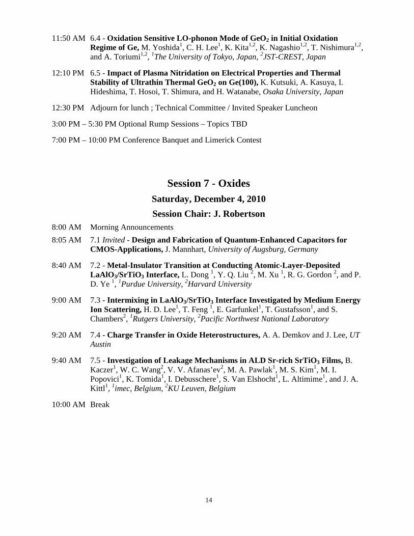
11:50 AM 6.4 - Oxidation Sensitive LO-phonon Mode of GeO2 in Initial Oxidation Regime of Ge, M. Yoshida1, C. H. Lee1, K. Kita1,2, K. Nagashio1,2, T. Nishimura1,2, and A. Toriumi1,2, 1The University of Tokyo, Japan, 2JST-CREST, Japan
12:10 PM 6.5 - Impact of Plasma Nitridation on Electrical Properties and Thermal Stability of Ultrathin Thermal GeO2 on Ge(100), K. Kutsuki, A. Kasuya, I. Hideshima, T. Hosoi, T. Shimura, and H. Watanabe, Osaka University, Japan
12:30 PM Adjourn for lunch ; Technical Committee / Invited Speaker Luncheon
3:00 PM – 5:30 PM Optional Rump Sessions – Topics TBD
7:00 PM – 10:00 PM Conference Banquet and Limerick Contest
Session 7 - Oxides Saturday, December 4, 2010 Session Chair: J. Robertson
8:00 AM Morning Announcements 8:05 AM 7.1 Invited - Design and Fabrication of Quantum-Enhanced Capacitors for
CMOS-Applications, J. Mannhart, University of Augsburg, Germany
8:40 AM 7.2 - Metal-Insulator Transition at Conducting Atomic-Layer-Deposited LaAlO3/SrTiO3 Interface, L. Dong 1, Y. Q. Liu 2, M. Xu 1, R. G. Gordon 2, and P. D. Ye 1, 1Purdue University, 2Harvard University
9:00 AM 7.3 - Intermixing in LaAlO3/SrTiO3 Interface Investigated by Medium Energy Ion Scattering, H. D. Lee1, T. Feng 1, E. Garfunkel1, T. Gustafsson1, and S. Chambers2, 1Rutgers University, 2Pacific Northwest National Laboratory
9:20 AM 7.4 - Charge Transfer in Oxide Heterostructures, A. A. Demkov and J. Lee, UT Austin
9:40 AM 7.5 - Investigation of Leakage Mechanisms in ALD Sr-rich SrTiO3 Films, B. Kaczer1, W. C. Wang2, V. V. Afanas’ev2, M. A. Pawlak1, M. S. Kim1, M. I. Popovici1, K. Tomida1, I. Debusschere1, S. Van Elshocht1, L. Altimime1, and J. A. Kittl1, 1imec, Belgium, 2KU Leuven, Belgium
10:00 AM Break
15
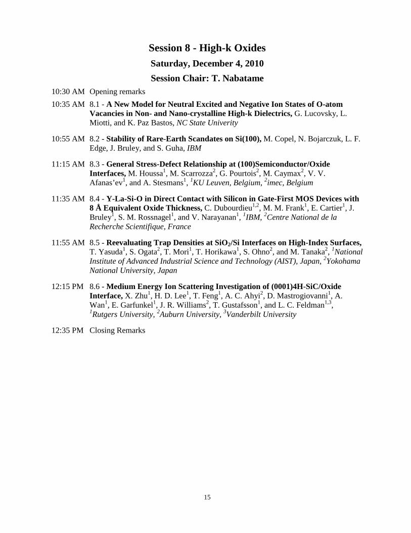
Session 8 - High-k Oxides Saturday, December 4, 2010 Session Chair: T. Nabatame
10:30 AM Opening remarks 10:35 AM 8.1 - A New Model for Neutral Excited and Negative Ion States of O-atom
Vacancies in Non- and Nano-crystalline High-k Dielectrics, G. Lucovsky, L. Miotti, and K. Paz Bastos, NC State Univerity
10:55 AM 8.2 - Stability of Rare-Earth Scandates on Si(100), M. Copel, N. Bojarczuk, L. F. Edge, J. Bruley, and S. Guha, IBM
11:15 AM 8.3 - General Stress-Defect Relationship at (100)Semiconductor/Oxide Interfaces, M. Houssa1, M. Scarrozza2, G. Pourtois2, M. Caymax2, V. V. Afanas’ev1, and A. Stesmans1, 1KU Leuven, Belgium, 2imec, Belgium
11:35 AM 8.4 - Y-La-Si-O in Direct Contact with Silicon in Gate-First MOS Devices with 8 Å Equivalent Oxide Thickness, C. Dubourdieu1,2, M. M. Frank1, E. Cartier1, J. Bruley1, S. M. Rossnagel1, and V. Narayanan1, 1IBM, 2Centre National de la Recherche Scientifique, France
11:55 AM 8.5 - Reevaluating Trap Densities at SiO2/Si Interfaces on High-Index Surfaces, T. Yasuda1, S. Ogata2, T. Mori1, T. Horikawa1, S. Ohno2, and M. Tanaka2, 1National Institute of Advanced Industrial Science and Technology (AIST), Japan, 2Yokohama National University, Japan
12:15 PM 8.6 - Medium Energy Ion Scattering Investigation of (0001)4H-SiC/Oxide Interface, X. Zhu1, H. D. Lee1, T. Feng1, A. C. Ahyi2, D. Mastrogiovanni1, A. Wan1, E. Garfunkel1, J. R. Williams2, T. Gustafsson1, and L. C. Feldman1,3, 1Rutgers University, 2Auburn University, 3Vanderbilt University
12:35 PM Closing Remarks
16
41st IEEE
Semiconductor Interface Specialists Conference
December 2-4, 2010 (Tutorial: Dec 1) The Catamaran Hotel, San Diego, CA
www.ieeesisc.org
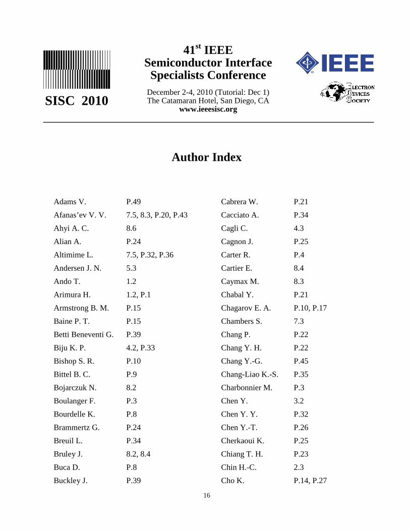
Author Index
Adams V. P.49
Afanas’ev V. V. 7.5, 8.3, P.20, P.43
Ahyi A. C. 8.6
Alian A. P.24
Altimime L. 7.5, P.32, P.36
Andersen J. N. 5.3
Ando T. 1.2
Arimura H. 1.2, P.1
Armstrong B. M. P.15
Baine P. T. P.15
Betti Beneventi G. P.39
Biju K. P. 4.2, P.33
Bishop S. R. P.10
Bittel B. C. P.9
Bojarczuk N. 8.2
Boulanger F. P.3
Bourdelle K. P.8
Brammertz G. P.24
Breuil L. P.34
Bruley J. 8.2, 8.4
Buca D. P.8
Buckley J. P.39
Cabrera W. P.21
Cacciato A. P.34
Cagli C. 4.3
Cagnon J. P.25
Carter R. P.4
Cartier E. 8.4
Caymax M. 8.3
Chabal Y. P.21
Chagarov E. A. P.10, P.17
Chambers S. 7.3
Chang P. P.22
Chang Y. H. P.22
Chang Y.-G. P.45
Chang-Liao K.-S. P.35
Charbonnier M. P.3
Chen Y. 3.2
Chen Y. Y. P.32
Chen Y.-T. P.26
Cherkaoui K. P.25
Chiang T. H. P.23
Chin H.-C. 2.3
Cho K. P.14, P.27
SISC 2010
17
Chu L. K. P.23
Chung Y. J. P.6
Clark S. J. 5.5
Clemens J. B. P.17
Cockburn A. P.34
Colombo L. P.28
Copel M. 1.2, 8.2
Coss B. E. P.5
Crupi F. P.42
Cui S. 1.3, P.31
Dao T. B. P.49
Date L. P.34
Davey W. P.7
De Meyer K. P.24
De Salvo B. P.39
Debusschere I. 7.5, P.34, P.36
Degraeve R. P.32, P.44
Dekkers H. P.34
Demkov A. A. 7.4
Detavernier C. P.36
Dhar S. P.48
Dong L. 7.2
Droopad R. P.17
Dubourdieu C. 8.4
Edge L. F. 8.2
Eizenberg M. P.9, P.31
Elshocht S. V. P.36
Eneman G. P.42
Everaert J. L. P.34
Fantini A. P.39
Feldman L. C. 8.6
Feng T. 7.3, 8.6
Fian A. 5.3
Fischetti M. V. 2.2
Fleetwood D. M. P.48
Franco J. P.42, P.44
Frank M. M. 8.4
Fraschke M. P.38
Fujii S. P.30
Fujiki J. P.30
Fukuhara N. 5.2, P.16
Gajula D. R. P.15
Garfunkel E. 7.3, 8.6
Ghibaudo G. P.3
Gong X. 2.3, P.46
Gordon R. G. 7.2
Goux L. P.32
Govoreanu B. P.32
Grampeix H. P.3, P.39
Grasser T. P.42, P.44
Groeseneken G. P.32, P.42, P.44
Guha S. 8.2
Guo P. P.41, P.46
Guo Y. 5.5
Gustafsson T. 7.3, 8.6
Haight R. 1.2
Hall S. P.7
Han G. P.41, P.46
Harries J. P.2
Hartmann J.-M. P.8
Hata M. 5.2, P.16
Hegde G. P.29
Heyns M. P.24
Hideshima I. 6.5, P.2
Higashi Y. P.30
Hinkle C. L. 5.1, P.18
Hjort M. 5.3
Hoffmann T. Y. P.24, P.42
18
Holland M. P.17
Hong M. P.22, P.23
Horikawa T. 8.5
Hoshii T. P.16
Hosoi T. 6.5, P.1, P.2, P.47
Houssa M. 8.3
Huang M. L. P.22, P.23
Hurley P. K. P.20, P.25
Hwang C. S. P.6
Hwang H. 4.2, P.33
Ielmini D. 4.3
Iida R. P.16
Im S. P.45
Ishii H. 5.2
Itatani T. 5.2
Iwasaki T. 6.3
Jammy R. P.5
Jo M. 4.2
Jo M. S. P.33
Jousseaume V. P.39
Jung H.-S. P.6
Jung S. 4.2
Jurczak M. P.32, P.34
Kaczer B. 7.5, P.36, P.42, P.44
Kagei Y. P.47
Kamata Y. 6.2
Kamimuta Y. 6.2
Kamiya K. 4.4
Kar G. S. P.34
Kasuya A. 6.5, P.2
Kauerauf T. P.44
Kaufman-Osborn T. P.10
Kelwing T. P.4
Keng W.-C. P.35
Keunen K. P.43
Kim D.-H. P.45
Kim H. K. P.6
Kim I. S. P.33
Kim J. 5.4, P.5, P.28
Kim M. S. 7.5, P.36
Kim S. 4.2
Kim S. H. P.16
Kim W.-H. P.6
Kirino T. P.47
Kirk A. P. 5.4
Kirsch P. 1.1
Kita K. 6.1, 6.4, P.11, P.12
Kitano N. P.1
Kittl J. A. 7.5, P.36
Klimeck G. P.29
Ko G. P.45
Kornblum L. P.31
Kummel A. C. P.10, P.17
Kusai H. P.30
Kutsuki K. 6.5, P.2
Kwo J. P.22, P.23
Le M. P.34
Lee B. P.28
Lee C. H. 6.4, P.12
Lee D. S. P.33
Lee H. D. 7.3, 8.6
Lee J. 3.2, 4.2, 7.4
Lee J. C. P.26
Lee J. S. P.10
Lee J.-M. P.33
Lee K. P.45
Lee N.-I. P.6
Lee S. P.16
19
Lee S. Y. P.6
Lee W. 4.2, P.34
Lee W. C. P.23
Lenahan P. M. P.9
Leroux C. P.3
Lin C. A. P.22
Lin D. P.20
Lin L. 5.5, P.13, P.14
Lin T. D. P.23
Lind E. 5.3
Lipp E. P.9
Liu L.-J. P.35
Liu X. P.40
Liu Y. Q. 7.2
Liu Z. 1.3
Loh W.-Y. P.5
Long R. D. P.25
Lopes J. M. J. P.7, P.8
Lorenzi P. P.39
Low Y. H. P.15
Lucovsky G. 8.1
Lukosius M. P.38
Ma T. P. P.31
Ma T.P. 1.3
Maeda T. 5.2
Majhi P. P.5
Mannhart J. 7.1
Mantl S. P.8
Martin F. P.3
Mastrogiovanni D. 8.6
McDonnell S. 5.4, P.28
McIntyre P. C. P.25
McNeill D. W. P.15
Merckling C. P.24
Meuris M. P.24
Mikkelsen A. 5.3
Miotti L. 8.1
Miranda E. P.38
Mitani S. P.47
Mitard J. P.42
Mitrovic I. Z. P.7
Miyata N. 5.2, P.16
Modreanu M. P.15
Monaghan S. P.25
Mori T. 8.5
Muraoka K. P.30
Nadimi E. P.4
Nagashio K. 6.4, P.11
Nakamura T. P.47
Nakano Y. P.47
Narayanan V. 1.2, 8.4
Nardi F. 4.3
Nemanich R. J. P.40
Newcomb S. B. P.20
Nichau A. P.8
Nishimura T. 6.4, P.11, P.12
Nitayama A. 4.1
Nodin J. F. P.39
O'Regan T. 2.2
Ogata S. 8.5
Ohno S. 8.5
Okamoto G. P.2
Opsomer K. P.36
Otake A. 4.4
Öttking R. P.4
Pantisano L. P.32
Park J. 4.2
Park J. B. P.33
20
Park J.-M. P.6
Park S. 4.2
Pawlak M. A. 7.5, P.36
Paz Bastos K. 8.1
Perniola L. P.39
Persico A. P.39
Pi T.-W. P.22, P.23
Pirkle A. P.28
Plänitz P. P.4
Popovici M. I. 7.5, P.36
Pourtois G. 8.3
Radehaus C. P.4
Radosavljevic M. 2.1
Reimbold G. P.3
Rha S.-H. P.6
Rispal L. P.37
Robertson J. 5.5, P.13, P.14
Rossnagel S. M. 8.4
Roussel Ph. J. P.42, P.44
Ryu S.-H. P.48
Saeki M. P.1
Scarrozza M. 8.3
Schoofs G. P.34
Schrimpf R. D. P.48
Schroeder T. P.38
Schubert J. P.7, P.8
Schwalke U. P.37
Sedghi N. P.7
Seo K. A. P.33
Shen J. P.17
Shi X. P.34
Shigeta Y. 4.4
Shimura T. 6.5, P.1, P.2, P.47
Shin B. P.25
Shin J. 4.2
Shin J. H. P.33
Shiraishi K. 4.4
Siddik M. P.33
Singh P. P.39
Song M.-W. P.6
Sonnet A. M. P.18
Stemmer S. P.25
Stesmans A. 8.3, P.20, P.43
Strachan A. P.29
Sun X. P.31
Suzuki R. P.16
Swerts J. P.36
Tabata T. P.12
Takagi S. 5.2, 6.3, P.16
Takenaka M. 5.2, 6.3, P.16
Tanaka M. 8.5
Tang F. P.40
Tantraviwat D. P.15
Taoka N. 5.2, 6.3, P.16
Teraoka Y. P.2, P.47
Tezuka T. 6.2
Thelander C. 5.3
Tillack B. P.38
Timm R. 5.3
Tirano S. P.39
Toledano-Luque M. P.44
Tomida K. 7.5, P.36
Toriumi A. 6.4, P.11, P.12
Trentzsch M. P.4
Triyoso D. H. P.49
Urabe Y. 5.2, P.16
Van den Bosch G. P.34
Van Elshocht S. 7.5
21
Van Houdt J. P.34
Vogel E. M. P.18
Vrancken C. P.36
Walczyk Ch. P.38
Walczyk D. P.38
Wallace R. M. 5.4, P.5, P.27, P.28
Wan A. 8.6
Wang S. K. P.11
Wang T.-K. P.35
Wang W. P.27
Wang W. C. 7.5
Wang X. P.8
Wang X. P. P.32
Wang Y. 3.2, P.26
Wang Y. C. P.23
Watanabe H. 1.2, 6.5, P.1, P.2, P.47
Wenger Ch. P.38
Wernersson L.-E. 5.3
Williams J. R. 8.6
Witters L. P.42
Wouters D. J. P.32
Xa L.-Q. P.34
Xiong K. P.13, P.14
Xu M. 7.2, P.19
Xue F. 3.2, P.26
Yamada H. 5.2, P.16
Yamaguchi K. 4.4
Yang J. P.31
Yang Y. P.41, P.46
Yasuda N. P.30
Yasuda T. 5.2, 8.5, P.16
Ye P. D. 7.2, P.19
Ye Z.-H. P.35
Yeo Y.-C. 2.3, 3.1, P.41, P.46
Yokoyama M. 5.2, P.16
Yoshida M. 6.4
Yoshigoe A. P.2, P.47
Yu W. P.8
Zahid M. P.34
Zhan C. P.41, P.46
Zhang B. P.8
Zhang C. X. P.48
Zhang E. X. P.48
Zhang R. 6.3
Zhang Y. 2.2
Zhao H. 3.2, P.26
Zhao Q. T. P.8
Zhernokletov D. M. 5.4
Zhou F. 3.2, P.26
Zhou Q. P.41
Zhu C. P.40
Zhu X. 8.6
Zhu Z. 2.3
22
41st IEEE
Semiconductor Interface Specialists Conference
December 2-4, 2010 (Tutorial: Dec 1) The Catamaran Hotel, San Diego, CA
www.ieeesisc.org
Affiliation Index
Applied Materials P.34
Arizona State University P.40
Auburn University 8.6
CEA-LETI-MINATEC, France P.3, P.8, P.39
Centre National de la Recherche Scientifique, France 8.4
Chinese Academy of Sciences, China P.8
Cree P.48
Durham University, UK 5.5
Freescale Semiconductor P.49
FWO Vlaanderen, Belgium P.42
Ghent University, Belgium P.36
Glebe Scientific Ltd., Ireland P.20
Global Foundries, Germany P.4
Gwangju Institute of Science and Technology, Korea 4.2, P.33
GWT–TUD GmbH, Germany P.4
Harvard University 7.2
IBM 1.2, 8.2, 8.4
IHP, Germany P.38
imec, Belgium 7.5, 8.3, P.20, P.24, P.32, P.34, P.36, P.42, P.44
SISC 2010
23
IMEP Minatec, France P.3
Intel 2.1
Japan Atomic Energy Agency, Japan P.2, P.47
JST-CREST, Japan 6.4, P.11, P.12
KU Leuven, Belgium 7.5, 8.3, P.20, P.24, P.32, P.42, P.43, P.44
LG Display, Korea P.45
Lund University, Sweden 5.3
MIRAI-Toshiba, Japan 6.2
National Institute of Advanced Industrial Science and Technology (AIST), Japan
5.2, 8.5, P.16
National Synchrotron Radiation Research Center, Taiwan
P.22, P.23
National Tsing Hua University, Taiwan P.22, P.23, P.35
National University of Singapore, Singapore 2.3, 3.1, P.41, P.46
NC State Univerity 8.1
Osaka University, Japan 1.2, 6.5, P.1, P.2, P.47
Pacific Northwest National Laboratory 7.3
Politecnico di Milano, Italy 4.3
Purdue University 7.2, P.19, P.29
Queen’s University Belfast, UK P.15
Research Centre Jülich, Germany P.7, P.8
Rohm Co., Japan P.47
Rutgers University 7.3, 8.6
Samsung, Korea P.6
SEMATECH 1.1, P.5
Seoul National University, Korea P.6
SOITEC, France P.8
Stanford University P.25
Sumitomo Chemical Co., Japan 5.2, P.16
Technion-Israel Institute of Technology, Israel P.9, P.31
24
Technische Universität Chemnitz, Germany P.4
Technische Universität Darmstadt, Germany P.37
Texas Instruments P.28
Texas State University-San Marcos P.17
The Pennsylvania State University P.9
The University of Tokyo, Japan 5.2, 6.1, 6.3, 6.4, P.11, P.12, P.16
Toshiba, Japan 4.1, P.30
TU Wien, Austria P.42, P.44
Tyndall National Institute, Ireland P.15, P.20, P.25
UC San Diego P.10, P.17
UC Santa Barbara P.25
Universidad Complutense de Madrid, Spain P.44
Universitat Autònoma de Barcelona, Spain P.38
University of Augsburg, Germany 7.1
University of Cambridge, UK 5.5, P.13, P.14
University of Glasgow, UK P.17
University of Hyogo, Japan 4.4
University of Liverpool, UK P.7
University of Massachusetts Amherst 2.2
University of Tsukuba, Japan 4.4
Università della Calabria, Italy P.42
UT Austin 3.2, 7.4, P.26
UT Dallas 5.1, 5.4, P.5, P.13, P.14, P.18, P.21, P.27, P.28
Vanderbilt University 8.6, P.48
Yale University 1.3, P.31
Yokohama National University, Japan 8.5
Yonsei University, Korea P.45

25


![[41st KUG PP] Keynote & PowerPoint](https://static.fdocuments.in/doc/165x107/54b892024a795978368b45ac/41st-kug-pp-keynote-powerpoint.jpg)