4: Delay Basics - Indian Institute of Science
13
4: Delay Basics
Transcript of 4: Delay Basics - Indian Institute of Science

4: Delay Basics

arrival time, max, slack, positive slack, negative slack

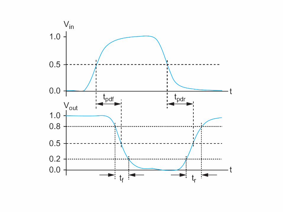
Vi V
o
CL
1.01cm
I
Tpdf
Sir
Sof
CLdV odt
=−I
∫0
T
dt=∫VDD
0 CLIdV o
CL=CL V o , V i , S ir , Sof I=I V o , V i
Choose sizes for PMOS and NMOS such that Rr = R
f
Vi V
o
CL
1.01cm
I
Tpdf
Sir
Sof
T pdf= f S ir ,CL ,W /L n ,W /L pS of=gS ir ,CL , W /L n ,W /L p
When S ix≈S oxT pdf≈R f∗CLT pdr≈R r∗CL
choose R f≈R rby appropriate sizing
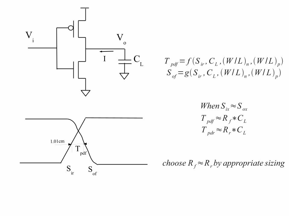
RC
d
Cs
Cg
Ideal switch
W/L
RC Model for Transistor
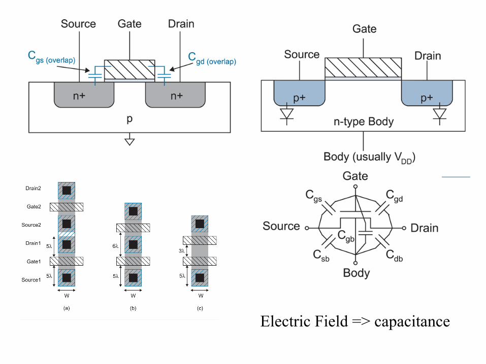
Electric Field => capacitance

Voltage dependantcapacitance
Nonlinear
C V =dQ
dV
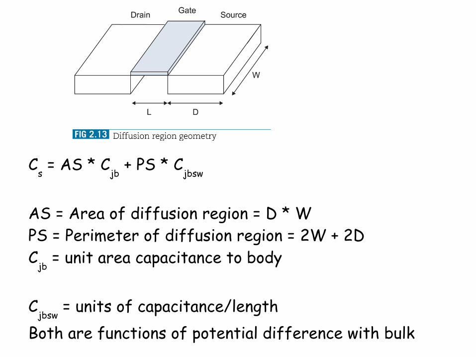
Cs = AS * C
jb + PS * C
jbsw
AS = Area of diffusion region = D * WPS = Perimeter of diffusion region = 2W + 2DC
jb = unit area capacitance to body
Cjbsw
= units of capacitance/lengthBoth are functions of potential difference with bulk

RC
d
Cs
Cg
Ideal switch
Cq ~ ε
ox * L /t
ox ~ 1.5-2 fF/um of width across technology
Similarly, C
d = K
d W, Since area drain is proportional to W
Cd ~ C
g
W/L
RC Model for Transistor
Cg=1V dd
∫0
Vdd
C inp v dv
C inp v ∝W⇒Cg=K g∗W