Substrate-embedded and flip-chip-bonded photodetector polymer-based optical interconnects

3D SiP with Embedded Chip ProvidingIntegration Solutions for Power Applications
Lee Smith3D-PEIMJune 14, 2016

Outline
Introduction of UTAC and System in a Package (SiP) Sites
Multi-chip Package (MCP) / SiP Forecast & Attributes
Trends & Applications, Trade offs for 3D SiP w/ Embedded Chip
Adoptions of Embedded Chip Packaging in Power and HighDensity Applications
3D SiP with Embedded Chip UTAC / AT&S Collaboration
Summary
1

2
UTAC at a Glance
• Outsourced Semiconductor Assembly and Test services (“OSAT”) provider insupport of Analog, Mixed-Signal, Logic, Power and Memory products.
• UTAC 2015 Revenue $878M; Ranked 6th in the Top Ten OSAT
• Focus – Assy, Test and Turnkey; Test comprises 35% in 2015.
• 1997 Established in Singapore
• HQ in Singapore; Mfg - Singapore, Taiwan, Malaysia, Indonesia, Thailand, China.
• >260K M2 Manufacturing Space and about 12K Employees Globally.
• Sales offices located worldwide.
• Markets: Mobile Phone, Automotive, Security, Wearable’s, Industrial & Medical.
2

UTAC Thailand (UTL)[Since 1973, 640k sq ft, Auto & Security certs.]QFN, GQFN, LGA, MIS MEMS, Cu Clip
UTAC SiP Sites Summary
UTAC Shanghai, China (USC)[90k sq ft, WGQ Free trade zone]QFN, FBGA, LGA, MIS
UTAC Dongguan, China (UDG)[Since 1988, >500k sq ft, China Logistics, WW distribution]BGA, LGA, QFN, Memory Cards, USB, SiP, 3D SiP w/Embedded chip
3
4
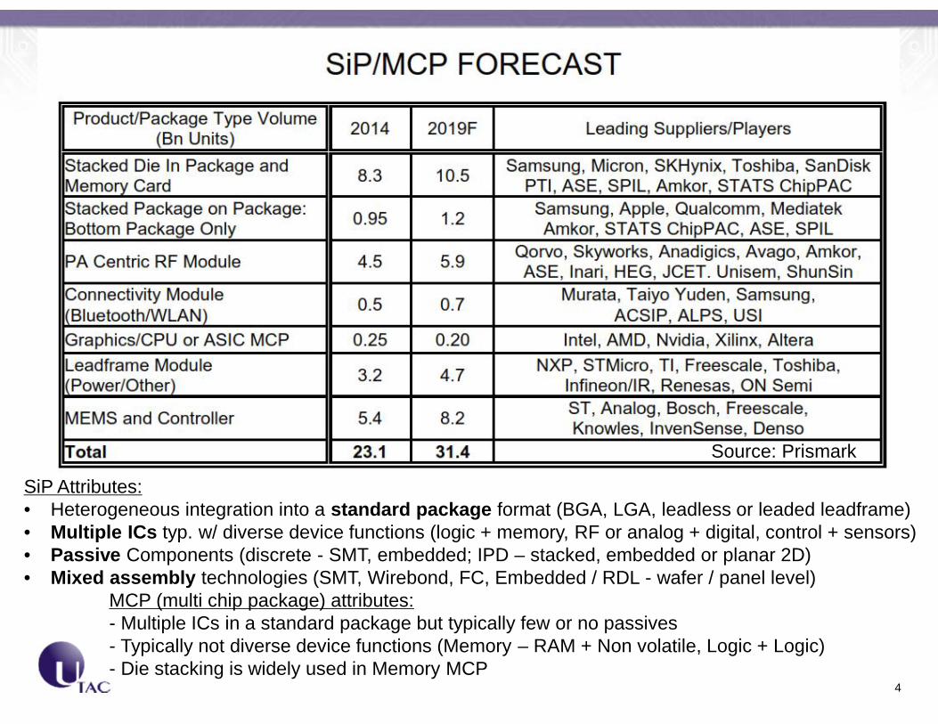
Source: Prismark
SiP Attributes:• Heterogeneous integration into a standard package format (BGA, LGA, leadless or leaded leadframe)• Multiple ICs typ. w/ diverse device functions (logic + memory, RF or analog + digital, control + sensors)• Passive Components (discrete - SMT, embedded; IPD – stacked, embedded or planar 2D)• Mixed assembly technologies (SMT, Wirebond, FC, Embedded / RDL - wafer / panel level)
MCP (multi chip package) attributes:- Multiple ICs in a standard package but typically few or no passives- Typically not diverse device functions (Memory – RAM + Non volatile, Logic + Logic)- Die stacking is widely used in Memory MCP

CMOS driver
CbypGaAs FET die
other passiveComponents SMT
Trend to 3D SiP with Embedded Chip
DieFETFET
R, L, C
5

Applications for 3D SiP with Embedded chip
6

3D SiP w/ Embedded Chip Pros / Cons
7
Miniaturization:+ Reduced SiP component footprint area- Increased SiP component mounted Z height
Design flexibility:+ Tailor the interconnect technology (embedded via, wirebond, FC or SMT)
Allows embedded chip technology to provide higher wiring density solutions.(Co-design methodology is required to optimize for system and devicecost / performance trade-offs. Chips first assembly techs require co-design for):- KGD requirements, design for test & yield optimization.
Electrical performance:+ Improved signal integrity or power efficiency thru shorter vertical (via)interconnects,power / ground planes in embedded chip substrates and lower package parasitics.+ EMI / RFI shielding and isolation of digital and RF devices thru ground planes andplated via ground fences along with ability to shield the top side assembly.+ 3D SiP architecture enables closer placement of critical passives(inductors, capacitors, filters, etc…) to IC devices.

Comparison of Package Area vs. Thermal Resistance
Source: GaNSystems,AT&SIMAPS 2014
8
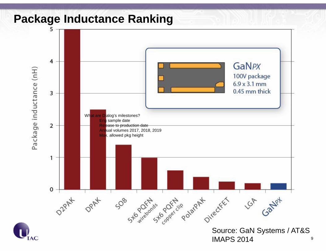
Package Inductance Ranking
Source: GaN Systems / AT&SIMAPS 2014 9
What are Dialog’s milestones?Eng sample dateRelease to production dateAnnual volumes 2017, 2018, 2019Max. allowed pkg height
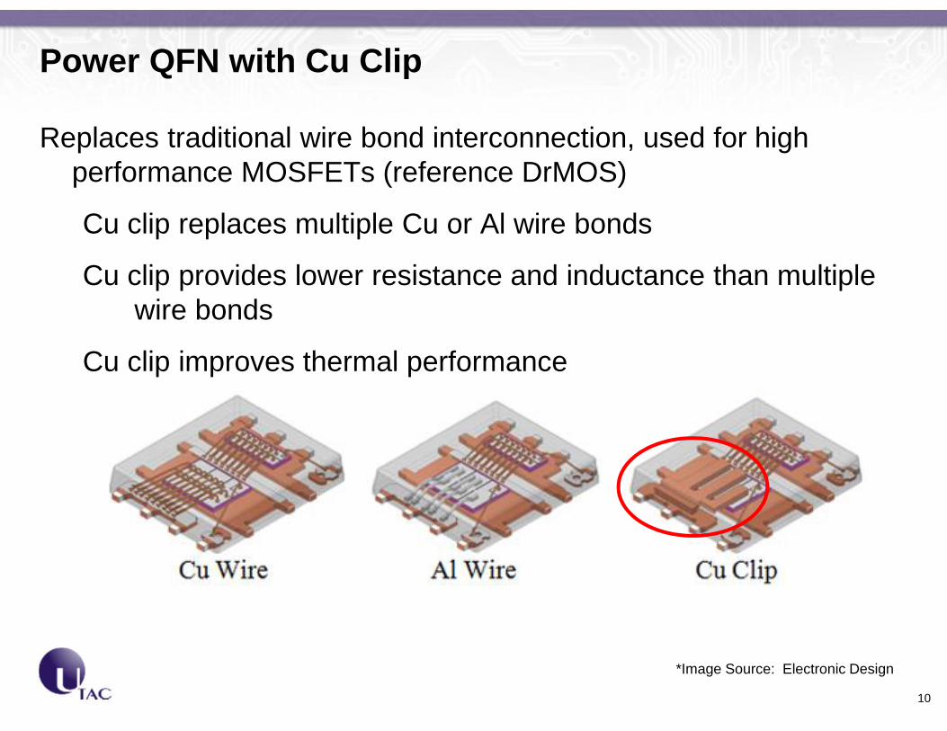
Power QFN with Cu Clip
Replaces traditional wire bond interconnection, used for highperformance MOSFETs (reference DrMOS)
Cu clip replaces multiple Cu or Al wire bonds
Cu clip provides lower resistance and inductance than multiplewire bonds
Cu clip improves thermal performance
10
*Image Source: Electronic Design

TI MicroSiP™ (Introduced 2011)> 20 products Step-down &Boost Converters
11
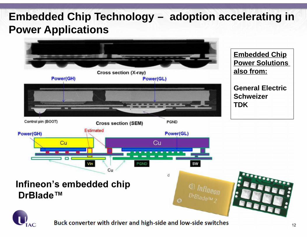
Infineon’s embedded chipDrBlade™
12
Embedded Chip Technology – adoption accelerating inPower Applications
Embedded ChipPower Solutionsalso from:
General ElectricSchweizerTDK

TDK’s SESUB Technology shrinks Power Managementsection 60% in BlackBerry™ Z10 Phone
13
14
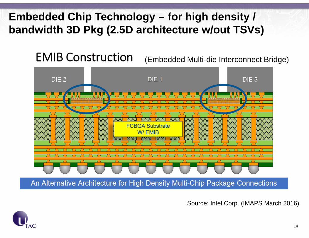
Embedded Chip Technology – for high density /bandwidth 3D Pkg (2.5D architecture w/out TSVs)
Source: Intel Corp. (IMAPS March 2016)
(Embedded Multi-die Interconnect Bridge)

Intel EMIB vs. 2.5D Silicon Interposer: Evaluation Matrix
Source: Intel Corp. R. Mahajan keynote IMAPS DPC 2016
15

Co-DesignCo-Design
Wafer toDie
Wafer toDie
Substrateembeddedchip
Substrateembeddedchip
PackageassemblyPackageassembly TestTest
SMTTop FC / under fill
Cap or MoldSolder Ball Attach
Package saw
KGD testRDL
Thin / DiceInspect / TnR
Substrate manufacturingEmbedded chip
Strip Test
Package level testReliability test
Alignment on DesignRules & Roadmaps- Substrate design- Assembly design
- Design integration
3D SiP Supply Chain UTAC / AT&S Collaboration
CustomerSpecs
CustomerConsignedOption
April 2015 - Joint marketing / supply chain agreementBetween AT&S and UTAC for 3D SiP with embedded chiptechnology. Collaboration press release April 2016.AT&S over 5 years production embedding experience.
16
CMOS driver
CbypGaAs FET die
other passiveComponents SMT

Laser-Drilling offiducials + overlay
Laser-Drilling offiducials + overlay
Component /DieAttach
Printing of adhesive
Attachment
Component /DieAttach
Printing of adhesive
Attachment
Layup & PressingLayup & Pressing
Laser DrillingLaser Drilling
Mechanical DrillingMechanical Drilling
DesmearingDesmearing
Metallization
Imaging
Copper Plating
Stripping + Etching
Metallization
Imaging
Copper Plating
Stripping + Etching
Auto-InspectionAuto-Inspection
Solder MaskSolder Mask
RoutingRouting
E-TestE-Test
Surface Finish(OSP/ENEPIG/NiPuAu)
Surface Finish(OSP/ENEPIG/NiPuAu)
Final InspectionFinal Inspection
SMT flowFC – U/F optional
Over mold orLid Attach
SMT flowFC – U/F optional
Over mold orLid Attach
Solder Ball AttachSolder Ball Attach
Packaging Level TestPackaging Level Test
* WLP Back-end
Back GrindWafer Saw
Inspect , KGD TestT&Reel
* WLP Back-end
Back GrindWafer Saw
Inspect , KGD TestT&Reel
Package SawPackage Saw
Visual InspectionVisual Inspection
AT&S
UDG* Die require 5-10um thick Cu pads for embedding at > 200um pad pitch
17
UTAC / AT&S 3D SiP Process Flow
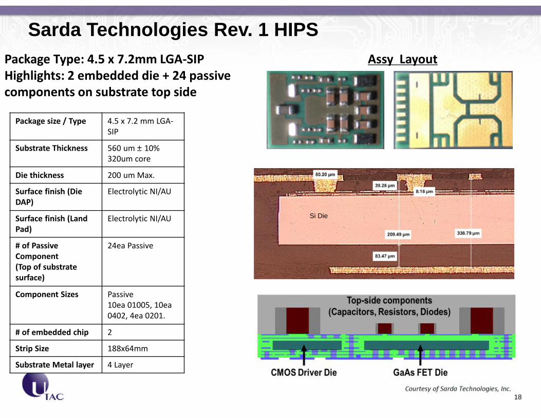
Package size / Type 4.5 x 7.2 mm LGA-SIP
Substrate Thickness 560 um ± 10%320um core
Die thickness 200 um Max.
Surface finish (DieDAP)
Electrolytic NI/AU
Surface finish (LandPad)
Electrolytic NI/AU
# of PassiveComponent(Top of substratesurface)
24ea Passive
Component Sizes Passive10ea 01005, 10ea0402, 4ea 0201.
# of embedded chip 2
Strip Size 188x64mm
Substrate Metal layer 4 Layer
Package Type: 4.5 x 7.2mm LGA-SIPHighlights: 2 embedded die + 24 passivecomponents on substrate top side
Assy Layout
Sarda Technologies Rev. 1 HIPS
Si Die
18

19
AT&S UDG LaminateRequirements
Method Specification Result Specification
Moisture Sensitivity Level Peak @ 260 C Minimum MSL3 MSL3
Thermal Cycling -55 C / +150 C 1000cycles passed (TC Grade 1) -55 C / +125 C ; 1000 cycles
HAST 110 C @ 85%RH @ 5VDC 264 hours passed uHAST - 130 C/85%RH; 96 hours
High TemperatureStorage @125 C 1000hours passed (TH Grade 2) 150 C ; 1000 hours
Temperature/ Humidity 85 C / 85%RH 1000hours passed (TH Group A) Per customer
Board bending 5mm/s 80K bends passed Per customer
Random vibration 3 g (rms) (5-500) Hz 30 min per axis passed Per customer
Shock 10kg @ 0.2ms 3 per direction passed Per customer
Reflow sensitivity Pb-free profile (255 C) 30 cycles passed Per customer
Drop Test 1500g @ 0.5ms 10 drops passed (MS Group F) Per customerUDG can perform ReliabilityTesting as required per CustomerSpecs.
AT&S Reliability Data and UDG Laminate Reliability Requirements3D SiP with Embedded Chip Reliability Summary
20
Summary
System in a package (SiP) is a strategic focus area for UTAC
3D SiP with Embedded Chip provides integration, size andperformance benefits over 2D planar SiP solutions
3D Embedded Chip technology adoption is accelerating inPower and High Density Interconnect Applications
Supply chain collaboration with AT&S for emerging 3D SiPsolutions with embedded chip technology will advanced thetechnology and provide FTK supply solution for customers