3D HETEROGNEOUS INTEGRATION: …autsys.aalto.fi/en/attach/MicroNanoRobotics/ICRA2013WS-Soussan.pdf3d...
50
3D HETEROGNEOUS INTEGRATION: CONVERGENCE BETWEEN DIE STACKING AND WAFER BONDING A FABRICATION PERSPECTIVE P.SOUSSAN MAY 10, 2013
-
Upload
phamkhuong -
Category
Documents
-
view
230 -
download
2
Transcript of 3D HETEROGNEOUS INTEGRATION: …autsys.aalto.fi/en/attach/MicroNanoRobotics/ICRA2013WS-Soussan.pdf3d...
3D HETEROGNEOUS INTEGRATION: CONVERGENCE BETWEEN DIE STACKING AND WAFER BONDING
A FABRICATION PERSPECTIVE
P.SOUSSAN
MAY 10, 2013
2
© IMEC 2013
OVERVIEW
▸ Introduction Semiconductors roadmap &
3D integrated products
▸ What is Heterogenous 3D integration
▸ Assembly techniques
▸ IMEC’s recent advances in heterogenous integration
research
▸ Conclusions
▸ Outlook
3
© IMEC 2013
OVERVIEW
▸ Introduction Semiconductors roadmap &
3D integrated products
▸ What is Heterogenous 3D integration
▸ Assembly techniques
▸ IMEC’s recent advances in heterogenous integration
research
▸ Conclusions
▸ Outlook
4
© IMEC 2013
SEMICONDUCTORS & MICROTECHNOLOGIES
2 FAMILIES
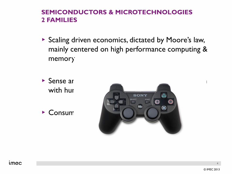
▸ Scaling driven economics, dictated by Moore’s law,
mainly centered on high performance computing &
memory
▸ Sense and interact, mainly centered on interaction
with humans & environment
▸ Consumers Vs specialty !!!
5
© IMEC 2013
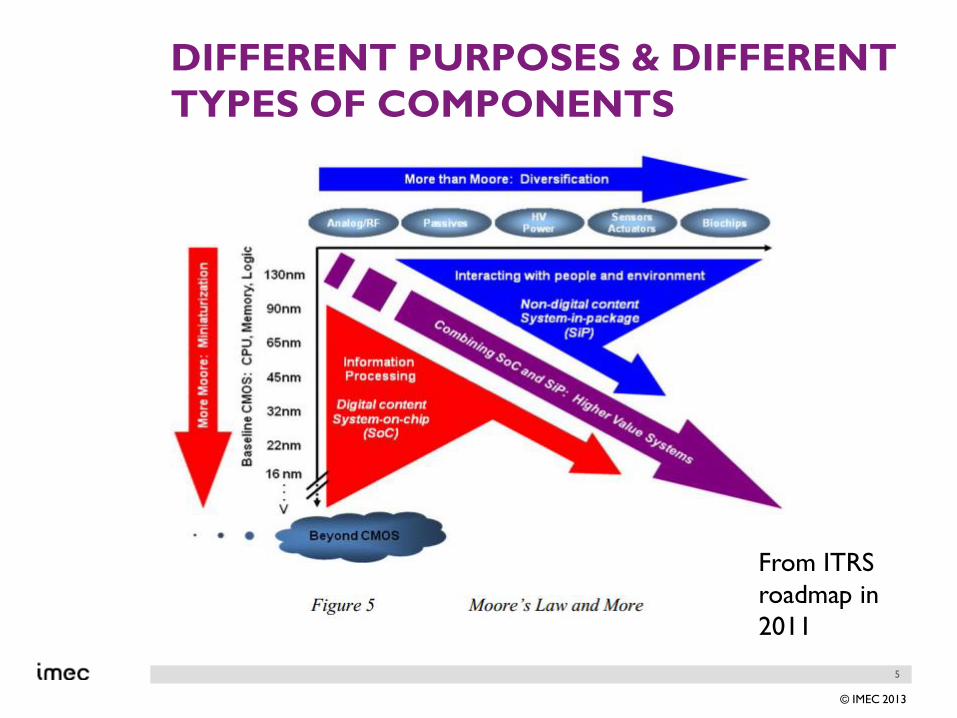
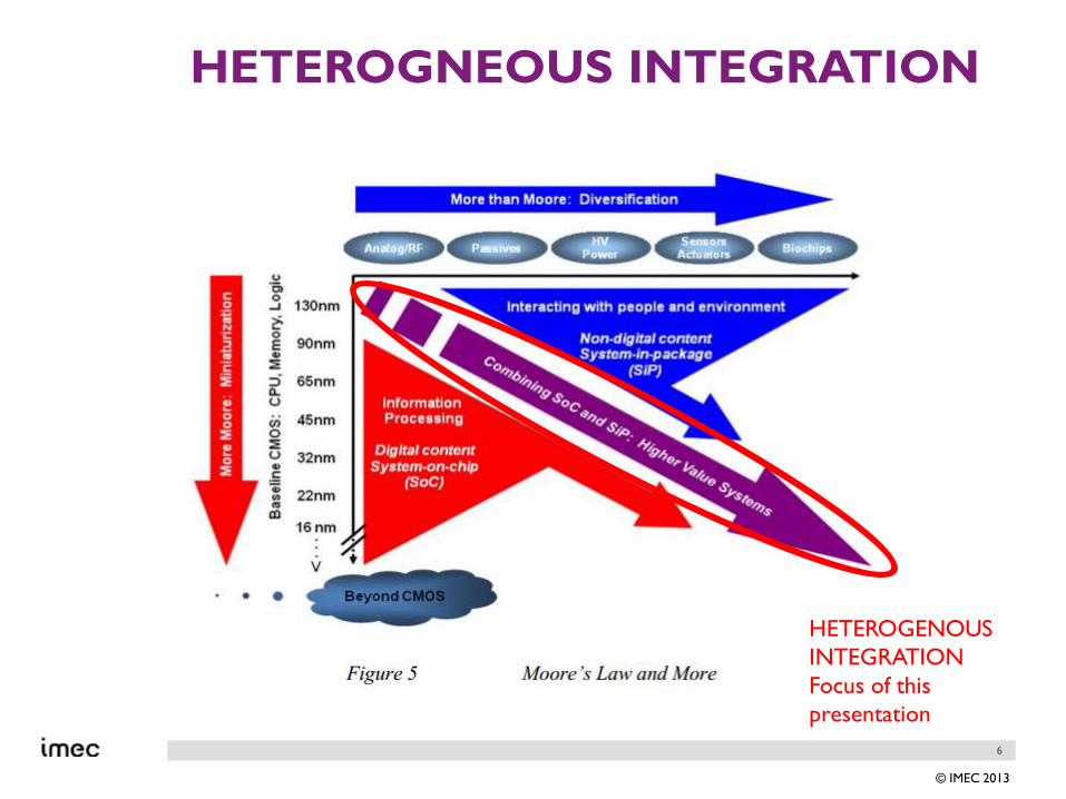
DIFFERENT PURPOSES & DIFFERENT
TYPES OF COMPONENTS
From ITRS
roadmap in
2011
6
© IMEC 2013
HETEROGNEOUS INTEGRATION
HETEROGENOUS
INTEGRATION
Focus of this
presentation
7
© IMEC 2013
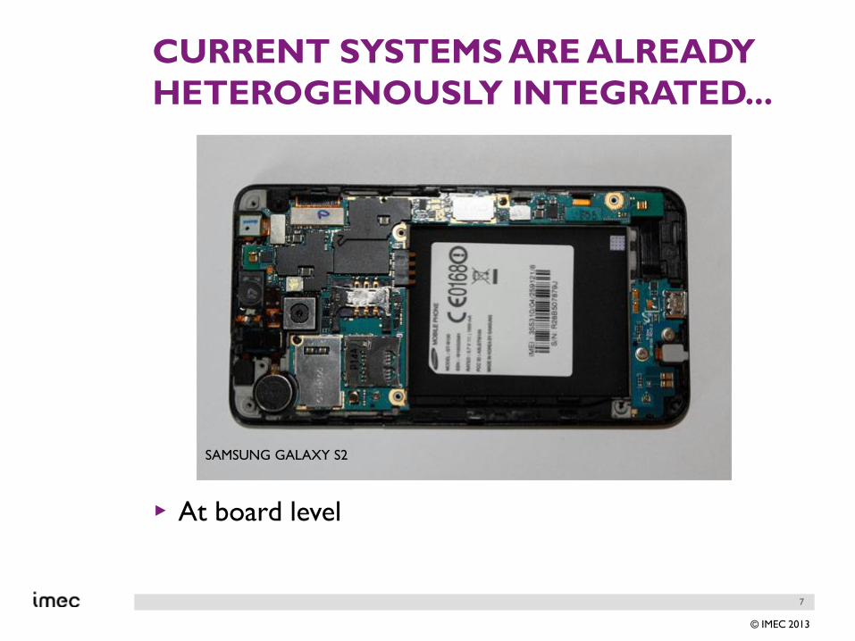
CURRENT SYSTEMS ARE ALREADY
HETEROGENOUSLY INTEGRATED...
▸ At board level
SAMSUNG GALAXY S2
8
© IMEC 2013
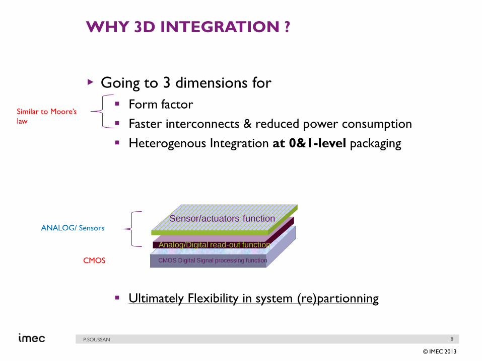
WHY 3D INTEGRATION ?
▸ Going to 3 dimensions for
Form factor
Faster interconnects & reduced power consumption
Heterogenous Integration at 0&1-level packaging
Ultimately Flexibility in system (re)partionning
P.SOUSSAN
Sensor/actuators function
CMOS Digital Signal processing function
Analog/Digital read-out function
Similar to Moore’s
law
CMOS
ANALOG/ Sensors
9
© IMEC 2013
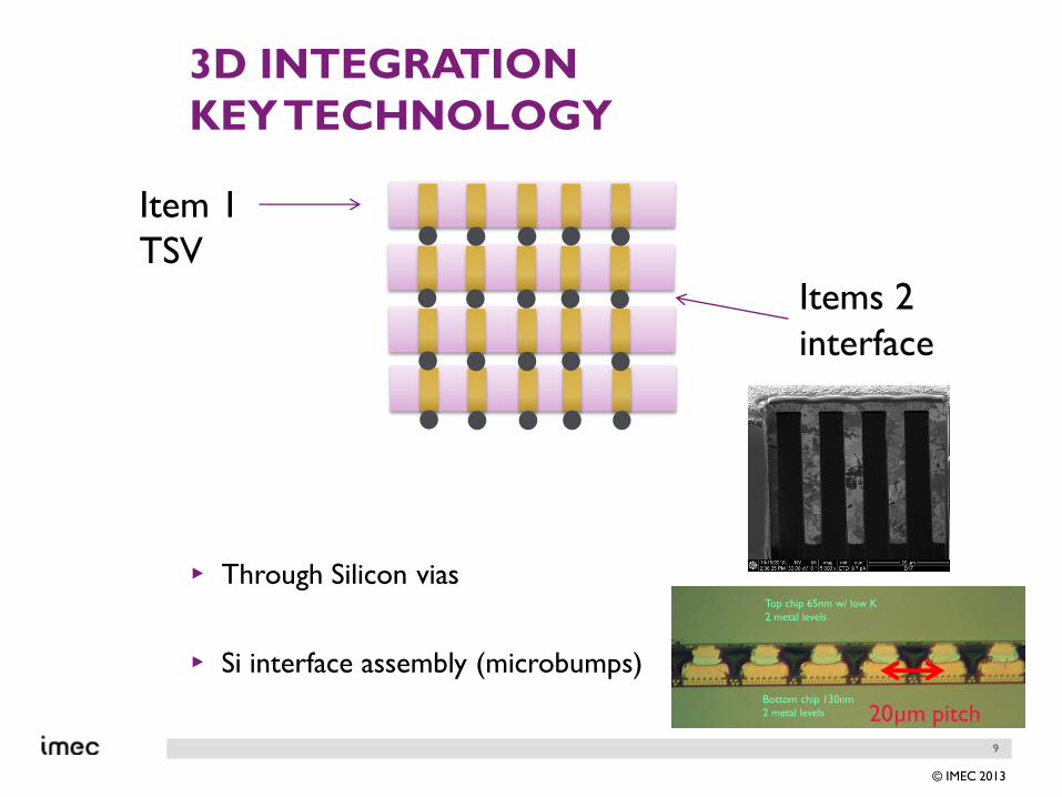
3D INTEGRATION
KEY TECHNOLOGY
▸ Through Silicon vias
▸ Si interface assembly (microbumps)
Item 1
TSV
Items 2
interface
Top chip 65nm w/ low K
2 metal levels
Bottom chip 130nm
2 metal levels 20µm pitch
10
© IMEC 2013
OVERVIEW
▸ Introduction Semiconductors roadmap &
3D integrated products
▸ What is Heterogenous 3D integration
▸ Assembly techniques
▸ IMEC’s recent advances in heterogenous integration
research
▸ Conclusions
▸ Outlook
11
© IMEC 2013
Short history of 3D integrated products
▸ Image sensors
▸ MEMS
▸ Interposers
12
© IMEC 2013
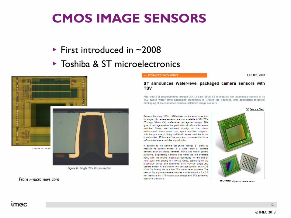
CMOS IMAGE SENSORS
▸ First introduced in ~2008
▸ Toshiba & ST microelectronics
From i-micronews.com
13
© IMEC 2013
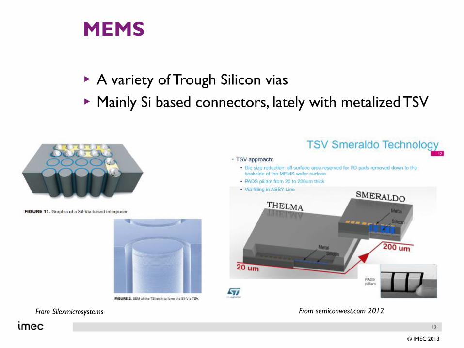
MEMS
▸ A variety of Trough Silicon vias
▸ Mainly Si based connectors, lately with metalized TSV
From semiconwest.com 2012From Silexmicrosystems
14
© IMEC 2013
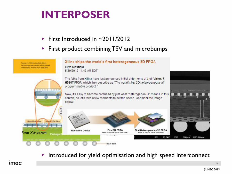
INTERPOSER
From Xilinks.com
▸ First Introduced in ~2011/2012
▸ First product combining TSV and microbumps
▸ Introduced for yield optimisation and high speed interconnect
15
© IMEC 2013
A FEW MORE WORDS ON
IMAGER SENSORS
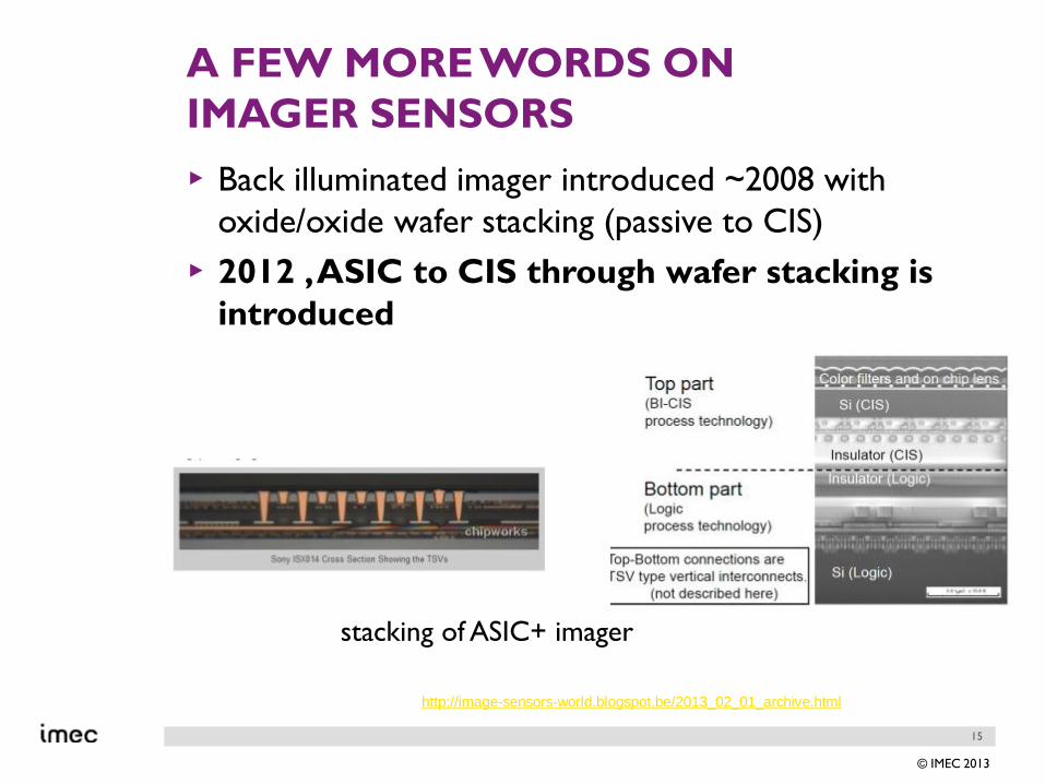
▸ Back illuminated imager introduced ~2008 with
oxide/oxide wafer stacking (passive to CIS)
▸ 2012 , ASIC to CIS through wafer stacking is
introduced
From chipworks.com
stacking of ASIC+ imager
http://image-sensors-world.blogspot.be/2013_02_01_archive.html
16
© IMEC 2013
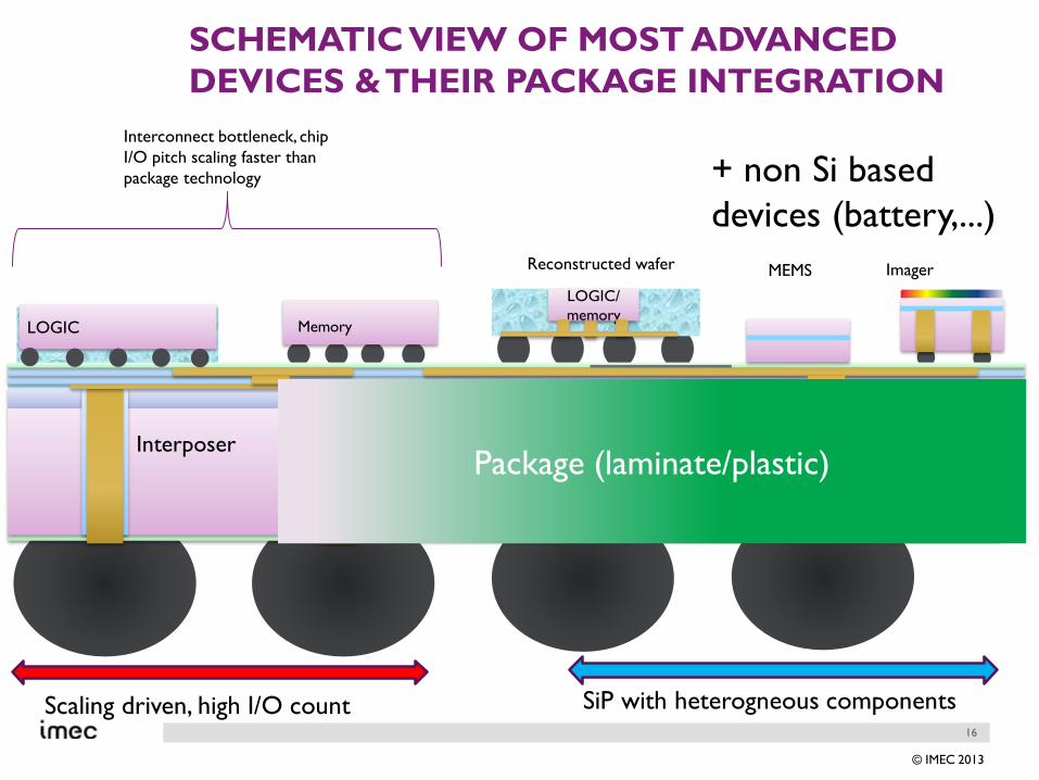
SCHEMATIC VIEW OF MOST ADVANCED
DEVICES & THEIR PACKAGE INTEGRATION
Interposer
ImagerMEMS
Package (laminate/plastic)
LOGIC/
memory
Reconstructed wafer
Scaling driven, high I/O count SiP with heterogneous components
Interconnect bottleneck, chip
I/O pitch scaling faster than
package technology
LOGIC Memory
+ non Si based
devices (battery,...)
17
© IMEC 2013
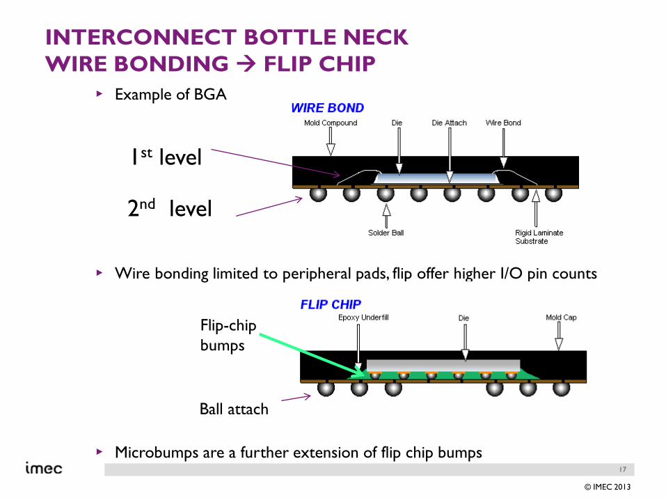
INTERCONNECT BOTTLE NECK
WIRE BONDING FLIP CHIP
▸ Example of BGA
▸ Wire bonding limited to peripheral pads, flip offer higher I/O pin counts
▸ Microbumps are a further extension of flip chip bumps
1st level
2nd level
Flip-chip
bumps
Ball attach
18
© IMEC 2013
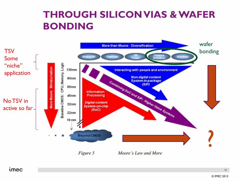
THROUGH SILICON VIAS & WAFER
BONDING
No TSV in
active so far
wafer
bondingTSV
Some
“niche”
application
?
19
© IMEC 2013
SUMMARY SEMICONDUCTORS & 3D INTEGRATION
FROM A FABRICATION PERSPECTIVE
Semiconductors & system integration
▸ System partionning occurs at PCB level = 3rd level packaging
▸ More Moore and More than Moore world still disconnected .
TSV
▸ The main driver is /was : replace wirebond for superior interconnect
performance and form factor
▸ No products (yet) relying on TSV + advanced CMOS nodes
▸ The volume of TSV’ed devices remain limited to lack of maturity of the TSV
manufacturing ,lack of standards, cost
Integration through ?
▸ Die level bonding is mainstream at 2nd level packaging
▸ Wafer stacking is a key enabling for device fabrication mainly for MEMS and
image sensors (0 level packaging)
What is Next ?
More system integration at lower hierarchical level... In which most
effective way ?
20
© IMEC 2013
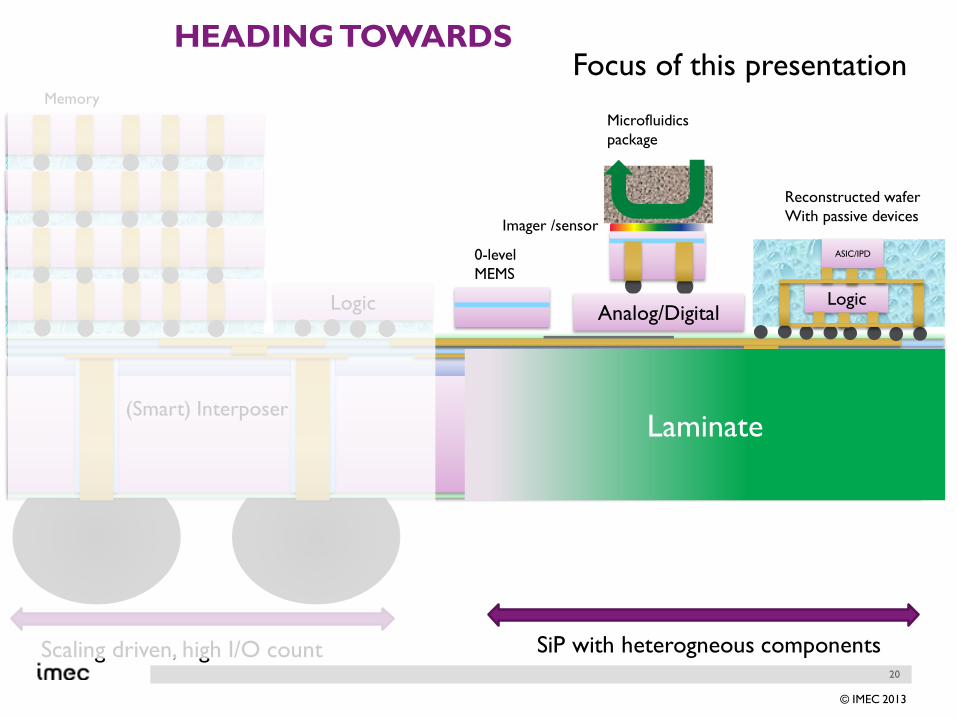
HEADING TOWARDS
Memory
Logic
(Smart) Interposer
Analog/Digital
Imager /sensor
0-level
MEMS
Laminate
Logic
ASIC/IPD
Reconstructed wafer
With passive devices
Microfluidics
package
Scaling driven, high I/O count SiP with heterogneous components
Focus of this presentation
21
© IMEC 2013
OVERVIEW
▸ Introduction Semiconductors roadmap &
3D integrated products
▸ What is Heterogenous 3D integration
▸ Assembly techniques
▸ IMEC’s recent advances in heterogenous integration
research
▸ Conclusions
▸ Outlook
22
© IMEC 2013
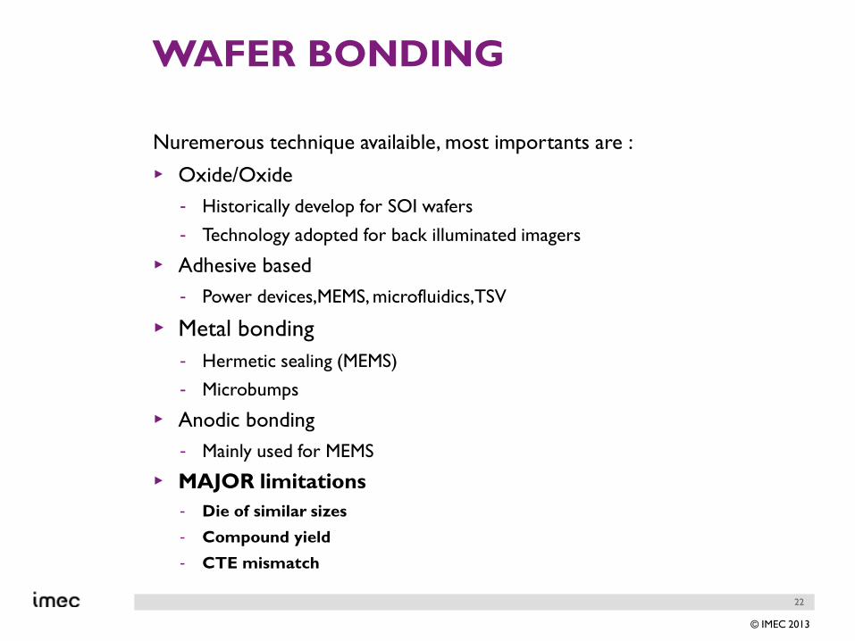
WAFER BONDING
Nuremerous technique availaible, most importants are :
▸ Oxide/Oxide
- Historically develop for SOI wafers
- Technology adopted for back illuminated imagers
▸ Adhesive based
- Power devices,MEMS, microfluidics, TSV
▸ Metal bonding
- Hermetic sealing (MEMS)
- Microbumps
▸ Anodic bonding
- Mainly used for MEMS
▸ MAJOR limitations
- Die of similar sizes
- Compound yield
- CTE mismatch
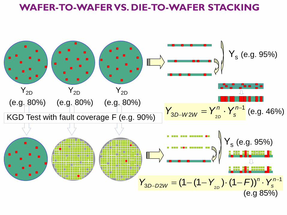
WAFER-TO-WAFER VS. DIE-TO-WAFER STACKING
1
23 2
n
s
n
WWD YYYD
(e.g. 46%)
Ys (e.g. 95%)
Y2D
(e.g. 80%)
Y2D
(e.g. 80%)
Y2D
(e.g. 80%)
KGD Test with fault coverage F (e.g. 90%)
Ys (e.g. 95%)
1
23 ))1()1(1(2
n
s
n
WDD YFYYD
(e.g 85%)
24
© IMEC 2013
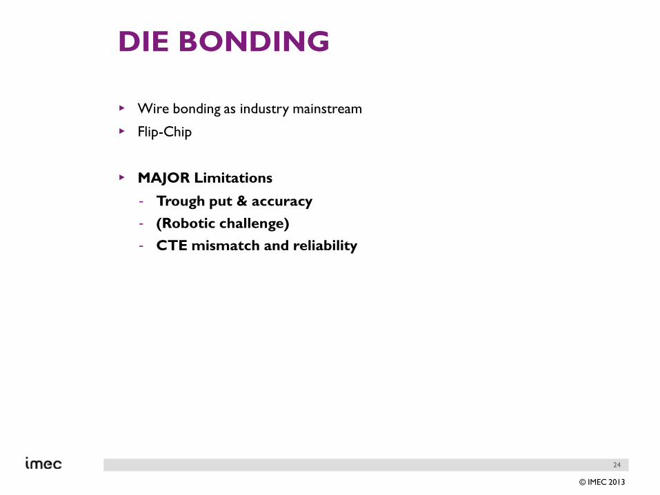
DIE BONDING
▸ Wire bonding as industry mainstream
▸ Flip-Chip
▸ MAJOR Limitations
- Trough put & accuracy
- (Robotic challenge)
- CTE mismatch and reliability
25
© IMEC 2013
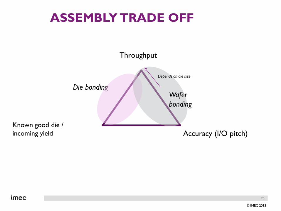
ASSEMBLY TRADE OFF
Throughput
Known good die /
incoming yield Accuracy (I/O pitch)
Die bondingWafer
bonding
Depends on die size
28
© IMEC 2013
OVERVIEW
▸ Introduction Semiconductors roadmap &
3D integrated products
▸ What is Heterogenous 3D integration
▸ Assembly techniques
▸ IMEC’s recent advances in heterogenous integration
research
▸ Conclusions
▸ Outlook
29
© IMEC 2013
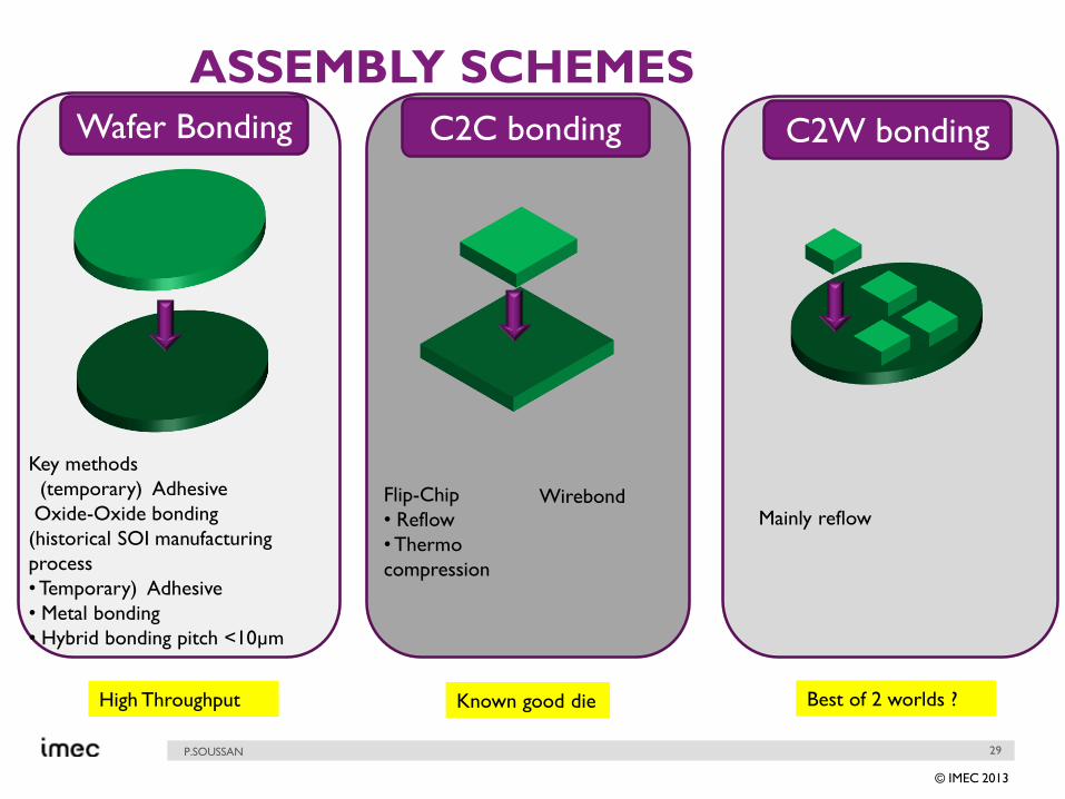
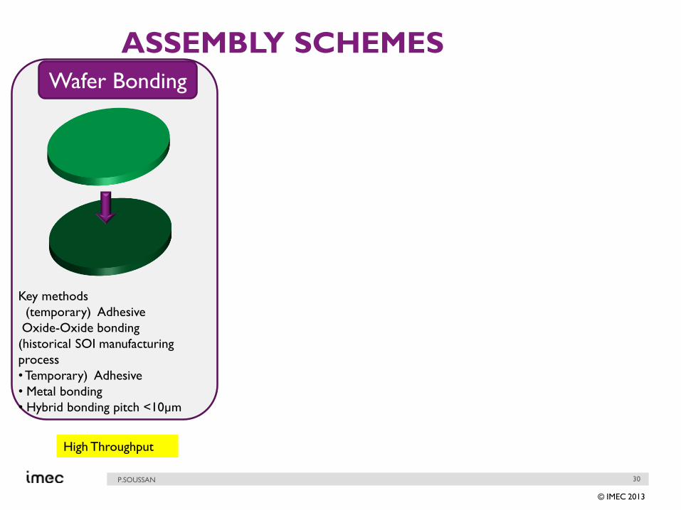
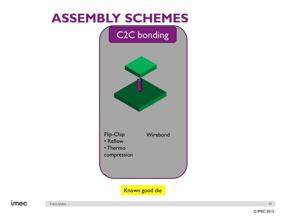
Best of 2 worlds ?
ASSEMBLY SCHEMES
P.SOUSSAN
Key methods
(temporary) Adhesive
Oxide-Oxide bonding
(historical SOI manufacturing
process
•Temporary) Adhesive
• Metal bonding
• Hybrid bonding pitch <10µm
Wafer Bonding
High Throughput Known good die
C2W bonding
Mainly reflowFlip-Chip
• Reflow
•Thermo
compression
C2C bonding
Wirebond
30
© IMEC 2013
ASSEMBLY SCHEMES
P.SOUSSAN
Key methods
(temporary) Adhesive
Oxide-Oxide bonding
(historical SOI manufacturing
process
•Temporary) Adhesive
• Metal bonding
• Hybrid bonding pitch <10µm
Wafer Bonding
High Throughput
31
© IMEC 2013
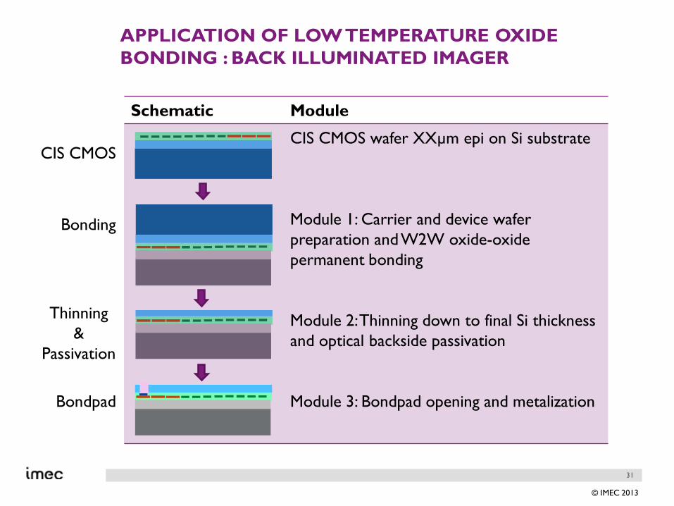
APPLICATION OF LOW TEMPERATURE OXIDE
BONDING : BACK ILLUMINATED IMAGER
Schematic Module
CIS CMOS wafer XXµm epi on Si substrate
Module 1: Carrier and device wafer
preparation and W2W oxide-oxide
permanent bonding
Module 2: Thinning down to final Si thickness
and optical backside passivation
Module 3: Bondpad opening and metalization
CIS CMOS
Bonding
Thinning
&
Passivation
Bondpad
32
© IMEC 2013
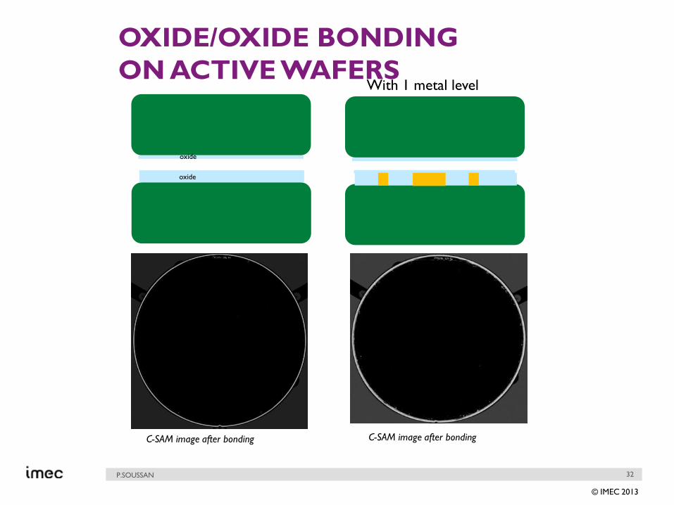
OXIDE/OXIDE BONDING
ON ACTIVE WAFERS
P.SOUSSAN
oxide
oxide
oxide
C-SAM image after bonding C-SAM image after bonding
With 1 metal level
33
© IMEC 2013
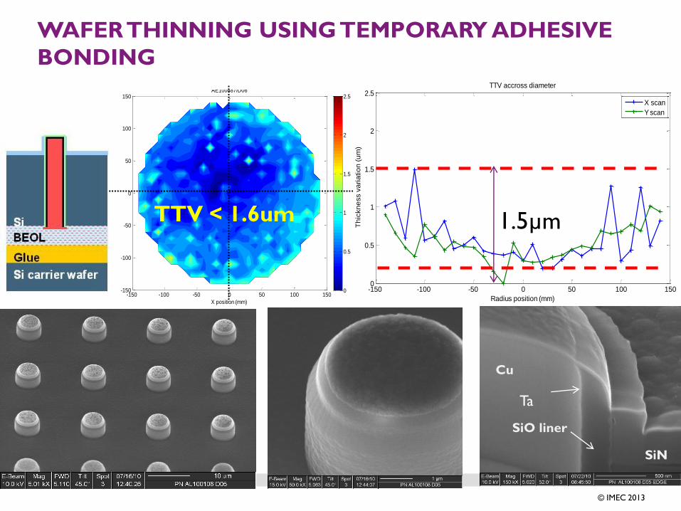
WAFER THINNING USING TEMPORARY ADHESIVE
BONDING
X position (mm)
Y p
ositio
n (
mm
)
Thickness variationAE100487/D06
-150 -100 -50 0 50 100 150-150
-100
-50
0
50
100
150
0
0.5
1
1.5
2
2.5
TTV < 1.6um
-150 -100 -50 0 50 100 1500
0.5
1
1.5
2
2.5
Radius position (mm)
Th
ickne
ss v
ari
atio
n (
um
)
TTV accross diameter
X scan
Y scan
1.5µm
SiO liner
SiN
Cu
Ta
34
© IMEC 2013
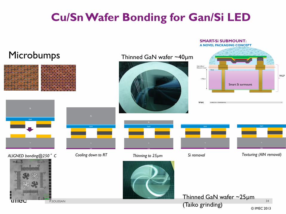
Cu/Sn Wafer Bonding for Gan/Si LED
P.SOUSSAN
Thinned GaN wafer ~40µm
GaN
Si
Si
SiN
GaN
Si
Si
SiN
GaN
Si
Si
SiN
GaN
Si
SiN
GaN
Si
SiN
ALIGNED bonding@250°C Cooling down to RT Thinning to 25µm Si removal Texturing (AlN removal)
Thinned GaN wafer ~25µm
(Taiko grinding)
© IMEC 2011 / CONFIDENTIAL
Oxide
~100µm
Hybrid Bond
Dielectric+metal
Smart Si surmount
WLP
17
SMART-Si SUBMOUNT: A NOVEL PACKAGING CONCEPT
Microbumps
35
© IMEC 2013
Oxide
Oxide
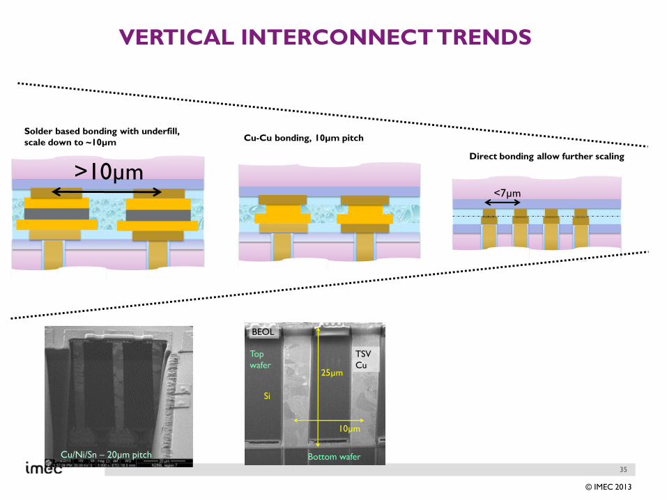
VERTICAL INTERCONNECT TRENDS
Cu/Ni/Sn – 20µm pitch
Solder based bonding with underfill,
scale down to ~10µm
>10µm
Top
wafer
Bottom wafer
TSV
Cu
Si
25µm
BEOL
10µm
<7µm
Direct bonding allow further scaling
Cu-Cu bonding, 10µm pitch
36
© IMEC 2013
ANODIC BONDING
▸ Bonding glass to Silicon with an hermetic seal
▸ Currently used for numerous MEMS applications
▸ High potential for Lab on Chip applications
37
© IMEC 2013
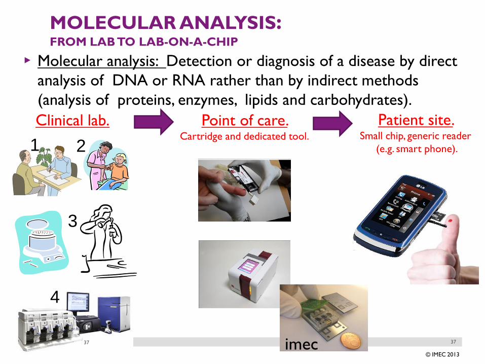
1 2
3
4
Clinical lab.
MOLECULAR ANALYSIS: FROM LAB TO LAB-ON-A-CHIP
37
Point of care. Cartridge and dedicated tool.
Patient site. Small chip, generic reader
(e.g. smart phone).
imec
▸ Molecular analysis: Detection or diagnosis of a disease by direct
analysis of DNA or RNA rather than by indirect methods
(analysis of proteins, enzymes, lipids and carbohydrates).
40
© IMEC 2013
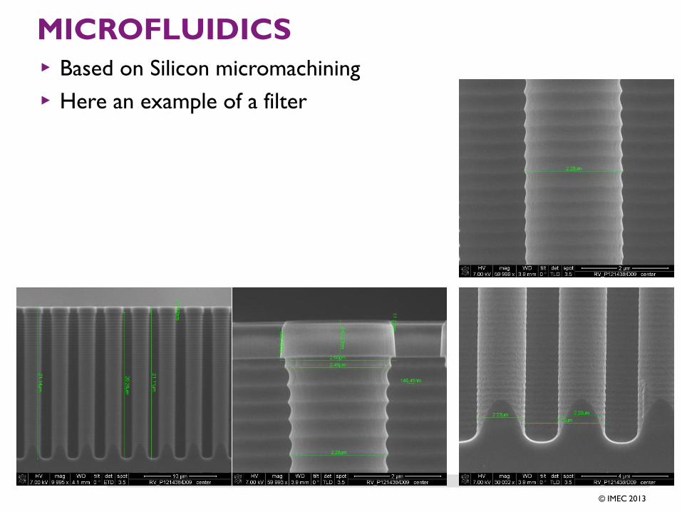
MICROFLUIDICS
▸ Based on Silicon micromachining
▸ Here an example of a filter
40
41
© IMEC 2013
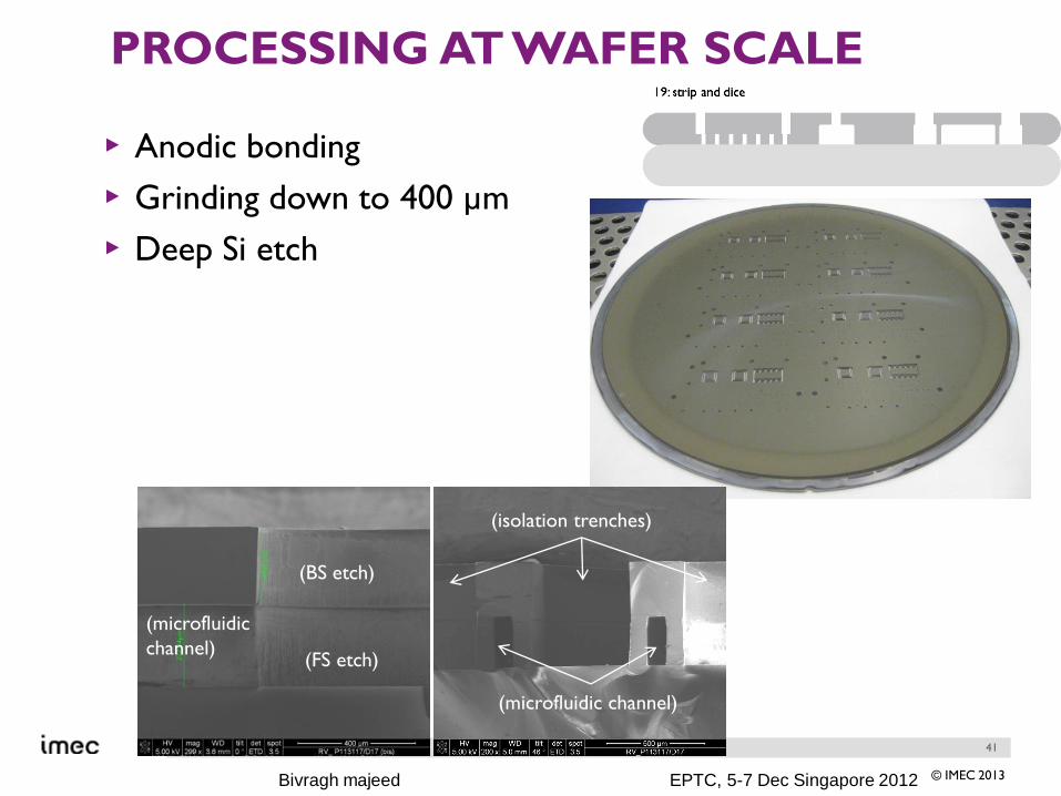
PROCESSING AT WAFER SCALE
▸ Anodic bonding
▸ Grinding down to 400 µm
▸ Deep Si etch
41
Bivragh majeed EPTC, 5-7 Dec Singapore 2012
(FS etch)
(isolation trenches)
(BS etch)
(microfluidic
channel)
(microfluidic channel)
42
© IMEC 2013
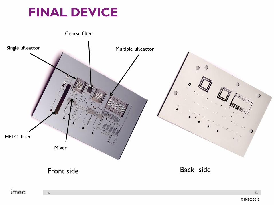
FINAL DEVICE
42
Front side Back side
Multiple uReactorSingle uReactor
Mixer
Coarse filter
HPLC filter
43
© IMEC 2013
ASSEMBLY SCHEMES
P.SOUSSAN
Known good die
Flip-Chip
• Reflow
•Thermo
compression
C2C bonding
Wirebond
44
© IMEC 2013
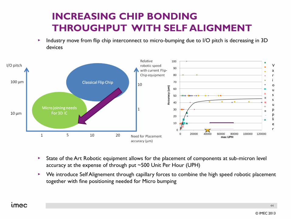
INCREASING CHIP BONDING
THROUGHPUT WITH SELF ALIGNMENT▸ Industry move from flip chip interconnect to micro-bumping due to I/O pitch is decreasing in 3D
devices
▸ State of the Art Robotic equipment allows for the placement of components at sub-micron level
accuracy at the expense of through put ~500 Unit Per Hour (UPH)
▸ We introduce Self Alignement through capillary forces to combine the high speed robotic placement
together with fine positioning needed for Micro bumping
Panasonic
Assembleon
Hesse & Knipps
0
10
20
30
40
50
60
70
80
90
100
0 20000 40000 60000 80000 100000 120000 max UPH
Ac
cu
rac
y (
um
)
Juki Siemens Samsung Samsung(2)
ASM Shibatec Oerlikon
Finetech TDK Semicorp Datacon
FAB2ASM
V
a
r
i
o
u
s
s
u
p
p
li
e
rTARGET
45
© IMEC 2013
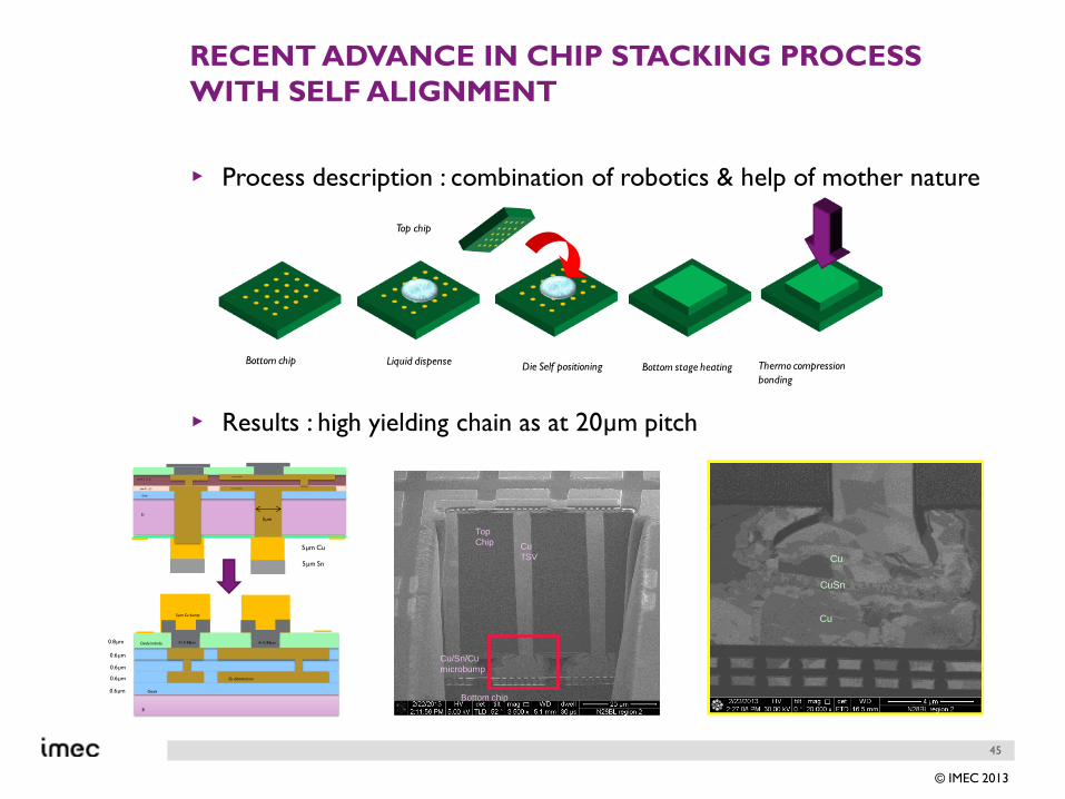
RECENT ADVANCE IN CHIP STACKING PROCESS
WITH SELF ALIGNMENT
▸ Process description : combination of robotics & help of mother nature
▸ Results : high yielding chain as at 20µm pitch
Top chip
Bottom chip Liquid dispenseDie Self positioning Bottom stage heating Thermo compression
bonding
Oxide
Cu si ngl e damascene
Si
Low K1 (3)
Low K2 (2.5)Cu dual damascene
5µm
5µm Cu
5µm Sn
Oxide
Cu damascene
0.8µm
0.6µm
0.6µm
0.6µm
0.6µm
Si
5µm Cu bump
Oxide/nitride Al 0.88µm Al 0.88µm
Cu
TSV
Top
Chip
Bottom chip
Cu/Sn/Cu
microbump
Cu
CuSn
Cu
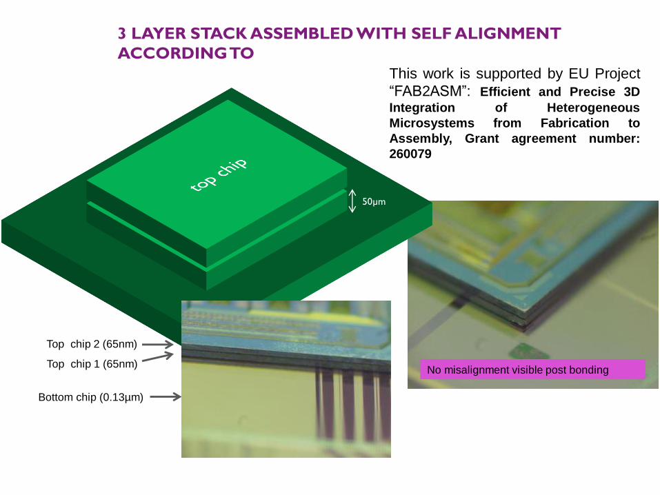
3 LAYER STACK ASSEMBLED WITH SELF ALIGNMENT
ACCORDING TO
Bottom chip (0.13µm)
Top chip 1 (65nm)
Top chip 2 (65nm)
No misalignment visible post bonding
50µm
This work is supported by EU Project
“FAB2ASM”: Efficient and Precise 3D
Integration of Heterogeneous
Microsystems from Fabrication to
Assembly, Grant agreement number:
260079
47
© IMEC 2013
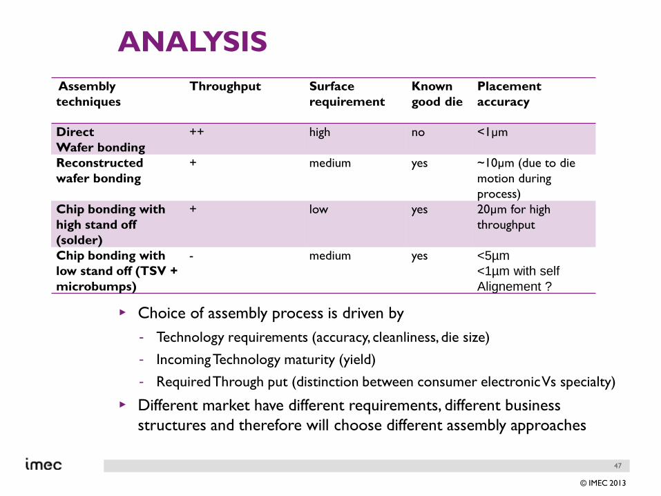
ANALYSIS
▸ Choice of assembly process is driven by
- Technology requirements (accuracy, cleanliness, die size)
- Incoming Technology maturity (yield)
- Required Through put (distinction between consumer electronic Vs specialty)
▸ Different market have different requirements, different business
structures and therefore will choose different assembly approaches
Assembly
techniques
Throughput Surface
requirement
Known
good die
Placement
accuracy
Direct
Wafer bonding
++ high no <1µm
Reconstructed
wafer bonding
+ medium yes ~10µm (due to die
motion during
process)
Chip bonding with
high stand off
(solder)
+ low yes 20µm for high
throughput
Chip bonding with
low stand off (TSV +
microbumps)
- medium yes <5µm
<1µm with self
Alignement ?
48
© IMEC 2013
OVERVIEW
▸ Introduction Semiconductors roadmap &
3D integrated products
▸ What is Heterogenous 3D integration
▸ Assembly techniques
▸ IMEC’s recent advances in heterogenous integration
research
▸ Conclusions
▸ Outlook
49
© IMEC 2013
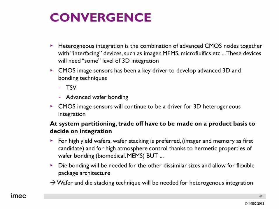
CONVERGENCE
▸ Heterogneous integration is the combination of advanced CMOS nodes together
with “interfacing” devices, such as imager, MEMS, microfluifics etc.... These devices
will need “some” level of 3D integration
▸ CMOS image sensors has been a key driver to develop advanced 3D and
bonding techniques
- TSV
- Advanced wafer bonding
▸ CMOS image sensors will continue to be a driver for 3D heterogeneous
integration
At system partitioning, trade off have to be made on a product basis to
decide on integration
▸ For high yield wafers, wafer stacking is preferred, (imager and memory as first
candidate) and for high atmosphere control thanks to hermetic properties of
wafer bonding (biomedical, MEMS) BUT ...
▸ Die bonding will be needed for the other dissimilar sizes and allow for flexible
package architecture
Wafer and die stacking technique will be needed for heterogenous integration
51
© IMEC 2013
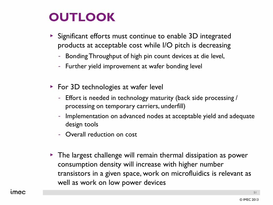
OUTLOOK
▸ Significant efforts must continue to enable 3D integrated
products at acceptable cost while I/O pitch is decreasing
- Bonding Throughput of high pin count devices at die level,
- Further yield improvement at wafer bonding level
▸ For 3D technologies at wafer level
- Effort is needed in technology maturity (back side processing /
processing on temporary carriers, underfill)
- Implementation on advanced nodes at acceptable yield and adequate
design tools
- Overall reduction on cost
▸ The largest challenge will remain thermal dissipation as power
consumption density will increase with higher number
transistors in a given space, work on microfluidics is relevant as
well as work on low power devices
52
© IMEC 2013
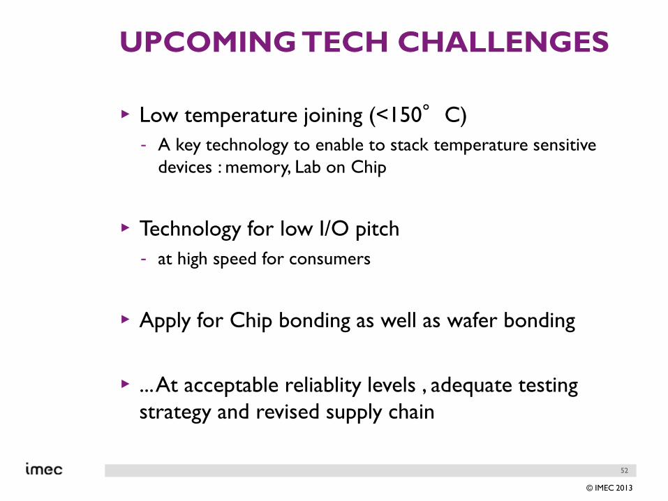
UPCOMING TECH CHALLENGES
▸ Low temperature joining (<150°C)
- A key technology to enable to stack temperature sensitive
devices : memory, Lab on Chip
▸ Technology for low I/O pitch
- at high speed for consumers
▸ Apply for Chip bonding as well as wafer bonding
▸ ... At acceptable reliablity levels , adequate testing
strategy and revised supply chain
53
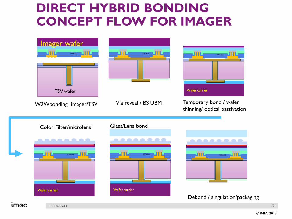
© IMEC 2013
P.SOUSSAN
DIRECT HYBRID BONDING CONCEPT FLOW FOR IMAGER
O3 TEOS
Imager wafer
W2Wbonding imager/TSV Via reveal / BS UBM
Color Filter/microlens Glass/Lens bond
Debond / singulation/packaging
O3 TEOS
FEOL
MEMS/Sensor wafer
O3 TEOS
TSV wafer
O3 TEOS
FEOL
MEMS/Sensor wafer
O3 TEOS
Wafer carrier
Temporary bond / wafer
thinning/ optical passivation
O3 TEOS
FEOL
MEMS/Sensor wafer
O3 TEOS
Wafer carrier
FEOL
O3 TEOS
Wafer carrier
O3 TEOS
FEOL
MEMS/Sensor wafer
O3 TEOS
Wafer carrier
FEOL
O3 TEOS
Wafer carrier
O3 TEOS
FEOL
MEMS/Sensor wafer
O3 TEOS
FEOL
O3 TEOS
Wafer carrier
54
© IMEC 2013
THANK YOU FOR YOUR ATTENTION
55
© IMEC 2013
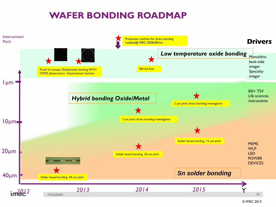
WAFER BONDING ROADMAP
P.SOUSSAN2012 2013 2014 Y
Interconnect
Pitch
10µm
1µm
Proof of concept Oxide/oxide bonding WITH
CMOS planarisation– Experimental machine
2015
Production machine for direct bonding
installed@ IMEC 200&300mm Drivers
Monolithic
back-side
imager
Specialty
imager
20µm
40µm Solder based bonding 40 µm pitch
BSI+ TSV
Life sciences
instruments
Sn solder bonding
BSI full flow
Solder based bonding 20 µm pitch
Solder based bonding 15 µm pitch
7 µm pitch direct bonding investigation
2 µm pitch direct bonding investigation
Hybrid bonding Oxide/Metal
Low temperature oxide bonding
MEMS
WLP
LED
POWER
DEVICES