3bb j - Solutions for micro and nano technologies · lighting, solar cells, displays, optical...
9
JePPIX ROADMAP 2012 | 1 The road to a multi-billion Euro market in InP-based Integrated Photonics JePPIX ROADMAP 2012 JePPIX Platform for Photonic Integration of InP-based Components and Circuits
Transcript of 3bb j - Solutions for micro and nano technologies · lighting, solar cells, displays, optical...

JePPIX ROADMAP 2012 | 1
The road to a multi-billion Euro market in InP-based Integrated Photonics
JePPIX ROADMAP 2012
JePPIXPlatform for Photonic Integration of InP-based Components and Circuits

2 | JePPIX ROADMAP 2012 JePPIX ROADMAP 2012 | 3
Prepared by
Meint Smit Mike Wale Dave Robbins Huub Ambrosius
on behalf of the JePPIX1 Steering Committee
1 JePPIX is the Joint European Platform for Photonic Integration of InP-based Components and Circuits. JePPIX partners are Europe’s leading chip and module manufacturers (Oclaro, FhG-HHI, CIP), photonic CAD companies (Phoenix, Photon Design, Filarete), equipment manufacturers (ASML, Aixtron, OCP) and R&D institutes (III-V Lab, COBRA-TU/e, Cambridge University and Politecnico di Milano). COBRA is coordinating JePPIX (www.jeppix.eu).
Executive Summary .............................................................................................. 4
Introduction: A revolution in Photonics ................................................................ 5
Applications ......................................................................................................... 6
The Ecosystem for Photonic Chips ....................................................................... 7
Technology Roadmap .......................................................................................... 8
Market Roadmap ................................................................................................. 9
Chip Cost Roadmap ............................................................................................10
R&D Roadmap ....................................................................................................11
Funding Roadmap ..............................................................................................12
Organisational Roadmap ....................................................................................13
SWOT analysis ....................................................................................................14
Appendix: Market Roadmap Assumptions ..........................................................15
Contents

4 | JePPIX ROADMAP 2012 JePPIX ROADMAP 2012 | 5
Introduction: A revolution in PhotonicsExecutive Summary
Photonics is a rapidly growing technology: LED-lighting, solar cells, displays, optical communica-tion, optical sensors and imaging are increasingly penetrating our world. Photonics has been recog-nized by the European Union as a Key Enabling Technology (KET), a technology that enables a mar-ket that is many times larger than the market of the technology itself. Micro and nanoelectronic integra-tion technology is an example of a KET which has a huge impact on our modern society; it is applied almost everywhere.
In 2007 a number of European key players in the field of Photonic Integration Technology started cooperation on development of highly standard-ized integration processes that can be used for a broad range of different applications, similar to the approach in microelectronics. These processes are called generic integration processes, and the ap-proach the generic foundry model.3�
Presently a number of large R&D projects are run-ning for developing generic foundry technologies and the infrastructure to make them accessible at low cost for a broad range of companies: design tools, component libraries, generic packaging tech-nology and generic test equipment. This model, in which Europe is clearly leading, will reduce the entry costs for companies that want to apply Photonic ICs in their products by more than an order of magni-tude. It will bring Photonic ICs (PICs) within reach for many SMEs and larger companies for which the entry costs of today’s technology are too high. In the coming years Generic Integration Technology is going to cause a revolution in the application of Photonic ICs, similar to what happened in micro-electronics thirty years ago.
At present the overall global Photonics market is about 10% of the electronics market. If pho-tonic integration technology is going to take a share of a few percent (comparable to the share of microelectronics in the electronics market) it will become a multi-billion market and enable an application market that is many times larger.
Figure 1 Microscope photograph of a Photonic IC for pulse compression in a bio-imaging microscope. Chip size is 6x6 mm2.
The present report is a first version in a series, it will be updated and improved on a yearly basis.
In the coming years the generic foundry approach will cause a revolution in micro and nanophotonics, just like it did in microelectronics thirty years ago. In Europe three integration technology platforms are active for introducing the generic foundry con-cept for the major integration technologies in Pho-tonics: JePPIX for InP-based monolithic integra-tion, ePIXfab for Silicon Photonics, and TriPleX for low-loss dielectric waveguide technology. In this report a roadmap for the development of generic InP-based integration technology is presented.
In microelectronics the MOSIS-program1 has been in-strumental in providing low-cost access to advanced foundry processes since the late eighties, first to universities, later also to companies. By processing more than 50,000 designs it has given a great boost to the development of VLSI technology. We foresee a similar two-phase development in photonic inte-gration: in a first phase low-cost access to advanced foundry processes is provided for R&D on integra-tion of existing or novel sub-systems into a single chip. We expect that a large number of universities and other research institutes will be interested in making use of such a facility. This number can even be increased by creating national design support centers in a number of countries throughout Europe. Many of these R&D designs will be developed in close cooperation with companies and a number of them will lead to commercial products, either from an existing company or a startup. This second phase will lead to a business, enabled by photonic ICs, which will exceed the 1 B€ level before 2020.
In this report the roadmap towards a multi-billion Euro market in generic InP-based Photonics is described. To make it happen the following steps have to be taken:• Enabling the JePPIX platform to take up an active
role in supporting ASPIC designers, explaining
the advantages of the generic approach to a large number of small and larger companies, scouting novel applications, and coordinating the R&D ef-fort that is required to maintain a dynamics with a steadily increasing performance at an essentially constant price, similar to Moore’s law in micro-electronics.
• Establishing a Network of national design sup-port centres throughout Europe coordinated by JePPIX.
• Creating investment funds for supporting AS-PIC development by small companies and novel technology development in a close cooperation between technology providers, academic and government research institutes.
Although the present roadmap vision is shared in large measure by all partners in the JePPIX platform, its realization is dependent on many uncertain fac-tors, both commercial and technological. Being an open access model to an enabling technology it will bring large benefits to a broad group of users. But an important uncertainty is the development of a proper business model to guarantee that sufficient funds can be made available to support the large investments that are required for development of novel technology generations with ever more perfor-mance. Here European and national public-private funding will be important to share part of the risks.
1 Pinã, C.A.: ‘Evolution of the MOSIS VLSI educational program’. Proc.First IEEE Int. Workshop on Electronic Design, Test and Applications (DELTA’02), Christchurch, New Zealand, 29–31 January 2002, pp. 187 – 191,
MOSIS website: www.mosis.com

6 | JePPIX ROADMAP 2012 JePPIX ROADMAP 2012 | 7
Successful introduction of a novel technology requires a close interaction between users and providers of the novel technology. Figure 3 depicts the main players in the eco-system.
At the heart are the generic foundries that provide cost-effective access to their high-performance technology. But the largest group, both in number and market vol-ume, is formed by companies using Photonic ICs in im-proved or novel products, for a variety of applications in telecom, datacom, sensing, security, medical diagnostics and metrology. Many of them are SMEs that do not have the expertise to design a chip themselves. A third key actor is, therefore, the group of PIC designers that forms the bridge between the users and the foundries by trans-lating the functional requirements of the users into a PIC design that can be processed in the foundry. This is quite similar to the model in microelectronics where design houses play an important role in making microelectronic technology also accessible to small companies. For the designers, to reduce their design time and the number of design cycles required, it is important to have dedi-cated design software with an accurate description of the foundry technology and accurate component librar-ies. The fourth key group provides the R&D that drives a dynamics similar to Moore’s law in electronics by de-veloping new generations of foundry technology with ever increasing performance, by developing increasingly powerful design software, component and sub-circuit
libraries, and by developing advanced Application Spe-cific Photonic ICs (ASPICs) for novel or improved user applications. For an effective development of the eco-system a coor-dinated approach (a broker) is necessary, which covers the following tasks:• Combining designs from different users on Multi-
Project Wafer (MPW) runs. In this way the costs of R&D runs can be shared by many users, which leads to a dramatic reduction of the entry costs.
• Organising proper documentation and training for the available foundry processes.
• Informing potential users and discussing the oppor-tunities that the novel technology brings for their product portfolio. Bringing them into contact with designers with expertise in their field.
• Developing and yearly updating a roadmap for the field.
• Stimulating cooperative research projects for mate-rialising the roadmap.
• Representing the JePPIX partners in national and European bodies.
In the FP6 Network of Excellence ePIXnet three plat-forms have been created for the most important generic technologies that, together, cover a major part of the applications market: JePPIX for InP-based monolithic integration technology, ePIXfab for Silicon Photonics technology, and TriPleX for low-loss high-Q dielectric waveguide technology. ePIXfab and JePPIX have taken up the brokering role in their fields, but without ade-quate funding for JePPIX. For TriPleX there is no broker yet, but there are good opportunities for combining this with JePPIX.
3 M. Smit, X. Leijtens, E. Bente, J. Van der Tol, H. Ambrosius, D. Robbins, M. Wale, N. Grote, M. Schell, “Generic foundry model for InP-based photonics”, IET Optoelectron, 2011, Vol. 5, Iss. 5, pp. 187–194, doi: 10.1049/iet-opt.2010.0068
The Ecosystem for Photonic Chips
The anticipated large reduction of R&D time and chip manufacturing costs will lead to a large growth of the share of Photonic ICs in the photonic components mar-ket. So far the use of PICs has been mainly restricted to specific areas in telecom core-network applications, where their specific functionality cannot be met by com-peting technologies. With the expected cost reduc-tions through a generic foundry approach, they will also become competitive in high volume markets like the telecom access network, where they can be applied in
the Central Office for integration of larger numbers of circuits that have to be repeated for each subscriber or group of subscribers. In future 10 Gb/s access networks they may also become competitive in the subscriber transceiver module.
When R&D and manufacturing costs drop, photonic chips will increasingly penetrate other applications. A good example is the fibre sensor market, which was over 400 M$ in 2008 with double digit annual growth figures. According to a recent GIO report it will exceed 2 B$ in 2015. A significant part of the sensor costs is in the readout unit, which contains one or more light sources, detectors and some signal processing circuitry. Here photonic ICs can replace a significant part of the exist-ing modules and enable novel sensor principles to be exploited. Examples are various types of strain sensors, heat sensors and a variety of chemical sensors.Optical Coherence Tomography is another potential ap-plication. Traditionally OCT is done in the 800 nm win-dow, which is the preferred choice for retina diagnostics. For skin or blood vessel diagnostics 1550 nm is a bet-ter wavelength, because there the penetration depth is three times as large due to reduced scattering losses at this wavelength. This provides good opportunities for InP PICs in OCT equipment.
Another interesting class of devices comprises pico and femtosecond pulse lasers. Here PICs containing mode locked lasers, optionally combined with pulse shapers, can provide small and cheap devices that can be used in widely differing applications, such as high-speed pulse generators and clock recovery circuits, ultrafast A/D-converters, and in multi-photon microscopy.These are just a few examples. Once ASPICs get to be really cheap, they will offer ample opportunity for small and large companies to improve their competitiveness by applying them in their products.
Applications
Figure 3 The main actors and their relations in the generic foundry ecosystem.
USERSAPPLICATIONS
PIC DESIGNERSDESIGN
SOFTWARE
PIC FOUNDRIESPACKAGING
BROKER(JEPPIX)
R&D
Figure 2 Widely tunable laser for application in optical co-herence tomography

8 | JePPIX ROADMAP 2012 JePPIX ROADMAP 2012 | 9
Due to significant investments in developing a foundry technology infrastructure (well over 50 M€ in European and national projects) Europe is making substantial progress towards establishing this new way of working. Figure 4 shows the roadmap for InP-based technology.
Since 2007 COBRA has provided small scale access to a first generation (G1) research platform. Process capabilities have been gradually improved and presently support de-sign of ASPICs integrating lasers, optical amplifiers, modu-lators and detectors with 10 Gb/s speed, and a variety of passive optical components. The platform is suitable for research and prototyping but not for volume production.
In 2009 the EuroPIC project began with the mission of transferring the foundry model from a university environ-ment to industrial and semi-industrial platforms (wafer fabs of Oclaro and FhG-HHI) and starting development of software design kits and standardized packaging solu-tions. The project has recently delivered its first chips from foundry trials relying on generic building block technolo-gy and is preparing a second full foundry run with access for a few external users to complete before the end of the project in 2012. After 2012 R&D will be started for quali-fication and further optimization of the process. Until the process will become commercially available, access to external users will be provided at a limited scale at a best-effort condition. Full commercial opera-tion can start after 2014, if the foundry model proves suf-ficiently viable at that time.
In 2010 the PARADIGM project has started with devel-opment of a second technology generation (G2) with
improved capabilities and performance: capability of providing both transmitter and receiver functions with operation up to 40 Gb/s, availability of superior lasers and amplifiers, wider choice of emission and detection wavelengths and other advanced features. The process will be competitive with advanced application-specific technology, but at a much lower cost. Further the proj-ect envisions development of low-cost generic packag-es and sophisticated software design kits with power-ful component and sub-circuit libraries. The processes should be demonstrated before the end of 2014. Dur-ing the project small scale access will be provided for selected external users. Assuming a viable business case, full commercial operation could start between 2016 and 2017, with earlier access for R&D purposes.
The next step will be the integration of photonics and electronics. Today the dominant approach for wafer-scale integration uses silicon for both the photonic and the electronic functionality.
As seen from Figure 5 InP is leading in circuit com-plexity, because of its superior properties for inte-grating lasers and optical amplifiers. It is, therefore, the material of choice for photonics, and silicon is the material of choice for electronics. COBRA recent-ly started research on a third generation (G3), which provides the same photonic functionality as G1 and G2 in an InP-based membrane-layer on top of a sili-con or CMOS substrate. If successful, it will become a successor of G2, offering efficient integration of photonic and electronic functionality. It is still in an early stage, however. Its commercialization is not ex-pected before 2020.
Technology Roadmap
The guiding model for the proposed approach is the US MOSIS program1 that made silicon VLSI tech-nology accessible to a broad community in the past decades (more than 50,000 designs). In a first phase it provided free access for universities to a num-ber of silicon foundry processes. This provided the program with a huge leverage; it attracted a large number of PhD students and other designers whose salaries were paid from other sources. A significant number of these designs have led to very successful products and companies and given a large boost to the development of VLSI technology. The model can be repeated in photonics with modest government investments. Figure 6 illustrates the market road-map. It can be divided in four phases.
Phase 1. In 2007 the COBRA institute of TU/e started providing small scale access for research purposes to its generic integration technology in the framework of the JePPIX platform (1 MPW-run with ~5 designs per year).
Phase 2. In 2009 and 2010 the JePPIX consortium started the EuroPIC and the PARADIGM projects for exploring the feasibility of transferring the generic approach from a university environment to industrial foundry platforms. These projects provide access to 10-20 internal and external designers per year in the period from 2011-2014, most of them from universi-ties and SMEs.
Phase 3. Within the JePPIX platform a plan for creat-ing national design centers for interesting and assist-ing novel university users has gained broad support. The plan foresees the setting up of seven JePPIX de-sign support centers, in addition to the Dutch cen-tre at COBRA, in the UK, Germany, France, Poland, Sweden, Italy and Spain. Other countries will follow. Figure 6 (R&D prototypes) shows a conservative es-timate of the number of designs that these national centers can generate by mobilizing and assisting in-terested designers from universities and companies. For taking off Phase 3 will need some modest Sup-port-Action like funding. Phase 4 is the production phase that will follow from successful business cases generated by phase 3. The market that will be generated in this phase is estimated to take off after 2015 and to exceed 1 B€ before 2020. The underlying assumptions are summa-rized in the Appendix.
1 See footnote on page 4
COBRA ResearchG1
2008 2010 2012 2014 2016 2018 20202006
G2 Commercial
G1 CommercialEuroPICindustrial platform
G1
PARADIGM industrial platform
G2
IMOS Research (COBRA)InP Membrane on SiliconG3
Figure 4 Roadmap for three generations of InP-based generic foundry technology
1
10
100
1000
1985 1990 1995 2000 2005 2010 2015
Co
mp
one
nt c
oun
t
InPSi
Figure 5 Complexity development of silicon and InP-based ICs.
Market Roadmap
Figure 6 Development of the ASPIC market
10 | JePPIX ROADMAP 2012 JePPIX ROADMAP 2012 | 11
Chip Cost Roadmap R&D Roadmap
Chip cost. Todays InP-technology is based on 3” wa-fers. A batch of 4 wafers has a usable chip area > 10,000 mm2. If we assume that the costs of such a batch are in the order of 100 k€, as an example for a process with moderate complexity, the chip cost will be in the order of 10 €/mm2. If the wafer volumes for foundry technol-ogy grow the costs will rapidly sink below 5 €/ mm2.
Chip cost for small ASPICS can thus get below 10 € already for small volumes. With the assumptions de-scribed above an ASPIC with more than 40 com-ponents on 6x6 mm2, as the one shown in Figure 1, will cost 350 €. This is a very small fraction of the cost of the individual discrete components (1 AWG demultiplexer, 20 SOAs and 20 phase modulators, estimated cost today 25-50 k€).
In the longer term (>10 yrs) further reduction below 1 €/mm2 may be expected by improving the fabrication process (yield) and increasing wafer and batch size. Yield of generic processes will compare favourably with application-specific ones because R&D invest-ments can be focused on standardized processes only.
Cost of a design run. For designing a complex AS-PIC on specs a few design runs may be required. By combining a number of designs on a so-called Multi-Project Wafer run the costs of a full run can be shared by several users and with the assumptions described above each user will pay around 200 € /mm2 for a chip set containing some 20 chips, which is usually sufficient for test purposes. Even for a design cycle of a few runs the chip costs remain affordable for many users. This compares very favourably with the devel-opment of an application specific process for a chip, which costs a few hundred thousands up to a few million Euro, dependent on the complexity of the process and the chip.
Cost of design. In the generic foundry approach the costs for developing a chip are no longer dominated by the chip cost but by the salary costs of the design-er who may need many months to come to a good design. These costs will also be strongly reduced, however, by the development of dedicated design kits with accurate libraries which allow for rapid and accurate chip design. As a result we expect that in the coming 5 years the design time will also be re-duced by a factor between two and five.
Packaging cost. Another important cost factor is the packaging of the chip. Already now the packaging costs are usually larger than the chip costs. This rela-tion will become even worse when the chips become much cheaper. The PARADIGM consortium is, there-fore, developing a standardized generic package for a broad class of different chips with standardized positions of the optical and electrical input and out-put ports. Costs of the packaging are expected to reduce to a few hundred Euro for small volumes and a few tens of Euros for very large volumes.
InP and Silicon Photonics. Due to the reduction of chip costs in a generic foundry model other costs, like the costs of design and packaging, will domi-nate the application costs. Because they are simi-lar for InP and Silicon photonic technology the cost per square mm of a technology is, up to a certain extent, less important than the functionality that it offers on that square mm. We see, therefore, excel-lent opportunities for InP for more complex circuitry, whereas Silicon may prove more competitive for less complex, very high-volume PICs. Hybrid combina-tion of both technologies will prove advantageous for both and is a good topic for a joint R&D effort. In the longer term we expect a merger of InP and Silicon technology, as depicted in Figure 4.
For a development in Photonics with a steady in-crease in performance and capabilities at constant or even decreasing costs (similar to Moore’s law in microelectronics) a continuing R&D investment pro-gram is necessary in the three fields indicated in Figure 3. They will be discussed subsequently.
Process technology and packaging R&D. Just as in silicon electronics, steady research in process tech-nology will lead to an ever increasing performance of the generic processes, through improvement of the existing processes and development of new technology generations. The R&D includes devel-opment of novel equipment which allows for better reproducibility and uniformity, and smaller features for higher integration densities, lower power con-sumption and higher speed.
Such investments, when focused on a few generic technologies, will broaden their market by out-performing many of the existing technologies, as CMOS did in microelectronics, and through the low chip costs that they offer they will create novel ap-plication fields.
Software and library R&D is important for short-ening the design cycle by developing accurate and comprehensive simulation of the ASPIC perfor-mance, so that only a few or even a single fabrica-tion run is sufficient to arrive at the required perfor-mance. R&D should be focused both on increasing the simulation and mask-layout generation capabili-ties of the software, and on development of accu-rate component and sub-circuit libraries. The for-mer will be the main responsibility of the software companies, the latter offers excellent opportunities for university-based research, in close cooperation with the foundries.
ASPIC-design. A third field of research is the de-velopment of ASPICs for specific user applications. Here universities will play an important role. In the coming years development of advanced ASPICs for specific applications will be an interesting task for PhD students, and a lot of the research that is pres-ently being done on development of discrete pho-tonic circuits and sub-systems will shift to develop-ment of ASPICs. This means that part of the funds available for component and system research may be directed towards development of generic AS-PICs, which will provide the foundry approach with a large leverage.
On the longer term we expect that ASPIC design will shift increasingly to companies and design houses, with universities remaining active on ASPIC development for advanced applications.
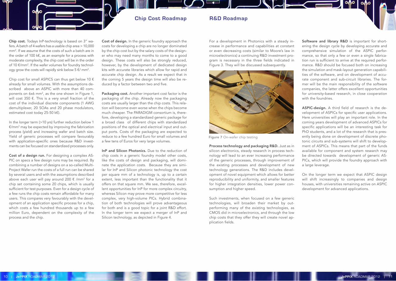
Figure 7 On-wafer chip testing

12 | JePPIX ROADMAP 2012 JePPIX ROADMAP 2012 | 13
Organisational Roadmap
Step 1. The most urgent funding priority is support for a JePPIX platform coordinator who can do the following jobs:• Combine designs of different users in Multi-
Project Wafer runs in the available processes.• Provide documentation of the available process-
es to new usersThe demand for participation in MPW runs, both from universities and companies, is larger than can be han-dled by the projects EuroPIC and PARADIGM. A JeP-PIX coordinator will arrange additional foundry runs and provide access to these runs for interested users. In ad-dition he should do the following tasks:• Informing potential users and discussing the oppor-
tunities that the novel technology brings for their product portfolio. Bringing them into contact with designers with expertise in their field.
• Yearly updating a roadmap for the field, in close cooperation with the JePPIX partners.
• Moderating business models and associated legal as-pects
• Stimulating cooperative research projects for mate-rialising the roadmap.
• Representing the JePPIX partners, where neces-sary, in national and European bodies
Appointing a JePPIX coordinator is a modest investment that will give the generic foundry development a large boost.
Step 2. A next step is the creation of national user sup-port centers throughout Europe, coordinated by JePPIX. This step is important to increase the number of design-ers and, thereby, the number of applications. See the quote of Lynn Conway in the blue box. There is already agreement with 7 partners on establishing such centers in the UK, France, Germany, Sweden, Italy, Spain and Poland. These centers can help interested users, both universities and companies in getting access to the foundry platforms. Setting up such centers can be done with modest investments, which should preferably come from Europe or national governments. They will have a huge leverage because they will (re)direct system ap-plications research, which is funded from other sources, from discrete to integrated solutions.
Phase 3. A third step, which should be undertaken paral-lel to phases 1 and 2, is to create public-private invest-ment funds for co-funding of research with a high risk or a
long time for return of investment. Such funds should be created both on a regional, national and European level. • National and regional funds should stimulate the
use of ASPICs by local companies. • European funds should stimulate investments in
foundry technology and infrastructure develop-ment for which the costs are too high to be carried by a single country and the risks are too high to be carried by a single company.
Such funding will be crucial for bridging the valley of death between the R&D prototype phase and the pro-duction phase as shown in Figure 6.
Project funding should address research in the three fields mentioned in the R&D roadmap:• Process technology, testing and packaging R&D• Software and library R&D• ASPIC-designProcess technology and packaging R&D is significantly more expensive than software and ASPIC develop-ment, and less suited for national funding, they should preferably be supported by creation of a European investment fund.
Selection of projects should preferably be done by a se-lection committee with a mix of national and European reviewers. The JePPIX platform can provide guidelines and support for evaluation of national and regional proj-ects in order to achieve a coherent European approach.For projects with public co-funding special attention should be paid to models that can, on a longer term, provide a return on investments from successful proj-ects, which can be re-invested in novel R&D. In this way the dependence on direct government funding will be reduced on the longer term.
Successful development of the foundry model re-quires an intensive cooperation between many part-ners in the eco-system. A good coordination is of key importance for the success of the novel approach. As the JePPIX platform is presently recognized as a coordinating body by all key players in the InP-based foundry approach it is the instrument par excellence for coordinating the future development.
At present JePPIX is an informal organization, sup-ported by TU/e and a few other partners on a volun-tary basis. It organizes yearly trainings in PIC-design, including some fabrication technology background, and it organizes MPW-runs on the COBRA research process, including designer support and assembly of the user designs in a single mask set. Another im-portant role is the coordination of existing and new R&D projects for further development of the foundry infrastructure. Finally, it is building a member group of users, from both universities and companies, that are interested in the use of ASPICs. At present this group counts already more than 8o users.
JePPIX is one of the three integration technol-ogy platforms that was created and funded by the ePIXnet Network of Excellence. After expiration of ePIXnet, funding of the Silicon Photonics platform ePIXfab was continued, but funding of the InP-based platform JePPIX and the dielectric waveguide plat-form TriPleX was stopped. Despite lack of funding the JePPIX platform has been extremely successful in bringing the InP-community together in a coher-ent effort for building a generic foundry technology infrastructure. For bridging the valley of death a similar funding as provided for the silicon photon-ics platform is highly desirable for enabling the JeP-PIX and the TriPleX platforms to take up the rapidly growing burden of user support.
Step 1: Appointment of a full-time coordinator with the tasks as described under “Funding Roadmap” (page 12)
Step 2: Establishment of national design support centers in a substantial number of European coun-tries. These centers should stimulate and assist na-tional users, both universities and companies, in getting access to the technology. Six universities, covering a major part of Europe, have expressed their interest in taking up this role5. In this approach the TriPleX platform can be integrated by establish-ing one or more TriPleX design support centers. The high degree of complementarity between InP and TriPleX technology would make this an interesting option.
Step 3: Establishing an investor board with both public and private investors in order to offer a spec-trum of funding opportunities that can match a vari-ety of business cases. In the first years a significant public funding effort will be necessary to cover the first years in which the returns on investment will be low (valley of death), as depicted in Figure 6.
5 UK (University of Cambridge), Germany (Karslruhe Institute of Technology), Sweden (KTH-Stockholm), Spain (UPV), Italy (Politecnico di Milano), Poland (Warsaw University of Technology). Discussions in other countries are in progress.
Funding Roadmap
“When new design methods are introduced in any technology, especially in a new technology, a large-scale exploratory application of the methods by many designers is necessary in order to test and validate the methods … A lot of usage is necessary to enable sufficient viewpoint shifts and social organization shifts to occur to effect the cultural integration of the methods.”
Lynn Conway, coauthor of the seminal text ‘Intro-duction to VLSI systems’ (1979), from PARC re-port ‘The MPC Adventures’ (1981)

14 | JePPIX ROADMAP 2012 JePPIX ROADMAP 2012 | 15
SWOT Analysis Appendix: Market Roadmap Assumptions
Strengths:
• Strong existing knowledge base• ASPIC Technology capable of meeting user
specifications now• Close, JePPIX-led, cooperation between the
main stakeholders• Clear lead over other (non EU) countries
Opportunities:
• Build dominant ASPIC based businesses in Europe
• Create clearly differentiated business chain º Design º Fab º Packaging º Software tools º Applications houses
• Achieve, straightforward, low cost access to ASPIC technology for all
Weaknesses:
• Too dependent on university sector• User base still too small, many companies
not aware of opportunities
Threats:
• InP fab operators cannot make necessary scale of investment, slowing progress
• Large strategic foreign government led in-vestments.
The market prediction as shown in Figure 6 is based on the assumption that the development of commer-cial ASPIC applications will take place in two phases.
In a first phase it will be university driven, just as in microelectronics in the MOSIS program. In the proj-ects EuroPIC and PARADIGM we see that many uni-versities are interested to get access to foundry pro-cesses. Many of them work in close cooperation with companies and a number of their designs will trans-late into commercial designs. This first phase can be launched with modest funding at the university side, because the major cost, salary cost for PhD students, will come from other existing or new projects, which will provide the investments in the foundry infrastruc-ture with a large leverage. Crucial to the success of this first phase is the availability and accessibility of the technological infrastructure, which requires large public-private investments on a European scale.
The second phase will typically start 2-3 years later, after the results of the first university designs be-come clear and a number of these design appear to be sufficiently promising for transfer to a company (either existing or a startup). As the companies will get little return on their investments during the first years public co-funding may prove vital for getting the wheel running. These investments can be done on a national or regional scale.
The quantitive assumptions underlying Figure 6 are as follows.
At present JePPIX users run 5-10 designs per year on the COBRA process (the blue bars in Figure 6 for 2009-2012). In the EuroPIC and the PARADIGM pro-cess 10-20 users (both internal and external) are de-signing in the experimental processes of Oclaro and Fraunhofer-HHI (the green bars). During and after EuroPIC and PARADIGM the design effort should be taken over and expanded by the national design sup-port centers mentioned in the organization roadmap.
These national centers will contribute an increasing number of ASPIC designs as indicated by the blue bars. Designs will come from both universities and companies, universities will play an important role in transferring this technology to companies.
It is assumed that 20% of the university designs will lead to a commercial design after 2 years (i.e. a de-sign which a company will develop further into a product). Further it is assumed that in 2014 the first commercial ASPICs will go into production. Further we assume that in the first five years the number of ASPICs which reach the production stage will double each year, which is realistic with an active platform dissemination policy. Further it is assumed that from the number of ASPICs in production in one year, 80% will still be exploited in the next year.
The data mentioned above refer to numbers of AS-PICs. For translation into a market figure we have assumed that 50% of the commercially successful designs (which is with the present assumptions only 10% of all R&D prototypes) generate a 10 M€/yr business after 2 years, while 20% generates a 100 M€/yr business after 3 years and 5 % a 500 M€ busi-ness after 4 years.
These assumptions lead to the prediction shown in Figure 6.

con
tact: co
ord
ina
tor@
jep
pix.e
u | d
esig
n: w
ww
.smit-vo
rmg
evin
g.n
l