380Vdc/48Vdc/ 3kw DC/DC converter with 98.2%...
6
380Vdc/48Vdc/ 3kw DC/DC converter with 98.2% efficiency Odd Roar Schmidt, Erik Myhre R&D, Eltek A/S Drammen, Norway Abstract — According to the Emerge Alliance, the interest for 380Vdc power distribution for data centres is growing. The DC distribution reduces the number of power conversion steps by utilizing a DC voltage of 380V; it provides a significant reduction of cable dimensions and associated costs. Some server board vendors have recently begun to initialize a move from a supply voltage of 12Vdc to 48Vdc. In order to make use of the new preferred voltage used by these vendors, DC/DC converters are required. In regards to the high and increasing power consumption of data centres, it is essential that such power converters are highly efficient. This paper presents a new topology of a 3kW DC/DC converter (380Vdc – 48Vdc) that boasts a conversion peak efficiency of 98.2%. The DC/DC converter is designed with a boost stage and an LLC DC/DC stage. As the converter is typically connected to a battery system consisting of 168 cells in a series, the converter can exploit the fact that the battery system provides 381Vdc in float operation. In normal float operation the DC input voltage is stable. This allows for the input voltage to be used directly as the DC link input to the LLC stage. That means that the BOOST-stage is not required in normal operation. However, during charge or discharge situations, the battery voltage may drop down to about 260Vdc, which would be too low as input voltage for an efficient LLC-stage. Therefore a BOOST stage is required to maintain a narrow band for voltage variations at the DC link from the BOOST -stage to the LLC-stage, in case of charge/discharge. The novelty of the proposed topology is therefore a built-in by- pass switch, using a MOSFET, where the BOOST stage is by- passed in normal operation, but actively used in the case of a battery voltage lower than a certain threshold. Keywords — High Efficiency DC-DC converter; ZVS, ZCS; Topology combination. I. INTRODUCTION The use of 380Vdc, for datacentre and central office, is growing according to Emerge Alliance. Both ETSI and Emerge Alliance have developed standards for 400Vdc distribution. The Emerge Alliance Data/Telecom Center standard describes the DC distribution [1] and ETSI has one standard 400Vdc distribution [2] and one for Earthing and Bonding [3]. Both standards specify a voltage range of 260 – 400Vdc with some transient conditions. This paper assumes 168 lead acid battery cells with a float voltage of 380.5Vdc at 20degC as standard. ABB has installed several data centres in Europe and the US with the following advantages as stated in [4] • 10% Better Energy Efficiency • 20% Lower Capital Cost • 25% Lower Footprint • 20% Lower Installation Cost The reliability of a 380Vdc system using batteries is very good and can be compared to a 48Vdc system for Telecom applications. The 380Vdc system contains more voltage convention stages to the server processor, than the 48Vdc system, and converts from 380Vdc to 48Vdc. It is currently possible to convert 48Vdc to 1.8Vdc for server processor utilization. From 380Vdc it is possible to have a down conversion to 1.8Vdc, but this is not available at the moment. The 380Vdc system will have at least two down conversion stages to 1.8Vdc, but the 48Vdc system will have one down conversion stage to 1.8Vdc. Reliability is normally dependent on the number of components, and the 380Vdc conversion to 1.8Vdc will have twice the components without significantly compromising reliability. At 380Vdc using batteries, the reliability can be improved with redundant converters from 380Vdc to 48Vdc, as either N+1 or N+N, depending on the system design. Redundant converters, from 48Vdc input to 1.8Vdc, will also improve reliability. The down converter is important to provide reliability and efficiency for the 380Vdc Power System. The most commonly used topology for a down converter is an LLC DC/DC converter in combination to use with a boost stage for a stable high output voltage in the range of 380Vdc to 425Vdc, which is the input voltage for the DC/DC converter. The DC/DC converter provides galvanic isolation. The converter can be a half, full-bridge, soft-switched/hard- switched or phase-shifted converter. 978-1-4799-6582-3/15/$31.00 ©2015 IEEE 130
Transcript of 380Vdc/48Vdc/ 3kw DC/DC converter with 98.2%...
380Vdc/48Vdc/ 3kw DC/DC converter with 98.2% efficiency
Odd Roar Schmidt, Erik Myhre R&D, Eltek A/S
Drammen, Norway
Abstract — According to the Emerge Alliance, the interest for 380Vdc power distribution for data centres is growing. The DC distribution reduces the number of power conversion steps by utilizing a DC voltage of 380V; it provides a significant reduction of cable dimensions and associated costs. Some server board vendors have recently begun to initialize a move from a supply voltage of 12Vdc to 48Vdc. In order to make use of the new preferred voltage used by these vendors, DC/DC converters are required. In regards to the high and increasing power consumption of data centres, it is essential that such power converters are highly efficient. This paper presents a new topology of a 3kW DC/DC converter (380Vdc – 48Vdc) that boasts a conversion peak efficiency of 98.2%. The DC/DC converter is designed with a boost stage and an LLC DC/DC stage. As the converter is typically connected to a battery system consisting of 168 cells in a series, the converter can exploit the fact that the battery system provides 381Vdc in float operation. In normal float operation the DC input voltage is stable. This allows for the input voltage to be used directly as the DC link input to the LLC stage. That means that the BOOST-stage is not required in normal operation. However, during charge or discharge situations, the battery voltage may drop down to about 260Vdc, which would be too low as input voltage for an efficient LLC-stage. Therefore a BOOST stage is required to maintain a narrow band for voltage variations at the DC link from the BOOST -stage to the LLC-stage, in case of charge/discharge. The novelty of the proposed topology is therefore a built-in by-pass switch, using a MOSFET, where the BOOST stage is by-passed in normal operation, but actively used in the case of a battery voltage lower than a certain threshold.
Keywords — High Efficiency DC-DC converter; ZVS, ZCS; Topology combination.
I. INTRODUCTION The use of 380Vdc, for datacentre and central office, is growing according to Emerge Alliance. Both ETSI and Emerge Alliance have developed standards for 400Vdc distribution. The Emerge Alliance Data/Telecom Center standard describes the DC distribution [1] and ETSI has one standard 400Vdc distribution [2] and one for Earthing and Bonding [3].
Both standards specify a voltage range of 260 – 400Vdc with some transient conditions. This paper assumes 168 lead acid battery cells with a float voltage of 380.5Vdc at 20degC as standard. ABB has installed several data centres in Europe and the US with the following advantages as stated in [4]
• 10% Better Energy Efficiency • 20% Lower Capital Cost • 25% Lower Footprint • 20% Lower Installation Cost
The reliability of a 380Vdc system using batteries is very good and can be compared to a 48Vdc system for Telecom applications. The 380Vdc system contains more voltage convention stages to the server processor, than the 48Vdc system, and converts from 380Vdc to 48Vdc. It is currently possible to convert 48Vdc to 1.8Vdc for server processor utilization. From 380Vdc it is possible to have a down conversion to 1.8Vdc, but this is not available at the moment. The 380Vdc system will have at least two down conversion stages to 1.8Vdc, but the 48Vdc system will have one down conversion stage to 1.8Vdc. Reliability is normally dependent on the number of components, and the 380Vdc conversion to 1.8Vdc will have twice the components without significantly compromising reliability. At 380Vdc using batteries, the reliability can be improved with redundant converters from 380Vdc to 48Vdc, as either N+1 or N+N, depending on the system design. Redundant converters, from 48Vdc input to 1.8Vdc, will also improve reliability. The down converter is important to provide reliability and efficiency for the 380Vdc Power System. The most commonly used topology for a down converter is an LLC DC/DC converter in combination to use with a boost stage for a stable high output voltage in the range of 380Vdc to 425Vdc, which is the input voltage for the DC/DC converter. The DC/DC converter provides galvanic isolation. The converter can be a half, full-bridge, soft-switched/hard-switched or phase-shifted converter.
978-1-4799-6582-3/15/$31.00 ©2015 IEEE 130
The overall efficiency is dependent on the two stages efficiency according to equation (1) Eff stage1 (%) x Eff stage 2(%) = Overall Eff (%) (1) Each stage is required to have the highest possible efficiency, so that the total efficiency can be as high as possible. If the efficiency of each stage is 98%, the overall efficiency will be 96% (1). To achieve 98% overall efficiency, each stage needs to have efficiency of 99%. The 380Vdc system voltage is suitable as the Bus voltage for a DC/DC converter, when the battery system is operating in float mode. Then the Boost stage can be bypassed and the efficiency can reach above 98%. When the batteries are in charge or discharge mode, the boost converter needs to be activated and support the DC/DC converter´s input voltage.
II. TOPOLOGY
A. Boost Topology The input voltage in a 380Vdc system ranges from 260Vdc to 400Vdc and a battery system of 168 cells in series provides approximately 381Vdc in float operation. The boost converter needs only to be active from 260Vdc to 376Vdc; above 376Vdc boost converter is switched off and bypassed. Since the battery provides a clean DC input, the boost topology can be built as a standard single switch boost and there is no need for a more complex bridgeless boost or PFC. See Figure 1
Figure 1 The boost topology L1 is the boost choke with freewheeling diode D1 and Switch 1, which is a MOSFET. The freewheeling diode D1 is a Silicon Carbide diode with very low forward voltage drop for highest efficiency. The only protection here is an RC snubber over the boost switch 1 and decoupling /snubber capacitor, C2, for the freewheeling diode. For the ON switching behavior of the topology, see
Figure 2.
Figure 2 On switching of boost switch, T= 2uS/div, A=4.2A/div, Vin=300Vdc,Vout=54.5Vdc and 40Adc. Worst case condition The recovery charge is fairly small due to the silicon carbide diode, which gives relative low peak current and switching losses. Efficiency at 1100W at 360Vdc is 97.5%.
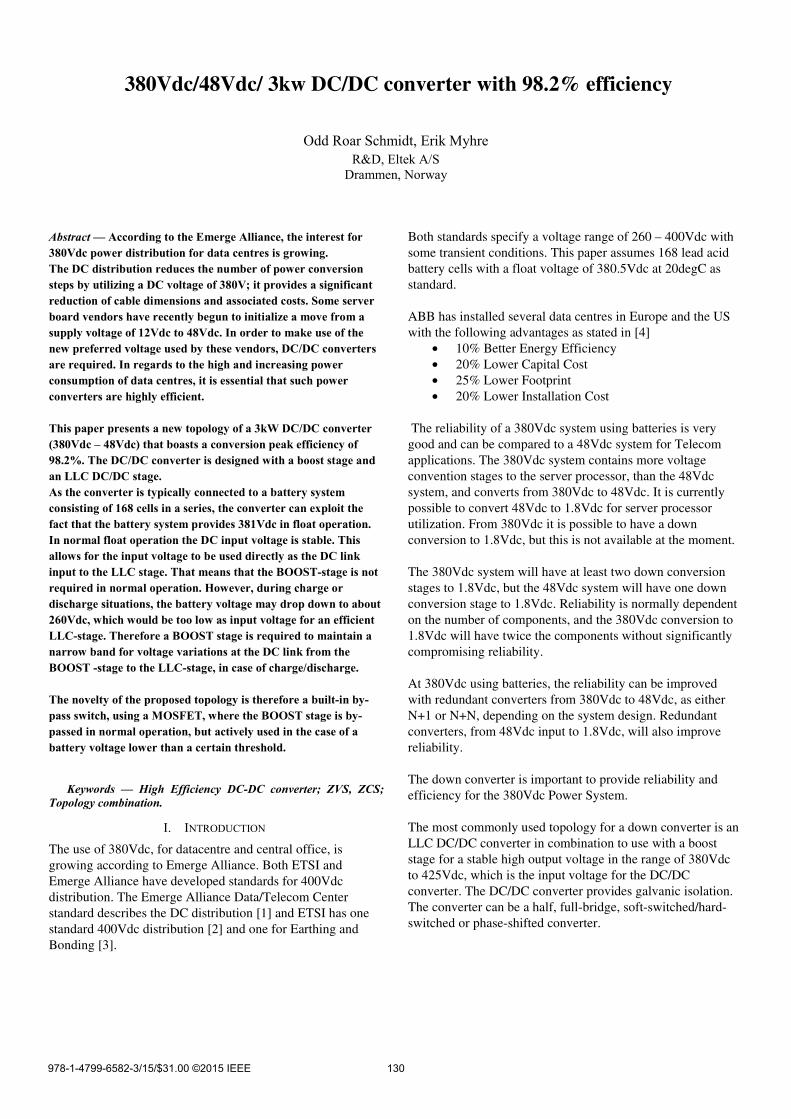
B. Bypass Switch See Figure 3, bypass switch and boost topology. Switch 2, which is a 650V MOSFET, it is controlled on/off by the input voltage.
Figure 3 Bypass switch and boost circuit The gate drive to the Bypass Switch is implemented with a high side Gate driver. The on/off control of the Bypass Switch can be done either by using a Primary, Digital Signal Processor, DSP or an analog approach with a comparator. The final solution for this approach will be disclosed further below in this paper.
131
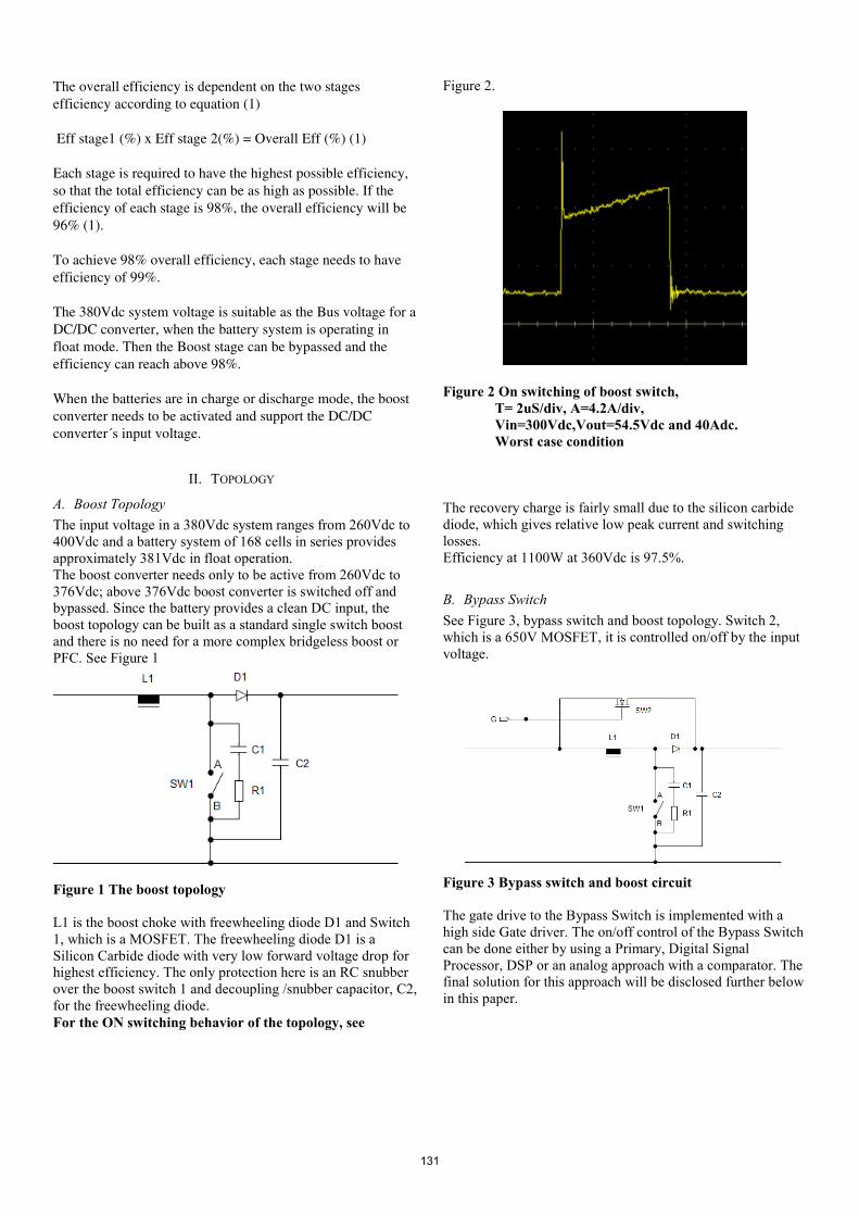
C. DC/DC Topology The proposed DC/DC topology is an LLC converter working in inductive mode, above the resonance frequency. The topology used in the DC/DC converter has been a standard building block in Eltek for several decades. With the LLC converter, it is possible to achieve a very high efficiency of up to 99%. The key to achieve this level of efficiency is the control of the LLC with frequency, dead time control and ZVS. A condition required to achieve extremely high efficiency is constant input and output voltage. If the input voltage varies, it makes the control more complex, and efficiency is affected negatively. A good result is however obtainable. It is possible to run the LLC with a input voltage window of 375Vdc to 400Vdc, with a fixed output voltage of 53.5Vdc.
In addition, it is possible to have an output voltage window regulation as well. However, an output voltage window can be negatively affected under no load condition. The LLC circuit shown in Figure 4, with the half bridge MOSFET switches, SW 1 and 2, is switching with ZVS during switching on and due to the snubber capacitors C2 and C3 almost ZVS in turning off. The LLC converter has rectifying diodes on the output See Figure 4. Nevertheless, the LLC converter has Synchronous Rectifying MOSFET, replacing the conventional diodes for optimizing the efficiency.
Figure 4 LLC converter
132

The half bridge MOSFET switches, SW 1 and 2, are switching with ZVS during switching on and due to the snubber capacitors C2 and C3 almost ZVS in turning off. See Figure 5 for the bottom Switch 2 with MOSFET, internal body diode and snubber capacitor.
Figure 5 MosFet Switch2 The LLC converter needs a frequency and dead time control as function of frequency to operate as a soft switching converter. It is important to ensure that the converter is operating in soft switching mode under all possible conditions, ensuring maximum efficiency, EMI performance and reliability.
Figure 6 Voltage and Current waveform of Switch 2 See Figure 6 for the voltage and current waveforms of MOSFET Switch 2. When the upper Switch 1 is turned off (See Figure 4 LLC converter) the current will continue to flow into the transformer and charge snubber capacitor C2 and discharge snubber capacitor C3. When the voltage goes to 0Vdc over Switch 2, the internal diode of Switch 2 starts to conduct. The MOSFET of Switch 2 is then turned before the current goes to 0A at time tb.
The ON switching of the MOSFET is now done with zero voltage. When the snubber capacitor C2 is charged, and C3 is discharged with magnetizing load current this is almost a ZVS at turn off of the upper MOSFET Switch 1. If the design and control of the LLC is done correctly, the switching losses will be very small in the MOSFET switches. In case the MOSFET Switch 2 is turned on before the diode starts to conduct, the MOSFET Switch 1 and 2 will switch with high current and voltage. Hard switching with high voltage and current will result in poor or reduced EMI performance and will result in a very large impact on reliability. The magnetizing inductor will assist with current for ZVS and the input-output voltage regulation window [5][6]. In addition, the magnetizing inductor with the LLC resonance components forms a parallel resonance frequency below the LLC resonance frequency. The parallel resonance circuit can be used to boost the output power or increase holdup time. The secondary output of the LLC transformer midpoint is connected to two rectifier diodes or, as used in this case, to two synchronous MOSFET for rectification. See Figure 7 for the ripple current in the output capacitor C4.
Figure 7 Ripple current output capacitor C4
The ripple current in this capacitor is approximately 48.5% of the DC output current. In comparison, the latest generation electrolytic capacitor is able handle the ripple current while maintaining a long life cycle.
If an interleaved solution is used with two phase-shifted LLC stages, the ripple current is reduced to approximately 10.5%. One possible advantage is that the efficiency curve can be wider, but less cost effective.
III. BYPASS SWITCH The bypass switch will ensure the best possible efficiency during normal float condition. The boost stage is bypassed by a MOSFET and makes sure that only the LLC converter is operating at maximum efficiency. The Bypass Switch and Boost stage are shown in Figure 8.
133
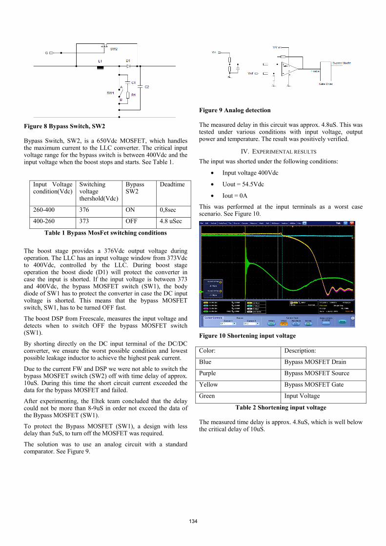
Figure 8 Bypass Switch, SW2 Bypass Switch, SW2, is a 650Vdc MOSFET, which handles the maximum current to the LLC converter. The critical input voltage range for the bypass switch is between 400Vdc and the input voltage when the boost stops and starts. See Table 1.
Input Voltage condition(Vdc)
Switching voltage thershold(Vdc)
Bypass SW2
Deadtime
260-400 376 ON 0,8sec
400-260 373 OFF 4.8 uSec
Table 1 Bypass MosFet switching conditions
The boost stage provides a 376Vdc output voltage during operation. The LLC has an input voltage window from 373Vdc to 400Vdc, controlled by the LLC. During boost stage operation the boost diode (D1) will protect the converter in case the input is shorted. If the input voltage is between 373 and 400Vdc, the bypass MOSFET switch (SW1), the body diode of SW1 has to protect the converter in case the DC input voltage is shorted. This means that the bypass MOSFET switch, SW1, has to be turned OFF fast.
The boost DSP from Freescale, measures the input voltage and detects when to switch OFF the bypass MOSFET switch (SW1).
By shorting directly on the DC input terminal of the DC/DC converter, we ensure the worst possible condition and lowest possible leakage inductor to achieve the highest peak current.
Due to the current FW and DSP we were not able to switch the bypass MOSFET switch (SW2) off with time delay of approx. 10uS. During this time the short circuit current exceeded the data for the bypass MOSFET and failed.
After experimenting, the Eltek team concluded that the delay could not be more than 8-9uS in order not exceed the data of the Bypass MOSFET (SW1).
To protect the Bypass MOSFET (SW1), a design with less delay than 5uS, to turn off the MOSFET was required.
The solution was to use an analog circuit with a standard comparator. See Figure 9.
Figure 9 Analog detection The measured delay in this circuit was approx. 4.8uS. This was tested under various conditions with input voltage, output power and temperature. The result was positively verified.
IV. EXPERIMENTAL RESULTS The input was shorted under the following conditions:
• Input voltage 400Vdc
• Uout = 54.5Vdc
• Iout = 0A
This was performed at the input terminals as a worst case scenario. See Figure 10.
Figure 10 Shortening input voltage
Color: Description:
Blue Bypass MOSFET Drain
Purple Bypass MOSFET Source
Yellow Bypass MOSFET Gate
Green Input Voltage
Table 2 Shortening input voltage
The measured time delay is approx. 4.8uS, which is well below the critical delay of 10uS.
134

See Figure 11 for the efficiency measured at 380.5Vdc input and 54.5Vdc output voltage.
Figure 11 Efficiency at 380.5Vdc input voltage
At approx. 1100W, the efficiency is 98.2%.
The efficiency drops when the boost kicks in but a reasonable efficiency is still observed. In regards to that this condition only occurs under discharge/charge of the batteries.
.
Figure 12 Efficiency at 360.0Vdc input voltage
Peak efficiency at 1100W is maintained in the 97.5% range
V. CONCLUTION The AC/DC converter and DC/DC converter operate very differently in regards to input voltage. The AC/DC converter has in normal operation a wide input voltage range to cover (in worst case from 90 to 300Vac) and it gives a regulated output voltage with high efficiency. A DC/DC converter used in 380Vdc system normally has a stable input voltage, due to the batteries on the DC bus.
The input voltage to the DC/DC converter is only changing during the batteries’ charge and discharge cycles.
This ensures the possibility to use a MOSFET Switch to bypass the boost stage in order to maximize the efficiency. In this case, it was possible to achieve 98.2% efficiency at 1100W output power.
With the boost stage running at 360Vdc, the overall efficiency is approximately 97.5%, which is still good. In this case the efficiency of the boost stage is above 99%.
In the future it will be possible to drive the efficiency of the LLC above 99% by fine tuning and using an interleaved solution.
Boost circuit is heavily dependent on a better SiC diode for further improvement of efficiency
REFERENCES [1] EMerge Alliance Data/Telecom Center Standard Version 1.02. [2] ETSI EN 300 132-3-1 V2.1.1. [3] ETSI EN 300 605 V1.1.1. [4] ABB review 4/13, the corperate technical journal, Datacenters,pp 16-21 [5] Design Considerations for an LLC Resonant Converter, Hangseok Choi
Fairchild Semiconductor 82-3, Dodang-dong, Wonmi-gu Bucheon-si, Gyeonggi-do, Korea.
[6] High Efficiency Optimization of LLC Resonant Converter for Wide Load Range. Ya Liu, Virginia Polytechnic Institute and State University, December 4th, 2007 Blacksburg, Virginia.
135