32 Hardware Manual The revision list can be viewed...
923
Renesas 32-Bit Single-Chip RISC Microprocessor SuperH RISC engine Family/SH7040 Series (CPU Core SH-2) Rev.6.00 2003.5.26 SH7040, SH7041, SH7042, SH7043, SH7044, SH7055 Group Hardware Manual 32
Transcript of 32 Hardware Manual The revision list can be viewed...

Renesas 32-Bit Single-Chip RISC MicroprocessorSuperH RISC engine Family/SH7040 Series
(CPU Core SH-2)
SH7040, SH7041, SH7042,SH7043, SH7044, SH7055 Group
Hardware Manual32
Rev.6.002003.5.26
Unknown
The revision list can be viewed directly by clicking the title page. The revision list summarizes the locations of revisions and additions. Details should always be checked by referring to the relevant text.


Renesas 32-Bit Single-Chip RISCMicroprocessor
SuperH RISC engine Family/SH7040 Series (CPU Core SH-2)
SH7040, SH7041, SH7042,SH7043, SH7044, SH7055
Group
Hardware Manual
REJ09B0044-0600O

Cautions
Keep safety first in your circuit designs!
1. Renesas Technology Corporation puts the maximum effort into making semiconductor products better and more reliable, but
there is always the possibility that trouble may occur with them. Trouble with semiconductors may lead to personal injury, fire or
property damage.
Remember to give due consideration to safety when making your circuit designs, with appropriate measures such as (i) placement
of substitutive, auxiliary circuits, (ii) use of nonflammable material or (iii) prevention against any malfunction or mishap.
Notes regarding these materials
1. These materials are intended as a reference to assist our customers in the selection of the Renesas Technology Corporation
product best suited to the customer's application; they do not convey any license under any intellectual property rights, or any
other rights, belonging to Renesas Technology Corporation or a third party.
2. Renesas Technology Corporation assumes no responsibility for any damage, or infringement of any third-party's rights,
originating in the use of any product data, diagrams, charts, programs, algorithms, or circuit application examples contained in
these materials.
3. All information contained in these materials, including product data, diagrams, charts, programs and algorithms represents
information on products at the time of publication of these materials, and are subject to change by Renesas Technology
Corporation without notice due to product improvements or other reasons. It is therefore recommended that customers contact
Renesas Technology Corporation or an authorized Renesas Technology Corporation product distributor for the latest product
information before purchasing a product listed herein.
The information described here may contain technical inaccuracies or typographical errors.
Renesas Technology Corporation assumes no responsibility for any damage, liability, or other loss rising from these inaccuracies
or errors.
Please also pay attention to information published by Renesas Technology Corporation by various means, including the
Renesas Technology Corporation Semiconductor home page (http://www.renesas.com).
4. When using any or all of the information contained in these materials, including product data, diagrams, charts, programs, and
algorithms, please be sure to evaluate all information as a total system before making a final decision on the applicability of the
information and products. Renesas Technology Corporation assumes no responsibility for any damage, liability or other loss
resulting from the information contained herein.
5. Renesas Technology Corporation semiconductors are not designed or manufactured for use in a device or system that is used
under circumstances in which human life is potentially at stake. Please contact Renesas Technology Corporation or an
authorized Renesas Technology Corporation product distributor when considering the use of a product contained herein for any
specific purposes, such as apparatus or systems for transportation, vehicular, medical, aerospace, nuclear, or undersea repeater
use.
6. The prior written approval of Renesas Technology Corporation is necessary to reprint or reproduce in whole or in part these
materials.
7. If these products or technologies are subject to the Japanese export control restrictions, they must be exported under a license
from the Japanese government and cannot be imported into a country other than the approved destination.
Any diversion or reexport contrary to the export control laws and regulations of Japan and/or the country of destination is
prohibited.
8. Please contact Renesas Technology Corporation for further details on these materials or the products contained therein.
Preface
The SH7040 Series (SH7040, SH7041, SH7042, SH7043, SH7044, SH7045) single-chip RISC(Reduced Instruction Set Computer) microprocessors integrate a Renesas Technology-originalRISC CPU core with peripheral functions required for system configuration.
The CPU has a RISC-type instruction set. Most instructions can be executed in one clock cycle,which greatly improves instruction execution speed. In addition, the 32-bit internal-busarchitecture enhances data processing power. With this CPU, it has become possible to assemblelow cost, high performance/high-functioning systems, even for applications that were previouslyimpossible with microprocessors, such as real-time control, which demands high speeds. Inparticular, the SH7040 series has a 1-kbyte on-chip cache, which allows an improvement in CPUperformance during external memory access.
In addition, the SH7040 series includes on-chip peripheral functions necessary for systemconfiguration, such as large-capacity ROM and RAM, timers, a serial communication interface(SCI), an A/D converter, an interrupt controller, and I/O ports. Memory or peripheral LSIs can beconnected efficiently with an external memory access support function. This greatly reducessystem cost.
There are versions of on-chip ROM: mask ROM, PROM, and flash memory. The flash memorycan be programmed with a programmer that supports SH7040 series programming, and can alsobe programmed and erased by software.
This hardware manual describes the SH7040 series hardware. Refer to the programming manualfor a detailed description of the instruction set.
Related Manual
SH7040 series instructions
SH-1/SH-2/SH-DSP Programming Manual
Please consult your Renesas Technology sales representative for details for developmentenvironment system.

List of Items Revised or Added for This Version
Section Page Description
1.1.1 SH7040 SeriesFeatures
Notes on theSH7040 SeriesSpecifications
7,9
Note: Package with Copper used as the lead material.
Type Abbreviation Package Frequency Voltage Type Name ROMMask Version
On-chip ROM
External Bus Width
Operating Temp
ElectricalCharacteristics
A/D Accuracy (5Vversion)
Notes on the SH7040 Series Specifications
ZTAT SH7042 128 kB 16 bits ±15LSB(High-Speed)
QFP2020-112 –20°C to 75°C 28 MHz16 MHz
5 V3.3 V
HD6477042F28HD6477042VF16
See “128 kBPROM”
See “Electrical Characteristics”
FLASH SH7044F 256 kB 16 bits ±4LSB(Mid-Speed)
QFP2020-112 –20°C to 75°C 28 MHz 5 V HD64F7044F28 See “256 kB Flash Memory”
See “Electrical Characteristics”
SH7042A A mask
A mask
MASK SH7040A 64 kB 16 bits ±4LSB(Mid-Speed)
QFP2020-112
TQFP1414-120QFP2020-112Cu*
–20°C to 75°C 28 MHz16 MHz16 MHz 28 MHz16 MHz
5 V3.3 V3.3 V 5 V3.3 V
HD6437040AF28HD6437040AVF16HD6437040AVX16
HD6437040ACF28HD6437040AVCF16
See “64 kB Mask ROM”
See “Electrical Characteristics”
A mask
ROM less
SH7040A 16 bits ±4LSB(Mid-Speed)
QFP2020-112
TQFP1414-120QFP2020-112Cu*
–20°C to 75°C 28 MHz16 MHz16 MHz28 MHz16 MHz
5 V3.3 V3.3 V5 V3.3 V
HD6417040AF28HD6417040AVF16HD6417040AVX16 HD6417040ACF28HD6417040AVCF16
See “Electrical Characteristics”
A mask
128 kB 16 bits ±4LSB(Mid-Speed)
QFP2020-112
TQFP1414-120QFP2020-112Cu*
–20°C to 75°C 28 MHz16 MHz16 MHz
28 MHz16 MHz
5 V3.3 V3.3 V
5 V3.3 V
HD6477042AF28HD6477042AVF16HD6477042AVX16
HD6477042ACF28HD6477042AVCF16
See “128 kB PROM”
See “Electrical Characteristics”
SH7043 128 kB 32 bits ±15LSB(High-Speed)
QFP2020-144 –20°C to 75°C 28 MHz16 MHz
5 V3.3 V
HD6477043F28HD6477043VF16
See “128 kB PROM”
See “Electrical Characteristics”
SH7043A A mask 128 kB 32 bits ±4LSB(Mid-Speed)
QFP2020-144
QFP2020-144Cu*
–20°C to 75°C 28 MHz16 MHz
28 MHz16 MHz
5 V3.3 V
5 V3.3 V
HD6477043AF28HD6477043AVF16
HD6477043ACF28HD6477043AVCF16
See “128 kB PROM”
See “Electrical Characteristics”
SH7045F A mask 256 kB 32 bits ±4LSB(Mid-Speed)
QFP2020-144 –20°C to 75°C 28 MHz 5 V HD64F7045F28 See “256 kB Flash Memory”
See “Electrical Characteristics”
SH7041A A mask 64 kB 32 bits ±4LSB(Mid-Speed)
QFP2020-144
QFP2020-144Cu*
–20°C to 75°C 28 MHz16 MHz
28 MHz16 MHz
5 V3.3 V
5 V3.3 V
HD6437041AF28HD6437041AVF16
HD6437041ACF28HD6437041AVCF16
See “64 kB Mask ROM”
See “Electrical Characteristics”
SH7042A A mask 128 kB 16 bits ±4LSB(Mid-Speed)
QFP2020-112
TQFP1414-120QFP2020-112Cu*
–20°C to 75°C 28 MHz16 MHz16 MHz
28 MHz16 MHz
5 V3.3 V3.3 V
5 V3.3 V
HD6437042AF28HD6437042AVF16HD6437042AVX16
HD6437042ACF28HD6437042AVCF16
See “128 kB Mask ROM”
See “Electrical Characteristics”
SH7043A A mask 128 kB 32 bits ±4LSB(Mid-Speed)
QFP2020-144
QFP2020-144Cu*
–20°C to 75°C 28 MHz16 MHz
28 MHz16 MHz
5 V3.3 V
5 V3.3 V
HD6437043AF28HD6437043AVF16
HD6437043ACF28HD6437043AVCF16
See “128 kB Mask ROM”
See “Electrical Characteristics”
SH7044 A mask 256 kB 16 bits ±4LSB(Mid-Speed)
QFP2020-112 –20°C to 75°C 28 MHz 5 V HD6437044F28 See “256 kB Mask ROM”
See “Electrical Characteristics”
SH7045 A mask 256 kB 32bits ±4LSB(Mid-Speed)
QFP2020-144 –20°C to 75°C 28 MHz 5 V HD6437045F28 See “256 kB Mask ROM”
See “Electrical Characteristics”
SH7041A A mask 32 bits ±4LSB(Mid-Speed)
QFP2020-144
QFP2020-144Cu*
–20°C to 75°C 28 MHz16 MHz
28 MHz16 MHz
5 V3.3 V
5 V3.3 V
HD6417041AF28HD6417041AVF16
HD6417041ACF28HD6417041AVCF16
See “Electrical Characteristics”
SH7042 128 kB 16 bits ±15LSB(High-Speed)
QFP2020-112 –20°C to 75°C 28 MHz16 MHz
5 V3.3 V
HD6437042F28HD6437042VF16
See “128 kB Mask ROM”
See “Electrical Characteristics”
SH7043 128 kB 32 bits ±15LSB(High-Speed)
QFP2020-144 –20°C to 75°C 28 MHz16 MHz
5 V3.3 V
HD6437043F28HD6437043VF16
See “128 kB Mask ROM”
See “Electrical Characteristics”
1.4 The F-ZTATVersion OnboardProgramming
Figure 1.6 ConditionTransfer for FlashMemory
42 Note amended
Notes: For transferring between user mode and user program mode, proceed while CPU is not programming or erasing the flash memory.* RAM emulation permitted
2.4 Instruction Setby Classification
Table 2.16 BranchInstructions
70 Table amended
BF/S label 10001111dddddddd Delayed branch, if T = 0, disp × 2 +PC → PC; if T = 1, nop
2/1* —
4.2.3 Notes onBoard Design
— Deleted
4.5 Usage Notes 83 to85
Newly added
11.1.4 RegisterConfiguration
Table 11.2 DMACRegisters
218 Note * 5 deleted

Section Page Description
11.2.3 DMATransfer CountRegisters 0–3(DMATCR0–DMATCR3)
220 Description amended
The data for the upper 8 bits of a DMATCR is 0 when read.
11.2.4 DMAChannel ControlRegisters 0–3(CHCR0–CHCR3)
221 Description amended
• Bits 31–21—Reserved bits: Data are 0 when read. The writevalue always be 0.
224 Description amended
• Bit 7—Reserved bits: Data is 0 when read. The write valuealways be 0.
11.2.5 DMACOperation Register(DMAOR)
226 Description amended
• Bits 15–10—Reserved bits: Data are 0 when read. The writevalue always be 0.
227 Description amended
• Bits 7–3—Reserved bits: Data are 0 when read. The writevalue always be 0.
11.3.3 ChannelPriority
Figure 11.3 RoundRobin Mode
233 Figure amended
Channel 0 is given the lowestpriority.
12.4.5 CascadeConnection Mode
Figure 12.23Cascade ConnectionOperation Example(Phase CountingMode)
337 Figure amended
TCLKC
TCLKD
12.4.9ComplementaryPWM Mode
Figure 12.55Example of OutputPhase Switching byExternal Input (1)
373 Figure amended
When BDC = 1, N = 0, P = 0, FB = 0, output active level = high

Section Page Description
12.9.2 BlockDiagram
Figure 12.125 POEBlock Diagram
444 Note added
TIOC3B*
TIOC3D*
TIOC4A*
TIOC4C*
TIOC4B*
TIOC4D*
Note: * Includes multiplexed pins.
12.11.5 UsageNotes
453 Section added
14.2.8 Bit RateRegister (BRR)
Table 14.3 Bit Ratesand BRR Settings inAsynchronous Mode(cont)
491 Table amended
Bit Rate 27.0336
(Bits/s) n N Error (%)
110 3 119 0.00
150 3 87 0.00
300 2 175 0.00
600 1 87 0.00
1200 1 175 0.00
2400 1 87 0.00
4800 0 175 0.00
9600 0 87 0.00
14400 0 58 –0.56
19200 0 43 0.00
28800 0 28 1.15
31250 0 26 0.12
38400 0 21 0.00
Table 14.4 Bit Ratesand BRR Settings inClockedSynchronous Mode(cont)
495 Table amended3.5M — — — — 0 1
5M 0 0* — — — —
7M — — 0 0*
14.3.4 ClockSynchronousOperation
Figure 14.22Example of SCIReceive Operation
529 Figure amended
Bit 7 Bit 0
RxI request

Section Page Description
15.4.9 A/DConversion Time
Table 15.8Operating Frequencyand CKS Bit Settings
562 33 MHz deleted
15.6 Notes on Use
Figure 15.14Example of aProtection Circuit forthe Analog Input Pins
564 Figure amended
Notes: Numbers are only to be noted as reference value
*1
*2 Rin: Input impedance
AVss
AVcc
AVref
AN0 to AN7
This LSI
10µF 0.01µF
100ΩRin*2
0.1µF*1*1
16.7.2 Handling ofAnalog Input Pins
Figure 16.8 Exampleof Analog Input PinProtection Circuit
585 Note amended
Notes: Numbers are only to be noted as reference value
19.2 Port A
Table 19.2 Port A,FP-144 Version
649 Table amended
PA16 (I/O)/AH (output) PA16 (I/O)/AH (output) PA16 (I/O)
PA15 (I/O)/CK (output) PA15 (I/O)/CK (output) PA15 (I/O)/CK (output)
21.2.2 SocketAdapter PinCorrespondence andMemory Map
Figure 21.2 SH7042Pin and HN27C101Pin Correspondence(112-Pin Version)
671 Figure amended2 nF
100 Ω
0.1 µF

Section Page Description
21.2.2 SocketAdapter PinCorrespondence andMemory Map
Figure 21.3 SH7042Pin and HN27C101Pin Correspondence(120-Pin Version)
672 Figure amended2 nF
0.1 µF
100 Ω
Figure 21.4 SH7043Pin and HN27C101Pin Correspondence(144-Pin Version)
673 Figure amended
100 Ω
0.1 µF
2 nF
22.2.2 ModeTransition Diagram
Figure 22.2 FlashMemory ModeTransitions
683 Note amended
Execute transition between the user mode and user program modewhile the CPU is not programming or erasing the flash memory
Section Page Description
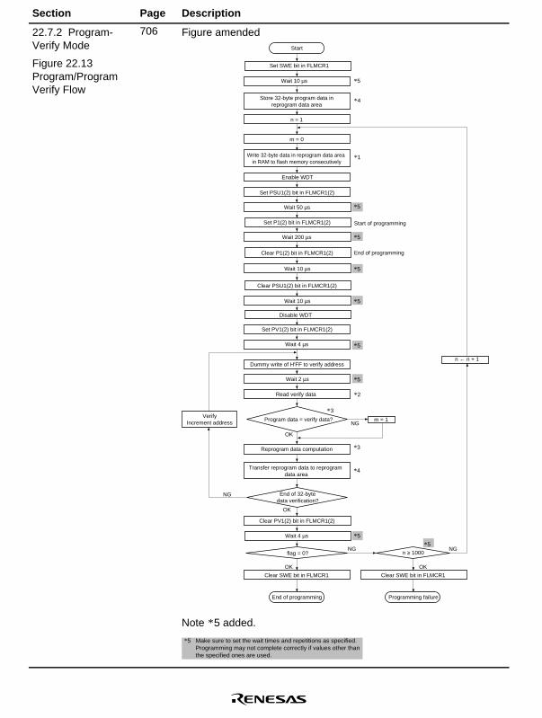
22.7.2 Program-Verify Mode
Figure 22.13Program/ProgramVerify Flow
706 Figure amended
Set SWE bit in FLMCR1
n = 1
m = 0
Write 32-byte data in reprogram data area in RAM to flash memory consecutively
Start of programming
NG
NG
NG NG
OK
OK
OK
*2
*5
*5
*5
*5
*5
*5
*5
*5
*5
Store 32-byte program data inreprogram data area
*4
*1
*5
Read verify data
Clear SWE bit in FLMCR1
m = 1
End of programming
Program data = verify data?
End of 32-bytedata verification?
flag = 0?
VerifyIncrement address
OK
Clear SWE bit in FLMCR1
n ≥ 1000
n ← n + 1
Start
*3
*3
*4
Enable WDT
Disable WDT
Reprogram data computation
Transfer reprogram data to reprogram data area
Wait 10 µs
Clear PV1(2) bit in FLMCR1(2)
Wait 4 µs
Dummy write of H'FF to verify address
Wait 2 µs
Set PV1(2) bit in FLMCR1(2)
Wait 4 µs
Clear PSU1(2) bit in FLMCR1(2)
Wait 10 µs
Clear P1(2) bit in FLMCR1(2)
Wait 10 µs
Set P1(2) bit in FLMCR1(2)
Wait 200 µs
Set PSU1(2) bit in FLMCR1(2)
Wait 50 µs
Programming failureEnd of programming
Note * 5 added.
*5 Make sure to set the wait times and repetitions as specified. Programming may not complete correctly if values other than the specified ones are used.

Section Page Description
22.7.4 Erase-VerifyMode
Figure 22.14Erase/Erase-VerifyFlowchart
713 Figure amended
End of erasing
Start
Set SWE bit in FLMCR1
Set ESU1(2) bit in FLMCR1(2)
Set E1(2) bit in FLMCR1(2)
Wait 10 µs
Wait 200 µs
n = 1
Set EBR1(2)
Enable WDT
*3
*5
*5
*5
*5
*5
*5
*5 *5
*5
*5
Wait 5 ms
Wait 10 µs
Wait 10 µs
Wait 20 µs
Set block start address to verify address
Wait 2 µs
Wait 5 µs
*2
*4
Start erase
Clear E1(2) bit in FLMCR1(2)
Clear ESU1(2) bit in FLMCR1(2)
Set EV1(2) bit in FLMCR1(2)
H'FF dummy write to verify address
Read verify data
Clear EV1(2) bit in FLMCR1(2)
Wait 5 µs
Clear EV1(2) bit in FLMCR1(2)
Clear SWE bit in FLMCR1
Disable WDT
Halt erase
*1
Verify data = all "1"?
Last address of block?
End oferasing of all erase
blocks?
Erase failure
Clear SWE bit in FLMCR1
n ≥ 60?
NG
NG
NG NG
OK
OK
OK OK
n ← n + 1
Incrementaddress
Notes: *1 Preprogramming (setting erase block data to all “0”) is not necessary.*2 Verify data is read in 32-bit (longword) units.*3 Set only one bit in EBR1(2). More than one bit cannot be set.*4 Erasing is performed in block units. To erase a number of blocks, each block must be erased in turn.*5 Make sure to set the wait times and repetitions as specified. Erasing may not complete correctly if values other
than the specified ones are used.
24.4.2 Canceling theStandby Mode
747 Cancellation by a Manual Reset deleted
25. ElectricalCharacteristics (5V,33.3 MHz Version)
— Deleted

Section Page Description
25.2 DCCharacteristics
Table 25.2 DCCharacteristics
751 Note amended
* 2 5 mA in the A mask version, except for F-ZTAT products.
25.3.2 ControlSignal Timing
Table 25.5 ControlSignal Timing
754 Note amended
Note: * The RES, MRES, NMI, BREQ, and IRQ7–IRQ0 signals areasynchronous inputs, but when thesetup times shown hereare provided, the signals are considered to have producedchanges at clock rise (for RES, MRES, BREQ) or clock fall(for NMI and IRQ7–IRQ0). If the setup times are notprovided, recognition is delayed until the next clock rise orfall.
25.3.3 Bus Timing
Figure 25.12 DRAMCycle (Normal Mode,1 Wait, TPC=0,RCD=0)
763 Figure amendedTcw1 Tc2
tCASD1
tCAC
tRAC
tAAtRDS
Column address
Figure 25.13 DRAMCycle (Normal Mode,2 Waits, TPC=1,RCD=1)
764 Figure amendedTcw1 Tcw2
tCASD1
tCAC
tAA
Column address

Section Page Description
25.3.3 Bus Timing
Figure 25.14 DRAMCycle (Normal Mode,3 Waits, TPC=1,RCD=1)
764 Figure amendedTcw1 Tcw2
tCASD1
tCAC
tAA
Column
25.3.5 MultifunctionTimer Pulse UnitTiming
Figure 25.23 MTUI/O Timing
770 Figure amended
tTOCD
Figure 25.24 MTUClock Input Timing
770 Figure amended
tTCKS
25.3.11 MeasuringConditions for ACCharacteristics
Figure 25.33 OutputLoad Circuit
778 Title amended
Output Load Circuit

Section Page Description
25.4 A/D ConverterCharacteristics
Table 25.16 A/DConverter Timing (Amask)
779 Table amended
Non-linearity error
Offset error*
*
Full scale error*
Quantize error*
26.2 DCCharacteristics
Table 26.2 DCCharacteristics
782 Table amended
Schmitttrigger inputvoltage
PA2, PA5, PA6–PA9,PE0–PE15
VT+ – VT
– VCC×0.07
— — V VT+ ≥ VCC× 0.9V (min)
VT– ≤ VCC× 0.2V (max)
783 Table amended
Analogsupply
AICC — 4 8 mA f = 16.7MHz
currentAIref — 0.5 1*3 mA QFP144 version only
*3 2 mA in the A mask version of MASK products.
26.3.2 ControlSignal Timing
Table 26.5 ControlSignal Timing
786 Note amended
Notes: * 1 SH7042/43 ZTAT (excluding A mask) are 3.2V.* 2 The RES, MRES, NMI, BREQ, and IRQ7–IRQ0 signals
are asynchronous inputs, but when the setup timesshown here are provided, the signals are considered tohave produced changes at clock rise (for RES, MRES,BREQ) or clock fall (for NMI and IRQ7–IRQ0). If thesetup times are not provided, recognition is delayed untilthe next clock rise or fall.
26.3.3 Bus Timing
Figure 26.12 DRAMCycle (Normal Mode,1 Wait, TPC = 0,RCD = 0)
795 Figure amended
Tcw1 Tc2
tCASD1
Column address
tCAC
tRAC
tAAtRDS

Section Page Description
26.3.3 Bus Timing
Figure 26.13 DRAMCycle (Normal Mode,2 Waits, TPC = 1,RCD = 1)
796 Figure amended
Tcw1 Tcw2
tCASD1
tCAC
tAAtRAC
tCASD1
Column address
Figure 26.14 DRAMCycle (Normal Mode,3 Waits, TPC = 1,RCD = 1)
796 Figure amended
Tcw1 Tcw2
tCASD1
tCAC
tAA
tCASD1
Column address
tRAC
26.3.5 MultifunctionTimer Pulse UnitTiming
Figure 26.23 MTUI/O Timing
802 Figure amended
CK
tTOCD
Output compare output
26.3.11MeasurementConditions for ACCharacteristics
Figure 26.33 Output
810 Title amended
Output Load Circuit
Load Circuit
Section Page Description
Appendix B BlockDiagrams
Figure B.19PB4/IRQ2/POE2/CASH,PB3/IRQ1/POE1/CASLBlock Diagram(F-ZTAT Version)
844 Note added
A17
Note: * Only when n = 4.
On-chip flash memory*
Appendix C PinStates
Table C.1 PinModes During Reset,Power-Down, andBus Right ReleaseModes (144 Pin)
865 Table amended
Pin modes
Pin Function Reset Power-Down Bus Right Standby in BusClass Pin Name Power-OnManual Standby Sleep Release Right Release
Clock CK O O H*1 O O O
System RES I I I I I Icontrol MRES Z*4 I Z I I Z
WDTOVF O*3 O*3 O O O O
BREQ Z*4 I Z I I I
BACK Z*4 O Z O L L
Interrupt NMI I I I I I I
IRQ0–IRQ7 Z*4 I Z I I Z
IRQOUT (PD30) Z*4 O H*1 H O H*1
IRQOUT (PE15) Z*4 O Z H O Z
Addressbus
A0–A21 O*2 O Z O Z Z
Data bus D0–D31 Z*4 I/O Z I/O Z Z
Bus WAIT Z*4 I Z I Z Zcontrol RD/WR, RAS Z*4 O O O Z Z
CASH, CASL,CASLH, CASLL
Z*4 O O O Z Z
RD H O Z O Z Z
CS0, CS1 H O Z O Z Z
CS2, CS3 Z*4 O Z O Z Z
WRHH, WRHL,WRH, WRL
H O Z O Z Z
AH Z*4 O Z O Z Z
DMAC DACK0, DACK1(PD26, PD27)
Z*4 O O*1 O O O*1
DACK0, DACK1(PE14, PE15)
Z*4 O Z O O Z
DRAK0, DRAK1 Z*4 O O*1 O O O*1
DREQ0, DREQ1 Z*4 I Z I I Z

Section Page Description
Appendix C PinStates
Table C.1 PinModes During Reset,Power-Down, andBus Right ReleaseModes (144 Pin)(cont)
866 Table amended
Pin modes
Pin Function Reset Power-Down Bus Right Standby in BusClass Pin Name Power-OnManual Standby Sleep Release Right Release
MTU TIOC0A–TIOC0D,TIOC1A–TIOC1D,TIOC2A–TIOC2D,TIOC3A, TIOC3C
Z*4 I/O K*1 I/O I/O K*1
TIOC3B,TIOC3D,TIOC4A–TIOC4D
Z*4 I/O Z I/O I/O Z
TCLKA–TCLKD Z*4 I Z I I Z
Portcontrol
POE0–POE3 Z*4 I Z I I Z
SCI SCK0–SCK1 Z*4 I/O Z I/O I/O Z
TXD0–TCD1 Z*4 O O*1 O O O*1
RXD0–RXD1 Z*4 I Z I I Z
A/D ADTRG Z*4 I Z I I Zconverter AN0–AN7 Z I Z I I Z
I/O Port PA0–PA23 Z*4 I/O K*1 K I/O K*1
PB0–PB9
PC0–PC15
PD0–PD31
PE0–PE8,PE10
PE9,PE11–PE15 Z*4 I/O Z K I/O Z
PF0–PF17 Z I Z I I Z
Notes: 1. There are instances where bus right release and transition to software standby modeoccur simultaneously due to the timing between BREQ and internal operations. In suchcases, standby mode results, but the standby state may be different.The initial pin states depend on the mode. See section 18, Pin Function Controller(PFC), for details.
2. I: Input, O: Output, H: High-level output, L: Low-level output, Z: High impedance,K: Input pin with high impedance, output pin mode maintained.
*1 If the standby control register port high-impedance bits are set to 1, output pins becomehigh impedance.
*2 A21–A18 will become input ports after power-on reset.*3 Input in the SH7044/SH7045 F-ZTAT version.*4 General use I/O ports PAn, PBn, PCn, PDn, and PEn, as well as pins multiplexed with
them, are unstable during the RES setup time (tRESS) immediately after the RES pin goes to low level.

Section Page Description
Appendix C PinStates
Table C.2 PinModes During Reset,Power-Down, andBus Right ReleaseModes (112 Pin,120 Pin)
867 Table amended
Pin modes
Pin Function Reset Power-Down Bus Right Standby in BusClass Pin Name Power-On Manual Standby Sleep Release Right Release
Clock CK O O H*1 O O O
System RES I I I I I Icontrol MRES Z*4 I Z I I Z
WDTOVF O*3 O*3 O O O O
BREQ Z*4 I Z I I I
BACK Z*4 O Z O L L
Interrupt NMI I I I I I I
IRQ0–IRQ7 Z*4 I Z I I Z
IRQOUT Z*4 O Z H O Z
Addressbus
A0–A21 O*2 O Z O Z Z
Data bus D0–D31 Z*4 I/O Z I/O Z Z
Bus WAIT Z*4 I Z I Z Zcontrol RDWR, RAS Z*4 O O O Z Z
CASH, CASL Z*4 O O O Z Z
RD H O Z O Z Z
CS0, CS1 H O Z O Z Z
CS2, CS3 Z*4 O Z O Z Z
WRH, WRL H O Z O Z Z
AH Z*4 O Z O Z Z
DMAC DACK0–DACK1 Z*4 O Z O O Z
DRAK0–DRAK1 Z*4 O Z O O Z
DREQ0–DREQ1 Z*4 I Z I I Z
MTU TIOC0A–TIOC0D,TIOC1A–TIOC1D,TIOC2A–TIOC2D,TIOC3A, TIOC3C
Z*4 I/O K*1 I/O I/O K*1
TIOC3B,TIOC3D,TIOC4A–TIOC4D
Z*4 I/O Z I/O I/O Z
TCLKA–TCLKD Z*4 I Z I I Z

Section Page Description
Appendix C PinStates
Table C.2 PinModes During Reset,Power-Down, andBus Right ReleaseModes (112 Pin,120 Pin) (cont)
868 Table amended
Pin modes
Pin Function Reset Power-Down Bus Right Standby in BusClass Pin Name Power-On Manual Standby Sleep Release Right Release
Portcontrol
POE0–POE3 Z*4 I Z I I Z
SCI SCK0–SCK1 Z*4 I/O Z I/O I/O Z
TXD0–TCD1 Z*4 O O*1 O O O*1
RXD0–RXD1 Z*4 I Z I I Z
A/Dconverter
ADTRG Z*4 I Z I I Z
control AN0–AN7 Z I Z I I Z
I/O Port PA0–PA15 Z*4 I/O K*1 K I/O K*1
PB0–PB9
PC0–PC15
PD0–PD15
PE0–PE8–PE10
PE9,PE11–PE15 Z*4 I/O Z K I/O Z
PF0–PF7 Z I Z I I Z
Notes: 1. There are instances where bus right release and transition to software standby modeoccur simultaneously due to the timing between BREQ and internal operations. In suchcases, standby mode results, but the standby state may be different.The initial pin states depend on the mode. See section 18, Pin Function Controller(PFC), for details.
2. I: Input, O: Output, H: High-level output, L: Low-level output, Z: High impedance,K: Input pin with high impedance, output pin mode maintained.
*1 If the standby control register port high-impedance bits are set to 1, output pins becomehigh impedance.
*2 A21–A18 will become input ports after power-on reset.*3 Input in the SH7044/SH7045 F-ZTAT version.*4 General use I/O ports PAn, PBn, PCn, PDn, and PEn, as well as pins multiplexed with
them, are unstable during the RES setup time (tRESS) immediately after the RES pin goes to low level.

Section Page Description
Appendix E ProductCode Lineup
Table E.1 SH7040,SH7041, SH7042,SH7043, SH7044,and SH7045 ProductLineup
876,877
Table amendedProductType
SH7040A Mask ROMverion
A MASK HD6437040AF28HD6437040AVF16HD6437040AVX16HD6437040ACF28HD6437040AVCF16
HD6437040A (***)F28HD6437040A(***)VF16HD6437040A(***)VX16HD6437040A(***)CF28HD6437040A(***)VCF16
QFP2020-112QFP2020-112TQFP1414-120QFP2020-112Cu*1
QFP2020-112Cu*1
HD6437040A***FHD6437040A***FHD6437040A***XHD6437040A***CFHD6437040A***CF
ROM lessverion
A MASK HD6417040AF28HD6417040AVF16HD6417040AVX16HD6417040ACF28HD6417040AVCF16
HD6417040AF28HD6417040AVF16HD6417040AVX16HD6417040ACF28HD6417040AVCF16
QFP2020-112QFP2020-112TQFP1414-120QFP2020-112Cu*1QFP2020-112Cu*1
HD6417040AF28HD6417040AVF16HD6417040AVX16HD6417040ACF28HD6417040AVCF16
Mask Version Product Code Mark Code Package Order Model No.*2
SH7041A Mask ROMverion
A MASK HD6437041AF28HD6437041AVF16HD6437041ACF28HD6437041AVCF16
HD6437041A(***)F28HD6437041A(***)VF16HD6437041A(***)CF28HD6437041A(***)VCF16
QFP2020-144QFP2020-144QFP2020-144Cu*1QFP2020-144Cu*1
HD6437041A***FHD6437041A***FHD6437041A***CFHD6437041A***CF
SH7042 Mask ROMverion
– HD6437042F28HD6437042VF16
HD6437042 (***)F28HD6437042 (***)VF16
QFP2020-112QFP2020-112
HD6437042***FHD6437042***F
SH7042A Mask ROMverion
A MASK HD6437042AF28HD6437042AVF16HD6437042AVX16HD6437042ACF28HD6437042AVCF16
HD6437042A(***)F28HD6437042A(***)VF16HD6437042A(***)VX16HD6437042A(***)CF28HD6437042A(***)VCF16
QFP2020-112QFP2020-112TQFP1414-120QFP2020-112Cu*1QFP2020-112Cu*1
HD6437042A***FHD6437042A***FHD6437042A***XHD6437042A***CFHD6437042A***CF
ROM lessverion
A MASK HD6417041AF28HD6417041AVF16HD6417041ACF28HD6417041AVCF16
HD6417041AF28HD6417041AVF16HD6417041ACF28HD6417041AVCF16
QFP2020-144QFP2020-144QFP2020-144Cu*1QFP2020-144Cu*1
HD6417041AF28HD6417041AVF16HD6417041ACF28HD6417041AVCF16
Z-TATversion
– HD6477042F28HD6477042VF16
HD6477042F28HD6477042VF16
QFP2020-112QFP2020-112
HD6477042F28HD6477042VF16
ProductType
SH7042A Z-TATversion
A MASK HD6477042AF28HD6477042AVF16HD6477042AVX16HD6477042ACF28HD6477042AVCF16
HD6477042AF28HD6477042AVF16HD6477042AVX16HD6477042ACF28HD6477042AVCF16
QFP2020-112QFP2020-112TQFP1414-120QFP2020-112Cu*1QFP2020-112Cu*1
HD6477042AF28HD6477042AVF16HD6477042AVX16HD6477042ACF28HD6477042AVCF16
Mask Version Product Code Mark Code Package Order Model No.*2
SH7043 Mask ROMversion
– HD6437043F28HD6437043VF16
HD6437043(***)F28HD6437043(***)VF16
QFP2020-144QFP2020-144
HD6437043***FHD6437043***F
SH7043A Mask ROMversion
A MASK HD6437043AF28HD6437043AVF16HD6437043ACF28HD6437043AVCF16
HD6437043A(***)F28HD6437043A(***)VF16HD6437043A(***)CF28HD6437043A(***)VCF16
QFP2020-144QFP2020-144QFP2020-144Cu*1QFP2020-144Cu*1
HD6437043A***FHD6437043A***FHD6437043A***CFHD6437043A***CF
SH7044 Mask ROMversion
A MASK HD6437044F28 HD6437044(***)F28 QFP2020-112 HD6437044***F
F-ZTATversion
HD64F7044F28 HD64F7044F28 QFP2020-112 HD64F7044F28
Z-TATversion
– HD6477043F28HD6477043VF16
HD6477043F28HD6477043VF16
QFP2020-144QFP2020-144
HD6477043F28HD6477043VF16
Z-TATversion
A MASK HD6477043AF28HD6477043AVF16HD6477043ACF28HD6477043AVCF16
HD6477043AF28HD6477043AVF16HD6477043ACF28HD6477043AVCF16
QFP2020-144QFP2020-144QFP2020-144Cu*1QFP2020-144Cu*1
HD6477043AF28HD6477043AVF16HD6477043ACF28HD6477043AVCF16
SH7045 Mask ROMversion
A MASK HD6437045F28 HD6437045(***)F28 QFP2020-144 HD6437045***F
F-ZTATversion
HD64F7045F28 HD64F7045F28 QFP2020-144 HD64F7045F28
(***) is the ROM code.NoteS: 1. Package with Copper used as the lead material. 2. *** in the Order Model No. is the ROM code, consisting of a letter and a two-digit number (ex. E00). The letter indicates the voltage and frequency, as shown below.
• E, F, G, H: 5.0 V, 28 MHz • P, Q, R: 3.3 V, 16 MHz
i
Contents
Section 1 SH7040 Series Overview............................................................................. 11.1 SH7040 Series Overview................................................................................................... 1
1.1.1 SH7040 Series Features........................................................................................ 11.2 Block Diagram................................................................................................................... 111.3 Pin Arrangement and Pin Functions .................................................................................. 13
1.3.1 Pin Arrangment..................................................................................................... 131.3.2 Pin Arrangement by Mode ................................................................................... 161.3.3 Pin Functions ........................................................................................................ 37
1.4 The F-ZTAT Version Onboard Programming................................................................... 42
Section 2 CPU..................................................................................................................... 452.1 Register Configuration....................................................................................................... 45
2.1.1 General Registers (Rn) ......................................................................................... 452.1.2 Control Registers .................................................................................................. 462.1.3 System Registers................................................................................................... 472.1.4 Initial Values of Registers .................................................................................... 47
2.2 Data Formats...................................................................................................................... 482.2.1 Data Format in Registers ...................................................................................... 482.2.2 Data Format in Memory ....................................................................................... 482.2.3 Immediate Data Format ........................................................................................ 48
2.3 Instruction Features ........................................................................................................... 492.3.1 RISC-Type Instruction Set ................................................................................... 492.3.2 Addressing Modes ................................................................................................ 522.3.3 Instruction Format ................................................................................................ 56
2.4 Instruction Set by Classification ........................................................................................ 592.5 Processing States ............................................................................................................... 72
2.5.1 State Transitions ................................................................................................... 722.5.2 Power-Down State ................................................................................................ 74
Section 3 Operating Modes............................................................................................. 773.1 Operating Modes, Types, and Selection ............................................................................ 773.2 Explanation of Operating Modes....................................................................................... 783.3 Pin Configuration............................................................................................................... 79
Section 4 Clock Pulse Generator (CPG)..................................................................... 814.1 Overview............................................................................................................................ 81
4.1.1 Block Diagram...................................................................................................... 814.2 Oscillator............................................................................................................................ 81
4.2.1 Connecting a Crystal Oscillator............................................................................ 81

ii
4.2.2 External Clock Input Method ............................................................................... 824.3 Prescaler............................................................................................................................. 834.4 Oscillator Halt Function..................................................................................................... 834.5 Usage Notes ....................................................................................................................... 83
4.5.1 Oscillator Usage Notes ......................................................................................... 834.5.2 Notes on Board Design......................................................................................... 844.5.3 Spread Spectrum Clock Generator Usage Notes .................................................. 85
Section 5 Exception Processing..................................................................................... 875.1 Overview............................................................................................................................ 87
5.1.1 Types of Exception Processing and Priority......................................................... 875.1.2 Exception Processing Operations ......................................................................... 885.1.3 Exception Processing Vector Table...................................................................... 89
5.2 Resets................................................................................................................................. 905.2.1 Power-On Reset .................................................................................................... 915.2.2 Manual Reset ........................................................................................................ 91
5.3 Address Errors ................................................................................................................... 925.3.1 Address Error Exception Processing .................................................................... 93
5.4 Interrupts ............................................................................................................................ 935.4.1 Interrupt Priority Level......................................................................................... 945.4.2 Interrupt Exception Processing............................................................................. 94
5.5 Exceptions Triggered by Instructions................................................................................ 945.5.1 Trap Instructions................................................................................................... 955.5.2 Illegal Slot Instructions......................................................................................... 955.5.3 General Illegal Instructions................................................................................... 96
5.6 When Exception Sources Are Not Accepted..................................................................... 965.6.1 Immediately after a Delayed Branch Instruction.................................................. 965.6.2 Immediately after an Interrupt-Disabled Instruction ............................................ 96
5.7 Stack Status after Exception Processing Ends................................................................... 975.8 Notes on Use...................................................................................................................... 98
5.8.1 Value of Stack Pointer (SP).................................................................................. 985.8.2 Value of Vector Base Register (VBR) ................................................................. 985.8.3 Address Errors Caused by Stacking of Address Error Exception Processing ...... 98
Section 6 Interrupt Controller (INTC)......................................................................... 996.1 Overview............................................................................................................................ 99
6.1.1 Features.................................................................................................................996.1.2 Block Diagram...................................................................................................... 996.1.3 Pin Configuration ................................................................................................. 1016.1.4 Register Configuration ......................................................................................... 101
6.2 Interrupt Sources................................................................................................................ 1026.2.1 NMI Interrupts ...................................................................................................... 1026.2.2 User Break Interrupt ............................................................................................. 102

iii
6.2.3 IRQ Interrupts....................................................................................................... 1026.2.4 On-Chip Peripheral Module Interrupts................................................................. 1036.2.5 Interrupt Exception Vectors and Priority Rankings ............................................. 103
6.3 Description of Registers..................................................................................................... 1086.3.1 Interrupt Priority Registers A–H (IPRA–IPRH)................................................... 1086.3.2 Interrupt Control Register (ICR) .......................................................................... 1096.3.3 IRQ Status Register (ISR) .................................................................................... 110
6.4 Interrupt Operation............................................................................................................. 1126.4.1 Interrupt Sequence................................................................................................ 1126.4.2 Stack after Interrupt Exception Processing........................................................... 114
6.5 Interrupt Response Time....................................................................................................1146.6 Data Transfer with Interrupt Request Signals ................................................................... 116
6.6.1 Handling DTC Activating and CPU Interrupt Sources,but Not DMAC Activating Sources ..................................................................... 117
6.6.2 Handling DMAC Activating Sources but Not CPU Interruptor DTC Activating Sources .................................................................................. 118
6.6.3 Handling DTC Activating Sources but Not CPU Interruptor DMAC Activating Sources .............................................................................. 118
6.6.4 Treating CPU Interrupt Sources but Not DTCor DMAC Activating Sources .............................................................................. 118
Section 7 User Break Controller (UBC)..................................................................... 1197.1 Overview............................................................................................................................ 119
7.1.1 Features.................................................................................................................1197.1.2 Block Diagram...................................................................................................... 1197.1.3 Register Configuration ......................................................................................... 120
7.2 Register Descriptions......................................................................................................... 1217.2.1 User Break Address Register (UBAR)................................................................. 1217.2.2 User Break Address Mask Register (UBAMR) ................................................... 1227.2.3 User Break Bus Cycle Register (UBBR).............................................................. 123
7.3 Operation ........................................................................................................................... 1267.3.1 Flow of the User Break Operation ....................................................................... 1267.3.2 Break on On-Chip Memory Instruction Fetch Cycle ........................................... 1287.3.3 Program Counter (PC) Values Saved................................................................... 128
7.4 Use Examples..................................................................................................................... 1287.4.1 Break on CPU Instruction Fetch Cycle ................................................................ 1287.4.2 Break on CPU Data Access Cycle........................................................................ 1297.4.3 Break on DMA/DTC Cycle .................................................................................. 130
7.5 Cautions on Use................................................................................................................. 1307.5.1 On-Chip Memory Instruction Fetch ..................................................................... 1307.5.2 Instruction Fetch at Branches ............................................................................... 1307.5.3 Contention between User Break and Exception Handling ................................... 1317.5.4 Break at Non-Delay Branch Instruction Jump Destination .................................. 131

iv
Section 8 Data Transfer Controller (DTC)................................................................. 1338.1 Overview............................................................................................................................ 133
8.1.1 Features.................................................................................................................1338.1.2 Block Diagram...................................................................................................... 1348.1.3 Register Configuration ......................................................................................... 135
8.2 Register Description .......................................................................................................... 1358.2.1 DTC Mode Register (DTMR) .............................................................................. 1358.2.2 DTC Source Address Register (DTSAR)............................................................. 1388.2.3 DTC Destination Address Register (DTDAR)..................................................... 1388.2.4 DTC Initial Address Register (DTIAR) ............................................................... 1398.2.5 DTC Transfer Count Register A (DTCRA) ......................................................... 1398.2.6 DTC Transfer Count Register B (DTCRB).......................................................... 1408.2.7 DTC Enable Registers (DTER) ............................................................................ 1408.2.8 DTC Control/Status Register (DTCSR) ............................................................... 1418.2.9 DTC Information Base Register (DTBR)............................................................. 143
8.3 Operation ........................................................................................................................... 1438.3.1 Overview of Operation ......................................................................................... 1438.3.2 Activating Sources................................................................................................ 1458.3.3 DTC Vector Table ................................................................................................ 1458.3.4 Register Information Placement ........................................................................... 1488.3.5 Normal Mode........................................................................................................ 1498.3.6 Repeat Mode......................................................................................................... 1498.3.7 Block Transfer Mode............................................................................................ 1508.3.8 Operation Timing ................................................................................................. 1518.3.9 DTC Execution State Counts................................................................................ 1518.3.10 DTC Usage Procedure .......................................................................................... 1538.3.11 DTC Use Example................................................................................................ 153
8.4 Cautions on Use................................................................................................................. 154
Section 9 Cache Memory (CAC).................................................................................. 1559.1 Overview............................................................................................................................ 155
9.1.1 Features.................................................................................................................1559.1.2 Block Diagram...................................................................................................... 1569.1.3 Register Configuration ......................................................................................... 156
9.2 Register Explanation.......................................................................................................... 1579.2.1 Cache Control Register (CCR)............................................................................. 157
9.3 Address Array and Data Array .......................................................................................... 1589.3.1 Cache Address Array Read/Write Space.............................................................. 1599.3.2 Cache Data Array Read/Write Space ................................................................... 159
9.4 Cautions on Use................................................................................................................. 1609.4.1 Cache Initialization............................................................................................... 1609.4.2 Forced Access to Address Array and Data Array................................................. 1609.4.3 Cache Miss Penalty and Cache Fill Timing ......................................................... 160

v
9.4.4 Cache Hit after Cache Miss .................................................................................. 162
Section 10 Bus State Controller (BSC)......................................................................... 16310.1 Overview............................................................................................................................ 163
10.1.1 Features................................................................................................................. 16310.1.2 Block Diagram...................................................................................................... 16410.1.3 Pin Configuration ................................................................................................. 16510.1.4 Register Configuration ......................................................................................... 16610.1.5 Address Map......................................................................................................... 167
10.2 Description of Registers..................................................................................................... 16910.2.1 Bus Control Register 1 (BCR1)............................................................................ 16910.2.2 Bus Control Register 2 (BCR2)............................................................................ 17210.2.3 Wait Control Register 1 (WCR1) ......................................................................... 17510.2.4 Wait Control Register 2 (WCR2) ......................................................................... 17710.2.5 DRAM Area Control Register (DCR) .................................................................. 17810.2.6 Refresh Timer Control/Status Register (RTCSR) ................................................ 18110.2.7 Refresh Timer Counter (RTCNT) ........................................................................ 18310.2.8 Refresh Time Constant Register (RTCOR).......................................................... 184
10.3 Accessing Ordinary Space................................................................................................. 18510.3.1 Basic Timing......................................................................................................... 18510.3.2 Wait State Control ................................................................................................ 18610.3.3 CS Assert Period Extension.................................................................................. 188
10.4 DRAM Access................................................................................................................... 18910.4.1 DRAM Direct Connection.................................................................................... 18910.4.2 Basic Timing......................................................................................................... 19010.4.3 Wait State Control ................................................................................................ 19110.4.4 Burst Operation..................................................................................................... 19510.4.5 Refresh Timing..................................................................................................... 197
10.5 Address/Data Multiplex I/O Space Access........................................................................ 19910.5.1 Basic Timing......................................................................................................... 19910.5.2 Wait State Control ................................................................................................ 20010.5.3 CS Assertion Extension ........................................................................................ 201
10.6 Waits between Access Cycles ........................................................................................... 20110.6.1 Prevention of Data Bus Conflicts ......................................................................... 20110.6.2 Simplification of Bus Cycle Start Detection ........................................................ 203
10.7 Bus Arbitration................................................................................................................... 20310.8 Memory Connection Examples ......................................................................................... 20510.9 On-Chip Peripheral I/O Register Access........................................................................... 21010.10 CPU Operation when Program is in External Memory..................................................... 211
Section 11 Direct Memory Access Controller (DMAC).......................................... 21311.1 Overview............................................................................................................................ 213
11.1.1 Features................................................................................................................. 213

vi
11.1.2 Block Diagram...................................................................................................... 21511.1.3 Pin Configuration ................................................................................................. 21611.1.4 Register Configuration ......................................................................................... 217
11.2 Register Descriptions......................................................................................................... 21811.2.1 DMA Source Address Registers 0–3 (SAR0–SAR3)........................................... 21811.2.2 DMA Destination Address Registers 0–3 (DAR0–DAR3) .................................. 21911.2.3 DMA Transfer Count Registers 0–3 (DMATCR0–DMATCR3)......................... 22011.2.4 DMA Channel Control Registers 0–3 (CHCR0–CHCR3)................................... 22111.2.5 DMAC Operation Register (DMAOR) ................................................................ 226
11.3 Operation ........................................................................................................................... 22811.3.1 DMA Transfer Flow............................................................................................. 22811.3.2 DMA Transfer Requests....................................................................................... 23011.3.3 Channel Priority.................................................................................................... 23211.3.4 DMA Transfer Types ........................................................................................... 23511.3.5 Address Modes ..................................................................................................... 23511.3.6 Dual Address Mode .............................................................................................. 23711.3.7 Bus Modes ............................................................................................................ 24411.3.8 Relationship between Request Modes and Bus Modes by DMA Transfer
Category ............................................................................................................... 24511.3.9 Bus Mode and Channel Priority Order................................................................. 24611.3.10 Number of Bus Cycle States and DREQ Pin Sample Timing.............................. 24611.3.11 Source Address Reload Function ......................................................................... 26311.3.12 DMA Transfer Ending Conditions ....................................................................... 26411.3.13 DMAC Access from CPU .................................................................................... 265
11.4 Examples of Use ................................................................................................................ 26511.4.1 Example of DMA Transfer between On-Chip SCI and External Memory .......... 26511.4.2 Example of DMA Transfer between External RAM and External Device
with DACK........................................................................................................... 26611.4.3 Example of DMA Transfer between A/D Converter and On-Chip Memory
(Address Reload On) (Excluding A Mask) .......................................................... 26611.4.4 Example of DMA Transfer between A/D Converter and Internal Memory
(Address Reload On) (A Mask)............................................................................ 26811.4.5 Example of DMA Transfer between External Memory and SCI1 Send Side
(Indirect Address On) ........................................................................................... 27011.5 Cautions on Use................................................................................................................. 272
Section 12 Multifunction Timer Pulse Unit (MTU).................................................. 27312.1 Overview............................................................................................................................ 273
12.1.1 Features................................................................................................................. 27312.1.2 Block Diagram...................................................................................................... 27612.1.3 Pin Configuration ................................................................................................. 27812.1.4 Register Configuration ......................................................................................... 280
12.2 MTU Register Descriptions............................................................................................... 283

vii
12.2.1 Timer Control Register (TCR) ............................................................................. 28312.2.2 Timer Mode Register (TMDR)............................................................................. 28812.2.3 Timer I/O Control Register (TIOR) ..................................................................... 29012.2.4 Timer Interrupt Enable Register (TIER)............................................................... 30612.2.5 Timer Status Register (TSR) ................................................................................ 30912.2.6 Timer Counters (TCNT)....................................................................................... 31212.2.7 Timer General Register (TGR)............................................................................. 31312.2.8 Timer Start Register (TSTR) ................................................................................ 31312.2.9 Timer Synchro Register (TSYR) .......................................................................... 31412.2.10 Timer Output Master Enable Register (TOER).................................................... 31512.2.11 Timer Output Control Register (TOCR)............................................................... 31712.2.12 Timer Gate Control Register (TGCR) .................................................................. 31812.2.13 Timer Subcounter (TCNTS)................................................................................. 32012.2.14 Timer Dead Time Data Register (TDDR) ............................................................ 32112.2.15 Timer Period Data Register (TCDR).................................................................... 32112.2.16 Timer Period Buffer Register (TCBR) ................................................................. 322
12.3 Bus Master Interface.......................................................................................................... 32212.3.1 16-Bit Registers .................................................................................................... 32212.3.2 8-Bit Registers ...................................................................................................... 323
12.4 Operation ........................................................................................................................... 32412.4.1 Overview............................................................................................................... 32412.4.2 Basic Functions..................................................................................................... 32512.4.3 Synchronous Operation ........................................................................................ 33012.4.4 Buffer Operation................................................................................................... 33312.4.5 Cascade Connection Mode................................................................................... 33612.4.6 PWM Mode .......................................................................................................... 33712.4.7 Phase Counting Mode........................................................................................... 34112.4.8 Reset-Synchronized PWM Mode......................................................................... 34812.4.9 Complementary PWM Mode ............................................................................... 352
12.5 Interrupts ............................................................................................................................ 37712.5.1 Interrupt Sources and Priority Ranking ................................................................ 37712.5.2 DTC/DMAC Activation ....................................................................................... 37912.5.3 A/D Converter Activation..................................................................................... 379
12.6 Operation Timing............................................................................................................... 38012.6.1 Input/Output Timing............................................................................................. 38012.6.2 Interrupt Signal Timing ........................................................................................ 385
12.7 Notes and Precautions........................................................................................................ 38912.7.1 Input Clock Limitations........................................................................................ 38912.7.2 Note on Cycle Setting........................................................................................... 38912.7.3 Contention between TCNT Write and Clear ........................................................ 39012.7.4 Contention between TCNT Write and Increment................................................. 39112.7.5 Contention between Buffer Register Write and Compare Match......................... 39212.7.6 Contention between TGR Read and Input Capture .............................................. 394

viii
12.7.7 Contention between TGR Write and Input Capture ............................................. 39512.7.8 Contention between Buffer Register Write and Input Capture ............................ 39612.7.9 Contention between TGR Write and Compare Match ......................................... 39712.7.10 TCNT2 Write and Overflow/Underflow Contention in Cascade Connection ..... 39712.7.11 Counter Value during Complementary PWM Mode Stop ................................... 39912.7.12 Buffer Operation Setting in Complementary PWM Mode................................... 39912.7.13 Reset Sync PWM Mode Buffer Operation and Compare Match Flag ................. 40012.7.14 Overflow Flags in Reset Sync PWM Mode ......................................................... 40212.7.15 Notes on Compare Match Flags in Complementary PWM Mode ....................... 40512.7.16 Contention between Overflow/Underflow and Counter Clearing ........................ 40712.7.17 Contention between TCNT Write and Overflow/Underflow............................... 40812.7.18 Cautions on Transition from Normal Operation or PWM Mode 1
to Reset-Synchronous PWM Mode ...................................................................... 40912.7.19 Output Level in Complementary PWM Mode and Reset-Synchronous PWM
Mode..................................................................................................................... 40912.7.20 Cautions on Using the Chopping Function in Complementary PWM Mode
or Reset Synchronous PWM Mode (A Mask Excluded)...................................... 40912.7.21 Cautions on Carrying Out Buffer Operation of Channel 0 in PWM Mode
(A Mask Excluded)............................................................................................... 40912.7.22 Cautions on Restarting with Sync Clear of Another Channel
in Complementary PWM Mode (A Mask Excluded)........................................... 41012.8 MTU Output Pin Initialization........................................................................................... 411
12.8.1 Operating Modes .................................................................................................. 41112.8.2 Reset Start Operation............................................................................................ 41112.8.3 Operation in Case of Re-Setting Due to Error During Operation, Etc. ................ 41212.8.4 Overview of Initialization Procedures and Mode Transitions in Case of Error
during Operation, Etc............................................................................................ 41212.9 Port Output Enable (POE) ................................................................................................. 443
12.9.1 Features................................................................................................................. 44312.9.2 Block Diagram...................................................................................................... 44412.9.3 Pin Configuration ................................................................................................. 44512.9.4 Register Configuration.......................................................................................... 445
12.10 POE Register Descriptions ................................................................................................44612.10.1 Input Level Control/Status Register (ICSR)......................................................... 44612.10.2 Output Level Control/Status Register (OCSR)..................................................... 449
12.11 Operation ........................................................................................................................... 45112.11.1 Input Level Detection Operation .......................................................................... 45112.11.2 Output-Level Compare Operation ........................................................................ 45212.11.3 Release from High-Impedance State .................................................................... 45212.11.4 POE timing ........................................................................................................... 45312.11.5 Usage Notes .......................................................................................................... 453
Section 13 Watchdog Timer (WDT).............................................................................. 455

ix
13.1 Overview............................................................................................................................ 45513.1.1 Features................................................................................................................. 45513.1.2 Block Diagram...................................................................................................... 45613.1.3 Pin Configuration ................................................................................................. 45613.1.4 Register Configuration ......................................................................................... 457
13.2 Register Descriptions......................................................................................................... 45713.2.1 Timer Counter (TCNT)......................................................................................... 45713.2.2 Timer Control/Status Register (TCSR) ................................................................ 45813.2.3 Reset Control/Status Register (RSTCSR) ............................................................ 46013.2.4 Register Access..................................................................................................... 461
13.3 Operation ........................................................................................................................... 46213.3.1 Watchdog Timer Mode......................................................................................... 46213.3.2 Interval Timer Mode............................................................................................. 46413.3.3 Clearing the Standby Mode .................................................................................. 46413.3.4 Timing of Setting the Overflow Flag (OVF)........................................................ 46513.3.5 Timing of Setting the Watchdog Timer Overflow Flag (WOVF)........................ 465
13.4 Notes on Use...................................................................................................................... 46613.4.1 TCNT Write and Increment Contention............................................................... 46613.4.2 Changing CKS2–CKS0 Bit Values ...................................................................... 46613.4.3 Changing between Watchdog Timer/Interval Timer Modes ................................ 46613.4.4 System Reset With WDTOVF ............................................................................. 46713.4.5 Internal Reset with the Watchdog Timer.............................................................. 467
Section 14 Serial Communication Interface (SCI)..................................................... 46914.1 Overview............................................................................................................................ 469
14.1.1 Features................................................................................................................. 46914.1.2 Block Diagram...................................................................................................... 47014.1.3 Pin Configuration ................................................................................................. 47114.1.4 Register Configuration ......................................................................................... 471
14.2 Register Descriptions......................................................................................................... 47214.2.1 Receive Shift Register (RSR)............................................................................... 47214.2.2 Receive Data Register (RDR)............................................................................... 47214.2.3 Transmit Shift Register (TSR).............................................................................. 47214.2.4 Transmit Data Register (TDR) ............................................................................ 47314.2.5 Serial Mode Register (SMR) ................................................................................ 47314.2.6 Serial Control Register (SCR) .............................................................................. 47614.2.7 Serial Status Register (SSR)................................................................................. 47914.2.8 Bit Rate Register (BRR)....................................................................................... 483
14.3 Operation ........................................................................................................................... 50114.3.1 Overview............................................................................................................... 50114.3.2 Operation in Asynchronous Mode........................................................................ 50314.3.3 Multiprocessor Communication ........................................................................... 51314.3.4 Clock Synchronous Operation.............................................................................. 521

x
14.4 SCI Interrupt Sources and the DMAC/DTC...................................................................... 53214.5 Notes on Use...................................................................................................................... 533
14.5.1 TDR Write and TDRE Flags ................................................................................ 53314.5.2 Simultaneous Multiple Receive Errors................................................................. 53314.5.3 Break Detection and Processing........................................................................... 53414.5.4 Sending a Break Signal......................................................................................... 53414.5.5 Receive Error Flags and Transmitter Operation (Clock Synchronous Mode
Only)..................................................................................................................... 53414.5.6 Receive Data Sampling Timing and Receive Margin in the Asynchronous
Mode..................................................................................................................... 53414.5.7 Constraints on DMAC/DTC Use.......................................................................... 53614.5.8 Cautions for Clock Synchronous External Clock Mode....................................... 53614.5.9 Caution for Clock Synchronous Internal Clock Mode......................................... 536
Section 15 High Speed A/D Converter (Excluding A Mask)................................. 53715.1 Overview............................................................................................................................ 537
15.1.1 Features................................................................................................................. 53715.1.2 Block Diagram...................................................................................................... 53815.1.3 Pin Configuration ................................................................................................. 53815.1.4 Register Configuration ......................................................................................... 539
15.2 Register Descriptions......................................................................................................... 54015.2.1 A/D Data Registers A–H (ADDRA–ADDRH) .................................................... 54015.2.2 A/D Control/Status Register (ADCSR)................................................................ 54115.2.3 A/D Control Register (ADCR)............................................................................. 544
15.3 Bus Master Interface.......................................................................................................... 54515.4 Operation ........................................................................................................................... 548
15.4.1 Select-Single Mode............................................................................................... 54815.4.2 Select-Scan Mode................................................................................................. 54915.4.3 Group-Single Mode .............................................................................................. 55015.4.4 Group-Scan Mode................................................................................................. 55115.4.5 Buffer Operation................................................................................................... 55215.4.6 Simultaneous Sampling Operation ....................................................................... 55515.4.7 Conversion Start Modes ....................................................................................... 55715.4.8 Conversion Start by External Input ...................................................................... 56015.4.9 A/D Conversion Time........................................................................................... 561
15.5 Interrupts ............................................................................................................................ 56215.6 Notes on Use...................................................................................................................... 563
Section 16 Mid-Speed A/D Converter (A Mask)....................................................... 56716.1 Overview............................................................................................................................ 567
16.1.1 Features................................................................................................................. 56716.1.2 Block Diagram...................................................................................................... 56816.1.3 Pin Configuration ................................................................................................. 569

xi
16.1.4 Register Configuration ......................................................................................... 57016.2 Register Descriptions......................................................................................................... 571
16.2.1 A/D Data Register A–D (ADDRA0–ADDRD0, ADDRA1–ADDRD1) ............ 57116.2.2 A/D Control/Status Register (ADCSR0, ADCSR1)............................................. 57216.2.3 A/D Control Register (ADCR0, ADCR1) ............................................................ 574
16.3 Interface with CPU ............................................................................................................ 57516.4 Operation ........................................................................................................................... 576
16.4.1 Single Mode (SCAN=0) ....................................................................................... 57616.4.2 Scan Mode (SCAN=1) ......................................................................................... 57816.4.3 Input Sampling and A/D Conversion Time.......................................................... 58016.4.4 External Trigger Input Timing ............................................................................. 581
16.5 Interrupt and DMA, DTC Transfer Requests .................................................................... 58216.6 A/D Conversion Precision Definitions .............................................................................. 58316.7 Usage Notes ....................................................................................................................... 584
16.7.1 Analog Voltage Settings....................................................................................... 58416.7.2 Handling of Analog Input Pins............................................................................. 584
Section 17 Compare Match Timer (CMT)................................................................... 58717.1 Overview............................................................................................................................ 587
17.1.1 Features................................................................................................................. 58717.1.2 Block Diagram...................................................................................................... 58717.1.3 Register Configuration ......................................................................................... 589
17.2 Register Descriptions......................................................................................................... 59017.2.1 Compare Match Timer Start Register (CMSTR) ................................................. 59017.2.2 Compare Match Timer Control/Status Register (CMCSR).................................. 59117.2.3 Compare Match Timer Counter (CMCNT).......................................................... 59217.2.4 Compare Match Timer Constant Register (CMCOR).......................................... 593
17.3 Operation ........................................................................................................................... 59317.3.1 Period Count Operation ........................................................................................ 59317.3.2 CMCNT Count Timing......................................................................................... 594
17.4 Interrupts ............................................................................................................................ 59417.4.1 Interrupt Sources and DTC Activation................................................................. 59417.4.2 Compare Match Flag Set Timing ......................................................................... 59417.4.3 Compare Match Flag Clear Timing...................................................................... 595
17.5 Notes on Use...................................................................................................................... 59617.5.1 Contention between CMCNT Write and Compare Match ................................... 59617.5.2 Contention between CMCNT Word Write and Incrementation........................... 59717.5.3 Contention between CMCNT Byte Write and Incrementation ............................ 598
Section 18 Pin Function Controller................................................................................. 59918.1 Overview............................................................................................................................ 59918.2 Register Configuration....................................................................................................... 60718.3 Register Descriptions......................................................................................................... 608

xii
18.3.1 Port A I/O Register H (PAIORH)......................................................................... 60818.3.2 Port A I/O Register L (PAIORL) ......................................................................... 60918.3.3 Port A Control Register H (PACRH) ................................................................... 60918.3.4 Port A Control Registers L1, L2 (PACRL1 and PACRL2) ................................. 61218.3.5 Port B I/O Register (PBIOR)................................................................................ 61718.3.6 Port B Control Registers (PBCR1 and PBCR2)................................................... 61818.3.7 Port C I/O Register (PCIOR)................................................................................ 62218.3.8 Port C Control Register (PCCR)........................................................................... 62318.3.9 Port D I/O Register H (PDIORH)......................................................................... 62618.3.10 Port D I/O Register L (PDIORL) ......................................................................... 62718.3.11 Port D Control Registers H1, H2 (PDCRH1 and PDCRH2)................................ 62718.3.12 Port D Control Register L (PDCRL) .................................................................... 63418.3.13 Port E I/O Register (PEIOR) ................................................................................ 63818.3.14 Port E Control Registers 1, 2 (PECR1 and PECR2)............................................. 63818.3.15 IRQOUT Function Control Register (IFCR)........................................................ 643
18.4 Cautions on Use................................................................................................................. 645
Section 19 I/O Ports (I/O).................................................................................................. 64719.1 Overview............................................................................................................................ 64719.2 Port A................................................................................................................................. 647
19.2.1 Register Configuration ......................................................................................... 65019.2.2 Port A Data Register H (PADRH)........................................................................ 65019.2.3 Port A Data Register L (PADRL)......................................................................... 651
19.3 Port B ................................................................................................................................. 65219.3.1 Register Configuration ......................................................................................... 65219.3.2 Port B Data Register (PBDR)............................................................................... 653
19.4 Port C................................................................................................................................. 65419.4.1 Register Configuration ......................................................................................... 65419.4.2 Port C Data Register (PCDR)............................................................................... 655
19.5 Port D................................................................................................................................. 65619.5.1 Register Configuration ......................................................................................... 65819.5.2 Port D Data Register H (PDDRH)........................................................................ 65919.5.3 Port D Data Register L (PDDRL)......................................................................... 660
19.6 Port E ................................................................................................................................. 66119.6.1 Register Configuration ......................................................................................... 66119.6.2 Port E Data Register (PEDR) ............................................................................... 662
19.7 Port F ................................................................................................................................. 66319.7.1 Register Configuration ......................................................................................... 66319.7.2 Port F Data Register (PFDR)................................................................................ 663
Section 20 64/128/256kB Mask ROM........................................................................... 66520.1 Overview............................................................................................................................ 665

xiii
Section 21 128kB PROM................................................................................................... 66921.1 Overview............................................................................................................................ 66921.2 PROM Mode...................................................................................................................... 670
21.2.1 PROM Mode Settings........................................................................................... 67021.2.2 Socket Adapter Pin Correspondence and Memory Map ...................................... 670
21.3 PROM Programming......................................................................................................... 67421.3.1 Programming Mode Selection .............................................................................. 67421.3.2 Write/Verify and Electrical Characteristics.......................................................... 67521.3.3 Cautions on Writing ............................................................................................. 67921.3.4 Post-Write Reliability........................................................................................... 680
Section 22 256kB Flash Memory (F-ZTAT)............................................................... 68122.1 Features.............................................................................................................................. 68122.2 Overview............................................................................................................................ 682
22.2.1 Block Diagram...................................................................................................... 68222.2.2 Mode Transition Diagram..................................................................................... 68322.2.3 Onboard Program Mode....................................................................................... 68422.2.4 Flash Memory Emulation in RAM....................................................................... 68622.2.5 Differences between Boot Mode and User Program Mode.................................. 68722.2.6 Block Configuration ............................................................................................. 688
22.3 Pin Configuration............................................................................................................... 68922.4 Register Configuration....................................................................................................... 68922.5 Description of Registers..................................................................................................... 690
22.5.1 Flash Memory Control Register 1 (FLMCR1)..................................................... 69022.5.2 Flash Memory Control Register 2 (FLMCR2)..................................................... 69222.5.3 Erase Block Register 1 (EBR1) ............................................................................ 69522.5.4 Erase Block Register 2 (EBR2) ............................................................................ 69522.5.5 RAM Emulation Register (RAMER) ................................................................... 696
22.6 On-Board Programming Mode .......................................................................................... 69822.6.1 Boot Mode ............................................................................................................ 69922.6.2 User Program Mode ............................................................................................. 703
22.7 Programming/Erasing Flash Memory................................................................................ 70422.7.1 Program Mode (n = 1 for Addresses H'0000–H'1FFFF,
n = 2 for Addresses H'20000–H'3FFFF)............................................................... 70422.7.2 Program-Verify Mode (n = 1 for Addresses H'0000–H'1FFFF,
n = 2 for Addresses H'20000–H'3FFFF)............................................................... 70522.7.3 Erase Mode (n = 1 for Addresses H'0000–H'1FFFF,
n = 2 for Addresses H'20000–H'3FFFF)............................................................... 71122.7.4 Erase-Verify Mode (n = 1 for Addresses H'00000–H'1FFFF,
n = 2 for Addresses H'20000–H'3FFFF)............................................................... 71222.8 Protection........................................................................................................................... 718
22.8.1 Hardware Protection............................................................................................. 71822.8.2 Software Protection .............................................................................................. 719

xiv
22.8.3 Error Protection .................................................................................................... 72022.9 Flash Memory Emulation in RAM .................................................................................... 72222.10 Note on Flash Memory Programming/Erasing.................................................................. 72422.11 Flash Memory Programmer Mode..................................................................................... 724
22.11.1 Socket Adapter Pin Correspondence Diagrams ................................................... 72522.11.2 Programmer Mode Operation............................................................................... 72822.11.3 Memory Read Mode............................................................................................. 72922.11.4 Auto-Program Mode............................................................................................. 73322.11.5 Auto-Erase Mode.................................................................................................. 73522.11.6 Status Read Mode................................................................................................. 73622.11.7 Status Polling ........................................................................................................ 73722.11.8 Programmer Mode Transition Time..................................................................... 73822.11.9 Cautions Concerning Memory Programming....................................................... 739
Section 23 RAM................................................................................................................... 74123.1 Overview............................................................................................................................ 74123.2 Operation ........................................................................................................................... 741
Section 24 Power-Down State.......................................................................................... 74324.1 Overview............................................................................................................................ 743
24.1.1 Power-Down States .............................................................................................. 74324.1.2 Related Register.................................................................................................... 744
24.2 Standby Control Register (SBYCR) .................................................................................. 74424.3 Sleep Mode ........................................................................................................................ 745
24.3.1 Transition to Sleep Mode ..................................................................................... 74524.3.2 Canceling Sleep Mode.......................................................................................... 745
24.4 Standby Mode .................................................................................................................... 74524.4.1 Transition to Standby Mode ................................................................................. 74524.4.2 Canceling the Standby Mode................................................................................ 74724.4.3 Standby Mode Application Example.................................................................... 748
Section 25 Electrical Characteristics (5V, 28.7 MHz Version)............................. 74925.1 Absolute Maximum Ratings .............................................................................................. 74925.2 DC Characteristics ............................................................................................................. 75025.3 AC Characteristics ............................................................................................................. 752
25.3.1 Clock Timing........................................................................................................ 75225.3.2 Control Signal Timing .......................................................................................... 75425.3.3 Bus Timing ........................................................................................................... 75725.3.4 Direct Memory Access Controller Timing........................................................... 76825.3.5 Multifunction Timer Pulse Unit Timing............................................................... 77025.3.6 I/O Port Timing..................................................................................................... 77125.3.7 Watchdog Timer Timing ...................................................................................... 77225.3.8 Serial Communication Interface Timing .............................................................. 773

xv
25.3.9 High-speed A/D Converter Timing (excluding A mask) ..................................... 77425.3.10 Mid-speed Converter Timing (A mask) ............................................................... 77625.3.11 Measuring Conditions for AC Characteristics ..................................................... 778
25.4 A/D Converter Characteristics........................................................................................... 779
Section 26 Electrical Characteristics (3.3V, 16.7 MHz Version).......................... 78126.1 Absolute Maximum Ratings .............................................................................................. 78126.2 DC Characteristics ............................................................................................................. 78226.3 AC Characteristics ............................................................................................................. 784
26.3.1 Clock Timing........................................................................................................ 78426.3.2 Control Signal Timing.......................................................................................... 78626.3.3 Bus Timing ........................................................................................................... 78926.3.4 Direct Memory Access Controller Timing........................................................... 80026.3.5 Multifunction Timer Pulse Unit Timing............................................................... 80226.3.6 I/O Port Timing..................................................................................................... 80326.3.7 Watchdog Timer Timing ...................................................................................... 80426.3.8 Serial Communication Interface Timing .............................................................. 80526.3.9 High-speed A/D Converter Timing (excluding A mask) ..................................... 80626.3.10 Mid-speed Converter Timing (A mask) ............................................................... 80826.3.11 Measurement Conditions for AC Characteristic................................................... 810
26.4 A/D Converter Characteristics........................................................................................... 811
Appendix A On-Chip Supporting Module Registers................................................ 813A.1 Addresses........................................................................................................................... 813
Appendix B Block Diagrams........................................................................................... 826
Appendix C Pin States....................................................................................................... 865
Appendix D Notes when Converting the F–ZTAT Application Softwareto the Mask-ROM Versions..................................................................... 875
Appendix E Product Code Lineup................................................................................. 876
Appendix F Package Dimensions.................................................................................. 878

xvi

1
Section 1 SH7040 Series Overview
1.1 SH7040 Series Overview
The SH7040 Series (SH7040/41/42/43/44/45) CMOS single-chip microprocessors integrate aRenesas-original architecture, high-speed CPU with peripheral functions required for systemconfiguration.
The CPU has a RISC-type instruction set. Most instructions can be executed in one clock cycle,which greatly improves instruction execution speed. In addition, the 32-bit internal-busarchitecture enhances data processing power. With this CPU, it has become possible to assemblelow cost, high performance/high-functioning systems, even for applications that were previouslyimpossible with microprocessors, such as real-time control, which demands high speeds. Inparticular, the SH7040 series has a 1-kbyte on-chip cache, which allows an improvement in CPUperformance during external memory access.
In addition, the SH7040 Series includes on-chip peripheral functions necessary for systemconfiguration, such as large-capacity ROM and RAM, timers, a serial communication interface(SCI), an A/D converter, an interrupt controller, and I/O ports. Memory or peripheral LSIs can beconnected efficiently with an external memory access support function. This greatly reducessystem cost.
In addition to the masked-ROM versions of the SH7040 series, the SH7042 and SH7043 have aZTAT™*1 version with user-programmable on-chip PROM and the SH7044 and SH7045 have anF-ZTATTM*2 version with on-chip flash memory. These versions enable users to respond quicklyand flexibly to changing application specifications, growing production volumes, and otherconditions.
Notes: *1 ZTAT (Zero Turn-Around Time) is a registered trademark of Renesas TechnologyCorp.
*2 F-ZTAT (Flexible ZTAT) is a trademark of Renesas Technology Corp.
1.1.1 SH7040 Series Features
CPU:
• Original Renesas architecture
• 32-bit internal data bus
• General-register machine
Sixteen 32-bit general registers
Three 32-bit control registers
Four 32-bit system registers
• RISC-type instruction set

2
Instruction length: 16-bit fixed length for improved code efficiency
Load-store architecture (basic operations are executed between registers)
Delayed branch instructions reduce pipeline disruption during branch
Instruction set based on C language
• Instruction execution time: one instruction/cycle (35 ns/instruction at 28.7-MHz operation)
• Address space: Architecture supports 4 Gbytes
• On-chip multiplier: multiplication operations (32 bits × 32 bits → 64 bits) andmultiplication/accumulation operations (32 bits × 32 bits + 64 bits → 64 bits) executed in twoto four cycles
• Five-stage pipeline
Cache Memory:
• 1-kbyte instruction cache
• Caching of instruction codes and PC relative read data
• 4-byte line length (1 longword: 2 instruction lengths)
• 256 entry cache tags
• Direct map method
• On-chip ROM/RAM, and on-chip I/O areas not objects of cache
• Used in common with on-chip RAM; 2 kbytes of on-chip RAM used as address array/dataarray when cache is enabled
Interrupt Controller (INTC):
• Nine external interrupt pins (NMI, IRQ0–IRQ7)
• Forty-three internal interrupt sources (forty-four for A mask)
• Sixteen programmable priority levels
User Break Controller (UBC):
• Generates an interrupt when the CPU or DMAC generates a bus cycle with specifiedconditions
• Simplifies configuration of an on-chip debugger
Bus State Controller (BSC):
• Supports external extended memory access
16-bit (QFP-112, TQFP-120), or 32-bit (QFP-144) external data bus
• Memory address space divided into five areas (four areas of SRAM space, one area of DRAMspace) with the following settable features:
Bus size (8, 16, or 32 bits)
Number of wait cycles
3
Outputs chip-select signals for each area
During DRAM space access:
• Outputs RAS and CAS signals for DRAM
• Can generate a RAS precharge time assurance Tp cycle
• DRAM burst access function
Supports high-speed access mode for DRAM
• DRAM refresh function
Programmable refresh interval
Supports CAS-before-RAS refresh and self-refresh modes
• Wait cycles can be inserted using an external WAIT signal
• Address data multiplex I/O devices can be accessed
Direct Memory Access Controller (DMAC) (4 Channels):
• Supports cycle-steal transfers
• Supports dual address transfer mode
• Can be switched between direct and indirect transfer modes (channel 3 only)
Direct transfer mode: transfers the data at the transfer source address to the transferdestination address
Indirect transfer mode: regards the data at the transfer source address as an address andtransfers the data at that address to the transfer destination address
Data Transfer Controller (DTC):
• Data transfer independent of the CPU possible through peripheral I/O interrupt requests
• Transfer mode can be set for each interrupt factor (transfer mode set in memory)
• Multiple data transfers possible for one activating factor
• Abundant transfer modes
Normal mode/repeat mode/block transfer mode selectable
• Transfer unit can be set to byte/word/longword
• Interrupts activating the DTC requested of the CPU
Interrupts can be generated to the CPU after completion of one data transfer
Interrupts can be generated to the CPU after completing all designated data transfers
• Transfer can be activated by software
Multifunction Timer/Pulse Unit (MTU):
• Maximum 16 types of waveform output or maximum 16 types of pulse I/O processing possiblebased on 16-bit timer, 5 channels
• 16 dual-use output compare/input capture registers

4
• 16 independent comparators
• 8 types of counter input clock
• Input capture function
• Pulse output mode
One shot, toggle, PWM, phase-compensated PWM, reset-synchronized PWM
• Multiple counter synchronization function
• Phase-compensated PWM output mode
Non-overlapping waveform output for 6-phase inverter control
Automatic setting for dead time
PWM duty cycle can be set from 0 to 100%
Output off function
• Reset-synchronized PWM mode
3-phase output of any duty cycle positive phase/reverse phase PWM waveforms
• Phase calculation mode
2-phase encoder calculation processing
Compare Match Timer (CMT) (Two Channels):
• 16-bit free-running counter
• One compare register
• Generates an interrupt request upon compare match
Watchdog Timer (WDT) (One Channel):
• Watchdog timer or interval timer
• Count overflow can generate an internal reset, external signal, or interrupt
Serial Communication Interface (SCI) (Two Channels):
(Per Channel):
• Asynchronous or clock-synchronous mode is selectable
• Can transmit and receive simultaneously (full duplex)
• On-chip dedicated baud rate generator
• Multiprocessor communication function
I/O Ports:
• QFP 112 (SH7040, SH7042, SH7044), TQFP-120 (SH7040, SH7042)
Input/output: 74
Input: 8

5
Total: 82
• QFP 144 (SH7041, SH7043, SH7045)
Input/output: 98
Input: 8
Total: 106
A/D Converter:
• 10 bits × 8 channels
• Conversion upon external trigger possible
• Sample and hold function: two on-chip units (two channels can be sampled simultaneously)
• Depending on the product, there is a high speed, mid-accuracy A/D on-chip type and a mid-speed, high accuracy A/D on-chip type. For details, see the product lineup.
Large Capacity On-Chip Memory:
• ROM (128 kbytes PROM, 256 kbytes/128 kbytes/64 kbytes mask ROM, 256 kbytes flashROM)
SH7044, SH7045: 256 kbytes (flash ROM, mask ROM)
SH7042, SH7043: 128 kbytes (ZTAT, mask ROM)
SH7040, SH7041: 64 kbytes (mask ROM)
• RAM: 4 kbytes (2 kbytes when cache is used)
Operating Modes:
• Operating modes
Expanded mode with ROM disabled
Expanded mode with ROM enabled
Single-chip mode
• Processing states
Program execution state
Exception processing state
Bus-released state
• Power-down modes
Sleep mode
Software standby mode
Clock Pulse Generator (CPG):
• On-chip clock pulse generator
On-chip clock-doubling PLL circuit

6

7
Type AbbreviationMaskVersion
On-chipROM
ExternalBus Width
A/DAccuracy(5V Version) Package
OperatingTemp Frequency Voltage Type Name
Notes on the SH7040 Series Specifications (For details, see each section in this manual)
A/D ElectricalINTC DTC DMAC MTU Converter ROM Characteristics
ZTAT SH7042 128 kB 16 bits ±15LSB(High-Speed)
QFP2020-112 –20°C to 75°C 28 MHz16 MHz
5 V3.3 V
HD6477042F28HD6477042VF16
See “High-Speed A/DConverter”
See “128 kBPROM”
See “ElectricalCharacteristics”
SH7042A A mask 128 kB 16 bits ±4LSB(Mid-Speed)
QFP2020-112
TQFP1414-120QFP2020-112Cu*
–20°C to 75°C 28 MHz16 MHz16 MHz28 MHz16 MHz
5 V3.3 V3.3 V5 V3.3 V
HD6477042AF28HD6477042AVF16HD6477042AVX16HD6477042ACF28HD6477042AVCF16
Change the interruptvectors related A/Dconverter
Change the DTERaccess methodsand DTC vectors
Change the settingmethods on transferrequests
Change the UsageNotes
See “Mid-Speed A/DConverter”
See “128 kBPROM”
See “ElectricalCharacteristics”
SH7043 128 kB 32 bits ±15LSB(High-Speed)
QFP2020-144 –20°C to 75°C 28 MHz16 MHz
5 V3.3 V
HD6477043F28HD6477043VF16
See “High-Speed A/DConverter”
See “128 kBPROM”
See “ElectricalCharacteristics”
SH7043A A mask 128 kB 32 bits ±4LSB(Mid-Speed)
QFP2020-144
QFP2020-144Cu*
–20°C to 75°C 28 MHz16 MHz28 MHz16 MHz
5 V3.3 V5 V3.3 V
HD6477043AF28HD6477043AVF16HD6477043ACF28HD6477043AVCF16
Change the interruptvectors related A/Dconverter
Change the DTERaccess methodsand DTC vectors
Change the settingmethods on transferrequests
Change the UsageNotes
See “Mid-Speed A/DConverter”
See “128 kBPROM”
See “ElectricalCharacteristics”
FLASH SH7044F A mask 256 kB 16 bits ±4LSB(Mid-Speed)
QFP2020-112 –20°C to 75°C 28 MHz 5 V HD64F7044F28 Change the interruptvectors related A/Dconverter
Change the DTERaccess methodsand DTC vectors
Change the settingmethods on transferrequests
Change the UsageNotes
See “Mid-Speed A/DConverter”
See “256 kB FlashMemory”
See “ElectricalCharacteristics”
SH7045F A mask 256 kB 32 bits ±4LSB(Mid-Speed)
QFP2020-144 –20°C to 75°C 28 MHz 5 V HD64F7045F28 Change the interruptvectors related A/Dconverter
Change the DTERaccess methodsand DTC vectors
Change the settingmethods on transferrequests
Change the UsageNotes
See “Mid-Speed A/DConverter”
See “256 kB FlashMemory”
See “ElectricalCharacteristics”
MASK SH7040A A mask 64 kB 16 bits ±4LSB(Mid-Speed)
QFP2020-112
TQFP1414-120QFP2020-112Cu*
–20°C to 75°C 28 MHz16 MHz16 MHz28 MHz16 MHz
5 V3.3 V3.3 V5 V3.3 V
HD6437040AF28HD6437040AVF16HD6437040AVX16HD6437040ACF28HD6437040AVCF16
Change the interruptvectors related A/Dconverter
Change the DTERaccess methodsand DTC vectors
Change the settingmethods on transferrequests
Change the UsageNotes
See “Mid-Speed A/DConverter”
See “64 kB MaskROM”
See “ElectricalCharacteristics”
SH7041A A mask 64 kB 32 bits ±4LSB(Mid-Speed)
QFP2020-144
QFP2020-144Cu*
–20°C to 75°C 28 MHz16 MHz28 MHz16 MHz
5 V3.3 V5 V3.3 V
HD6437041AF28HD6437041AVF16HD6437041ACF28HD6437041AVCF16
Change the interruptvectors related A/Dconverter
Change the DTERaccess methodsand DTC vectors
Change the settingmethods on transferrequests
Change the UsageNotes
See “Mid-Speed A/DConverter”
See “64 kB MaskROM”
See “ElectricalCharacteristics”
SH7042 128 kB 16 bits ±15LSB(High-Speed)
QFP2020-112 –20°C to 75°C 28 MHz16 MHz
5 V3.3 V
HD6437042F28HD6437042VF16
See “High-Speed A/DConverter”
See “128 kB MaskROM”
See “ElectricalCharacteristics”
SH7042A A mask 128 kB 16 bits ±4LSB(Mid-Speed)
QFP2020-112
TQFP1414-120QFP2020-112Cu*
–20°C to 75°C 28 MHz16 MHz16 MHz28 MHz16 MHz
5 V3.3 V3.3 V5 V3.3 V
HD6437042AF28HD6437042AVF16HD6437042AVX16HD6437042ACF28HD6437042AVCF16
Change the interruptvectors related A/Dconverter
Change the DTERaccess methodsand DTC vectors
Change the settingmethods on transferrequests
Change the UsageNotes
See “Mid-Speed A/DConverter”
See “128 kB MaskROM”
See “ElectricalCharacteristics”
SH7043 128 kB 32 bits ±15LSB(High-Speed)
QFP2020-144 –20°C to 75°C 28 MHz16 MHz
5 V3.3 V
HD6437043F28HD6437043VF16
See “High-Speed A/DConverter”
See “128 kB MaskROM”
See “ElectricalCharacteristics”
SH7043A A mask 128 kB 32 bits ±4LSB(Mid-Speed)
QFP2020-144
QFP2020-144Cu*
–20°C to 75°C 28 MHz16 MHz28 MHz16 MHz
5 V3.3 V5 V3.3 V
HD6437043AF28HD6437043AVF16HD6437043ACF28HD6437043AVCF16
Change the interruptvectors related A/Dconverter
Change the DTERaccess methodsand DTC vectors
Change the settingmethods on transferrequests
Change the UsageNotes
See “Mid-Speed A/DConverter”
See “128 kB MaskROM”
See “ElectricalCharacteristics”

8
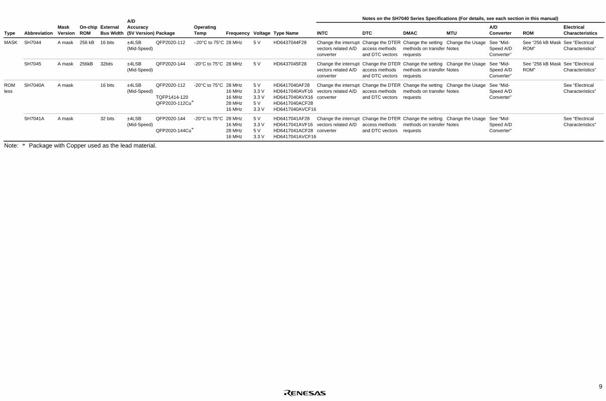
9
Type AbbreviationMaskVersion
On-chipROM
ExternalBus Width
A/DAccuracy(5V Version) Package
OperatingTemp Frequency Voltage Type Name
Notes on the SH7040 Series Specifications (For details, see each section in this manual)
A/D ElectricalINTC DTC DMAC MTU Converter ROM Characteristics
MASK SH7044 A mask 256 kB 16 bits ±4LSB(Mid-Speed)
QFP2020-112 –20°C to 75°C 28 MHz 5 V HD6437044F28 Change the interruptvectors related A/Dconverter
Change the DTERaccess methodsand DTC vectors
Change the settingmethods on transferrequests
Change the UsageNotes
See “Mid-Speed A/DConverter”
See “256 kB MaskROM”
See “ElectricalCharacteristics”
SH7045 A mask 256kB 32bits ±4LSB(Mid-Speed)
QFP2020-144 -20°C to 75°C 28 MHz 5 V HD6437045F28 Change the interruptvectors related A/Dconverter
Change the DTERaccess methodsand DTC vectors
Change the settingmethods on transferrequests
Change the UsageNotes
See “Mid-Speed A/DConverter”
See “256 kB MaskROM”
See “ElectricalCharacteristics”
ROMless
SH7040A A mask 16 bits ±4LSB(Mid-Speed)
QFP2020-112
TQFP1414-120QFP2020-112Cu*
-20°C to 75°C 28 MHz16 MHz16 MHz28 MHz16 MHz
5 V3.3 V3.3 V5 V3.3 V
HD6417040AF28HD6417040AVF16HD6417040AVX16HD6417040ACF28HD6417040AVCF16
Change the interruptvectors related A/Dconverter
Change the DTERaccess methodsand DTC vectors
Change the settingmethods on transferrequests
Change the UsageNotes
See “Mid-Speed A/DConverter”
See “ElectricalCharacteristics”
SH7041A A mask 32 bits ±4LSB(Mid-Speed)
QFP2020-144
QFP2020-144Cu*
-20°C to 75°C 28 MHz16 MHz28 MHz16 MHz
5 V3.3 V5 V3.3 V
HD6417041AF28HD6417041AVF16HD6417041ACF28HD6417041AVCF16
Change the interruptvectors related A/Dconverter
Change the DTERaccess methodsand DTC vectors
Change the settingmethods on transferrequests
Change the UsageNotes
See “Mid-Speed A/DConverter”
See “ElectricalCharacteristics”
Note: * Package with Copper used as the lead material.

10

11
1.2 Block Diagram
Figure 1.1 is a block diagram of the SH7040 Series QFP-112 pin and TQFP-120 pin. Figure 1.2 isa block diagram of the SH7040 Series QFP-144 pin.
PC15/A15
PC14/A14
PC13/A13
PC12/A12
PC11/A11
PC10/A10
PC9/A9
PC8/A8
PC7/A7
PC6/A6
PC5/A5
PC4/A4
PC3/A3
PC2/A2
PC1/A1
PC0/A0
PD15/D15
PD14/D14
PD13/D13
PD12/D12
PD11/D11
PD10/D10
PD9/D9
PD8/D8
PD7/D7
PD6/D6
PD5/D5
PD4/D4
PD3/D3
PD2/D2
PD1/D1
PD0/D0
MD3MD2MD1MD0NMI
EXTALXTAL
VCC /FWP*1
VCC
VCC
PLLVCC
PLLCAP
PLLVSS
VCCVCCVSSVSSVSSVSSVSSVSSVSSVSS
AVCCAVSS
RES/VPP*2
WDTOVF
PB
9/IR
Q7/
A21
/AD
TRG
PB
8/IR
Q6/
A20
/WA
ITP
B7/
IRQ
5/A
19/B
RE
QP
B6/
IRQ
4/A
18/B
AC
KP
B5/
IRQ
3/P
OE
3/R
DW
R
PB
4/IR
Q2/
PO
E2/
CA
SH
PB
3/IR
Q1/
PO
E1/
CA
SL
PB
2/IR
Q0/
PO
E0/
RA
SP
B1/
A17
PB
0/A
16
PA
15/C
K
PA
14/R
D
PA
13/W
RH
PA
12/W
RL
PA
11/C
S1
PA
10/C
S0
PA
9/T
CLK
D/IR
Q3
PA
8/T
CLK
C/IR
Q2
PA
7/T
CLK
B/C
S3
PA
6/T
CLK
A/C
S2
PA
5/S
CK
1/D
RE
Q1/
IRQ
1P
A4/
TX
D1
PA
3/R
XD
1
PA
2/S
CK
0/D
RE
Q0/
IRQ
0P
A1/
TX
D0
PA
0/R
XD
0
PE
15/T
IOC
4D/D
AC
K1/
IRQ
OU
TP
E14
/TIO
C4C
/DA
CK
0/A
H
PE
13/T
IOC
4B/M
RE
SP
E12
/TIO
C4A
PE
11/T
IOC
3D
PE
10/T
IOC
3C
PE
9/T
IOC
3B
PE
8/T
IOC
3A
PE
7/T
IOC
2B
PE
6/T
IOC
2A
PE
5/T
IOC
1B
PE
4/T
IOC
1A
PE
3/T
IOC
0D/D
RA
K1
PE
2/T
IOC
0C/D
RE
Q1
PE
1/T
IOC
0B/D
RA
K0
PE
0/T
IOC
0A/D
RE
Q0
: Peripheral address bus
: Peripheral data bus
: Internal address bus: Internal upper data bus: Internal lower data bus
PLL
PF
7/A
N7
PF
6/A
N6
PF
5/A
N5
PF
4/A
N4
PF
3/A
N3
PF
2/A
N2
PF
1/A
N1
PF
0/A
N0
Flash ROM/PROM/mask ROM 256kbytes/
128 kbytes/64 kbytes
RAM/cache4 kbytes/1 kbyte
CPU
Data transfercontroller
Direct memoryaccess controller
Interruptcontroller
Userbreak Bus state controller
Serial communi-cation interface(×2 channels)
Multifunction timer/pulse unit
Compare matchtimer (×2 channels)
A/Dconverter
Watch-dogtimerVSS
VSSVSS
Notes: *1 VCC in the mask and ZTAT versions; FWP in the F-ZTAT version (however, FWE in writer mode) *2 Vpp: ZTAT version only
Figure 1.1 Block Diagram of the SH7040, SH7042, SH7044 (QFP-112 Pin), SH7040, SH7042(TQFP-120 pin)
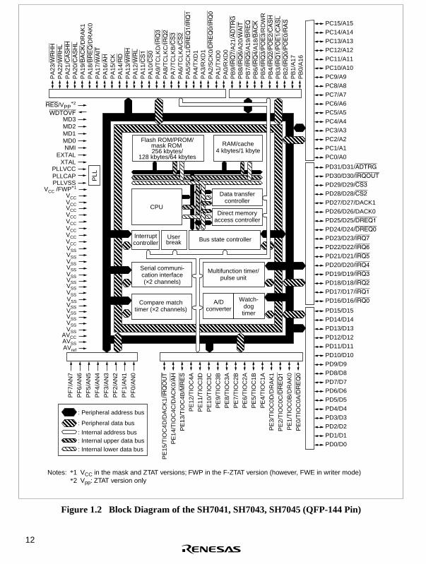
12
PC15/A15
PC14/A14
PC13/A13
PC12/A12
PC11/A11
PC10/A10
PC9/A9
PC8/A8
PC7/A7
PC6/A6
PC5/A5
PC4/A4
PC3/A3
PC2/A2
PC1/A1
PC0/A0
PD15/D15
PD14/D14
PD13/D13
PD12/D12
PD11/D11
PD10/D10
PD9/D9
PD8/D8
PD7/D7
PD6/D6
PD5/D5
PD4/D4
PD3/D3
PD2/D2
PD1/D1
PD0/D0
PD31/D31/ADTRGPD30/D30/IRQOUTPD29/D29/CS3PD28/D28/CS2PD27/D27/DACK1
PD26/D26/DACK0
PD25/D25/DREQ1PD24/D24/DREQ0PD23/D23/IRQ7PD22/D22/IRQ6PD21/D21/IRQ5PD20/D20/IRQ4PD19/D19/IRQ3PD18/D18/IRQ2PD17/D17/IRQ1PD16/D16/IRQ0
MD3MD2MD1MD0NMI
EXTALXTAL
PLLVCCPLLCAPPLLVSS
RES/VPP*2
WDTOVF
PB
9/IR
Q7/
A21
/AD
TRG
P
B8/
IRQ
6/A
20/W
AIT
PB
7/IR
Q5/
A19
/BR
EQ
PB
6/IR
Q4/
A18
/BA
CK
PB
5/IR
Q3/
PO
E3/
RD
WR
P
B4/
IRQ
2/P
OE
2/C
AS
HP
B3/
IRQ
1/P
OE
1/C
AS
LP
B2/
IRQ
0/P
OE
0/R
AS
PB
1/A
17
PB
0/A
16
PA
23/W
RH
HP
A22
/WR
HL
PA
21/C
AS
HH
P
A20
/CA
SH
LP
A19
/BA
CK
/DR
AK
1P
A18
/BR
EQ
/DR
AK
0P
A17
/WA
IT
PA
16/A
H
PA
15/C
K
PA
14/R
D
PA
13/W
RH
PA
12/W
RL
PA
11/C
S1
PA
10/C
S0
PA
9/T
CLK
D/IR
Q3
PA
8/T
CLK
C/IR
Q2
PA
7/T
CLK
B/C
S3
PA
6/T
CLK
A/C
S2
PA
5/S
CK
1/D
RE
Q1/
IRQ
1P
A4/
TX
D1
PA
3/R
XD
1P
A2/
SC
K0/
DR
EQ
0/IR
Q0
PA
1/T
XD
0P
A0/
RX
D0
PE
15/T
IOC
4D/D
AC
K1/
IRQ
OU
TP
E14
/TIO
C4C
/DA
CK
0/A
H
PE
13/T
IOC
4B/M
RE
SP
E12
/TIO
C4A
PE
11/T
IOC
3D
PE
10/T
IOC
3C
PE
9/T
IOC
3B
PE
8/T
IOC
3A
PE
7/T
IOC
2B
PE
6/T
IOC
2A
PE
5/T
IOC
1B
PE
4/T
IOC
1A
PE
3/T
IOC
0D/D
RA
K1
PE
2/T
IOC
0C/D
RE
Q1
PE
1/T
IOC
0B/D
RA
K0
PE
0/T
IOC
0A/D
RE
Q0
PLL
PF
7/A
N7
PF
6/A
N6
PF
5/A
N5
PF
4/A
N4
PF
3/A
N3
PF
2/A
N2
PF
1/A
N1
PF
0/A
N0
Flash ROM/PROM/mask ROM 256 kbytes/
128 kbytes/64 kbytes
RAM/cache4 kbytes/1 kbyte
CPU
Data transfercontroller
Direct memoryaccess controller
Interruptcontroller
Userbreak Bus state controller
Serial communi-cation interface(×2 channels)
Multifunction timer/pulse unit
Compare matchtimer (×2 channels)
A/Dconverter
Watch-dogtimer
VCC /FWP*1
VCCVCCVCCVCCVCCVCCVCCVCCVSSVSSVSSVSS
VSSVSS
VSSVSSVSS
VSSVSS
VSSVSSVSS
AVSSAVref
AVCC
: Peripheral address bus
: Peripheral data bus
: Internal address bus: Internal upper data bus: Internal lower data bus
Notes: *1 VCC in the mask and ZTAT versions; FWP in the F-ZTAT version (however, FWE in writer mode) *2 Vpp: ZTAT version only
Figure 1.2 Block Diagram of the SH7041, SH7043, SH7045 (QFP-144 Pin)

13
1.3 Pin Arrangement and Pin Functions
1.3.1 Pin Arrangment
Figure 1.3 shows the pin arrangement for the QFP-112 (top view).
PE0/TIOC0A/DREQ0PE1/TIOC0B/DRAK0PE2/TIOC0C/DREQ1PE3/TIOC0D/DRAK1
PE4/TIOC1AVSS
PF0/AN0PF1/AN1PF2/AN2PF3/AN3PF4/AN4PF5/AN5
AVSSPF6/AN6PF7/AN7
AVCCVSS
PE5/TIOC1BVCC
PE6/TIOC2APE7/TIOC2BPE8/TIOC3APE9/TIOC3B
PE10/TIOC3CVSS
PE11/TIOC3DPE12/TIOC4A
PB13/TIOC4B/MRES
858687888990919293949596979899100101102103104105106107108109110111112
56555453525150494847464544434241403938373635343332313029
RE
S/V
PP
*2
PA
15/C
KP
LLV
SS
PLL
CA
PP
LLV
CC
MD
0M
D1
VC
C (F
WP
*1)
NM
IM
D2
EX
TA
LM
D3
XT
AL
VS
SP
D0/
D0
PD
1/D
1P
D2/
D2
PD
3/D
3P
D4/
D4
VC
CP
D5/
D5
PD
6/D
6P
D7/
D7
VS
SP
D8/
D8
PD
9/D
9P
D10
/D10
PD
11/D
11
84 83 82 81 80 79 78 77 76 75 74 73 72 71 70 69 68 67 66 65 64 63 62 61 60 59 58 57 PD12/D12VSSPD13/D13PD14/D14PD15/D15PA0/RXD0PA1/TXD0PA2/SCK0/DREQ0/IRQ0PA3/RXD1PA4/TXD1PA5/SCK1/DREQ1/IRQ1
PA7/TCLKB/CS3PA8/TCLKC/IRQ2
PA10/CS0PA11/CS1VSSPA12/WRLVCCPA13/WRHWDTOVFPA14/RDVSSPB9/IRQ7/A21/ADTRGPB8/IRQ6/A20/WAITPB7/IRQ5/A19/BREQPB6/IRQ4/A18/BACK
PA6/TCLKA/CS2
PA9/TCLKD/IRQ3
1 2 3 4 5 6 7 8 9 10 11 12 13 14 15 16 17 18 19 20 21 22 23 24 25 26 27 28
PE
14/T
IOC
4C/D
AC
K0/
AH
PE
15/T
IOC
4D/D
AC
K1/
IRQ
OU
TV
SS
PC
0/A
0P
C1/
A1
PC
2/A
2P
C3/
A3
PC
4/A
4P
C5/
A5
PC
6/A
6P
C7/
A7
PC
11/A
11P
C12
/A12
PC
13/A
13P
C14
/A14
PC
15/A
15P
B0/
A16
VC
CP
B1/
A17
PB
2/IR
Q0/
PO
E0/
RA
SP
B3/
IRQ
1/P
OE
1/C
AS
LP
B4/
IRQ
2/P
OE
2/C
AS
HV
SS
PB
5/IR
Q3/
PO
E3/
RD
WR
PC
8/A
8P
C9/
A9
PC
10/A
10
VS
S
QFP-112
Notes: *1 VCC in the mask and ZTAT versions; FWP in the F-ZTAT version (however, FWE in writer mode) *2 Vpp: ZTAT version only
Figure 1.3 SH7040, SH7042, SH7044 Pin Arrangement (QFP-112 Top View)
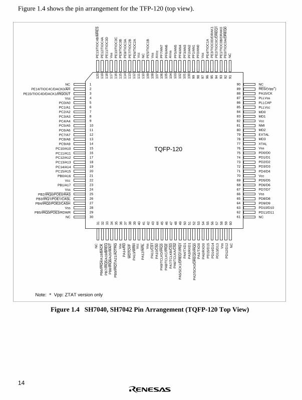
14
Figure 1.4 shows the pin arrangement for the TFP-120 (top view).
TQFP-120
PE15/TIOC4D/DACK1/IRQOUTVss
PC0/A0PC1/A1PC2/A2PC3/A3PC4/A4PC5/A5
NCPE14/TIOC4C/DACK0/AH
PC6/A6PC7/A7PC8/A8PC9/A9
PC10/A10PC11/A11PC12/A12PC13/A13
PC14/A14PC15/A15
PB0/A16Vcc
PB1/A17Vss
PB2/IRQ0/POE0/RASPB3/IRQ1/POE1/CASLPB4/IRQ2/POE2/CASH
VssPB5/IRQ3/POE3/RDWR
NC
NC
PB
6/IR
Q4/
A18
/BA
CK
PB
7/IR
Q5/
A19
/BR
EQ
PB
8/IR
Q6/
A20
/WA
ITP
B9/
IRQ
7/A
21/A
DTR
GV
ssP
A14
/RD
WD
TOV
FP
A13
/WR
HV
cc
PA
12/W
RL
Vss
PA
11/C
S1
PA
10/C
S0
PA
9/T
CLK
D/IR
Q3
PA
8/T
CLK
C/IR
Q2
PA
7/T
CLK
B/C
S3
PA
6/T
CLK
A/C
S2
PA
5/S
CK
1/D
RE
Q1/
IRQ
1P
A4/
TX
D1
PA
3/R
XD
1
PA
2/S
CK
0/D
RE
Q0/
IRQ
0P
A1/
TX
D0
PA
0/R
XD
0P
D15
/D15
PD
14/D
14P
D13
/D13 Vss
PD
12/D
12 NC
NCRES/(Vpp*)PA15/CKPLLVssPLLCAPPLLVccMD0MD1VccNMIMD2EXTALMD3
XTALVssPD0/D0PD1/D1PD2/D2PD3/D3
PD4/D4VccPD5/D5PD6/D6PD7/D7VssPD8/D8PD9/D9PD10/D10PD11/D11NC
NC
PE
13/T
IOC
4B/M
RE
SP
E12
/TIO
C4A
PE
11/T
IOC
3DV
ssP
E10
/TIO
C3C
PE
9/T
IOC
3BP
E8/
TIO
C3A
PE
7/T
IOC
2BP
E6/
TIO
C2A
Vcc
PE
5/T
IOC
1BV
ssA
Vcc
PF
7/A
N7
PF
6/A
N6
AV
ss
PF
5/A
N5
PF
4/A
N4
PF
3/A
N3
PF
2/A
N2
PF
1/A
N1
PF
0/A
N0
Vss
PE
4/T
IOC
1AP
E3/
TIO
C0D
/DR
AK
1P
E2/
TIO
C0C
/DR
EQ
1P
E1/
TIO
C0B
/DR
AK
0
NC
120
119
118
117
116
115
114
113
112
111
110
109
108
107
106
105
104
103
102
101
100
99 98 97 96 95 94 93 92 91
908988878685848382818079787776757473727170696867666564636261
123456789101112131415161718192021222324252627282930
31 32 33 34 35 36 37 38 39 40 41 42 43 44 45 46 47 48 49 50 51 52 53 54 55 56 57 58 59 60
PE
0/T
IOC
0A/D
RE
Q0
Note: * Vpp: ZTAT version only
Figure 1.4 SH7040, SH7042 Pin Arrangement (TQFP-120 Top View)

15
Figure 1.5 shows the pin arrangement for the QFP-144 (top view).
1 2 3 4 5 6 7 8 9 10 11 12 13 14 15 16 17 18 19 20 21 22 23 24 25 26 27 28
PA
23/W
RH
HP
E14
/TIO
C4C
/DA
CK
0/A
HP
A22
/WR
HL
PA
21/C
AS
HH
PE
15/T
IOC
4D/D
AC
K1/
IRQ
OU
TV
SS
PC
0/A
0P
C1/
A1
PC
2/A
2P
C3/
A3
PC
4/A
4
PC
6/A
6P
C7/
A7
PC
8/A
8P
C9/
A9
PC
10/A
10P
C11
/A11
PC
12/A
12P
C13
/A13
PC
15/A
15P
B0/
A16
VC
CP
B1/
A17
VS
S
VC
CP
C5/
A5
VS
S
PC
14/A
14
29 30 31 32 33 34 35 36
PA
20/C
AS
HL
PA
19/B
AC
K/D
RA
K1
PB
3/IR
Q1/
PO
E1/
CA
SL
PA
18/B
RE
Q/D
RA
K0
PB
4/IR
Q2/
PO
E2/
CA
SH
VS
SP
B5/
IRQ
3/P
OE
3/R
DW
R
PB
2/IR
Q0/
PO
E0/
RA
S
RE
S/V
PP
*2
PA
15/C
KP
LLV
SS
PLL
CA
PP
LLV
CC
MD
0M
D1
PA
17/W
AIT
PA
16/A
HV
CC
(FW
P*1
)N
MI
MD
2E
XT
AL
MD
3X
TA
LV
SS
PD
0/D
0P
D1/
D1
PD
2/D
2P
D3/
D3
PD
4/D
4V
SS
PD
5/D
5V
CC
PD
6/D
6P
D7/
D7
PD
8/D
8P
D9/
D9
108
107
106
105
104
103
102
101
100 99 98 94 93 92 91 90 89 88 87 85 84 83 82 8197 96 95 86
PD
10/D
10V
SS
PD
11/D
11V
CC
PD
12/D
12P
D13
/D13
PD
14/D
14P
D15
/D15
80 79 77 76 75 74 7378
7170696867666564636261605958575655545352515049484746454443424140393837
72 PD16/D16/IRQ0VSSPD17/D17/IRQ1PD18/D18/IRQ2PD19/D19/IRQ3PD20/D20/IRQ4PD21/D21/IRQ5PD22/D22/IRQ6PD23/D23/IRQ7VCCPD24/D24/DREQ0
PD27/D27/DACK1PD28/D28/CS2PD29/D29/CS3VSSPA6/TCLKA/CS2PA7/TCLKB/CS3PA8/TCLKC/IRQ2PA9/TCLKD/IRQ3
PA11/CS1PA12/WRLPA13/WRHPD30/D30/IRQOUTPD31/D31/ADTRG
VSSPD25/D25/DREQ1PD26/D26/DACK0
PA10/CS0
WDTOVFPA14/RD
PB9/IRQ7/A21/ADTRGVCCPB8/IRQ6/A20/WAITPB7/IRQ5/A19/BREQPB6/IRQ4/A18/BACK
VSS
109110111112113114115116117118119
123124125126127128129130
132133134135136
120121122
131
PE0/TIOC0A/DREQ0PE1/TIOC0B/DRAK0PE2/TIOC0C/DREQ1
VCCPE3/TIOC0D/DRAK1
PE4/TIOC1APE5/TIOC1BPE6/TIOC2A
VSSPF0/AN0PF1/AN1PF2/AN2PF3/AN3PF4/AN4PF5/AN5
AVSSPF6/AN6PF7/AN7
AVrefAVCC
VSSPA0/RXD0PA1/TXD0
PA2/SCK0/DREQ0/IRQ0PA3/RXD1PA4/TXD1
VCCPA5/SCK1/DREQ1/IRQ1
PE7/TIOC2BPE8/TIOC3APE9/TIOC3B
PE10/TIOC3CVSS
PE11/TIOC3DPE12/TIOC4A
PE13/TIOC4B/MRES
137138
140141142143144
139
QFP-144
Notes: *1 VCC in the mask and ZTAT versions; FWP in the F-ZTAT version (however, FWE in writer mode) *2 Vpp: ZTAT version only
Figure 1.5 SH7041, SH7043, SH7045 Pin Arrangement (QFP-144 Top View)

16
1.3.2 Pin Arrangement by Mode
Table 1.2 Pin Arrangement by Mode for SH7040, SH7042 (QFP-112 Pin)
Pin No. MCU Mode PROM Mode
1 PE14/TIOC4C/DACK0/AH VCC
2 PE15/TIOC4D/DACK1/IRQOUT CE
3 VSS VSS
4 PC0/A0 A0
5 PC1/A1 A1
6 PC2/A2 A2
7 PC3/A3 A3
8 PC4/A4 A4
9 PC5/A5 A5
10 PC6/A6 A6
11 PC7/A7 A7
12 PC8/A8 A8
13 PC9/A9 NC
14 PC10/A10 A10
15 PC11/A11 A11
16 PC12/A12 A12
17 PC13/A13 A13
18 PC14/A14 A14
19 PC15/A15 A15
20 PB0/A16 A16
21 VCC VCC
22 PB1/A17 NC
23 VSS VSS
24 PB2/IRQ0/POE0/RAS NC
25 PB3/IRQ1/POE1/CASL OE
26 PB4/IRQ2/POE2/CASH PGM
27 VSS VSS
28 PB5/IRQ3/POE3/RDWR VCC

17
Table 1.2 Pin Arrangement by Mode for SH7040, SH7042 (QFP-112 Pin) (cont)
Pin No. MCU Mode PROM Mode
29 PB6/IRQ4/A18/BACK NC
30 PB7/IRQ5/A19/BREQ NC
31 PB8/IRQ6/A20/WAIT NC
32 PB9/IRQ7/A21/ADTRG NC
33 VSS VSS
34 PA14/RD NC
35 WDTOVF NC
36 PA13/WRH NC
37 VCC VCC
38 PA12/WRL NC
39 VSS VSS
40 PA11/CS1 NC
41 PA10/CS0 NC
42 PA9/TCLKD/IRQ3 NC
43 PA8/TCLKC/IRQ2 NC
44 PA7/TCLKB/CS3 NC
45 PA6/TCLKA/CS2 NC
46 PA5/SCK1/DREQ1/IRQI NC
47 PA4/TXD1 NC
48 PA3 /RXD1 NC
49 PA2/SCK0/DREQ0/IRQ0 NC
50 PA1/TXD0 NC
51 PA0/RXD0 NC
52 PD15/D15 NC
53 PD14/D14 NC
54 PD13/D13 NC
55 VSS VSS
56 PD12/D12 NC
57 PD11/D11 NC
58 PD10/D10 NC

18
Table 1.2 Pin Arrangement by Mode for SH7040, SH7042 (QFP-112 Pin) (cont)
Pin No. MCU Mode PROM Mode
59 PD9/D9 NC
60 PD8/D8 NC
61 VSS VSS
62 PD7/D7 D7
63 PD6/D6 D6
64 PD5/D5 D5
65 VCC VCC
66 PD4/D4 D4
67 PD3/D3 D3
68 PD2/D2 D2
69 PD1/D1 D1
70 PD0/D0 D0
71 VSS VSS
72 XTAL NC
73 MD3 VCC
74 EXTAL VSS
75 MD2 VCC
76 NMI A9
77 VCC VCC
78 MD1 VCC
79 MD0 VCC
80 PLLVCC VCC
81 PLLCAP VSS
82 PLLVSS VSS
83 PA15/CK NC
84 RES VPP
85 PE0/TIOC0A/DREQ0 NC
86 PE1/TIOC0B/DRAK0 NC
87 PE2/TIOC0C/DREQ1 NC
88 PE3/TIOC0D/DRAK1 NC

19
Table 1.2 Pin Arrangement by Mode for SH7040, SH7042 (QFP-112 Pin) (cont)
Pin No. MCU Mode PROM Mode
89 PE4/TIOC1A NC
90 VSS VSS
91 PF0/AN0 VSS
92 PF1/AN1 VSS
93 PF2/AN2 VSS
94 PF3/AN3 VSS
95 PF4/AN4 VSS
96 PF5/AN5 VSS
97 AVSS VSS
98 PF6/AN6 VSS
99 PF7/AN7 VSS
100 AVCC VCC
101 VSS VSS
102 PE5/TIOC1B NC
103 VCC VCC
104 PE6/TIOC2A NC
105 PE7/TIOC2B NC
106 PE8/TIOC3A NC
107 PE9/TIOC3B NC
108 PE10/TIOC3C NC
109 VSS VSS
110 PE11/TIOC3D NC
111 PE12/TIOC4A NC
112 PE13/TIOC4B/MRES NC

20
Table 1.3 Pin Arrangement by Mode for SH7040, SH7042 (TQFP-120 Pin)
TQFP120 Pin No. MCU Mode PROM Mode
1 NC NC
2 PE14/TIOC4C/DACK0/AH VCC
3 PE15/TIOC4D/DACK1/IRQOUT CE
4 VSS VSS
5 PC0/A0 A0
6 PC1/A1 A1
7 PC2/A2 A2
8 PC3/A3 A3
9 PC4/A4 A4
10 PC5/A5 A5
11 PC6/A6 A6
12 PC7/A7 A7
13 PC8/A8 A8
14 PC9/A9 NC
15 PC10/A10 A10
16 PC11/A11 A11
17 PC12/A12 A12
18 PC13/A13 A13
19 PC14/A14 A14
20 PC15/A15 A15
21 PB0/A16 A16
22 VCC VCC
23 PB1/A17 NC
24 VSS VSS
25 PB2/IRQ0/POE0/RAS NC
26 PB3/IRQ1/POE1/CASL OE
27 PB4/IRQ2/POE2/CASH PGM
28 VSS VSS
29 PB5/IRQ3/POE3/RDWR VCC
30 NC NC
31 NC NC

21
Table 1.3 Pin Arrangement by Mode for SH7040, SH7042 (TQFP-120 Pin) (cont)
TQFP120 Pin No. MCU Mode PROM Mode
32 PB6/IRQ4/A18/BACK NC
33 PB7/IRQ5/A19/BREQ NC
34 PB8/IRQ6/A20/WAIT NC
35 PB9/IRQ7/A21/ADTRG NC
36 VSS VSS
37 PA14/RD NC
38 WDTOVF NC
39 PA13/WRH NC
40 VCC VCC
41 PA12/WRL NC
42 VSS VSS
43 PA11/CS1 NC
44 PA10/CS0 NC
45 PA9/TCLKD/IRQ3 NC
46 PA8/TCLKC/IRQ2 NC
47 PA7/TCLKB/CS3 NC
48 PA6/TCLKA/CS2 NC
49 PA5/SCK1/DREQ1/IRQ1 NC
50 PA4/TXD1 NC
51 PA3/RXD2 NC
52 PA2/SCK0/DREQ0/IRQ0 NC
53 PA1/TXD0 NC
54 PA0/RXD0 NC
55 PD15/D15 NC
56 PD14/D14 NC
57 PD13/D13 NC
58 VSS VSS
59 PD12/D12 NC
60 NC NC
61 NC NC
62 PD11/D11 NC

22
Table 1.3 Pin Arrangement by Mode for SH7040, SH7042 (TQFP-120 Pin) (cont)
TQFP120 Pin No. MCU Mode PROM Mode
63 PD10/D10 NC
64 PD9/D9 NC
65 PD8/D8 NC
66 VSS VSS
67 PD7/D7 D7
68 PD6/D6 D6
69 PD5/D5 D5
70 VCC VCC
71 PD4/D4 D4
72 PD3/D3 D3
73 PD2/D2 D2
74 PD1/D1 D1
75 PD0/D0 D0
76 VSS VSS
77 XTAL NC
78 MD3 VCC
79 EXTAL VSS
80 MD2 VCC
81 NMI A9
82 VCC VCC
83 MD1 VCC
84 MD0 VCC
85 PLLVCC VCC
86 PLLCAP VSS
87 PLLVSS VSS
88 PA15/CK NC
89 RES VPP
90 NC NC
91 NC NC
92 PE0/TIOC0A/DREQ0 NC
93 PE1/TIOC0B/DRAK0 NC

23
Table 1.3 Pin Arrangement by Mode for SH7040, SH7042 (TQFP-120 Pin) (cont)
TQFP120 Pin No. MCU Mode PROM Mode
94 PE2/TIOC0C/DREQ1 NC
95 PE3/TIOC0D/DRAK1 NC
96 PE4/TIOC1A NC
97 VSS VSS
98 PF0/AN0 VSS
99 PF1/AN1 VSS
100 PF2/AN2 VSS
101 PF3/AN3 VSS
102 PF4/AN4 VSS
103 PF5/AN5 VSS
104 AVSS VSS
105 PF6/AN6 VSS
106 PF7/AN7 VSS
107 AVCC VCC
108 VSS VSS
109 PE5/TIOC1B NC
110 NC NC
111 VCC VCC
112 PE6/TIOC2A NC
113 PE7/TIOC2B NC
114 PE8/TIOC3A NC
115 PE9/TIOC3B NC
116 PE10/TIOC3C NC
117 VSS VSS
118 PE11/TIOC3D NC
119 PE12/TIOC4A NC
120 PE13/TIOC4B/MRES NC

24
Table 1.4 Pin Arrangement by Mode for SH7041, SH7043 (QFP-144 Pin)
Pin No. MCU Mode PROM Mode
1 PA23/WRHH NC
2 PE14/TIOC4C/DACK0/AH VCC
3 PA22/WRHL NC
4 PA21/CASHH NC
5 PE15/TIOC4D/DACK1/IRQOUT CE
6 VSS VSS
7 PC0/A0 A0
8 PC1/A1 A1
9 PC2/A2 A2
10 PC3/A3 A3
11 PC4/A4 A4
12 VCC VCC
13 PC5/A5 A5
14 VSS VSS
15 PC6/A6 A6
16 PC7/A7 A7
17 PC8/A8 A8
18 PC9/A9 NC
19 PC10/A10 A10
20 PC11/A11 A11
21 PC12/A12 A12
22 PC13/A13 A13
23 PC14/A14 A14
24 PC15/A15 A15
25 PB0/A16 A16
26 VCC VCC
27 PB1/A17 NC
28 VSS VSS
29 PA20/CASHL NC
30 PA19/BACK/DRAK1 NC

25
Table 1.4 Pin Arrangement by Mode for SH7041, SH7043 (QFP-144 Pin) (cont)
Pin No. MCU Mode PROM Mode
31 PB2/IRQ0/POE0/RAS NC
32 PB3/IRQ1/POE1/CASL OE
33 PA18/BREQ/DRAK0 NC
34 PB4/IRQ2/POE2/CASH PGM
35 VSS VSS
36 PB5/IRQ3/POE3/RDWR VCC
37 PB6/IRQ4/A18/BACK NC
38 PB7/IRQ5/A19/BREQ NC
39 PB8/IRQ6/A20/WAIT NC
40 VCC VCC
41 PB9/IRQ7/A21/ADTRG NC
42 VSS VSS
43 PA14/RD NC
44 WDTOVF NC
45 PD31/D31/ADTRG NC
46 PD30/D30/IRQOUT NC
47 PA13/WRH NC
48 PA12/WRL NC
49 PA11/CS1 NC
50 PA10/CS0 NC
51 PA9/TCLKD/IRQ3 NC
52 PA8/TCLKC/IRQ2 NC
53 PA7/TCLKB/CS3 NC
54 PA6/TCLKA/CS2 NC
55 VSS VSS
56 PD29/D29/CS3 NC
57 PD28/D28/CS2 NC
58 PD27/D27/DACK1 NC
59 PD26/D26/DACK0 NC
60 PD25/D25/DREQ1 NC

26
Table 1.4 Pin Arrangement by Mode for SH7041, SH7043 (QFP-144 Pin) (cont)
Pin No. MCU Mode PROM Mode
61 VSS VSS
62 PD24/D24/DREQ0 NC
63 VCC VCC
64 PD23/D23/IRQ7 NC
65 PD22/D22/IRQ6 NC
66 PD21/D21/IRQ5 NC
67 PD20/D20/IRQ4 NC
68 PD19/D19/IRQ3 NC
69 PD18/D18/IRQ2 NC
70 PD17/D17/IRQ1 NC
71 VSS VSS
72 PD16/D16/IRQ0 NC
73 PD15/D15 NC
74 PD14/D14 NC
75 PD13/D13 NC
76 PD12/D12 NC
77 VCC VCC
78 PD11/D11 NC
79 VSS VSS
80 PD10/D10 NC
81 PD9/D9 NC
82 PD8/D8 NC
83 PD7/D7 D7
84 PD6/D6 D6
85 VCC VCC
86 PD5 /D5 D5
87 VSS VSS
88 PD4/D4 D4
89 PD3/D3 D3
90 PD2/D2 D2

27
Table 1.4 Pin Arrangement by Mode for SH7041, SH7043 (QFP-144 Pin) (cont)
Pin No. MCU Mode PROM Mode
91 PD1/D1 D1
92 PD0/D0 D0
93 VSS VSS
94 XTAL NC
95 MD3 VCC
96 EXTAL VSS
97 MD2 VCC
98 NMI A9
99 VCC VCC
100 PA16/AH NC
101 PA17/WAIT NC
102 MD1 VCC
103 MD0 VCC
104 PLLVCC VCC
105 PLLCAP VSS
106 PLLVSS VSS
107 PA15/CK NC
108 RES VPP
109 PE0/TIOC0A/DREQ0 NC
110 PE1/TIOC0B/DRAK0 NC
111 PE2/TIOC0C/DREQ1 NC
112 VCC VCC
113 PE3/TIOC0D/DRAK1 NC
114 PE4/TIOC1A NC
115 PE5/TIOC1B NC
116 PE6/TIOC2A NC
117 VSS VSS
118 PF0/AN0 VSS
119 PF1/AN1 VSS
120 PF2/AN2 VSS
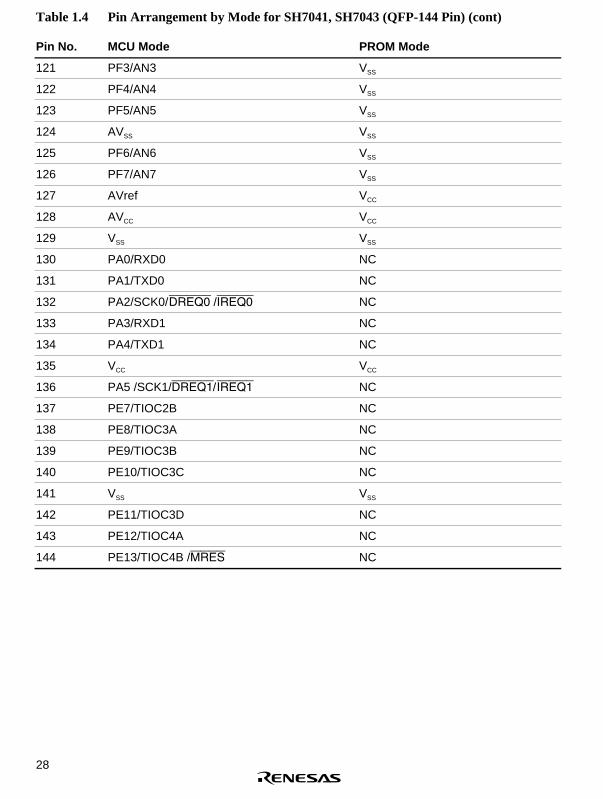
28
Table 1.4 Pin Arrangement by Mode for SH7041, SH7043 (QFP-144 Pin) (cont)
Pin No. MCU Mode PROM Mode
121 PF3/AN3 VSS
122 PF4/AN4 VSS
123 PF5/AN5 VSS
124 AVSS VSS
125 PF6/AN6 VSS
126 PF7/AN7 VSS
127 AVref VCC
128 AVCC VCC
129 VSS VSS
130 PA0/RXD0 NC
131 PA1/TXD0 NC
132 PA2/SCK0/DREQ0 /IREQ0 NC
133 PA3/RXD1 NC
134 PA4/TXD1 NC
135 VCC VCC
136 PA5 /SCK1/DREQ1/IREQ1 NC
137 PE7/TIOC2B NC
138 PE8/TIOC3A NC
139 PE9/TIOC3B NC
140 PE10/TIOC3C NC
141 VSS VSS
142 PE11/TIOC3D NC
143 PE12/TIOC4A NC
144 PE13/TIOC4B /MRES NC

29
Table 1.5 Pin Arrangement by Mode for SH7044 (QFP-112 Pin)
PinNo. MCU Writer mode
1 PE14/TIOC4C/DACK0/AH NC
2 PE15/TIOC4D/DACK1/IRQOUT NC
3 VSS VSS
4 PC0/A0 A0
5 PC1/A1 A1
6 PC2/A2 A2
7 PC3/A3 A3
8 PC4/A4 A4
9 PC5/A5 A5
10 PC6/A6 A6
11 PC7/A7 A7
12 PC8/A8 A8
13 PC9/A9 A9
14 PC10/A10 A10
15 PC11/A11 A11
16 PC12/A12 A12
17 PC13/A13 A13
18 PC14/A14 A14
19 PC15/A15 A15
20 PB0/A16 A16
21 VCC VCC
22 PB1/A17 NC
23 VSS VSS
24 PB2/IRQ0/POE0/RAS NC
25 PB3/IRQ1/POE1/CASL NC
26 PB4/IRQ2/POE2/CASH A17
27 VSS VSS
28 PB5/IRQ3/POE3/RDWR NC
29 PB6/IRQ4/A18/BACK NC
30 PB7/IRQ5/A19/BREQ NC
31 PB8/IRQ6/A20/WAIT NC
32 PB9/IRQ7/A21/ADTRG NC

30
Table 1.5 Pin Arrangement by Mode for SH7044 (QFP-112 Pin) (cont)
PinNo. MCU Writer mode
33 VSS VSS
34 PA14/RD NC
35 WDTOVF NC
36 PA13/WRH NC
37 VCC VCC
38 PA12/WRL NC
39 VSS VSS
40 PA11/CS1 NC
41 PA10/CS0 NC
42 PA9/TCLKD/IRQ3 CE
43 PA8/TCLKC/IRQ2 OE
44 PA7/TCLKB/CS3 WE
45 PA6/TCLKA/CS2 NC
46 PA5/SCK1/DREQ1/IRQ1 VCC
47 PA4/TXD1 NC
48 PA3/RXD1 NC
49 PA2/SCK0/DREQ0/IRQ0 VCC
50 PA1/TXD0 VCC
51 PA0/RXD0 NC
52 PD15/D15 NC
53 PD14/D14 NC
54 PD13/D13 NC
55 VSS VSS
56 PD12/D12 NC
57 PD11/D11 NC
58 PD10/D10 NC
59 PD9/D9 NC
60 PD8/D8 NC
61 VSS VSS
62 PD7/D7 D7
63 PD6/D6 D6
64 PD5/D5 D5
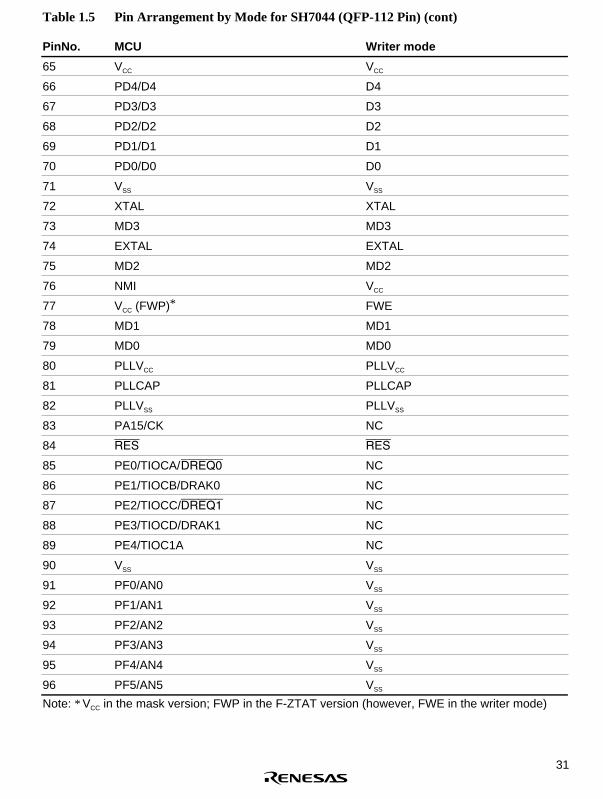
31
Table 1.5 Pin Arrangement by Mode for SH7044 (QFP-112 Pin) (cont)
PinNo. MCU Writer mode
65 VCC VCC
66 PD4/D4 D4
67 PD3/D3 D3
68 PD2/D2 D2
69 PD1/D1 D1
70 PD0/D0 D0
71 VSS VSS
72 XTAL XTAL
73 MD3 MD3
74 EXTAL EXTAL
75 MD2 MD2
76 NMI VCC
77 VCC (FWP)* FWE
78 MD1 MD1
79 MD0 MD0
80 PLLVCC PLLVCC
81 PLLCAP PLLCAP
82 PLLVSS PLLVSS
83 PA15/CK NC
84 RES RES
85 PE0/TIOCA/DREQ0 NC
86 PE1/TIOCB/DRAK0 NC
87 PE2/TIOCC/DREQ1 NC
88 PE3/TIOCD/DRAK1 NC
89 PE4/TIOC1A NC
90 VSS VSS
91 PF0/AN0 VSS
92 PF1/AN1 VSS
93 PF2/AN2 VSS
94 PF3/AN3 VSS
95 PF4/AN4 VSS
96 PF5/AN5 VSS
Note: * VCC in the mask version; FWP in the F-ZTAT version (however, FWE in the writer mode)

32
Table 1.5 Pin Arrangement by Mode for SH7044 (QFP-112 Pin) (cont)
PinNo. MCU Writer mode
97 AVSS VSS
98 PF6/AN6 VSS
99 PF7/AN7 VSS
100 AVCC VCC
101 VSS VSS
102 PE5/TIOC1B NC
103 VCC VCC
104 PE6/TIOC2A NC
105 PE7/TIOC2B NC
106 PE8/TIOC3A NC
107 PE9/TIOC3B NC
108 PE10/TIOC3C NC
109 VSS VSS
110 PE11/TIOC3D NC
111 PE12/TIOC4A NC
112 PE13/TIOC4B/MRES NC

33
Table 1.6 Pin Arrangement by Mode for SH7045 (QFP-144 Pin)
PinNo. MCU Writer mode
1 PA23/WRHH NC
2 PE14/TIOC4C/DACK0/AH NC
3 PA22/WRHL NC
4 PA21/CASHH NC
5 PE15/TIOC4D/DACK1/IRQOUT NC
6 VSS VSS
7 PC0/A0 A0
8 PC1/A1 A1
9 PC2/A2 A2
10 PC3/A3 A3
11 PC4/A4 A4
12 VCC VCC
13 PC5/A5 A5
14 VSS VSS
15 PC6/A6 A6
16 PC7/A7 A7
17 PC8/A8 A8
18 PC9/A9 A9
19 PC10/A10 A10
20 PC11/A11 A11
21 PC12/A12 A12
22 PC13/A13 A13
23 PC14/A14 A14
24 PC15/A15 A15
25 PB0/A16 A16
26 VCC VCC
27 PB1/A17 NC
28 VSS VSS
29 PA20/CASHL NC
30 PA19/BACK/DRAK1 NC
31 PB2/IRQ0/POE0/RAS NC
32 PB3/IRQ1/POE1/CASL NC
33 PA18/BREQ/DRAK0 NC
34 PB4/IRQ2/POE2/CASH A17
35 VSS VSS
36 PB5/IRQ3/POE3/RDWR NC

34
Table 1.6 Pin Arrangement by Mode for SH7045 (QFP-144 Pin) (cont)
PinNo. MCU Writer mode
37 PB6/IRQ4/A18/BACK NC
38 PB7/IRQ5/A19/BREQ NC
39 PB8/IRQ6/A20/WAIT NC
40 VCC VCC
41 PB9/IRQ7/A21/ADTRG NC
42 VSS VSS
43 PA14/RD NC
44 WDTOVF NC
45 PD31/D31/ADTRG NC
46 PD30/D30/IRQOUT NC
47 PA13/WRH NC
48 PA12/WRL NC
49 PA11/CS1 NC
50 PA10/CS0 NC
51 PA9/TCLKD/IRQ3 CE52 PA8/TCLKC/IRQ2 OE53 PA7/TCLKB/CS3 WE54 PA6/TCLKA/CS2 NC
55 VSS VSS
56 PD29/D29/CS3 NC
57 PD28/D28/CS2 NC
58 PD27/D27/DACK1 NC
59 PD26/D26/DACK0 NC
60 PD25/D25/DREQ1 NC
61 VSS VSS
62 PD24/D24/DREQ0 NC
63 VCC VCC
64 PD23/D23/IRQ7 NC
65 PD22/D22/IRQ6 NC
66 PD21/D21/IRQ5 NC
67 PD20/D20/IRQ4 NC
68 PD19/D19/IRQ3 NC
69 PD18/D18/IRQ2 NC
70 PD17/D17/IRQ1 NC
71 VSS VSS
72 PD16/D16/IRQ0 NC

35
Table 1.6 Pin Arrangement by Mode for SH7045 (QFP-144 Pin) (cont)
PinNo. MCU Writer mode
73 PD15/D15 NC
74 PD14/D14 NC
75 PD13/D13 NC
76 PD12/D12 NC
77 VCC VCC
78 PD11/D11 NC
79 VSS VSS
80 PD10/D10 NC
81 PD9/D9 NC
82 PD8/D8 NC
83 PD7/D7 D7
84 PD6/D6 D6
85 VCC VCC
86 PD5/D5 D5
87 VSS VSS
88 PD4/D4 D4
89 PD3/D3 D3
90 PD2/D2 D2
91 PD1/D1 D1
92 PD0/D0 D0
93 VSS VSS
94 XTAL XTAL
95 MD3 MD3
96 EXTAL EXTAL
97 MD2 MD2
98 NMI VCC
99 VCC (FWP)* FWE
100 PA16/AH NC
101 PA17/WAIT NC
102 MD1 MD1
103 MD0 MD0
104 PLLVCC PLLVCC
105 PLLCAP PLLCAP
106 PLLVSS PLLVSS
107 PA15/CK NC Note: * VCC in the mask version; FWP in the F-ZTAT version (however, FWE in the writer mode)

36
Table 1.6 Pin Arrangement by Mode for SH7045 (QFP-144 Pin) (cont)
PinNo. MCU Writer mode
108 RES RES109 PE0/TIOC0A/DREQ0 NC
110 PE1/TIOC0B/DRAK0 NC
111 PE2/TIOC0C/DREQ1 NC
112 VCC VCC
113 PE3/TIOC0D/DRAK1 NC
114 PE4/TIOC1A NC
115 PE5/TIOC1B NC
116 PE6/TIOC2A NC
117 VSS VSS
118 PF0/AN0 VSS
119 PF1/AN1 VSS
120 PF2/AN2 VSS
121 PF3/AN3 VSS
122 PF4/AN4 VSS
123 PF5/AN5 VSS
124 AVSS VSS
125 PF6/AN6 VSS
126 PF7/AN7 VSS
127 AVref VCC
128 AVCC VCC
129 VSS VSS
130 PA0/RXD0 NC
131 PA1/TXD0 VCC
132 PA2/SCK0/DREQ0/IRQ0 VCC
133 PA3/RXD1 NC
134 PA4/TXD1 NC
135 VCC VCC
136 PA5/SCK1/DREQ1/IRQ1 VCC
137 PE7/TIOC2B NC
138 PE8/TIOC3A NC
139 PE9/TIOC3B NC
140 PE10/TIOC3C NC
141 VSS VSS
142 PE11/TIOC3D NC
143 PE12/TIOC4A NC
144 PE13/TIOC4B/MRES NC
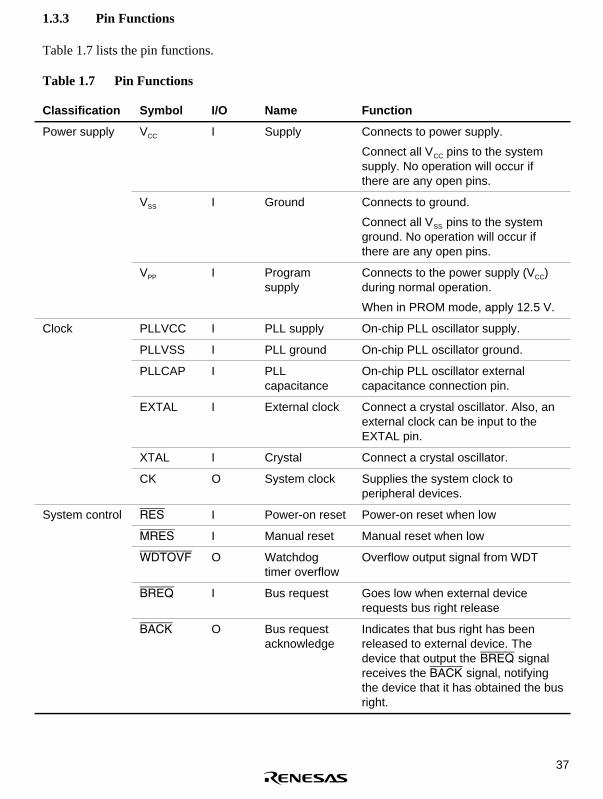
37
1.3.3 Pin Functions
Table 1.7 lists the pin functions.
Table 1.7 Pin Functions
Classification Symbol I/O Name Function
Power supply VCC I Supply Connects to power supply.
Connect all VCC pins to the systemsupply. No operation will occur ifthere are any open pins.
VSS I Ground Connects to ground.
Connect all VSS pins to the systemground. No operation will occur ifthere are any open pins.
VPP I Programsupply
Connects to the power supply (VCC)during normal operation.
When in PROM mode, apply 12.5 V.
Clock PLLVCC I PLL supply On-chip PLL oscillator supply.
PLLVSS I PLL ground On-chip PLL oscillator ground.
PLLCAP I PLLcapacitance
On-chip PLL oscillator externalcapacitance connection pin.
EXTAL I External clock Connect a crystal oscillator. Also, anexternal clock can be input to theEXTAL pin.
XTAL I Crystal Connect a crystal oscillator.
CK O System clock Supplies the system clock toperipheral devices.
System control RES I Power-on reset Power-on reset when low
MRES I Manual reset Manual reset when low
WDTOVF O Watchdogtimer overflow
Overflow output signal from WDT
BREQ I Bus request Goes low when external devicerequests bus right release
BACK O Bus requestacknowledge
Indicates that bus right has beenreleased to external device. Thedevice that output the BREQ signalreceives the BACK signal, notifyingthe device that it has obtained the busright.

38
Table 1.7 Pin Functions (cont)
Classification Symbol I/O Name Function
Operatingmode control
MD0–MD3 I Mode set Determines the operating mode. Donot change input value duringoperation.
FWP I Flash memorywrite protect
Protects flash memory from beingwritten or deleted.
Interrupts NMI I Non-maskableinterrupt
Non-maskable interrupt request pin.Enables selection of whether toaccept on the rising or falling edge.
IRQ0–IRQ7
I Interruptrequests 0–7
Maskable interrupt request pins.Allows selection of level input andedge input.
IRQOUT O Interrupt requestoutput
Indicates that interrupt cause hasoccurred. Enables notification ofinterrupt generation also during busrelease.
Address bus A0–A21 O Address bus Outputs addresses.
Data bus D0–D15(QFP-112)
D0–D31(QFP-144)
I/O Data bus 16-bit (QFP-112 pin and TQFP-120pin versions) or 32-bit (QFP-144 pinversion) bidirectional data bus.
Bus control CS0–CS3 O Chip selects 0–3 Chip select signals for externalmemory or devices.
RD O Read Indicates reading from an externaldevice.
WRH O Upper write Indicates writing the upper 8 bits(15–8) of external data.
WRL O Lower write Indicates writing the lower 8 bits(7–0) of external data.
WAIT I Wait Input causes insertion of wait cyclesinto the bus cycle during externalspace access.
RAS O Row addressstrobe
Timing signal for DRAM rowaddress strobe.
CASH O Upper columnaddress strobe
Timing signal for DRAM columnaddress strobe.
Output when the upper 8 bits ofdata are accessed.

39
Table 1.7 Pin Functions (cont)
Classification Symbol I/O Name Function
Bus control(cont)
CASL O Lower columnaddress strobe
Timing signal for DRAM columnaddress strobe.
Output when the lower 8 bits ofdata are accessed.
RDWR O DRAMread/write
DRAM write strobe signal.
AH O Address hold Address hold timing signal fordevices using an address/datamultiplex bus.
WRHH(QFP-144)
O HH write Indicates the writing of bits 31 to24 of external data.
WRHL(QFP-144)
O HL write Indicates the writing of bits 23 to16 of external data.
CASHH(QFP-144)
O HH columnaddress strobe
Timing signal for DRAM columnaddress strobe. Output when bits31 to 24 of data are accessed.
CASHL(QFP-144)
O HL columnaddress strobe
Timing signal for DRAM columnaddress strobe. Output when bits23 to 16 of data are accessed.
Bus controlmultifunctiontimer/pulse unit
TCLKA
TCLKB
TCLKC
TCLKD
I MTU timerclock input
Input pins for external clocks tothe MTU counter.
TIOC0A
TIOC0B
TIOC0C
TIOC0D
I/O MTU inputcapture/ outputcompare(channel 0)
Channel 0 input captureinput/output compare output/PWMoutput pins.
TIOC1A
TIOC1B
I/O MTU inputcapture/outputcompare(channel 1)
Channel 1 input captureinput/output compare output/PWMoutput pins.
TIOC2A
TIOC2B
I/O MTU inputcapture/outputcompare(channel 2)
Channel 2 input captureinput/output compare output/PWMoutput pins.

40
Table 1.7 Pin Functions (cont)
Classification Symbol I/O Name Function
Bus controlmultifunctiontimer/pulse unit(cont)
TIOC3A
TIOC3B
TIOC3C
TIOC3D
I/O MTU inputcapture/outputcompare(channel 3)
Channel 3 input capture input/outputcompare output/PWM output pins.
TIOC4A
TIOC4B
TIOC4C
TIOC4D
I/O MTU inputcapture/outputcompare(channel 4)
Channel 4 input capture input/outputcompare output/PWM output pins.
Direct memoryaccesscontroller(DMAC)
DREQ0–DREQ1
I DMA transferrequest(channels 0, 1)
Input pin for external requests forDMA transfer.
DRAK0–DRAK1
O DREQ requestacknowledgment(channels 0, 1)
Output the input samplingacknowledgment of external DMAtransfer requests.
DACK0–DACK1
O DMA transferstrobe (channels0, 1)
Output a strobe to the external I/O ofexternal DMA transfer requests.
Serialcommunicationinterface (SCI)
TxD0–TxD1
O Transmit data(channels 0, 1)
SCI0, SCI1 transmit data output pins.(TxD1 is used for data transfer duringboot mode of F-ZTAT)
RxD0–RxD1
I Receive data(channels 0, 1)
SCI0, SCI1 receive data input pins.(RxD1 is used for data transfer duringboot mode of F-ZTAT)
SCK0–SCK1
I/O Serial clock(channels 0, 1)
SCI0, SCI1 clock input/output pins.
A/D Converter AVCC I Analog supply Analog supply; connected to VCC.
AVSS I Analog ground Analog supply; connected to VSS.
AVref(QFP-144only)
I Analog referencesupply
Analog reference supply input pin.(Connected to AVCC internally inQFP-112 and TQFP-120.)
AN0–AN7 I Analog input Analog signal input pins.
ADTRG I A/D conversiontrigger input
External trigger input for A/Dconversion start.

41
Table 1.7 Pin Functions (cont)
Classification Symbol I/O Name Function
I/O ports POE0–POE3
I Port outputenable
Input pin for port pin drive controlwhen general use ports areestablished as output.
PA0–PA15(QFP-112)
PA0–PA23(QFP-144)
I/O General purposeport
General purpose input/output portpins.
Each bit can be designated forinput/output.
PB0–PB9 I/O General purposeport
General purpose input/output portpins.
Each bit can be designated forinput/output.
PC0–PC15
I/O General purposeport
General purpose input/output portpins.
Each bit can be designated forinput/output.
PD0–PD15(QFP-112)
PD0–PD31(QFP-144)
I/O General purposeport
General purpose input/output portpins.
Each bit can be designated forinput/output.
PE0–PE15
I/O General purposeport
General purpose input/output portpins.
Each bit can be designated forinput/output.
PF0–PF7 I General purposeport
General purpose input port pins.
Usage Notes
1. Unused input pins should be pulled up or pulled down.
2. The WDTOVF pin should not be pulled down in the SH7044/SH7045 F-ZTAT version.However, if it is necessary to pull this pin down, a resistance of 100 kΩ or higher should beused.

42
1.4 The F-ZTAT Version Onboard Programming
There are 2 modes on the F-ZTAT version: a mode that writes and overwrites programs using thespecial writer and a mode that writes and overwrites programs onboard the application system.
When rebooting after setting each mode pin and FWP pin during the reset condition, themicrocomputer will transfer to one of the modes indicated in figure 1.6. In the user mode, data canbe read from the flash memory but cannot be written or deleted. Use the boot mode and the userprogram mode to write to the flash memory or delete data.
In the boot mode, SCI1 (TXD1, RXD1) is used for data transfer. It is possible to automaticallyadjust the transfer bit rate to the transfer bit rate of the host.
Table 1.8 Pins during the Onboard Programming Mode
Notation I/O Function
FWP Input Hardware protected flash memory write/delete
MD1 Input User programming mode/boot mode setting
MD2 Input Clock mode (PLL) setting
MD3 Input Clock mode (PLL) setting
TxD1 Output Serial sent data output
RxD1 Input Serial receive data input
User mode
Power-on reset condition
User program
mode
Boot mode
Onboard programming mode
*
*
FWP=1
MD1=1, FWP=1
RES=0
MD1=
1, F
WP=0
RES=0
FWP=0 MD
1=1,
FW
P=
0
RE
S=
0
Notes: For transferring between user mode and user program mode, proceed while CPU is not programming or erasing the flash memory.* RAM emulation permitted
Figure 1.6 Condition Transfer for Flash Memory

43
<Host>
Write control program
Write control program area
Boot program area
Application program
Application program
<SH7044/45> RXD1 TXD1
Boot program
<Flash memory> <RAM>
SCI 1
Figure. 1.7 Data Transfer during Boot Mode

44

45
Section 2 CPU
2.1 Register Configuration
The register set consists of sixteen 32-bit general registers, three 32-bit control registers and four32-bit system registers.
2.1.1 General Registers (Rn)
The sixteen 32-bit general registers (Rn) are numbered R0–R15. General registers are used fordata processing and address calculation. R0 is also used as an index register. Several instructionshave R0 fixed as their only usable register. R15 is used as the hardware stack pointer (SP). Savingand recovering the status register (SR) and program counter (PC) in exception processing isaccomplished by referencing the stack using R15. Figure 2.1 shows the general registers.
R0*1
R1
R2
R3
R4
R5
R6
R7
R8
R9
R10
R11
R12
R13
R14R15, SP (hardware stack pointer)*2
031
*1
*2
R0 functions as an index register in the indirect indexed register addressing mode and indirect indexed GBR addressing mode. In some instructions, R0 functions as a fixed source register or destination register.R15 functions as a hardware stack pointer (SP) during exception processing.
Notes:
Figure 2.1 General Registers

46
2.1.2 Control Registers
The 32-bit control registers consist of the 32-bit status register (SR), global base register (GBR),and vector base register (VBR). The status register indicates processing states. The global baseregister functions as a base address for the indirect GBR addressing mode to transfer data to theregisters of on-chip peripheral modules. The vector base register functions as the base address ofthe exception processing vector area (including interrupts). Figure 2.2 shows a control register.
9 8 7 6 5 4 3 2 1 0
M QI3 I2 I1 I0 S T
0
031
31
GBR
VBR
SR
31
S bit: Used by the MAC instruction.
Reserved bits. This bit always read 0. The write value should always be 0.
Reserved bits. 0 is read. Write only.
Bits I0–I3: Interrupt mask bits.
M and Q bits: Used by the DIV0U, DIV0S,and DIV1 instructions.
Global base register (GBR):Indicates the base address of the indirect GBR addressing mode. The indirect GBR addressing mode is used in data transferfor on-chip peripheral modules registerareas and in logic operations.
Vector base register (VBR):Stores the base address of the exceptionprocessing vector area.
SR: Status register
T bit: The MOVT, CMP/cond, TAS, TST, BT (BT/S), BF (BF/S), SETT, and CLRTinstructions use the T bit to indicate true(1) or false (0). The ADDV, ADDC,SUBV, SUBC, DIV0U, DIV0S, DIV1,NEGC, SHAR, SHAL, SHLR, SHLL,ROTR, ROTL, ROTCR, and ROTCLinstructions also use the T bit to indicatecarry/borrow or overflow/underflow.
Figure 2.2 Control Registers

47
2.1.3 System Registers
System registers consist of four 32-bit registers: high and low multiply and accumulate registers(MACH and MACL), the procedure register (PR), and the program counter (PC). The multiplyand accumulate registers store the results of multiply and accumulate operations. The procedureregister stores the return address from the subroutine procedure. The program counter storesprogram addresses to control the flow of the processing. Figure 2.3 shows a system register.
MACL
PR
PC
MACH
31 0
0
0
31
31
Multiply and accumulate (MAC)registers high and low (MACH, MACL): Stores the results of multiply and accumulate operations.
Procedure register (PR): Stores a return address from a subroutine procedure.
Program counter (PC): Indicates the fourth byte (second instruction) after the current instruction.
Figure 2.3 System Registers
2.1.4 Initial Values of Registers
Table 2.1 lists the values of the registers after reset.
Table 2.1 Initial Values of Registers
Classification Register Initial Value
General registers R0–R14 Undefined
R15 (SP) Value of the stack pointer in the vector address table
Control registers SR Bits I3–I0 are 1111 (H'F), reserved bits are 0, and otherbits are undefined
GBR Undefined
VBR H'00000000
System registers MACH, MACL, PR Undefined
PC Value of the program counter in the vector address table

48
2.2 Data Formats
2.2.1 Data Format in Registers
Register operands are always longwords (32 bits). When the memory operand is only a byte (8bits) or a word (16 bits), it is sign-extended into a longword when loaded into a register (figure2.4).
31 0Longword
Figure 2.4 Longword Operand
2.2.2 Data Format in Memory
Memory data formats are classified into bytes, words, and longwords. Byte data can be accessedfrom any address, but an address error will occur if you try to access word data starting from anaddress other than 2n or longword data starting from an address other than 4n. In such cases, thedata accessed cannot be guaranteed. The hardware stack area, referred to by the hardware stackpointer (SP, R15), uses only longword data starting from address 4n because this area holds theprogram counter and status register (figure 2.5).
31 01523 7
Byte Byte Byte Byte
WordWordAddress 2n
Address 4n Longword
Address m Address m + 2
Address m + 1 Address m + 3
Figure 2.5 Byte, Word, and Longword Alignment
2.2.3 Immediate Data Format
Byte (8-bit) immediate data resides in an instruction code. Immediate data accessed by the MOV,ADD, and CMP/EQ instructions is sign-extended and handled in registers as longword data.Immediate data accessed by the TST, AND, OR, and XOR instructions is zero-extended andhandled as longword data. Consequently, AND instructions with immediate data always clear theupper 24-bits of the destination register.
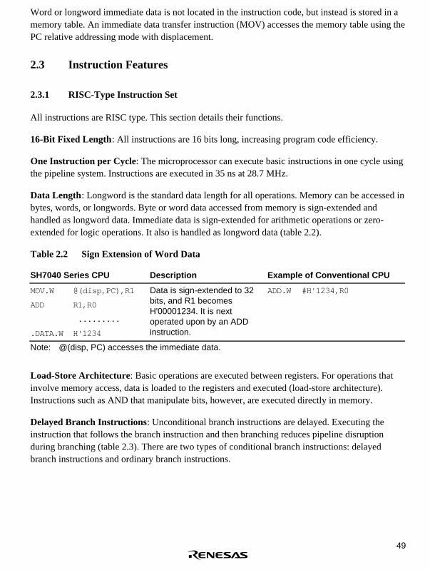
49
Word or longword immediate data is not located in the instruction code, but instead is stored in amemory table. An immediate data transfer instruction (MOV) accesses the memory table using thePC relative addressing mode with displacement.
2.3 Instruction Features
2.3.1 RISC-Type Instruction Set
All instructions are RISC type. This section details their functions.
16-Bit Fixed Length: All instructions are 16 bits long, increasing program code efficiency.
One Instruction per Cycle: The microprocessor can execute basic instructions in one cycle usingthe pipeline system. Instructions are executed in 35 ns at 28.7 MHz.
Data Length: Longword is the standard data length for all operations. Memory can be accessed inbytes, words, or longwords. Byte or word data accessed from memory is sign-extended andhandled as longword data. Immediate data is sign-extended for arithmetic operations or zero-extended for logic operations. It also is handled as longword data (table 2.2).
Table 2.2 Sign Extension of Word Data
SH7040 Series CPU Description Example of Conventional CPU
MOV.W @(disp,PC),R1
ADD R1,R0
.........
.DATA.W H'1234
Data is sign-extended to 32bits, and R1 becomesH'00001234. It is nextoperated upon by an ADDinstruction.
ADD.W #H'1234,R0
Note: @(disp, PC) accesses the immediate data.
Load-Store Architecture: Basic operations are executed between registers. For operations thatinvolve memory access, data is loaded to the registers and executed (load-store architecture).Instructions such as AND that manipulate bits, however, are executed directly in memory.
Delayed Branch Instructions: Unconditional branch instructions are delayed. Executing theinstruction that follows the branch instruction and then branching reduces pipeline disruptionduring branching (table 2.3). There are two types of conditional branch instructions: delayedbranch instructions and ordinary branch instructions.

50
Table 2.3 Delayed Branch Instructions
SH7040 Series CPU Description Example of Conventional CPU
BRA TRGET
ADD R1,R0
Executes an ADD beforebranching to TRGET
ADD.W R1,R0
BRA TRGET
Multiplication/Accumulation Operation : 16-bit × 16-bit → 32-bit multiplication operations areexecuted in one to two cycles. 16-bit × 16-bit + 64-bit → 64-bit multiplication/accumulationoperations are executed in two to three cycles. 32-bit × 32-bit → 64-bit and 32-bit × 32-bit + 64-bit → 64-bit multiplication/accumulation operations are executed in two to four cycles.
T Bit : The T bit in the status register changes according to the result of the comparison, and inturn is the condition (true/false) that determines if the program will branch. The number ofinstructions that change the T bit is kept to a minimum to improve the processing speed (table2.4).
Table 2.4 T Bit
SH7040 Series CPU Description Example of Conventional CPU
CMP/GE R1,R0
BT TRGET0
BF TRGET1
T bit is set when R0 ≥ R1. Theprogram branches to TRGET0when R0 ≥ R1 and to TRGET1when R0 < R1.
CMP.W R1,R0
BGE TRGET0
BLT TRGET1
ADD #1,R0
CMP/EQ #0,R0
BT TRGET
T bit is not changed by ADD. T bit isset when R0 = 0. The programbranches if R0 = 0.
SUB.W #1,R0
BEQ TRGET
Immediate Data: Byte (8-bit) immediate data resides in instruction code. Word or longwordimmediate data is not input via instruction codes but is stored in a memory table. An immediatedata transfer instruction (MOV) accesses the memory table using the PC relative addressing modewith displacement (table 2.5).

51
Table 2.5 Immediate Data Accessing
Classification SH7040 Series CPU Example of Conventional CPU
8-bit immediate MOV #H'12,R0 MOV.B #H'12,R0
16-bit immediate MOV.W @(disp,PC),R0
.................
.DATA.W H'1234
MOV.W #H'1234,R0
32-bit immediate MOV.L @(disp,PC),R0
.................
.DATA.L H'12345678
MOV.L #H'12345678,R0
Note: @(disp, PC) accesses the immediate data.
Absolute Address: When data is accessed by absolute address, the value already in the absoluteaddress is placed in the memory table. Loading the immediate data when the instruction isexecuted transfers that value to the register and the data is accessed in the indirect registeraddressing mode (table 2.6).
Table 2.6 Absolute Address Accessing
Classification SH7040 Series CPU Example of Conventional CPU
Absolute address MOV.L @(disp,PC),R1
MOV.B @R1,R0
..................
.DATA.L H'12345678
MOV.B @H'12345678,R0
Note: @(disp,PC) accesses the immediate data.
16-Bit/32-Bit Displacement: When data is accessed by 16-bit or 32-bit displacement, the pre-existing displacement value is placed in the memory table. Loading the immediate data when theinstruction is executed transfers that value to the register and the data is accessed in the indirectindexed register addressing mode (table 2.7).
Table 2.7 Displacement Accessing
Classification SH7040 Series CPU Example of Conventional CPU
16-bit displacement MOV.W @(disp,PC),R0
MOV.W @(R0,R1),R2
..................
.DATA.W H'1234
MOV.W @(H'1234,R1),R2
Note: @(disp,PC) accesses the immediate data.

52
2.3.2 Addressing Modes
Table 2.8 describes addressing modes and effective address calculation.
Table 2.8 Addressing Modes and Effective Addresses
AddressingMode
InstructionFormat Effective Addresses Calculation Equation
Direct registeraddressing
Rn The effective address is register Rn. (The operandis the contents of register Rn.)
—
Indirect registeraddressing
@Rn The effective address is the content of register Rn.
Rn Rn
Rn
Post-incrementindirect registeraddressing
@Rn+ The effective address is the content of register Rn.A constant is added to the content of Rn after theinstruction is executed. 1 is added for a byteoperation, 2 for a word operation, and 4 for alongword operation.
Rn Rn
1/2/4
+Rn + 1/2/4
Rn
(After theinstructionexecutes)
Byte: Rn + 1→ Rn
Word: Rn + 2→ Rn
Longword:Rn + 4 → Rn
Pre-decrementindirect registeraddressing
@–Rn The effective address is the value obtained bysubtracting a constant from Rn. 1 is subtracted fora byte operation, 2 for a word operation, and 4 fora longword operation.
Rn
1/2/4
Rn – 1/2/4–Rn – 1/2/4
Byte: Rn – 1→ Rn
Word: Rn – 2→ Rn
Longword:Rn – 4 → Rn(Instructionexecuted withRn aftercalculation)

53
Table 2.8 Addressing Modes and Effective Addresses (cont)
AddressingMode
InstructionFormat Effective Addresses Calculation Equation
Indirect registeraddressing withdisplacement
@(disp:4,Rn)
The effective address is Rn plus a 4-bitdisplacement (disp). The value of disp is zero-extended, and remains the same for a byteoperation, is doubled for a word operation, and isquadrupled for a longword operation.
Rn
Rn + disp × 1/2/4+
×
1/2/4
disp(zero-extended)
Byte: Rn +disp
Word: Rn +disp × 2
Longword: Rn+ disp × 4
Indirect indexedregisteraddressing
@(R0, Rn) The effective address is the Rn value plus R0.
Rn
R0
Rn + R0+
Rn + R0
Indirect GBRaddressing withdisplacement
@(disp:8,GBR)
The effective address is the GBR value plus an8-bit displacement (disp). The value of disp is zero-extended, and remains the same for a byte opera-tion, is doubled for a word operation, and isquadrupled for a longword operation.
GBR
1/2/4
GBR+ disp × 1/2/4
+
×
disp(zero-extended)
Byte: GBR +disp
Word: GBR +disp × 2
Longword:GBR + disp ×4

54
Table 2.8 Addressing Modes and Effective Addresses (cont)
AddressingMode
InstructionFormat Effective Addresses Calculation Equation
Indirect indexedGBR addressing
@(R0, GBR) The effective address is the GBR value plus the R0.
GBR
R0
GBR + R0+
GBR + R0
PC relativeaddressing withdisplacement
@(disp:8,PC)
The effective address is the PC value plus an 8-bitdisplacement (disp). The value of disp is zero-extended, and is doubled for a word operation, andquadrupled for a longword operation. For alongword operation, the lowest two bits of the PCvalue are masked.
PC
H'FFFFFFFCPC + disp × 2
orPC & H'FFFFFFFC
+ disp × 4
+
2/4
×
&(for longword)
disp(zero-extended)
Word: PC +disp × 2
Longword:PC &H'FFFFFFFC+ disp × 4

55
Table 2.8 Addressing Modes and Effective Addresses (cont)
AddressingMode
InstructionFormat Effective Addresses Calculation Equation
PC relativeaddressing
disp:8 The effective address is the PC value sign-extendedwith an 8-bit displacement (disp), doubled, andadded to the PC value.
PC
2
+
×
disp(sign-extended)
PC + disp × 2
PC + disp × 2
disp:12 The effective address is the PC value sign-extendedwith a 12-bit displacement (disp), doubled, andadded to the PC value.
PC
2
+
×
disp(sign-extended)
PC + disp × 2
PC + disp × 2
Rn The effective address is the register PC valueplus Rn.
PC
Rn
PC + Rn+
PC + Rn
Immediateaddressing
#imm:8 The 8-bit immediate data (imm) for the TST, AND,OR, and XOR instructions are zero-extended.
—
#imm:8 The 8-bit immediate data (imm) for the MOV, ADD,and CMP/EQ instructions are sign-extended.
—
#imm:8 The 8-bit immediate data (imm) for the TRAPAinstruction is zero-extended and is quadrupled.
—
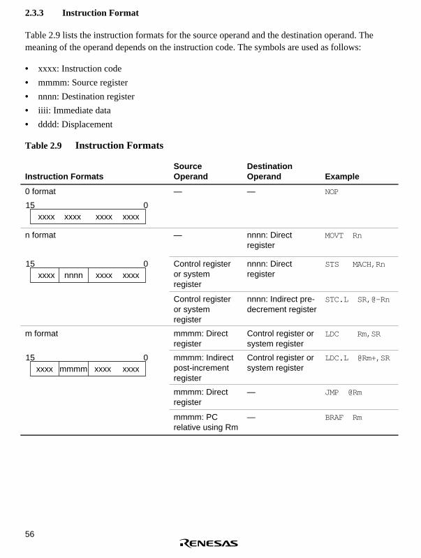
56
2.3.3 Instruction Format
Table 2.9 lists the instruction formats for the source operand and the destination operand. Themeaning of the operand depends on the instruction code. The symbols are used as follows:
• xxxx: Instruction code
• mmmm: Source register
• nnnn: Destination register
• iiii: Immediate data
• dddd: Displacement
Table 2.9 Instruction Formats
Instruction FormatsSourceOperand
DestinationOperand Example
0 format
xxxx xxxx xxxxxxxx15 0
— — NOP
n format — nnnn: Directregister
MOVT Rn
xxxx xxxx xxxxnnnn15 0 Control register
or systemregister
nnnn: Directregister
STS MACH,Rn
Control registeror systemregister
nnnn: Indirect pre-decrement register
STC.L SR,@-Rn
m format mmmm: Directregister
Control register orsystem register
LDC Rm,SR
xxxxmmmmxxxx xxxx15 0 mmmm: Indirect
post-incrementregister
Control register orsystem register
LDC.L @Rm+,SR
mmmm: Directregister
— JMP @Rm
mmmm: PCrelative using Rm
— BRAF Rm

57
Table 2.9 Instruction Formats (cont)
Instruction FormatsSource Operand Destination
Operand Example
nm format mmmm: Directregister
nnnn: Directregister
ADD Rm,Rn
nnnnxxxx xxxx15 0
mmmmmmmm: Directregister
nnnn: Indirectregister
MOV.L Rm,@Rn
mmmm: Indirectpost-incrementregister (multiply/accumulate)
nnnn* : Indirectpost-incrementregister (multiply/accumulate)
MACH, MACL MAC.W@Rm+,@Rn+
mmmm: Indirectpost-incrementregister
nnnn: Directregister
MOV.L @Rm+,Rn
mmmm: Directregister
nnnn: Indirect pre-decrementregister
MOV.L Rm,@-Rn
mmmm: Directregister
nnnn: Indirectindexed register
MOV.LRm,@(R0,Rn)
md format
xxxx dddd15 0
mmmmxxxx
mmmmdddd:indirect registerwithdisplacement
R0 (Directregister)
MOV.B@(disp,Rm),R0
nd4 format
xxxxxxxx dddd15 0
nnnn
R0 (Directregister)
nnnndddd:Indirect registerwith displacement
MOV.BR0,@(disp,Rn)
nmd format
nnnnxxxx dddd15 0
mmmm
mmmm: Directregister
nnnndddd: Indirectregister withdisplacement
MOV.LRm,@(disp,Rn)
mmmmdddd:Indirect registerwithdisplacement
nnnn: Directregister
MOV.L@(disp,Rm),Rn
Note: * In multiply/accumulate instructions, nnnn is the source register.

58
Table 2.9 Instruction Formats (cont)
Instruction FormatsSource Operand Destination
Operand Example
d format
ddddxxxx15 0
xxxx dddd
dddddddd:Indirect GBRwithdisplacement
R0 (Direct register) MOV.L@(disp,GBR),R0
R0(Directregister)
dddddddd: IndirectGBR withdisplacement
MOV.LR0,@(disp,GBR)
dddddddd: PCrelative withdisplacement
R0 (Direct register) MOVA@(disp,PC),R0
dddddddd: PCrelative
— BF label
d12 format
ddddxxxx15 0
dddd dddd
dddddddddddd:PC relative
— BRA label
(label = disp +PC)
nd8 format
ddddnnnnxxxx15 0
dddd
dddddddd: PCrelative withdisplacement
nnnn: Directregister
MOV.L@(disp,PC),Rn
i format iiiiiiii: Immediate Indirect indexedGBR
AND.B#imm,@(R0,GBR)
xxxxxxxx i i i i15 0
i i i iiiiiiiii: Immediate R0 (Direct register) AND #imm,R0
iiiiiiii: Immediate — TRAPA #imm
ni format
nnnn i i i ixxxx15 0
i i i i
iiiiiiii: Immediate nnnn: Directregister
ADD #imm,Rn

59
2.4 Instruction Set by Classification
Table 2.10 Classification of Instructions
Classification TypesOperationCode Function
No. ofInstructions
Data transfer 5 MOV Data transfer, immediate data transfer,peripheral module data transfer, structure datatransfer
39
MOVA Effective address transfer
MOVT T bit transfer
SWAP Swap of upper and lower bytes
XTRCT Extraction of the middle of registers connected
Arithmetic 21 ADD Binary addition 33operations ADDC Binary addition with carry
ADDV Binary addition with overflow check
CMP/cond Comparison
DIV1 Division
DIV0S Initialization of signed division
DIV0U Initialization of unsigned division
DMULS Signed double-length multiplication
DMULU Unsigned double-length multiplication
DT Decrement and test
EXTS Sign extension
EXTU Zero extension
MAC Multiply/accumulate, double-lengthmultiply/accumulate operation
MUL Double-length multiply operation
MULS Signed multiplication
MULU Unsigned multiplication
NEG Negation
NEGC Negation with borrow
SUB Binary subtraction
SUBC Binary subtraction with borrow
SUBV Binary subtraction with underflow

60
Table 2.10 Classification of Instructions (cont)
Classification TypesOperationCode Function
No. ofInstructions
Logic 6 AND Logical AND 14operations NOT Bit inversion
OR Logical OR
TAS Memory test and bit set
TST Logical AND and T bit set
XOR Exclusive OR
Shift 10 ROTL One-bit left rotation 14
ROTR One-bit right rotation
ROTCL One-bit left rotation with T bit
ROTCR One-bit right rotation with T bit
SHAL One-bit arithmetic left shift
SHAR One-bit arithmetic right shift
SHLL One-bit logical left shift
SHLLn n-bit logical left shift
SHLR One-bit logical right shift
SHLRn n-bit logical right shift
Branch 9 BF Conditional branch, conditional branch withdelay (Branch when T = 0)
11
BT Conditional branch, conditional branch withdelay (Branch when T = 1)
BRA Unconditional branch
BRAF Unconditional branch
BSR Branch to subroutine procedure
BSRF Branch to subroutine procedure
JMP Unconditional branch
JSR Branch to subroutine procedure
RTS Return from subroutine procedure

61
Table 2.10 Classification of Instructions (cont)
Classification TypesOperationCode Function
No. ofInstructions
System 11 CLRT T bit clear 31control CLRMAC MAC register clear
LDC Load to control register
LDS Load to system register
NOP No operation
RTE Return from exception processing
SETT T bit set
SLEEP Shift into power-down mode
STC Storing control register data
STS Storing system register data
TRAPA Trap exception handling
Total: 62 142
Table 2.11 shows the format used in tables 2.12 to 2.17, which list instruction codes, operation,and execution states in order by classification.

62
Table 2.11 Instruction Code Format
Item Format Explanation
Instruction OP.Sz SRC,DEST OP: Operation codeSz: Size (B: byte, W: word, or L: longword)SRC: SourceDEST: DestinationRm: Source registerRn: Destination registerimm: Immediate datadisp: Displacement* 1
Instructioncode
MSB ↔ LSB mmmm: Source registernnnn: Destination register
0000: R00001: R1
. . .
1111: R15iiii: Immediate datadddd: Displacement
Operation →, ← Direction of transfer
(xx) Memory operand
M/Q/T Flag bits in the SR
& Logical AND of each bit
| Logical OR of each bit
^ Exclusive OR of each bit
~ Logical NOT of each bit
<<n n-bit left shift
>>n n-bit right shift
Executioncycles
— Value when no wait states are inserted* 2
T bit — Value of T bit after instruction is executed. An em-dash (—)in the column means no change.
Notes: * 1 Depending on the operand size, displacement is scaled ×1, ×2, or ×4. For details, seethe SH-1/SH-2/SH-DSP Programming Manual.
* 2 Instruction execution cycles: The execution cycles shown in the table are minimums.The actual number of cycles may be increased when (1) contention occurs betweeninstruction fetches and data access, or (2) when the destination register of the loadinstruction (memory → register) and the register used by the next instruction are thesame.

63
Table 2.12 Data Transfer Instructions
Instruction Instruction Code Operation
Execu-tionCycles
TBit
MOV #imm,Rn 1110nnnniiiiiiii #imm → Sign extension →Rn
1 —
MOV.W @(disp,PC),Rn 1001nnnndddddddd (disp × 2 + PC) → Signextension → Rn
1 —
MOV.L @(disp,PC),Rn 1101nnnndddddddd (disp × 4 + PC) → Rn 1 —
MOV Rm,Rn 0110nnnnmmmm0011 Rm → Rn 1 —
MOV.B Rm,@Rn 0010nnnnmmmm0000 Rm → (Rn) 1 —
MOV.W Rm,@Rn 0010nnnnmmmm0001 Rm → (Rn) 1 —
MOV.L Rm,@Rn 0010nnnnmmmm0010 Rm → (Rn) 1 —
MOV.B @Rm,Rn 0110nnnnmmmm0000 (Rm) → Sign extension →Rn
1 —
MOV.W @Rm,Rn 0110nnnnmmmm0001 (Rm) → Sign extension →Rn
1 —
MOV.L @Rm,Rn 0110nnnnmmmm0010 (Rm) → Rn 1 —
MOV.B Rm,@–Rn 0010nnnnmmmm0100 Rn–1 → Rn, Rm → (Rn) 1 —
MOV.W Rm,@–Rn 0010nnnnmmmm0101 Rn–2 → Rn, Rm → (Rn) 1 —
MOV.L Rm,@–Rn 0010nnnnmmmm0110 Rn–4 → Rn, Rm → (Rn) 1 —
MOV.B @Rm+,Rn 0110nnnnmmmm0100 (Rm) → Sign extension →Rn,Rm + 1 → Rm
1 —
MOV.W @Rm+,Rn 0110nnnnmmmm0101 (Rm) → Sign extension →Rn,Rm + 2 → Rm
1 —
MOV.L @Rm+,Rn 0110nnnnmmmm0110 (Rm) → Rn,Rm + 4 → Rm 1 —
MOV.B R0,@(disp,Rn) 10000000nnnndddd R0 → (disp + Rn) 1 —
MOV.W R0,@(disp,Rn) 10000001nnnndddd R0 → (disp × 2 + Rn) 1 —
MOV.L Rm,@(disp,Rn) 0001nnnnmmmmdddd Rm → (disp × 4 + Rn) 1 —
MOV.B @(disp,Rm),R0 10000100mmmmdddd (disp + Rm) → Signextension → R0
1 —
MOV.W @(disp,Rm),R0 10000101mmmmdddd (disp × 2 + Rm) → Signextension → R0
1 —
MOV.L @(disp,Rm),Rn 0101nnnnmmmmdddd (disp × 4 + Rm) → Rn 1 —
MOV.B Rm,@(R0,Rn) 0000nnnnmmmm0100 Rm → (R0 + Rn) 1 —
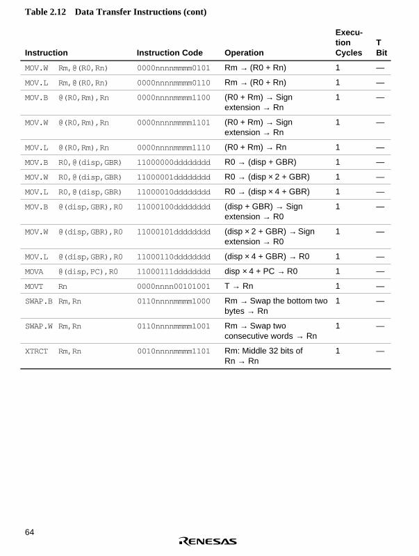
64
Table 2.12 Data Transfer Instructions (cont)
Instruction Instruction Code Operation
Execu-tionCycles
TBit
MOV.W Rm,@(R0,Rn) 0000nnnnmmmm0101 Rm → (R0 + Rn) 1 —
MOV.L Rm,@(R0,Rn) 0000nnnnmmmm0110 Rm → (R0 + Rn) 1 —
MOV.B @(R0,Rm),Rn 0000nnnnmmmm1100 (R0 + Rm) → Signextension → Rn
1 —
MOV.W @(R0,Rm),Rn 0000nnnnmmmm1101 (R0 + Rm) → Signextension → Rn
1 —
MOV.L @(R0,Rm),Rn 0000nnnnmmmm1110 (R0 + Rm) → Rn 1 —
MOV.B R0,@(disp,GBR) 11000000dddddddd R0 → (disp + GBR) 1 —
MOV.W R0,@(disp,GBR) 11000001dddddddd R0 → (disp × 2 + GBR) 1 —
MOV.L R0,@(disp,GBR) 11000010dddddddd R0 → (disp × 4 + GBR) 1 —
MOV.B @(disp,GBR),R0 11000100dddddddd (disp + GBR) → Signextension → R0
1 —
MOV.W @(disp,GBR),R0 11000101dddddddd (disp × 2 + GBR) → Signextension → R0
1 —
MOV.L @(disp,GBR),R0 11000110dddddddd (disp × 4 + GBR) → R0 1 —
MOVA @(disp,PC),R0 11000111dddddddd disp × 4 + PC → R0 1 —
MOVT Rn 0000nnnn00101001 T → Rn 1 —
SWAP.B Rm,Rn 0110nnnnmmmm1000 Rm → Swap the bottom twobytes → Rn
1 —
SWAP.W Rm,Rn 0110nnnnmmmm1001 Rm → Swap twoconsecutive words → Rn
1 —
XTRCT Rm,Rn 0010nnnnmmmm1101 Rm: Middle 32 bits ofRn → Rn
1 —

65
Table 2.13 Arithmetic Operation Instructions
Instruction Instruction Code Operation
Execu-tionCycles T Bit
ADD Rm,Rn 0011nnnnmmmm1100 Rn + Rm → Rn 1 —
ADD #imm,Rn 0111nnnniiiiiiii Rn + imm → Rn 1 —
ADDC Rm,Rn 0011nnnnmmmm1110 Rn + Rm + T → Rn,Carry → T
1 Carry
ADDV Rm,Rn 0011nnnnmmmm1111 Rn + Rm → Rn,Overflow → T
1 Overflow
CMP/EQ #imm,R0 10001000iiiiiiii If R0 = imm, 1 → T 1 Comparisonresult
CMP/EQ Rm,Rn 0011nnnnmmmm0000 If Rn = Rm, 1 → T 1 Comparisonresult
CMP/HS Rm,Rn 0011nnnnmmmm0010 If Rn≥Rm with unsigneddata, 1 → T
1 Comparisonresult
CMP/GE Rm,Rn 0011nnnnmmmm0011 If Rn ≥ Rm with signeddata, 1 → T
1 Comparisonresult
CMP/HI Rm,Rn 0011nnnnmmmm0110 If Rn > Rm withunsigned data, 1 → T
1 Comparisonresult
CMP/GT Rm,Rn 0011nnnnmmmm0111 If Rn > Rm with signeddata, 1 → T
1 Comparisonresult
CMP/PL Rn 0100nnnn00010101 If Rn > 0, 1 → T 1 Comparisonresult
CMP/PZ Rn 0100nnnn00010001 If Rn ≥ 0, 1 → T 1 Comparisonresult
CMP/STR Rm,Rn 0010nnnnmmmm1100 If Rn and Rm havean equivalent byte,1 → T
1 Comparisonresult
DIV1 Rm,Rn 0011nnnnmmmm0100 Single-step division(Rn/Rm)
1 Calculationresult
DIV0S Rm,Rn 0010nnnnmmmm0111 MSB of Rn → Q, MSBof Rm → M, M ^ Q → T
1 Calculationresult
DIV0U 0000000000011001 0 → M/Q/T 1 0

66
Table 2.13 Arithmetic Operation Instructions (cont)
Instruction Instruction Code Operation
Execu-tionCycles T Bit
DMULS.L Rm,Rn 0011nnnnmmmm1101 Signed operation of Rn× Rm → MACH, MACL32 × 32 → 64 bit
2 to 4* —
DMULU.L Rm,Rn 0011nnnnmmmm0101 Unsigned operation ofRn × Rm → MACH,MACL 32 × 32 → 64 bit
2 to 4* —
DT Rn 0100nnnn00010000 Rn – 1 → Rn, when Rnis 0, 1 → T. When Rn isnonzero, 0 → T
1 Comparisonresult
EXTS.B Rm,Rn 0110nnnnmmmm1110 A byte in Rm is sign-extended → Rn
1 —
EXTS.W Rm,Rn 0110nnnnmmmm1111 A word in Rm is sign-extended → Rn
1 —
EXTU.B Rm,Rn 0110nnnnmmmm1100 A byte in Rm is zero-extended → Rn
1 —
EXTU.W Rm,Rn 0110nnnnmmmm1101 A word in Rm is zero-extended → Rn
1 —
MAC.L @Rm+,@Rn+ 0000nnnnmmmm1111 Signed operation of(Rn) × (Rm) + MAC →MAC 32 × 32 → 64 bit
3/(2 to4)*
—
MAC.W @Rm+,@Rn+ 0100nnnnmmmm1111 Signed operation of(Rn) × (Rm) + MAC →MAC 16 × 16 + 64 →64 bit
3/(2)* —
MUL.L Rm,Rn 0000nnnnmmmm0111 Rn × Rm → MACL, 32× 32 → 32 bit
2 to 4* —
MULS.W Rm,Rn 0010nnnnmmmm1111 Signed operation of Rn× Rm → MAC 16 × 16→ 32 bit
1 to 3* —
MULU.W Rm,Rn 0010nnnnmmmm1110 Unsigned operation ofRn × Rm → MAC 16 ×16 → 32 bit
1 to 3* —
NEG Rm,Rn 0110nnnnmmmm1011 0–Rm → Rn 1 —
NEGC Rm,Rn 0110nnnnmmmm1010 0–Rm–T → Rn, Borrow→ T
1 Borrow

67
Table 2.13 Arithmetic Operation Instructions (cont)
Instruction Instruction Code Operation
Execu-tionCycles T Bit
SUB Rm,Rn 0011nnnnmmmm1000 Rn–Rm → Rn 1 —
SUBC Rm,Rn 0011nnnnmmmm1010 Rn–Rm–T → Rn,Borrow → T
1 Borrow
SUBV Rm,Rn 0011nnnnmmmm1011 Rn–Rm → Rn,Underflow → T
1 Overflow
Note: * The normal minimum number of execution cycles. (The number in parentheses is thenumber of cycles when there is contention with following instructions.)

68
Table 2.14 Logic Operation Instructions
Instruction Instruction Code Operation
Execu-tionCycles T Bit
AND Rm,Rn 0010nnnnmmmm1001 Rn & Rm → Rn 1 —
AND #imm,R0 11001001iiiiiiii R0 & imm → R0 1 —
AND.B #imm,@(R0,GBR) 11001101iiiiiiii (R0 + GBR) & imm →(R0 + GBR)
3 —
NOT Rm,Rn 0110nnnnmmmm0111 ~Rm → Rn 1 —
OR Rm,Rn 0010nnnnmmmm1011 Rn | Rm → Rn 1 —
OR #imm,R0 11001011iiiiiiii R0 | imm → R0 1 —
OR.B #imm,@(R0,GBR) 11001111iiiiiiii (R0 + GBR) | imm →(R0 + GBR)
3 —
TAS.B @Rn 0100nnnn00011011 If (Rn) is 0, 1 → T; 1 →MSB of (Rn)*
4 Testresult
TST Rm,Rn 0010nnnnmmmm1000 Rn & Rm; if the result is0, 1 → T
1 Testresult
TST #imm,R0 11001000iiiiiiii R0 & imm; if the result is0, 1 → T
1 Testresult
TST.B #imm,@(R0,GBR) 11001100iiiiiiii (R0 + GBR) & imm; ifthe result is 0, 1 → T
3 Testresult
XOR Rm,Rn 0010nnnnmmmm1010 Rn ^ Rm → Rn 1 —
XOR #imm,R0 11001010iiiiiiii R0 ^ imm → R0 1 —
XOR.B #imm,@(R0,GBR) 11001110iiiiiiii (R0 + GBR) ^ imm →(R0 + GBR)
3 —
Note: * The on-chip DMAC/DTC bus cycles are not inserted between the read and write cycles ofTAS instruction execution. However, bus release due to BREQ is carried out.

69
Table 2.15 Shift Instructions
Instruction Instruction Code Operation
Execu-tionCycles T Bit
ROTL Rn 0100nnnn00000100 T ← Rn ← MSB 1 MSB
ROTR Rn 0100nnnn00000101 LSB → Rn → T 1 LSB
ROTCL Rn 0100nnnn00100100 T ← Rn ← T 1 MSB
ROTCR Rn 0100nnnn00100101 T → Rn → T 1 LSB
SHAL Rn 0100nnnn00100000 T ← Rn ← 0 1 MSB
SHAR Rn 0100nnnn00100001 MSB → Rn → T 1 LSB
SHLL Rn 0100nnnn00000000 T ← Rn ← 0 1 MSB
SHLR Rn 0100nnnn00000001 0 → Rn → T 1 LSB
SHLL2 Rn 0100nnnn00001000 Rn<<2 → Rn 1 —
SHLR2 Rn 0100nnnn00001001 Rn>>2 → Rn 1 —
SHLL8 Rn 0100nnnn00011000 Rn<<8 → Rn 1 —
SHLR8 Rn 0100nnnn00011001 Rn>>8 → Rn 1 —
SHLL16 Rn 0100nnnn00101000 Rn<<16 → Rn 1 —
SHLR16 Rn 0100nnnn00101001 Rn>>16 → Rn 1 —

70
Table 2.16 Branch Instructions
Instruction Instruction Code OperationExec.Cycles
TBit
BF label 10001011dddddddd If T = 0, disp × 2 + PC → PC; if T =1, nop
3/1* —
BF/S label 10001111dddddddd Delayed branch, if T = 0, disp × 2 +PC → PC; if T = 1, nop
2/1* —
BT label 10001001dddddddd If T = 1, disp × 2 + PC → PC; if T =0, nop
3/1* —
BT/S label 10001101dddddddd Delayed branch, if T = 1, disp × 2 +PC → PC; if T = 0, nop
2/1* —
BRA label 1010dddddddddddd Delayed branch, disp × 2 + PC →PC
2 —
BRAF Rm 0000mmmm00100011 Delayed branch, Rm + PC → PC 2 —
BSR label 1011dddddddddddd Delayed branch, PC → PR, disp × 2+ PC → PC
2 —
BSRF Rm 0000mmmm00000011 Delayed branch, PC → PR,Rm + PC → PC
2 —
JMP @Rm 0100mmmm00101011 Delayed branch, Rm → PC 2 —
JSR @Rm 0100mmmm00001011 Delayed branch, PC → PR,Rm → PC
2 —
RTS 0000000000001011 Delayed branch, PR → PC 2 —
Note: * One state when it does not branch.
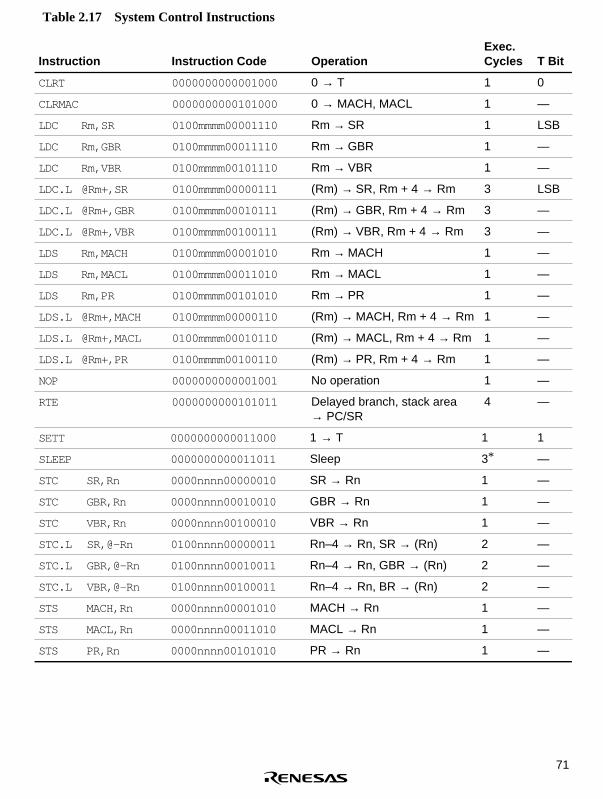
71
Table 2.17 System Control Instructions
Instruction Instruction Code OperationExec.Cycles T Bit
CLRT 0000000000001000 0 → T 1 0
CLRMAC 0000000000101000 0 → MACH, MACL 1 —
LDC Rm,SR 0100mmmm00001110 Rm → SR 1 LSB
LDC Rm,GBR 0100mmmm00011110 Rm → GBR 1 —
LDC Rm,VBR 0100mmmm00101110 Rm → VBR 1 —
LDC.L @Rm+,SR 0100mmmm00000111 (Rm) → SR, Rm + 4 → Rm 3 LSB
LDC.L @Rm+,GBR 0100mmmm00010111 (Rm) → GBR, Rm + 4 → Rm 3 —
LDC.L @Rm+,VBR 0100mmmm00100111 (Rm) → VBR, Rm + 4 → Rm 3 —
LDS Rm,MACH 0100mmmm00001010 Rm → MACH 1 —
LDS Rm,MACL 0100mmmm00011010 Rm → MACL 1 —
LDS Rm,PR 0100mmmm00101010 Rm → PR 1 —
LDS.L @Rm+,MACH 0100mmmm00000110 (Rm) → MACH, Rm + 4 → Rm 1 —
LDS.L @Rm+,MACL 0100mmmm00010110 (Rm) → MACL, Rm + 4 → Rm 1 —
LDS.L @Rm+,PR 0100mmmm00100110 (Rm) → PR, Rm + 4 → Rm 1 —
NOP 0000000000001001 No operation 1 —
RTE 0000000000101011 Delayed branch, stack area→ PC/SR
4 —
SETT 0000000000011000 1 → T 1 1
SLEEP 0000000000011011 Sleep 3* —
STC SR,Rn 0000nnnn00000010 SR → Rn 1 —
STC GBR,Rn 0000nnnn00010010 GBR → Rn 1 —
STC VBR,Rn 0000nnnn00100010 VBR → Rn 1 —
STC.L SR,@–Rn 0100nnnn00000011 Rn–4 → Rn, SR → (Rn) 2 —
STC.L GBR,@–Rn 0100nnnn00010011 Rn–4 → Rn, GBR → (Rn) 2 —
STC.L VBR,@–Rn 0100nnnn00100011 Rn–4 → Rn, BR → (Rn) 2 —
STS MACH,Rn 0000nnnn00001010 MACH → Rn 1 —
STS MACL,Rn 0000nnnn00011010 MACL → Rn 1 —
STS PR,Rn 0000nnnn00101010 PR → Rn 1 —

72
Table 2.17 System Control Instructions (cont)
Instruction Instruction Code OperationExec.Cycles T Bit
STS.L MACH,@–Rn 0100nnnn00000010 Rn–4 → Rn, MACH → (Rn) 1 —
STS.L MACL,@–Rn 0100nnnn00010010 Rn–4 → Rn, MACL → (Rn) 1 —
STS.L PR,@–Rn 0100nnnn00100010 Rn–4 → Rn, PR → (Rn) 1 —
TRAPA #imm 11000011iiiiiiii PC/SR → stack area,
(imm × 4 + VBR) → PC
8 —
Note: * The number of execution cycles before the chip enters sleep mode: The execution cyclesshown in the table are minimums. The actual number of cycles may be increased when(1) contention occurs between instruction fetches and data access, or (2) when thedestination register of the load instruction (memory → register) and the register used bythe next instruction are the same.
2.5 Processing States
2.5.1 State Transitions
The CPU has five processing states: reset, exception processing, bus release, program executionand power-down. Figure 2.6 shows the transitions between the states.

73
RES = 0
Power-on reset state Manual reset state
Sleep mode Standby mode
Program execution state
Bus release state
Exception processing state
RES = 1MRES = 1
RES = 1When an interrupt source
or DMA address error occurs
NMI interruptsource occurs
Exception processingends
Bus requestgenerated
Exceptionprocessing
source occurs
Bus requestcleared
Bus requestgenerated
Bus requestcleared
SBY bitcleared
for SLEEPinstruction
SBY bit set for SLEEP instruction
From any statewhen RES = 0
From any state whenRES = 1 and MRES = 0
Reset states
Power-down state
Bus requestgenerated
Bus requestcleared
Figure 2.6 Transitions between Processing States
Reset State: The CPU resets in the reset state. When the RES pin level goes low, a power-on resetresults. When the RES pin is high and MRES is low, a manual reset will occur.
Exception Processing State: The exception processing state is a transient state that occurs whenexception processing sources such as resets or interrupts alter the CPU’s processing state flow.

74
For a reset, the initial values of the program counter (PC) (execution start address) and stackpointer (SP) are fetched from the exception processing vector table and stored; the CPU thenbranches to the execution start address and execution of the program begins.
For an interrupt, the stack pointer (SP) is accessed and the program counter (PC) and statusregister (SR) are saved to the stack area. The exception service routine start address is fetchedfrom the exception processing vector table; the CPU then branches to that address and the programstarts executing, thereby entering the program execution state.
Program Execution State: In the program execution state, the CPU sequentially executes theprogram.
Power-Down State: In the power-down state, the CPU operation halts and power consumptiondeclines. The SLEEP instruction places the CPU in the power-down state. This state has twomodes: sleep mode and standby mode.
Bus Release State: In the bus release state, the CPU releases access rights to the bus to the devicethat has requested them.
2.5.2 Power-Down State
Besides the ordinary program execution states, the CPU also has a power-down state in whichCPU operation halts, lowering power consumption. There are two power-down state modes: sleepmode and standby mode.
Sleep Mode: When standby bit SBY (in the standby control register SBYCR) is cleared to 0 and aSLEEP instruction executed, the CPU moves from program execution state to sleep mode. In thesleep mode, the CPU halts and the contents of its internal registers and the data in on-chip cache(or on-chip RAM) is maintained. The on-chip peripheral modules other than the CPU do not haltin the sleep mode.
To return from sleep mode, use a reset (power-on or manual), any interrupt, or a DMA addresserror; the CPU returns to the ordinary program execution state through the exception processingstate.
Standby Mode: To enter the standby mode, set the standby bit SBY (in the standby controlregister SBYCR) to 1 and execute a SLEEP instruction. In standby mode, all CPU, on-chipperipheral module, and oscillator functions are halted. However, when entering standby mode, theDMA master enable bit of the DMAC should be set to 0. If multiplication-related instructions arebeing executed at the time of entry into standby mode, the values of MACH and MACL willbecome undefined.
To return from standby mode, use a reset (power-on or manual) or an NMI interrupt. For resets,the CPU returns to ordinary program execution state through the exception processing state whenplaced in a reset state for the duration of the oscillator stabilization time. For NMI interrupts, the

75
CPU returns to ordinary program execution state through the exception processing state after theoscillator stabilization time has elapsed. In this mode, power consumption drops markedly, sincethe oscillator stops (table 2.18).
Table 2.18 Power-Down State
State
ModeTransitionConditions Clock CPU
On-ChipPeripheralModules
CPURegisters
On-ChipCache orOn-ChipRAM
I/OPortPins Canceling
Sleep ExecuteSLEEPinstructionwith SBY bitcleared to 0in SBYCR
Run Halt Run Held Held Held • Interrupt
• DMA addresserror
• Power-on reset
• Manual reset
Stand-by
ExecuteSLEEPinstructionwith SBY bitset to 1 inSBYCR
Halt Halt Halt andinitialize*
Held Held Held orHi-Z(select-able)
• NMI interrupt
• Power-on reset
• Manual reset
Note: * Differs depending on the peripheral module and pin.

76

77
Section 3 Operating Modes
3.1 Operating Modes, Types, and Selection
This LSI has five operating modes and three clock modes, determined by the setting of the modepins (MD3–MD0). Do not change the mode pin settings during LSI operation (while power is on).(In the F-ZTAT version, however, MD1 can be changed in the power-on reset state.)
Table 3.1 indicates the setting method for the operating mode.
Table 3.1 Operating Mode Setting
Mode Pin Setting Mode On-Chip CS0 Area
No. FWP MD3* 1 MD2* 1 MD1 MD0 Name ROM 112 Pin 144 Pin
0 1 x x 0 0 MCU mode 0 Not Active 8-bit space 16-bitspace
1 1 x x 0 1 MCU mode 1 Not Active 16-bit space 32-bitspace
2 1 x x 1 0 MCU mode 2 Active 8/16-bitspace* 2
8/16/32-bitspace* 2
3 1 x x 1 1 Single chipmode
Active — —
4 1 1 1 1 1 PROM mode* 3 Active — —
— 0 x x 0 0 Boot mode* 4 Active 8/16-bitspace* 2
8/16/32-bitspace* 2
— 0 x x 0 1 — —
— 0 x x 1 0 Userprogrammingmode* 4
Active 8/16-bitspace* 2
8/16/32-bitspace* 2
— 0 x x 1 1 — —
— 1 1 1 0 1 Flashprogrammermode* 4
Active — —
Notes: * 1 MD2 and MD3 pins select the clock mode in modes 0–3 (table 3.2).* 2 Set by BCR2 of BSC.* 3 Only ZTAT.* 4 Only F-ZTAT.
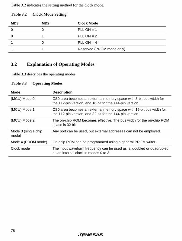
78
Table 3.2 indicates the setting method for the clock mode.
Table 3.2 Clock Mode Setting
MD3 MD2 Clock Mode
0 0 PLL ON × 1
0 1 PLL ON × 2
1 0 PLL ON × 4
1 1 Reserved (PROM mode only)
3.2 Explanation of Operating Modes
Table 3.3 describes the operating modes.
Table 3.3 Operating Modes
Mode Description
(MCU) Mode 0 CS0 area becomes an external memory space with 8-bit bus width forthe 112-pin version, and 16-bit for the 144-pin version.
(MCU) Mode 1 CS0 area becomes an external memory space with 16-bit bus width forthe 112-pin version, and 32-bit for the 144-pin version
(MCU) Mode 2 The on-chip ROM becomes effective. The bus width for the on-chip ROMspace is 32 bit.
Mode 3 (single chipmode)
Any port can be used, but external addresses can not be employed.
Mode 4 (PROM mode) On-chip ROM can be programmed using a general PROM writer.
Clock mode The input waveform frequency can be used as is, doubled or quadrupledas an internal clock in modes 0 to 3.

79
3.3 Pin Configuration
Table 3.4 describes the function of each operating mode related pin.
Table 3.4 Operating Mode Pin Function
PinName Input/Output Function
XTAL Input Connects to a crystal oscillator
EXTAL Input Connects to a crystal oscillator, or used for external clock input pin
PLLCAP Input Connects to a capacitor for PLL circuit operation
MD0 Input Designates operating mode through the level applied to this pin
MD1 Input Designates operating mode through the level applied to this pin
MD2 Input Designates clock mode through the level applied to this pin
MD3 Input Designates clock mode through the level applied to this pin

80

81
Section 4 Clock Pulse Generator (CPG)
4.1 Overview
The SH7040 Series has an on-chip clock pulse generator (CPG) that generates the system clock(φ), as well as the internal clock (φ/2 to φ/8192). The CPG consists of an oscillator, a PLL, and aprescaler.
4.1.1 Block Diagram
A block diagram of the clock pulse generator is shown in figure 4.1.
PLLCAP
CK
EXTAL
XTAL
MD2
MD3
Oscillator PLL circuit
Clock modecontrol circuitry
Prescaler
Within the LSI
φ φ/2 toφ/8192
Figure 4.1 Block Diagram of the Clock Pulse Generator
4.2 Oscillator
Clock pulses can be supplied from a connected crystal resonator or an external clock.
4.2.1 Connecting a Crystal Oscillator
Circuit Configuration: A crystal oscillator can be connected as shown in figure 4.2. Use thedamping resistance (Rd) listed in table 4.1. Use a 4–10 MHz crystal oscillator (consult your dealerconcerning the compatibility of the crystal oscillator and the LSI).

82
XTAL
EXTAL
CL1
CL2
Rd
4–10 MHz
CL1 = CL2 = 18–22 pF (Recommended value)
Figure 4.2 Connection of the Crystal Oscillator (Example)
Table 4.1 Damping Resistance Values (Recommended Values)
Frequency (MHz)
Parameter 4 8 10
Rd (Ω) 500 200 0
Crystal Oscillator: Figure 4.3 shows an equivalent circuit of the crystal oscillator. Use a crystaloscillator with the characteristics listed in table 4.2.
CoEXTAL
CLL Rs
XTAL
Figure 4.3 Crystal Oscillator Equivalent Circuit
Table 4.2 Crystal Oscillator Parameters
Frequency (MHz)
Parameter 4 8 10
Rs max (Ω) 120 80 60
Co max (pF) 7 7 7
4.2.2 External Clock Input Method
Figure 4.4 shows an example of an external clock input connection. In this case, make the externalclock high level to stop it when in standby mode. During operation, make the external input clockfrequency 4–10 MHz.
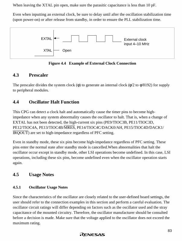
83
When leaving the XTAL pin open, make sure the parasitic capacitance is less than 10 pF.
Even when inputting an external clock, be sure to delay until after the oscillation stabilization time(upon power-on) or after release from standby, in order to ensure the PLL stabilization time.
EXTAL
XTAL Open
External clockinput 4–10 MHz
Figure 4.4 Example of External Clock Connection
4.3 Prescaler
The prescaler divides the system clock (φ) to generate an internal clock (φ/2 to φ/8192) for supplyto peripheral modules.
4.4 Oscillator Halt Function
This CPG can detect a clock halt and automatically cause the timer pins to become high-impedance when any system abnormality causes the oscillator to halt. That is, when a change ofEXTAL has not been detected, the high-current six pins (PE9/TIOC3B, PE11/TIOC3D,PE12/TIOC4A, PE13/TIOC4B/MRES, PE14/TIOC4C/DACK0/AH, PE15/TIOC4D/DACK1/IRQOUT) are set to high-impedance regardless of PFC setting.
Even in standby mode, these six pins become high-impedance regardless of PFC setting. Thesepins enter the normal state after standby mode is cancelled.When abnormalities that halt theoscillator occur except in standby mode, other LSI operations become undefined. In this case, LSIoperations, including these six pins, become undefined even when the oscillator operation startsagain.
4.5 Usage Notes
4.5.1 Oscillator Usage Notes
Since the characteristics of the oscillator are closely related to the user-defined board settings, theuser should refer to the connection examples in this section and perform a careful evaluation. Theoscillator circuit ratings will differ depending on factors such as the oscillator used and the straycapacitance of the mounted circuitry. Therefore, the oscillator manufacturer should be consultedbefore a decision is made. Make sure that the voltage applied to the oscillator does not exceed themaximum rating.

84
4.5.2 Notes on Board Design
When connecting a crystal oscillator, observe the following precautions:
• To prevent induction from interfering with correct oscillation, do not route any signal linesnear the oscillator circuitry.
• When designing the board, place the crystal oscillator and its load capacitors as close aspossible to the XTAL and EXTAL pins.
Figure 4.5 shows the precautions regarding oscillator block board settings.
Crossing of signallines prohibited
CL1XTAL
EXTALCL2
Figure 4.5 Cautions for Oscillator Circuit System Board Design

85
External circuitry such as that shown in figure 4.6 is recommended around the PLL.
PLLCAP
PLLVCC
PLLVSS
VCC
VSS
R1: 3 kΩ C1: 470 pF
Rp: 200 Ω
CPB: 0.1 µF*
CB: 0.1 µF*
Note: * CB and CPB are laminated ceramic capacitors
(Recommended values)
Figure 4.6 Cautions for Use of PLL Oscillator Circuit
Place oscillation stabilization capacitor C1 and resistor R1 near the PLLCAP pin, and ensure thatthese lines do not cross any other signal lines. Supply the C1 ground from PLLVSS.
Also, separate PLLVCC and PLLVSS, and the other VCC and VSS pins, from the board power supplysource, and be sure to insert bypass capacitors CPB and CB close to the pins.
If V CC and PLLVCC are both 3.3 V ± 0.3 V, it is recommended that Rp be set to 0 Ω.
4.5.3 Spread Spectrum Clock Generator Usage Notes
The following points should be borne in mind when using a spread spectrum clock generator as anexternal oscillator in order to reduce radiation noise.
• Set the center frequency and the spread amplitude such that the internal clock does not exceedthe maximum frequency during spread spectrum operation.
• Using a spread spectrum clock generator may trigger the oscillator halt function described insection 4.4. If the system configuration is such that this function will cause problems, a spreadspectrum clock generator should not be used.

86

87
Section 5 Exception Processing
5.1 Overview
5.1.1 Types of Exception Processing and Priority
Exception processing is started by four sources: resets, address errors, interrupts and instructionsand have the priority shown in table 5.1. When several exception processing sources occur at once,they are processed according to the priority shown.
Table 5.1 Types of Exception Processing and Priority Order
Exception Source Priority
Reset Power-on reset High
Manual reset
Address CPU address errorerror DMAC/DTC address error
Interrupt NMI
User break
IRQ
On-chip peripheral modules: • Direct memory access controller (DMAC)
• Multifunction timer/pulse unit (MTU)
• Serial communications interface (SCI)
• A/D converter (A/D)* 3
• Data transfer controller (DTC)
• Compare match timer (CMT)
• Watchdog timer (WDT)
• Bus state controller (BSC)
• Port output enable control section
Instructions Trap instruction (TRAPA instruction)
General illegal instructions (undefined code)
Illegal slot instructions (undefined code placed directly after a delay branchinstruction* 1 or instructions that rewrite the PC* 2)
Low
Notes: * 1 Delayed branch instructions: JMP, JSR, BRA, BSR, RTS, RTE, BF/S, BT/S, BSRF,BRAF.
* 2 Instructions that rewrite the PC: JMP, JSR, BRA, BSR, RTS, RTE, BT, BF, TRAPA,BF/S, BT/S, BSRF, BRAF.
* 3 A mask products: A/D0, A/D1.

88
5.1.2 Exception Processing Operations
The exception processing sources are detected and begin processing according to the timingshown in table 5.2.
Table 5.2 Timing of Exception Source Detection and the Start of Exception Processing
Exception Source Timing of Source Detection and Start of Processing
Reset Power-on reset Starts when the RES pin changes from low to high.
Manual reset Starts when the RES pin is high and the MRES pin changesfrom low to high.
Address error Detected when instruction is decoded and starts when theprevious executing instruction finishes executing.
Interrupts Detected when instruction is decoded and starts when theprevious executing instruction finishes executing.
Instructions Trap instruction Starts from the execution of a TRAPA instruction.
General illegalinstructions
Starts from the decoding of undefined code anytime except aftera delayed branch instruction (delay slot).
Illegal slotinstructions
Starts from the decoding of undefined code placed in a delayedbranch instruction (delay slot) or of instructions that rewrite thePC.
When exception processing starts, the CPU operates as follows:
1. Exception processing triggered by reset:
The initial values of the program counter (PC) and stack pointer (SP) are fetched from theexception processing vector table (PC and SP are respectively the H'00000000 andH'00000004 addresses for power-on resets and the H'00000008 and H'0000000C addresses formanual resets). See section 5.1.3, Exception Processing Vector Table, for more information. 0is then written to the vector base register (VBR) and 1111 is written to the interrupt mask bits(I3–I0) of the status register (SR). The program begins running from the PC address fetchedfrom the exception processing vector table.
2. Exception processing triggered by address errors, interrupts and instructions:
SR and PC are saved to the stack indicated by R15. For interrupt exception processing, theinterrupt priority level is written to the SR’s interrupt mask bits (I3–I0). For address error andinstruction exception processing, the I3–I0 bits are not affected. The start address is thenfetched from the exception processing vector table and the program begins running from thataddress.
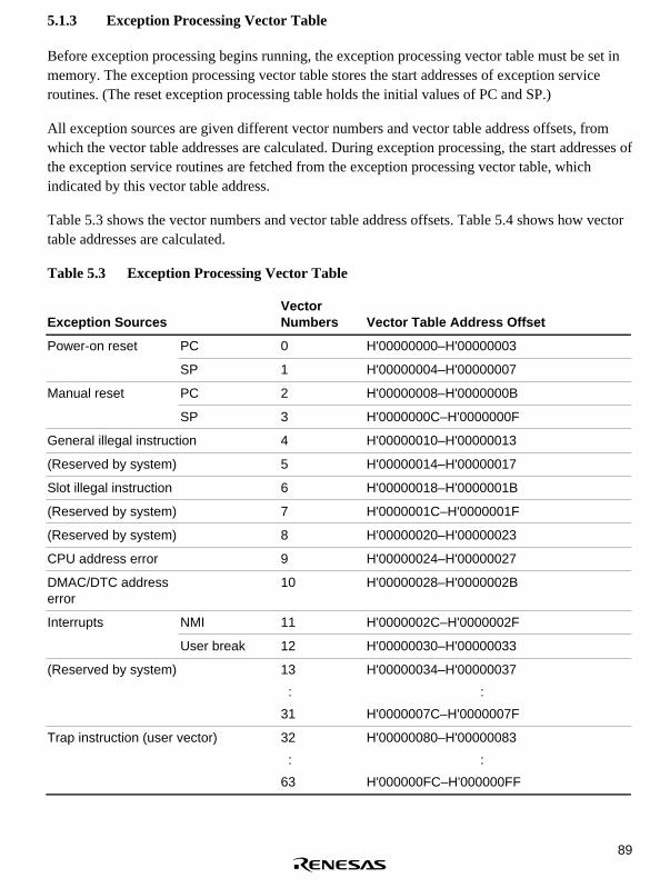
89
5.1.3 Exception Processing Vector Table
Before exception processing begins running, the exception processing vector table must be set inmemory. The exception processing vector table stores the start addresses of exception serviceroutines. (The reset exception processing table holds the initial values of PC and SP.)
All exception sources are given different vector numbers and vector table address offsets, fromwhich the vector table addresses are calculated. During exception processing, the start addresses ofthe exception service routines are fetched from the exception processing vector table, whichindicated by this vector table address.
Table 5.3 shows the vector numbers and vector table address offsets. Table 5.4 shows how vectortable addresses are calculated.
Table 5.3 Exception Processing Vector Table
Exception SourcesVectorNumbers Vector Table Address Offset
Power-on reset PC 0 H'00000000–H'00000003
SP 1 H'00000004–H'00000007
Manual reset PC 2 H'00000008–H'0000000B
SP 3 H'0000000C–H'0000000F
General illegal instruction 4 H'00000010–H'00000013
(Reserved by system) 5 H'00000014–H'00000017
Slot illegal instruction 6 H'00000018–H'0000001B
(Reserved by system) 7 H'0000001C–H'0000001F
(Reserved by system) 8 H'00000020–H'00000023
CPU address error 9 H'00000024–H'00000027
DMAC/DTC addresserror
10 H'00000028–H'0000002B
Interrupts NMI 11 H'0000002C–H'0000002F
User break 12 H'00000030–H'00000033
(Reserved by system) 13
:
31
H'00000034–H'00000037
:
H'0000007C–H'0000007F
Trap instruction (user vector) 32
:
63
H'00000080–H'00000083
:
H'000000FC–H'000000FF

90
Table 5.3 Exception Processing Vector Table (cont)
Exception SourcesVectorNumbers Vector Table Address Offset
Interrupts IRQ0 64 H'00000100–H'00000103
IRQ1 65 H'00000104–H'00000107
IRQ2 66 H'00000108–H'0000010B
IRQ3 67 H'0000010C–H'0000010F
IRQ4 68 H'00000110–H'00000113
IRQ5 69 H'00000114–H'00000117
IRQ6 70 H'00000118–H'0000011B
IRQ7 71 H'0000011C–H'0000011F
On-chip peripheralmodule*
72
:
255
H'00000120–H'00000124
:
H'000003FC–H'000003FF
Note: * The vector numbers and vector table address offsets for each on-chip peripheral moduleinterrupt are given in section 6, Interrupt Controller (INTC), and table 6.3, InterruptException Processing Vectors and Priorities.
Table 5.4 Calculating Exception Processing Vector Table Addresses
Exception Source Vector Table Address Calculation
Resets Vector table address = (vector table address offset)= (vector number) × 4
Address errors, interrupts,instructions
Vector table address = VBR + (vector table address offset)= VBR + (vector number) × 4
Notes: 1. VBR: Vector base register2. Vector table address offset: See table 5.3.3. Vector number: See table 5.3.
5.2 Resets
Resets have the highest priority of any exception source. There are two types of resets: manualresets and power-on resets. As table 5.5 shows, both types of resets initialize the internal status ofthe CPU. In power-on resets, all registers of the on-chip peripheral modules are initialized; inmanual resets, they are not.

91
Table 5.5 Types of Resets
Conditions for Transitionto Reset Status Internal Status
Type RES MRES CPU On-Chip Peripheral Module
Power-on reset Low — Initialized Initialized
Manual reset High Low Initialized Not initialized
5.2.1 Power-On Reset
When the RES pin is driven low, the LSI does a power-on reset. To reliably reset the LSI, the RESpin should be kept at low for at least the duration of the oscillation settling time when applyingpower or when in standby mode (when the clock circuit is halted) or at least 20 tcyc (when theclock circuit is running). During power-on reset, CPU internal status and all registers of on-chipperipheral modules are initialized. See Appendix C, Pin States, for the status of individual pinsduring the power-on reset status.
In the power-on reset status, power-on reset exception processing starts when the RES pin is firstdriven low for a set period of time and then returned to high. The CPU will then operate asfollows:
1. The initial value (execution start address) of the program counter (PC) is fetched from theexception processing vector table.
2. The initial value of the stack pointer (SP) is fetched from the exception processing vector table.
3. The vector base register (VBR) is cleared to H'00000000 and the interrupt mask bits (I3–I0) ofthe status register (SR) are set to H'F (1111).
4. The values fetched from the exception processing vector table are set in the program counter(PC) and SP and the program begins executing.
Be certain to always perform power-on reset processing when turning the system power on.
5.2.2 Manual Reset
When the RES pin is high and the MRES pin is driven low, the LSI does a manual reset. Toreliably reset the LSI, the MRES pin should be kept at low for at least the duration of theoscillation settling time when in standby mode (when the clock is halted) or at least 20 tcyc whenthe clock is operating. During manual reset, the CPU internal status is initialized. Registers of on-chip peripheral modules are not initialized. Since the BSC is not affected, the DRAM refreshcontrol functions remain operational even when the manual reset status continues for a long periodof time. When the LSI enters manual reset status in the middle of a bus cycle, manual resetexception processing does not start until the bus cycle has ended. Thus, manual resets do not abortbus cycles. However, the bus cycle ends once MRES is driven low. Hold at low level until manual

92
reset mode. (Keep at low level for at least the longest bus cycle.) See Appendix C, Pin States, forthe status of individual pins during manual reset mode.
In the manual reset status, manual reset exception processing starts when the MRES pin is firstkept low for a set period of time and then returned to high. The CPU will then operate the same asdescribed for power-on resets.
5.3 Address Errors
Address errors occur when instructions are fetched or data read or written, as shown in table 5.6.
Table 5.6 Bus Cycles and Address Errors
Bus Cycle
TypeBusMaster Bus Cycle Description Address Errors
Instruction CPU Instruction fetched from even address None (normal)
fetch Instruction fetched from odd address Address error occurs
Instruction fetched from other than on-chipperipheral module space*
None (normal)
Instruction fetched from on-chip peripheral modulespace*
Address error occurs
Instruction fetched from external memory spacewhen in single chip mode
Address error occurs
Data CPU or Word data accessed from even address None (normal)
read/write DMAC Word data accessed from odd address Address error occurs
or DTC Longword data accessed from a longwordboundary
None (normal)
Longword data accessed from other than a long-word boundary
Address error occurs
Byte or word data accessed in on-chip peripheralmodule space*
None (normal)
Longword data accessed in 16-bit on-chipperipheral module space*
None (normal)
Longword data accessed in 8-bit on-chip peripheralmodule space*
Address error occurs
External memory space accessed when in singlechip mode
Address error occurs
Note: * See section 10, Bus State Controller (BSC).

93
5.3.1 Address Error Exception Processing
When an address error occurs, the bus cycle in which the address error occurred ends. When theexecuting instruction then finishes, address error exception processing starts up. The CPU operatesas follows:
1. The status register (SR) is saved to the stack.
2. The program counter (PC) is saved to the stack. The PC value saved is the start address of theinstruction to be executed after the last executed instruction.
3. The exception service routine start address is fetched from the exception processing vectortable that corresponds to the address error that occurred and the program starts executing fromthat address. The jump that occurs is not a delayed branch.
5.4 Interrupts
Table 5.7 shows the sources that start up interrupt exception processing. These are divided intoNMI, user breaks, IRQ, and on-chip peripheral modules.
Table 5.7 Interrupt Sources
Type Request SourceNumber ofSources
NMI NMI pin (external input) 1
User break User break controller 1
IRQ IRQ0–IRQ7 (external input) 8
On-chip peripheral module Direct memory access controller (DMAC) 4
Multifunction timer/pulse unit (MTU) 24
Serial communications interface (SCI) 8
A/D converter 1*
Data transfer controller (DTC) 1
Compare match timer (CMT) 2
Watchdog timer (WDT) 1
Bus state controller (BSC) 1
Port 1
Note: * For A mask products, (A/D0, A/D1) is 2
Each interrupt source is allocated a different vector number and vector table offset. See section 6,Interrupt Controller (INTC), and table 6.3, Interrupt Exception Processing Vectors and Priorities,for more information on vector numbers and vector table address offsets.

94
5.4.1 Interrupt Priority Level
The interrupt priority order is predetermined. When multiple interrupts occur simultaneously(overlap), the interrupt controller (INTC) determines their relative priorities and starts upprocessing according to the results.
The priority order of interrupts is expressed as priority levels 0–16, with priority 0 the lowest andpriority 16 the highest. The NMI interrupt has priority 16 and cannot be masked, so it is alwaysaccepted. The user break interrupt priority level is 15. IRQ interrupts and on-chip peripheralmodule interrupt priority levels can be set freely using the INTC’s interrupt priority level settingregisters A through H (IPRA–IPRH) as shown in table 5.8. The priority levels that can be set are0–15. Level 16 cannot be set. See section 6.3.1, Interrupt Priority Registers A-H (IPRA-IPRH), formore information on IPRA to IPRH.
Table 5.8 Interrupt Priority Order
Type Priority Level Comment
NMI 16 Fixed priority level. Cannot be masked.
User break 15 Fixed priority level.
IRQ 0–15 Set with interrupt priority level setting registers Athrough H (IPRA–IPRH).
On-chip peripheral module 0–15 Set with interrupt priority level setting registers Athrough H (IPRA–IPRH).
5.4.2 Interrupt Exception Processing
When an interrupt occurs, its priority level is ascertained by the interrupt controller (INTC). NMIis always accepted, but other interrupts are only accepted if they have a priority level higher thanthe priority level set in the interrupt mask bits (I3–I0) of the status register (SR).
When an interrupt is accepted, exception processing begins. In interrupt exception processing, theCPU saves SR and the program counter (PC) to the stack. The priority level value of the acceptedinterrupt is written to SR bits I3–I0. For NMI, however, the priority level is 16, but the value set inI3–I0 is H'F (level 15). Next, the start address of the exception service routine is fetched from theexception processing vector table for the accepted interrupt, that address is jumped to andexecution begins. See section 6.4, Interrupt Operation, for more information on the interruptexception processing.
5.5 Exceptions Triggered by Instructions
Exception processing can be triggered by trap instructions, general illegal instructions, and illegalslot instructions, as shown in table 5.9.

95
Table 5.9 Types of Exceptions Triggered by Instructions
Type Source Instruction Comment
Trap instructions TRAPA —
Illegal slotinstructions
Undefined code placedimmediately after a delayedbranch instruction (delay slot)and instructions that rewrite thePC
Delayed branch instructions: JMP, JSR,BRA, BSR, RTS, RTE, BF/S, BT/S, BSRF,BRAF
Instructions that rewrite the PC: JMP, JSR,BRA, BSR, RTS, RTE, BT, BF, TRAPA,BF/S, BT/S, BSRF, BRAF
General illegalinstructions
Undefined code anywherebesides in a delay slot
—
5.5.1 Trap Instructions
When a TRAPA instruction is executed, trap instruction exception processing starts up. The CPUoperates as follows:
1. The status register (SR) is saved to the stack.
2. The program counter (PC) is saved to the stack. The PC value saved is the start address of theinstruction to be executed after the TRAPA instruction.
3. The exception service routine start address is fetched from the exception processing vectortable that corresponds to the vector number specified in the TRAPA instruction. That addressis jumped to and the program starts executing. The jump that occurs is not a delayed branch.
5.5.2 Illegal Slot Instructions
An instruction placed immediately after a delayed branch instruction is said to be placed in a delayslot. When the instruction placed in the delay slot is undefined code, illegal slot exceptionprocessing starts up when that undefined code is decoded. Illegal slot exception processing alsostarts up when an instruction that rewrites the program counter (PC) is placed in a delay slot. Theprocessing starts when the instruction is decoded. The CPU handles an illegal slot instruction asfollows:
1. The status register (SR) is saved to the stack.
2. The program counter (PC) is saved to the stack. The PC value saved is the jump address of thedelayed branch instruction immediately before the undefined code or the instruction thatrewrites the PC.
3. The exception service routine start address is fetched from the exception processing vectortable that corresponds to the exception that occurred. That address is jumped to and theprogram starts executing. The jump that occurs is not a delayed branch.

96
5.5.3 General Illegal Instructions
When undefined code placed anywhere other than immediately after a delayed branch instruction(i.e., in a delay slot) is decoded, general illegal instruction exception processing starts up. TheCPU handles general illegal instructions the same as illegal slot instructions. Unlike processing ofillegal slot instructions, however, the program counter value stored is the start address of theundefined code.
5.6 When Exception Sources Are Not Accepted
When an address error or interrupt is generated after a delayed branch instruction or interrupt-disabled instruction, it is sometimes not accepted immediately but stored instead, as shown intable 5.10. When this happens, it will be accepted when an instruction that can accept theexception is decoded.
Table 5.10 Generation of Exception Sources Immediately after a Delayed BranchInstruction or Interrupt-Disabled Instruction
Exception Source
Point of Occurrence Address Error Interrupt
Immediately after a delayed branch instruction* 1 Not accepted Not accepted
Immediately after an interrupt-disabled instruction* 2 Accepted Not accepted
Notes: * 1 Delayed branch instructions: JMP, JSR, BRA, BSR, RTS, RTE, BF/S, BT/S, BSRF,BRAF
* 2 Interrupt-disabled instructions: LDC, LDC.L, STC, STC.L, LDS, LDS.L, STS, STS.L
5.6.1 Immediately after a Delayed Branch Instruction
When an instruction placed immediately after a delayed branch instruction (delay slot) is decoded,neither address errors nor interrupts are accepted. The delayed branch instruction and theinstruction located immediately after it (delay slot) are always executed consecutively, so noexception processing occurs during this period.
5.6.2 Immediately after an Interrupt-Disabled Instruction
When an instruction immediately following an interrupt-disabled instruction is decoded, interruptsare not accepted. Address errors are accepted.

97
5.7 Stack Status after Exception Processing Ends
The status of the stack after exception processing ends is as shown in table 5.11.
Table 5.11 Types of Stack Status after Exception Processing Ends
Types Stack Status
Address error
32 bits
32 bitsSR
Address of instructionafter executed instructionSP
Trap instruction
32 bits
32 bitsSR
Address of instructionafter TRAPA instructionSP
General illegal instruction
32 bits
32 bitsSR
Start address of illegalinstructionSP
Interrupt
32 bits
32 bitsSR
Address of instructionafter executed instructionSP
Illegal slot instruction
32 bits
32 bitsSR
Jump destination addressof delay branch instructionSP

98
5.8 Notes on Use
5.8.1 Value of Stack Pointer (SP)
The value of the stack pointer must always be a multiple of four. If it is not, an address error willoccur when the stack is accessed during exception processing.
5.8.2 Value of Vector Base Register (VBR)
The value of the vector base register must always be a multiple of four. If it is not, an address errorwill occur when the stack is accessed during exception processing.
5.8.3 Address Errors Caused by Stacking of Address Error Exception Processing
When the stack pointer is not a multiple of four, an address error will occur during stacking of theexception processing (interrupts, etc.) and address error exception processing will start up as soonas the first exception processing is ended. Address errors will then also occur in the stacking forthis address error exception processing. To ensure that address error exception processing does notgo into an endless loop, no address errors are accepted at that point. This allows program controlto be shifted to the address error exception service routine and enables error processing.
When an address error occurs during exception processing stacking, the stacking bus cycle (write)is executed. During stacking of the status register (SR) and program counter (PC), the SP is –4 forboth, so the value of SP will not be a multiple of four after the stacking either. The address valueoutput during stacking is the SP value, so the address where the error occurred is itself output.This means the write data stacked will be undefined.

99
Section 6 Interrupt Controller (INTC)
6.1 Overview
The interrupt controller (INTC) ascertains the priority of interrupt sources and controls interruptrequests to the CPU. The INTC has registers for setting the priority of each interrupt which can beused by the user to order the priorities in which the interrupt requests are processed.
6.1.1 Features
The INTC has the following features:
• 16 levels of interrupt priority: By setting the eight interrupt-priority level registers, thepriorities of IRQ interrupts and on-chip peripheral module interrupts can be set in 16 levels fordifferent request sources.
• NMI noise canceler function: NMI input level bits indicate the NMI pin status. By readingthese bits with the interrupt exception service routine, the pin status can be confirmed, enablingit to be used as a noise canceler.
• Notification of interrupt occurrence can be reported externally (IRQOUT pin). For example, itis possible to request bus rights if an external bus master is informed that a peripheral moduleinterrupt has occurred when the LSI has released the bus rights.
6.1.2 Block Diagram
Figure 6.1 is a block diagram of the INTC.

100
CPU
SR
Interrupt request
Com-parator
CPU/DTC
requestjudg-ment
Priorityrankingjudg-ment
Inputcontrol
(Interrupt request)
(Interrupt request)
(Interrupt request)(Interrupt request)(Interrupt request)(Interrupt request)(Interrupt request)
ISR
ICR IPR
DTER
DTC
IPRA–IPRH
Module busBus
interface
Inte
rnal
bus
I3 I2 I1 I0
INTC
IRQOUTNMI
IRQ0IRQ1IRQ2IRQ3IRQ4IRQ5IRQ6IRQ7
UBC
DMACMTUCMT
SCIA/D
DTC(Interrupt request)(Interrupt request)(Interrupt request)
WDTBSC
I/O
UBC:DMAC:
MTU:CMT:SCI:A/D:
DTC:WDT:BSC:
User break controllerDirect memory access controllerMultifunction timer pulse unitCompare match timerSerial communication interfaceA/D converterData transfer controllerWatchdog timerBus state controller (DRAM refresh control section)
I/O:ICR:ISR:
DTER:IPRA–IPRH:
SR:
I/O port (port output control section)Interrupt control registerIRQ ststus registerDTC enable registerInterrupt priority level setting registers A to HStatus register
Figure 6.1 INTC Block Diagram

101
6.1.3 Pin Configuration
Table 6.1 shows the INTC pin configuration.
Table 6.1 Pin Configuration
Name Abbreviation I/O Function
Non-maskable interrupt input pin NMI I Input of non-maskable interruptrequest signal
Interrupt request input pins IRQ0–IRQ7 I Input of maskable interrupt requestsignals
Interrupt request output pin IRQOUT O Output of notification signal when aninterrupt has occurred
6.1.4 Register Configuration
The INTC has the 10 registers shown in table 6.2. These registers set the priority of the interruptsand control external interrupt input signal detection.
Table 6.2 Register Configuration
Name Abbr. R/W Initial Value Address Access Sizes
Interrupt priority register A IPRA R/W H'0000 H'FFFF8348 8, 16, 32
Interrupt priority register B IPRB R/W H'0000 H'FFFF834A 8, 16, 32
Interrupt priority register C IPRC R/W H'0000 H'FFFF834C 8, 16, 32
Interrupt priority register D IPRD R/W H'0000 H'FFFF834E 8, 16, 32
Interrupt priority register E IPRE R/W H'0000 H'FFFF8350 8, 16, 32
Interrupt priority register F IPRF R/W H'0000 H'FFFF8352 8, 16, 32
Interrupt priority register G IPRG R/W H'0000 H'FFFF8354 8, 16, 32
Interrupt priority register H IPRH R/W H'0000 H'FFFF8356 8, 16, 32
Interrupt control register ICR R/W * 1 H'FFFF8358 8, 16, 32
IRQ status register ISR R(W)* 2 H'0000 H'FFFF835A 8, 16, 32
Notes: * 1 The value when the NMI pin is high is H'8000; when the NMI pin is low, it is H'0000.* 2 Only 0 can be written, in order to clear flags.

102
6.2 Interrupt Sources
There are four types of interrupt sources: NMI, user breaks, IRQ, and on-chip peripheral modules.Each interrupt has a priority expressed as a priority level (0 to 16, with 0 the lowest and 16 thehighest). Giving an interrupt a priority level of 0 masks it.
6.2.1 NMI Interrupts
The NMI interrupt has priority 16 and is always accepted. Input at the NMI pin is detected byedge. Use the NMI edge select bit (NMIE) in the interrupt control register (ICR) to select eitherthe rising or falling edge. NMI interrupt exception processing sets the interrupt mask level bits(I3–I0) in the status register (SR) to level 15.
6.2.2 User Break Interrupt
A user break interrupt has a priority of level 15, and occurs when the break condition set in theuser break controller (UBC) is satisfied. User break interrupt requests are detected by edge and areheld until accepted. User break interrupt exception processing sets the interrupt mask level bits(I3–I0) in the status register (SR) to level 15. For more information about the user break interrupt,see section 7, User Break Controller (UBC).
6.2.3 IRQ Interrupts
IRQ interrupts are requested by input from pins IRQ0–IRQ7. Set the IRQ sense select bits(IRQ0S–IRQ7S) of the interrupt control register (ICR) to select low level detection or falling edgedetection for each pin. The priority level can be set from 0 to 15 for each pin using the interruptpriority registers A and B (IPRA–IPRB).
When IRQ interrupts are set to low level detection, an interrupt request signal is sent to the INTCduring the period the IRQ pin is low level. Interrupt request signals are not sent to the INTC whenthe IRQ pin becomes high level. Interrupt request levels can be confirmed by reading the IRQflags (IRQ0F–IRQ7F) of the IRQ status register (ISR).
When IRQ interrupts are set to falling edge detection, interrupt request signals are sent to theINTC upon detecting a change on the IRQ pin from high to low level. IRQ interrupt requestdetection results are maintained until the interrupt request is accepted. Confirmation that IRQinterrupt requests have been detected is possible by reading the IRQ flags (IRQ0F–IRQ7F) of theIRQ status register (ISR), and by writing a 0 after reading a 1, IRQ interrupt request detectionresults can be withdrawn.
In IRQ interrupt exception processing, the interrupt mask bits (I3–I0) of the status register (SR)are set to the priority level value of the accepted IRQ interrupt.

103
6.2.4 On-Chip Peripheral Module Interrupts
On-chip peripheral module interrupts are interrupts generated by the following on-chip peripheralmodules:
• Direct memory access controller (DMAC)
• Multifunction timer/pulse unit (MTU)
• Compare match timer (CMT)
• Serial communications interface (SCI)
• A/D converter (A/D)
• Data transfer controller (DTC)
• Watchdog timer (WDT)
• Bus state controller (BSC)
• I/O port (I/O)
A different interrupt vector is assigned to each interrupt source, so the exception service routinedoes not have to decide which interrupt has occurred. Priority levels between 0 and 15 can beassigned to individual on-chip peripheral modules in interrupt priority registers C–H (IPRC–IPRH).
On-chip peripheral module interrupt exception processing sets the interrupt mask level bits (I3–I0)in the status register (SR) to the priority level value of the on-chip peripheral module interrupt thatwas accepted.
6.2.5 Interrupt Exception Vectors and Priority Rankings
Table 6.3 lists interrupt sources and their vector numbers, vector table address offsets and interruptpriorities.
Each interrupt source is allocated a different vector number and vector table address offset. Vectortable addresses are calculated from vector numbers and address offsets. In interrupt exceptionprocessing, the exception service routine start address is fetched from the vector table indicated bythe vector table address. See table 5.4, Calculating Exception Processing Vector Table Addresses.
IRQ interrupts and on-chip peripheral module interrupt priorities can be set freely between 0 and15 for each pin or module by setting interrupt priority registers A–H (IPRA–IPRH). The rankingof interrupt sources for IPRC–IPRH, however, must be the order listed under Priority OrderWithin IPR Setting Range in table 6.3 and cannot be changed. A power-on reset assigns prioritylevel 0 to IRQ interrupts and on-chip peripheral module interrupts. If the same priority level isassigned to two or more interrupt sources and interrupts from those sources occur simultaneously,their priority order is the default priority order indicated at the right in table 6.3.

104
Table 6.3 Interrupt Exception Processing Vectors and Priorities
Interrupt Vector Interrupt Priority
Interrupt SourceVectorNo.
Vector TableAddressOffset
Priority(InitialValue)
Corre-spondingIPR (Bits)
within IPRSettingRange
DefaultPriority
NMI 11 H'0000002C–H'0000002F
16 — — High
User break 12 H'00000030–H'00000033
15 — —
IRQ0 64 H'00000100–H'00000103
0–15 (0) IPRA(15–12)
—
IRQ1 65 H'00000104–H'00000107
0–15 (0) IPRA(11–8)
—
IRQ2 66 H'00000108–H'0000010B
0–15 (0) IPRA(7–4)
—
IRQ3 67 H'0000010C–H'0000010F
0–15 (0) IPRA(3–0)
—
IRQ4 68 H'00000110–H'00000113
0–15 (0) IPRB(15–12)
—
IRQ5 69 H'00000114–H'00000117
0–15 (0) IPRB(11–8)
—
IRQ6 70 H'00000118–H'0000011B
0–15 (0) IPRB(7–4)
—
IRQ7 71 H'0000011C–H'0000011F
0–15 (0) IPRB(3–0)
—
DMAC0 DEI0 72 H'00000120–H'00000123
0–15 (0) IPRC(15–12)
—
DMAC1 DEI1 76 H'00000130–H'00000133
0–15 (0) IPRC(11–8)
—
DMAC2 DEI2 80 H'00000140–H'00000143
0–15 (0) IPRC(7–4)
—
DMAC3 DEI3 84 H'00000150–H'00000153
0–15 (0) IPRC(3–0)
—Low

105
Table 6.3 Interrupt Exception Processing Vectors and Priorities (cont)
Interrupt Vector Interrupt Priority
Interrupt SourceVectorNo.
Vector TableAddressOffset
Priority(InitialValue)
Corre-spondingIPR (Bits)
within IPRSettingRange
DefaultPriority
MTU0 TGI0A 88 H'00000160–H'00000163
0–15 (0) IPRD(15–12)
High High
TGI0B 89 H'00000164–H'00000167
0–15 (0)
TGI0C 90 H'00000168–H'0000016B
0–15 (0)
TGI0D 91 H'0000016C–H'0000016F
0–15 (0)Low
TCI0V 92 H'00000170–H'00000173
0–15 (0) IPRD(11–8)
—
MTU1 TGI1A 96 H'00000180–H'00000183
0–15 (0) IPRD(7–4)
High
TGI1B 97 H'00000184–H'00000187
0–15 (0)Low
TCI1V 100 H'00000190–H'00000193
0–15 (0) IPRD(3–0)
High
TCI1U 101 H'00000194–H'00000197
0–15 (0)Low
MTU2 TGI2A 104 H'000001A0–H'000001A3
0–15 (0) IPRE(15–12)
High
TGI2B 105 H'000001A4–H'000001A7
0–15 (0)Low
TCI2V 108 H'000001B0–H'000001B3
0–15 (0) IPRE(11–8)
High
TCI2U 109 H'000001B4–H'000001B7
0–15 (0)Low Low

106
Table 6.3 Interrupt Exception Processing Vectors and Priorities (cont)
Interrupt Vector Interrupt Priority
Interrupt SourceVectorNo.
Vector TableAddressOffset
Priority(InitialValue)
Corre-spondingIPR (Bits)
within IPRSettingRange
DefaultPriority
MTU3 TGI3A 112 H'000001C0–H'000001C3
0–15 (0) IPRE(7–4)
High High
TGI3B 113 H'000001C4–H'000001C7
0–15 (0)
TGI3C 114 H'000001C8–H'000001CB
0–15 (0)
TGI3D 115 H'000001CC–H'000001CF
0–15 (0)Low
TCI3V 116 H'000001D0–H'000001D3
0–15 (0) IPRE(3–0)
—
MTU4 TGI4A 120 H'000001E0–H'000001E3
0–15 (0) IPRF(15–12)
High
TGI4B 121 H'000001E4–H'000001E7
0–15 (0)
TGI4C 122 H'000001E8–H'000001EB
0–15 (0)
TGI4D 123 H'000001EC–H'000001EF
0–15 (0)Low
TCI4V 124 H'000001F0–H'000001F3
0–15 (0) IPRF(11–8)
High
Reserved 125 H'000001F4–H'000001F7
0–15 (0)Low
SCI0 ERI0 128 H'00000200–H'00000203
0–15 (0) IPRF(7–4)
High
RXI0 129 H'00000204–H'00000207
0–15 (0)
TXI0 130 H'00000208–H'0000020B
0–15 (0)
TEI0 131 H'0000020C–H'0000020F
0–15 (0)Low Low

107
Table 6.3 Interrupt Exception Processing Vectors and Priorities (cont)
Interrupt Vector Interrupt Priority
Interrupt SourceVectorNo.
Vector TableAddressOffset
Priority(InitialValue)
Corre-spondingIPR (Bits)
within IPRSettingRange
DefaultPriority
SCI1 ERI1 132 H'00000210–H'00000213
0–15 (0) IPRF(3–0)
High High
RXI1 133 H'00000214–H'00000217
0–15 (0)
TXI1 134 H'00000218–H'0000021B
0–15 (0)
TEI1 135 H'0000021C–H'0000021F
0–15 (0)Low
A/D* ADI 136 H'00000220–H'00000223
0–15 (0) IPRG(15–12)
—
DTC SWDTCE 140 H'00000230–H'00000233
0–15 (0) IPRG(11–8)
—
CMT0 CMI0 144 H'00000240–H'00000243
0–15 (0) IPRG(7–4)
—
CMT1 CMI1 148 H'00000250–H'00000253
0–15 (0) IPRG(3–0)
—
WDT ITI 152 H'00000260–H'00000263
0–15 (0) IPRH(15–12)
High
BSC CMI 153 H'00000264–H'00000267
0–15 (0)Low
I/O OEI 156 H'00000270–H'00000273
0–15 (0) IPRH(11–8)
—Low
Note: * For A mask products, A/D is as follows
A/D ADI0 136 H'00000220–H'00000223
0–15 (0) IPRG(15–12)
High
ADI1 137 H'00000224–H'00000227
0–15 (0)Low

108
6.3 Description of Registers
6.3.1 Interrupt Priority Registers A–H (IPRA–IPRH)
Interrupt priority registers A–H (IPRA–IPRH) are 16-bit readable/writable registers that setpriority levels from 0 to 15 for IRQ interrupts and on-chip peripheral module interrupts.Correspondence between interrupt request sources and each of the IPRA–IPRH bits is shown intable 6.4.
Bit: 15 14 13 12 11 10 9 8
Initial value: 0 0 0 0 0 0 0 0
R/W: R/W R/W R/W R/W R/W R/W R/W R/W
Bit: 7 6 5 4 3 2 1 0
Initial value: 0 0 0 0 0 0 0 0
R/W: R/W R/W R/W R/W R/W R/W R/W R/W
Table 6.4 Interrupt Request Sources and IPRA–IPRH
Bits
Register 15–12 11–8 7–4 3–0
Interrupt priority register A IRQ0 IRQ1 IRQ2 IRQ3
Interrupt priority register B IRQ4 IRQ5 IRQ6 IRQ7
Interrupt priority register C DMAC0 DMAC1 DMAC2 DMAC3
Interrupt priority register D MTU0 MTU0 MTU1 MTU1
Interrupt priority register E MTU2 MTTU2 MTU3 MTU3
Interrupt priority register F MTU4 MTU4 SCI0 SCI1
Interrupt priority register G A/D(A/D0,A/D1)*
DTC CMT0 CMT1
Interrupt priority register H WDT, BSC I/O Reserved Reserved
Note: * Excluding A mask products are A/D, A mask products are A/D0 and A/D1.

109
As indicated in table 6.4, four IRQ pins or groups of 4 on-chip peripheral modules are allocated toeach register. Each of the corresponding interrupt priority ranks are established by setting a valuefrom H'0 (0000) to H'F (1111) in each of the four-bit groups 15–12, 11–8, 7–4, and 3–0. Interruptpriority rank becomes level 0 (lowest) by setting H'0, and level 15 (highest) by setting H'F. Ifmultiple on-chip peripheral modules are assigned to WDT and BSC, those multiple modules areset to the same priority rank.
IPRA–IPRH are initialized to H'0000 by a power-on reset or a manual reset. They are notinitialized in standby mode.
6.3.2 Interrupt Control Register (ICR)
The ICR is a 16-bit register that sets the input signal detection mode of the external interrupt inputpin NMI and IRQ0 –IRQ7 and indicates the input signal level to the NMI pin. A power-on resetinitializes ICR but the standby mode does not.
Bit: 15 14 13 12 11 10 9 8
NMIL — — — — — — NMIE
Initial value: * 0 0 0 0 0 0 0
R/W: R R R R R R R R/W
Bit: 7 6 5 4 3 2 1 0
IRQ0S IRQ1S IRQ2S IRQ3S IRQ4S IRQ5S IRQ6S IRQ7S
Initial value: 0 0 0 0 0 0 0 0
R/W: R/W R/W R/W R/W R/W R/W R/W R/W
Note: * When NMI input is high: 1; when NMI input is low: 0
• Bit 15—NMI Input Level (NMIL): Sets the level of the signal input at the NMI pin. This bitcan be read to determine the NMI pin level. This bit cannot be modified.
Bit 15: NMIL Description
0 NMI input level is low
1 NMI input level is high
• Bits 14–9—Reserved: These bits always read as 0. The write value should always be 0.

110
• Bit 8—NMI Edge Select (NMIE)
Bit 8: NMIE Description
0 Interrupt request is detected on falling edge of NMI input (initial value)
1 Interrupt request is detected on rising edge of NMI input
• Bits 7–0—IRQ0–IRQ7 Sense Select (IRQ0S–IRQ7S): These bits set the IRQ0–IRQ7 interruptrequest detection mode.
Bits 7-0: IRQ0S–IRQ7S Description
0 Interrupt request is detected on low level of IRQ input (initial value)
1 Interrupt request is detected on falling edge of IRQ input
6.3.3 IRQ Status Register (ISR)
The ISR is a 16-bit register that indicates the interrupt request status of the external interrupt inputpins IRQ0–IRQ7. When IRQ interrupts are set to edge detection, held interrupt requests can bewithdrawn by writing a 0 to IRQnF after reading an IRQnF = 1.
A power-on reset initializes ISR but the standby mode does not.
Bit: 15 14 13 12 11 10 9 8
— — — — — — — —
Initial value: 0 0 0 0 0 0 0 0
R/W: R R R R R R R R
Bit: 7 6 5 4 3 2 1 0
IRQ0F IRQ1F IRQ2F IRQ3F IRQ4F IRQ5F IRQ6F IRQ7F
Initial value: 0 0 0 0 0 0 0 0
R/W: R/W R/W R/W R/W R/W R/W R/W R/W
• Bits 15–8—Reserved: These bits always read as 0. The write value should always be 0.

111
• Bits 7–0—IRQ0–IRQ7 Flags (IRQ0F–IRQ7F): These bits display the IRQ0–IRQ7 interruptrequest status.
Bits 7-0:IRQ0F–IRQ7F Detection Setting Description
0 Level detection No IRQn interrupt request exists.
Clear conditions: When IRQn input is high level
Edge detection No IRQn interrupt request was detected. (initial value)
Clear conditions:
1. When a 0 is written after reading IRQnF = 1 status
2. When IRQn interrupt exception processing has beenexecuted
3. When a DTC transfer due to IRQn interrupt has beenexecuted
1 Level detection An IRQn interrupt request exists.
Set conditions: When IRQn input is low level
Edge detection An IRQn interrupt request was detected.
Set conditions: When a falling edge occurs at an IRQn input
IRQ pin
Edgedetection
Selection
CPUinterruptrequest
DTCactivationrequest
Judgment
(IRQn interrupt acceptance/DTC transfer completion/IRQnF = 0 write after IRQnF = 1 read)
S
RRESIRQn
Q
IRQnS(0: level,1: edge)
ISR.IRQnF
Leveldetection
DTC
Figure 6.2 External Interrupt Process

112
6.4 Interrupt Operation
6.4.1 Interrupt Sequence
The sequence of interrupt operations is explained below. Figure 6.3 is a flowchart of theoperations.
1. The interrupt request sources send interrupt request signals to the interrupt controller.
2. The interrupt controller selects the highest priority interrupt in the interrupt requests sent,following the priority levels set in interrupt priority level setting registers A–H (IPRA–IPRH).Lower-priority interrupts are ignored. They are held pending until interrupt requests designatedas edge-detect type are accepted. For IRQ interrupts, however, withdrawal is possible byaccessing the IRQ status register (ISR). See section 6.2.3, IRQ Interrupts, for details. Interruptsheld pending due to edge detection are cleared by a power-on reset or a manual reset. If two ofthese interrupts have the same priority level or if multiple interrupts occur within a singlemodule, the interrupt with the highest default priority or the highest priority within its IPRsetting range (as indicated in table 6.3) is selected.
3. The interrupt controller compares the priority level of the selected interrupt request with theinterrupt mask bits (I3–I0) in the CPU’s status register (SR). If the request priority level isequal to or less than the level set in I3–I0, the request is ignored. If the request priority level ishigher than the level in bits I3–I0, the interrupt controller accepts the interrupt and sends aninterrupt request signal to the CPU.
4. When the interrupt controller accepts an interrupt, a low level is output from the IRQOUT pin.
5. The CPU detects the interrupt request sent from the interrupt controller when it decodes thenext instruction to be executed. Instead of executing the decoded instruction, the CPU startsinterrupt exception processing (figure 6.4).
6. SR and PC are saved onto the stack.
7. The priority level of the accepted interrupt is copied to the interrupt mask level bits (I3–I0) inthe status register (SR).
8. When the accepted interrupt is sensed by level or is from an on-chip peripheral module, a highlevel is output from the IRQOUT pin. When the accepted interrupt is sensed by edge, a highlevel is output from the IRQOUT pin at the point when the CPU starts interrupt exceptionprocessing instead of instruction execution as noted in (5) above. However, if the interruptcontroller accepts an interrupt with a higher priority than one it is in the midst of accepting, theIRQOUT pin will remain low level.
9. The CPU reads the start address of the exception service routine from the exception vectortable for the accepted interrupt, jumps to that address, and starts executing the program there.This jump is not a delay branch.

113
No
Yes
NMI?No
YesUser break?
No
Yes Level 15interrupt?
No
Yes
I3 to I0 ≤level 14?
No
Yes
Level 14interrupt?
No
Yes
Yes
I3 to I0 ≤level 13?
No
Yes
Level 1interrupt?
No
Yes
I3 to I0 =level 0?
No
Programexecution state
IRQOUT = low level*1
Save SR to stack
Save PC to stack
IRQOUT = high level*2
Branches to exceptionservice routine
I3 to I0: Interrupt mask bits of status register
Interrupt?
Copy accept-interruptlevel to I3 to I0
Reads exceptionvector table
Notes: *1
*2
IRQOUT is the same signal as the interrupt request signal to the CPU (see figure 6.1). Thus, it is output when there is a higher priority interrupt request than the one in the I3 to I0 bits of the SR.When the accepted interrupt is sensed by edge, the IRQOUT pin becomes high level at the point when the CPU starts interrupt exception processing instead of instruction execution (before SR is saved to the stack).If the interrupt controller has accepted another interrupt with a higher priority and has output an interrupt request to the CPU, the IRQOUT pin will remainlow level.
Figure 6.3 Interrupt Sequence Flowchart

114
6.4.2 Stack after Interrupt Exception Processing
Figure 6.4 shows the stack after interrupt exception processing.
32 bits
32 bits
PC*1
SR
Address
4n–8
4n–4
4n
SP*2
Notes: *1
*2
PC: Start address of the next instruction (return destination instruction) after the executing instructionAlways be certain that SP is a multiple of 4
Figure 6.4 Stack after Interrupt Exception Processing
6.5 Interrupt Response Time
Table 6.5 indicates the interrupt response time, which is the time from the occurrence of aninterrupt request until the interrupt exception processing starts and fetching of the first instructionof the interrupt service routine begins. Figure 6.5 shows the pipeline when an IRQ interrupt isaccepted.

115
Table 6.5 Interrupt Response Time
Number of States
ItemNMI, PeripheralModule IRQ Notes
DMAC/DTC activejudgment
0 or 1 1 1 state required for interruptsignals for whichDMAC/DTC activation ispossible
Compare identified inter-rupt priority with SR masklevel
2 3
Wait for completion ofsequence currently beingexecuted by CPU
X (≥ 0) The longest sequence is forinterrupt or address-errorexception processing (X = 4+ m1 + m2 + m3 + m4). If aninterrupt-masking instructionfollows, however, the timemay be even longer.
Time from start of interruptexception processing untilfetch of first instruction ofexception service routinestarts
5 + m1 + m2 + m3 Performs the PC and SRsaves and vector addressfetch.
Interrupt Total: 7 + m1 + m2 + m3 9 + m1 + m2 + m3response Minimum: 10 12 0.35–0.42 µs at 28.7 MHztime
Maximum: 12 + 2 (m1 + m2 +m3) + m4
13 + 2 (m1 + m2 +m3) + m4
0.67–0.70 µs at 28.7 MHz*
Note: * When m1 = m2 = m3 = m4 = 1m1–m4 are the number of states needed for the following memory accesses.m1: SR save (longword write)m2: PC save (longword write)m3: Vector address read (longword read)m4: Fetch first instruction of interrupt service routine

116
F D E
M E EM M EE EF D
F
31 3
Interrupt acceptance
IRQ
m1 m2 1 m3 15 + m1 + m2 + m3
Instruction (instructionreplaced by interrupt
exception processing)
Overrun fetch
Interrupt service routinestart instruction
F:D:E:
M:
Instruction fetch (instruction fetched from memory where program is stored).Instruction decoding (fetched instruction is decoded).Instruction execution (data operation and address calculation is performed according to the results of decoding).Memory access (data in memory is accessed).
Figure 6.5 Pipeline when an IRQ Interrupt is Accepted
6.6 Data Transfer with Interrupt Request Signals
The following data transfers can be done using interrupt request signals:
• Activate DMAC only, without generating CPU interrupt
• Activate DTC only, CPU interrupts according to DTC settings
Among interrupt sources, those designated as DMAC activating sources are masked and not inputto the INTC. The masking condition is listed below:
Mask condition = DME • (DE0 • source selection 0 + DE1 × source selection 1 + DE2 •source selection 2 + DE3 • source selection 3)
The INTC masks CPU interrupts when the corresponding DTE bit is a 1. The DTE clear conditionand interrupt source flag clear condition are listed below.
DTE clear condition = DTC transfer end • DTECLR
Interrupt source flag clear condition = DTC transfer end • DTECLR + DMAC transfer end
Where: DTECLR = DISEL + counter 0.
Figure 6.6 shows a control block diagram.

117
Interrupt source
Interrupt sourceflag clear
(by DMAC) Interrupt source(those not designated as DMAC activating sources)
CPU interrupt request
DTC activationrequest
DTECLRTransfer endDTE clear
Interrupt sourceflag clear (by DTC)
DTER
DMAC
Figure 6.6 Interrupt Control Block Diagram
6.6.1 Handling DTC Activating and CPU Interrupt Sources, but Not DMAC Activating
Sources
1. Either do not select the DMAC as a source, or clear the DME bit to 0.
2. For DTC, set the corresponding DTE bits and DISEL bits to 1.
3. Activating sources are applied to the DTC when interrupts occur.
4. When the DTC performs a data transfer, it clears the DTE bit to 0 and sends an interruptrequest to the CPU. The activating source does not clear.
5. The CPU clears interrupt sources with its interrupt processing routine. It then confirms thetransfer counter value. When the transfer counter value ≠ 0, it sets the DTE bit to 1 and allowsthe next data transfer. If the transfer counter value = 0, it performs the necessary endprocessing in the interrupt processing routine.

118
6.6.2 Handling DMAC Activating Sources but Not CPU Interrupt or DTC Activating
Sources
1. Select the DMAC as a source and set the DME bit to 1. CPU interrupt sources and DTCactivating sources are masked regardless of the interrupt priority level register settings or DTCregister settings.
2. Activating sources are applied to the DMAC when interrupts occur.
3. The DMAC clears activating sources at the time of data transfer.
6.6.3 Handling DTC Activating Sources but Not CPU Interrupt or DMAC Activating
Sources
1. Either do not select the DMAC as a source, or clear the DME bit to 0.
2. For DTC, set the corresponding DTE bits to 1 and clear the DISEL bits to 0.
3. Activating sources are applied to the DTC when interrupts occur.
4. When the DTC performs a data transfer, it clears the activating source. An interrupt request isnot sent to the CPU, because the DTE bit is maintained as a 1.
5. However, when the transfer counter value = 0 the DTE bit is cleared to 0 and an interruptrequest is sent to the CPU.
6. The CPU performs the necessary end processing in the interrupt processing routine.
6.6.4 Treating CPU Interrupt Sources but Not DTC or DMAC Activating Sources
1. Either do not select the DMAC as a source, or clear the DME bit to 0.
2. For DTC, clear the corresponding DTE bits to 0.
3. When interrupts occur, interrupt requests are sent to the CPU.
4. The CPU clears the interrupt source and performs the necessary processing in the interruptprocessing routine.

119
Section 7 User Break Controller (UBC)
7.1 Overview
The user break controller (UBC) provides functions that simplify program debugging. Breakconditions are set in the UBC and a user break interrupt is generated according to the conditions ofthe bus cycle generated by the CPU, DMAC, or DTC. This function makes it easy to design aneffective self-monitoring debugger, enabling the chip to easily debug programs without using alarge in-circuit emulator.
7.1.1 Features
The features of the user break controller are:
• Break compare conditions can be set:
Address
CPU cycle or DMA/DTC cycle
Instruction fetch or data access
Read or write
Operand size: byte/word/longword
• User break interrupt generated upon satisfying break conditions. A user-designed user breakinterrupt exception processing routine can be run.
• Select either to break in the CPU instruction fetch cycle before the instruction is executed orafter.
7.1.2 Block Diagram
Figure 7.1 shows a block diagram of the UBC.

120
Inte
rnal
bus
Businterface
Break condition comparator
Module bus
UBBR UBAMRH UBARH
UBAMRL UBARL
Interrupt request
Interrupt controller
User breakinterrupt
generatingcircuit
UBC
UBARH, UBARL:UBAMRH, UBAMRL:
UBBR:
User break address registers H, LUser break address mask registers H, LUser break bus cycle register
Figure 7.1 User Break Controller Block Diagram
7.1.3 Register Configuration
The UBC has the five registers shown in table 7.1. Break conditions are established using theseregisters.

121
Table 7.1 Register Configuration
Name Abbr. R/WInitialValue Address
AccessSize
User break address register H UBARH R/W H'0000 H'FFFF8600 8, 16, 32
User break address register L UBARL R/W H'0000 H'FFFF8602 8, 16, 32
User break address mask register H UBAMRH R/W H'0000 H'FFFF8604 8, 16, 32
User break address mask register L UBAMRL R/W H'0000 H'FFFF8606 8, 16, 32
User break bus cycle register UBBR R/W H'0000 H'FFFF8608 8, 16, 32
7.2 Register Descriptions
7.2.1 User Break Address Register (UBAR)
The user break address register (UBAR) consists of user break address register H (UBARH) anduser break address register L (UBARL). Both are 16-bit readable/writable registers. UBARHstores the upper bits (bits 31–16) of the address of the break condition, while UBARL stores thelower bits (bits 15–0). Resets and hardware standbys initialize both UBARH and UBARL toH'0000. They are not initialized in manual reset or software standby mode.
UBARH:
Bit: 15 14 13 12 11 10 9 8
UBARH UBA31 UBA30 UBA29 UBA28 UBA27 UBA26 UBA25 UBA24
Initial value: 0 0 0 0 0 0 0 0
R/W: R/W R/W R/W R/W R/W R/W R/W R/W
Bit: 7 6 5 4 3 2 1 0
UBARH UBA23 UBA22 UBA21 UBA20 UBA19 UBA18 UBA17 UBA16
Initial value: 0 0 0 0 0 0 0 0
R/W: R/W R/W R/W R/W R/W R/W R/W R/W

122
UBARL:
Bit: 15 14 13 12 11 10 9 8
UBARL UBA15 UBA14 UBA13 UBA12 UBA11 UBA10 UBA9 UBA8
Initial value: 0 0 0 0 0 0 0 0
R/W: R/W R/W R/W R/W R/W R/W R/W R/W
Bit: 7 6 5 4 3 2 1 0
UBARL UBA7 UBA6 UBA5 UBA4 UBA3 UBA2 UBA1 UBA0
Initial value: 0 0 0 0 0 0 0 0
R/W: R/W R/W R/W R/W R/W R/W R/W R/W
• UBARH Bits 15–0—User Break Address 31–16 (UBA31–UBA16): These bits store the upperbit values (bits 31–16) of the address of the break condition.
• UBARL Bits 15–0—User Break Address 15–0 (UBA15–UBA0): These bits store the lower bitvalues (bits 15–0) of the address of the break condition.
7.2.2 User Break Address Mask Register (UBAMR)
The user break address mask register (UBAMR) consists of user break address mask register H(UBAMRH) and user break address mask register L (UBAMRL). Both are 16-bitreadable/writable registers. UBAMRH designates whether to mask any of the break address bitsestablished in the UBARH, and UBAMRL designates whether to mask any of the break addressbits established in the UBARL. Resets and hardware standbys initialize both UBAMRH andUBAMRL to H'0000. They are not initialized in manual reset or software standby mode.
UBAMRH:
Bit: 15 14 13 12 11 10 9 8
UBAMRH UBM31 UBM30 UBM29 UBM28 UBM27 UBM26 UBM25 UBM24
Initial value: 0 0 0 0 0 0 0 0
R/W: R/W R/W R/W R/W R/W R/W R/W R/W
Bit: 7 6 5 4 3 2 1 0
UBAMRH UBM23 UBM22 UBM21 UBM20 UBM19 UBM18 UBM17 UBM16
Initial value: 0 0 0 0 0 0 0 0
R/W: R/W R/W R/W R/W R/W R/W R/W R/W

123
UBAMRL:
Bit: 15 14 13 12 11 10 9 8
UBAMRL UBM15 UBM14 UBM13 UBM12 UBM11 UBM10 UBM9 UBM8
Initial value: 0 0 0 0 0 0 0 0
R/W: R/W R/W R/W R/W R/W R/W R/W R/W
Bit: 7 6 5 4 3 2 1 0
UBAMRL UBM7 UBM6 UBM5 UBM4 UBM3 UBM2 UBM1 UBM0
Initial value: 0 0 0 0 0 0 0 0
R/W: R/W R/W R/W R/W R/W R/W R/W R/W
• UBAMRH Bits 15–0—User Break Address Mask 31–16 (UBM31–UBM16): These bitsdesignate whether to mask any of the break address 31–16 bits (UBA31–UBA16) establishedin the UBARH.
• UBAMRL Bits 15–0—User Break Address Mask 15–0 (UBM15–UBM0): These bitsdesignate whether to mask any of the break address 15–0 bits (UBA15–UBA0) established inthe UBARL.
Bits 15 –0: UBMn Description
0 Break address UBAn is included in the break conditions (initial value)
1 Break address UBAn is not included in the break conditions
Note: n = 31–0
7.2.3 User Break Bus Cycle Register (UBBR)
User break bus cycle register (UBBR) is a 16-bit readable/writable register that selects fromamong the following four break conditions:
1. CPU cycle/ DMAC/DTC cycle
2. Instruction fetch/data access
3. Read/write
4. Operand size (byte, word, longword)
Resets and hardware standbys initialize the UBBR to H'0000. It is not initialized in softwarestandby mode.

124
Bit: 15 14 13 12 11 10 9 8
— — — — — — — —
Initial value: 0 0 0 0 0 0 0 0
R/W: R R R R R R R R
Bit: 7 6 5 4 3 2 1 0
CP1 CP0 ID1 ID0 RW1 RW0 SZ1 SZ0
Initial value: 0 0 0 0 0 0 0 0
R/W: R/W R/W R/W R/W R/W R/W R/W R/W
Bits 15–8—Reserved: These bits always read as 0. The write value should always be 0.
• Bits 7 and 6—CPU Cycle/Peripheral Cycle Select (CP1, CP0): These bits designate breakconditions for CPU cycles or peripheral cycles (DMA/DTC cycles).
Bit 7: CP1 Bit 6: CP0 Description
0 0 No user break interrupt occurs (initial value)
1 Break on CPU cycles
1 0 Break on peripheral cycles
1 Break on both CPU and peripheral cycles
• Bits 5 and 4—Instruction Fetch/Data Access Select (ID1, ID0): These bits select whether tobreak on instruction fetch and/or data access cycles.
Bit 5: ID1 Bit 4: ID0 Description
0 0 No user break interrupt occurs (initial value)
1 Break on instruction fetch cycles
1 0 Break on data access cycles
1 Break on both instruction fetch and data access cycles

125
• Bits 3 and 2—Read/Write Select (RW1, RW0): These bits select whether to break on readand/or write cycles.
Bit 3: RW1 Bit 2: RW0 Description
0 0 No user break interrupt occurs (initial value)
1 Break on read cycles
1 0 Break on write cycles
1 Break on both read and write cycles
• Bits 1 and 0—Operand Size Select (SZ1, SZ0): These bits select operand size as a breakcondition.
Bit 1: SZ1 Bit 0: SZ0 Description
0 0 Operand size is not a break condition (initial value)
1 Break on byte access
1 0 Break on word access
1 Break on longword access
Note: When breaking on an instruction fetch, set the SZ0 bit to 0. All instructions are consideredto be word-size accesses (even when there are instructions in on-chip memory and 2instruction fetches are done simultaneously in 1 bus cycle).Operand size is word for instructions or determined by the operand size specified for theCPU/DMAC data access. It is not determined by the bus width of the space beingaccessed.

126
7.3 Operation
7.3.1 Flow of the User Break Operation
The flow from setting of break conditions to user break interrupt exception processing is describedbelow:
1. The user break addresses are set in the user break address register (UBAR), the desired maskedbits in the addresses are set in the user break address mask register (UBAMR) and the breakingbus cycle type is set in the user break bus cycle register (UBBR). If even one of the threegroups of the UBBR’s CPU cycle/peripheral cycle select bits (CP1, CP0), instructionfetch/data access select bits (ID1, ID0), and read/write select bits (RW1, RW0) is set to 00 (nouser break interrupt is generated), no user break interrupt will be generated even if all otherconditions are in agreement. When using user break interrupts, always be certain to establishbit conditions for all of these three groups.
2. The UBC uses the method shown in figure 7.2 to judge whether set conditions have beenfulfilled. When the set conditions are satisfied, the UBC sends a user break interrupt requestsignal to the interrupt controller (INTC).
3. The interrupt controller checks the accepted user break interrupt request signal’s priority level.The user break interrupt has priority level 15, so it is accepted only if the interrupt mask levelin bits I3–I0 in the status register (SR) is 14 or lower. When the I3–I0 bit level is 15, the userbreak interrupt cannot be accepted but it is held pending until user break interrupt exceptionprocessing can be carried out. Consequently, user break interrupts within NMI exceptionservice routines cannot be accepted, since the I3–I0 bit level is 15. However, if the I3–I0 bitlevel is changed to 14 or lower at the start of the NMI exception service routine, user breakinterrupts become acceptable thereafter. Section 6, Interrupt Controller (INTC), describes thehandling of priority levels in greater detail.
4. The INTC sends the user break interrupt request signal to the CPU, which begins user breakinterrupt exception processing upon receipt. See Section 6.4, Interrupt Operation, for details oninterrupt exception processing.
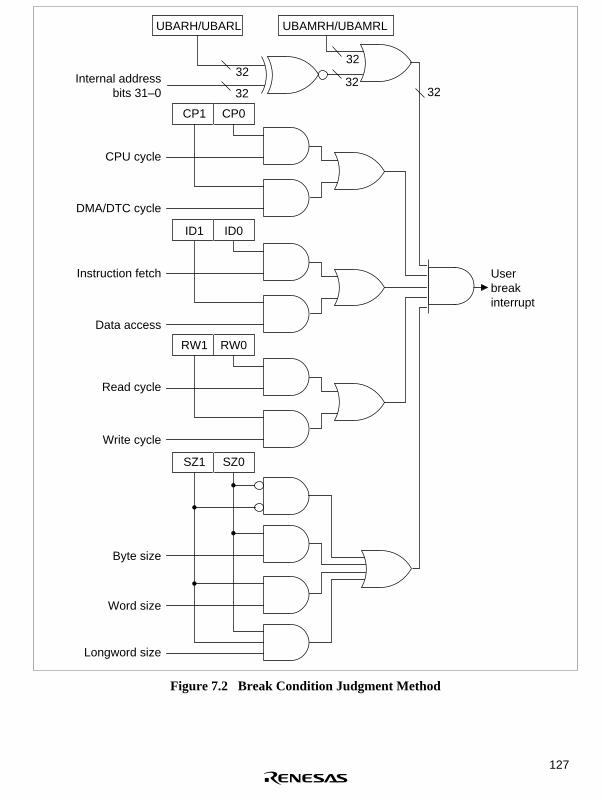
127
SZ1 SZ0
Userbreakinterrupt
RW1 RW0
ID1 ID0
CP1 CP0
UBARH/UBARL UBAMRH/UBAMRL
32
32
32
3232
Internal addressbits 31–0
CPU cycle
DMA/DTC cycle
Instruction fetch
Data access
Read cycle
Write cycle
Byte size
Word size
Longword size
Figure 7.2 Break Condition Judgment Method

128
7.3.2 Break on On-Chip Memory Instruction Fetch Cycle
On-chip memory (on-chip ROM and/or RAM) is always accessed as 32 bits in 1 bus cycle.Therefore, 2 instructions can be retrieved in 1 bus cycle when fetching instructions from on-chipmemory. At such times, only 1 bus cycle is generated, but by setting the start addresses of bothinstructions in the user break address register (UBAR) it is possible to cause independent breaks.In other words, when wanting to effect a break using the latter of two addresses retrieved in 1 buscycle, set the start address of that instruction in UBAR. The break will occur after execution of theformer instruction.
7.3.3 Program Counter (PC) Values Saved
Break on Instruction Fetch (Before Execution): The program counter (PC) value saved to thestack in user break interrupt exception processing is the address that matches the break condition.The user break interrupt is generated before the fetched instruction is executed. If a breakcondition is set in an instruction fetch cycle placed immediately after a delayed branch instruction(delay slot), or on an instruction that follows an interrupt-disabled instruction, however, the userbreak interrupt is not accepted immediately, but the break condition establishing instruction isexecuted. The user break interrupt is accepted after execution of the instruction that has acceptedthe interrupt. In this case, the PC value saved is the start address of the instruction that will beexecuted after the instruction that has accepted the interrupt.
Break on Data Access (CPU/Peripheral): The program counter (PC) value is the top address ofthe next instruction after the last instruction executed before the user break exception processingstarted. When data access (CPU/peripheral) is set as a break condition, the place where the breakwill occur cannot be specified exactly. The break will occur at the instruction fetched close towhere the data access that is to receive the break occurs.
7.4 Use Examples
7.4.1 Break on CPU Instruction Fetch Cycle
1. Register settings: UBARH = H'0000UBARL = H'0404UBBR = H'0054
Conditions set: Address: H'00000404Bus cycle: CPU, instruction fetch, read(operand size not included in conditions)
A user break interrupt will occur before the instruction at address H'00000404. If it is possible forthe instruction at H'00000402 to accept an interrupt, the user break exception processing will beexecuted after execution of that instruction. The instruction at H'00000404 is not executed. ThePC value saved is H'00000404.

129
2. Register settings: UBARH = H'0015UBARL = H'389CUBBR = H'0058
Conditions set: Address: H'0015389CBus cycle: CPU, instruction fetch, write(operand size not included in conditions)
A user break interrupt does not occur because the instruction fetch cycle is not a write cycle.
3. Register settings: UBARH = H'0003UBARL = H'0147UBBR = H'0054
Conditions set: Address: H'00030147Bus cycle: CPU, instruction fetch, read(operand size not included in conditions)
A user break interrupt does not occur because the instruction fetch was performed for an evenaddress. However, if the first instruction fetch address after the branch is an odd address set bythese conditions, user break interrupt exception processing will be done after address errorexception processing.
7.4.2 Break on CPU Data Access Cycle
1. Register settings: UBARH = H'0012UBARL = H'3456UBBR = H'006A
Conditions set: Address: H'00123456Bus cycle: CPU, data access, write, word
A user break interrupt occurs when word data is written into address H'00123456.
2. Register settings: UBARH = H'00A8UBARL = H'0391UBBR = H'0066
Conditions set: Address: H'00A80391Bus cycle: CPU, data access, read, word
A user break interrupt does not occur because the word access was performed on an even address.

130
7.4.3 Break on DMA/DTC Cycle
1. Register settings: UBARH = H'0076UBARL = H'BCDCUBBR = H'00A7
Conditions set: Address: H'0076BCDCBus cycle: DMA/DTC, data access, read, longword
A user break interrupt occurs when longword data is read from address H'0076BCDC.
2. Register settings: UBARH = H'0023UBARL = H'45C8UBBR = H'0094
Conditions set: Address: H'002345C8Bus cycle: DMA/DTC, instruction fetch, read(operand size not included in conditions)
A user break interrupt does not occur because no instruction fetch is performed in the DMA/DTCcycle.
7.5 Cautions on Use
7.5.1 On-Chip Memory Instruction Fetch
Two instructions are simultaneously fetched from on-chip memory. If a break condition is set onthe second of these two instructions but the contents of the UBC break condition registers arechanged so as to alter the break condition immediately after the first of the two instructions isfetched, a user break interrupt will still occur when the second instruction is fetched.
7.5.2 Instruction Fetch at Branches
When a conditional branch instruction or TRAPA instruction causes a branch, instructions arefetched and executed as follows:
1. Conditional branch instruction, branch taken: BT, BF
Instruction fetch cycles: Conditional branch instruction fetch → Next-instruction overrun fetch → Next-instruction overrun fetch → Branch destination instruction fetch
Instruction execution: Conditional branch instruction execution → Branch destination instruction execution
2. TRAPA instruction, branch taken: TRAPA
Instruction fetch cycles: TRAPA instruction fetch → Next-instruction overrun fetch → Next-instruction overrun fetch → Branch destination instruction fetch

131
Instruction execution: TRAPA instruction execution → Branch destination instruction execution
3. Conditional delay branch instruction, branch taken: BT/S, BF/S
Instruction fetch cycles: Conditional delay branch instruction fetch → Next-instruction fetch (delay slot) → Next-instruction overrun fetch → Branch destination instruction fetch
Instruction execution: Conditional delay branch instruction execution → Delay slot instruction execution → Branch destination instruction execution
When a conditional branch instruction or TRAPA instruction causes a branch, the branchdestination will be fetched after the next instruction or the one after that does an overrun fetch.However, because the instruction that is the object of the break first breaks after a definiteinstruction fetch and execution, the kind of overrun fetch instructions noted above do notbecome objects of a break. If data access breaks are also included with instruction fetch breaksas break conditions, a break occurs because the instruction overrun fetch is also regarded asbecoming a data break.
7.5.3 Contention between User Break and Exception Handling
If a user break is set for the fetch of a particular instruction, and exception handling with higherpriority than a user break is in contention and is accepted in the decode stage for that instruction(or the next instruction), user break exception handling may not be performed after completion ofthe higher-priority exception handling routine (on return by RTE).
Thus, if a user break condition has been set for the fetch of the branch destination instructionfollowing a branch (BRA, BRAF, BT, BF, BT/S, BF/S, BSR, BSRF, JMP, JSR, RTS, RTE,exception handling), and exception handling for this branch destination instruction with a higherpriority than a user break interrupt is accepted, user break exception handling will not beperformed after completion of that exception handling routine.
Therefore, a user break condition must not be set for the fetch of the branch destination instructionfollowing a branch.
7.5.4 Break at Non-Delay Branch Instruction Jump Destination
When a branch instruction with no delay slot (including exception handling) jumps to the jumpdestination instruction on execution of the branch, a user break will not be generated even if a userbreak condition has been set for the first jump destination instruction fetch.

132

133
Section 8 Data Transfer Controller (DTC)
8.1 Overview
The SH7040 Series has an on-chip data transfer controller (DTC), which is activated either byinterrupts or software and can perform data transfers.
8.1.1 Features
• Arbitrary channel number transfer setting possible
Transfer information can be established for each interrupt source
Transfer information stored in memory
Multiple data transfers possible (chain transfers) for one activating source
• Address space: 32-bit addresses can be designated for both transfer source and destination
• Transfer devices
Memory: On-chip ROM, on-chip RAM, external ROM, external RAM
On-chip peripheral modules (excluding DMAC/DTC)
Memory-mapped external devices
• Abundant transfer modes
Can select between normal mode/repeat mode/block transfer mode
Can select between increment/decrement/fixed for source/destination address
• Transfer units can be set as byte/word/longword
• Interrupts activating the DTC can be requested of the CPU
Interrupt requests can be generated to the CPU after completion of a data transfer
Interrupt requests generated to the CPU after completion of all designated data transfers
• Transfers can be activated by software
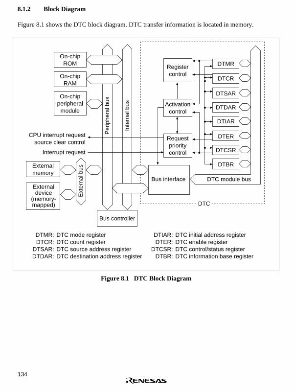
134
8.1.2 Block Diagram
Figure 8.1 shows the DTC block diagram. DTC transfer information is located in memory.
CPU interrupt requestsource clear control
Interrupt request
DTC
On-chipROM
On-chipRAM
On-chipperipheral
moduleP
erip
hera
l bus
Ext
erna
l busExternal
memory
Bus controller
Registercontrol
Activationcontrol
Requestprioritycontrol
Bus interface DTC module bus
DTMR
DTCR
DTSAR
DTDAR
DTIAR
DTER
DTCSR
DTBR
Inte
rnal
bus
DTMR:DTCR:
DTSAR:DTDAR:
DTC mode registerDTC count registerDTC source address registerDTC destination address register
DTIAR:DTER:
DTCSR:DTBR:
DTC initial address registerDTC enable registerDTC control/status registerDTC information base register
Externaldevice
(memory-mapped)
Figure 8.1 DTC Block Diagram

135
8.1.3 Register Configuration
The DTC has five registers in memory used for storing transfer data: DTMR, DTCR, DTSAR,DTDAR, and DTIAR. It is controlled by the three registers DTER (DTEA–DTEE), DTCSR, andDTBR. The register configurations are listed in table 8.1.
Table 8.1 Register Configuration* 1
Name Abbr. R/W Initial Value Address Access Size
DTC mode register DTMR —* 2 Undefined —* 2 —* 2
DTC source address register DTSAR —* 2 Undefined —* 2 —* 2
DTC destination address register DTDAR —* 2 Undefined —* 2 —* 2
DTC initial address register DTIAR —* 2 Undefined —* 2 —* 2
DTC transfer count register A DTCRA —* 2 Undefined —* 2 —* 2
DTC transfer count register B DTCRB —* 2 Undefined —* 2 —* 2
DTC enable register A DTEA R/W H'00 H'FFFF8700 8, 16, 32
DTC enable register B DTEB R/W H'00 H'FFFF8701 8, 16, 32
DTC enable register C DTEC R/W H'00 H'FFFF8702 8, 16, 32
DTC enable register D DTED R/W H'00 H'FFFF8703 8, 16, 32
DTC enable register E DTEE R/W H'00 H'FFFF8704 8, 16, 32
DTC control/status register DTCSR R/(W)* 3 H'0000 H'FFFF8706 8, 16, 32
DTC information base register DTBR R/W Undefined H'FFFF8708 16, 32
Notes: * 1 DTC registers cannot be accessed by DMAC/DTC.* 2 DTC internal registers cannot be directly accessed.* 3 Only a 0 write after a 1 read is possible for the NMIF, AE bits of the DTCSR.
8.2 Register Description
8.2.1 DTC Mode Register (DTMR)
The DTC mode register (DTMR) is a 16-bit register that controls the DTC operation mode. Thecontents of this register is located in memory.

136
Bit: 15 14 13 12 11 10 9 8
SM1 SM0 DM1 DM0 MD1 MD0 SZ1 SZ0
Initial value: * * * * * * * *
R/W: — — — — — — — —
Bit: 7 6 5 4 3 2 1 0
Bit name: DTS CHNE DISEL NMIM — — — —
Initial value: * * * * * * * *
R/W: — — — — — — — —
Note: * Initial value undefined.
• Bits 15–14—Source Address Mode 1, 0 (SM1, SM0): These bits designate whether to hold,increment, or decrement the DTSAR after a data transfer.
Bit 15 (SM1) Bit 14 (SM0) Description
0 — DTSAR remains fixed
1 0 DTSAR is incremented after transfer
(+1 for byte unit transfer, +2 for word, +4 for longword)
1 1 DTSAR is decremented after transfer
(–1 for byte unit transfer, –2 for word, –4 for longword)
• Bits 13–12—Destination Address Mode 1, 0 (DM1, DM0): These bits designate whether tohold, increment or decrement the DTDAR after a data transfer.
Bit 13 (DM1) Bit 12 (DM0) Description
0 — DTDAR remains fixed
1 0 DTDAR is incremented after transfer
(+1 for byte unit transfer, +2 for word, +4 for longword)
1 1 DTDAR is decremented after transfer
(–1 for byte unit transfer, –2 for word, –4 for longword)

137
• Bits 11–10—DTC Mode 1, 0 (MD1, MD0): These bits designate the DTC transfer mode.
Bit 11 (MD1) Bit 10 (MD0) Description
0 0 Normal mode
0 1 Repeat mode
1 0 Block transfer mode
1 1 Reserved (setting prohibited)
• Bits 9–8—DTC Data Transfer Size 1, 0 (SZ1, SZ0): These bits designate the data size for datatransfers.
Bit 9 (SZ1) Bit 8 (SZ0) Description
0 0 Byte (8 bits)
0 1 Word (16 bits)
1 0 Longword (32 bits)
1 1 Reserved (setting prohibited)
• Bit 7—DTC Transfer Mode Select (DTS): When in repeat mode or block transfer mode, thisbit designates whether the source side or destination side will be the repeat area or block area.
Bit 7 (DTS) Description
0 Destination side is the repeat area or block area
1 Source side is the repeat area or block area
• Bit 6—DTC Chain Enable (CHNE): This bit designates whether to perform continuous DTCdata transfers with the same activating source. Continued transfer information is read after the16th byte from the start address of the previous transfer information.
Bit 6 (CHNE) Description
0 DTC data transfer end (activation wait state ensues)
1 DTC data transfer continue (read continue register information, executetransfer)

138
• Bit 5—DTC Interrupt Select (DISEL): This bit designates whether to prohibit or allowinterrupt requests to the CPU after one-time DTC transfers.
Bit 5 (DISEL) Description
0 Prohibit interrupts to the CPU after DTC data transfer completion if thetransfer counter is not 0 (DTC clears the interrupt source flag of theactivating source to 0)
1 Allow interrupts to the CPU after DTC data transfer completion (DTCclears the DTER bit for the interrupt of the activating source to 0)
• Bit 4—DTC NMI Mode (NMIM): This bit designates whether to terminate transfers when anNMI is input during DTC transfers.
Bit 4 (NMIM) Description
0 Terminate DTC transfer upon an NMI
1 Continue DTC transfer until end of transfer being executed
• Bits 3–0—Reserved: They have no effect on DTC operation.
8.2.2 DTC Source Address Register (DTSAR)
The DTC source address register (DTSAR) is a 32-bit register that specifies the DTC transfersource address. An even address indicates that the transfer size is word; a multiple-of-four addressmeans it is longword. The contents of this register is located in memory.
Bit: 31 30 29 28 27 … 4 3 2 1 0
…
Initial value: * * * * * … * * * * *
R/W: — — — — — … — — — — —
Note: * Initial value is undefined.
8.2.3 DTC Destination Address Register (DTDAR)
The DTC destination address register (DTDAR) is a 32-bit register that specifies the DTC transferdestination address. An even address indicates that the transfer size is word; a multiple-of-fouraddress means it is longword. The contents of this register are located in memory.

139
Bit: 31 30 29 28 27 … 4 3 2 1 0
…
Initial value: * * * * * … * * * * *
R/W: — — — — — … — — — — —
Note: * Initial value is undefined.
8.2.4 DTC Initial Address Register (DTIAR)
The DTC initial address register (DTIAR) specifies the initial transfer source/transfer destinationaddress in repeat mode. In repeat mode, when the DTS bit is set to 1, specify the initial transfersource address in the repeat area, and when the DTS bit is cleared to 0, specify the initial transferdestination address in the repeat area.
The contents of this register are located in memory.
Bit: 31 30 29 28 27 … 4 3 2 1 0
…
Initial value: * * * * * … * * * * *
R/W: — — — — — … — — — — —
Note: * Initial value is undefined.
8.2.5 DTC Transfer Count Register A (DTCRA)
DTCRA is a 16-bit register that specifies the number of DTC transfers. The contents of thisregister are located in memory.
In normal mode it functions as a 16-bit transfer counter. The number of transfers is 1 when the setvalue is H'0001, 65535 when it is H'FFFF, and 65536 when it is H'0000.
In repeat mode, DTCRAH maintains the transfer count and DTCRAL functions as an 8-bittransfer counter. The number of transfers is 1 when the set value is DTCRAH = DTCRAL = H'01,255 when they are H'FF, and 256 when it is H'00.
In block transfer mode it functions as a 16-bit transfer counter. The number of transfers is 1 whenthe set value is H'0001, 65535 when it is H'FFFF, and 65536 when it is H'0000.

140
Bit: 15 14 8
DTCRAH
Initial value: * * * * * * * *
R/W: — — — — — — — —
Bit: 7 6 0
DTCRAL
Initial value: * * * * * * * *
R/W: — — — — — — — —
Note: * Initial value is undefined.
8.2.6 DTC Transfer Count Register B (DTCRB)
The DTCRB is a 16-bit register that designates the block length in block transfer mode. Thecontents of this register is located in memory. The block length is 1 when the set value is H'0001,65535 when it is H'FFFF, and 65536 when it is H'0000.
Bit: 15 14 13 12 11 10 9 8
Initial value: * * * * * * * *
R/W: — — — — — — — —
Bit: 7 6 5 4 3 2 1 0
Initial value: * * * * * * * *
R/W: — — — — — — — —
Note: * Initial value is undefined.
8.2.7 DTC Enable Registers (DTER)
The DTER (DTEA–DTEE) are five 8-bit readable/writable registers with bits allocated to eachinterrupt source that activates the DTC. They set disable/enable for DTC activation for eachinterrupt source. When a bit is 1, DTC activation by the corresponding interrupt source is enabled.Interrupt sources for each of the DTEA–DTEE registers are indicated in table 8.2.
The DTER are initialized to H'00 by a power-on reset or in standby mode. Manual reset does notinitialize DTER.

141
For the A mask, overwrite this register as follows:
When clearing bit to 0: read the 1 bit to clear and write 0.When setting bit to 1: read the 0 bit to set and write 1.
Bit: 7 6 5 4 3 2 1 0
DTE7 DTE6 DTE5 DTE4 DTE3 DTE2 DTE1 DTE0
Initial value: 0 0 0 0 0 0 0 0
R/W: R/W* R/W* R/W* R/W* R/W* R/W* R/W* R/W*
Note: * DTER bits can only be modified by writing 1 after reading 0, or writing 0 after reading 1.
8.2.8 DTC Control/Status Register (DTCSR)
The DTCSR is a 16-bit readable/writable register that sets disable/enable for DTC activation bysoftware, as well as the DTC vector addresses for software activation. It also indicates the DTCtransfer status.
The DTCSR is initialized to H'0000 by power-on resets and in standby mode. Manual reset doesnot initialize DTCSR.
Bit: 15 14 13 12 11 10 9 8
— — — — — NMIF AE SWDTE
Initial value: 0 0 0 0 0 0 0 0
R/W: R R R R R R/W* 1 R/W* 1 R/W* 2
Bit: 7 6 5 4 3 2 1 0
Bit name: DTVEC7 DTVEC6 DTVEC5 DTVEC4 DTVEC3 DTVEC2 DTVEC1 DTVEC0
Initial value: 0 0 0 0 0 0 0 0
R/W: R/W* 3 R/W* 3 R/W* 3 R/W* 3 R/W* 3 R/W* 3 R/W* 3 R/W* 3 * 4
Notes: * 1 For the NMIF and AE bits, only a 0 write after a 1 read is possible.* 2 For the SWDTE bit, a 1 write is always possible, but a 0 write is possible only after a 1
is read.* 3 For the DTVEC7–DTVEC0 bits, writes are possible only when SWDTE = 0.* 4 Be sure to write 0 to the DTVEC0 bit.
Bits 15–11—Reserved: These bits always read as 0. The write value should always be 0.

142
• Bit 10—NMI Flag Bit (NMIF): Indicates that an NMI interrupt has occurred. When the NMIFbit is set, DTC transfers are not allowed even if the DTER bit is set to 1. If, however, a transferhas already started with the NMIM bit of the DTMR set to 1, execution will continue until thattransfer ends. To clear the NMIF bit, read the 1 from it, then write a 0.
The NMIF bit is initialized to 0 by power-on resets and in standby mode.
Bit 10 (NMIF) Description
0 No NMI interrupts (initial value)
(Clear condition) Write a 0 after reading the NMIF bit
1 NMI interrupt has been generated
• Bit 9—Address Error Flag (AE): Indicates that an address error by the DTC has occurred.When the AE bit is set, DTC transfers are not allowed even if the DTER bit is set to 1. To clearthe AE bit, read the 1 from it, then write a 0.
The AE bit is initialized to 0 by power-on resets and in standby mode.
Bit 9 (AE) Description
0 No address error by the DTC (initial value)
(Clear condition) Write a 0 after reading the AE bit
1 An address error by the DTC occurred
• Bit 8—DTC Software Activation Enable Bit (SWDTE): This bit enables/disables DTCactivation by software.
The AE bit is initialized to 0 by resets and standby mode. For details, see section 8.3.2,Activating Sources.
Bit 8 (SWDTE) Description
0 DTC activation by software disabled (initial value)
1 DTC activation by software enabled
• Bits 7–0—Software Activation Vectors 7–0 (DTVEC7–DTVEC0): These bits set the DTCvector addresses for DTC activation by software. A vector address is calculated as H'0400 +DTVEC[7:0]. Always specify 0 for DTVEC0. 8 bits are available, so you can specify valuesH'00 (0)–H'FE (254).

143
8.2.9 DTC Information Base Register (DTBR)
The DTBR is a 16-bit readable/writable register that specifies the upper 16 bits of the memoryaddress containing DTC transfer information. Always access the DTBR in word or longwordunits. If it is accessed in byte units the register contents will become undefined at the time of awrite, and undefined values will be read out upon reads.
The DTBR is not initialized either by resets or in standby mode.
Bit: 15 14 13 12 11 10 9 8
Initial value: * * * * * * * *
R/W: R/W R/W R/W R/W R/W R/W R/W R/W
Bit: 7 6 5 4 3 2 1 0
Initial value: * * * * * * * *
R/W: R/W R/W R/W R/W R/W R/W R/W R/W
Note: * Initial value is undefined.
8.3 Operation
The DTC stores transfer information in memory. When there are DTC transfer requests, it readsthat transfer information and performs data transfers based on it. It rewrites the transferinformation to memory after data transfers. Storing transfer information in memory makes itpossible to perform data transfers for an arbitrary number of channels. Further, setting the CHNEbit to 1 makes it possible to perform multiple transfers continuously through one DTC transferrequest.
There are three DTC transfer modes: normal mode, repeat mode, and block transfer mode. After aDTC transfer, the transfer source address and transfer destination address are incremented,decremented, or kept the same, according to the respective setting.
8.3.1 Overview of Operation
Figure 8.2 shows a flowchart of DTC operation.

144
Yes
No
Yes
Yes
Yes
Yes
No
No
No
No
Start
Initial settingsDTMR, DTCR, DTIAR, DTSAR, DTDAR
Transfer requestgenerated?
NMIF = AE = 0?
DTC vector read
Transfer information read
DTCRA = DTCRA – 1 (normal/block transfer mode)DTCRAL = DTCRAL – 1 (repeat mode)
DTSAR, DTDAR updateDTCRB = DTCRB – 1 (block transfer mode)
Transfer (1 transfer unit)
Blocktransfer mode and
DTCRB ≠ 0?
Transfer information write
NMI or address error
End
Transfer information write
CHNE = 0?
NMIF • NMIM+ AE = 1?
When DISEL = 1 or DTCRA = 0 (normal/block transfer mode)When DISEL = 1 (repeat transfer mode)
CPU interrupt request
Figure 8.2 DTC Operation Flowchart

145
8.3.2 Activating Sources
The DTC performs write operations to the DTCSR with either interrupt sources or software as itsactivating sources. Each interrupt source is designated by specific DTER bits to determine whetherit becomes an interrupt request to the CPU or a DTC activating source.
When the DISEL bit is 1, an interrupt, established as the DTC activating source, is requested ofthe CPU after each data transfer in DRC. When the DISEL bit is a 0, a request is made only afterthe completion of a designated number of data transfers. When the activating source interrupt isrequested of the CPU, the corresponding DTER bit is automatically cleared.
In the case of software activation also, when the DISEL bit is a 1, a software DTC activationinterrupt (SWDTCE) is requested of the CPU after each data transfer. When the DISEL bit is a 0,a request is made only after the completion of a designated number of data transfers. When noSWDTCE interrupt is requested of the CPU, the SWDTE bit of the DTCSR is automaticallycleared. When a request is made of the CPU, the SWDTE bit is maintained as a 1.
When multiple DTC activating sources occur simultaneously, they are accepted and the DTC isactivated in accordance with the default priority rankings shown in table 8.2.
Figure 8.3 shows a block diagram of activating source control.
IRQOn-chip
peripheral
Interrupt requests
Source
flag clear
Source flag clear
Interrupt requests (those not designated as DMAC activating sources)
CPU Interrupt requests (those not designated as DTC activating sources)
Clear
DTC activation request
DTC control
DTER
DTC
INTC
DMAC
Figure 8.3 Activating Source Control Block Diagram
8.3.3 DTC Vector Table
Figure 8.4 shows the correspondence between DTC vector addresses and register informationplacement. For each DTC activating source there are 2 bytes in the DTC vector table, whichcontain the register information start address.
Table 8.2 shows the correspondence between activating sources and vector addresses. Whenactivating with software, the vector address is calculated as H'0400 + DTVEC[7:0].

146
Through DTC activation, a register information start address is read from the vector table, thenregister information placed in memory space is read from that register information start address.Always designate register information start addresses in multiples of four.
Register information start address
DTBR
(upper 16 bits)
Memory space
DTC vector table
Registerinformation
DTC vector address
Registerinformation
start address(lower 16 bits)
Figure 8.4 Correspondence between DTC Vector Address and Register Information

147
Table 8.2 Interrupt Sources and DTC Vector Addresses
SourceGenerator
ActivatingSource DTC Vector Address
DTEBit
TransferSource
TransferDestination Priority
MTU TGI4A H'00000400–H'00000401 DTEA7 Arbitrary* 1 Arbitrary* 1 High(CH4) TGI4B H'00000402–H'00000403 DTEA6 Arbitrary* 1 Arbitrary* 1
TGI4C H'00000404–H'00000405 DTEA5 Arbitrary* 1 Arbitrary* 1
TGI4D H'00000406–H'00000407 DTEA4 Arbitrary* 1 Arbitrary* 1
TCI4V H'00000408–H'00000409 DTEA3 Arbitrary* 1 Arbitrary* 1
MTU TGI3A H'0000040A–H'0000040B DTEA2 Arbitrary* 1 Arbitrary* 1
(CH3) TGI3B H'0000040C–H'0000040D DTEA1 Arbitrary* 1 Arbitrary* 1
TGI3C H'0000040E–H'0000040F DTEA0 Arbitrary* 1 Arbitrary* 1
TGI3D H'00000410–H'00000411 DTEB7 Arbitrary* 1 Arbitrary* 1
MTU TGI2A H'00000412–H'00000413 DTEB6 Arbitrary* 1 Arbitrary* 1
(CH2) TGI2B H'00000414–H'00000415 DTEB5 Arbitrary* 1 Arbitrary* 1
MTU TGI1A H'00000416–H'00000417 DTEB4 Arbitrary* 1 Arbitrary* 1
(CH1) TGI1B H'00000418–H'00000419 DTEB3 Arbitrary* 1 Arbitrary* 1
MTU TGI0A H'0000041A–H'0000041B DTEB2 Arbitrary* 1 Arbitrary* 1
(CH0) TGI0B H'0000041C–H'0000041D DTEB1 Arbitrary* 1 Arbitrary* 1
TGI0C H'0000041E–H'0000041F DTEB0 Arbitrary* 1 Arbitrary* 1
TGI0D H'00000420–H'00000421 DTEC7 Arbitrary* 1 Arbitrary* 1
A/D ADI(ADI0)* 2H'00000422–H'00000423 DTEC6 ADDR Arbitrary* 1
IRQ0 pin IRQ0 H'00000424–H'00000425 DTEC5 Arbitrary* 1 Arbitrary* 1
IRQ1 pin IRQ1 H'00000426–H'00000427 DTEC4 Arbitrary* 1 Arbitrary* 1
IRQ2 pin IRQ2 H'00000428–H'00000429 DTEC3 Arbitrary* 1 Arbitrary* 1
IRQ3 pin IRQ3 H'0000042A–H'0000042B DTEC2 Arbitrary* 1 Arbitrary* 1
IRQ4 pin IRQ4 H'0000042C–H'0000042D DTEC1 Arbitrary* 1 Arbitrary* 1
IRQ5 pin IRQ5 H'0000042E–H'0000042F DTEC0 Arbitrary* 1 Arbitrary* 1
IRQ6 pin IRQ6 H'00000430–H'00000431 DTED7 Arbitrary* 1 Arbitrary* 1
IRQ7 pin IRQ7 H'00000432–H'00000433 DTED6 Arbitrary* 1 Arbitrary* 1
CMT (CH0) CMI0 H'00000434–H'00000435 DTED5 Arbitrary* 1 Arbitrary* 1
CMT (CH1) CMI1 H'00000436–H'00000437 DTED4 Arbitrary* 1 Arbitrary* 1 Low

148
Table 8.2 Interrupt Sources and DTC Vector Addresses (cont)
SourceGenerator
ActivatingSource DTC Vector Address
DTEBit
TransferSource
TransferDestination Priority
SCI0 RXI0 H'00000438–H'00000439 DTED3 RDR0 Arbitrary* 1 High
TXI0 H'0000043A–H'0000043B DTED2 Arbitrary* 1 TDR0
SCI1 RXI1 H'0000043C–H'0000043D DTED1 RDR1 Arbitrary* 1
TXI1 H'0000043E–H'0000043F DTED0 Arbitrary* 1 TDR1
BSC CMI H'00000440–H'00000441 DTEE7 Arbitrary* 1 Arbitrary* 1
Software Write toDTCSR
H'00000400 + DTVEC[7:0] toH'00000401 + DTVEC[7:0]
— Arbitrary* 1 Arbitrary* 1
Low
Notes: * 1 External memory, memory-mapped external devices, on-chip memory, on-chipperipheral modules (excluding DMAC and DTC)
* 2 Excluding A mask products are ADI, A mask products are ADI0.
8.3.4 Register Information Placement
Figure 8.5 shows the placement of register information in memory space. The register informationstart addresses are designated by DTBR for the upper 16 bits, and the DTC vector table for thelower 16 bits.
The placement in order from the register information start address in normal mode is DTMR,DTCRA, 4 bytes empty (no effect on DTC operation), DTSAR, then DTDAR. In repeat mode it isDTMR, DTCRA, DTIAR, DTSAR, and DTDAR. In block transfer mode, it is DTMR, DTCRA, 2bytes empty (no effect on DTC operation), DTCRB, DTSAR, then DTDAR.
Fundamentally, certain RAM areas are designated for addresses storing register information.

149
Registerinformation
start address
Memory space Memory space Memory space
Registerinformation
Normal mode Repeat mode
Block transfer mode
DTMRDTCRA
DTSAR
DTDAR
DTMRDTCRA
DTSAR
DTDAR
DTIAR
DTMRDTCRA
DTSAR
DTDAR
DTCRB
Figure 8.5 DTC Register Information Placement in Memory Space
8.3.5 Normal Mode
Performs the transfer of one byte, one word, or one longword for each activation. The totaltransfer count is 1 to 65536. An interrupt request is generated to the CPU when the transfer withDTCRA = 1 ends. Transfers of a number of bytes specified by the SCI are possible.
Table 8.3 shows the register functions for normal mode.
Table 8.3 Normal Mode Register Functions
Values Written Back upon aTransfer Information Write
Register FunctionWhen DTCRAis other than 1 When DTCRA is 1
DTMR Operation modecontrol
DTMR DTMR
DTCRA Transfer count DTCRA – 1 DTCRA – 1 (= H'0000)
DTSAR Transfer sourceaddress
Increment/decrement/fixed
Increment/decrement/fixed
DTDAR Transfer destinationaddress
Increment/decrement/fixed
Increment/decrement/fixed
8.3.6 Repeat Mode
Performs the transfer of one byte, one word, or one longword for each activation. Either thetransfer source or transfer destination is designated as the repeat area.

150
The total transfer count is specified between 1 and 256. When the specified number of transfersends, the address register of the designated repeat area is returned to its initial state and the transferis repeated. Other address registers are consecutively incremented, decremented, or remain fixed.While DISEL = 0, no interrupt request is made to the CPU, even if the transfer with DTCRAL = 1ends.
Pulses for driving the stepping motor can be output. Table 8.4 shows the register functions forrepeat mode.
Table 8.4 Repeat Mode Register Functions
Values Written Back upon aTransfer Information Write
Register FunctionWhen DTCRA isother than 1 When DTCRA is 1
DTMR Operation modecontrol
DTMR DTMR
DTCRAH Transfer countmaintenance
DTCRAH DTCRAH
DTCRAL Transfer count DTCRAL – 1 DTCRAH
DTIAR Initial address (Not written back) (Not written back)
DTSAR Transfer sourceaddress
Increment/decrement/fixed
(DTS = 0) Increment/decrement/ fixed
(DTS = 1) DTIAR
DTDAR Transfer destinationaddress
Increment/decrement/fixed
(DTS = 0) DTIAR
(DTS = 1) Increment/decrement/ fixed
8.3.7 Block Transfer Mode
Performs the transfer of one block for each one activation. Either the transfer source or transferdestination is designated as the block area.
The block length is specified between 1 and 65536. When a 1-block transfers ends, the addressregister of the designated block area is returned to its initial state. Other address registers areconsecutively incremented, decremented, or remain fixed. The block transfer count is 1 to 65536.An interrupt request is generated to the CPU when the transfer with DTCRA = 1 ends.
A/D converter group mode transfers and phase compensation PWM data transfers are possible.
Table 8.5 shows the register functions for block transfer mode.

151
Table 8.5 Block Transfer Mode Register Functions
Register FunctionValues Written Back upon aTransfer Information Write
DTMR Operation modecontrol
DTMR
DTCRA Transfer count DTCRA – 1
DTCRB Block length (Not written back)
DTSAR Transfer sourceaddress
(DTS = 0) Increment/ decrement/ fixed
(DTS = 1) DTSAR initial value
DTDAR Transfer destinationaddress
(DTS = 0) DTDAR initial value
(DTS = 1) Increment/ decrement/ fixed
8.3.8 Operation Timing
Figure 8.6 shows a DTC operation timing example.
Activatingsource
DTCrequest
Address
Vectorread
Datatransfer
Transferinformation
read
Transferinformation
write
R W
φ
Figure 8.6 DTC Operation Timing Example (Normal Mode)
When register information is located in on-chip RAM, each mode requires 4 cycles for transferinformation reads, and 3 cycles for writes.
8.3.9 DTC Execution State Counts
Table 8.6 shows the execution state for one DTC data transfer. Furthermore, table 8.7 shows thestate counts needed for execution state.

152
Table 8.6 Execution State of DTC
Mode Vector Read I
RegisterInformationRead/Write J Data Read K Data Write L
InternalOperation M
Normal 1 7 1 1 1
Repeat 1 7 1 1 1
Block transfer 1 7 N N 1
Note: N: block size (default set values of DTCRB)
Table 8.7 State Counts Needed for Execution State
Access Objective
On-chipRAM
On-chipROM
Internal I/ORegister External Device
Bus width 32 32 32 8 16 32
Accessstate
1 1 2* 1 3* 2 2 2 2
Execution Vector read SI — 1 — 4 2 2state Register information
read/writeSJ 1 1 — 8 4 2
Byte data read SK 1 1 2 3 2 2 2
Word data read SK 1 1 2 3 4 2 2
Long word data read SK 1 1 4 6 8 4 2
Byte data write SL 1 1 2 3 2 2 2
Word data write SL 1 1 2 3 4 2 2
Long word write SL 1 1 4 6 8 4 2
Internal operation SM 1
Notes: * 1 Two state access module : port, INT, CMT, SCI, etc.* 2 Three state access module : WDT, CACHE, UBC, etc.
The execution state count is calculated using the following formula. ∑ indicates the number oftransfers by one activating source (count + 1 when CHNE bit is 1).
Execution state count = I · SI + ∑ (J · SJ + K · SK + L · SL) + M · SM

153
8.3.10 DTC Usage Procedure
The procedure for DTC interrupt activation is as follows:
1. Transfer data (DTMR, DTCRA, DTSAR, DTDAR, DTCRB, and DTIAR) is located inmemory space.
2. Establish the register information start address with DTBR and the DTC vector table.
3. Set the corresponding DTER bit to 1.
4. The DTC is activated when an interrupt source occurs.
5. When interrupt requests are not made to the CPU, the interrupt source is cleared, but the DTERis not. When interrupts are requested, the interrupt source is not cleared, but the DTER is.
6. Interrupt sources are cleared within the CPU interrupt routine. When doing continuous DTCdata transfers, set the DTER to 1.
The procedure for DTC software activation is as follows:
1. Transfer data (DTMR, DTCRA, DTSAR, DTDAR, DTCRB, and DTIAR) is located inmemory space.
2. Establish the register information start address with DTBR and the DTC vector table.
3. Confirm that the SWDTE bit of the DTCSR is 0. When the SWDTE bit is 1, the DTC isalready being driven by software.
4. Write a 1 to the SWDTE bit and a vector number to the DTVEC (byte data).
5. When SWDTCE interrupt requests are not made to the CPU, the SWDTE bit is cleared. Wheninterrupts are requested, the SWDTE bit is maintained as a 1.
6. The SWDTE bit is cleared to 0 within the CPU interrupt routine. For continuous DTC datatransfers, set the SWDTE to 1.
8.3.11 DTC Use Example
The following is a DTC use example of a 128-byte data reception by the SCI:
1. The settings are: DTMR source address fixed (SM1 = 0), destination address incremented(DM1 = 1, DM0 = 0), normal mode (MD1 = MD0 = 0), byte size (SZ1 = SZ0 = 0), onetransfer per activating source (CHNE = 0), and a CPU interrupt request after the designatednumber of data transfers (DISEL = 0). 128 (H'0080) is set in DTCRA, the RDR address of theSCI is set in DTSAR, and the start address of the RAM storing the receive data is set inDTDAR.
2. Establish the register information start address with DTBR and the DTC vector table.
3. Set the corresponding DTER bit to 1.
4. Set the SCI to a specific receive mode and enable RxI interrupts.

154
5. The RDRF flag of the SSR is set to 1 by each completion of a 1-byte data reception by the SCI,an RxI interrupt is generated, and the DTC is activated. The received data is transferred fromRDR to RAM by the DTC, and the RDRF flag is 0 cleared.
6. After completion of 128 data transfers (DTCRA = 0), the DTER is cleared while the RDRF ismaintained as 1, and an RxI interrupt request is made to the CPU. The interrupt processingroutine clears the RDRF, and performs the other completion processing.
8.4 Cautions on Use
• DMAC and DTC register access by the DTC is prohibited.
• DTC register access by the DMAC is prohibited.
• When setting a bit in DTER, first ensure that all transfers on the DTC channel corresponding tothat DTER have ended, or disable the transfer source for each channel so that DTC transfercorresponding to that DTER will not occur. The above restrictions do not apply for A mask due to change in the access method of DTER. However, take caution when changing LSI to A mask, since modification of the program is required.

155
Section 9 Cache Memory (CAC)
9.1 Overview
The LSI has an on-chip cache memory (CAC) with 1 kbyte of cache data and a 256-entry cachetag. The cache data and cache tag space can be used as on-chip RAM space when the cache is notbeing used.
9.1.1 Features
The CAC has the following features. The cache tag and cache data configuration is shown infigure 9.1.
• 1-kbyte capacity
• External memory (CS space and DRAM space) instruction code and PC relative data caching
• 256 entry cache tag (tag address 15 bits)
• 4-byte line length
• Direct map replacement algorithm
• Valid flag (1 bit) included for purges
Cache tag
256 entries
Data (32 bits)
Tag address (15 bits)
Cache data
Data bus
Hit signal
CPU address
Tag address
Entry address Offset
Valid bit (1 bit)
CMP
15 8 2
Figure 9.1 Cache Tag and Cache Data Configuration
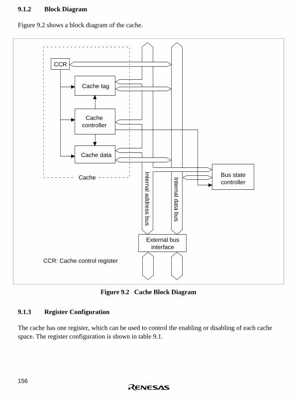
156
9.1.2 Block Diagram
Figure 9.2 shows a block diagram of the cache.
CCR: Cache control register
Cache tag
Cachecontroller
Cache data
Internal address bus
Internal data bus
Bus statecontroller
External businterface
CCR
Cache
Figure 9.2 Cache Block Diagram
9.1.3 Register Configuration
The cache has one register, which can be used to control the enabling or disabling of each cachespace. The register configuration is shown in table 9.1.

157
Table 9.1 Register Configuration
Name Abbreviation R/WInitialValue Address
Access Size(Bits)
Cache control register CCR R/W H'0000* H'FFFF8740 8, 16, 32
Note: * Bits 15–5 are undefined.
9.2 Register Explanation
9.2.1 Cache Control Register (CCR)
The cache control register (CCR) selects the cache enable/disable of each space.
The CCR is a 16-bit readable/writable register. It is initialized to H'0000 by power on resets, but isnot initialized by manual resets or standby mode.
Bit: 15 14 13 12 11 10 9 8
— — — — — — — —
Initial value: * * * * * * * *
R/W: R R R R R R R R
Bit: 7 6 5 4 3 2 1 0
— — — CEDRAM
CECS3
CECS2
CECS1
CECS0
Initial value: * * * 0 0 0 0 0
R/W: R R R R/W R/W R/W R/W R/W
Note: * Bits 15–5 are undefined.
• Bits 15–5—Reserved: Reading these bits gives undefined values. The write value shouldalways be 0.
• Bit 4—DRAM Space Cache Enable (CEDRAM): Selects whether to use DRAM space as acache object (enable) or to exclude it (disable). A 0 disables, and a 1 enables such use.
Bit 4 (CEDRAM) Description
0 DRAM space cache disabled (initial value)
1 DRAM space cache enabled

158
• Bit 3—CS3 Space Cache Enable (CECS3): Selects whether to use CS3 space as a cache object(enable) or to exclude it (disable). A 0 disables, and a 1 enables such use.
Bit 3 (CECS3) Description
0 CS3 space cache disabled (initial value)
1 CS3 space cache enabled
• Bit 2—CS2 Space Cache Enable (CECS2): Selects whether to use CS2 space as a cache object(enable) or to exclude it (disable). A 0 disables, and a 1 enables such use.
Bit 2 (CECS2) Description
0 CS2 space cache disabled (initial value)
1 CS2 space cache enabled
• Bit 1—CS1 Space Cache Enable (CECS1): Selects whether to use CS1 space as a cache object(enable) or to exclude it (disable). A 0 disables, and a 1 enables such use.
Bit 1 (CECS1) Description
0 CS1 space cache disabled (initial value)
1 CS1 space cache enabled
• Bit 0—CS0 Space Cache Enable (CECS0): Selects whether to use CS0 space as a cache object(enable) or to exclude it (disable). A 0 disables, and a 1 enables such use.
Bit 0 (CECS0) Description
0 CS0 space cache disabled (initial value)
1 CS0 space cache enabled
9.3 Address Array and Data Array
There is a special cache space for controlling the cache. This space is divided into an address arrayand a data array, where addresses (tag address, including valid bit) and data (4-byte line length) forcache control are recorded. The special cache space is shown in table 9.2. It can be used as on-chipRAM space when the cache is not being used.

159
Table 9.2 Special Cache Space
Space Classification Address Size Bus Width
Address array H'FFFFF000–H'FFFFF3FF 1 kbyte 32 bit
Data array H'FFFFF400–H'FFFFF7FF 1 kbyte 32 bit
9.3.1 Cache Address Array Read/Write Space
The cache address array has a compulsory read/write (figure 9.3).
AddressUpper 22 bits of the address array space address
(22 bits)–
(2 bits)Entry address
(8 bits)
31 02 110 9
Data–
(6 bits)–
(10 bits)Tag address
(15 bits)
Valid bit (1 bit)
31 010 926 25 24
Figure 9.3 Cache Address Array
Address Array Read: Designates entry address and reads out the corresponding tag addressvalue/valid bit value.
Address Array Write: Designates entry address and writes the designated tag address value/validbit value.
9.3.2 Cache Data Array Read/Write Space
The cache data array has a compulsory read/write (figure 9.4).
AddressUpper 22 bits of the data array space address
(22 bits)–
(2 bits)Entry address
(8 bits)
31 02 110 9
DataData
(32 bits)
31 0
Figure 9.4 Cache Data Array
Data Array Read: Designates entry address and reads out the corresponding line of data.
Data Array Write: Designates entry address and writes designated data to the corresponding line.

160
9.4 Cautions on Use
9.4.1 Cache Initialization
Always initialize the cache before enabling it. Specifically, use an address array write to write 0 toall valid bits for all entries (256 times), that is,those in the address range H'FFFFF000–H'FFFFF3FF.
Writes to the address array or data array by the CPU, DMAC, or DTC are not possible while thecache is enabled. For reads, undefined values will be read out.
9.4.2 Forced Access to Address Array and Data Array
While the cache is enabled, it is not possible to write to the address array or data array via theCPU, DMAC, or DTC, and a read will return an undefined value. The cache must be disabledbefore making a forced access to the address array or data array.
9.4.3 Cache Miss Penalty and Cache Fill Timing
When a cache miss occurs, a single idle cycle is generated as a penalty immediately before thecache fill (access from external memory in the event of a cache miss), as shown in figure 9.5.However, in the case of consecutive cache misses, idle cycles are not generated for the second andsubsequent cache misses, as shown in figure 9.6.
As the timing for a cache fill from normal space, the CS assert period immediately before the endof the bus cycle (or the last bus cycle when two or four bus cycles are generated, such as in a wordaccess to 8-bit space) is extended by an additional cycle, as shown in figures 9.5 and 9.6.
Similarly, as the timing for a cache fill from DRAM space, the RAS assert period immediatelybefore the end of the bus cycle is extended by an additional cycle. In RAS down mode, the nextbus cycle is delayed by one cycle as shown in figure 9.8.

161
Miss-hit
CK
Internaladdress
Address
CSn
RD
Data
Idle cycle
Idle cycle
Idle cycle
CS assert extension
Figure 9.5 Cache Fill Timing in Case of Non-Consecutive Cache Miss from Normal Space(No Wait, No CS Assert Extension)
Miss-hit
CK
Internaladdress
Address
CSn
RD
Data
CS assert additional extension
Figure 9.6 Cache Fill Timing in Case of Consecutive Cache Misses from Normal Space(No Wait, CS Assert Extension)

162
Idle cycle
Idle cycle
Idle cycle
CK
Internaladdress
Address
RAS
CASxx
Data
ROW COLUMN
Miss-hit
RAS assert extension
Figure 9.7 Cache Fill Timing in Case of Non-Consecutive Cache Miss from DRAM Space(Normal Mode, TPC = 0, RCD = 0, No Wait)
Miss-hit
ROW COLUMN CS spaceWait COLUMN
RAS assert extension
CK
Internaladdress
Address
RAS
CASxx
Data
DRAM accessCS spaceaccess DRAM access
Miss-hit
Figure 9.8 Cache Fill Timing in Case of Consecutive Cache Misses from DRAM Space(RAS Down Mode, TPC = 0, RCD = 0, No Wait)
9.4.4 Cache Hit after Cache Miss
The first cache hit after a cache miss is regarded as a cache miss, and a cache fill without idlecycle generation is performed. The next hit operates as a cache hit.

163
Section 10 Bus State Controller (BSC)
10.1 Overview
The bus state controller (BSC) divides up the address spaces and outputs control for various typesof memory. This enables memories like DRAM, SRAM, and ROM to be linked directly to the LSIwithout external circuitry.
10.1.1 Features
The BSC has the following features:
• Address space is divided into five spaces
A maximum linear 2 Mbytes for on-chip ROM effective mode, and a maximum linear4-Mbyte for on-chip ROM ineffective mode for address space CS0
A maximum linear 4 Mbytes for each of the address spaces CS1–CS3
A maximum linear 16 Mbytes for DRAM dedicated space
Bus width can be selected for each space (8, 16, or 32 bits)
Wait states can be inserted by software for each space
Wait states can be inserted via the WAIT pin in external memory spce accesses.
Outputs control signals for each space according to the type of memory connected
• On-chip ROM and RAM interfaces
On-chip RAM access of 32 bits in 1 state
On-chip ROM access of 32 bits in 1 state
• Direct interface to DRAM
Multiplexes row/column addresses according to DRAM capacity
Supports high-speed page mode and RAS down mode
• Access control for each type of memory, peripheral LSI
Address/data multiplex function
• Refresh
Supports CAS-before-RAS refresh (auto-refresh) and self-refresh
• Refresh counter can be used as an interval timer
Interrupt request generated upon compare match (CMI interrupt request signal)

164
10.1.2 Block Diagram
Figure 10.1 shows the BSC block diagram.
WCR1
WCR2
BCR1
BCR2
DCRRD
CMI interrupt request
WAIT
RTCSR
RTCNT
RTCOR
Inte
rnal
bus
Interruptcontroller
Businterface
Areacontrol
unit
Comparator
Mod
ule
bus
CS0 to CS3
AH
RDWR
Waitcontrol
unit
Memorycontrol
unit
Per
iphe
ral b
us
WRHH, WRHLWRH, WRL
CASHH, CASHLCASH, CASL
RAS
BSC
WCR1:WCR2:BCR1:BCR2:
Wait control register 1Wait control register 2Bus control register 1Bus control register 2
DCR:RTCNT:RTCOR:RTSCR:
DRAM area control registerRefresh timer counterRefresh timer constant registerRefresh timer control/status register
Figure 10.1 BSC Block Diagram

165
10.1.3 Pin Configuration
Table 10.1 shows the bus state controller pin configuration.
Table 10.1 Pin Configuration
Signal I/O Description
A21–A0 O Address output (A21–A18 will become input ports with power-on reset)
D31–D0 I/O 32-bit data bus. D15-D0 are address output and data I/O during address/datamultiplex I/O.
CS0–CS3
O Chip select
RD O Strobe that indicates the read cycle for ordinary space/multiplex I/O. Alsooutput during DRAM access.
WRHH O Strobe that indicates a write cycle to the most significant byte (D31–D24) forordinary space/multiplex I/O. Also output during DRAM access.
WRHL O Strobe that indicates a write cycle to the 2nd byte (D23–D16) for ordinaryspace/multiplex I/O. Also output during DRAM access.
WRH O Strobe that indicates a write cycle to the 3rd byte (D15–D8) for ordinaryspace/multiplex I/O. Also output during DRAM access.
WRL O Strobe that indicates a write cycle to the least significant byte (D7–D0) forordinary space/multiplex I/O. Also output during DRAM access.
RDWR O Strobe indicating a write cycle to DRAM (used for DRAM space)
RAS O RAS signal for DRAM (used for DRAM space)
CASHH O CAS signal when accessing the most significant byte (D31–D24) of DRAM(used for DRAM space)
CASHL O CAS signal when accessing the 2nd byte (D23–D16) of DRAM (used for DRAMspace)
CASH O CAS signal when accessing the 3rd byte (D15–D8) of DRAM (used for DRAMspace)
CASL O CAS signal when accessing the least significant byte (D7–D0) of DRAM (usedfor DRAM space)
AH O Signal to hold the address during address/data multiplex
WAIT I Wait state request signal
BREQ I Bus release request input
BACK O Bus use enable output
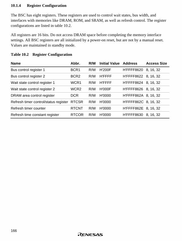
166
10.1.4 Register Configuration
The BSC has eight registers. These registers are used to control wait states, bus width, andinterfaces with memories like DRAM, ROM, and SRAM, as well as refresh control. The registerconfigurations are listed in table 10.2.
All registers are 16 bits. Do not access DRAM space before completing the memory interfacesettings. All BSC registers are all initialized by a power-on reset, but are not by a manual reset.Values are maintained in standby mode.
Table 10.2 Register Configuration
Name Abbr. R/W Initial Value Address Access Size
Bus control register 1 BCR1 R/W H'200F H'FFFF8620 8, 16, 32
Bus control register 2 BCR2 R/W H'FFFF H'FFFF8622 8, 16, 32
Wait state control register 1 WCR1 R/W H'FFFF H'FFFF8624 8, 16, 32
Wait state control register 2 WCR2 R/W H'000F H'FFFF8626 8, 16, 32
DRAM area control register DCR R/W H'0000 H'FFFF862A 8, 16, 32
Refresh timer control/status register RTCSR R/W H'0000 H'FFFF862C 8, 16, 32
Refresh timer counter RTCNT R/W H'0000 H'FFFF862E 8, 16, 32
Refresh time constant register RTCOR R/W H'0000 H'FFFF8630 8, 16, 32

167
10.1.5 Address Map
Figure 10.2 shows the address format used by the SH7040 Series.
A31–A24 A23, A22 A21
Output address:Output from the address pins
Space selection:Not output externally; used to select the type of spaceOn-chip ROM space or CS space when 00000000 (H'00)DRAM space when 00000001 (H'01)Reserved (do not access) when 00000010 to 11111110 (H'02 to H'FE)On-chip peripheral module space or on-chip RAM space when 11111111 (H'FF)
CS space selection:Decoded, outputs CS0 to CS3 when A31 to A24 = 00000000
A0
Figure 10.2 Address Format
This LSI uses 32-bit addresses:
• A31–A24 are used to select the type of space and are not output externally.
• Bits A23 and A22 are decoded and output as chip select signals (CS0–CS3) for thecorresponding areas when bits A31–A24 are 00000000.
• A21–A0 are output externally.
Table 10.3 shows an address map for on-chip ROM effective mode. Table 10.4 shows an addressmap for on-chip ROM ineffective mode.

168
Table 10.3 Address Map for On-Chip ROM Effective Mode
Address Space Memory Size Bus Width
H'00000000–H'0003FFFF* 1 On-chip ROM On-chip ROM memory 256 kbytes 32 bits
H'00040000–H'001FFFFF Reserved Reserved
H'00200000–H'003FFFFF CS0 space Ordinary space 2 Mbytes 8/16/32 bits* 2
H'00400000–H'007FFFFF CS1 space Ordinary space 4 Mbytes 8/16/32 bits* 2
H'00800000–H'00BFFFFF CS2 space Ordinary space 4 Mbytes 8/16/32 bits* 2
H'00C00000–H'00FFFFFF CS3 space Ordinary space ormultiplex I/O space
4 Mbytes 8/16/32 bits* 3
H'01000000–H'01FFFFFF DRAM space DRAM 16 Mbytes 8/16/32 bits* 2
H'02000000–H'FFFF7FFF Reserved Reserved
H'FFFF8000–H'FFFF87FF On-chipperipheralmodule
On-chip peripheralmodule
2 kbytes 8/16 bits
H'FFFF8800–H'FFFFEFFF Reserved Reserved
H'FFFFF000–H'FFFFFFFF On-chip RAM On-chip RAM 4 kbytes 32 bits
Notes: Do not access reserved spaces. Operation cannot be guaranteed if they are accessed.* 1 With the 64-kbyte version of on-chip ROM, the ROM address is H'0000000–
H'0000FFFF, and address H'00010000–H'0003FFFF is reserved space.With the 128-kbyte version of on-chip ROM, the ROM address is H'00000000–H'0001FFFF, and address H'00020000–H'0003FFFF is reserved space.
* 2 Selected by on-chip register settings.* 3 Ordinary space: selected by on-chip register settings.
Multiplex I/O space: 8/16 bit selected by the A14 bit.
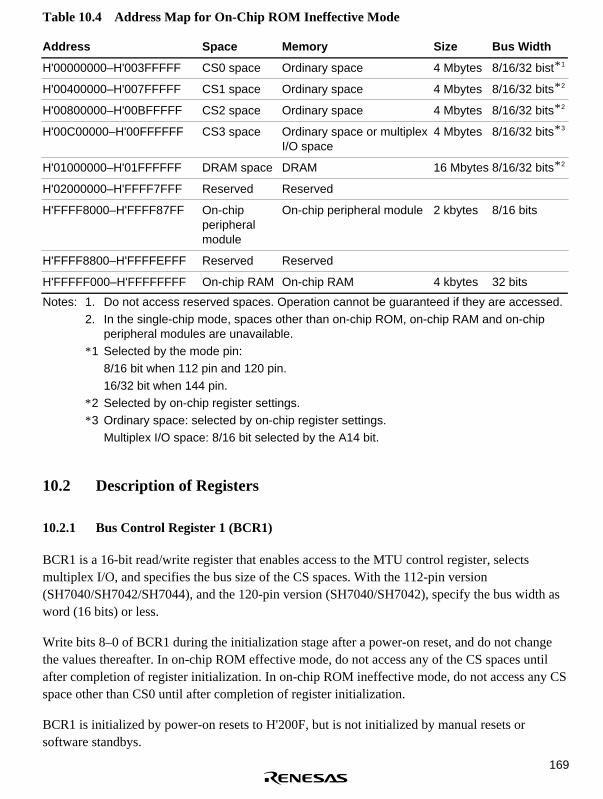
169
Table 10.4 Address Map for On-Chip ROM Ineffective Mode
Address Space Memory Size Bus Width
H'00000000–H'003FFFFF CS0 space Ordinary space 4 Mbytes 8/16/32 bist* 1
H'00400000–H'007FFFFF CS1 space Ordinary space 4 Mbytes 8/16/32 bits* 2
H'00800000–H'00BFFFFF CS2 space Ordinary space 4 Mbytes 8/16/32 bits* 2
H'00C00000–H'00FFFFFF CS3 space Ordinary space or multiplexI/O space
4 Mbytes 8/16/32 bits* 3
H'01000000–H'01FFFFFF DRAM space DRAM 16 Mbytes 8/16/32 bits* 2
H'02000000–H'FFFF7FFF Reserved Reserved
H'FFFF8000–H'FFFF87FF On-chipperipheralmodule
On-chip peripheral module 2 kbytes 8/16 bits
H'FFFF8800–H'FFFFEFFF Reserved Reserved
H'FFFFF000–H'FFFFFFFF On-chip RAM On-chip RAM 4 kbytes 32 bits
Notes: 1. Do not access reserved spaces. Operation cannot be guaranteed if they are accessed.2. In the single-chip mode, spaces other than on-chip ROM, on-chip RAM and on-chip
peripheral modules are unavailable.* 1 Selected by the mode pin:
8/16 bit when 112 pin and 120 pin.16/32 bit when 144 pin.
* 2 Selected by on-chip register settings.* 3 Ordinary space: selected by on-chip register settings.
Multiplex I/O space: 8/16 bit selected by the A14 bit.
10.2 Description of Registers
10.2.1 Bus Control Register 1 (BCR1)
BCR1 is a 16-bit read/write register that enables access to the MTU control register, selectsmultiplex I/O, and specifies the bus size of the CS spaces. With the 112-pin version(SH7040/SH7042/SH7044), and the 120-pin version (SH7040/SH7042), specify the bus width asword (16 bits) or less.
Write bits 8–0 of BCR1 during the initialization stage after a power-on reset, and do not changethe values thereafter. In on-chip ROM effective mode, do not access any of the CS spaces untilafter completion of register initialization. In on-chip ROM ineffective mode, do not access any CSspace other than CS0 until after completion of register initialization.
BCR1 is initialized by power-on resets to H'200F, but is not initialized by manual resets orsoftware standbys.

170
Bit: 15 14 13 12 11 10 9 8
— — MTURWE
— — — — IOE
Initial value: 0 0 1 0 0 0 0 0
R/W: R R R/W R R R R R/W
Bit: 7 6 5 4 3 2 1 0
A3LG A2LG A1LG A0LG A3SZ A2SZ A1SZ A0SZ
Initial value: 0 0 0 0 1 1 1 1
R/W: R/W R/W R/W R/W R/W R/W R/W R/W
• Bits 15, 14, 12–9—Reserved: These bits always read as 0. The write value should always be 0.
• Bit 13—MTU Read/Write Enable (MTURWE): When this bit is 1, MTU control registeraccess is enabled. See section 12, Multifunction Timer Pulse Unit (MTU), for details.
Bit 13 (MTURWE) Description
0 MTU control register access is disabled
1 MTU control register access is enabled (initial value)
• Bit 8—Multiplex I/O Enable (IOE): Selects the use of CS3 space as ordinary space oraddress/data multiplex I/O space. A 0 selects ordinary space and a 1 selects address/datamultiplex I/O space. When address/data multiplex I/O space is selected, the address and dataare multiplexed and output from the data bus. When CS3 space is an address/data multiplexI/O space, bus size is decided by the A14 bit (A14 = 0: 8 bit, A14 = 1: 16 bit).
Bit 8 (IOE) Description
0 CS3 space is ordinary space (initial value)
1 CS3 space is address/data multiplex I/O space
• Bit 7—CS3 Space Long Size Specification (A3LG): Specifies the CS3 space bus size. This iseffective only when CS3 space is ordinary space. When CS3 space is an address/data multiplexI/O space, bus size is decided by the A14 bit.
Bit 7 (A3LG) Description
0 According to the A3SZ bit specified value (initial value)
1 Longword (32 bit) size

171
• Bit 6—CS2 Space Long Size Specification (A2LG): Specifies the CS2 space bus size.
Bit 6 (A2LG) Description
0 According to the A2SZ bit value (initial value)
1 Longword (32 bit) size
• Bit 5—CS1 Space Long Size Specification (A1LG): Specifies the CS1 space bus size.
Bit 5 (A1LG) Description
0 According to the A1SZ bit value (initial value)
1 Longword (32 bit) size
• Bit 4—CS0 Space Long Size Specification (A0LG): Specifies the CS0 space bus size.
Bit 4 (A0LG) Description
0 According to the A0SZ bit value (initial value)
1 Longword (32 bit) size
Note: A0LG is effective only in on-chip ROM effective mode. When in on-chip ROM ineffectivemode, the CS0 space bus size is specified by the mode pin.
• Bit 3—CS3 Space Size Specification (A3SZ): Specifies the CS3 space bus size when A3LG =0. This is effective only when CS3 space is ordinary space. When CS3 space is an address/datamultiplex I/O space, bus size is decided by the A14 bit.
Bit 3 (A3SZ) Description
0 Byte (8 bit) size
1 Word (16 bit) size (initial value)
Note: This bit is ignored when A3LG = 1; CS3 space bus size becomes longword (32 bit) (forordinary space).
• Bit 2—CS2 Space Size Specification (A2SZ): Specifies the CS2 space bus size when A2LG =0.
Bit 2 (A2SZ) Description
0 Byte (8 bit) size
1 Word (16 bit) size (initial value)
Note: This bit is ignored when A2LG = 1; CS2 space bus size becomes longword (32 bit).

172
• Bit 1—CS1 Space Size Specification (A1SZ): Specifies the CS1 space bus size when A1LG =0.
Bit 1 (A1SZ) Description
0 Byte (8 bit) size
1 Word (16 bit) size (initial value)
Note: This bit is ignored when A1LG = 1; CS1 space bus size becomes longword (32 bit).
• Bit 0—CS0 Space Size Specification (A0SZ): Specifies the CS0 space bus size when A0LG =0.
Bit 0 (A0SZ) Description
0 Byte (8 bit) size
1 Word (16 bit) size (initial value)
Note: A0SZ is effective only in on-chip ROM effective mode. In on-chip ROM ineffective mode,the CS0 space bus size is specified by the mode pin. However, even in on-chip ROMeffective mode, this bit is ignored when A0LG = 1; CS0 space bus size becomes longword(32 bit).
10.2.2 Bus Control Register 2 (BCR2)
BCR2 is a 16-bit read/write register that specifies the number of idle cycles and CS signal assertextension of each CS space.
BCR2 is initialized by power-on resets to H'FFFF, but is not initialized by manual resets orsoftware standbys.
Bit: 15 14 13 12 11 10 9 8
IW31 IW30 IW21 IW20 IW11 IW10 IW01 IW00
Initial value: 1 1 1 1 1 1 1 1
R/W: R/W R/W R/W R/W R/W R/W R/W R/W
Bit: 7 6 5 4 3 2 1 0
CW3 CW2 CW1 CW0 SW3 SW2 SW1 SW0
Initial value: 1 1 1 1 1 1 1 1
R/W: R/W R/W R/W R/W R/W R/W R/W R/W

173
• Bits 15–8—Idles between Cycles (IW31, IW30, IW21, IW20, IW11, IW10, IW01, IW00):These bits specify idle cycles inserted between consecutive accesses when the second one is toa different CS area after a read. Idles are used to prevent data conflict between ROM (andother memories, which are slow to turn the read data buffer off), fast memories, and I/Ointerfaces. Even when access is to the same area, idle cycles must be inserted when a readaccess is followed immediately by a write access. The idle cycles to be inserted comply withthe area specification of the previous access. Refer to section 10.6, Waits between AccessCycles, for details.
IW31, IW30 specify the idle between cycles for CS3 space; IW21, IW20 specify the idlebetween cycles for CS2 space; IW11, IW10 specify the idle between cycles for CS1 space andIW01, IW00 specify the idle between cycles for CS0 space.
Bit 15 (IW31) Bit 14 (IW30) Description
0 0 No idle cycle after accessing CS3 space
1 Inserts one idle cycle after accessing CS3space
1 0 Inserts two idle cycles after accessing CS3space
1 Inserts three idle cycles after accessing CS3space (initial value)
Bit 13 (IW21) Bit 12 (IW20) Description
0 0 No idle cycle after accessing CS2 space
1 Inserts one idle cycle
1 0 Inserts two idle cycles
1 Inserts three idle cycles (initial value)
Bit 11 (IW11) Bit 10 (IW10) Description
0 0 No idle cycle after accessing CS1 space
1 Inserts one idle cycle
1 0 Inserts two idle cycles
1 Inserts three idle cycles (initial value)

174
Bit 9 (IW01) Bit 8 (IW00) Description
0 0 No idle cycle after accessing CS0 space
1 Inserts one idle cycle
1 0 Inserts two idle cycles
1 Inserts three idle cycles (initial value)
• Bits 7–4—Idle Specification for Continuous Access (CW3, CW2, CW1, CW0): Thecontinuous access idle specification makes insertions to clearly delineate the bus intervals byonce negating the CSn signal when doing consecutive accesses of the same CS space. When awrite immediately follows a read, the number of idle cycles inserted is the larger of the twovalues specified by IW and CW. Refer to section 10.6, Waits between Access Cycles, fordetails.
CW3 specifies the continuous access idles for CS3 space; CW2 specifies the continuous accessidles for CS2 space; CW1 specifies the continuous access idles for CS1 space and CW0specifies the continuous access idles for CS0 space.
Bit 7 (CW3) Description
0 No CS3 space continuous access idle cycles
1 One CS3 space continuous access idle cycle (initial value)
Bit 6 (CW2) Description
0 No CS2 space continuous access idle cycles
1 One CS2 space continuous access idle cycle (initial value)
Bit 5 (CW1) Description
0 No CS1 space continuous access idle cycles
1 One CS1 space continuous access idle cycle (initial value)
Bit 4 (CW0) Description
0 No CS0 space continuous access idle cycles
1 One CS0 space continuous access idle cycle (initial value)

175
• Bits 3–0—CS Assert Extension Specification (SW3, SW2, SW1, SW0): The CS assert cycleextension specification is for making insertions to prevent extension of the RD signal or WRxsignal assert period beyond the length of the CSn signal assert period. Extended cycles insertone cycle before and after each bus cycle, which simplifies interfaces with external devices andalso has the effect of extending write data hold time. Refer to section 10.3.3, CS Assert PeriodExtension, for details.
SW3 specifies the CS assert extension for CS3 space access; SW2 specifies the CS assertextension for CS2 space access; SW1 specifies the CS assert extension for CS1 space accessand SW0 specifies the CS assert extension for CS0 space access.
Bit 3 (SW3) Description
0 No CS3 space CS assert extension
1 CS3 space CS assert extension (initial value)
Bit 2 (SW2) Description
0 No CS2 space CS assert extension
1 CS2 space CS assert extension (initial value)
Bit 1 (SW1) Description
0 No CS1 space CS assert extension
1 CS1 space CS assert extension (initial value)
Bit 0 (SW0) Description
0 No CS0 space CS assert extension
1 CS0 space CS assert extension (initial value)
10.2.3 Wait Control Register 1 (WCR1)
WCR1 is a 16-bit read/write register that specifies the number of wait cycles (0–15) for each CSspace.
WCR1 is initialized by power-on resets to H'FFFF, but is not initialized by manual resets orsoftware standbys.

176
Bit: 15 14 13 12 11 10 9 8
W33 W32 W31 W30 W23 W22 W21 W20
Initial value: 1 1 1 1 1 1 1 1
R/W: R/W R/W R/W R/W R/W R/W R/W R/W
Bit: 7 6 5 4 3 2 1 0
W13 W12 W11 W10 W03 W02 W01 W00
Initial value: 1 1 1 1 1 1 1 1
R/W: R/W R/W R/W R/W R/W R/W R/W R/W
• Bits 15–12—CS3 Space Wait Specification (W33, W32, W31, W30): Specifies the number ofwaits for CS3 space access.
Bit 15(W33)
Bit 14(W32)
Bit 13(W31)
Bit 12(W30) Description
0 0 0 0 No wait (external wait input disabled)
0 0 0 1 1 wait external wait input enabled
⋅⋅⋅
1 1 1 1 15 wait external wait input enabled (initial value)
• Bits 11–8—CS2 Space Wait Specification (W23, W22, W21, W20): Specifies the number ofwaits for CS2 space access.
Bit 11(W23)
Bit 10(W22)
Bit 9(W21)
Bit 8(W20) Description
0 0 0 0 No wait (external wait input disabled)
0 0 0 1 1 wait external wait input enabled
⋅⋅⋅
1 1 1 1 15 wait external wait input enabled (initial value)

177
• Bits 7–4—CS1 Space Wait Specification (W13, W12, W11, W10): Specifies the number ofwaits for CS1 space access.
Bit 7(W13)
Bit 6(W12)
Bit 5(W11)
Bit 4(W10) Description
0 0 0 0 No wait (external wait input disabled)
0 0 0 1 1 wait external wait input enabled
⋅⋅⋅
1 1 1 1 15 wait external wait input enabled (initial value)
• Bits 3–0—CS0 Space Wait Specification (W03, W02, W01, W00): Specifies the number ofwaits for CS0 space access.
Bit 3(W03)
Bit 2(W02)
Bit 1(W01)
Bit 0(W00) Description
0 0 0 0 No wait (external wait input disabled)
0 0 0 1 1 wait external wait input enabled
⋅⋅⋅
1 1 1 1 15 wait external wait input enabled (initial value)
10.2.4 Wait Control Register 2 (WCR2)
WCR2 is a 16-bit read/write register that specifies the number of access cycles for DRAM spaceand CS space for DMA single address mode transfers.
Do not perform any DMA single address transfers before WCR2 is set.
WCR2 is initialized by power-on resets to H'000F, but is not initialized by manual resets orsoftware standbys.
Bit: 15 14 13 12 11 10 9 8
— — — — — — — —
Initial value: 0 0 0 0 0 0 0 0
R/W: R R R R R R R R
Bit: 7 6 5 4 3 2 1 0
— — DDW1 DDW0 DSW3 DSW2 DSW1 DSW0
Initial value: 0 0 0 0 1 1 1 1
R/W: R R R/W R/W R/W R/W R/W R/W

178
• Bits 15–6—Reserved: These bits always read as 0. The write value should always be 0.
• Bits 5–4—DRAM Space DMA Single Address Mode Access Wait Specification (DDW1,DDW0): Specifies the number of waits for DRAM space access during DMA single addressmode accesses. These bits are independent of the DWW and DWR bits of the DCR.
Bit 5 (DDW1) Bit 4 (DDW0) Description
0 0 2-cycle (no wait) external wait disabled(initial value)
1 3-cycle (1 wait) external wait disabled
1 0 4-cycle (2 wait) external wait enabled
1 5-cycle (3 wait) external wait enabled
• Bits 3–0—CS Space DMA Single Address Mode Access Wait Specification (DSW3, DSW2,DSW1, DSW0): Specifies the number of waits for CS space access (0–15) during DMA singleaddress mode accesses. These bits are independent of the W bits of the WCR1.
Bit 3(DSW3)
Bit 2(DSW2)
Bit 1(DSW1)
Bit 0(DSW0) Description
0 0 0 0 No wait (external wait input disabled)
0 0 0 1 1 wait (external wait input enabled)
⋅⋅⋅
1 1 1 1 15 wait (external wait input enabled) (initial value)
10.2.5 DRAM Area Control Register (DCR)
DCR is a 16-bit read/write register that selects the number of waits, operation mode, number ofaddress multiplex shifts and the like for DRAM control.
Do not perform any DRAM space accesses before DCR initial settings are completed.
DCR is initialized by power-on resets to H'0000, but is not initialized by manual resets or softwarestandbys.

179
Bit: 15 14 13 12 11 10 9 8
TPC RCD TRAS1 TRAS0 DWW1 DWW0 DWR1 DWR0
Initial value: 0 0 0 0 0 0 0 0
R/W: R/W R/W R/W R/W R/W R/W R/W R/W
Bit: 7 6 5 4 3 2 1 0
DIW — BE RASD SZ1 SZ0 AMX1 AMX0
Initial value: 0 0 0 0 0 0 0 0
R/W: R/W R R/W R/W R/W R/W R/W R/W
• Bit 15—RAS Precharge Cycle Count (TPC): Specifies the minimum number of cycles afterRAS is negated before next assert.
Bit 15 (TPC) Description
0 1.5 cycles (initial value)
1 2.5 cycles
• Bit 14—RAS-CAS Delay Cycle Count (RCD): Specifies the number of row address outputcycles.
Bit 14 (RCD) Description
0 1 cycle (initial value)
1 2 cycles
• Bits 13–12—CAS-Before-RAS Refresh RAS Assert Cycle Count (TRAS1–TRAS0): Specifythe number of RAS assert cycles for CAS before RAS refreshes.
Bit 13 (TRAS1) Bit 12 (TRAS0) Description
0 0 2.5 cycles (initial value)
1 3.5 cycles
1 0 4.5 cycles
1 5.5 cycles

180
• Bits 11–10—DRAM Write Cycle Wait Count (DWW1–DWW0): Specifies the number ofDRAM write cycle column address output cycles.
Bit 11 (DWW1) Bit 10 (DWW0) Description
0 0 2-cycle (no wait) external wait disabled (initial value)
1 3-cycle (1 wait) external wait disabled
1 0 4-cycle (2 wait) external wait enabled
1 5-cycle (3 wait) external wait enabled
• Bits 9–8—DRAM Read Cycle Wait Count (DWR1–DWR0): Specifies the number of DRAMread cycle column address output cycles.
Bit 9 (DWR1) Bit 8 (DWR0) Description
0 0 2-cycle (no wait) external wait disabled (initial value)
1 3-cycle (1 wait) external wait disabled
1 0 4-cycle (2 wait) external wait enabled
1 5-cycle (3 wait) external wait enabled
• Bit 7—DRAM Idle Cycle Count (DIW): Specifies whether to insert idle cycles, either whenaccessing a different external space (CS space) or when doing a DRAM write, after DRAMreads.
Bit 7 (DIW) Description
0 No idle cycles (initial value)
1 1 idle cycle
• Bit 6—Reserved: This bit always reads as 0. The write value should always be 0.
• Bit 5—Burst Enable (BE): Specifies the DRAM operation mode.
Bit 5 (BE) Description
0 Burst disabled (initial value)
1 DRAM high-speed page mode enabled.
• Bit 4—RAS Down Mode (RASD): Specifies the DRAM operation mode.
Bit 4 (RASD) Description
0 Access DRAM by RAS up mode (initial value)
1 Access DRAM by RAS down mode

181
• Bits 3–2—DRAM Bus Width Specification (SZ1, SZ0): Specifies the DRAM space bus width.
Bit 3 (SZ1) Bit 2 (SZ0) Description
0 0 Byte (8 bits) (initial value)
1 Word (16 bits)
1 Don’t care Longword (32 bits)
• Bits 1–0—DRAM Address Multiplex (AMX1–AMX0): Specifies the DRAM addressmultiplex count.
Bit 1 (AMX1) Bit 0 (AMX0) Description
0 0 9 bit (initial value)
1 10 bit
1 0 11 bit
1 12 bit
10.2.6 Refresh Timer Control/Status Register (RTCSR)
RTCSR is a 16-bit read/write register that selects the refresh mode and the clock input to therefresh timer counter (RTCNT), and controls compare match interrupts (CMI).
RTCSR is initialized by power-on resets and hardware standbys to H'0000, but is not initialized bymanual resets or software standbys.
Bit: 15 14 13 12 11 10 9 8
— — — — — — — —
Initial value: 0 0 0 0 0 0 0 0
R/W: R R R R R R R R
Bit: 7 6 5 4 3 2 1 0
— CMF CMIE CKS2 CKS1 CKS0 RFSH RMD
Initial value: 0 0 0 0 0 0 0 0
R/W: R R/W R/W R/W R/W R/W R/W R/W
• Bits 15–7—Reserved: These bits always read as 0. The write value should always be 0.

182
• Bit 6—Compare Match Flag (CMF): This status flag, which indicates that the values ofRTCNT and RTCOR match, is set/cleared under the following conditions:
Bit 6 (CMF) Description
0 Clear condition: After RTCSR is read when CMF is 1, 0 is written inCMF. In some cases it will clear when DTC is activated by a comparematch interrupt; refer to section 8, Data Transfer Controller (DTC), fordetails. (initial value)
1 Set condition: RTCNT = RTCOR. When both RTCNT and RTCOR arein an initialized state (when values have not been rewritten sinceinitialization, and RTCNT has not had its value changed due to a count-up), RTCNT and RTCOR match, as both are H'0000, but in this caseCMF is not set.
• Bit 5—Compare Match Interrupt Enable (CMIE): Enables or disables an interrupt requestcaused by the CMF bit of the RTCSR when CMF is set to 1.
Bit 5 (CMIE) Description
0 Disables an interrupt request caused by CMF (initial value)
1 Enables an interrupt request caused by CMF
• Bits 4–2—Clock Select (CKS2–CKS0): Select the clock to input to RTCNT from among theseven types of internal clock obtained from dividing the system clock (φ).
Bit 4 (CKS2) Bit 3 (CKS1) Bit 2 (CKS0) Description
0 0 0 Stops count-up (initial value)
1 φ/2
1 0 φ/8
1 φ/32
1 0 0 φ/128
1 φ/512
1 0 φ/2048
1 φ/4096
• Bit 1—Refresh Control (RFSH): Selects whether to use refresh control for DRAM.
Bit 1 (RFSH) Description
0 Do not refresh DRAM (initial value)
1 Refresh DRAM

183
• Bit 0—Refresh Mode (RMD): When the RFSH bit is 1, this bit selects normal refresh or self-refresh. When the RFSH bit is 1, self-refresh mode is entered immediately after the RMD bit isset to 1. When RMD is cleared to 0, a CAS-before-RAS refresh is performed at the interval setin the refresh time constant register (RTCNT).
When set for self-refresh, the SH7040 Series enters self-refresh mode immediately unless it isin the middle of a DRAM access. If it is, it enters self-refresh mode when the access ends.Refresh requests from the interval timer are ignored in self-refresh mode.
Bit 0 (RMD) Description
0 CAS-before-RAS refresh (initial value)
1 Self-refresh
10.2.7 Refresh Timer Counter (RTCNT)
RTCNT is a 16-bit read/write register that is used as an 8-bit up counter for refreshes or generatinginterrupt requests.
RTCNT counts up with the clock selected by the CKS2–CKS0 bits of the RTCSR. RTCNT valuescan always be read/written by the CPU. When RTCNT matches RTCOR, RTCNT is cleared toH'0000 and the CMF flag of the RTCSR is set to 1. If the RFSH bit of RTCSR is 1 and the RMDbit is 0 at this time, a CAS-before-RAS refresh is performed. Additionally, if the CMIE bit ofRTCSR is a 1, a compare match interrupt (CMI) is generated.
Bits 15–8 are reserved and play no part in counter operation. They are always read as 0.
RTCNT is initialized by power-on resets H'0000, but is not initialized by manual resets orsoftware standbys.
Bit: 15 14 13 12 11 10 9 8
— — — — — — — —
Initial value: 0 0 0 0 0 0 0 0
R/W: R R R R R R R R
Bit: 7 6 5 4 3 2 1 0
Initial value: 0 0 0 0 0 0 0 0
R/W: R/W R/W R/W R/W R/W R/W R/W R/W

184
10.2.8 Refresh Time Constant Register (RTCOR)
RTCOR is a 16-bit read/write register that establishes the compare match period with RTCNT.The values of RTCOR and RTCNT are constantly compared. When the values correspond, thecompare match flag of RTCSR is set and RTCNT is cleared to 0.
When the refresh bit (RFSH) of the RTCSR is set to 1 and the RMD bit is 0, a refresh requestsignal is produced by this match. The refresh request signal is held until a refresh operation isperformed. If the refresh request is not processed before the next match, the previous requestbecomes ineffective.
When the CMIE bit of the RTSCR is set to 1, an interrupt request is sent to the interrupt controllerby this match signal. The interrupt request is output continuously until the CMF bit of the RTSCRis cleared.
Bits 15–8 are reserved and cannot be used in setting the period. They always read 0.
RTCOR is initialized by power-on resets to H'0000, but is not initialized by manual resets orsoftware standbys.
Bit: 15 14 13 12 11 10 9 8
— — — — — — — —
Initial value: 0 0 0 0 0 0 0 0
R/W: R R R R R R R R
Bit: 7 6 5 4 3 2 1 0
Initial value: 0 0 0 0 0 0 0 0
R/W: R/W R/W R/W R/W R/W R/W R/W R/W
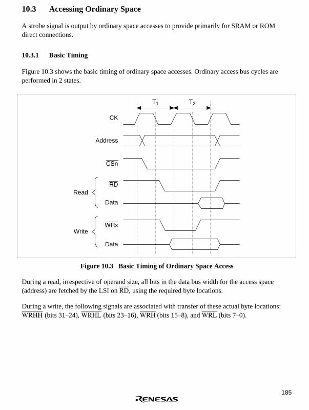
185
10.3 Accessing Ordinary Space
A strobe signal is output by ordinary space accesses to provide primarily for SRAM or ROMdirect connections.
10.3.1 Basic Timing
Figure 10.3 shows the basic timing of ordinary space accesses. Ordinary access bus cycles areperformed in 2 states.
T1
CK
Address
CSn
RDRead
Write
Data
WRx
Data
T2
Figure 10.3 Basic Timing of Ordinary Space Access
During a read, irrespective of operand size, all bits in the data bus width for the access space(address) are fetched by the LSI on RD, using the required byte locations.
During a write, the following signals are associated with transfer of these actual byte locations:WRHH (bits 31–24), WRHL (bits 23–16), WRH (bits 15–8), and WRL (bits 7–0).

186
10.3.2 Wait State Control
The number of wait states inserted into ordinary space access states can be controlled using theWCR settings (figure 10.4).
T1 TW
CK
Read
Write
Address
CSn
RD
Data
WRx
Data
T2
Figure 10.4 Wait Timing of Ordinary Space Access (Software Wait Only)

187
When the wait is specified by software using WCR, the wait input WAIT signal from outside issampled. Figure 10.5 shows the WAIT signal sampling. The WAIT signal is sampled at the clockrise one cycle before the clock rise when Tw state shifts to T2 state.
T1 TW
CK
Read
Write
Address
CSn
WAIT
RD
Data
WRx
Data
TW TW0 T2
Figure 10.5 Wait State Timing of Ordinary Space Access (Wait States from Software Wait2 State + WAIT Signal)
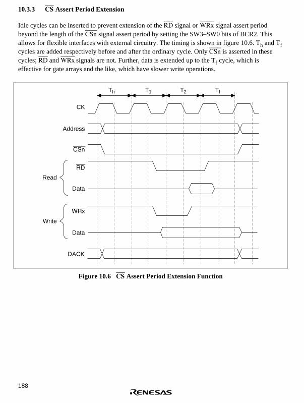
188
10.3.3 CS Assert Period Extension
Idle cycles can be inserted to prevent extension of the RD signal or WRx signal assert periodbeyond the length of the CSn signal assert period by setting the SW3–SW0 bits of BCR2. Thisallows for flexible interfaces with external circuitry. The timing is shown in figure 10.6. Th and Tfcycles are added respectively before and after the ordinary cycle. Only CSn is asserted in thesecycles; RD and WRx signals are not. Further, data is extended up to the Tf cycle, which iseffective for gate arrays and the like, which have slower write operations.
Th T1
CK
Read
Write
Address
CSn
RD
Data
WRx
Data
T2 Tf
DACK
Figure 10.6 CS Assert Period Extension Function

189
10.4 DRAM Access
10.4.1 DRAM Direct Connection
When address space A31–A24 = H'01 has been accessed, the corresponding space becomes a 16-Mbyte DRAM space, and the DRAM interface function can be used to directly connect theSH7040 Series to DRAM.
Row address and column address are always multiplexed for DRAM space. The amount of rowaddress multiplexing can be selected as from 9 to 12 bits by setting the AMX1 and AMX0 bits ofthe DCR.
Table 10.5 AMX Bits and Address Multiplex Output
Row Address Column Address
AMX1 AMX0ShiftAmount
Output Pins OutputAddress
OutputAddress
OutputPins
0 0 9 bit A21–A15 A21–A15 A21–A0 A21–A0
A14–A0 A23–A9
0 1 10 bit A21–A14 A21–A14 A21–A0 A21–A0
A13–A0 A23–A10
1 0 11 bit A21–A13 A21–A13 A21–A0 A21–A0
A12–A0 A23–A11
1 1 12 bit A21–A12 A21–A12 A21–A0 A21–A0
A11–A0 A23–A12
In addition to ordinary read and write accesses, burst mode access using high speed page mode issupported.
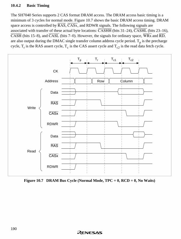
190
10.4.2 Basic Timing
The SH7040 Series supports 2 CAS format DRAM access. The DRAM access basic timing is aminimum of 3 cycles for normal mode. Figure 10.7 shows the basic DRAM access timing. DRAMspace access is controlled by RAS, CASx, and RDWR signals. The following signals areassociated with transfer of these actual byte locations: CASHH (bits 31–24), CASHL (bits 23–16),CASH (bits 15–8), and CASL (bits 7–0). However, the signals for ordinary space, WRx and RD,are also output during the DMAC single transfer column address cycle period. Tp is the prechargecycle, Tr is the RAS assert cycle, Tc is the CAS assert cycle and Tc2 is the read data fetch cycle.
Tp Tr Tc1 Tc2
CK
Write
Read
Address
Data
RAS
CASx
RDWR
Data
RDWR
CASx
RAS
Row Column
Figure 10.7 DRAM Bus Cycle (Normal Mode, TPC = 0, RCD = 0, No Waits)

191
10.4.3 Wait State Control
Wait state insertion during DRAM space access is controlled by setting the TPC, RCD, DWW1,DWW0, DWR1, and DWR0 bits of the DCR. TPC and RCD are common to both reads andwrites. The timing with waits inserted is shown in figures 10.8 through 10.11. External waits canbe inserted at the time of software waits 2, 3. The sampling location is the same as that of ordinaryspace: at one cycle before the Tc2 cycle clock rise. Wait cycles are extended by external waits.
Tp Tr Tc1 Tcw1 Tc2
CK
Write
Read
Address
Data
RAS
CASx
RDWR
Data
RDWR
CASx
RAS
Row Column
Figure 10.8 DRAM Bus Cycle (Normal Mode, TPC = 0, RCD = 0, One Wait)

192
Tp Tr Trw Tc1 Tcw1 Tcw2 Tcw2Tpw
CK
Write
Read
Address
Data
RAS
CASx
RDWR
Data
RDWR
CASx
RAS
Row Column
Figure 10.9 DRAM Bus Cycle (Normal Mode, TPC = 1, RCD = 1, Two Waits)

193
Tp Tc1 Tcw1 Tcw2 Tcw3 Tc2Tr
CK
Write
Read
Address
Data
RAS
CASx
RDWR
Data
RDWR
CASx
RAS
Row Column
Figure 10.10 DRAM Bus Cycle (Normal Mode, TPC = 0, RCD = 0, Three Waits)
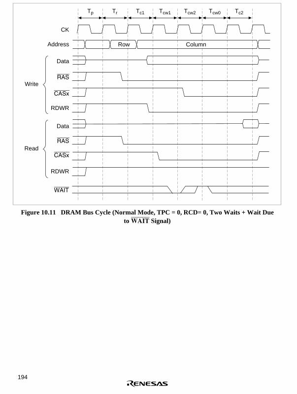
194
Tp Tc1 Tcw1 Tcw2 Tcw0 Tc2Tr
CK
Write
Read
Address
Data
RAS
CASx
RDWR
Data
RDWR
CASx
RAS
Row Column
WAIT
Figure 10.11 DRAM Bus Cycle (Normal Mode, TPC = 0, RCD= 0, Two Waits + Wait Dueto WAIT Signal)

195
10.4.4 Burst Operation
High-Speed Page Mode: When the burst enable bit (BE) of the DCR is set, burst accesses can beperformed using high speed page mode. The timing is shown in figure 10.12. Wait cycles can beinserted during burst accesses by using the DCR.
Tp Tc1 Tc2 Tc1 Tc2Tr
CK
Write
Read
Address
Data
RAS
CASx
RDWR
Data
RDWR
CASx
RAS
Row Column Column
Figure 10.12 DRAM Bus Cycle (High-Speed Page Mode)
RAS Down Mode: There are some instances where even if burst operation is selected, continuousaccesses to DRAM will not occur, but another space will be accessed instead part way through theaccess. In such cases, if the RAS signal is maintained at low level during the time the other spaceis accessed, it is possible to continue burst operation at the time the next DRAM same row addressis accessed. This is called RAS down mode.
To use RAS down mode, set both the BE and RASD bits of the DCR to 1.
Figures 10.13 and 10.14 show operation in RAS up and down modes.

196
CK
RAS
CASx
DRAM access DRAM accessCS space
access
Address
Data
CS space
Tp Tr Tc1 Tc2 T1 T2 Tp Tr Tc1 Tc2
Column ColumnRow Row
Figure 10.13 DRAM Access Normal Operation (RAS Up Mode)
CK
RAS
CASx
DRAM accessDRAM access
CS space access
Address
Data
Row Column CS space
Tp Tr Tc1 Tc2 T1 T2 Tc1 Tc2
Column
Figure 10.14 RAS Down Mode

197
10.4.5 Refresh Timing
The bus state controller is equipped with a function to control refreshes of DRAM. CAS-before-RAS (CBR) refresh or self-refresh can be selected by setting the RTCSR’s RMD bit.
CAS-before-RAS Refresh: For CBR refreshes, set the RCR’s RMD bit to 0 and the RFSH bit to1. Also write the values in RTCNT and RTCOR necessary to fulfill the refresh interval prescribedfor the DRAM being used. When a clock is selected with the CKS2–CKS0 bits of the RSTCR,RTCNT starts counting up from the value at that time. The RTCNT value is constantly comparedto the RTCOR value and a CBR refresh is performed when the two match. RTCNT is cleared atthat time and the count starts again. Figure 10.15 shows the timing for the CBR refresh operation.
The number of RAS assert cycles in the refresh cycle is set by the TRAS1, TRAS0 bits of theDCR.
CK
CASx
RAS
TRp TRr1 TRr2 TRc TRc
Figure 10.15 CAS-Before-RAS Refresh Timing (TRAS1, TRAS0 = 0, 0)

198
Self-Refresh: When both the RMD and RFSH bits of the RTCSR are set to 1, the CAS signal andRAS signal are output and the DRAM enters self-refresh mode, as shown in figure 10.16. Do notaccess DRAM during self-refreshes, in order to preserve DRAM data. When performing DRAMaccesses, first cancel the self-refresh, then access only after doing individual refreshes for all rowaddresses within the time prescribed for the particular DRAM.
For external bus right requests during self-refreshes, to preserve DRAM data at the time ofreleasing the bus rights, only CASx, RAS, and RDWR are output and the bus rights are released tothe external device with the self-refresh maintained. Consequently, do not perform DRAMaccesses from external devices at such a time.
CK
CASx
RAS
TRp TRr1 TRr2 TRc TRc
Figure 10.16 Self-Refresh Timing

199
10.5 Address/Data Multiplex I/O Space Access
When the BCR1 register IOE bit is set to 1, the D15–D0 pins can be used for multiplexedaddress/data I/O for the CS3 space. Consequently, peripheral LSIs requiring address/datamultiplexing can be directly connected to this LSI.
Address/data multiplex I/O space bus width is selected by the A14 bit, and is 8 bit when A14 = 0and 16 bit when A14 = 1.
10.5.1 Basic Timing
When the IOE bit of the BCR1 is set to 1, CS3 space becomes address/data multiplex I/O space.When this space is accessed, addresses and data are multiplexed. When the A14 address bit is 0,the bus size becomes 8 bit and addresses and data are input and output through the D7–D0 pins.When the A14 address bit is 1, the bus size becomes 16 bit and address output and data I/O occurthrough the D15–D0 pins. Access for the address/data multiplex I/O space is controlled by theAH, RD, and WRx signals.
Address/data multiplex I/O space accesses are done after a 3-cycle (fixed) address output, as anordinary space type access (figure 10.17).
CK
CS3
AH
RD
Data
WRx
Data
Address
Ta1 Ta2 Ta3 Ta4 T1 T2
Read
Write
Address output
Address output Data output
Data input
Figure 10.17 Address/Data Multiplex I/O Space Access Timing (No Waits)

200
10.5.2 Wait State Control
Setting the WCR controls waits during address/data multiplex I/O space accesses. Software waitand external wait insertion timing is the same as during ordinary space accesses. The timing forone software wait + one external wait inserted is shown in figure 10.18.
CK
CS3
AH
RD
Data
WRx
Data
WAIT
Address
Ta1 Ta2 Ta3 Ta4 T1 TW TWo T2
Read
Write
Address output
Address output Data output
Data input
Figure 10.18 Address/Data Multiplex I/O Space Access Wait State Timing (One SoftwareWait + One External Wait)

201
10.5.3 CS Assertion Extension
The timing diagram when setting CS assertion extension during address/data multiplex I/O spaceaccess is shown in figure 10.19.
CS3
AH
RD
Data
WRxx
Data
Address
Ta1 Ta2 Ta3 Ta4 Th T1 T2 Tf
Read
Write
Address output
Address output Data output
Data input
Figure 10.19 Wait Timing in Address/Data Multiplex I/O Space when CS AssertionExtension is Set
10.6 Waits between Access Cycles
When a read from a slow device is completed, data buffers may not go off in time to prevent dataconflicts with the next access. If there is a data conflict during memory access, the problem can besolved by inserting a wait in the access cycle.
To enable detection of bus cycle starts, waits can be inserted between access cycles duringcontinuous accesses of the same CS space by negating the CSn signal once.
10.6.1 Prevention of Data Bus Conflicts
For the two cases of write cycles after read cycles, and read cycles for a different area after readcycles, waits are inserted so that the number of idle cycles specified by the IW31–IW00 bits of the

202
BCR2 and the DIW of the DCR occur. When idle cycles already exist between access cycles, onlythe number of empty cycles remaining beyond the specified number of idle cycles are inserted.
Figure 10.20 shows an example of idles between cycles. In this example, 1 idle between CSnspace cycles has been specified, so when a CSm space write immediately follows a CSn spaceread cycle, 1 idle cycle is inserted.
CK
CSn
CSm
RD
Data
CSn space read CSm space writeIdle cycle
WRx
Address
T1 T2 T1 T2Tidle
Figure 10.20 Idle Cycle Insertion Example
IW31 and IW30 specify the number of idle cycles required after a CS3 space read either to readother external spaces, or for this LSI, to do write accesses. In the same manner, IW21 and IW20specify the number of idle cycles after a CS2 space read, IW11 and IW10, the number after a CS1space read, and IW01 and IW00, the number after a CS0 space read.
DIW specifies the number of idle cycles required, after a DRAM space read either to read otherexternal spaces (CS space), or for this LSI, to do write accesses.
0 to 3 cycles can be specified for CS space, and 0 to 1 cycle for DRAM space.
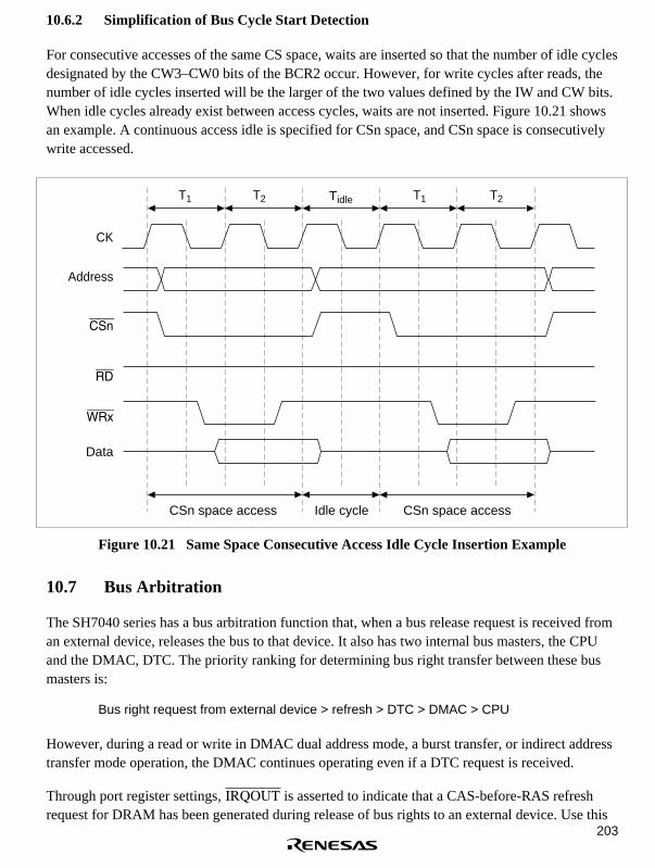
203
10.6.2 Simplification of Bus Cycle Start Detection
For consecutive accesses of the same CS space, waits are inserted so that the number of idle cyclesdesignated by the CW3–CW0 bits of the BCR2 occur. However, for write cycles after reads, thenumber of idle cycles inserted will be the larger of the two values defined by the IW and CW bits.When idle cycles already exist between access cycles, waits are not inserted. Figure 10.21 showsan example. A continuous access idle is specified for CSn space, and CSn space is consecutivelywrite accessed.
CK
CSn
RD
WRx
Data
CSn space access CSn space accessIdle cycle
Address
T1 T2 T1 T2Tidle
Figure 10.21 Same Space Consecutive Access Idle Cycle Insertion Example
10.7 Bus Arbitration
The SH7040 series has a bus arbitration function that, when a bus release request is received froman external device, releases the bus to that device. It also has two internal bus masters, the CPUand the DMAC, DTC. The priority ranking for determining bus right transfer between these busmasters is:
Bus right request from external device > refresh > DTC > DMAC > CPU
However, during a read or write in DMAC dual address mode, a burst transfer, or indirect addresstransfer mode operation, the DMAC continues operating even if a DTC request is received.
Through port register settings, IRQOUT is asserted to indicate that a CAS-before-RAS refreshrequest for DRAM has been generated during release of bus rights to an external device. Use this

204
to cause the external device to negate the BREQ and return the bus rights to the SH7040 Series.Please note that if the external device does not return the bus rights within the time prescribed forthe DRAM refresh interval, this LSI will not be able to perform the refresh operation and theDRAM contents cannot be guaranteed.
Figure 10.22 shows the bus right release procedure.
BREQ = Low
SH704X
BREQ accepted
Strobe pin:high-level output
Address, data,strobe pin:
high impedance
Bus right releaseresponse
Bus right release status
External device
Bus right request
BACK confirmation
Bus right acquisition
BACK = Low
Figure 10.22 Bus Right Release Procedure

205
10.8 Memory Connection Examples
Figures 10.23–10.31 show examples of the memory connections.
As A21–A18 become input ports in power-on reset, they should be handled (e.g. pulled down) as necessary.
SH704x32k × 8 bits
CE
OE
CSn
RD
A0–A14
D0–D7
A0–A14
I/O0–I/O7
ROM
Figure 10.23 8-Bit Data Bus Width ROM Connection
SH704x256k × 16 bits
ROM
CE
OE
CSn
RD
A0
A1–A18
D0–D15
A0–A17
I/O0–I/O15
Figure 10.24 16-Bit Data Bus Width ROM Connection

206
SH704x
CSn
RD
CE
CE
OE
OEA0
A1
A2–A19
D16–D31
D0–D15
A0–A17
A0–A17
I/O0–I/O15
I/O0–I/O15
256k × 16 bitsROM
Figure 10.25 32-Bit Data Bus Width ROM Connection
SH704x
CSn
RD
WRL WE
CS
OE
A0–A16 A0–A16
D0–D7 I/O0–I/O7
123k × 8 bitsSRAM
Figure 10.26 8-Bit Data Bus Width SRAM Connection

207
SH704x128k × 8 bits
SRAM
CSnRD
CSOE
A0A1–A17 A0–A16
WRH WED8–D15 I/O0–I/O7
WRLD0–D7
CS
OE
A0–A16
WE
I/O0–I/O7
Figure 10.27 16-Bit Data Bus Width SRAM Connection

208
SH704x
CSCSnRD OEA0A1
A2–A18 A0–A16
WRHH WED24–D31 I/O0–I/O7
WRHLD16–D23
D0–D7
WRL
WRHD8–D15
CS
OE
A0–A16
WE
I/O0–I/O7
CS
OE
A0–A16
WE
I/O0–I/O7
I/O0–I/O7
CS
OEA0–A16
WE
128k × 8 bitsSRAM
Figure 10.28 32-Bit Data Bus Width SRAM Connection

209
SH704x
RAS
RDWR
A0–A9
CASLAD0–AD7
RAS
WE
A0–A9
CASI/O0–I/O7
OE
512k × 8 bitsDRAM
Figure 10.29 8-Bit Data Bus Width DRAM Connection
RAS RAS
RDWR WE
A0OE
A1–A9
CASH UCAS
CASL LCAS
AD0–AD15 I/O0–I/O15
SH704x256k × 16 bits
DRAM
A0–A8
Figure 10.30 16-Bit Data Bus Width DRAM Connection

210
SH704x256k × 16 bits
DRAM
RAS
RDWR
A0
A1
A2–A10
CASHHCASHL
AD16–AD31
RAS
WE
OE
A0–A8
UCASLCASI/O0–I/O15
I/O0–I/O15
CASH
CASLAD0–AD15
RAS
WEOE
A0–A8
UCASLCAS
Figure 10.31 32-Bit Data Bus Width DRAM Connection
10.9 On-Chip Peripheral I/O Register Access
On-chip peripheral I/O registers are accessed from the bus state controller, as shown in table 10.6.
Table 10.6 On-Chip Peripheral I/O Register Access
On-chipPeripheral Module SCI
MTU,POE INTC
PFC,PORT CMT A/D* UBC WDT DMAC DTC CACHE
Connected buswidth
8bit 16bit 16bit 16bit 16bit 16bit 16bit 16bit 16bit 16bit 16bit
Access cycle 2cyc 2cyc 2cyc 2cyc 2cyc 2cyc 3cyc 3cyc 3cyc 3cyc 3cyc
Note: * A/D of A mask products are accessed in 8-bit width, 3 cyc.

211
Cycles in which Bus is not Released
(a) One bus cycle:
The bus is never released during a single bus cycle. For example, in the case of a longword read(or write) in 8-bit normal space, the four memory accesses to the 8-bit normal space constitute asingle bus cycle, and the bus is never released during this period. Assuming that one memoryaccess requires two states, the bus is not released during an 8-state period.
8 bit 8 bit 8 bit 8 bit
Cycles in whichBus is not Released
Figure 10.32 One Bus Cycle
10.10 CPU Operation when Program is in External Memory
In the SH7040 Series, two words (equivalent to two instructions) are normally fetched in a singleinstruction fetch. This is also true when the program is located in external memory, irrespective ofwhether the external memory bus width is 8 or 16 bits.
If the program counter value immediately after the program branches is an odd-word (2n + 1)address, or if the program counter value immediately before the program branches is an even-word(2n) address, the CPU will always fetch 32 bits (equivalent to two instructions) that include therespective word instruction.

212

213
Section 11 Direct Memory Access Controller (DMAC)
11.1 Overview
The SH7040 Series includes an on-chip four-channel direct memory access controller (DMAC).The DMAC can be used in place of the CPU to perform high-speed data transfers among externaldevices equipped with DACK (transfer request acknowledge signal), external memories, memory-mapped external devices, and on-chip peripheral modules (except for the DMAC, DTC, BSC, andUBC). Using the DMAC reduces the burden on the CPU and increases operating efficiency of theLSI as a whole.
11.1.1 Features
The DMAC has the following features:
• Four channels
• Four Gbytes of address space in the architecture
• Byte, word, or longword selectable data transfer unit
• 16 Mbytes (16,777,216 transfers, maximum)
• Single or dual address mode. Dual address mode can be direct or indirect address transfer.
Single address mode: Either the transfer source or transfer destination (peripheral device) isaccessed by a DACK signal while the other is accessed by address. One transfer unit ofdata is transferred in each bus cycle.
Dual address mode: Both the transfer source and transfer destination are accessed byaddress. Dual address mode can be direct or indirect address transfer.
• Direct access: Values set in a DMAC internal register indicate the accessed address forboth the transfer source and transfer destination. Two bus cycles are required for onedata transfer.
• Indirect access: The value stored at the location pointed to by the address set in theDMAC internal transfer source register is used as the address. Operation is otherwisethe same as direct access. This function can only be set for channel 3. Four bus cyclesare required for one data transfer.
• Channel function: Transfer modes that can be set are different for each channel. (Dual addressmode indirect access can only be set for channel 1. Only direct access is possible for the otherchannels.)
Channel 0: Single or dual address mode. External requests are accepted.
Channel 1: Single or dual address mode. External requests are accepted.
Channel 2: Dual address mode only. Source address reload function operates every fourthtransfer.

214
Channel 3: Dual address mode only. Direct address transfer mode and indirect addresstransfer mode selectable.
• Reload function: Enables automatic reloading of the value set in the first source addressregister every fourth DMA transfer. This function can be executed on channel 2 only.
• Transfer requests: There are three DMAC transfer activation requests, as indicated below.
External request: From two DREQ pins. DREQ can be detected either by falling edge or bylow level. External requests can only be received on channels 0 or 1.
Requests from on-chip peripheral modules: Transfer requests from on-chip modules such asSCI or A/D. These can be received by all channels.
Auto-request: The transfer request is generated automatically within the DMAC.
• Selectable bus modes: Cycle-steal mode or burst mode
• Two types of DMAC channel priority ranking:
Fixed priority mode: Always fixed
Round robin mode: Sets the lowest priority level for the channel that received the executionrequest last
• CPU can be interrupted when the specified number of data transfers are complete.
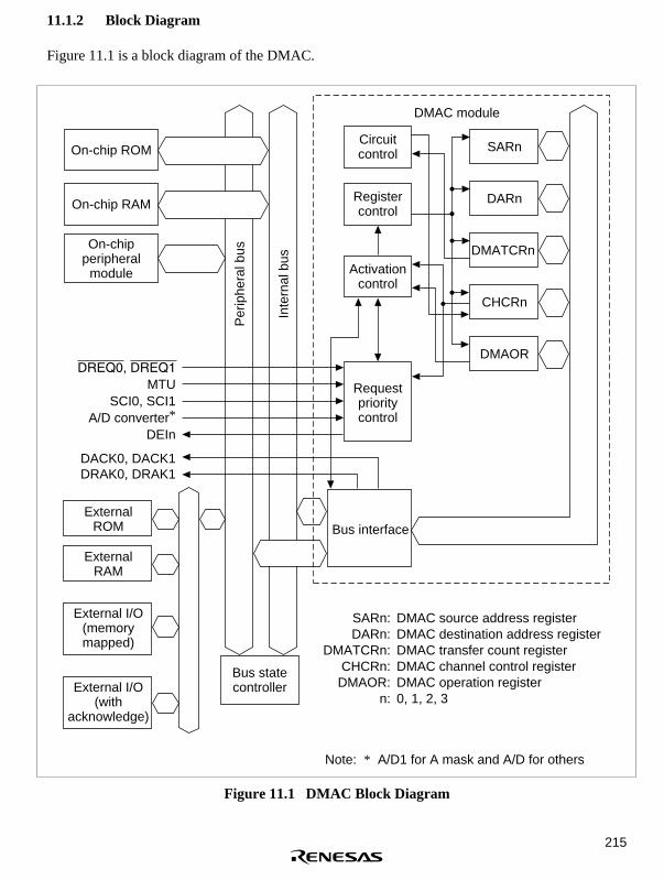
215
11.1.2 Block Diagram
Figure 11.1 is a block diagram of the DMAC.
On-chip ROM
Per
iphe
ral b
us
Inte
rnal
bus
On-chip RAM
DREQ0, DREQ1
Circuitcontrol SARn
DMAC module
Registercontrol
Activationcontrol
Requestprioritycontrol
Bus interface
Bus statecontroller
On-chipperipheral
module
DARn
DMATCRn
CHCRn
DMAOR
MTUSCI0, SCI1
A/D converter*
DEIn
ExternalROM
ExternalRAM
External I/O(memorymapped)
External I/O(with
acknowledge)
DACK0, DACK1DRAK0, DRAK1
SARn:DARn:
DMATCRn:CHCRn:
DMAOR:n:
DMAC source address registerDMAC destination address registerDMAC transfer count registerDMAC channel control registerDMAC operation register0, 1, 2, 3
Note: * A/D1 for A mask and A/D for others
Figure 11.1 DMAC Block Diagram

216
11.1.3 Pin Configuration
Table 11.1 shows the DMAC pins.
Table 11.1 DMAC Pin Configuration
Channel Name Symbol I/O Function
0 DMA transfer request DREQ0 I DMA transfer request input fromexternal device to channel 0
DMA transfer requestacknowledge
DACK0 O DMA transfer strobe output fromchannel 0 to external device
DREQ0 acceptanceconfirmation
DRAK0 O Sampling receive acknowledge outputfor DMA transfer request input fromexternal source
1 DMA transfer request DREQ1 I DMA transfer request input fromexternal device to channel 1
DMA transfer requestacknowledge
DACK1 O DMA transfer strobe output fromchannel 1 to external device
DREQ1 acceptanceconfirmation
DRAK1 O Sampling receive acknowledge outputfor DMA transfer request input fromexternal source

217
11.1.4 Register Configuration
Table 11.2 summarizes the DMAC registers. DMAC has a total of 17 registers. Each channel hasfour control registers. One other control register is shared by all channels
Table 11.2 DMAC Registers
Chan-nel Name
Abbrevi-ation R/W
InitialValue Address
RegisterSize
AccessSize
0 DMA source addressregister 0
SAR0 R/W Undefined H'FFFF86C0 32 bit 16, 32* 2
DMA destinationaddress register 0
DAR0 R/W Undefined H'FFFF86C4 32 bit 16, 32* 2
DMA transfer countregister 0
DMATCR0 R/W Undefined H'FFFF86C8 32 bit 16, 32* 3
DMA channel controlregister 0
CHCR0 R/W* 1 H'00000000 H'FFFF86CC 32 bit 16, 32* 2
1 DMA source addressregister 1
SAR1 R/W Undefined H'FFFF86D0 32 bit 16, 32* 2
DMA destinationaddress register 1
DAR1 R/W Undefined H'FFFF86D4 32 bit 16, 32* 2
DMA transfer countregister 1
DMATCR1 R/W Undefined H'FFFF86D8 32 bit 16, 32* 3
DMA channel controlregister 1
CHCR1 R/W* 1 H'00000000 H'FFFF86DC 32 bit 16, 32* 2
2 DMA source addressregister 2
SAR2 R/W Undefined H'FFFF86E0 32 bit 16, 32* 2
DMA destinationaddress register 2
DAR2 R/W Undefined H'FFFF86E4 32 bit 16, 32* 2

218
Table 11.2 DMAC Registers (cont)
Chan-nel Name
Abbrevi-ation R/W
InitialValue Address
RegisterSize
AccessSize
2(cont)
DMA transfer countregister 2
DMATCR2 R/W Undefined H'FFFF86E8 32 bit 16, 32* 3
DMA channel controlregister 2
CHCR2 R/W* 1 H'00000000 H'FFFF86EC 32 bit 16, 32* 2
3 DMA source addressregister 3
SAR3 R/W Undefined H'FFFF86F0 32 bit 16, 32* 2
DMA destinationaddress register 3
DAR3 R/W Undefined H'FFFF86F4 32 bit 16, 32* 2
DMA transfer countregister 3
DMATCR3 R/W Undefined H'FFFF86F8 32 bit 16, 32* 3
DMA channel controlregister 3
CHCR3 R/W* 1 H'00000000 H'FFFF86FC 32 bit 16, 32* 2
SharedDMA operationregister
DMAOR R/W* 1 H'0000 H'FFFF86B0 16 bit 16, 32* 4
Notes: Do not attempt to access an empty address. If an access is attemped, the systemoperation is not guarenteed.* 1 Write 0 after reading 1 in bit 1 of CHCR0–CHCR3 and in bits 1 and 2 of the DMAOR to
clear flags. No other writes are allowed.* 2 For 16-bit access of SAR0–SAR3, DAR0–DAR3, and CHCR0–CHCR3, the 16-bit value
on the side not accessed is held.* 3 DMATCR has a 24-bit configuration: bits 0–23. Writing to the upper 8 bits (bits 24–31)
is invalid, and these bits always read 0.* 4 Do not make 32-bit access for DMAOR.
11.2 Register Descriptions
11.2.1 DMA Source Address Registers 0–3 (SAR0–SAR3)
DMA source address registers 0–3 (SAR0–SAR3) are 32-bit read/write registers that specify thesource address of a DMA transfer. These registers have a count function, and during a DMAtransfer, they indicate the next source address. In single-address mode, SAR values are ignoredwhen a device with DACK has been specified as the transfer source.
Specify a 16-bit or 32-bit boundary address when doing 16-bit or 32-bit data transfers. Operationcannot be guaranteed on any other addresses.
The initial value after power-on resets or in software standby mode is undefined. These registersare not initialized with manual reset.

219
Bit: 31 30 29 28 27 26 25 24
Initial value: — — — — — — — —
R/W: R/W R/W R/W R/W R/W R/W R/W R/W
Bit: 23 22 21 … … 2 1 0
… …
Initial value: — — — … … — — —
R/W: R/W R/W R/W … … R/W R/W R/W
11.2.2 DMA Destination Address Registers 0–3 (DAR0–DAR3)
DMA destination address registers 0–3 (DAR0–DAR3) are 32-bit read/write registers that specifythe destination address of a DMA transfer. These registers have a count function, and during aDMA transfer, they indicate the next destination address. In single-address mode, DAR values areignored when a device with DACK has been specified as the transfer destination.
Specify a 16-bit or 32-bit boundary address when doing 16-bit or 32-bit data transfers. Operationcannot be guaranteed on any other address. The initial value after power-on resets or in softwarestandby mode, is undefined. These registers are not initialized with manual reset.
Bit: 31 30 29 28 27 26 25 24
Initial value: — — — — — — — —
R/W: R/W R/W R/W R/W R/W R/W R/W R/W
Bit: 23 22 21 … … 2 1 0
… …
Initial value: — — — … … — — —
R/W: R/W R/W R/W … … R/W R/W R/W
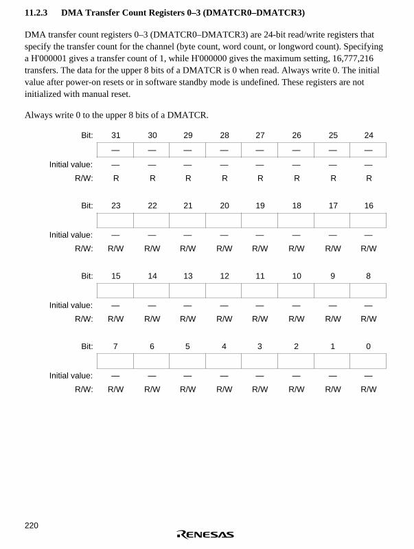
220
11.2.3 DMA Transfer Count Registers 0–3 (DMATCR0–DMATCR3)
DMA transfer count registers 0–3 (DMATCR0–DMATCR3) are 24-bit read/write registers thatspecify the transfer count for the channel (byte count, word count, or longword count). Specifyinga H'000001 gives a transfer count of 1, while H'000000 gives the maximum setting, 16,777,216transfers. The data for the upper 8 bits of a DMATCR is 0 when read. Always write 0. The initialvalue after power-on resets or in software standby mode is undefined. These registers are notinitialized with manual reset.
Always write 0 to the upper 8 bits of a DMATCR.
Bit: 31 30 29 28 27 26 25 24
— — — — — — — —
Initial value: — — — — — — — —
R/W: R R R R R R R R
Bit: 23 22 21 20 19 18 17 16
Initial value: — — — — — — — —
R/W: R/W R/W R/W R/W R/W R/W R/W R/W
Bit: 15 14 13 12 11 10 9 8
Initial value: — — — — — — — —
R/W: R/W R/W R/W R/W R/W R/W R/W R/W
Bit: 7 6 5 4 3 2 1 0
Initial value: — — — — — — — —
R/W: R/W R/W R/W R/W R/W R/W R/W R/W

221
11.2.4 DMA Channel Control Registers 0–3 (CHCR0–CHCR3)
DMA channel control registers 0–3 (CHCR0–CHCR3) is a 32-bit read/write register where theoperation and transmission of each channel is designated. They are initialized by a power-on resetand in software standby mode. There is no initializing with manual reset.
Bit: 31 30 29 28 27 26 25 24
— — — — — — — —
Initial value: — — — — — — — —
R/W: R R R R R R R R
Bit: 23 22 21 20 19 18 17 16
— — — DI* 2 RO* 2 RL* 2 AM* 2 AL* 2
Initial value: — — — 0 0 0 0 0
R R R (R/W) (R/W) (R/W) (R/W) (R/W)
Bit: 15 14 13 12 11 10 9 8
DM1 DM0 SM1 SM0 RS3 RS2 RS1 RS0
Initial value: 0 0 0 0 0 0 0 0
R/W: R/W R/W R/W R/W R/W R/W R/W R/W
Bit: 7 6 5 4 3 2 1 0
— DS* 2 TM TS1 TS0 IE TE DE
Initial value: — 0 0 0 0 0 0 0
R/W: R (R/W) R/W R/W R/W R/W R/(W) * 1 R/W
Notes: * 1 TE bit: Allows only 0 write after reading 1.* 2 The DI, RO, RL, AM, AL, or DS bit may be absent, depending on the channel.
• Bits 31–21—Reserved bits: Data are 0 when read. The write value always be 0.
• Bit 20—Direct/Indirect (DI): Specifies either direct address mode operation or indirect addressmode operation for channel 3 source address. This bit is valid only in CHCR3. It always reads0 for CHCR0–CHCR2, and cannot be modified.
Bit 20: DI Description
0 Direct access mode operation for channel 3 (initial value)
1 Indirect access mode operation for channel 3

222
• Bit 19—Source Address Reload (RO): Selects whether to reload the source address initialvalue during channel 2 transfer. This bit is valid only for channel 2. It always reads 0 forCHCR0, CHCR1, and CHCR3, and cannot be modified.
Bit 19: RO Description
0 Does not reload source address (initial value)
1 Reloads source address
• Bit 18—Request Check Level (RL): Selects whether to output DRAK notifying externaldevice of DREQ received, with active high or active low. This bit is valid only for CHCR0 andCHCR1. It always reads 0 for CHCR2 and CHCR3, and cannot be modified.
Bit 18: RL Description
0 Output DRAK with active high (initial value)
1 Output DRAK with active low
• Bit 17—Acknowledge Mode (AM): In dual address mode, selects whether to output DACK inthe data write cycle or data read cycle. In single address mode, DACK is always outputirrespective of the setting of this bit. This bit is valid only for CHCR0 and CHCR1. It alwaysreads as 0 for CHCR2 and CHCR3, and cannot be modified.
Bit 17: AM Description
0 Outputs DACK during read cycle (initial value)
1 Outputs DACK during write cycle
• Bit 16—Acknowledge Level (AL): Specifies whether to set DACK (acknowledge) signaloutput to active high or active low. This bit is valid only with CHCR0 and CHCR1. It alwaysreads as 0 for CHCR2 and CHCR3, and cannot be modified.
Bit 16: AL Description
0 Active high output (initial value)
1 Active low output

223
• Bits 15 and 14—Destination Address Mode 1, 0 (DM1 and DM0): These bits specifyincrement/decrement of the DMA transfer destination address. These bit specifications areignored when transferring data from an external device to address space in single addressmode.
Bit 15: DM1 Bit 14: DM0 Description
0 0 Destination address fixed (initial value)
0 1 Destination address incremented (+1 during 8-bit transfer, +2during 16-bit transfer, +4 during 32-bit transfer)
1 0 Destination address decremented (–1 during 8-bit transfer, –2during 16-bit transfer, –4 during 32-bit transfer)
1 1 Setting prohibited
• Bits 13 and 12—Source Address Mode 1, 0 (SM1 and SM0): These bits specifyincrement/decrement of the DMA transfer source address. These bit specifications are ignoredwhen transferring data from an external device to address space in single address mode.
Bit 13: SM1 Bit 12: SM0 Description
0 0 Source address fixed (initial value)
0 1 Source address incremented (+1 during 8-bit transfer, +2during 16-bit transfer, +4 during 32-bit transfer)
1 0 Source address decremented (–1 during 8-bit transfer, –2during 16-bit transfer, –4 during 32-bit transfer)
1 1 Setting prohibited
When the transfer source is specified at an indirect address, specify in source address register 3(SAR3) the actual storage address of the data you want to transfer as the data storage address(indirect address).
During indirect address mode, SAR3 obeys the SM1/SM0 setting for increment/decrement. In thiscase, SAR3’s increment/decrement is fixed at +4/–4 or 0, irrespective of the transfer data sizespecified by TS1 and TS0.

224
• Bits 11–8—Resource Select 3–0 (RS3–RS0): These bits specify the transfer request source.
Bit 11:RS3
Bit 10:RS2
Bit 9:RS1
Bit 8:RS0 Description
0 0 0 0 External request, dual address mode (initial value)
0 0 0 1 Prohibited
0 0 1 0 External request, single address mode. External addressspace → external device.
0 0 1 1 External request, single address mode. External device →external address space.
0 1 0 0 Auto-request
0 1 0 1 Prohibited
0 1 1 0 MTU TGI0A
0 1 1 1 MTU TGI1A
1 0 0 0 MTU TGI2A
1 0 0 1 MTU TGI3A
1 0 1 0 MTU TGI4A
1 0 1 1 A/D ADI*
1 1 0 0 SCI0 TXI0
1 1 0 1 SCI0 RXI0
1 1 1 0 SCI1 TXI1
1 1 1 1 SCI1 RXI1
Notes: External request designations are valid only for channels 0 and 1. No transfer requestsources can be set for channels 2 or 3.* ADI1 for A mask.
• Bit 7—Reserved bits: Data is 0 when read. The write value always be 0.
• Bit 6—DREQ Select (DS): Sets the sampling method for the DREQ pin in external requestmode to either low-level detection or falling-edge detection. This bit is valid only with CHCR0and CHCR1. For CHCR2 and CHCR3, this bit always reads as 0 and cannot be modified.
Even with channels 0 and 1, when specifying an on-chip peripheral module or auto-request asthe transfer request source, this bit setting is ignored. The sampling method is fixed at falling-edge detection in cases other than auto-request.
Bit 6: DS Description
0 Low-level detection (initial value)
1 Falling-edge detection

225
• Bit 5—Transfer Mode (TM): Specifies the bus mode for data transfer.
Bit 5: TM Description
0 Cycle steal mode (initial value)
1 Burst mode
• Bits 4 and 3—Transfer Size 1, 0 (TS1, TS0): Specifies size of data for transfer.
Bit 4: TS1 Bit 3: TS0 Description
0 0 Specifies byte size (8 bits) (initial value)
0 1 Specifies word size (16 bits)
1 0 Specifies longword size (32 bits)
1 1 Prohibited
• Bit 2—Interrupt Enable (IE): When this bit is set to 1, interrupt requests are generated after thenumber of data transfers specified in the DMATCR (when TE = 1).
Bit 2: IE Description
0 Interrupt request not generated after DMATCR-specified transfer count(initial value)
1 Interrupt request enabled on completion of DMATCR specified numberof transfers
• Bit 1—Transfer End Flag (TE): This bit is set to 1 after the number of data transfers specifiedby the DMATCR. At this time, if the IE bit is set to 1, an interrupt request is generated.
If data transfer ends before TE is set to 1 (for example, due to an NMI or address error, orclearing of the DE bit or DME bit of the DMAOR) the TE is not set to 1. With this bit set to 1,data transfer is disabled even if the DE bit is set to 1.
Bit 1: TE Description
0 DMATCR-specified transfer count not ended (initial value)
Clear condition: 0 write after TE = 1 read, Power-on reset, standbymode
1 DMATCR specified number of transfers completed
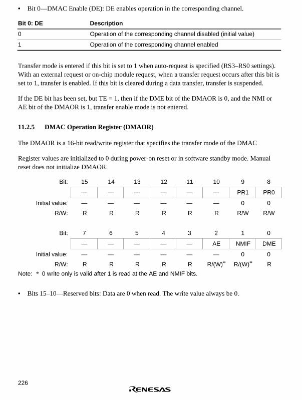
226
• Bit 0—DMAC Enable (DE): DE enables operation in the corresponding channel.
Bit 0: DE Description
0 Operation of the corresponding channel disabled (initial value)
1 Operation of the corresponding channel enabled
Transfer mode is entered if this bit is set to 1 when auto-request is specified (RS3–RS0 settings).With an external request or on-chip module request, when a transfer request occurs after this bit isset to 1, transfer is enabled. If this bit is cleared during a data transfer, transfer is suspended.
If the DE bit has been set, but TE = 1, then if the DME bit of the DMAOR is 0, and the NMI orAE bit of the DMAOR is 1, transfer enable mode is not entered.
11.2.5 DMAC Operation Register (DMAOR)
The DMAOR is a 16-bit read/write register that specifies the transfer mode of the DMAC
Register values are initialized to 0 during power-on reset or in software standby mode. Manualreset does not initialize DMAOR.
Bit: 15 14 13 12 11 10 9 8
— — — — — — PR1 PR0
Initial value: — — — — — — 0 0
R/W: R R R R R R R/W R/W
Bit: 7 6 5 4 3 2 1 0
— — — — — AE NMIF DME
Initial value: — — — — — — 0 0
R/W: R R R R R R/(W)* R/(W)* R
Note: * 0 write only is valid after 1 is read at the AE and NMIF bits.
• Bits 15–10—Reserved bits: Data are 0 when read. The write value always be 0.

227
• Bits 9–8—Priority Mode 1 and 0 (PR1 and PR0): These bits determine the priority level ofchannels for execution when transfer requests are made for several channels simultaneously.
Bit 9: PR1 Bit 8: PR0 Description
0 0 CH0 > CH1 > CH2 > CH3 (initial value)
0 1 CH0 > CH2 > CH3 > CH1
1 0 CH2 > CH0 > CH1 > CH3
1 1 Round robin mode
• Bits 7–3—Reserved bits: Data are 0 when read. The write value always be 0.
• Bit 2—Address Error Flag (AE): Indicates that an address error has occurred during DMAtransfer. If this bit is set during a data transfer, transfers on all channels are suspended. TheCPU cannot write a 1 to the AE bit. Clearing is effected by 0 write after 1 read.
Bit 2: AE Description
0 No address error, DMA transfer enabled (initial value)
Clearing condition: Write AE = 0 after reading AE = 1
1 Address error, DMA transfer disabled
Setting condition: Address error due to DMAC
• Bit 1—NMI Flag (NMIF): Indicates input of an NMI. This bit is set irrespective of whether theDMAC is operating or suspended. If this bit is set during a data transfer, transfers on allchannels are suspended. The CPU is unable to write a 1 to the NMIF. Clearing is effected by a0 write after 1 read.
Bit 1: NMIF Description
0 No NMI interrupt, DMA transfer enabled (initial value)
Clearing condition: Write NMIF = 0 after reading NMIF = 1
1 NMI has occurred, DMC transfer prohibited
Set condition: NMI interrupt occurrence

228
• Bit 0—DMAC Master Enable (DME): This bit enables activation of the entire DMAC. Whenthe DME bit and DE bit of the CHCR for the corresponding channel are set to 1, that channelis transfer-enabled. If this bit is cleared during a data transfer, transfers on all channels aresuspended.
Even when the DME bit is set, when the TE bit of the CHCR is 1, or its DE bit is 0, transfer isdisabled in the case of an NMI of the DMAOR or when AE = 1.
Bit 0: DME Description
0 Disable operation on all channels (initial value)
1 Enable operation on all channels
11.3 Operation
When there is a DMA transfer request, the DMAC starts the transfer according to thepredetermined channel priority order; when the transfer end conditions are satisfied, it ends thetransfer. Transfers can be requested in three modes: auto-request, external request, and on-chipperipheral module request. Transfer can be in either the single address mode or the dual addressmode, and dual address mode can be either direct or indirect address transfer mode. The bus modecan be either burst or cycle steal.
11.3.1 DMA Transfer Flow
After the DMA source address registers (SAR), DMA destination address registers (DAR), DMAtransfer count register (DMATCR), DMA channel control registers (CHCR), and DMA operationregister (DMAOR) are set to the desired transfer conditions, the DMAC transfers data accordingto the following procedure:
1. The DMAC checks to see if transfer is enabled (DE = 1, DME = 1, TE = 0, NMIF = 0,AE = 0).
2. When a transfer request comes and transfer has been enabled, the DMAC transfers 1 transferunit of data (determined by TS0 and TS1 setting). For an auto-request, the transfer beginsautomatically when the DE bit and DME bit are set to 1. The DMATCR value will bedecremented by 1 upon each transfer. The actual transfer flows vary by address mode and busmode.
3. When the specified number of transfers have been completed (when DMATCR reaches 0), thetransfer ends normally. If the IE bit of the CHCR is set to 1 at this time, a DEI interrupt is sentto the CPU.
4. When an address error occurs in the DMAC or an NMI interrupt is generated, the transfer isaborted. Transfers are also aborted when the DE bit of the CHCR or the DME bit of theDMAOR are changed to 0.

229
Figure 11.2 is a flowchart of this procedure.
Normal end
DoesNMIF = 1, AE = 1,DE = 0, or DME
= 0?
Bus mode,transfer request mode,
DREQ detection selectionsystem
Initial settings(SAR, DAR, TCR, CHCR, DMAOR)
Transfer (1 transfer unit);DMATCR – 1 → DMATCR, SAR, and DAR
updated
DEI interrupt request (when IE = 1)
No
Yes
No
Yes
No
Yes
Yes
No
Yes
No
*3
*2
Start
Transfer aborted
Notes: *1*2*3
In auto-request mode, transfer begins when NMIF, AE, and TE are all 0,and the DE and DME bits are set to 1.DREQ = level detection in burst mode (external request), or cycle-stealmode.DREQ = edge detection in burst mode (external request), or auto-request mode in burst mode.
DMATCR = 0?
Transfer requestoccurs?*1
DE, DME = 1 andNMIF, AE, TE = 0?
DoesNMIF = 1, AE = 1,DE = 0, or DME
= 0?
Transfer ends
Figure 11.2 DMAC Transfer Flowchart

230
11.3.2 DMA Transfer Requests
DMA transfer requests are usually generated in either the data transfer source or destination, butthey can also be generated by devices and on-chip peripheral modules that are neither the sourcenor the destination. Transfers can be requested in three modes: auto-request, external request, andon-chip peripheral module request. The request mode is selected in the RS3–RS0 bits of the DMAchannel control registers 0–3 (CHCR0–CHCR3).
Auto-Request Mode: When there is no transfer request signal from an external source, as in amemory-to-memory transfer or a transfer between memory and an on-chip peripheral moduleunable to request a transfer, the auto-request mode allows the DMAC to automatically generate atransfer request signal internally. When the DE bits of CHCR0–CHCR3 and the DME bit of theDMAOR are set to 1, the transfer begins (so long as the TE bits of CHCR0–CHCR3 and theNMIF and AE bits of DMAOR are all 0).
External Request Mode: In this mode a transfer is performed at the request signal (DREQ) of anexternal device. Choose one of the modes shown in table 11.3 according to the application system.When this mode is selected, if the DMA transfer is enabled (DE = 1, DME = 1, TE = 0, NMIF = 0,AE = 0), a transfer is performed upon a request at the DREQ input. Choose to detect DREQ byeither the falling edge or low level of the signal input with the DS bit of CHCR0–CHCR3 (DS = 0is level detection, DS = 1 is edge detection). The source of the transfer request does not have to bethe data transfer source or destination.
Table 11.3 Selecting External Request Modes with the RS Bits
RS3 RS2 RS1 RS0 Address Mode Source Destination
0 0 0 0 Dual addressmode
Any* Any*
0 0 1 0 Single addressmode
External memory ormemory-mappedexternal device
External device withDACK
0 0 1 1 Single addressmode
External device withDACK
External memory ormemory-mappedexternal device
Note: * External memory, memory-mapped external device, on-chip memory, on-chip peripheralmodule (excluding DMAC, DTC, BSC, UBC).
On-Chip Peripheral Module Request Mode: In this mode a transfer is performed at the transferrequest signal (interrupt request signal) of an on-chip peripheral module. As indicated in table11.4, there are ten transfer request signals: five from the multifunction timer pulse unit (MTU),which are compare match or input capture interrupts; the receive data full interrupts (RxI) andtransmit data empty interrupts (TxI) of the two serial communication interfaces (SCI); and the A/Dconversion end interrupt (ADI1 for A mask, ADI for others) of the A/D converter. When DMA

231
transfers are enabled (DE = 1, DME = 1, TE = 0, NMIF = 0, AE = 0), a transfer is performed uponthe input of a transfer request signal.
The transfer request source need not be the data transfer source or transfer destination. However,when the transfer request is set by RxI (transfer request because SCI’s receive data is full), thetransfer source must be the SCI’s receive data register (RDR). When the transfer request is set byTxI (transfer request because SCI’s transmit data is empty), the transfer destination must be theSCI’s transmit data register (TDR). Also, if the transfer request is set to the A/D converter, thedata transfer destination must be the A/D converter register.
Table 11.4 Selecting On-Chip Peripheral Module Request Modes with the RS Bits
RS3 RS2 RS1 RS0DMAC TransferRequest Source
DMA TransferRequest SignalSource
Destin-ation Bus Mode
0 1 1 0 MTU* 2 TGI0A Any* 1 Any* 1 Burst/cycle steal
0 1 1 1 MTU* 2 TGI1A Any* 1 Any* 1 Burst/cycle steal
1 0 0 0 MTU* 2 TGI2A Any* 1 Any* 1 Burst/cycle steal
1 0 0 1 MTU* 2 TGI3A Any* 1 Any* 1 Burst/cycle steal
1 0 1 0 MTU* 2 TGI4A Any* 1 Any* 1 Burst/cycle steal
1 0 1 1 A/D ADI* 5 ADDR* 4 Any* 1 Burst/cycle steal
1 1 0 0 SCI0* 3 transmit block TxI0 Any* 1 TDR0 Burst/cycle steal
1 1 0 1 SCI0* 3 transmit block RxI0 RDR0 Any* 1 Burst/cycle steal
1 1 1 0 SCI1* 3 transmit block TxI1 Any* 1 TDR1 Burst/cycle steal
1 1 1 1 SCI1* 3 transmit block RxI1 RDR1 Any* 1 Burst/cycle steal
Notes: * 1 External memory, memory-mapped external device, on-chip memory, on-chipperipheral module (excluding DMAC, DTC, BSC, UBC).
* 2 MTU: Multifunction timer pulse unit.* 3 SCI0, SCI1: Serial communications interface.* 4 ADDR0, ADDR1: A/D converter’s A/D register.* 5 ADI1 for A mask.
In order to output a transfer request from an on-chip peripheral module, set the relevant interruptenable bit for each module, and output an interrupt signal.
When an on-chip peripheral module’s interrupt request signal is used as a DMA transfer requestsignal, interrupts for the CPU are not generated.
When a DMA transfer is conducted corresponding with one of the transfer request signals in table11.4, it is automatically discontinued. In cycle steal mode this occurs in the first transfer, and inburst mode with the last transfer.
232
11.3.3 Channel Priority
When the DMAC receives simultaneous transfer requests on two or more channels, it selects achannel according to a predetermined priority order, either in a fixed mode or in round robinmode. These modes are selected by priority bits PR1 and PR0 in the DMA operation register(DMAOR).
Fixed Mode: In these modes, the priority levels among the channels remain fixed.
The following priority orders are available for fixed mode:
• CH0 > CH1 > CH2 > CH3
• CH0 > CH2 > CH3 > CH1
• CH2 > CH0 > CH1 > CH3
These are selected by settings of the PR1 and PR0 bits of the DMA operation register (DMAOR).
Round Robin Mode: In round robin mode, each time the transfer of one transfer unit (byte, wordor long word) ends on a given channel, that channel receives the lowest priority level (figure 11.3).The priority level in round robin mode immediately after a reset is CH0 > CH1 > CH2 > CH3.

233
CH1 > CH2 > CH3 > CH0
CH0 > CH1 > CH2 > CH3
CH2 > CH3 > CH0 > CH1
CH0 > CH1 > CH2 > CH3
CH2 > CH3 > CH0 > CH1
CH0 > CH1 > CH2 > CH3
CH0 > CH1 > CH2 > CH3
CH3 > CH0 > CH1 > CH2
CH0 > CH1 > CH2 > CH3
Transfer on channel 0
Initial priority setting
Initial priority setting
Initial priority setting
Initial priority setting No change in priority.
When channel 2 receives thelowest priority, the prioritiesof channel 0 and 1, whichwere above channel 2, are also shifted simultaneously. Immedi-ately thereafter, if there is a transfer request for channel 1 only, channel1 is given the lowest priority,and the priorities of channels 3and 0 are simultaneouslyshifted down.
When channel 1 is given the lowest priority, the priorityof channel 0, which was above channel 1, is also shifted simultaneously.
Channel 0 is given the lowestpriority.
Priority after transfer
Priority after transfer
Priority after transfer
Priority after transfer
Priority after transferdue to issue of a transferrequest for channel 1only.
Transfer on channel 1
Transfer on channel 2
Transfer on channel 3
Figure 11.3 Round Robin Mode

234
Figure 11.4 shows the changes in priority levels when transfer requests are issued simultaneouslyfor channels 0 and 3, and channel 1 receives a transfer request during a transfer on channel 0. TheDMAC operates in the following manner under these circumstances:
1. Transfer requests are issued simultaneously for channels 0 and 3.
2. Since channel 0 has a higher priority level than channel 3, the channel 0 transfer is conductedfirst (channel 3 is on transfer standby).
3. A transfer request is issued for channel 1 during a transfer on channel 0 (channels 1 and 3 areon transfer standby).
4. At the end of the channel 0 transfer, channel 0 shifts to the lowest priority level.
5. At this point, channel 1 has a higher priority level than channel 3, so the channel 1 transfercomes first (channel 3 is on transfer standby).
6. When the channel 1 transfer ends, channel 1 shifts to the lowest priority level.
7. Channel 3 transfer begins.
8. When the channel 3 transfer ends, channel 3 and channel 2 priority levels are lowered, givingchannel 3 the lowest priority.
Transfer request Channel waiting DMAC operation Channel priority
Issued for channels 0 and 3Issued for channel 1
0 > 1 > 2 > 3Channel 0 transfer begins
1 > 2 > 3 > 0Channel 0transfer endsChannel 1transfer begins
Channel 3transfer begins
2 > 3 > 0 > 1Channel 1 transfer ends
0 > 1 > 2 > 3Channel 3transfer ends
Change of priority
Change of priority
Change of priority
None
3
3
1,3
Figure 11.4 Example of Changes in Priority in Round Robin Mode

235
11.3.4 DMA Transfer Types
The DMAC supports the transfers shown in table 11.5. It can operate in the single address mode,in which either the transfer source or destination is accessed using an acknowledge signal, or dualaccess mode, in which both the transfer source and destination addresses are output. The dualaccess mode consists of a direct address mode, in which the output address value is the object of adirect data transfer, and an indirect address mode, in which the output address value is not theobject of the data transfer, but the value stored at the output address becomes the transfer objectaddress. The actual transfer operation timing varies with the bus mode. The DMAC has two busmodes: cycle-steal mode and burst mode.
Table 11.5 Supported DMA Transfers
Destination
SourceExternal Devicewith DACK
ExternalMemory
Memory-MappedExternalDevice
On-ChipMemory
On-ChipPeripheralModule
External device with DACK Not available Single Single Not available Not available
External memory Single Dual Dual Dual Dual
Memory-mapped externaldevice
Single Dual Dual Dual Dual
On-chip memory Not available Dual Dual Dual Dual
On-chip peripheral module Not available Dual Dual Dual Dual
Notes: 1. Single: Single address mode2. Dual: Dual address mode; includes both direct address mode and indirect address
mode.
11.3.5 Address Modes
Single Address Mode: In the single address mode, both the transfer source and destination areexternal; one (selectable) is accessed by a DACK signal while the other is accessed by an address.In this mode, the DMAC performs the DMA transfer in 1 bus cycle by simultaneously outputting atransfer request acknowledge DACK signal to one external device to access it while outputting anaddress to the other end of the transfer. Figure 11.5 shows an example of a transfer between anexternal memory and an external device with DACK in which the external device outputs data tothe data bus while that data is written in external memory in the same bus cycle.
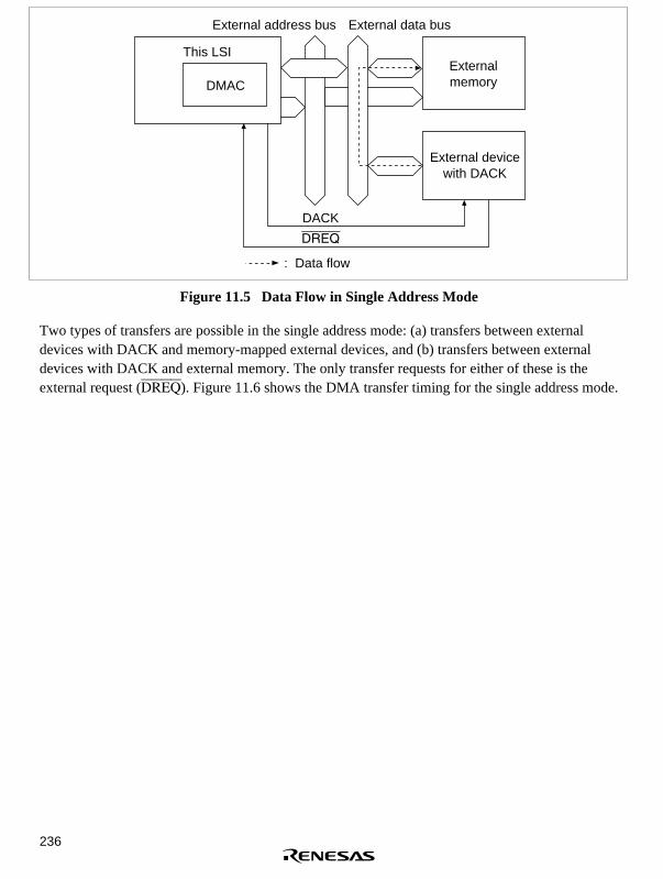
236
DMAC
DACK
DREQ
Externalmemory
External devicewith DACK
This LSI
External address bus
: Data flow
External data bus
Figure 11.5 Data Flow in Single Address Mode
Two types of transfers are possible in the single address mode: (a) transfers between externaldevices with DACK and memory-mapped external devices, and (b) transfers between externaldevices with DACK and external memory. The only transfer requests for either of these is theexternal request (DREQ). Figure 11.6 shows the DMA transfer timing for the single address mode.

237
CK
A21–A0
CSn
D15–D0
DACK
WRHWRL
Address output to external memory space
Data that is output from the externaldevice with DACK
DACK signal to external devices withDACK (active low)
WR signal to external memory space
a. External device with DACK to external memory space
CK
A21–A0
CSn
D15–D0
RD
Address output to external memory space
Data that is output from external memory space
RD signal to external memory space
DACK signal to external device with DACK (active low)
DACK
b. External memory space to external device with DACK
Figure 11.6 Example of DMA Transfer Timing in the Single Address Mode
11.3.6 Dual Address Mode
Dual address mode is used for access of both the transfer source and destination by address.Transfer source and destination can be accessed either internally or externally. Dual address modeis subdivided into two other modes: direct address transfer mode and indirect address transfermode.
Direct Address Transfer Mode: Data is read from the transfer source during the data read cycle,and written to the transfer destination during the write cycle, so transfer is conducted in two buscycles. At this time, the transfer data is temporarily stored in the DMAC. With the kind of externalmemory transfer shown in figure 11.7, data is read from one of the memories by the DMACduring a read cycle, then written to the other external memory during the subsequent write cycle.Figure 11.8 shows the timing for this operation.

238
Data buffer
Add
ress
bus
Dat
a bu
s
Add
ress
bus
Dat
a bu
s
Memory
Transfer source module
Transfer destination module
Memory
Transfer source module
Transfer destination module
SAR
DAR
Data buffer
SAR
DAR
The SAR value is taken as the address, and data is read from the transfer sourcemodule and stored temporarily in the DMAC.
1st bus cycle
2nd bus cycle
The DAR value is taken as the address, and data stored in the DMAC's data buffer is written to the transfer destination module.
DMAC
DMAC
Figure 11.7 Direct Address Operation during Dual Address Mode

239
Data read cycle
Data write cycle
Transfer destination address
Transfer source address
CK
(1st cycle) (2nd cycle)
A21–A0
CSn
D15–D0
RD
WRH, WRL
DACK
Note: Transfer between external memories with DACK are output during read cycle.
Figure 11.8 Example of Direct Address Transfer Timing in Dual Address Mode

240
Indirect Address Transfer Mode: In this mode the memory address storing the data you actuallywant to transfer is specified in DMAC internal transfer source address register (SAR3). Therefore,in indirect address transfer mode, the DMAC internal transfer source address register value is readfirst. This value is stored once in the DMAC. Next, the read value is output as the address, and thevalue stored at that address is again stored in the DMAC. Finally, the subsequent read value iswritten to the address specified by the transfer destination address register, ending one cycle ofDMA transfer.
In indirect address mode (figure 11.9), transfer destination, transfer source, and indirect addressstorage destination are all 16-bit external memory locations, and transfer in this example isconducted in 16-bit or 8-bit units. Timing for this transfer example is shown in figure 11.10.
In indirect address mode, one NOP cycle (figure 11.10) is required until the data read as theindirect address is output to the address bus. When transfer data is 32-bit, the third and fourth buscycles each need to be doubled, giving a required total of six bus cycles and one NOP cycle for thewhole operation.

241
SAR3
DAR3
Databuffer
Add
ress
bus
Dat
a bu
s
Memory
Transfer sourcemodule
Transfer destination module
Temporarybuffer
The SAR3 value is taken as the address, memory data is read, and the value is stored in thetemporary buffer. Since the value read at this time is used as the address, it must be 32 bits.When external connection data bus is 16 bits, two bus cycles are required.
DMAC
SAR3
DAR3
Databuffer
Add
ress
bus
Dat
a bu
s
Memory
Transfer sourcemodule
Transfer destination module
Temporarybuffer
The value in the temporary buffer is taken as the address, and data is read from the transfer source module to the data buffer.
SAR3
DAR3
Databuffer
Add
ress
bus
Dat
a bu
s
Memory
Transfer sourcemodule
Transfer destination module
Temporarybuffer
The DAR3 value is taken as the address, and the value in the data buffer is written to thetransfer destination module.Note: Memory, transfer source, and transfer destination modules are shown here.
In practice, connection can be made anywhere there is address space.
DMAC
DMAC
1st, 2nd bus cycles
3rd bus cycle
4th bus cycle
Figure 11.9 Dual Address Mode and Indirect Address Operation(When External Memory Space is 16 bits)

242
Transfersource
address (H)
Transfersource
address (L)
Indirectaddress
NOPTransfer
destinationaddress
Indirectaddress (H)
Indirectaddress (L)
Transfer data
Transfer data
Transfer data
Transfer data
Transfer data
Transfer sourceaddress *1
Indirect address *2
Indirect addressNOP
Indirect address
Address read cycle
(1st) (2nd) (3rd)
NOPcycle
Data read cycle
(4th)
Data write cycle
CK
A21–A0
CSn
D15–D0
Internaladdress
bus
Internal data bus
DMACindirect
addressbuffer
DMACdata
buffer
RD
WRH,WRL
Notes:*1*2
The internal address bus is controlled by the port and does not change.DMAC does not fetch value until 32-bit data is read from the internal data bus.
External memory space has 16-bit width.
Figure 11.10 Dual Address Mode and Indirect Address Transfer Timing Example 1(External Memory Space to External Memory Space)

243
Figure 11.11 shows an example of timing in indirect address mode when transfer source andindirect address storage locations are in internal memory, the transfer destination is an on-chipperipheral module with 2-cycle access space, and transfer data is 8-bit.
Since the indirect address storage destination and the transfer source are in internal memory, thesecan be accessed in one cycle. The transfer destination is 2-cycle access space, so two data writecycles are required. One NOP cycle is required until the data read as the indirect address is outputto the address bus.
Internaladdress
bus
Internaldatabus
DMACindirect address
buffer
DMACdata
buffer
CK
Transfer source address
NOP
NOP
Indirectaddress
Transfer destination
address
Indirect address
Indirect address
Transferdata
Transfer data
Transfer data
Addressread cycle
NOPcycle
Dataread cycle Data write cycle (4th)
(1st) (2nd) (3rd)
Figure 11.11 Dual Address Mode and Indirect Address Transfer Timing Example 2(On-chip Memory Space to On-chip Memory Space)

244
11.3.7 Bus Modes
Select the appropriate bus mode in the TM bits of CHCR0–CHCR3. There are two bus modes:cycle steal and burst.
Cycle-Steal Mode: In the cycle steal mode, the bus right is given to another bus master after eachone-transfer-unit (byte, word, or longword) DMAC transfer. When the next transfer requestoccurs, the bus rights are obtained from the other bus master and a transfer is performed for onetransfer unit. When that transfer ends, the bus right is passed to the other bus master. This isrepeated until the transfer end conditions are satisfied.
The cycle steal mode can be used with all categories of transfer destination, transfer source andtransfer request. Figure 11.12 shows an example of DMA transfer timing in the cycle steal mode.Transfer conditions are dual address mode and DREQ level detection.
CPU CPU CPU DMAC DMAC CPU DMAC DMAC CPU CPU
DREQ
Bus cycle
Bus control returned to CPU
Read Write WriteRead
Figure 11.12 DMA Transfer Example in the Cycle-Steal Mode
Burst Mode: Once the bus right is obtained, the transfer is performed continuously until thetransfer end condition is satisfied. In the external request mode with low level detection of theDREQ pin, however, when the DREQ pin is driven high, the bus passes to the other bus masterafter the bus cycle of the DMAC that currently has an acknowledged request ends, even if thetransfer end conditions have not been satisfied.
Figure 11.13 shows an example of DMA transfer timing in the burst mode. Transfer conditions aresingle address mode and DREQ level detection.
CPU CPU CPU DMAC DMAC DMAC DMAC DMAC
DREQ
Bus cycle DMAC CPU
Figure 11.13 DMA Transfer Example in the Burst Mode
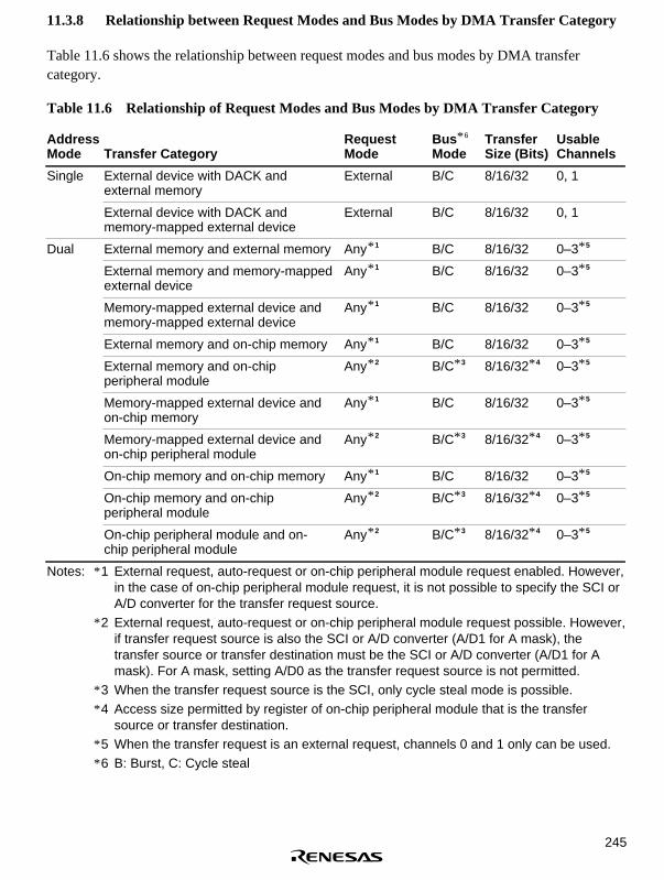
245
11.3.8 Relationship between Request Modes and Bus Modes by DMA Transfer Category
Table 11.6 shows the relationship between request modes and bus modes by DMA transfercategory.
Table 11.6 Relationship of Request Modes and Bus Modes by DMA Transfer Category
AddressMode Transfer Category
RequestMode
Bus * 6
ModeTransferSize (Bits)
UsableChannels
Single External device with DACK andexternal memory
External B/C 8/16/32 0, 1
External device with DACK andmemory-mapped external device
External B/C 8/16/32 0, 1
Dual External memory and external memory Any* 1 B/C 8/16/32 0–3* 5
External memory and memory-mappedexternal device
Any* 1 B/C 8/16/32 0–3* 5
Memory-mapped external device andmemory-mapped external device
Any* 1 B/C 8/16/32 0–3* 5
External memory and on-chip memory Any* 1 B/C 8/16/32 0–3* 5
External memory and on-chipperipheral module
Any* 2 B/C* 3 8/16/32* 4 0–3* 5
Memory-mapped external device andon-chip memory
Any* 1 B/C 8/16/32 0–3* 5
Memory-mapped external device andon-chip peripheral module
Any* 2 B/C* 3 8/16/32* 4 0–3* 5
On-chip memory and on-chip memory Any* 1 B/C 8/16/32 0–3* 5
On-chip memory and on-chipperipheral module
Any* 2 B/C* 3 8/16/32* 4 0–3* 5
On-chip peripheral module and on-chip peripheral module
Any* 2 B/C* 3 8/16/32* 4 0–3* 5
Notes: * 1 External request, auto-request or on-chip peripheral module request enabled. However,in the case of on-chip peripheral module request, it is not possible to specify the SCI orA/D converter for the transfer request source.
* 2 External request, auto-request or on-chip peripheral module request possible. However,if transfer request source is also the SCI or A/D converter (A/D1 for A mask), thetransfer source or transfer destination must be the SCI or A/D converter (A/D1 for Amask). For A mask, setting A/D0 as the transfer request source is not permitted.
* 3 When the transfer request source is the SCI, only cycle steal mode is possible.* 4 Access size permitted by register of on-chip peripheral module that is the transfer
source or transfer destination.* 5 When the transfer request is an external request, channels 0 and 1 only can be used.* 6 B: Burst, C: Cycle steal

246
11.3.9 Bus Mode and Channel Priority Order
When a given channel is transferring in burst mode, and a transfer request is issued to channel 0,which has a higher priority ranking, transfer on channel 0 begins immediately. If the priority levelsetting is fixed mode (CH0 > CH1), channel 1 transfer is continued after transfer on channel 0 arecompletely ended, whether the channel 0 setting is cycle steal mode or burst mode.
When the priority level setting is for round robin mode, transfer on channel 1 begins after transferof one transfer unit on channel 0, whether channel 0 is set to cycle steal mode or burst mode.Thereafter, bus right alternates in the order: channel 1 > channel 0 > channel 1 > channel 0.Whether the priority level setting is for fixed mode or round robin mode, since channel 1 is set toburst mode, the bus right is not given to the CPU. An example of round robin mode is shown infigure 11.14.
CPU DMACch1
DMACch1
DMACch0
DMACch1
DMACch0
DMACch1
DMACch1
CPU
ch0 ch1 ch0
DMAC ch0 and ch1round-robin mode
DMAC ch1burst mode CPUCPU
Priority: Round-robin modech0: Cycle-steal mode ch1: Burst mode
DMAC ch1burst mode
Figure 11.14 Bus Handling when Multiple Channels Are Operating
11.3.10 Number of Bus Cycle States and DREQ Pin Sample Timing
Number of States in Bus Cycle: The number of states in the bus cycle when the DMAC is thebus master is controlled by the bus state controller (BSC) just as it is when the CPU is the busmaster. For details, see section 10, Bus State Controller (BSC).
DREQ Pin Sampling Timing and DRAK Signal: In external request mode, the DREQ pin issampled by either falling edge or low-level detection. When a DREQ input is detected, a DMACbus cycle is issued and DMA transfer effected, at the earliest, after three states. However, in burstmode when single address operation is specified, a dummy cycle is inserted for the first bus cycle.In this case, the actual data transfer starts from the second bus cycle. Data is transferredcontinuously from the second bus cycle. The dummy cycle is not counted in the number oftransfer cycles, so there is no need to recognize the dummy cycle when setting the TCR.
DREQ sampling from the second time begins from the start of the transfer one bus cycle prior tothe DMAC transfer generated by the previous sampling.

247
DRAK is output once for the first DREQ sampling, irrespective of transfer mode or DREQdetection method. In burst mode, using edge detection, DREQ is sampled for the first cycle only,so DRAK is also output for the first cycle only. Therefore, the DREQ signal negate timing can beascertained, and this facilitates handshake operations of transfer requests with the DMAC.
Cycle Steal Mode Operations: In cycle steal mode, DREQ sampling timing is the sameirrespective of dual or single address mode, or whether edge or low-level DREQ detection is used.
For example, DMAC transfer begins (figure 11.15), at the earliest, three cycles from the firstsampling timing. The second sampling begins at the start of the transfer one bus cycle prior to thestart of the DMAC transfer initiated by the first sampling (i.e., from the start of the CPU(3)transfer). At this point, if DREQ detection has not occurred, sampling is executed every cyclethereafter.
As in figure 11.16, whatever cycle the CPU transfer cycle is, the next sampling begins from thestart of the transfer one bus cycle before the DMAC transfer begins.
Figure 11.15 shows an example of output during DACK read and figure 11.16 an example ofoutput during DACK write.

248
CK
DR
EQ
DR
AK
Bus
cy
cle
DA
CK
CP
U(3
)C
PU
(4)
CP
U(5
)
CP
U(2
)C
PU
(1)1s
t sam
plin
g2n
d sa
mpl
ing
DM
AC
(R)
DM
AC
(R)
DM
AC
(W)
DM
AC
(W)
DM
AC
(W)
DM
AC
(R)
Figure 11.15 Cycle Steal, Dual Address, and Level Detection (Fastest Operation)

249
CK
DR
EQ
DR
AK
Bus
cy
cle
DA
CK
CP
UC
PU
CP
UC
PU
DM
AC
(R)
DM
AC
(R
)
DM
AC
(W)
1st s
ampl
ing
2nd
sam
plin
g
Not
e:W
ith c
ycle
-ste
al a
nd d
ual a
ddre
ss o
pera
tion,
sam
plin
g tim
ing
is th
e sa
me
w
heth
er D
RE
Q d
etec
tion
is b
y le
vel o
r by
edg
e.
Figure 11.16 Cycle Steal, Dual Address, and Level Detection (Normal Operation)

250
Figures 11.17 and 11.18 show cycle steal mode and single address mode. In this case, transferbegins at earliest three cycles after the first DREQ sampling. The second sampling begins from thestart of the transfer one bus cycle before the start of the first DMAC transfer. In single addressmode, the DACK signal is output during the DMAC transfer period.

251
CK
DR
EQ
DR
AK
Bus
cy
cle
DA
CK
CP
UC
PU
CP
U
CP
UC
PU
DM
AC
DM
AC
DM
AC
Figure 11.17 Cycle Steal, Single Address, and Level Detection (Fastest Operation)

252
CK
DR
EQ
DR
AK
Bus
cy
cle
DA
CK
CP
UC
PU
DM
AC
CP
UD
MA
CC
PU
C
PU
Figure 11.18 Cycle Steal, Single Address, and Level Detection (Normal Operation)

253
Burst Mode, Dual Address, and Level Detection: DREQ sampling timing in burst mode withdual address and level detection is virtually the same as that of cycle steal mode.
For example, DMAC transfer begins (figure 11.19), at the earliest, three cycles after the timing ofthe first sampling. The second sampling also begins from the start of the transfer one bus cyclebefore the start of the first DMAC transfer. In burst mode, as long as transfer requests are issued,DMAC transfer continues. Therefore, the “transfer one bus cycle before the start of the DMACtransfer” may be a DMAC transfer.
In burst mode, the DACK output period is the same as that of cycle steal mode. Figure 11.20shows the normal operation of this burst mode.

254
CK
DR
EQ
DR
AK
Bus
cy
cle
DA
CK
CP
U
C
PU
C
PU
CP
UD
MA
C(R
)D
MA
C(W
)D
MA
C(R
)D
MA
C(R
)
DM
AC
(W)
DM
AC
(R)
DM
AC
(W)
Figure 11.19 Burst Mode, Dual Address, and Level Detection (Fastest Operation)

255
CK
DR
EQ
DR
AK
Bus
cy
cle
DA
CK
CP
UC
PU
DM
AC
(R)
DM
AC
(R)
DM
AC
(R)
C
PU
DM
AC
(W)
DM
AC
(W)
Figure 11.20 Burst Mode, Dual Address, and Level Detection (Normal Operation)

256
Burst Mode, Single Address, and Level Detection: DREQ sampling timing in burst mode withsingle address and level detection is shown in figures 11.21 and 11.22.
In burst mode with single address and level detection, a dummy cycle is inserted as one bus cycle,at the earliest, three cycles after timing of the first sampling. Data during this period is undefined,and the DACK signal is not output. Nor is the number of DMAC transfers counted. The actualDMAC transfer begins after one dummy bus cycle output.
The dummy cycle is not counted either at the start of the second sampling (transfer one bus cyclebefore the start of the first DMAC transfer). Therefore, the second sampling is not conducted fromthe bus cycle starting the dummy cycle, but from the start of the CPU(3) bus cycle.
Thereafter, as long the DREQ is continuously sampled, no dummy cycle is inserted. DREQsampling timing during this period begins from the start of the transfer one bus cycle before thestart of DMAC transfer, in the same way as with cycle steal mode.
As with the fourth sampling in figure 11.21, once DMAC transfer is interrupted, a dummy cycle isagain inserted at the start as soon as DMAC transfer is resumed.
The DACK output period in burst mode is the same as in cycle steal mode.

257
CK
DR
EQ
DR
AK
Bus
cy
cle
DA
CK
CP
U(4
)C
PU
(1)
CP
U(2
)C
PU
(3)
Dum
my
DM
AC
Dum
my
2nd
sam
plin
g1s
t sa
mpl
ing
3rd
sam
plin
g4t
h sa
mpl
ing
DM
AC
DM
AC
Figure 11.21 Burst Mode, Single Address, and Level Detection (Fastest Operation)

258
CK
DR
EQ
DR
AK
Bus
cy
cle
DA
CK
CP
UC
PU
Dum
my
DM
AC
C
PU
DM
AC
DM
AC
Figure 11.22 Burst Mode, Single Address, and Level Detection (Normal Operation)

259
Burst Mode, Dual Address, and Edge Detection: In burst mode with dual address and edgedetection, DREQ sampling is conducted only on the first cycle.
In figure 11.23, DMAC transfer begins, at the earliest, three cycles after the timing of the firstsampling. Thereafter, DMAC transfer continues until the end of the data transfer count set in theTCR. DREQ sampling is not conducted during this period. Therefore, DRAK is output on the firstcycle only.
When DMAC transfer is resumed after being halted by a NMI or address error, be sure to reinputan edge request. The remaining transfer restarts after the first DRAK output.
The DACK output period in burst mode is the same as in cycle steal mode.

260
CK
DR
EQ
DR
AK
Bus
cy
cle
DA
CK
CP
U
C
PU
CP
UD
MA
C(R
)
DM
AC
(R)
DM
AC
(R)
DM
AC
(R)
DM
AC
(W)
DM
AC
(W)
DM
AC
(W)
DM
AC
(W)
Figure 11.23 Burst Mode, Dual Address, and Edge Detection

261
Burst Mode, Single Address, and Edge Detection: In burst mode with single address and edgedetection, DREQ sampling is conducted only on the first cycle. In figure 11.24, a dummy cycle isinserted, at the earliest, three cycles after the timing for the first sampling. During this period, datais undefined, and DACK is not output. Nor is the number of DMAC transfers counted. Thereafter,DMAC transfer continues until the data transfer count set in the DMATCR has ended. DREQsampling is not conducted during this period. Therefore, DRAK is output on the first cycle only.
When DMAC transfer is resumed after being halted by a NMI or address error, be sure to reinputan edge request. DRAK is output once, and the remaining transfer restarts after output of onedummy cycle.
The DACK output period in burst mode is the same as in cycle steal mode.

262
CK
DR
EQ
DR
AK
Bus
cy
cle
DA
CK
CP
UD
MA
CD
MA
CD
MA
CD
MA
C
C
PU
CP
U
D
umm
y
Figure 11.24 Burst Mode, Single Address and Edge Detection
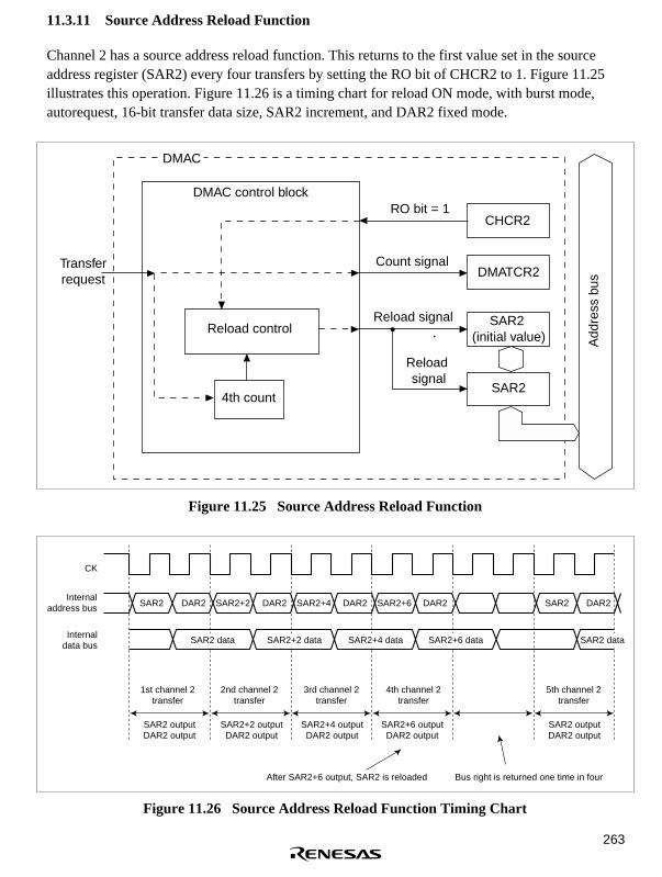
263
11.3.11 Source Address Reload Function
Channel 2 has a source address reload function. This returns to the first value set in the sourceaddress register (SAR2) every four transfers by setting the RO bit of CHCR2 to 1. Figure 11.25illustrates this operation. Figure 11.26 is a timing chart for reload ON mode, with burst mode,autorequest, 16-bit transfer data size, SAR2 increment, and DAR2 fixed mode.
SAR2 (initial value)
DMAC
Transferrequest
DMAC control block
Reload control
4th count
CHCR2
DMATCR2
SAR2
RO bit = 1
Count signal
Reload signal
Reload signal
Add
ress
bus
Figure 11.25 Source Address Reload Function
CK
Internaladdress bus
Internaldata bus
SAR2 DAR2 DAR2 DAR2 DAR2SAR2+2 SAR2+4 SAR2+6 SAR2 DAR2
SAR2 data SAR2+2 data SAR2+4 data SAR2+6 data SAR2 data
1st channel 2transfer
2nd channel 2transfer
3rd channel 2transfer
4th channel 2transfer
5th channel 2transfer
SAR2 outputDAR2 output
SAR2+2 outputDAR2 output
SAR2+4 outputDAR2 output
SAR2+6 outputDAR2 output
SAR2 outputDAR2 output
After SAR2+6 output, SAR2 is reloaded Bus right is returned one time in four
Figure 11.26 Source Address Reload Function Timing Chart

264
The reload function can be executed whether the transfer data size is 8, 16, or 32 bits.
DMATCR2, which specifies the number of transfers, is decremented by 1 at the end of everysingle-transfer-unit transfer, regardless of whether the reload function is on or off. Therefore,when using the reload function in the on state, a multiple of 4 must be specified in DMATCR2.Operation will not be guaranteed if any other value is set. Also, the counter which counts theoccurrence of four transfers for address reloading is reset by clearing of the DME bit in DMAORor the DE bit in CHCR2, setting of the transfer end flag (the TE bit in CHCR2), NMI input, andsetting of the AE flag (address error generation in DMAC transfer), as well as by a reset and insoftware standby mode, but SAR2, DAR2, DMATCR2, and other registers are not reset.Consequently, when one of these sources occurs, there is a mixture of initialized counters anduninitialized registers in the DMAC, and incorrect operation may result if a restart is executed inthis state. Therefore, when one of the above sources, other than TE setting, occurs during use ofthe address reload function, SAR, DAR2, and DMATCR2 settings must be carried out before re-execution.
11.3.12 DMA Transfer Ending Conditions
The DMA transfer ending conditions vary for individual channels ending and for all channelsending together.
Individual Channel Ending Conditions: There are two ending conditions. A transfer ends whenthe value of the channel’s DMA transfer count register (DMATCR) is 0, or when the DE bit of thechannel’s CHCR is cleared to 0.
• When DMATCR is 0: When the DMATCR value becomes 0 and the corresponding channel'sDMA transfer ends, the transfer end flag bit (TE) is set in the CHCR. If the IE (interruptenable) bit has been set, a DMAC interrupt (DEI) is requested of the CPU.
• When DE of CHCR is 0: Software can halt a DMA transfer by clearing the DE bit in thechannel’s CHCR. The TE bit is not set when this happens.
Conditions for Ending All Channels Simultaneously: Transfers on all channels end when theNMIF (NMI flag) bit or AE (address error flag) bit is set to 1 in the DMAOR, or when the DMEbit in the DMAOR is cleared to 0.
• When the NMIF or AE bit is set to 1 in DMAOR: When an NMI interrupt or DMAC addresserror occurs, the NMIF or AE bit is set to 1 in the DMAOR and all channels stop theirtransfers. The DMAC obtains the bus rights, and if these flags are set to 1 during execution ofa transfer, DMAC halts operation when the transfer processing currently being executed ends,and transfers the bus right to the other bus master. Consequently, even if the NMIF or AE bitsare set to 1 during a transfer, the DMA source address register (SAR), designation addressregister (DAR), and transfer count register (TCR) are all updated. The TE bit is not set. Toresume the transfers after NMI interrupt or address error processing, clear the appropriate flagbit to 0. To avoid restarting a transfer on a particular channel, clear its DE bit to 0.

265
When the processing of a one unit transfer is complete. In a dual address mode direct addresstransfer, even if an address error occurs or the NMI flag is set during read processing, thetransfer will not be halted until after completion of the following write processing. In such acase, SAR, DAR, and TCR values are updated. In the same manner, the transfer is not halted indual address mode indirect address transfers until after the final write processing has ended.
• When DME is cleared to 0 in DMAOR: Clearing the DME bit to 0 in the DMAOR aborts thetransfers on all channels. The TE bit is not set.
11.3.13 DMAC Access from CPU
The space addressed by the DMAC is 3-cycle space. Therefore, when the CPU becomes the busmaster and accesses the DMAC, a minimum of three basic clock (CLK) cycles are required forone bus cycle. Also, since the DMAC is located in word space, while a word-size access to theDMAC is completed in one bus cycle, a longword-size access is automatically divided into twoword accesses, requiring two bus cycles (six basic clock cycles). These two bus cycles areexecuted consecutively; a different bus cycle is never inserted between the two word accesses.This applies to both write accesses and read accesses.
11.4 Examples of Use
11.4.1 Example of DMA Transfer between On-Chip SCI and External Memory
In this example, on-chip serial communication interface channel 0 (SCI0) received data istransferred to external memory using the DMAC channel 3.
Table 11.7 indicates the transfer conditions and the setting values of each of the registers.
Table 11.7 Transfer Conditions and Register Set Values for Transfer between On-ChipSCI and External Memory
Transfer Conditions Register Value
Transfer source: RDR0 of on-chip SCI0 SAR3 H'FFFF81A5
Transfer destination: external memory DAR3 H'00400000
Transfer count: 64 times DMATCR3 H'00000040
Transfer source address: fixed CHCR3 H'00004D05
Transfer destination address: incremented
Transfer request source: SCI0 (RDR0)
Bus mode: cycle steal
Transfer unit: byte
Interrupt request generation at end of transfer
Channel priority ranking: 0 > 1 > 2 > 3 DMAOR H'0001

266
11.4.2 Example of DMA Transfer between External RAM and External Device with
DACK
In this example, an external request, serial address mode transfer with external memory as thetransfer source and an external device with DACK as the transfer destination is executed usingDMAC channel 1.
Table 11.8 indicates the transfer conditions and the setting values of each of the registers.
Table 11.8 Transfer Conditions and Register Set Values for Transfer between ExternalRAM and External Device with DACK
Transfer Conditions Register Value
Transfer source: external RAM SAR1 H'00400000
Transfer destination: external device with DACK DAR1 (access by DACK)
Transfer count: 32 times DMATCR1 H'00000020
Transfer source address: decremented CHCR1 H'00002269
Transfer destination address: (setting ineffective)
Transfer request source: external pin (DREQ1) edgedetection
Bus mode: burst
Transfer unit: word
No interrupt request generation at end of transfer
Channel priority ranking: 2 > 0 > 1 > 3 DMAOR H'0201
11.4.3 Example of DMA Transfer between A/D Converter and On-Chip Memory
(Address Reload On) (Excluding A Mask)
In this example, the on-chip A/D converter channel 0 is the transfer source and on-chip memory isthe transfer destination, and the address reload function is on.
Table 11.9 indicates the transfer conditions and the setting values of each of the registers.

267
Table 11.9 Transfer Conditions and Register Set Values for Transfer between A/DConverter and On-Chip Memory
Transfer Conditions Register Value
Transfer source: on-chip A/D converter ch0 SAR2 H'FFFF83F0
Transfer destination: on-chip memory DAR2 H'FFFFF000
Transfer count: 128 times (reload count 32 times) DMATCR2 H'00000080
Transfer source address: incremented CHCR2 H'00085B25
Transfer destination address: incremented
Transfer request source: A/D converter
Bus mode: burst
Transfer unit: byte
Interrupt request generation at end of transfer
Channel priority ranking: 0 > 2 > 3 > 1 DMAOR H'0101
When address reload is on, the SAR value returns to its initially established value every fourtransfers. In the above example, when a transfer request is input from the A/D converter, the bytesize data is first read in from the H'FFFF83F0 register of AD0 and that data is written to the on-chip memory address H'FFFFF001. Because a byte size transfer was performed, the SAR andDAR values at this point are H'FFFF83F1 and H'FFFFF001, respectively. Also, because this is aburst transfer, the bus rights remain secured, so continuous data transfer is possible.
When four transfers are completed, if the address reload is off, execution continues with the fifthand sixth transfers and the SAR value continues to increment from H'FFFF83F3 to H'FFFF83F4 toH'FFFF83F5 and so on. However, when the address reload is on, the DMAC transfer is haltedupon completion of the fourth one and the bus right request signal to the CPU is cleared. At thistime, the value stored in SAR is not H'FFFF83F3–H'FFFF83F4, but H'FFFF83F3–H'FFFF83F0, areturn to the initially established address. The DAR value always continues to be decrementedregardless of whether the address reload is on or off.
The DMAC internal status, due to the above operation after completion of the fourth transfer, isindicated in table 11.10 for both address reload on and off.

268
Table 11.10 DMAC Internal Status
Item Address Reload On Address Reload Off
SAR H'FFFF83F0 H'FFFF83F4
DAR H'FFFFF004 H'FFFFF004
DMATCR H'0000007C H'0000007C
Bus rights Released Maintained
DMAC operation Halted Processing continues
Interrupts Not issued Not issued
Transfer request source flag clear Executed Not executed
Notes: 1. Interrupts are executed until the DMATCR value becomes 0, and if the IE bit of theCHCR is set to 1, are issued regardless of whether the address reload is on or off.
2. If transfer request source flag clears are executed until the DMATCR value becomes 0,they are executed regardless of whether the address reload is on or off.
3. Designate burst mode when using the address reload function. There are cases whereabnormal operation will result if it is executed in cycle steal mode.
4. Designate a multiple of four for the TCR value when using the address reload function.There are cases where abnormal operation will result if anything else is designated.
To execute transfers after the fifth one when the address reload is on, make the transfer requestsource issue another transfer request signal.
11.4.4 Example of DMA Transfer between A/D Converter and Internal Memory (Address
Reload On) (A Mask)
In this example the on-chip A/D converter (A/D1) is the transfer source and the internal memory isthe transfer destination, and the address reload on.
Table 11.11 indicates the transfer conditions and the setting values of each of the registers.

269
Table 11.11 Transfer Conditions and Register Set Values for Transfer between A/DConverter (A/D1) and Internal Memory
Transfer Conditions Register Value
Transfer source: on-chip A/D converter (A/D1) SAR2 H'FFFF8408
Transfer destination: internal memory DAR2 H'FFFFF000
Transfer count: 128 times (reload count 32 times) DMATCR2 H'00000080
Transfer source address: incremented CHCR2 H'00085B25
Transfer target address: incremented
Transfer request source: A/D converter (A/D1)
Bus mode: burst
Transfer unit: byte
Interrupt request generated at end of transfer
Channel priority sequence: 0>2>3>1 DMAOR H'0101
When address reload is on, the SAR value returns to its initially established value every fourtransfers. In the above example, when a transfer request is input from the A/D converter (A/D1),the byte size data is first read in from the H'FFFF8408 register and that data is written to the on-chip memory address H'FFFFF001. Because a byte size transfer was performed, the SAR andDAR values at this point are H'FFFF8409 and H'FFFFF001, respectively. Also, because this is aburst transfer, the bus rights remain secured, so continuous data transfer is possible.
When four transfers are completed, if the address reload is off, execution continues with the fifthand sixth transfers and the SAR value continues to increment from H'FFFF840B to H'FFFF840Cto H'FFFF840D and so on. However, when the address reload is on, the DMAC transfer is haltedupon completion of the fourth transfer and the bus right request signal to the CPU is cleared. Atthis time, the values stored in SAR are not H'FFFF840B–H'FFFF840C, but H'FFFF840B–H'FFFF8408, a return to the initially established address. The DAR value always continues to bedecremented regardless of whether the address reload is on or off.
The DMAC internal status, due to the above operation after completion of the fourth transfer, isindicated in table 11.12 for both address reload on and off.

270
Table 11.12 DMAC Internal Status
Item Address Reload On Address Reload Off
SAR H'FFFF8408 H'FFFF840C
DAR H'FFFFF004 H'FFFFF004
DMATCR H'0000007C H'0000007C
Bus rights Released Maintained
DMAC operation Halted Processing continues
Interrupts Not issued Not issued
Transfer request source flag clear Executed Not executed
Notes: 1. Interrupts are executed until the DMATCR value becomes 0, and if the IE bit of theCHCR is set to 1, are issued regardless of whether the address reload is on or off.
2. If transfer request source flag clears are executed until the DMATCR value becomes 0,they are executed regardless of whether the address reload is on or off.
3. Designate burst mode when using the address reload function. There are cases whereabnormal operation will result if it is executed in cycle steal mode.
4. Designate a multiple of four for the TCR value when using the address reload function.There are cases where abnormal operation will result if anything else is designated.
To execute more than four transfers with the address reload on, make the transfer request sourceissue another transfer request signal.
11.4.5 Example of DMA Transfer between External Memory and SCI1 Send Side
(Indirect Address On)
In this example, DMAC channel 3 is used, an indirect address designated external memory is thetransfer source and the SCI1 sending side is the transfer destination.
Table 11.13 indicates the transfer conditions and the setting values of each of the registers.

271
Table 11.13 Transfer Conditions and Register Set Values for Transfer between ExternalMemory and SCI1 Sending Side
Transfer Conditions Register Value
Transfer source: external memory SAR3 H'00400000
Value stored in address H'00400000 — H'00450000
Value stored in address H'00450000 — H'55
Transfer destination: on-chip SCI TDR1 DAR3 H'FFFF81B3
Transfer count: 10 times DMATCR3 H'0000000A
Transfer source address: incremented CHCR3 H'00011E01
Transfer destination address: fixed
Transfer request source: SCI1 (TDR1)
Bus mode: cycle steal
Transfer unit: byte
Interrupt request not generated at end of transfer
Channel priority ranking: 0 > 1 > 2 > 3 DMAOR H'0001
When indirect address mode is on, the data stored in the address established in SAR is not used asthe transfer source data. In the case of indirect addressing, the value stored in the SAR address isread, then that value is used as the address and the data read from that address is used as thetransfer source data, then that data is stored in the address designated by the DAR.
In the table 11.13 example, when a transfer request from the TDR1 of SCI1 is generated, a read ofthe address located at H'00400000, which is the value set in SAR3, is performed first. The dataH'00450000 is stored at this H'00400000 address, and the DMAC first reads this H'00450000value. It then uses this read value of H'00450000 as an address and reads the value of H'55 that isstored in the H'00450000 address. It then writes the value H'55 to the address H'FFFF81B3designated by DAR3 to complete one indirect address transfer.
With indirect addressing, the first executed data read from the address established in SAR3 alwaysresults in a longword size transfer regardless of the TS0, TS1 bit designations for transfer datasize. However, the transfer source address fixed and increment or decrement designations are asaccording to the SM0, SM1 bits. Consequently, despite the fact that the transfer data sizedesignation is byte in this example, the SAR3 value at the end of one transfer is H'00400004. Thewrite operation is exactly the same as an ordinary dual address transfer write operation.

272
11.5 Cautions on Use
1. Other than the DMA operation register (DMAOR) accessing in word (16-bit) units, access allregisters in word (16-bit) or longword (32-bit) units.
2. When rewriting the RS0–RS3 bits of CHCR0–CHCR3, first clear the DE bit to 0 (set the DEbit to 0 before doing rewrites with a CHCR byte address).
3. When an NMI interrupt is input, the NMIF bit of the DMAOR is set even when the DMAC isnot operating.
4. Set the DME bit of the DMAOR to 0 and make certain that any DMAC received transferrequest processing has been completed before entering standby mode.
5. Do not access the DMAC, DTC, BSC, or UBC on-chip peripheral modules from the DMAC.
6. When activating the DMAC, do the CHCR or DMAOR setting as the final step. There areinstances where abnormal operation will result if any other registers are established last.
7. After the DMATCR count becomes 0 and the DMA transfer ends normally, always write a 0 tothe DMATCR, even when executing the maximum number of transfers on the same channel.There are instances where abnormal operation will result if this is not done.
8. Designate burst mode as the transfer mode when using the address reload function. There areinstances where abnormal operation will result in cycle steal mode.
9. Designate a multiple of four for the DMATCR value when using the address reload function.There are instances where abnormal operation will result if anything else is designated.
10. When detecting external requests by falling edge, maintain the external request pin at highlevel when performing the DMAC establishment.
11. When operating in single address mode, establish an external address as the address. There areinstances where abnormal operation will result if an internal address is established.
12. Do not access DMAC register empty addresses (H'FFFF86B2–H'FFFF86BF). Operationcannot be guaranteed when empty addresses are accessed.

273
Section 12 Multifunction Timer Pulse Unit (MTU)
12.1 Overview
The SuperH microprocessor has an on-chip 16-bit multifunction timer pulse unit (MTU) with fivechannels of 16-bit timers.
12.1.1 Features
• Can process a maximum of sixteen different pulse outputs and inputs.
• Has sixteen timer general registers (TGR): four each for channels 0, 3, and 4, and two each forchannels 1 and 2 that can be set to function independently as output compare or input capture.The channel 0, 3, and 4 TGRC and TGRD registers can be used as buffer registers.
• Can select eight counter input clock sources for all channels
• All channels can be set for the following operating modes:
Compare match waveform output: 0 output/1 output/toggle output selectable.
Input capture function: Selectable rising edge, falling edge, or both rising and falling edgedetection.
Counter clearing function: Counters can be cleared by a compare-match or input capture.
Synchronizing mode: Two or more timer counters (TCNT) can be written tosimultaneously. Two or more timer counters can be simultaneously cleared by a compare-match or input capture. Counter synchronization functions enable synchronized registerinput/output.
PWM mode: PWM output can be provided with any duty cycle. When combined with thecounter synchronizing function, enables up to twelve-phase PWM output. (With channels0–2 set to PWM mode 2, channels 3–4, and channels 0–4 synchronized with TGR3A ofchannel 3 as the sync register (channels 0–4 phase output: 4, 2, 2, 2, 2).)
• Channels 0, 3, and 4 can be set for buffer operation
Input capture register double buffer configuration possible
Output compare register automatic re-write possible
• Channels 1 and 2 can be independently set to the phase counting mode
Two-phase encoder pulse up/down count possible
• Cascade connection operation
Can be operated as a 32-bit counter by using the channel 2 input clock for channel 1overflow/underflow
• Channels 3 and 4 can be set in the following modes:
Reset-synchronized PWM mode: By combining channels 3 and 4, a sawtooth wavecomparator type six-phase PWM waveform can be output.

274
Complementary PWM mode: By combining channels 3 and 4, a triangle wave comparatortype six-phase PWM output is possible with non-overlapping times.
• High speed access via internal 16-bit bus
• Twenty-three interrupt sources
Channels 0, 3, and 4 have four compare-match/input capture interrupts and one overflowinterrupt which can be requested independently.
Channels 1 and 2 have two compare-match/input capture interrupts, one overflow interrupt,and one underflow interrupt which can be requested independently.
• Automatic transfer of register data
Block transfer, 1-word data transfers and 1-byte data transfers are possible through DTC orDMAC activation.
• A/D converter conversion start trigger can be generated
Channels 0–4 compare-match/input capture signals can be used as A/D converterconversion start triggers.

275
Table 12.1 summarizes the MTU functions.
Table 12.1 MTU Functions
Item Channel 0 Channel 1 Channel 2 Channel 3 Channel 4
Counter clocks Internal: φ/1, φ/4, φ/16, φ/64, φ/256, φ/1024External: Eight to each channel from TCLKA, TCLKB, TCLKC, and TCLKD
General registers TGR0A
TGR0B
TGR1A
TGR1B
TGR2A
TGR2B
TGR3A
TGR3B
TGR4A
TGR4B
Generalregisters/bufferregisters
TGR0CTGR0D
No No TGR3CTGR3D
TGR4CTGR4D
Input/output pins TIOC0A
TIOC0B
TIOC0C
TIOC0D
TIOC1A
TIOC1B
TIOC2A
TIOC2B
TIOC3A
TIOC3B
TIOC3C
TIOC3D
TIOC4A
TIOC4B
TIOC4C
TIOC4D
Counter clearfunction
TGR compare-match or inputcapture
TGR compare-match or inputcapture
TGR compare-match or inputcapture
TGR compare-match or inputcapture
TGR compare-match or inputcapture
Compare 0 Yes Yes Yes Yes Yes
match output 1 Yes Yes Yes Yes Yes
Toggle Yes Yes Yes Yes Yes
Input capturefunction
Yes Yes Yes Yes Yes
Synchronization Yes Yes Yes Yes Yes
Buffer operation Yes No No Yes No
PWM mode 1 Yes Yes Yes Yes Yes
PWM mode 2 Yes Yes Yes No No
Phase countingmode
No Yes Yes No No
Reset-synchronizedPWM mode
No No No Yes Yes
ComplementaryPWM mode
No No No Yes Yes
DMAC activation TGR0A com-pare match orinput capture
TGR1A com-pare match orinput capture
TGR2A com-pare match orinput capture
TGR3A com-pare match orinput capture
TGR4A com-pare match orinput capture

276
Table 12.1 MTU Functions (cont)
Item Channel 0 Channel 1 Channel 2 Channel 3 Channel 4
Hard DTCactivation
TGR compare-match or inputcapture
TGR compare-match or inputcapture
TGR compare-match or inputcapture
TGR compare-match or inputcapture
TGR compare-match or inputcapture andTCNT4overflow/underflow
A/D conversion starttrigger
TGR0A com-pare match orinput capture
TGR1A com-pare match orinput capture
TGR2A com-pare match orinput capture
TGR3A com-pare match orinput capture
TGR4A com-pare match orinput capture
Interrupt sources Comparematch/inputcapture 0A
Comparematch/inputcapture 1A
Comparematch/inputcapture 2A
Comparematch/inputcapture 3A
Comparematch/inputcapture 4A
Comparematch/inputcapture 0B
Comparematch/inputcapture 1B
Comparematch/inputcapture 2B
Comparematch/inputcapture 3B
Comparematch/inputcapture 4B
Comparematch/inputcapture 0C
Overflow Overflow Comparematch/inputcapture 3C
Comparematch/inputcapture 4C
Comparematch/inputcapture 0D
Underflow Underflow Comparematch/inputcapture 3D
Comparematch/inputcapture 4D
Overflow — — Overflow Overflow/underflow
12.1.2 Block Diagram
Figure 12.1 is the block diagram of the MTU.

277
TC
R
Cha
nnel
0C
hann
el 1
Cha
nnel
2C
hann
el 4
Cha
nnel
3S
hare
d
Con
trol
logi
c
Cha
nnel
s 0–
2 co
ntro
l log
icC
hann
els
3, 4
con
trol
logi
c
TM
DR
TIO
RH
TIO
RL
TIE
RT
SR
TC
RT
MD
RT
IOR
TIE
RT
SR
TC
RT
MD
RT
IOR
TIE
RT
SR
TS
TR
TS
YR
TC
RT
MD
RT
IOR
TIO
RL
TIE
RT
SR
TC
RT
MD
RT
IOR
HT
IOR
LT
IER
TS
RT
OE
RT
OC
RT
GC
R
TC
NT
BU
S I/
FT
GR
A
TG
RD
TG
RB
TG
RC
TC
NT
S
TD
DR
TC
DR
TC
BR
TC
NT
TG
RA
TG
RD
TG
RB
TG
RC
TC
NT
TG
RA
TG
RB
TC
NT
TG
RA
TG
RB
TC
NT
TG
RA
TG
RD
TG
RB
TG
RC
(I/O pins)Channel 3:
TIOC3ATIOC3BTIOC3CTIOC3D
Channel 4:TIOC4ATIOC4BTIOC4CTIOC4D
(Clock input)Internal clock:
φ/1φ/4
φ/16φ/64
φ/256φ/1024
(I/O pins)Channel 0:
TIOC0ATIOC0BTIOC0CTIOC0D
External clock:TCLKATCLKBTCLKCTCLKD
Channel 1: TIOC1ATIOC1B
Channel 2: TIOC2ATIOC2B
Internal data bus
A/D conversionstart request signal
(Interruptrequest signals)Channel 3:TGI3ATGI3BTGI3CTGI3DTGI3V
Channel 4:TGI4ATGI4BTGI4CTGI4DTGI4V
(Interruptrequest signal)Channel 0:TGI0ATGI0BTGI0CTGI0DTGI0V
Channel 1:TGI1ATGI1BTGI1VTGI1U
Channel 2:TGI2ATGI2BTGI2VTGI2U
Mod
ule
data
bus
Figure 12.1 MTU Block Diagram

278
12.1.3 Pin Configuration
Table 12.2 summarizes the MTU pins.
Table 12.2 Pin Configuration
Channel Name Pin Name I/O Function
Shared Clock input A TCLKA I Clock A input pin (A-phase input pin in channel 1phase counting mode)
Clock input B TCLKB I Clock B input pin (B-phase input pin in channel 1phase counting mode)
Clock input C TCLKC I Clock C input pin (A-phase input pin in channel 2phase counting mode)
Clock input D TCLKD I Clock D input pin (B-phase input pin in channel 2phase counting mode)
0 Inputcapture/outputcompare-match 0A
TIOC0A I/O TGR0A input capture input/output compareoutput/PWM output pin
Inputcapture/outputcompare-match 0B
TIOC0B I/O TGR0B input capture input/output compareoutput/PWM output pin
Inputcapture/outputcompare-match 0C
TIOC0C I/O TGR0C input capture input/output compareoutput/PWM output pin
Inputcapture/outputcompare-match 0D
TIOC0D I/O TGR0D input capture input/output compareoutput/PWM output pin
1 Inputcapture/outputcompare-match 1A
TIOC1A I/O TGR1A input capture input/output compareoutput/PWM output pin
Inputcapture/outputcompare-match 1B
TIOC1B I/O TGR1B input capture input/output compareoutput/PWM output pin
2 Inputcapture/outputcompare-match 2A
TIOC2A I/O TGR2A input capture input/output compareoutput/PWM output pin
Inputcapture/outputcompare-match 2B
TIOC2B I/O TGR2B input capture input/output compareoutput/PWM output pin

279
Table 12.2 Pin Configuration (cont)
Channel Name Pin Name I/O Function
3 Inputcapture/outputcompare-match 3A
TIOC3A I/O TGR3A input capture input/output compareoutput/PWM output pin
In complementary PWM/reset synchronous PWMmode, 1/2 PWM period toggle output pin
Inputcapture/outputcompare-match 3B
TIOC3B I/O TGR3B input capture input/output compare outputpin
In complementary PWM/reset synchronous PWMmode, PWM output/U phase output pin
Inputcapture/outputcompare-match 3C
TIOC3C I/O TGR3C input capture input/output compareoutput/PWM output pin
In complementary PWM/reset synchronous PWMmode
Inputcapture/outputcompare-match 3D
TIOC3D I/O TGR3D input capture input/output compare outputpin
In complementary PWM/reset synchronous PWMmode, PWM output/U phase output pin
4 Inputcapture/outputcompare-match 4A
TIOC4A I/O TGR4A input capture input/output compareoutput/PWM output pin
In complementary PWM/reset synchronous PWMmode, PWM output/V phase output pin
Inputcapture/outputcompare-match 4B
TIOC4B I/O TGR4B input capture input/output compare outputpin
In complementary PWM/reset synchronous PWMmode, PWM output/W phase output pin
Inputcapture/outputcompare-match 4C
TIOC4C I/O TGR4C input capture input/output compareoutput/PWM output pin
In complementary PWM/reset synchronous PWMmode, PWM output/V phase output pin
Inputcapture/outputcompare-match 4D
TIOC4D I/O TGR4D input capture input/output compare outputpin
In complementary PWM/reset synchronous PWMmode, PWM output/W phase output pin
Note: The TIOC pins output undefined values when they are set to input capture and timer outputby the pin function controller (PFC).

280
12.1.4 Register Configuration
Table 12.3 summarizes the MTU register configuration.
Table 12.3 Register Configuration
Chan-nel Name
Abbrevi-ation R/W
InitialValue Address
Access Size(Bits) * 1
Shared Timer start register TSTR R/W H'00 H'FFFF8240 8, 16, 32
Timer synchro register TSYR R/W H'00 H'FFFF8241
0 Timer control register 0 TCR0 R/W H'00 H'FFFF8260
Timer mode register 0 TMDR0 R/W H'C0 H'FFFF8261
Timer I/O control register 0H TIOR0H R/W H'00 H'FFFF8262
Timer I/O control register 0L TIOR0L R/W H'00 H'FFFF8263
Timer interrupt enableregister 0
TIER0 R/W H'40 H'FFFF8264
Timer status register 0 TSR0 R/(W)* 2 H'C0 H'FFFF8265
Timer counter 0 TCNT0 R/W H'0000 H'FFFF8266 16, 32
General register 0A TGR0A R/W H'FFFF H'FFFF8268
General register 0B TGR0B R/W H'FFFF H'FFFF826A
General register 0C TGR0C R/W H'FFFF H'FFFF826C
General register 0D TGR0D R/W H'FFFF H'FFFF826E
1 Timer control register 1 TCR1 R/W H'00 H'FFFF8280 8, 16, 32
Timer mode register 1 TMDR1 R/W H'C0 H'FFFF8281
Timer I/O control register 1 TIOR1 R/W H'00 H'FFFF8282
Timer interrupt enableregister 1
TIER1 R/W H'40 H'FFFF8284
Timer status register 1 TSR1 R/(W)* 2 H'C0 H'FFFF8285
Timer counter 1 TCNT1 R/W H'0000 H'FFFF8286 16, 32
General register 1A TGR1A R/W H'FFFF H'FFFF8288
General register 1B TGR1B R/W H'FFFF H'FFFF828A

281
Table 12.3 Register Configuration (cont)
Chan-nel Name
Abbrevi-ation R/W
InitialValue Address
Access Size(Bits) * 1
2 Timer control register 2 TCR2 R/W H'00 H'FFFF82A0 8, 16, 32
Timer mode register 2 TMDR2 R/W H'C0 H'FFFF82A1
Timer I/O control register 2 TIOR2 R/W H'00 H'FFFF82A2
Timer interrupt enableregister 2
TIER2 R/W H'40 H'FFFF82A4
Timer status register 2 TSR2 R/(W)* 2 H'C0 H'FFFF82A5
Timer counter 2 TCNT2 R/W H'0000 H'FFFF82A6 16, 32
General register 2A TGR2A R/W H'FFFF H'FFFF82A8
General register 2B TGR2B R/W H'FFFF H'FFFF82AA
3 Timer control register 3 TCR3 R/W* 3 H'00 H'FFFF8200 8, 16, 32
Timer mode register 3 TMDR3 R/W* 3 H'C0 H'FFFF8202
Timer I/O control register 3H TIOR3H R/W* 3 H'00 H'FFFF8204
Timer I/O control register 3L TIOR3L R/W* 3 H'00 H'FFFF8205
Timer interrupt enableregister 3
TIER3 R/W* 3 H'40 H'FFFF8208
Timer status register 3 TSR3 R/(W)* 2 H'C0 H'FFFF822C 8, 16, 32
Timer counter 3 TCNT3 R/W* 3 H'0000 H'FFFF8210 16, 32
General register 3A TGR3A R/W* 3 H'FFFF H'FFFF8218
General register 3B TGR3B R/W* 3 H'FFFF H'FFFF821A
General register 3C TGR3C R/W H'FFFF H'FFFF8224 16, 32
General register 3D TGR3D R/W H'FFFF H'FFFF8226
4 Timer control register 4 TCR4 R/W* 3 H'00 H'FFFF8201 8, 16, 32
Timer mode register 4 TMDR4 R/W* 3 H'C0 H'FFFF8203
Timer I/O control register 4H TIOR4H R/W* 3 H'00 H'FFFF8206
Timer I/O control register 4L TIOR4L R/W* 3 H'00 H'FFFF8207
Timer interrupt enableregister 4
TIER4 R/W* 3 H'40 H'FFFF8209
Timer status register 4 TSR4 R/(W)* 2 H'C0 H'FFFF822D 8, 16, 32

282
Table 12.3 Register Configuration (cont)
Chan-nel Name
Abbrevi-ation R/W
InitialValue Address
Access Size(Bits) * 1
4 (cont) Timer counter 4 TCNT4 R/W* 3 H'0000 H'FFFF8212 16, 32
General register 4A TGR4A R/W* 3 H'FFFF H'FFFF821C
General register 4B TGR4B R/W* 3 H'FFFF H'FFFF821E
General register 4C TGR4C R/W H'FFFF H'FFFF8228 16, 32
General register 4D TGR4D R/W H'FFFF H'FFFF822A
3 and 4 Timer output master enableregister
TOER R/W* 3 H'C0 H'FFFF820A 8, 16, 32
Timer output control register TOCR R/W* 3 H'00 H'FFFF820B
Timer gate control register TGCR R/W* 3 H'80 H'FFFF820D
Timer cycle data register TCDR R/W* 3 H'FFFF H'FFFF8214 16, 32
Timer dead time dataregister
TDDR R/W* 3 H'FFFF H'FFFF8216
Timer subcounter TCNTS R H'0000 H'FFFF8220 16, 32
Timer cycle buffer register TCBR R/W H'FFFF H'FFFF8222
Notes: * 1 16-bit registers (TCNT, TGR) cannot be read or written in 8-bit units.* 2 Write 0 to clear flags.* 3 If the MTURWE bit of bus control register 1 (BCR) in the bus state controller (BSC) is 0
cleared, access becomes impossible (undefined read/write disabled).

283
12.2 MTU Register Descriptions
12.2.1 Timer Control Register (TCR)
The TCR is an 8-bit read/write register for controlling the TCNT counter for each channel. TheMTU has five TCR registers, one for each of the channels 0 to 4. TCR is initialized to H'00 by apower-on reset or the standby mode. Manual reset does not initialize TCR.
Channels 0, 3, 4: TCR0, TCR3, TCR4:
Bit: 7 6 5 4 3 2 1 0
CCLR2 CCLR1 CCLR0 CKEG1 CKEG0 TPSC2 TPSC1 TPSC0
Initial value: 0 0 0 0 0 0 0 0
R/W: R/W R/W R/W R/W R/W R/W R/W R/W
Channels 1, 2: TCR1, TCR2:
Bit: 7 6 5 4 3 2 1 0
— CCLR1 CCLR0 CKEG1 CKEG0 TPSC2 TPSC1 TPSC0
Initial value: 0 0 0 0 0 0 0 0
R/W: R R/W R/W R/W R/W R/W R/W R/W
• Bits 7–5—Counter Clear 2, 1, 0 (CCLR2, CCLR1, CCLR0): Select the counter clear source forthe TCNT counter.

284
Channels 0, 3, 4:
Bit 7:CCLR2
Bit 6:CCLR1
Bit 5:CCLR0 Description
0 0 0 TCNT clear disabled (initial value)
1 TCNT is cleared by TGRA compare-match or input capture
1 0 TCNT is cleared by TGRB compare-match or input capture
1 Synchronizing clear: TCNT is cleared in synchronization with clear ofother channel counters operating in sync.* 1
1 0 0 TCNT clear disabled
1 TCNT is cleared by TGRC compare-match or input capture* 2
1 0 TCNT is cleared by TGRD compare-match or input capture* 2
1 Synchronizing clear: TCNT is cleared in synchronization with clear ofother channel counters operating in sync* 1
Notes: * 1 Setting the SYNC bit of the TSYR to 1 sets the synchronization.* 2 When TGRC or TGRD are functioning as buffer registers, TCNT is not cleared because
the buffer registers have priority and compare-match/input captures do not occur.
Channels 1, 2:
Bit 7:Reserved * 1
Bit 6:CCLR1
Bit 5:CCLR0 Description
0 0 0 TCNT clear disabled (initial value)
1 TCNT is cleared by TGRA compare-match or input capture
1 0 TCNT is cleared by TGRB compare-match or input capture
1 Synchronizing clear: TCNT is cleared in synchronization withclear of other channel counters operating in sync* 2
Notes: * 1 The bit 7 of channels 1 and 2 is reserved. It always reads 0, and cannot be modified.* 2 Setting the SYNC bit of the TSYR to 1 sets the synchronization.
• Bits 4–3—Clock Edge 1, 0 (CKEG1 and CKEG0): CKEG1 and CKEG0 select the input clockedges. When counting is done on both edges of the internal clock the input clock frequencybecomes 1/2 (Example: both edges of φ/4 = rising edge of φ/2). When phase count mode isused with channels 1, 2, these settings are ignored, as the phase count mode settings havepriority.

285
Bit 4:CKEG1
Bit 3:CKEG0 Description
0 0 Count on rising edges (initial value)
1 Count on falling edges
1 X Count on both rising and falling edges
Notes: 1. X: 0 or 1, don’t care.2. Internal clock edge selection is effective when the input clock is φ/4 or slower. When ø/1
or the overflow/underflow of another channel is selected for the input clock, althoughvalues can be written, counter operation complies with the initial value (count on risingedges).
• Bits 2–0—Timer Prescaler 2–0 (TPSC2–TPSC0): TPSC2–TPSC0 select the counter clocksource for the TCNT. An independent clock source can be selected for each channel. Table12.4 shows the possible settings for each channel.
Table 12.4 MTU Clock Sources
Internal Clock Other Channel External Clock
Chan-nel φ/1 φ/4
φ/16
φ/64
φ/256
φ/1024
Overflow/Underflow
TCLKA
TCLKB
TCLKC
TCLKD
0 O O O O X X X O O O O
1 O O O O O X O O O X X
2 O O O O X O X O O O X
3 O O O O O O X O O X X
4 O O O O O O X O O X X
Note: Symbols: O: Setting possible X: Setting not possible
Channel 0:
Bit 2:TPSC2
Bit 1:TPSC1
Bit 0:TPSC0 Description
0 0 0 Internal clock: count with φ/1 (initial value)
1 Internal clock: count with φ/4
1 0 Internal clock: count with φ/16
1 Internal clock: count with φ/64
1 0 0 External clock: count with the TCLKA pin input
1 External clock: count with the TCLKB pin input
1 0 External clock: count with the TCLKC pin input
1 External clock: count with the TCLKD pin input

286
Channel 1:
Bit 2:TPSC2
Bit 1:TPSC1
Bit 0:TPSC0 Description
0 0 0 Internal clock: count with φ/1 (initial value)
1 Internal clock: count with φ/4
1 0 Internal clock: count with φ/16
1 Internal clock: count with φ/64
1 0 0 External clock: count with the TCLKA pin input
1 External clock: count with the TCLKB pin input
1 0 Internal clock: count with φ/256
1 Count with the TCNT2 overflow/underflow
Note: These settings are ineffective when channel 1 is in phase counting mode.
Channel 2:
Bit 2:TPSC2
Bit 1:TPSC1
Bit 0:TPSC0 Description
0 0 0 Internal clock: count with φ/1 (initial value)
1 Internal clock: count with φ/4
1 0 Internal clock: count with φ/16
1 Internal clock: count with φ/64
1 0 0 External clock: count with the TCLKA pin input
1 External clock: count with the TCLKB pin input
1 0 External clock: count with the TCLKC pin input
1 Internal clock: count with φ/1024
Note: These settings are ineffective when channel 2 is in phase counting mode.

287
Channel 3:
Bit 2:TPSC2
Bit 1:TPSC1
Bit 0:TPSC0 Description
0 0 0 Internal clock: count with φ/1 (initial value)
1 Internal clock: count with φ/4
1 0 Internal clock: count with φ/16
1 Internal clock: count with φ/64
1 0 0 Internal clock: count with φ/256
1 Internal clock: count with φ/1024
1 0 External clock: count with the TCLKA pin input
1 External clock: count with the TCLKB pin input
Channel 4:
Bit 2:TPSC2
Bit 1:TPSC1
Bit 0:TPSC0 Description
0 0 0 Internal clock: count with φ/1 (initial value)
1 Internal clock: count with φ/4
1 0 Internal clock: count with φ/16
1 Internal clock: count with φ/64
1 0 0 Internal clock: count with φ/256
1 Internal clock: count with φ/1024
1 0 External clock: count with the TCLKA pin input
1 External clock: count with the TCLKB pin input

288
12.2.2 Timer Mode Register (TMDR)
The TMDR is an 8-bit read/write register that sets the operating mode for each channel. The MTUhas five TMDR registers, one for each channel. TMDR is initialized to H'C0 by a power-on resetor the standby mode. Manual reset does not initialize TMDR.
Channels 0, 3, 4: TMDR0, TMDR3, TMDR4:
Bit: 7 6 5 4 3 2 1 0
— — BFB BFA MD3 MD2 MD1 MD0
Initial value: 1 1 0 0 0 0 0 0
R/W: R R R/W R/W R/W R/W R/W R/W
Channels 1, 2: TMDR1, TMDR2:
Bit: 7 6 5 4 3 2 1 0
— — — — MD3 MD2 MD1 MD0
Initial value: 1 1 0 0 0 0 0 0
R/W: R R R R R/W R/W R/W R/W
• Bits 7, 6—Reserved: These bits are reserved. They always read as 1, and cannot be modified.
• Bit 5—Buffer Operation B (BFB): Designates whether to use the TGRB register for normaloperation, or buffer operation in combination with the TGRD register. When using TGRD as abuffer register, no TGRD register input capture/output compares are generated.
This bit is reserved in channels 1 and 2, which have no TGRD registers. It is always read as 0,and cannot be modified.
Bit 5: BFB Description
0 TGRB operates normally (initial value)
1 TGRB and TGRD buffer operation

289
• Bit 4—Buffer Operation A (BFA): Designates whether to use the TGRA register for normaloperation, or buffer operation in combination with the TGRC register. When using TGRC as abuffer register, no TGRC register input capture/output compares are generated.
This bit is reserved in channels 1 and 2, which have no TGRC registers. It is always read as 0,and cannot be modified.
Bit 4: BFA Description
0 TGRA operates normally (initial value)
1 TGRA and TGRC buffer operation
• Bits 3–0—Modes 3–0 (MD3–MD0): These bits set the timer operation mode.
Bit 3:MD3
Bit 2:MD2
Bit 1:MD1
Bit 0:MD0 Description
0 0 0 0 Normal operation (initial value)
1 Reserved (do not set)
1 0 PWM mode 1
1 PWM mode 2* 1
1 0 0 Phase counting mode 1* 2
1 Phase counting mode 2* 2
1 0 Phase counting mode 3* 2
1 Phase counting mode 4* 2
1 0 0 0 Reset synchronous PWM mode* 3
1 Reserved (do not set)
1 0 Reserved (do not set)
1 Reserved (do not set)
1 0 0 Reserved (do not set)
1 Complementary PWM mode 1 (transmit at peak)* 3
1 0 Complementary PWM mode 2 (transmit at valley)* 3
1 Complementary PWM mode 3 (transmit at peak and valley) * 3
Notes: * 1 PWM mode 2 can not be set for channels 3, 4.* 2 Phase measurement mode can not be set for channels 0, 3, 4.* 3 Reset synchronous PWM mode, complementary PWM mode can only be set for
channel 3. When channel 3 is set to reset synchronous PWM mode or complementaryPWM mode, the channel 4 settings become ineffective and automatically conform to thechannel 3 settings. However, do not set channel 4 to reset synchronous PWM mode orcomplementary PWM mode. Reset synchronous PWM mode and complementary PWMmode can not be set for channels 0, 1, 2.

290
12.2.3 Timer I/O Control Register (TIOR)
The TIOR is a register that controls the TGR. The MTU has eight TIOR registers, two each forchannels 0, 3, and 4, and one each for channels 1 and 2. TIOR is initialized to H'00 by a power-onreset or the standby mode. Manual reset does not initialize TIOR.
Channels 0, 3, 4: TIOR0H, TIOR3H, TIOR4H
Channels 1, 2: TIOR1, TIOR2:
Bit: 7 6 5 4 3 2 1 0
IOB3 IOB2 IOB1 IOB0 IOA3 IOA2 IOA1 IOA0
Initial value: 0 0 0 0 0 0 0 0
R/W: R/W R/W R/W R/W R/W R/W R/W R/W
• Bits 7–4—I/O Control B3–B0 (IOB3–IOB0): These bits set the TGRB register function.
• Bits 3–0—I/O Control A3–B0 (IOA3–IOA0): These bits set the TGRA register function.
Channels 0, 3, 4: TIOR0L, TIOR3L, TIOR4L:
Bit: 7 6 5 4 3 2 1 0
IOD3 IOD2 IOD1 IOD0 IOC3 IOC2 IOC1 IOC0
Initial value: 0 0 0 0 0 0 0 0
R/W: R/W R/W R/W R/W R/W R/W R/W R/W
Note: When the TGRC or TGRD registers are set for buffer operation, these settings becomeineffective and the operation is as a buffer register.
• Bits 7–4—I/O Control D3–D0 (IOD3–IOD0): These bits set the TGRD register function.
• Bits 3–0—I/O Control C3–C0 (IOC3–IOC0): These bits set the TGRC register function.

291
Channel 0 (TIOR0H Register):
• Bits 7–4—I/O Control B3–B0 (IOB3–IOB0): These bits set the TGR0B register function.
Bit 7:IOB3
Bit 6:IOB2
Bit 5:IOB1
Bit 4:IOB0 Description
0 0 0 0 TGR0B Output disabled (initial value)
1 is an Initial Output 0 on compare-match
1 0 output output Output 1 on compare-match
1 compare is 0 Toggle output on compare-match
1 0 0 register Output disabled
1 Initial Output 0 on compare-match
1 0 output Output 1 on compare-match
1 is 1 Toggle output on compare-match
1 0 0 0 TGR0B Capture Input capture on rising edge
1 is an input source Input capture on falling edge
1 0 input is the Input capture on both edges
1 capture TIOC0B pin
1 0 0 register Capture Input capture
1 input source on TCNT1
1 0 is channel 1/ count up/count down
1 count clock

292
• Bits 3–0—I/O Control A3–A0 (IOA3–IOA0): These bits set the TGR0A register function.
Bit 3:IOA3
Bit 2:IOA2
Bit 1:IOA1
Bit 0:IOA0 Description
0 0 0 0 TGR0A Output disabled (initial value)
1 is an Initial Output 0 on compare-match
1 0 output output Output 1 on compare-match
1 compare is 0 Toggle output on compare-match
1 0 0 register Output disabled
1 Initial Output 0 on compare-match
1 0 output Output 1 on compare-match
1 is 1 Toggle output on compare-match
1 0 0 0 TGR0A Capture Input capture on rising edge
1 is an input source Input capture on falling edge
1 0 input is the Input capture on both edges
1 capture TIOC0A pin
1 0 0 register Capture Input capture
1 input source on TCNT1
1 0 is channel 1/ count up/count down
1 count clock
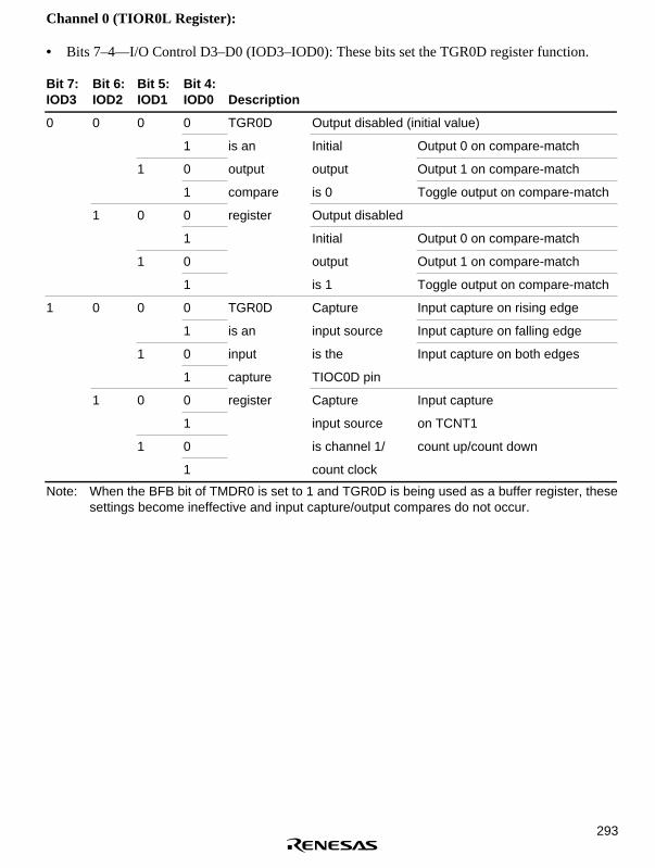
293
Channel 0 (TIOR0L Register):
• Bits 7–4—I/O Control D3–D0 (IOD3–IOD0): These bits set the TGR0D register function.
Bit 7:IOD3
Bit 6:IOD2
Bit 5:IOD1
Bit 4:IOD0 Description
0 0 0 0 TGR0D Output disabled (initial value)
1 is an Initial Output 0 on compare-match
1 0 output output Output 1 on compare-match
1 compare is 0 Toggle output on compare-match
1 0 0 register Output disabled
1 Initial Output 0 on compare-match
1 0 output Output 1 on compare-match
1 is 1 Toggle output on compare-match
1 0 0 0 TGR0D Capture Input capture on rising edge
1 is an input source Input capture on falling edge
1 0 input is the Input capture on both edges
1 capture TIOC0D pin
1 0 0 register Capture Input capture
1 input source on TCNT1
1 0 is channel 1/ count up/count down
1 count clock
Note: When the BFB bit of TMDR0 is set to 1 and TGR0D is being used as a buffer register, thesesettings become ineffective and input capture/output compares do not occur.

294
• Bits 3–0—I/O Control C3–C0 (IOC3–IOC0): These bits set the TGR0C register function.
Bit 3:IOC3
Bit 2:IOC2
Bit 1:IOC1
Bit 0:IOC0 Description
0 0 0 0 TGR0C Output disabled (initial value)
1 is an Initial Output 0 on compare-match
1 0 output output Output 1 on compare-match
1 compare is 0 Toggle output on compare-match
1 0 0 register Output disabled
1 Initial Output 0 on compare-match
1 0 output Output 1 on compare-match
1 is 1 Toggle output on compare-match
1 0 0 0 TGR0C Capture Input capture on rising edge
1 is an input source Input capture on falling edge
1 0 input is the Input capture on both edges
1 capture TIOC0C pin
1 0 0 register Capture Input capture
1 input source on TCNT1
1 0 is channel 1/ count up/count down
1 count clock
Note: When the BFA bit of TMDR0 is set to 1 and TGR0C is being used as a buffer register, thesesettings become ineffective and input capture/output compares do not occur.

295
Channel 1 (TIOR1 Register):
• Bits 7–4—I/O Control B3–B0 (IOB3–IOB0): These bits set the TGR1B register function.
Bit 7:IOB3
Bit 6:IOB2
Bit 5:IOB1
Bit 4:IOB0 Description
0 0 0 0 TGR1B Output disabled (initial value)
1 is an Initial Output 0 on compare-match
1 0 output output Output 1 on compare-match
1 compare is 0 Toggle output on compare-match
1 0 0 register Output disabled
1 Initial Output 0 on compare-match
1 0 output Output 1 on compare-match
1 is 1 Toggle output on compare-match
1 0 0 0 TGR1B Capture Input capture on rising edge
1 is an input source Input capture on falling edge
1 0 input is the Input capture on both edges
1 capture TIOC1B pin
1 0 0 register Capture input Input capture
1 source TGR0C on channel TGR0C
1 0 compare/match compare-match/input
1 input capture capture generation

296
• Bits 3–0—I/O Control A3–A0 (IOA3–IOA0): These bits set the TGR1A register function.
Bit 3:IOA3
Bit 2:IOA2
Bit 1:IOA1
Bit 0:IOA0 Description
0 0 0 0 TGR1A Output disabled (initial value)
1 is an Initial Output 0 on compare-match
1 0 output output Output 1 on compare-match
1 compare is 0 Toggle output on compare-match
1 0 0 register Output disabled
1 Initial Output 0 on compare-match
1 0 output Output 1 on compare-match
1 is 1 Toggle output on compare-match
1 0 0 0 TGR1A Capture Input capture on rising edge
1 is an input source Input capture on falling edge
1 0 input is the Input capture on both edges
1 capture TIOC1A pin
1 0 0 register Capture input Input capture
1 source is TGR0A on channel 0/TGR0A
1 0 compare-match/input
compare-match/input capturegeneration
1 capture

297
Channel 2 (TIOR2 Register):
• Bits 7–4—I/O Control B3–B0 (IOB3–IOB0): These bits set the TGR2B register function.
Bit 7:IOB3
Bit 6:IOB2
Bit 5:IOB1
Bit 4:IOB0 Description
0 0 0 0 TGR2B Output disabled (initial value)
1 is an Initial Output 0 on compare-match
1 0 output output Output 1 on compare-match
1 compare is 0 Toggle output on compare-match
1 0 0 register Output disabled
1 Initial Output 0 on compare-match
1 0 output Output 1 on compare-match
1 is 1 Toggle output on compare-match
1 0 0 0 TGR2B Capture Input capture on rising edge
1 is an input source Input capture on falling edge
1 0 input is the Input capture on both edges
1 capture TIOC2B pin
1 0 0 register Input capture on rising edge
1 Input capture on falling edge
1 0 Input capture on both edges
1

298
• Bits 3–0—I/O Control A3–A0 (IOA3–IOA0): These bits set the TGR2A register function.
Bit 3:IOA3
Bit 2:IOA2
Bit 1:IOA1
Bit 0:IOA0 Description
0 0 0 0 TGR2A Output disabled (initial value)
1 is an Initial Output 0 on compare-match
1 0 output output Output 1 on compare-match
1 compare is 0 Toggle output on compare-match
1 0 0 register Output disabled
1 Initial Output 0 on compare-match
1 0 output Output 1 on compare-match
1 is 1 Toggle output on compare-match
1 0 0 0 TGR2A Capture Input capture on rising edge
1 is an input source Input capture on falling edge
1 0 input is the Input capture on both edges
1 capture TIOC2A pin
1 0 0 register Input capture on rising edge
1 Input capture on falling edge
1 0 Input capture on both edges
1

299
Channel 3 (TIOR3H Register):
• Bits 7–4—I/O Control B3–B0 (IOB3–IOB0): These bits set the TGR3B register function.
Bit 7:IOB3
Bit 6:IOB2
Bit 5:IOB1
Bit 4:IOB0 Description
0 0 0 0 TGR3B Output disabled (initial value)
1 is an Initial Output 0 on compare-match
1 0 output output Output 1 on compare-match
1 compare is 0 Toggle output on compare-match
1 0 0 register Output disabled
1 Initial Output 0 on compare-match
1 0 output Output 1 on compare-match
1 is 1 Toggle output on compare-match
1 0 0 0 TGR3B Capture Input capture on rising edge
1 is an input source Input capture on falling edge
1 0 input is the Input capture on both edges
1 capture TIOC3B pin
1 0 0 register Input capture on rising edge
1 Input capture on falling edge
1 0 Input capture on both edges
1

300
• Bits 3–0—I/O Control A3–A0 (IOA3–IOA0): These bits set the TGR3A register function.
Bit 3:IOA3
Bit 2:IOA2
Bit 1:IOA1
Bit 0:IOA0 Description
0 0 0 0 TGR3A Output disabled (initial value)
1 is an Initial Output 0 on compare-match
1 0 output output Output 1 on compare-match
1 compare is 0 Toggle output on compare-match
1 0 0 register Output disabled
1 Initial Output 0 on compare-match
1 0 output Output 1 on compare-match
1 is 1 Toggle output on compare-match
1 0 0 0 TGR3A Capture Input capture on rising edge
1 is an input source Input capture on falling edge
1 0 input is the Input capture on both edges
1 capture TIOC3A pin
1 0 0 register Input capture on rising edge
1 Input capture on falling edge
1 0 Input capture on both edges
1

301
Channel 3 (TIOR3L Register):
• Bits 7–4—I/O Control D3–D0 (IOD3–IOD0): These bits set the TGR4D register function.
Bit 7:IOD3
Bit 6:IOD2
Bit 5:IOD1
Bit 4:IOD0 Description
0 0 0 0 TGR3D Output disabled (initial value)
1 is an Initial Output 0 on compare-match
1 0 output output Output 1 on compare-match
1 compare is 0 Toggle output on compare-match
1 0 0 register Output disabled
1 Initial Output 0 on compare-match
1 0 output Output 1 on compare-match
1 is 1 Toggle output on compare-match
1 0 0 0 TGR3D Capture Input capture on rising edge
1 is an input source Input capture on falling edge
1 0 input is the Input capture on both edges
1 capture TIOC3D pin
1 0 0 register Input capture on rising edge
1 Input capture on falling edge
1 0 Input capture on both edges
1
Note: When the BFB bit of TMDR3 is set to 1 and TGR3D is being used as a buffer register, thesesettings become ineffective and input capture/output compares do not occur.

302
• Bits 3–0—I/O Control C3–C0 (IOC3–IOC0): These bits set the TGR4C register function.
Bit 3:IOC3
Bit 2:IOC2
Bit 1:IOC1
Bit 0:IOC0 Description
0 0 0 0 TGR3C Output disabled (initial value)
1 is an Initial Output 0 on compare-match
1 0 output output Output 1 on compare-match
1 compare is 0 Toggle output on compare-match
1 0 0 register Output disabled
1 Initial Output 0 on compare-match
1 0 output Output 1 on compare-match
1 is 1 Toggle output on compare-match
1 0 0 0 TGR3C Capture Input capture on rising edge
1 is an input source Input capture on falling edge
1 0 input is the Input capture on both edges
1 capture TIOC3C pin
1 0 0 register Input capture on rising edge
1 Input capture on falling edge
1 0 Input capture on both edges
1
Note: When the BFA bit of TMDR3 is set to 1 and TGR3C is being used as a buffer register, thesesettings become ineffective and input capture/output compares do not occur.

303
Channel 4 (TIOR4H Register):
• Bits 7–4—I/O Control B3–B0 (IOB3–IOB0): These bits set the TGR4B register function.
Bit 7:IOB3
Bit 6:IOB2
Bit 5:IOB1
Bit 4:IOB0 Description
0 0 0 0 TGR4B Output disabled (initial value)
1 is an Initial Output 0 on compare-match
1 0 output output Output 1 on compare-match
1 compare is 0 Toggle output on compare-match
1 0 0 register Output disabled
1 Initial Output 0 on compare-match
1 0 output Output 1 on compare-match
1 is 1 Toggle output on compare-match
1 0 0 0 TGR4B Capture Input capture on rising edge
1 is an input source Input capture on falling edge
1 0 input is the Input capture on both edges
1 capture TIOC4B pin
1 0 0 register Input capture on rising edge
1 Input capture on falling edge
1 0 Input capture on both edges
1

304
• Bits 3–0—I/O Control A3–A0 (IOA3–IOA0): These bits set the TGR4A register function.
Bit 3:IOA3
Bit 2:IOA2
Bit 1:IOA1
Bit 0:IOA0 Description
0 0 0 0 TGR4A Output disabled (initial value)
1 is an Initial Output 0 on compare-match
1 0 output output Output 1 on compare-match
1 compare is 0 Toggle output on compare-match
1 0 0 register Output disabled
1 Initial Output 0 on compare-match
1 0 output Output 1 on compare-match
1 is 1 Toggle output on compare-match
1 0 0 0 TGR4A Capture Input capture on rising edge
1 is an input source Input capture on falling edge
1 0 input is the Input capture on both edges
1 capture TIOC4A pin
1 0 0 register Input capture on rising edge
1 Input capture on falling edge
1 0 Input capture on both edges
1

305
Channel 4 (TIOR4L Register):
• Bits 7–4—I/O Control D3–D0 (IOD3–IOD0): These bits set the TGR4D register function.
Bit 7:IOD3
Bit 6:IOD2
Bit 5:IOD1
Bit 4:IOD0 Description
0 0 0 0 TGR4D Output disabled (initial value)
1 is an Initial Output 0 on compare-match
1 0 output output Output 1 on compare-match
1 compare is 0 Toggle output on compare-match
1 0 0 register Output disabled
1 Initial Output 0 on compare-match
1 0 output Output 1 on compare-match
1 is 1 Toggle output on compare-match
1 0 0 0 TGR4D Capture Input capture on rising edge
1 is an input source Input capture on falling edge
1 0 input is the Input capture on both edges
1 capture TIOC4D pin
1 0 0 register Input capture on rising edge
1 Input capture on falling edge
1 0 Input capture on both edges
1
Note: When the BFB bit of TMDR4 is set to 1 and TGR4D is being used as a buffer register, thesesettings become ineffective and input capture/output compares do not occur.

306
• Bits 3–0—I/O Control C3–C0 (IOC3–IOC0): These bits set the TGR4C register function.
Bit 3:IOC3
Bit 2:IOC2
Bit 1:IOC1
Bit 0:IOC0 Description
0 0 0 0 TGR4C Output disabled (initial value)
1 is an Initial Output 0 on compare-match
1 0 output output Output 1 on compare-match
1 compare is 0 Toggle output on compare-match
1 0 0 register Output disabled
1 Initial Output 0 on compare-match
1 0 output Output 1 on compare-match
1 is 1 Toggle output on compare-match
1 0 0 0 TGR4C Capture Input capture on rising edge
1 is an input source Input capture on falling edge
1 0 input is the Input capture on both edges
1 capture TIOC4C pin
1 0 0 register Input capture on rising edge
1 Input capture on falling edge
1 0 Input capture on both edges
1
Note: When the BFA bit of TMDR4 is set to 1 and TGR4C is being used as a buffer register, thesesettings become ineffective and input capture/output compares do not occur.
12.2.4 Timer Interrupt Enable Register (TIER)
The TIER is an 8-bit register that controls the enable/disable of interrupt requests for each channel.The MTU has five TIER registers, one each for channel. TIER is initialized to H'40 by a reset orby standby mode.
Channel 0: TIER0:
Bit: 7 6 5 4 3 2 1 0
TTGE — — TCIEV TGIED TGIEC TGIEB TGIEA
Initial value: 0 1 0 0 0 0 0 0
R/W: R/W R R R/W R/W R/W R/W R/W

307
Channels 1, 2: TIER1, TIER2:
Bit: 7 6 5 4 3 2 1 0
TTGE — TCIEU TCIEV — — TGIEB TGIEA
Initial value: 0 1 0 0 0 0 0 0
R/W: R/W R R/W R/W R R R/W R/W
Channels 3, 4: TIER3, TIER4:
Bit: 7 6 5 4 3 2 1 0
TTGE — — TCIEV TGIED TGIEC TGIEB TGIEA
Initial value: 0 1 0 0 0 0 0 0
R/W: R/W R R R/W R/W R/W R/W R/W
• Bit 7—A/D Conversion Start Request Enable (TTGE): Enables or disables generation of anA/D conversion start request by a TGRA register input capture/compare-match.
Bit 7: TTGE Description
0 Disable A/D conversion start requests (initial value)
1 Enable A/D conversion start request generation
• Bit 6—Reserved: This bit is reserved. It always reads as 0, and cannot be modified.
• Bit 5—Underflow Interrupt Enable (TCIEU): Enables or disables interrupt requests when theunderflow flag (TCFU) of the channel 1, 2 timer status register (TSR) is set to 1.
This bit is reserved for channels 0, 3, and 4. It always reads as 0. The write value shouldalways be 1.
Bit 5: TCIEU Description
0 Disable UDF interrupt requests (TCIU) (initial value)
1 Enable UDF interrupt requests (TCIU)
• Bit 4—Overflow Interrupt Enable (TCIEV): Enables or disables interrupt requests when theoverflow flag TCFV of the timer status register (TSR) is set to 1.
Bit 4: TCIEV Description
0 Disable TCFV interrupt requests (TCIV) (initial value)
1 Enable TCFV interrupt requests (TCIV)

308
• Bit 3—TGR Interrupt Enable D (TGIED): Enables or disables interrupt TGFD requests whenthe TGFD bit of the channel 0, 3, 4 TSR register is set to 1.
This bit is reserved for channels 1 and 2. It always reads as 1. The write value should alwaysbe 1.
Bit 3: TGIED Description
0 Disable interrupt requests (TGID) due to the TGFD bit (initial value)
1 Enable interrupt requests (TGID) due to the TGFD bit
• Bit 2—TGR Interrupt Enable C (TGIEC): Enables or disables TGFC interrupt requests whenthe TGFC bit of the channel 0, 3, 4 TSR register is set to 1.
This bit is reserved for channels 1 and 2. It always reads as 1. The write value should alwaysbe 1.
Bit 2: TGIEC Description
0 Disable interrupt requests (TGIC) due to the TGFC bit (initial value)
1 Enable interrupt requests (TGIC) due to the TGFC bit
• Bit 1—TGR Interrupt Enable B (TGIEB): Enables or disables TGFB interrupt requests whenthe TGFB bit of the TSR register is set to 1.
Bit 1: TGIEB Description
0 Disable interrupt requests (TGIB) due to the TGFB bit (initial value)
1 Enable interrupt requests (TGIB) due to the TGFB bit
• Bit 0—TGR Interrupt Enable A (TGIEA): Enables or disables TGFA interrupt requests whenthe TGFA bit of the TSR register is set to 1.
Bit 0: TGIEA Description
0 Disable interrupt requests (TGIA) due to the TGFA bit (initial value)
1 Enable interrupt requests (TGIA) due to the TGFA bit

309
12.2.5 Timer Status Register (TSR)
The timer status register (TSR) is an 8-bit register that indicates the status of each channel. TheMTU has five TSR registers, one each for channel. TSR is initialized to H'C0 by a power-on resetor by standby mode. This register is not initialized by a manual reset.
Channel 0: TSR0:
Bit: 7 6 5 4 3 2 1 0
— — — TCFV TGFD TGFC TGFB TGFA
Initial value: 1 1 0 0 0 0 0 0
R/W: R R R R/(W)* R/(W)* R/(W)* R/(W)* R/(W)*
Note: * Only 0 writes to clear the flags are possible.
Channels 1, 2: TSR1, TSR2:
Bit: 7 6 5 4 3 2 1 0
TCFD — TCFU TCFV — — TGFB TGFA
Initial value: 1 1 0 0 0 0 0 0
R/W: R R R/(W)* R/(W)* R R R/(W)* R/(W)*
Note: * Only 0 writes to clear the flags are possible.
Channels 3, 4: TSR3, TSR4:
Bit: 7 6 5 4 3 2 1 0
TCFD — — TCFV TGFD TGFC TGFB TGFA
Initial value: 1 1 0 0 0 0 0 0
R/W: R R R R/(W)* R/(W)* R/(W)* R/(W)* R/(W)*
Note: * Only 0 writes to clear the flags are possible.
• Bit 7—Count Direction Flag (TCFD): This status flag indicates the count direction of thechannel 1, 2, 3, 4 TCNT counters.
This bit is reserved in channel 0. This bit always reads as 1. The write value should always be1.
Bit 7: TCFD Description
0 TCNT counts down
1 TCNT counts up (initial value)
• Bit 6—Reserved: This bit always reads as 1. The write value should always be 1.
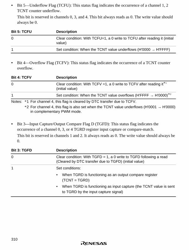
310
• Bit 5—Underflow Flag (TCFU): This status flag indicates the occurrence of a channel 1, 2TCNT counter underflow.
This bit is reserved in channels 0, 3, and 4. This bit always reads as 0. The write value shouldalways be 0.
Bit 5: TCFU Description
0 Clear condition: With TCFU=1, a 0 write to TCFU after reading it (initialvalue)
1 Set condition: When the TCNT value underflows (H'0000 → H'FFFF)
• Bit 4—Overflow Flag (TCFV): This status flag indicates the occurrence of a TCNT counteroverflow.
Bit 4: TCFV Description
0 Clear condition: With TCFV =1, a 0 write to TCFV after reading it* 1
(initial value)
1 Set condition: When the TCNT value overflows (H'FFFF → H'0000)* 2
Notes: * 1 For channel 4, this flag is cleared by DTC transfer due to TCFV.* 2 For channel 4, this flag is also set when the TCNT value underflows (H'0001 → H'0000)
in complementary PWM mode.
• Bit 3—Input Capture/Output Compare Flag D (TGFD): This status flag indicates theoccurrence of a channel 0, 3, or 4 TGRD register input capture or compare-match.
This bit is reserved in channels 1 and 2. It always reads as 0. The write value should always be0.
Bit 3: TGFD Description
0 Clear condition: With TGFD = 1, a 0 write to TGFD following a read(Cleared by DTC transfer due to TGFD) (initial value)
1 Set conditions:
• When TGRD is functioning as an output compare register(TCNT = TGRD)
• When TGRD is functioning as input capture (the TCNT value is sentto TGRD by the input capture signal)

311
• Bit 2—Input Capture/Output Compare Flag C (TGFC): This status flag indicates theoccurrence of a channel 0, 3, or 4 TGRC register input capture or compare-match.
This bit is reserved for channels 1 and 2. It always reads as 0. The write value should alwaysbe 0.
Bit 2: TGFC Description
0 Clear condition:
With TGFC = 1, a 0 write to TGFC following a read (Cleared by DTCtransfer due to TGFC) (initial value)
1 Set conditions:
• When TGRC is functioning as an output compare register(TCNT = TGRC)
• When TGRC is functioning as input capture (the TCNT value is sentto TGRC by the input capture signal)
• Bit 1—Input Capture/Output Compare Flag B (TGFB): This status flag indicates theoccurrence of a TGRB register input capture or compare-match.
Bit 1: TGFB Description
0 Clear condition: With TGFB = 1, a 0 write to TGFB following a read(Cleared by DTC transfer due to TGFB) (initial value)
1 Set conditions:
• When TGRB is functioning as an output compare register(TCNT = TGRB)
• When TGRB is functioning as input capture (the TCNT value is sentto TGRB by the input capture signal)
• Bit 0—Input Capture/Output Compare Flag A (TGFA): This status flag indicates theoccurrence of a TGRA register input capture or compare-match.
Bit 0: TGFA Description
0 Clear condition: With TGFA = 1, a 0 write to TGFA following a read(Cleared by DMAC transfer due to TGFA) (initial value)
1 Set conditions:
• When TGRA is functioning as an output compare register(TCNT = TGRA)
• When TGRA is functioning as input capture (the TCNT value is sentto TGRA by the input capture signal)

312
12.2.6 Timer Counters (TCNT)
The timer counters (TCNT) are 16-bit counters, with one for each channel, for a total of five.
The TCNT are initialized to H'0000 by a power-on reset and when in standby mode. Manual resetdoes not initialize TCNT. Accessing the TCNT counters in 8-bit units is prohibited. Always accessin 16-bit units.
Channel Abbreviation Function
0 TCNT0 Increment counter
1 TCNT1 Increment/decrement counter* 1
2 TCNT2 Increment/decrement counter* 1
3 TCNT3 Increment/decrement counter* 2
4 TCNT4 Increment/decrement counter* 2
Notes: * 1 Can only be used as an increment/decrement counter in phase counting mode, withother channel overflow/underflow counting. It becomes an increment counter in all othercases.
* 2 Can only be used as an increment counter in complementary PWM mode. It becomesan increment counter in all other cases.
Bit: 15 14 13 12 11 10 9 8
Initial value: 0 0 0 0 0 0 0 0
R/W: R/W R/W R/W R/W R/W R/W R/W R/W
Bit: 7 6 5 4 3 2 1 0
Initial value: 0 0 0 0 0 0 0 0
R/W: R/W R/W R/W R/W R/W R/W R/W R/W

313
12.2.7 Timer General Register (TGR)
Each timer general register (TGR) is a 16-bit register that can function as either an output compareregister or an input capture register. There are a total of sixteen TGR, four each for channels 0, 3,and 4, and two each for channels 1 and 2. The TGRC and TGRD of channels 0, 3, and 4 can be setto operate as buffer registers. The TGR register and buffer register combinations are TGRA withTGRC, and TGRB with TGRD.
The TGRs are initialized to H'FFFF by a power-on reset or in standby mode. Manual reset doesnot initialize TGR. Accessing of the TGRs in 8-bit units is disabled; they may only be accessed in16-bit units.
Bit: 15 14 13 12 11 10 9 8
Initial value: 1 1 1 1 1 1 1 1
R/W: R/W R/W R/W R/W R/W R/W R/W R/W
Bit: 7 6 5 4 3 2 1 0
Initial value: 1 1 1 1 1 1 1 1
R/W: R/W R/W R/W R/W R/W R/W R/W R/W
12.2.8 Timer Start Register (TSTR)
The timer start register (TSTR) is an 8-bit read/write register that starts and stops the timercounters (TCNT) of channels 0–4. TSTR is initialized to H'00 upon power-on reset or standbymode. Manual reset does not initialize TSTR.
Bit: 7 6 5 4 3 2 1 0
CST4 CST3 — — — CST2 CST1 CST0
Initial value: 0 0 0 0 0 0 0 0
R/W: R/W R/W R R R R/W R/W R/W
• Bits 7, 6, 2–0—Counter Start 4–0 (CST4–CST0): Select the start and stop of the timer counters(TCNT). The counter start to channel and bit to channel correspondence are indicated in thetables below.

314
Counter Start Channel
CST4 Channel 4 (TCNT4)
CST3 Channel 3 (TCNT3)
CST2 Channel 2 (TCNT2)
CST1 Channel 1 (TCNT1)
CST0 Channel 0 (TCNT0)
Bit n: CSTn Description
0 TCNTn count is halted (initial value)
1 TCNTn counts
Note: n = 4 to 0. However, CST4 is bit 7, CST3 is bit 6.If 0 is written to the CST bit during operation with the TIOC pin in output status, the counterstops, but the TIOC pin output compare output level is maintained. If a write is done to theTIOR register while the CST bit is a 0, the pin output level is updated to the establishedinitial output value. In complementary PWM mode or reset sync PWM mode, when a 0 iswritten to the CST bit of a TIOC pin in output mode during operation, it returns to the initialoutput.
• Bits 5–3—Reserved: These bits always read as 0. The write value should always be 0.
12.2.9 Timer Synchro Register (TSYR)
The timer synchro register (TSYR) is an 8-bit read/write register that selects independent orsynchronous TCNT counter operation for channels 0–4. Channels for which 1 is set in thecorresponding bit will be synchronized. TSYR is initialized to H'00 upon power-on reset orstandby mode. Manual reset does not initialize TSYR.
Bit: 7 6 5 4 3 2 1 0
SYNC4 SYNC3 — — — SYNC2 SYNC1 SYNC0
Initial value: 0 0 0 0 0 0 0 0
R/W: R/W R/W R R R R/W R/W R/W
• Bits 7, 6, 2–0—Timer Synchronization 4–0 (SYNC4–SYNC0): Selects operation independentof, or synchronized to, other channels. Synchronous operation allows synchronous clears dueto multiple TCNT synchronous presets and other channel counter clears. A minimum of twochannels must have SYNC bits set to 1 for synchronous operation. For synchronizationclearing, it is necessary to set the TCNT counter clear sources (the CCLR2–CCLR0 bits of theTCR register), in addition to the SYNC bit. The counter start to channel and bit-to-channelcorrespondence are indicated in the tables below.

315
Counter Start Channel
SYNC4 Channel 4 (TCNT4)
SYNC3 Channel 3 (TCNT3)
SYNC2 Channel 2 (TCNT2)
SYNC1 Channel 1 (TCNT1)
SYNC0 Channel 0 (TCNT0)
Bit n: SYNCn Description
0 Timer counter (TCNTn) independent operation (initial value)
(TCNTn preset/clear unrelated to other channels)
1 Timer counter synchronous operation* 1
TCNTn synchronous preset/ synchronous clear* 2 possible
Notes: n = 4 to 0. However, SYNC4 is bit 7, SYNC3 is bit 6.* 1 Minimum of two channel SYNC bits must be set to 1 for synchronous operation.* 2 TCNT counter clear sources (CCLR2–CCLR0 bits of the TCR register) must be set in
addition to the SYNC bit in order to have clear synchronization.
• Bits 5–3—Reserved: These bits always read as 0. The write value should always be 0.
12.2.10 Timer Output Master Enable Register (TOER)
The timer output master enable register (TOER) enables/disables output settings for output pinsTIOC4D, TIOC4C, TIOC3D, TIOC4B, TIOC4A, and TIOC3B. These pins do not output correctlyif the TOER bits have not been set. Set TOER of CH3 and CH2 prior to setting TIOR of CH3 andCH4. The TOER is an 8-bit read/write register. The register is initialized to H'C0 by a power-onreset or in standby mode. Manual reset does not initialize TOER.
Bit: 7 6 5 4 3 2 1 0
— — OE4D OE4C OE3D OE4B OE4A OE3B
Initial value: 1 1 0 0 0 0 0 0
R/W: R R R/W R/W R/W R/W R/W R/W
• Bits 7–6—Reserved: These bits always read as 1. The write value should always be 1.

316
• Bit 5—Master Enable TIOC4D (OE4D): Enables or disables the TIOC4D pin MTU output.
Bit 5: OE4D Description
0 Disable TIOC4D pin MTU output (initial value)
1 Enable TIOC4D pin MTU output
• Bit 4—Master Enable TIOC4C (OE4C): Enables or disables the TIOC4C pin MTU output.
Bit 4: OE4C Description
0 Disable TIOC4C pin MTU output (initial value)
1 Enable TIOC4C pin MTU output
• Bit 3—Master Enable TIOC3D (OE3D): Enables or disables the TIOC3D pin MTU output.
Bit 3: OE3D Description
0 Disable TIOC3D pin MTU output (initial value)
1 Enable TIOC3D pin MTU output
• Bit 2—Master Enable TIOC4B (OE4B): Enables or disables the TIOC4B pin MTU output.
Bit 2: OE4B Description
0 Disable TIOC4B pin MTU output (initial value)
1 Enable TIOC4B pin MTU output
• Bit 1—Master Enable TIOC4A (OE4A): Enables or disables the TIOC4A pin MTU output.
Bit 1: OE4A Description
0 Disable TIOC4A pin MTU output (initial value)
1 Enable TIOC4A pin MTU output
• Bit 0—Master Enable TIOC3B (OE3B): Enables or disables the TIOC3B pin MTU output.
Bit 0: OE3B Description
0 Disable TIOC3B pin MTU output (initial value)
1 Enable TIOC3B pin MTU output

317
12.2.11 Timer Output Control Register (TOCR)
The timer output control register (TOCR) enables/disables PWM synchronized toggle output incomplementary PWM mode and reset sync PWM mode, and controls output level inversion ofPWM output. The TOCR is initialized to H'00 by a power-on reset or in the standby mode.Manual reset does not initialize TOCR. These register settings are ineffective for anything otherthan complementary PWM mode/reset-synchronized PWM mode.
Bit: 7 6 5 4 3 2 1 0
— PSYE — — — — OLSN OLSP
Initial value: 0 0 0 0 0 0 0 0
R/W: R R/W R R R R R/W R/W
• Bits 7, 5–2—Reserved: These bits always read as 1. The write value should always be 1.
• Bit 6—PWM Synchronous Output Enable (PSYE): Selects the enable/disable of toggle outputsynchronized with the PWM period.
Bit 6: PSYE Description
0 Toggle output synchronous with PWM period disabled (initial value)
1 Toggle output synchronous with PWM period enabled
• Bit 1—Output Level Select N (OLSN): Selects the reverse phase output level of thecomplementary PWM mode or reset-synchronized PWM mode.
Compare Match Output
OLSN Initial Output Active Level Increment Count Decrement Count
0 High level* Low level High level Low level (initialvalue)
1 Low level* High level Low level High level
Note: * The reverse phase waveform initial output value changes to active level after elapse of thedead time after count start.
• Bit 0—Output Level Select P (OLSP): Selects the positive phase output level of thecomplementary PWM mode or reset-synchronized PWM mode.
Compare Match Output
OLSP Initial Output Active Level Increment Count Decrement Count
0 High level Low level Low level High level (initial value)
1 Low level High level High level Low level

318
Figure 12.2 shows an example of complementary PWM mode output (1 phase) when OLSN = 1,OLSP = 1.
TCNT3 andTCNT4 values
TGR3A
TGR4A
H'0000
Positivephase output
Reversephase output
TDDR
TCNT4
TCNT3
Time
Activelevel
Initialoutput
Initialoutput
Compare matchoutput (up count)
Compare matchoutput (up count)
Compare matchoutput (down count)
Compare matchoutput (down count)
Active level
Active level
Figure 12.2 Complementary PWM Mode Output Level Example
12.2.12 Timer Gate Control Register (TGCR)
The timer gate control register (TGCR) is an 8-bit read/write register that controls the waveformoutput necessary for brushless DC motor control in complementary PWM mode/reset-synchronized PWM mode. The TGCR is initialized to H'80 by a power-on reset or in the standbymode. Manual reset does not initialize TGCR. These register settings are ineffective for anythingother than complementary PWM mode/reset-synchronized PWM mode.
Bit: 7 6 5 4 3 2 1 0
— BDC N P FB WF VF UF
Initial value: 1 0 0 0 0 0 0 0
R/W: R R/W R/W R/W R/W R/W R/W R/W
• Bit 7—Reserved: This bit always reads as 1. The write value should always be 1.

319
• Bit 6—Brushless DC Motor (BDC): Selects gate signal output/chopping output function forbrushless DC motor control.
Bit 6: BDC Description
0 Ordinary output (initial value)
1 Gate signal/chopping output for brushless DC motor
• Bit 5—Reverse Phase Output (N): Selects whether to output gate signals directly to the reversephase pin (TIOC3D, TIOC4C, and TIOC4D) output, or to output by chopping the gate signaland the complementary PWM/reset-synchronized PWM output.
Bit 5: N Description
0 Output gate signals directly to reverse phase pin output (initial value)
1 Output chopped gate signal and complementary PWM /reset-synchronized PWM output to reverse phase pin output
• Bit 4—Positive Phase Output (P): Selects whether to output gate signals directly to the positivephase pin (TIOC3B, TIOC4A, and TIOC4B) output, or to output by chopping the gate signaland the complementary PWM/reset-synchronized PWM output.
Bit 4: P Description
0 Output gate signals directly to positive phase pin output (initial value)
1 Output chopped gate signal and complementary PWM /reset-synchronized PWM output to positive phase pin output
• Bit 3—Feedback Input (FB): Selects whether to use external input or register input for thefeedback input to generate gate signals.
Bit 3: FB Description
0 Feedback input is external input (initial value)(Input sources are channel 0 TGRA, TGRB, TGRC input capture signals)
1 Feedback input is register input (TGCR’s UF, VF, WF settings)

320
• Bits 2–0—Output Phase Switch 2–0 (WF, VF, UF): These bits set the positive phase/negativephase output phase on or off state. The setting of these bits is valid only when the FB bit in thisregister is set to 1. In this case, the setting of bits 2–0 is a substitute for external input.
Function
TIOC3B TIOC4A TIOC4B TIOC3D TIOC4C TIOC4D
Bit 2:WF
Bit 1:VF
Bit 0:UF
UPhase
VPhase
WPhase
UPhase
VPhase
WPhase
0 0 0 Off Off Off Off Off Off Initial value
1 On Off Off Off Off On —
1 0 Off On Off On Off Off —
1 Off On Off Off Off On —
1 0 0 Off Off On Off On Off —
1 On Off Off Off On Off —
1 0 Off Off On On Off Off —
1 Off Off Off Off Off Off —
12.2.13 Timer Subcounter (TCNTS)
The timer subcounter (TCNTS) is a 16-bit read-only counter that is used only in complementaryPWM mode. The TCNTS counter is initialized to H'00 by a power-on reset or in standby mode.Manual reset does not initialize TCNTS. Accessing the TCNTS counter in 8-bit units isprohibited. Always access in 16-bit units.
Bit: 15 14 13 12 11 10 9 8
Initial value: 0 0 0 0 0 0 0 0
R/W: R R R R R R R R
Bit: 7 6 5 4 3 2 1 0
Initial value: 0 0 0 0 0 0 0 0
R/W: R R R R R R R R

321
12.2.14 Timer Dead Time Data Register (TDDR)
The timer dead time data register (TDDR) is a 16-bit register, used only in complementary PWMmode, that specifies the TCNT3 and TCNT4 counter offset values. In complementary PWM mode,when the TCNT3 and TCNT4 counters are cleared and then restarted, the TDDR register value isloaded into the TCNT3 counter and the count operation starts. The TDDR register is initialized toH'FFFF by a power-on reset or in standby mode. Manual reset does not initialize TDDR.Accessing the TDDR in 8-bit units is prohibited. Always access in 16-bit units.
Bit: 15 14 13 12 11 10 9 8
Initial value: 1 1 1 1 1 1 1 1
R/W: R/W R/W R/W R/W R/W R/W R/W R/W
Bit: 7 6 5 4 3 2 1 0
Initial value: 1 1 1 1 1 1 1 1
R/W: R/W R/W R/W R/W R/W R/W R/W R/W
12.2.15 Timer Period Data Register (TCDR)
The timer period data register (TCDR) is a 16-bit register used only in complementary PWMmode. Set the PWM carrier sync value as the TCDR register value. This register is constantlycompared with the TCNTS counter in complementary PWM mode, and when a match occurs theTCNTS counter switches direction (decrement to increment).
The TCDR register is initialized to H'FFFF by a reset or in standby mode. Manual reset does notinitialize TCDR. Accessing the TCDR in 8-bit units is prohibited. Always access in 16-bit units.
Bit: 15 14 13 12 11 10 9 8
Initial value: 1 1 1 1 1 1 1 1
R/W: R/W R/W R/W R/W R/W R/W R/W R/W
Bit: 7 6 5 4 3 2 1 0
Initial value: 1 1 1 1 1 1 1 1
R/W: R/W R/W R/W R/W R/W R/W R/W R/W

322
12.2.16 Timer Period Buffer Register (TCBR)
The timer period buffer register (TCBR) is a 16-bit register used only in complementary PWMmode. It functions as a buffer register for the TCDR register. The TCBR register values aretransferred to the TCDR register with the transfer timing established in the TMDR register. TheTCBR register is initialized to H'FFFF by a power-on reset or in standby mode. Manual reset doesnot initialize TCBR. Accessing the TCBR in 8-bit units is prohibited. Always access in 16-bitunits.
Bit: 15 14 13 12 11 10 9 8
Initial value: 1 1 1 1 1 1 1 1
R/W: R/W R/W R/W R/W R/W R/W R/W R/W
Bit: 7 6 5 4 3 2 1 0
Initial value: 1 1 1 1 1 1 1 1
R/W: R/W R/W R/W R/W R/W R/W R/W R/W
12.3 Bus Master Interface
12.3.1 16-Bit Registers
The timer counters (TCNT) and general registers (TGR) are 16-bit registers. A 16-bit data bus tothe bus master enables 16-bit read/writes. 8-bit read/write is not possible. Always access in 16-bitunits. Figure 12.3 shows an example of 16-bit register access operation.
TCNTH TCNTL
Businterface
Upper 8 bits
Lower 8 bits
Bus master
Internal data busModule data bus
Figure 12.3 16-Bit Register Access Operation (Bus Master ↔ TCNT (16 Bit))

323
12.3.2 8-Bit Registers
All registers other than the TCNT and general registers (TGR) are 8-bit registers. These areconnected to the CPU by a 16-bit data bus, so 16-bit read/writes and as 8-bit read/writes are bothpossible (figures 12.4 ,12.5, and 12.6).
TCR
Businterface
Upper 8 bits
Lower 8 bits
Bus master
Internal data busModule data bus
Figure 12.4 8-Bit Register Access Operation (Bus Master ↔ TCR (Upper 8 Bits))
TMDR
Businterface
Upper 8 bits
Lower 8 bits
Bus master
Internal data busModule data bus
Figure 12.5 8-Bit Register Access Operation (Bus Master ↔ TMDR (Lower 8 Bits))
TCR TMDR
Businterface
Upper 8 bits
Lower 8 bits
Bus master
Internal data busModule data bus
Figure 12.6 8-Bit Register Access Operation (Bus Master ↔ TCR, TMDR (16 Bit))

324
12.4 Operation
12.4.1 Overview
The operation modes are described below.
Ordinary Operation: Each channel has a timer counter (TCNT) and general register (TGR). TheTCNT is an upcounter and can also operate as a free-running counter, periodic counter or externalevent counter. General registers (TGR) can be used as output compare registers or input captureregisters.
Synchronized Operation: The TCNT of a channel set for synchronized operation does asynchronized preset. When any TCNT of a channel operating in the synchronized mode isrewritten, the TCNTs of other channels are simultaneously rewritten as well. The timersynchronization bits of the TSYR registers of multiple channels set for synchronous operation canbe set to clear the TCNTs simultaneously.
Buffer Operation: When TGR is an output compare register, the buffer register value of thecorresponding channel is transferred to the TGR when a compare-match occurs. When TGR is aninput capture register, the TCNT counter value is transferred to the TGR when an input captureoccur simultaneously the value previously stored in the TGR is transferred to the buffer register.
Cascade Connection Operation: The channel 1 and channel 2 counters (TCNT1 and TCNT2)can be connected together to operate as a 32-bit counter.
PWM Mode: In PWM mode, a PWM waveform is output. The output level can be set by theTIOR register. Each TGR can be set for PWM waveform output with a duty cycle between 0%and 100%.
Phase Counting Mode: In phase counting mode, the phase differential between two clocks inputfrom the channel 1 and channel 2 external clock input pins is detected and the TCNT counteroperates as an up/down counter. In phase counting mode, the corresponding TCLK pins becomeclock inputs and TCNT functions as an up/down counter. It can be used as a two-phase encoderpulse input.
Reset-Synchronized PWM Mode: Three-phase positive and negative PWM waveforms can beobtained using channels 3 and 4 (the three phases of the PWM waveform share a transition pointon one side). When set for reset-synchronized PWM mode, TGR3A, TGR3B, TGR4A, andTGR4B automatically become output compare registers. The TIOC3A, TIOC3B, TIOC4A,TIOC4B, TIOC4C, and TIOC4D pins also become PWM output pins, and TCNT3 and TCNT4become upcounters. TCNT4, TGR4A, and TGR4B are isolated from TCNT4.

325
Complementary PWM Mode: Three-phase complementary positive and negative PWMwaveforms whose positive and negative phases do not overlap can be obtained using channels 3and 4. When set for complementary PWM mode, TGR3A, TGR3B, TGR4A, and TGR4B becomeoutput compare registers. The TIOC3B, TIOC3D, TIOC4A, TIOC4B, TIOC4C, and TIOC4D pinsalso automatically become PWM output pins while TCNT3 and TCNT4 become up/downcounters.
12.4.2 Basic Functions
Always select MTU external pin set function using the pin function controller (PFC).
Counter Operation: When a start bit (CST0–CST4) in the timer start register (TSTR) is set to 1,the corresponding timer counter (TCNT) starts counting. There are two counting modes: a free-running mode and a periodic mode.
To select the counting operation (figure 12.7):
1. Set bits TPSC2–TPSC0 in the TCR to select the counter clock. At the same time, set bitsCKEG1 and CKEG0 in the TCR to select the desired edge of the input clock.
2. To operate as a periodic counter, set the CCLR2–CCLR0 bits in the TCR to select TGR as aclearing source for the TCNT.
3. Set the TGR selected in step 2 as an output compare register using the timer I/O controlregister (TIOR).
4. Write the desired cycle value in the TGR selected in step 2.
5. Set the CST bit in the TSTR to 1 to start counting.
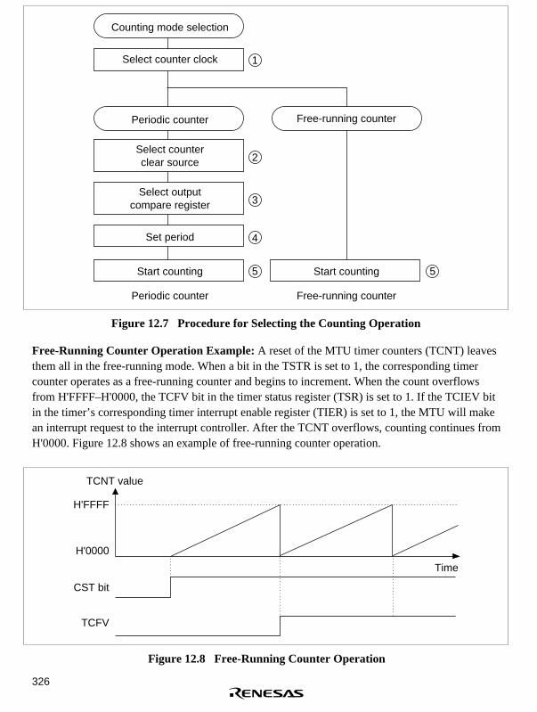
326
Counting mode selection
Select counter clock
Periodic counter
Select counterclear source
Select outputcompare register
Set period
Start counting Start counting
Free-running counter
Periodic counter Free-running counter
55
4
3
2
1
Figure 12.7 Procedure for Selecting the Counting Operation
Free-Running Counter Operation Example: A reset of the MTU timer counters (TCNT) leavesthem all in the free-running mode. When a bit in the TSTR is set to 1, the corresponding timercounter operates as a free-running counter and begins to increment. When the count overflowsfrom H'FFFF–H'0000, the TCFV bit in the timer status register (TSR) is set to 1. If the TCIEV bitin the timer’s corresponding timer interrupt enable register (TIER) is set to 1, the MTU will makean interrupt request to the interrupt controller. After the TCNT overflows, counting continues fromH'0000. Figure 12.8 shows an example of free-running counter operation.
CST bit
TCNT value
Time
H'FFFF
H'0000
TCFV
Figure 12.8 Free-Running Counter Operation

327
Periodic Counter Operation Example: Periodic counter operation is obtained for a givenchannel’s TCNT by selecting compare-match as a TCNT clear source. Set the TGR register forperiod setting to output compare register and select counter clear upon compare-match using theCCLR2–CCLR0 bits of the timer control register (TCR). After these settings, the TCNT beginsincrementing as a periodic counter when the corresponding bit of TSTR is set to 1. When thecount matches the TGR register value, the TGF bit in the TSR is set to 1 and the counter is clearedto H'0000. If the TGIE bit of the corresponding TIER is set to 1 at this point, the MTU will makean interrupt request to the interrupt controller. After the compare-match, TCNT continues countingfrom H'0000. Figure 12.9 shows an example of periodic counting.
CST bit
TCNT value
Time
Counter cleared byTGR compare match
TGR
H'0000
TGF
Flag cleared by softwareor DTC/DMAC activation
Figure 12.9 Periodic Counter Operation
Compare-Match Waveform Output Function: The MTU can output 0 level, 1 level, or toggleoutput from the corresponding output pins upon compare-matches.
Procedure for selecting the compare-match waveform output operation (figure 12.10):
1. Set the TIOR to select 0 output or 1 output for the initial value, and 0 output, 1 output, ortoggle output for compare-match output. The TIOC pin will output the set initial value until thefirst compare-match occurs.
2. Set a value in the TGR to select the compare-match timing.
3. Set the CST bit in the TSTR to 1 to start counting.
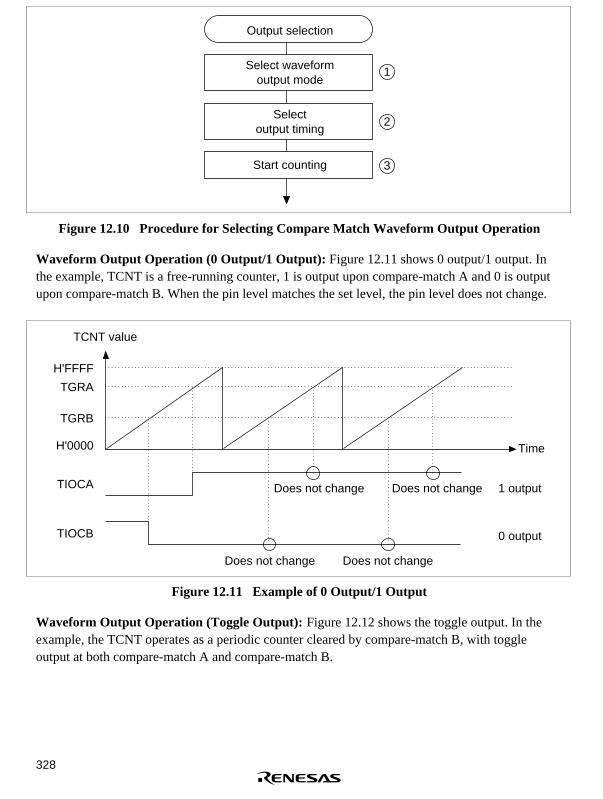
328
Output selection
Select waveformoutput mode
Selectoutput timing
Start counting
1
2
3
Figure 12.10 Procedure for Selecting Compare Match Waveform Output Operation
Waveform Output Operation (0 Output/1 Output): Figure 12.11 shows 0 output/1 output. Inthe example, TCNT is a free-running counter, 1 is output upon compare-match A and 0 is outputupon compare-match B. When the pin level matches the set level, the pin level does not change.
H'FFFF
H'0000
TIOCA
TCNT value
Time
TGRA
TGRB
TIOCB
Does not change Does not change 1 output
Does not change Does not change
0 output
Figure 12.11 Example of 0 Output/1 Output
Waveform Output Operation (Toggle Output): Figure 12.12 shows the toggle output. In theexample, the TCNT operates as a periodic counter cleared by compare-match B, with toggleoutput at both compare-match A and compare-match B.

329
H'FFFF
H'0000
TIOCA
TCNT valueCounter cleared by TGRB compare match
Time
TGRB
TGRA
TIOCB
Toggleoutput
Toggleoutput
Figure 12.12 Example of Toggle Output
Input Capture Function: In the input capture mode, the TCNT value is transferred into the TGRregister when the input edge is detected at the input capture/output compare pin (TIOC).
Detection can take place on the rising edge, falling edge, or both edges. Channels 0 and 1 can useother channel counter input clocks or compare-match signals as input capture sources.
The procedure for selecting the input capture operation (figure 12.13) is:
1. Set the TIOR to select the input capture function of the TGR, then select the input capturesource, and rising edge, falling edge, or both edges as the input edge.
2. Set the CST bit in the TSTR to 1 to start the TCNT counting.
Input selection
Select input-capture input
Start counting
Input capture operation
1
2
Figure 12.13 Procedure for Selecting Input Capture Operation

330
Input Capture Operation: Figure 12.14 shows input capture. The falling edge of TIOCB andboth edges of TIOCA are selected as input capture input edges. In the example, TCNT is set toclear at the input capture of the TGRB register.
Counter cleared by TIOCB input (falling edge)
TCNT value
H'0180H'0160
H'0005H'0010
H'0000
TIOCB
TIOCA
TGRA
TGRB
H'0005 H'0160 H'0010
H'0180
Time
Figure 12.14 Input Capture Operation
12.4.3 Synchronous Operation
In the synchronizing mode, two or more timer counters can be rewritten simultaneously(synchronized preset). Multiple timer counters can also be cleared simultaneously using TCRsettings (synchronized clear).
The synchronizing mode can increase the number of TGR registers for a single time base. All fivechannels can be set for synchronous operation.

331
Procedure for Selecting the Synchronizing Mode (Figure 12.15):
1. Set 1 in the SYNC bit of the timer synchro register (TSYR) to use the corresponding channelin the synchronizing mode.
2. When a value is written in the TCNT in any of the synchronized channels, the same value issimultaneously written in the TCNT in the other channels.
3. Set the counter to clear with output compare/input capture using bits CCLR2–CCLR0 in theTCR.
4. Set the counter clear source to synchronized clear using the CCLR2–CCLR0 bits of the TCR.
5. Set the CST bits for the corresponding channels in the TSTR to 1 to start counting in theTCNT.
Select counterclear source
Channel thatgenerated clear
source?
No
Yes
Selectsynchronizing mode
Set synchronizingmode
Synchronized preset
Set TCNT
Start counting
Set countersynchronous clear
Start counting
Counter clear Synchronized clearSynchronized preset
Synchronized clear
1
2
3
5
4
5
Figure 12.15 Procedure for Selecting Synchronizing Operation

332
Synchronized Operation: Figure 12.16 shows an example of synchronized operation. Channels0, 1, and 2 are set to synchronized operation and PWM mode 1. Channel 0 is set for a counterclear upon compare-match with TGR0B. Channels 1 and 2 are set for synchronous counter clearsby synchronous presets and TGR0B register compare-matches. Accordingly, a three-phase PWMwaveform with the data set in the TGR0B register as its PWM period is output from the TIOC0A,TIOC1A, and TIOC2A pins.
See section 12.4.6, PWM Mode, for details on the PWM mode.
TCNT0–TCNT2values
Time
TIOC0A
Synchronized clear on TGR0B compare match
TGR0B
TGR1B
TGR0A
TGR2B
TGR1A
TGR2A
H'0000
TIOC1A
TIOC2A
Figure 12.16 Synchronized Operation Example

333
12.4.4 Buffer Operation
Buffer operation is a function of channels 0, 3, and 4. TGRC and TGRD can be used as bufferregisters. Table 12.5 shows the register combinations for buffer operation.
Table 12.5 Register Combinations
Channel General Register Buffer Register
0 TGR0A TGR0C
TGR0B TGR0D
3 TGR3A TGR3C
TGR3B TGR3D
4 TGR4A TGR4C
TGR4B TGR4D
The buffer operation differs, depending on whether the TGR has been set as an input captureregister or an output compare register.
When TGR Is an Output Compare Register: When a compare-match occurs, the correspondingchannel buffer register value is transferred to the general register. Figure 12.17 shows an example.
Compare match signal
Bufferregister
TCNTComparatorGeneralregister
Figure 12.17 Compare Match Buffer Operation
When TGR Is an Input Capture Register: When an input capture occurs, the timer counter(TCNT) value is transferred to the general register (TGR), and the value that had been held up tothat time in the TGR is transferred to the buffer register (figure 12.18).
Input capture signal
TCNTBuffer
registerGeneralregister
Figure 12.18 Input Capture Buffer Operation

334
Procedure for Setting Buffer Mode (Figure 12.19):
1. Use the timer I/O control register (TIOR) to set the TGR as either an input capture or outputcompare register.
2. Use the timer mode register (TMDR) BFA, and BFB bits to set the TGR for buffer mode.
3. Set the CST bit in the TSTR to 1 to start the count operation.
1
2
3
Select TGR function
Buffer mode
Select buffer mode
Start counting
Buffer mode
Figure 12.19 Buffer Operation Setting Procedure
Buffer Operation Examples—when TGR Is an Output Compare Register: Figure 12.20shows an example of channel 0 set to PWM mode 1, and the TGRA and TGRC registers set forbuffer operation.
The TCNT counter is cleared by a compare-match B, and the output is a 1 upon compare-match Aand 0 output upon compare-match B. Because buffer mode is selected, a compare-match Achanges the output, and the buffer register TGRC value is simultaneously transferred to thegeneral register TGRA. This operation is repeated with each occurrence of a compare-match A.
See section 12.4.6, PWM Mode, for details on the PWM mode.

335
TGR0B
TGR0A
H'0000
TGR0C
TGR0A
TIOC0A
H'0450 H'0520
H'0200
H'0450 H'0520
H'0200
TCNT value
Time
Transfer
H'0450
H'0200
Figure 12.20 Buffer Operation Example (Output Compare Register)
Buffer Operation Examples—when TGR Is an Input Capture Register: Figure 12.21 showsan example of TGRA set as an input capture register with the TGRA and TGRB registers set forbuffer operation.
The TCNT counter is cleared by a TGRA register input capture, and the TIOCA pin input captureinput edge is selected as both rising and falling edge. Because buffer mode is selected, an inputcapture A causes the TCNT counter value to be stored in the TGRA register, and the value thatwas stored in the TGRA up until that time is simultaneously transferred to the TGRC register.
H'0F07
H'09FB
H'0532
H'0000
TGRA
TGRC
TIOCA
H'0532 H'09FBH'0F07
TCNT value
Time
H'0F07H'0532
Figure 12.21 Buffer Operation Example (Input Capture Register)

336
12.4.5 Cascade Connection Mode
Cascade connection mode is a function that connects the 16-bit counters of two channels togetherto act as a 32-bit counter.
This function operates by using the TPSC2–TPSC0 bits of the TCR register to set the channel 1counter clock to count by TCNT2 counter overflow/underflow.
Note: When channel 1 is set to phase counting mode, the counter clock settings becomeineffective.
Table 12.6 shows the cascade connection combinations.
Table 12.6 Cascade Connection Combinations
Combination Upper 16 Bits Lower 16 Bits
Channel 1, channel 2 TCNT1 TCNT2
Procedure for Setting Cascade Connection Mode (Figure 12.22):
1. Set the TPSC2–TPSC 0 bits of the channel 1 timer control register (TCR) to B'111 to select“count by TCNT2 overflow/underflow.”
2. Set the CST bits corresponding to the upper and lower 16 bits in the TSTR to 1 to start thecount operation.
Cascade connection operation
Select cascade connection
Start counting
Cascade connection operation
1
2
Figure 12.22 Procedure for Selecting Cascade Connection Mode

337
Cascade Connection Operation Examples—Phase Counting Mode: Figure 12.23 shows anexample of operation when the TCNT1 counter is set to count on TCNT2 overflow/underflow andchannel 2 is set to phase counting mode.
The TCNT1 counter increments with a TCNT2 counter overflow and decrements with a TCNT2underflow.
TCLKC
TCLKD
TCNT2 FFFD FFFF FFFFFFFE 0000 0001 0001 00000002
TCNT1 0000 00000001
Figure 12.23 Cascade Connection Operation Example (Phase Counting Mode)
12.4.6 PWM Mode
PWM mode outputs the various PWM waveforms from output pins. Output levels of 0 output, 1output, or toggle output can be selected as the output level for the compare-match of each TGR.
A period can be set for a register by using the TGR compare-match as a counter clear source. Allfive channels can be independently set to PWM mode. Synchronous operation is also possible.
There are two PWM modes:
• PWM mode 1
Generates PWM output using the TGRA and TGRB registers, and TGRC and TGRD registersas pairs. The initial output values are those established in the TGRA and TGRC registers.When the values set in TGR registers being used as a pair are equal, output values will notchange even if a compare-match occurs.
A maximum of 8-phase PWM output is possible for PWM mode 1.
• PWM mode 2
Generates PWM output using one TGR register as a period register and another as a duty cycleregister. The output value of each pin upon a counter clear is the initial value established by theTIOR register. When the values set in the period register and duty register are equal, outputvalues will not change even if a compare-match occurs. PWM mode 2 can be set only forchannels 0, 1, and 2.

338
Table 12.7 lists the combinations of PWM output pins and registers.
Table 12.7 Combinations of PWM Output Pins and Registers
Output Pin
Channel Register PWM Mode 1 PWM Mode 2
0 (AB pair) TGR0ATGR0B
TIOC0A TIOC 0ATIOC 0B
0 (CD pair) TGR0CTGR0D
TIOC0C TIOC 0CTIOC 0D
1 TGR1ATGR1B
TIOC1A TIOC 1ATIOC 1B
2 TGR2ATGR2B
TIOC2A TIOC 2ATIOC 2B
3 (AB pair) TGR3ATGR3B
TIOC3A Setting not possible
3 (CD pair) TGR3CTGR3D
TIOC3C
4 (AB pair) TGR4ATGR4B
TIOC4A
4 (CD pair) TGR4CTGR4D
TIOC4C
Note: PWM output of the period setting TGR is not possible in PWM mode 2.
Procedure for Selecting the PWM Mode (Figure 12.24):
1. Set bits TPSC2–TPSC0 in the TCR to select the counter clock source. At the same time, setbits CKEG1 and CKEG0 in the TCR to select the desired edge of the input clock.
2. Set bits CCLR2–CCLR0 in the TCR to select the TGR to be used as a counter clear source.
3. Set the period in the TGR selected in step 2, and the duty cycle in another TGR.
4. Using the timer I/O control register (TIOR), set the TGR selected in step 3 to act as an outputcompare register, and select the initial value and output value.
5. Set the MD3–MD 0 bits in TMDR to select the PWM mode.
6. Set the CST bit in the TSTR to 1 to let the TCNT start counting.

339
1
2
3
4
5
6
PWM mode
Select counter clock
Select waveform output level
Set TGR
Select PWM mode
Start counting
PWM mode
Select counter clear source
Figure 12.24 Procedure for Selecting the PWM Mode
PWM Mode Operation Examples—PWM Mode 1 (Figure 12.25): A TGRA register compare-match is used as a TCNT counter clear source, the TGRA register initial output value and outputcompare output value are both 0, and the TGRB register output compare output value is a 1. In thisexample, the value established in the TGRA register becomes the period and the value establishedin the TGRB register becomes the duty cycle.
Counter cleared by TGRA compare match
TCNT value
TGRA
TGRB
H'0000
TIOCA
Time
Figure 12.25 PWM Mode Operation Example (Mode 1)

340
PWM Mode Operation Examples—PWM Mode 2 (Figure 12.26): Channels 0 and 1 are set forsynchronous operation, TGR1B register compare-match is used as a TCNT counter clear source,the other TGR register initial output value is 0 and output compare output value is 1, and a 5-phasePWM waveform is output. In this example, the value established in the TGR1B register becomesthe period and the value established in the other TGR register becomes the duty cycle.
TGR0ATGR0BTGR0CTGR0DTGR1ATGR1B
TCNT value
TimeH'0000
TIOC0A
TIOC0B
TIOC0C
TIOC0D
TIOC1A
Counter cleared on TGR1B compare match
Figure 12.26 PWM Mode Operation Example (Mode 2)
0% Duty Cycle: Figure 12.27 shows an example of a 0% duty cycle PWM waveform output inPWM mode.
TGRA
TCNT valueTGRB rewrite
TGRB
TIOCA
Time
0% duty cycle
TGRB rewrite TGRB rewrite
Figure 12.27 PWM Mode Operation Example (0% Duty Cycle)

341
100% Duty Cycle: Figure 12.28 shows an example of a 100% duty cycle PWM waveform outputin PWM mode.
In PWM mode, when setting cycle = duty cycle the output waveform does not change, nor is therea change of waveform for the first pulse immediately after clearing the counter.
TGRA
TCNT value
TGRB rewrite
TGRB
TIOCA
TIOCA
Time
Time
100% duty cycle
Output does not change if period register and dutycycle register compare matches occur simultaneously
Output does not change if period register and dutycycle register compare matches occur simultaneously
TGRB rewrite
TGRB rewrite
TGRA
TCNT value
TGRB rewrite
TGRB
TGRB rewrite
100% duty cycle 0% duty cycle
TGRB rewrite
Figure 12.28 PWM Mode Operation Example (100% Duty Cycle)
12.4.7 Phase Counting Mode
The phase counting mode detects the phase differential of two external clock inputs and counts theTCNT counter up or down. This mode can be set for channels 1 and 2.
When set in the phase counting mode, an external clock is selected for the counter input clock,regardless of the settings of the TPSC2–TPSC0 bits of TCR or the CKEG1 and CKEG0 bits.TCNT also becomes an up/down counter. Since the TCR CCLR1/CCLR0 bits, TIOR, TIER, andTGR functions are all enabled, input capture and compare-match functions and interrupt sourcescan be used.
When the TCNT counter is incrementing, an overflow sets the TSR register TCFV (overflowflag). When it is decrementing, an underflow sets the TCFU (underflow flag).

342
The TSR register TCFD bit is a count direction flag. Read the TCFD flag to confirm whether theTCNT is incrementing or decrementing.
Table 12.8 shows the correspondence between channels and external clock pins.
Table 12.8 Phase Counting Mode Clock Input Pins
Channel A Phase Input Pin B Phase Input Pin
1 TCLKA TCLKB
2 TCLKC TCLKD
Procedure for Selecting the Phase Counting Mode (Figure 12.29):
1. Set the MD3–MD0 bits of the timer mode register (TMDR) to select the phase counting mode.
2. Set the CST bit of the timer start register (TSTR) to 1 to start the count.
Phase counting mode
Select phase counting mode
Start counting
Phase counting mode
1
2
Figure 12.29 Procedure for Selecting the Phase Counting Mode
Phase Counting Operation Examples: The phase counting mode uses the phase differencebetween two external clocks to increment/decrement the TCNT counter. There are 4 modes,depending on the count conditions.
Phase Counting Mode 1: Figure 12.30 shows an example of phase counting mode 1 operation.Table 12.9 lists the up counting and down counting conditions for the TCNT.

343
TCLKA (channel 1)TCLKC (channel 2)
TCLKB (channel 1)TCLKD (channel 2)
TCNT value
Time
Increment Decrement
Figure 12.30 Phase Counting Mode 1 Operation
Table 12.9 Phase Count Mode 1 Up/Down Counting Conditions
TCLKA (Channel 1)TCLKC (Channel 2)
TCLKB (Channel 1)TCLKD (Channel 2) Operation
1 (high level) Rising edge Increment
0 (low level) Falling edge
Rising edge 0 (low level)
Falling edge 1 (high level)
1 (high level) Falling edge Decrement
0 (low level) Rising edge
Rising edge 1 (high level)
Falling edge 0 (low level)

344
Phase Count Mode 2: Figure 12.31 shows an example of phase counting mode 2 operation. Table12.10 lists the up counting and down counting conditions for the TCNT.
TCLKA (Channel 1)TCLKC (Channel 2)
TCLKB (Channel 1)TCLKD (Channel 2)
TCNT valueIncrement Decrement
Time
Figure 12.31 Phase Counting Mode 2 Operation
Table 12.10 Phase Count Mode 2 Up/Down Counting Conditions
TCLKA (Channel 1)TCLKC (Channel 2)
TCLKB (Channel 1)TCLKD (Channel 2) Operation
1 (high level) Rising edge Does not count (don’t care)
0 (low level) Falling edge Does not count (don’t care)
Rising edge 0 (low level) Does not count (don’t care)
Falling edge 1 (high level) Increment
1 (high level) Falling edge Does not count (don’t care)
0 (low level) Rising edge Does not count (don’t care)
Rising edge 1 (high level) Does not count (don’t care)
Falling edge 0 (low level) Decrement
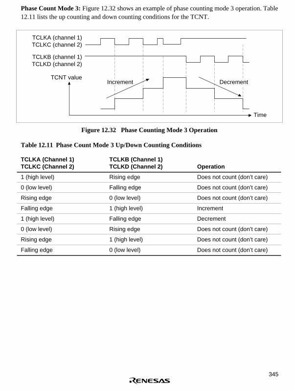
345
Phase Count Mode 3: Figure 12.32 shows an example of phase counting mode 3 operation. Table12.11 lists the up counting and down counting conditions for the TCNT.
Increment Decrement
TCLKA (channel 1)TCLKC (channel 2)
TCLKB (channel 1)TCLKD (channel 2)
TCNT value
Time
Figure 12.32 Phase Counting Mode 3 Operation
Table 12.11 Phase Count Mode 3 Up/Down Counting Conditions
TCLKA (Channel 1)TCLKC (Channel 2)
TCLKB (Channel 1)TCLKD (Channel 2) Operation
1 (high level) Rising edge Does not count (don’t care)
0 (low level) Falling edge Does not count (don’t care)
Rising edge 0 (low level) Does not count (don’t care)
Falling edge 1 (high level) Increment
1 (high level) Falling edge Decrement
0 (low level) Rising edge Does not count (don’t care)
Rising edge 1 (high level) Does not count (don’t care)
Falling edge 0 (low level) Does not count (don’t care)

346
Phase Count Mode 4: Figure 12.33 shows an example of phase counting mode 4 operation. Table12.12 lists the up counting and down counting conditions for the TCNT.
Increment Decrement
TCLKA (Channel 1)TCLKC (Channel 2)
TCLKB (Channel 1)TCLKD (Channel 2)
TCNT value
Time
Figure 12.33 Phase Counting Mode 4 Operation
Table 12.12 Phase Count Mode 4 Up/Down Counting Conditions
TCLKA (Channel 1)TCLKC (Channel 2)
TCLKB (Channel 1)TCLKD (Channel 2) Operation
1 (high level) Rising edge Increment
0 (low level) Falling edge
Rising edge 0 (low level) Does not count (don’t care)
Falling edge 1 (high level)
1 (high level) Falling edge Decrement
0 (low level) Rising edge
Rising edge 1 (high level) Does not count (don’t care)
Falling edge 0 (low level)
Phase Counting Mode Application Example: Figure 12.34 shows an example where channel 1is set to phase counting mode and is teamed with channel 0 to input a two-phase encoder pulse fora servo motor to accurately detect position and speed.
Channel 1 is set to phase counting mode 1, and the encoder pulse A phase and B phase are input tothe TCLKA and TCLKB pins.
Channel 0 is set so that the TCNT counter is cleared on a TGR0C register compare-match, and theTGR0A and TGR0C registers are used with the compare-match function to establish the speedcontrol and position control periods. The TGR0B register is used with the input capture function,and the TGR0B and TGR0D registers are employed for buffer operation. The channel 1 counter

347
input clock is used as the TGR0B register input capture source, and a pulse width of four times the2-phase encoder pulse is detected.
The channel 1 TGR1A and TGR1B registers are set for the input capture function, the channel 0TGR0A and TGR0C register compare-match is used as an input capture source, and all of thecontrol period increment and decrement values are stored.
TCLKA
TCLKB
Edgedetection
circuit
TCNT1
TCNT0
TGR1A (speedperiod capture)
TGR0A (speedcontrol period)
TGR0C (positioncontrol period)
TGR0B (pulsewidth capture)
TGR0D (bufferoperation)
TGR1B (positionperiod capture)
Channel 0
Channel 1
+–
+–
Figure 12.34 Phase Count Mode Application Example

348
12.4.8 Reset-Synchronized PWM Mode
In the reset-synchronized PWM mode, three-phase output of positive and negative PWMwaveforms that share a common wave transition point can be obtained using channels 3 and 4.
When set for reset-synchronized PWM mode, the TIOC3B, TIOC3D, TIOC4A, TIOC4C,TIOC4B, and TIOC4D pins become PWM output pins and TCNT3 becomes an upcounter.
Table 12.13 shows the PWM output pins used. Table 12.14 shows the settings of the registers.
Table 12.13 Output Pins for Reset-Synchronized PWM Mode
Channel Output Pin Description
3 TIOC3B PWM output 1
TIOC3D PWM output 1' (negative-phase waveform of PWM output 1)
4 TIOC4A PWM output 2
TIOC4C PWM output 2' (negative-phase waveform of PWM output 2)
TIOC4B PWM output 3
TIOC4D PWM output 3' (negative-phase waveform of PWM output 3)
Table 12.14 Register Settings for Reset-Synchronized PWM Mode
Register Description of Contents
TCNT3 Initial setting of H'0000
TCNT4 Initial setting of H'0000
TGR3A Set count cycle for TCNT3
TGR3B Sets the turning point for PWM waveform output by the TIOC3B and TIOC3D pins
TGR4A Sets the turning point for PWM waveform output by the TIOC4A and TIOC4C pins
TGR4B Sets the turning point for PWM waveform output by the TIOC4B and TIOC4D pins
Procedure for Selecting the Reset-Synchronized PWM Mode (Figure 12.35):
1. Clear the CST3 and CST4 bits in the TSTR to 0 to halt TCNT3 and TCNT4. The reset-synchronized PWM mode must be set up while TCNT3 and TCNT4 are halted.
2. Set bits TPSC2–TPSC0 and CKEG1 and CKEG0 in the TCR to select the counter clock andclock edge for channel 3.
3. Set bits CCLR2–CCLR0 in the TCR3 to select TGRA compare-match as a counter clearsource.

349
4. When performing brushless DC motor control, set bit BDC in the timer gate control register(TGCR) and set the feedback signal input source and output chopping or gate signal directoutput.
5. Reset TCNT3 and TCNT4 to H'0000.
6. TGR3A is the period register. Set the waveform period value in TGR3A. Set the transitiontimes of the PWM output waveforms in TGR3B, TGR4A, and TGR4B. Set times within thecompare-match range of TCNT3. X ≤ TGR3A (X: set value). With X = TGRA (cycle = dutycycle), the output waveform goes into toggle operation at the point where TCNT3 = TGR3A =X.
7. Select enabling/disabling of toggle output synchronized with the PMW cycle using bit PSYEin the timer output control register (TOCR), and set the PWM output level with bits OLSP andOLSN.
8. Set bits MD3–MD0 in TMDR3 to B'1000 to select the reset-synchronized PWM mode.TIOC3B, TIOC3D, TIOC4A, TIOC4B, TIOC4C, and TIOC4D become PWM output pins.
9. Set the CST3 bit in the TSTR to 1 to start the count operation.
10. Set the STR3 bit in the TSTR to 1 to let the TCNT3 start counting.

350
8
1
2
3
4
5
Stop counting
Select counter clock
Set TGR
Select counter clear source
Reset-synchronizedPWM mode
Brushless DC motor control setting
Set TCNT
6
Enable PWM output
Set reset-synchronizedPWM mode
7PWM cycle output enabling,PWM output level setting
9
Start count operation 10
Reset-synchronized PWM mode
Figure 12.35 Procedure for Selecting the Reset-Synchronized PWM Mode

351
Reset-Synchronized PWM Mode Operation: Figure 12.36 shows an example of operation in thereset-synchronized PWM mode. TCNT3 and TCNT4 operate as upcounters. The counter is clearedwhen a TCNT3 and TGR3A compare-match occurs, and then begins incrementing from H'0000.The PWM output pin output toggles with each occurrence of a TGR3B, TGR4A, TGR4Bcompare-match, and upon counter clears.
TGR3A
TGR3B
TGR4B
H'0000
TGR4A
TIOC3B
TIOC3D
TIOC4A
TIOC4C
TIOC4B
TIOC4D
Time
TCNT3 and TCNT4values
Figure 12.36 Reset-Synchronized PWM Mode Operation Example (When the TOCR’sOLSN = 1 and OLSP = 1)

352
12.4.9 Complementary PWM Mode
In the complementary PWM mode, three-phase output of non-overlapping positive and negativePWM waveforms can be obtained using channels 3 and 4.
In complementary PWM mode, TIOC3B, TIOC3D, TIOC4A, TIOC4B, TIOC4C, and TIOC4Dpins become PWM output pins, the TIOC3A pin can be set for toggle output synchronized withthe PWM period. TCNT3 and TCNT4 function as increment/decrement counters.
Table 12.15 shows the PWM output pins used. Table 12.16 shows the settings of the registers.
A function to directly cut off the PWM output by using an external signal is supported as a portfunction.
Table 12.15 Output Pins for Complementary PWM Mode
Channel Output Pin Description
3 TIOC3A Toggle output synchronized with PWM period (or I/O port)
TIOC3B PWM output 1
TIOC3C I/O port (Avoid setting this pin as a timer I/O pin in thecomplementary PWM mode.)
TIOC3D PWM output 1 (non-overlapping negative-phase waveform ofPWM output 1)
4 TIOC4A PWM output 2
TIOC4B PWM output 3
TIOC4C PWM output 2 (non-overlapping negative-phase waveform ofPWM output 2)
TIOC4D PWM output 3 (non-overlapping negative-phase waveform ofPWM output 3)

353
Table 12.16 Register Settings for Complementary PWM Mode
Channel Counter/Register Description Read/Write from CPU
3 TCNT3 Start of up-count from value setin dead time register
Maskable by BSC/BCR1setting*
TGR3A Set TCNT3 upper limit value(1/2 carrier cycle + dead time)
Maskable by BSC/BCR1setting*
TGR3B PWM output 1 compare register Maskable by BSC/BCR1setting*
TGR3C TGR3A buffer register Always readable/writable
TGR3D PWM output 1/TGR3B bufferregister
Always readable/writable
4 TCNT4 Up-count start, initialized toH'0000
Maskable by BSC/BCR1setting*
TGR4A PWM output 2 compare register Maskable by BSC/BCR1setting*
TGR4B PWM output 3 compare register Maskable by BSC/BCR1setting*
TGR4C PWM output 2/TGR4A bufferregister
Always readable/writable
TGR4D PWM output 3/TGR4B bufferregister
Always readable/writable
Timer dead time data register(TDDR)
Set TCNT4 and TCNT3 offsetvalue (dead time value)
Maskable by BSC/BCR1setting*
Timer cycle data register(TCDR)
Set TCNT4 upper limit value(1/2 carrier cycle)
Maskable by BSC/BCR1setting*
Timer cycle buffer register(TCBR)
TCDR buffer register Always readable/writable
Subcounter (TCNTS) Subcounter for dead timegeneration
Read-only
Temporary register 1 (TEMP1) PWM output 1/TGR3B temporaryregister
Not readable/writable
Temporary register 2 (TEMP2) PWM output 2/TGR4A temporaryregister
Not readable/writable
Temporary register 3 (TEMP3) PWM output 3/TGR4B temporaryregister
Not readable/writable
Note: * Access can be enabled or disabled according to the setting of bit 13 (MTURWE) inBSC/BCR1 (bus controller/bus control register 1).

354
@À@À@À@À@À@À@À@À@À@À@À@@ÀÀ@@ÀÀ@@ÀÀ@@ÀÀ@@ÀÀ@@ÀÀ@@ÀÀ@@ÀÀ@@ÀÀ@@ÀÀ@@ÀÀ@@ÀÀ@@ÀÀ@@ÀÀ@@ÀÀ@@ÀÀ@@ÀÀ@@ÀÀ@@ÀÀ@@ÀÀ@@ÀÀ@@ÀÀ@@ÀÀ@@ÀÀ@@ÀÀ@@ÀÀ@@ÀÀ@@ÀÀ@@ÀÀ@@ÀÀ@@ÀÀ@@ÀÀ@@ÀÀ@@ÀÀ@@ÀÀ@@ÀÀ@@ÀÀ@@ÀÀ@@ÀÀ@@ÀÀ@@ÀÀ@@ÀÀ@@ÀÀ@@ÀÀ
@@ÀÀ@@ÀÀ@@ÀÀ@@ÀÀ@@ÀÀ@@ÀÀ@@ÀÀ@@ÀÀ@@ÀÀ@@ÀÀ@@ÀÀ@@ÀÀ@@ÀÀ@@ÀÀ@@ÀÀ@@ÀÀ@@ÀÀ@@ÀÀ@@ÀÀ@@ÀÀ@@ÀÀ@@ÀÀ@@@@ÀÀÀÀ@@@@ÀÀÀÀ@@@@ÀÀÀÀ@@@@ÀÀÀÀ@@@@ÀÀÀÀ@@@@ÀÀÀÀ@@@@ÀÀÀÀ@@@@ÀÀÀÀ@@@@ÀÀÀÀ@@@@ÀÀÀÀ@@@@ÀÀÀÀ
@À@À@À@À@À@À@À@À@À@À@À
TGR3C
TDDR
TCNT3
TGR3D TGR4DTGR4C
TG
R3B
Tem
p 1
TG
R4A
Tem
p 2
TG
R4B
Tem
p 3
TCNTS TCNT4
TGR3A TCDR
TCBR
Comparator
Comparator
Matchsignal
Matchsignal
Out
put c
ontr
olle
r
Out
put p
rote
ctio
n ci
rcui
t
PWM cycle output
PWM output 1PWM output 2PWM output 3PWM output 4PWM output 5PWM output 6
POE0POE1POE2POE3
External cutoff input
External cutoff interrupt
: Registers that can always be read or written from the CPU
: Registers that cannot be read or written from the CPU (except for TCNTS, which can only be read)
: Registers that can be read or written from the CPU (but for which access disabling can be set by the bus controller)
TG
R3A
com
pare
-m
atch
inte
rrup
t
TC
NT
4 un
derf
low
in
terr
upt
Figure 12.37 Block Diagram of Channels 3 and 4 in Complementary PWM Mode

355
Example of Complementary PWM Mode Setting Procedure: An example of thecomplementary PWM mode setting procedure is shown in figure 12.38.
1. Clear bits CST3 and CST4 in the timer start register (TSTR) to 0, and halt timer counter(TCNT) operation. Perform complementary PWM mode setting when TCNT3 and TCNT4 arestopped.
2. Set the same counter clock and clock edge for channels 3 and 4 with bits TPSC2–TPSC0 andbits CKEG1 and CKEG0 in the timer control register (TCR). Use bits CCLR2–CCLR0 to setsynchronous clearing only when restarting by a synchronous clear from another channel duringcomplementary PWM mode operation.
3. When performing brushless DC motor control, set bit BDC in the timer gate control register(TGCR) and set the feedback signal input source and output chopping or gate signal directoutput.
4. Set the dead time in TCNT3. Set TCNT4 to H'0000.
5. Set only when restarting by a synchronous clear from another channel during complementaryPWM mode operation. In this case, synchronize the channel generating the synchronous clearwith channels 3 and 4 using the timer synchro register (TSYR).
6. Set the output PWM duty in the duty registers (TGR3B, TGR4A, TGR4B) and buffer registers(TGR3D, TGR4C, TGR4D). Set the same initial value in each corresponding TGR.
7. Set the dead time in the dead time register (TDDR), 1/2 the carrier cycle in the carrier cycledata register (TCDR) and carrier cycle buffer register (TCBR), and 1/2 the carrier cycle plusthe dead time in TGR3A and TGR3C.
8. Select enabling/disabling of toggle output synchronized with the PWM cycle using bit PSYEin the timer output control register (TOCR), and set the PWM output level with bits OLSP andOLSN.
9. Select complementary PWM mode in timer mode register 3 (TMDR3). Pins TIOC3A,TIOC3B, TIOC3D, TIOC4A, TIOC4B, TIOC4C, and TIOC4D function as output pins. Do notset in TMDR4.
10. Set enabling/disabling of PWM waveform output pin output in the timer output master enableregister (TOER).
11. Set bits CST3 and CST4 in TSTR to 1 simultaneously to start the count operation.

356
Complementary PWM mode
Stop count operation
Counter clock, counter clearsource selection
Brushless DC motor controlsetting
TCNT setting
Inter-channel cycle setting
TGR setting
Dead time, carrier cyclesetting
PWM cycle output enabling,PWM output level setting
Complementary PWM modesetting
3
Enable waveform output
Start count operation
<Complementary PWM mode>
2
4
5
6
7
8
9
10
11
1
Figure 12.38 Example of Complementary PWM Mode Setting Procedure

357
Outline of Complementary PWM Mode Operation: In complementary PWM mode, 6-phasePWM output is possible. Figure 12.39 illustrates counter operation in complementary PWMmode, and figure 12.40 shows an example of complementary PWM mode operation.
• Counter operation
In complementary PWM mode, three counters—TCNT3, TCNT4, and TCNTS—performup/down-count operations.
TCNT3 is automatically initialized to the value set in TDDR when complementary PWMmode is selected and the CST bit in TSTR is 0.
When the CST bit is set to 1, TCNT3 counts up to the value set in TGR3A, then switches todown-counting when it matches TGR3A,. When the TCNT3 value matches TDDR, the counterswitches to up-counting, and the operation is repeated in this way.
TCNT4 is initialized to H'0000.
When the CST bit is set to 1, TCNT4 counts up in synchronization with TCNT3, and switchesto down-counting when it matches TCDR . On reaching H'0000, TCNT4 switches to up-counting, and the operation is repeated in this way.
TCNTS is a read-only counter. It need not be initialized.
When TCNT3 matches TCDR during TCNT3 and TCNT4 up/down-counting, down-countingis started, and when TCNTS matches TCDR, the operation switches to up-counting. WhenTCNTS matches TGR3A, it is cleared to H'0000.
When TCNT4 matches TDDR during TCNT3 and TCNT4 down-counting, up-counting isstarted, and when TCNTS matches TDDR, the operation switches to down-counting. WhenTCNTS reaches H'0000, it is set with the value in TGR3A.
TCNTS is compared with the compare register and temporary register in which the PWM dutyis set during the count operation only.
Counter value
TGR3A
TCDR
TDDR
H'0000
TCNT4 TCNTS
TCNT3
TCNT3
TCNT4
TCNTS
Time
Figure 12.39 Complementary PWM Mode Counter Operation
358
• Register operation
In complementary PWM mode, nine registers are used, comprising compare registers, bufferregisters, and temporary registers. Figure 12.40 shows an example of complementary PWMmode operation.
The registers which are constantly compared with the counters to perform PWM output areTGR3B, TGR4A, and TGR4B. When these registers match the counter, the value set in bitsOLSN and OLSP in the timer output control register (TOCR) is output.
The buffer registers for these compare registers are TGR3D, TGR4C, and TGR4D.
Between a buffer register and compare register there is a temporary register. The temporaryregisters cannot be accessed by the CPU.
Data in a compare register is changed by writing the new data to the corresponding bufferregister. The buffer registers can be read or written at any time.
The data written to a buffer register is constantly transferred to the temporary register in the Tainterval. Data is not transferred to the temporary register in the Tb interval. Data written to abuffer register in this interval is transferred to the temporary register at the end of the Tbinterval.
The value transferred to a temporary register is transferred to the compare register whenTCNTS for which the Tb interval ends matches TGR3A when counting up, or H'0000 whencounting down. The timing for transfer from the temporary register to the compare register canbe selected with bits MD3–MD0 in the timer mode register (TMDR). Figure 12.40 shows anexample in which the mode is selected in which the change is made in the trough.
In the tb interval (tb2 in figure 12.40) in which data transfer to the temporary register is notperformed, the temporary register has the same function as the compare register, and iscompared with the counter. In this interval, therefore, there are two compare registers for one-phase output, with the compare register containing the pre-change data, and the temporaryregister containing the new data. In this interval, the three counters—TCNT3, TCNT4, andTCNTS—and two registers—compare register and temporary register—are compared, andPWM output controlled accordingly.

359
TGR3A
TCDR
TGR4A
TGR4C
TDDR
H'0000
Buffer registerTGR4C
Temporary registerTEMP2
Compare registerTGR4A
Output waveform
Output waveform
Tb2 Ta Tb1 Ta Tb2 Ta
TCNT3
TCNT4
TCNTS
(Output waveform is active-low)
H'6400 H'0080
H'6400
H'6400 H'0080
H'0080
Transfer from temporary register to compare register
Transfer from temporary register to compare register
Figure 12.40 Example of Complementary PWM Mode Operation
360
• Initialization
In complementary PWM mode, there are six registers that must be initialized.
Before setting complementary PWM mode with bits MD3–MD0 in the timer mode register(TMDR), the following initial register values must be set.
TGR3C operates as the buffer register for TGR3A, and should be set with 1/2 the PWM carriercycle + dead time Td. The timer cycle buffer register (TCBR) operates as the buffer register forthe timer cycle data register (TCDR), and should be set with 1/2 the PWM carrier cycle. Setdead time Td in the timer dead time data register (TDDR).
Set the respective initial PWM duty values in buffer registers TGR3D, TGR4C, and TGR4D.
The values set in the five buffer registers excluding TDDR are transferred simultaneously tothe corresponding compare registers when complementary PWM mode is set.
Set TCNT4 to H'0000 before setting complementary PWM mode.
Table 12.17 Registers and Counters Requiring Initialization
Register/Counter Set Value
TGR3C 1/2 PWM carrier cycle + dead time Td
TDDR Dead time Td
TCBR 1/2 PWM carrier cycle
TGR3D, TGR4C, TGR4D Initial PWM duty value for each phase
TCNT4 H'0000
Note: The TGR3C set value must be the sum of 1/2 the PWM carrier cycle set in TCBR and deadtime Td set in TDDR.
• PWM output level setting
In complementary PWM mode, the PWM pulse output level is set with bits OLSN and OLSPin the timer output control register (TOCR).
The output level can be set for each of the three positive phases and three negative phases of 6-phase output.
Complementary PWM mode should be cleared before setting or changing output levels.
• Dead time setting
In complementary PWM mode, PWM pulses are output with a non-overlapping relationshipbetween the positive and negative phases. This non-overlap time is called the dead time.
The non-overlap time is set in the timer dead time data register (TDDR). The value set inTDDR is used as the TCNT3 counter start value, and creates non-overlap between TCNT3 andTCNT4. Complementary PWM mode should be cleared before changing the contents ofTDDR.

361
• PWM cycle setting
In complementary PWM mode, the PWM pulse cycle is set in two registers—TGR3A, inwhich the TCNT3 upper limit value is set, and TCDR, in which the TCNT4 upper limit valueis set. The settings should be made so as to achieve the following relationship between thesetwo registers:
TGR3A set value = TCDR set value + TDDR set value
The TGR3A and TCDR settings are made by setting the values in buffer registers TGR3C andTCBR. The values set in TGR3C and TCBR are transferred simultaneously to TGR3A andTCDR in accordance with the transfer timing selected with bits MD3–MD0 in the timer moderegister (TMDR).
The updated PWM cycle is reflected from the next cycle when the data update is performed atthe crest, and from the current cycle when performed in the trough. Figure 12.41 illustrates theoperation when the PWM cycle is updated at the crest.
See the following section, Register data updating, for the method of updating the data in eachbuffer register.
Counter valueTGR3Cupdate
TGR3Aupdate
TGR3A
TCNT3
TCNT4
Time
Figure 12.41 Example of PWM Cycle Updating

362
• Register data updating
In complementary PWM mode, the buffer register is used to update the data in a compareregister. The update data can be written to the buffer register at any time. There are five PWMduty and carrier cycle registers that have buffer registers and can be updated during operation.
There is a temporary register between each of these registers and its buffer register. Whensubcounter TCNTS is not counting, if buffer register data is updated, the temporary registervalue is also rewritten. Transfer is not performed from buffer registers to temporary registerswhen TCNTS is counting; in this case, the value written to a buffer register is transferred afterTCNTS halts.
The temporary register value is transferred to the compare register at the data update timing setwith bits MD3–MD0 in the timer mode register (TMDR). Figure 12.42 shows an example ofdata updating in complementary PWM mode. This example shows the mode in which dataupdating is performed at both the counter crest and trough.
When rewriting buffer register data, a write to TGR4D must be performed at the end of the update. Data transfer from the buffer registers to the temporary registers is performed simultaneously for all five registers after the write to TGR4D.
A write to TGR4D must be performed after writing data to the registers to be updated, evenwhen not updating all five registers, or when updating the TGR4D data. In this case, the datawritten to TGR4D should be the same as the data prior to the write operation.
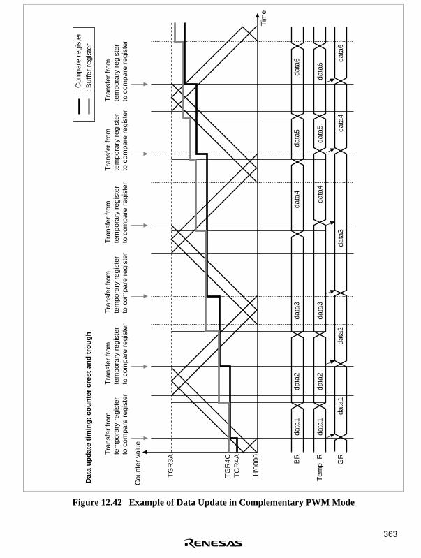
363
Dat
a up
date
tim
ing:
cou
nter
cre
st a
nd tr
ough
Tra
nsfe
r fr
om
tem
pora
ry r
egis
ter
to
com
pare
reg
iste
r
Tra
nsfe
r fr
om
tem
pora
ry r
egis
ter
to
com
pare
reg
iste
r
Tra
nsfe
r fr
om
tem
pora
ry r
egis
ter
to
com
pare
reg
iste
r
Tra
nsfe
r fr
om
tem
pora
ry r
egis
ter
to
com
pare
reg
iste
r
Tra
nsfe
r fr
om
tem
pora
ry r
egis
ter
to
com
pare
reg
iste
r
Tra
nsfe
r fr
om
tem
pora
ry r
egis
ter
to
com
pare
reg
iste
r
Cou
nter
val
ue
TG
R3A
TG
R4C
TG
R4A
H'0
000
BR
data
1da
ta2
data
3da
ta4
data
5da
ta6
data
1
data
1da
ta2
data
3da
ta4
data
6
data
2da
ta3
data
4da
ta5
data
6T
emp_
R
GR
Tim
e
: Com
pare
reg
iste
r
: Buf
fer
regi
ster
Figure 12.42 Example of Data Update in Complementary PWM Mode

364
• Initial output in complementary PWM mode
In complementary PWM mode, the initial output is determined by the setting of bits OLSN andOLSP in the timer output control register (TOCR).
This initial output is the PWM pulse non-active level, and is output from when complementaryPWM mode is set with the timer mode register (TMDR) until TCNT4 exceeds the value set inthe dead time register (TDDR). Figure 12.43 shows an example of the initial output incomplementary PWM mode.
An example of the waveform when the initial PWM duty value is smaller than the TDDRvalue is shown in figure 12.44.
Timer output control register settings
OLSN bit: 0 (initial output: high; active level: low)OLSP bit: 0 (initial output: high; active level: low)
TCNT3, 4 value
TGR4A
TDDR
TCNT3
TCNT4
Initial output Dead timeTime
Active level
Active level
TCNT3, 4 count start(TSTR setting)
Complementary PWM mode(TMDR setting)
Positive phaseoutput
Negative phaseoutput
Figure 12.43 Example of Initial Output in Complementary PWM Mode (1)

365
Timer output control register settings
OLSN bit: 0 (initial output: high; active level: low)OLSP bit: 0 (initial output: high; active level: low)
TCNT3, 4 value
TGR4ATDDR
TCNT3
TCNT4
Initial outputTime
Active level
TCNT3, 4 count start(TSTR setting)
Complementary PWM mode(TMDR setting)
Positive phaseoutput
Negative phaseoutput
Figure 12.44 Example of Initial Output in Complementary PWM Mode (2)
366
• Complementary PWM mode PWM output generation method
In complementary PWM mode, 3-phase output is performed of PWM waveforms with a non-overlap time between the positive and negative phases. This non-overlap time is called thedead time.
A PWM waveform is generated by output of the output level selected in the timer outputcontrol register in the event of a compare-match between a counter and data register. WhileTCNTS is counting, data register and temporary register values are simultaneously comparedto create consecutive PWM pulses from 0 to 100%. The relative timing of on and off compare-match occurrence may vary, but the compare-match that turns off each phase takes precedence to secure the dead time and ensure that the positive phase and negative phase on times do not overlap. Figures 12.45 to 12.47 show examples of waveform generation in complementaryPWM mode.
The positive phase/negative phase off timing is generated by a compare-match with the solid-line counter, and the on timing by a compare-match with the dotted-line counter operating witha delay of the dead time behind the solid-line counter. In the T1 period, compare-match a thatturns off the negative phase has the highest priority, and compare-matches occurring prior to aare ignored. In the T2 period, compare-match c that turns off the positive phase has the highestpriority, and compare-matches occurring prior to c are ignored.
In normal cases, compare-matches occur in the order a → b → c → d (or c → d → a' → b'),as shown in figure 12.45.
If compare-matches deviate from the a → b → c → d order, since the time for which thenegative phase is off is less than twice the dead time, the figure shows the positive phase as notbeing turned on. If compare-matches deviate from the c → d → a' → b' order, since the timefor which the positive phase is off is less than twice the dead time, the figure shows thenegative phase as not being turned on.
If compare-match c occurs first following compare-match a, as shown in figure 12.46,compare-match b is ignored, and the negative phase is turned off by compare-match d. This isbecause turning off of the positive phase has priority due to the occurrence of compare-match c(positive phase off timing) before compare-match b (positive phase on timing) (consequently,the waveform does not change since the positive phase goes from off to off).
Similarly, in the example in figure 12.47, compare-match a' with the new data in thetemporary register occurs before compare-match c, but other compare-matches occurring up toc, which turns of the positive phase, are ignored. As a result, the positive phase is not turnedon.
Thus, in complementary PWM mode, compare-matches at turn-off timings take precedence,and turn-on timing compare-matches that occur before a turn-off timing compare-match areignored.

367
T2 periodT1 period T1 period
a b
c
a' b'
d
TGR3A
TCDR
TDDR
H'0000
Positive phase
Negative phase
Figure 12.45 Example of Complementary PWM Mode Waveform Output (1)
T2 periodT1 period T1 period
TGR3A
TCDR
TDDR
H'0000
Positive phase
Negative phase
c d
a
a
b
b
Figure 12.46 Example of Complementary PWM Mode Waveform Output (2)

368
a b
c
a' b'
d
T1 period T2 period T1 period
TGR3A
TCDR
TDDR
H'0000
Positive phase
Negative phase
Figure 12.47 Example of Complementary PWM Mode Waveform Output (3)
a b
c d
a' b'
T2 periodT1 period T1 period
TGR3A
TCDR
TDDR
H'0000
Positive phase
Negative phase
Figure 12.48 Example of Complementary PWM Mode 0% and 100% Waveform Output (1)

369
T2 periodT1 period T1 period
TGR3A
TCDR
TDDR
H'0000
Positive phase
Negative phase
a
c d
a b
b
Figure 12.49 Example of Complementary PWM Mode 0% and 100% Waveform Output (2)
T2 periodT1 period T1 period
a b
c dTGR3A
TCDR
TDDR
H'0000
Positive phase
Negative phase
Figure 12.50 Example of Complementary PWM Mode 0% and 100% Waveform Output (3)

370
TGR3A
TCDR
TDDR
H'0000
Positive phase
Negative phase
T2 periodT1 period T1 period
a b
c b' d a'
Figure 12.51 Example of Complementary PWM Mode 0% and 100% Waveform Output (4)
c a d bT2 periodT1 period T1 period
TGR3A
TCDR
TDDR
H'0000
Positive phase
Negative phase
Figure 12.52 Example of Complementary PWM Mode 0% and 100% Waveform Output (5)

371
• Complementary PWM mode 0% and 100% duty output
In complementary PWM mode, 0% and 100% duty cycles can be output as required. Figures12.48 to 12.52 show output examples.
100% duty output is performed when the data register value is set to H'0000. The waveform inthis case has a positive phase with a 100% on-state. 0% duty output is performed when the dataregister value is set to the same value as TGR3A. The waveform in this case has a positivephase with a 100% off-state.
On and off compare-matches occur simultaneously, but if a turn-on compare-match and turn-off compare-match for the same phase occur simultaneously, both compare-matches areignored and the waveform does not change.
• Toggle output synchronized with PWM cycle
In complementary PWM mode, toggle output can be performed in synchronization with thePWM carrier cycle by setting the PSYE bit to 1 in the timer output control register (TOCR).An example of a toggle output waveform is shown in figure 12.53.
This output is toggled by a compare-match between TCNT3 and TGR3A and a compare-matchbetween TCNT4 and H'0000.
The output pin for this toggle output is the TIOC3A pin. The initial output is 1.
TGR3A
H'0000
Toggle output
TIOC3A pin
TCNT4
TCNT3
Figure 12.53 Example of Toggle Output Waveform Synchronized with PWM Output

372
• Counter clearing by another channel
In complementary PWM mode, by setting a mode for synchronization with another channel bymeans of the timer synchro register (TSYR), and selecting synchronous clearing with bitsCCLR2–CCLR0 in the timer control register (TCR), it is possible to have TCNT3, TCNT4,and TCNTS cleared by another channel.
Figure 12.54 illustrates the operation.
Use of this function enables counter clearing and restarting to be performed by means of anexternal signal.
TGR3A
TCDR
TDDR
H'0000
Channel 1 input capture A
TCNT1
TCNT3
TCNT4
TCNTS
Synchronous counter clearing by channel 1 input capture A
Figure 12.54 Counter Clearing Synchronized with Another Channel

373
• Example of AC synchronous motor (brushless DC motor) drive waveform output
In complementary PWM mode, a brushless DC motor can easily be controlled using the timergate control register (TGCR). Figures 12.55 to 12.58 show examples of brushless DC motordrive waveforms created using TGCR.
When output phase switching for a 3-phase brushless DC motor is performed by means ofexternal signals detected with a Hall element, etc., clear the FB bit in TGCR to 0. In this case,the external signals indicating the polarity position are input to channel 0 timer input pinsTIOC0A, TIOC0B, and TIOC0C (set with PFC). When an edge is detected at pin TIOC0A,TIOC0B, or TIOC0C, the output on/off state is switched automatically.
When the FB bit is 1, the output on/off state is switched when the UF, VF, or WF bit in TGCRis cleared to 0 or set to 1.
The drive waveforms are output from the complementary PWM mode 6-phase output pins.With this 6-phase output, in the case of on output, it is possible to use complementary PWMmode output and perform chopping output by setting the N bit or P bit to 1. When the N bit orP bit is 0, level output is selected.
The 6-phase output active level (on output level) can be set with the OLSN and OLSP bits inthe timer output control register (TOCR) regardless of the setting of the N and P bits. Whenusing this mode, set the 6-phase output waveform to High active (Low active is also permittedfor A masks).
External input TIOC0A pin
TIOC0B pin
TIOC0C pin
TIOC3B pin
TIOC3D pin
TIOC4A pin
TIOC4C pin
TIOC4B pin
TIOC4D pin
6-phase output
When BDC = 1, N = 0, P = 0, FB = 0, output active level = high
Figure 12.55 Example of Output Phase Switching by External Input (1)

374
External input TIOC0A pin
TIOC0B pin
TIOC0C pin
TIOC3B pin
TIOC3D pin
TIOC4A pin
TIOC4C pin
TIOC4B pin
TIOC4D pin
6-phase output
When BDC = 1, N = 1, P = 1, FB = 0, output active level = high
Figure 12.56 Example of Output Phase Switching by External Input (2)
TGCR UF bit
VF bit
WF bit
TIOC3B pin
TIOC3D pin
TIOC4A pin
TIOC4C pin
TIOC4B pin
TIOC4D pin
6-phase output
When BDC = 1, N = 0, P = 0, FB = 0, output active level = high
Figure 12.57 Example of Output Phase Switching by Means of UF, VF, WF Bit Settings (1)

375
TGCR UF bit
VF bit
WF bit
TIOC3B pin
TIOC3D pin
TIOC4A pin
TIOC4C pin
TIOC4B pin
TIOC4D pin
6-phase output
When BDC = 1, N = 1, P = 1, FB = 0, output active level = high
Figure 12.58 Example of Output Phase Switching by Means of UF, VF, WF Bit Settings (2)
• A/D conversion start request setting
In complementary PWM mode, an A/D conversion start request can be issued using a TGR3Acompare-match or a compare-match on a channel other than channels 3 and 4.
When start requests using a TGR3A compare-match are set, A/D conversion can be started atthe center of the PWM pulse.
A/D conversion start requests can be set by setting the TTGE bit to 1 in the timer interruptenable register (TIER).

376
Complementary PWM Mode Output Protection Function: Complementary PWM mode outputhas the following protection functions.
• Register and counter miswrite prevention function
With the exception of the buffer registers, which can be rewritten at any time, access by theCPU can be enabled or disabled for the mode registers, control registers, compare registers,and counters used in complementary PWM mode by means of bit 13 in the bus controller’s buscontrol register 1 (BCR1). The registers and counters concerned are listed in table 12.3.
This function enables miswriting due to CPU runaway to be prevented by disabling CPUaccess to the mode registers, control registers, and counters.
• Halting of PWM output by external signal
The 6-phase PWM output pins can be set automatically to the high-impedance state byinputting specified external signals. There are four external signal input pins.
See section 12.9, Port Output Enable (POE), for details.
• Halting of PWM output when oscillator is stopped
If it is detected that the clock input to the SH7040 chip has stopped, the 6-phase PWM outputpins automatically go to the high-impedance state. The pin states are not guaranteed when theclock is restarted.
See section 4.4, Oscillator Halt Function, for details.

377
12.5 Interrupts
12.5.1 Interrupt Sources and Priority Ranking
The MTU has three interrupt sources: TGR register compare-match/input captures, TCNT counteroverflows and TCNT counter underflows. Because each of these three types of interrupts areallocated its own dedicated status flag and enable/disable bit, the issuing of interrupt requestsignals to the interrupt controller can be independently enabled or disabled.
When an interrupt source is generated, the corresponding status flag in the timer status register(TSR) is set to 1. If the corresponding enable/disable bit in the timer input enable register (TIER)is set to 1 at this time, the MTU makes an interrupt request of the interrupt controller. Theinterrupt request is canceled by clearing the status flag to 0.
The channel priority order can be changed with the interrupt controller. The priority rankingwithin a channel is fixed. For more information, see section 6, Interrupt Controller (INTC).
Table 12.17 lists the MTU interrupt sources.
Input Capture/Compare Match Interrupts: If the TGIE bit of the timer input enable register(TIER) is already set to 1 when the TGF flag in the timer status register (TSR) is set to 1 by a TGRregister input capture/compare-match of any channel, an interrupt request is sent to the interruptcontroller. The interrupt request is canceled by clearing the TGF flag to 0. The MTU has 16 inputcapture/compare-match interrupts; four each for channels 0, 3, and 4, and two each for channels 1and 2.
Overflow Interrupts: If the TCIEV bit of the TIER is already set to 1 when the TCFV flag in theTSR is set to 1 by a TCNT counter overflow of any channel, an interrupt request is sent to theinterrupt controller. The interrupt request is canceled by clearing the TCFV flag to 0. The MTUhas five overflow interrupts, one for each channel.
Underflow Interrupts: If the TCIEU bit of the TIER is already set to 1 when the TCFU flag inthe TSR is set to 1 by a TCNT counter underflow of any channel, an interrupt request is sent to theinterrupt controller. The interrupt request is canceled by clearing the TCFU flag to 0. The MTUhas two underflow interrupts, one each for channels 1 and 2.

378
Table 12.17 MTU Interrupt Sources
ChannelInterruptSource Description
DMACActivation
DTCActivation Priority *
0 TGI0A TGR0A input capture/compare-match Yes Yes High
TGI0B TGR0B input capture/compare-match No Yes
TGI0C TGR0C input capture/compare-match No Yes
TGI0D TGR0D input capture/compare-match No Yes
TCI0V TCNT0 overflow No No
1 TGI1A TGR1A input capture/compare-match Yes Yes
TGI1B TGR1B input capture/compare-match No Yes
TCI1V TCNT1 overflow No No
TCI1U TCNT1 underflow No No
2 TGI2A TGR2A input capture/compare-match Yes Yes
TGI2B TGR2B input capture/compare-match No Yes
TCI2V TCNT2 overflow No No
TCI2U TCNT2 underflow No No
3 TGI3A TGR3A input capture/compare-match Yes Yes
TGI3B TGR3B input capture/compare-match No Yes
TGI3C TGR3C input capture/compare-match No Yes
TGI3D TGR3D input capture/compare-match No Yes
TCI3V TCNT3 overflow No No
4 TGI4A TGR4A input capture/compare-match Yes Yes
TGI4B TGR4B input capture/compare-match No Yes
TGI4C TGR4C input capture/compare-match No Yes
TGI4D TGR4D input capture/compare-match No Yes
TCI4V TCNT overflow/underflow No Yes Low
Note: * Indicates the initial status following reset. The ranking of channels can be altered usingthe interrupt controller.

379
12.5.2 DTC/DMAC Activation
DTC Activation: The TGR register input capture/compare-match interrupt of any channel can beused as a source to activate the on-chip data transfer controller (DTC). For details, refer to section8, Data Transfer Controller (DTC).
The MTU has 17 input capture/compare-match interrupts that can be used as DTC activationsources, four each for channels 0 and 3, two each for channels 1 and 2, and five for channel 4.
DMAC Activation: The TGRA register input capture/compare-match interrupt of any channelcan be used as a source to activate the on-chip DMAC. For details, refer to section 11, DirectMemory Access Controller (DMAC).
The MTU has 5 TGRA register input capture/compare-match interrupts, one for any channel, thatcan be used as DMAC activation sources.
12.5.3 A/D Converter Activation
The TGRA register input capture/compare-match of any channel can be used to activate the on-chip A/D converter.
If the TTGE bit of the TIER is already set to 1 when the TGFA flag in the TSR is set to 1 by aTGRA register input capture/compare-match of any of the channels, an A/D conversion startrequest is sent to the A/D converter. If the MTU conversion start trigger is selected at such a timeon the A/D converter side when this happens, the A/D conversion starts.
The MTU has 5 TGRA register input capture/compare-match interrupts, one for each channel, thatcan be used as A/D converter activation sources.

380
12.6 Operation Timing
12.6.1 Input/Output Timing
TCNT Count Timing: Count timing for the TCNT counter with internal clock operation is shownin figure 12.59. Count timing with external clock operation (normal mode) is shown in figure12.60, and figure 12.61 shows count timing with external clock operation (phase counting mode).
TCNTinputclock
Internalclock
TCNT
φ
Falling edge Falling edgeRising edge
N – 1 N N + 1 N + 2
Figure 12.59 TCNT Count Timing during Internal Clock Operation
TCNTinputclock
Externalclock
TCNT
φ
Falling edge Falling edgeRising edge
N – 1 N N + 1 N + 2
Figure 12.60 TCNT Count Timing during External Clock Operation (Normal Mode)
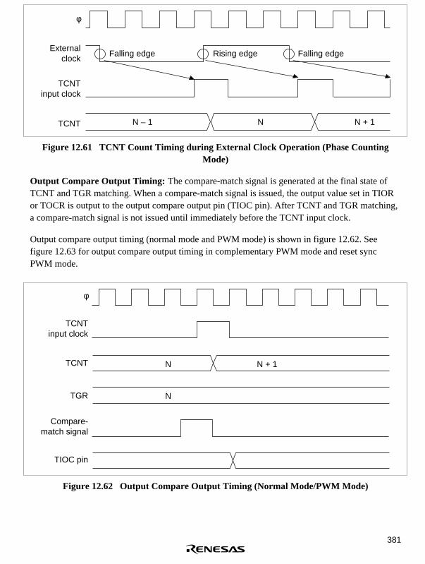
381
TCNTinput clock
Externalclock
TCNT
φ
Falling edge Falling edgeRising edge
N – 1 N N + 1
Figure 12.61 TCNT Count Timing during External Clock Operation (Phase CountingMode)
Output Compare Output Timing: The compare-match signal is generated at the final state ofTCNT and TGR matching. When a compare-match signal is issued, the output value set in TIORor TOCR is output to the output compare output pin (TIOC pin). After TCNT and TGR matching,a compare-match signal is not issued until immediately before the TCNT input clock.
Output compare output timing (normal mode and PWM mode) is shown in figure 12.62. Seefigure 12.63 for output compare output timing in complementary PWM mode and reset syncPWM mode.
TCNTinput clock
TIOC pin
Compare-match signal
TCNT
TGR
φ
N
N
N + 1
Figure 12.62 Output Compare Output Timing (Normal Mode/PWM Mode)

382
TCNTinput clock
TIOC pin
Compare-match signal
TCNT
TGR
φ
N
N
N + 1
Figure 12.63 Output Compare Output Timing (Complementary PWM Mode/Reset SyncPWM Mode)
Input Capture Signal Timing: Figure 12.64 illustrates input capture timing.
Input captureinput
Input capturesignal
TCNT
TGR
φ
N N + 2
N N + 2
N + 1
Rising edge Falling edge
Figure 12.64 Input Capture Input Signal Timing

383
Counter Clearing Timing Due to Compare-Match/Input Capture: Timing for counter clearingdue to compare-match is shown in figure 12.65. Figure 12.66 shows the timing for counterclearing due to input capture.
Compare-match signal
φ
Counterclear signal
TCNT
TGR
N
N
H'0000
Figure 12.65 Counter Clearing Timing (Compare-Match)
Inputcapture signal
φ
Counterclear signal
TCNT
TGR
N
N
H'0000
Figure 12.66 Counter Clearing Timing (Input Capture)
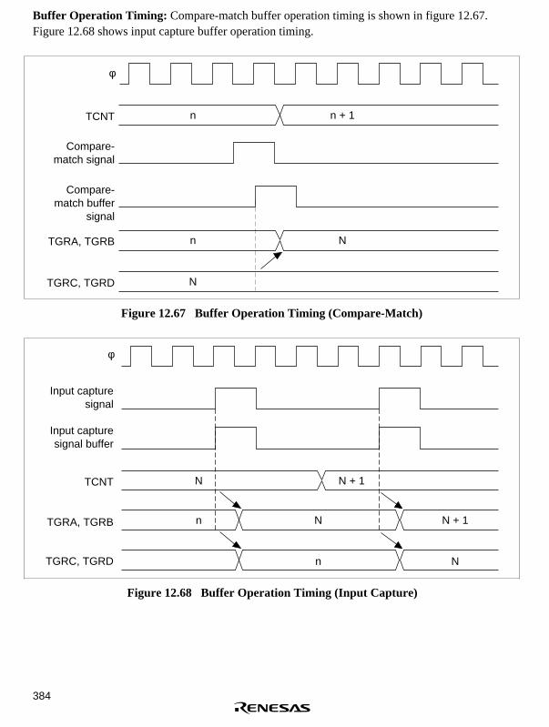
384
Buffer Operation Timing: Compare-match buffer operation timing is shown in figure 12.67.Figure 12.68 shows input capture buffer operation timing.
TCNT
φ
Compare-match buffer
signal
TGRA, TGRB
TGRC, TGRD
n n + 1
n N
N
Compare-match signal
Figure 12.67 Buffer Operation Timing (Compare-Match)
TCNT
φ
Input capturesignal buffer
TGRA, TGRB
TGRC, TGRD
N N + 1
n N
n
N + 1
N
Input capturesignal
Figure 12.68 Buffer Operation Timing (Input Capture)

385
12.6.2 Interrupt Signal Timing
Setting TGF Flag Timing during Compare-Match: Figure 12.69 shows timing for the TGF flagof the timer status register (TSR) due to compare-match, as well as TGI interrupt request signaltiming.
Compare-match signal
TCNT
TCNTinput clock
φ
TGR
TGF flag
TGI interrupt
N
N + 1N
Figure 12.69 TGI Interrupt Timing (Compare Match)
Setting TGF Flag Timing during Input Capture: Figure 12.70 shows timing for the TGF flagof the timer status register (TSR) due to input capture, as well as TGI interrupt request signaltiming.

386
Input capturesignal
TCNT
φ
TGR
TGF flag
TGI interrupt
N
N
Figure 12.70 TGI Interrupt Timing (Input Capture)
Setting Timing for Overflow Flag (TCFV)/Underflow Flag (TCFU): Figure 12.71 showstiming for the TCFV flag of the timer status register (TSR) due to overflow, as well as TCIVinterrupt request signal timing. Figure 12.72 shows timing for the TCFU flag of the timer statusregister (TSR) due to underflow, as well as TCIU interrupt request signal timing. Figure 12.73shows timing for the TCFV flag of TSR4 due to underflow in complementary PWM mode, as wellas TCIV interrupt request signal timing.
Overflowsignal
TCNT(underflow)
TCNTinput clock
φ
TCFV flag
TCIV interrupt
H'FFFF H'0000
Figure 12.71 TCIV Interrupt Setting Timing

387
Underflowsignal
TCNT(underflow)
TCNTinput clock
φ
TCFU flag
TCIU interrupt
H'0000 H'FFFF
Figure 12.72 TCIU Interrupt Setting Timing
Underflowsignal
TCNT(underflow)
TCNTinput clock
φ
TCFV flag
TCIVinterrupt
H'0000H'0001 H'0001
Figure 12.73 TCIV Interrupt Setting Timing (TSR4, Complementary PWM Mode)

388
Status Flag Clearing Timing: The status flag is cleared when the CPU reads a 1 status followedby a 0 write. For DTC/DMA controller activation, clearing can also be done automatically. Figure12.74 shows the timing for status flag clearing by the CPU. Figure 12.75 shows timing for clearingdue to the DTC/DMA controller.
Status flag
Interruptrequest signal
Address
Write signal
φ
T1 T2
TSR write cycle
TSR address
Figure 12.74 Timing of Status Flag Clearing by the CPU
Status flag
Interruptrequest signal
Address
φ
T1 T2
DTC/DMACread cycle
DTC/DMACwrite cycle
Sourceaddress
Destinationaddress
T1 T2
Figure 12.75 Timing of Status Flag Clearing by DTC/DMAC Activation

389
12.7 Notes and Precautions
This section describes contention and other matters requiring special attention during MTUoperations.
12.7.1 Input Clock Limitations
The input clock pulse width, in the case of single edge, must be 1.5 states or greater, and 2.5 statesor greater for both edges. Normal operation cannot be guaranteed with lesser pulse widths.
In phase counting mode, the phase difference between the two input clocks and the overlap mustbe 1.5 states or greater for each, and the pulse width must be 2.5 states or greater. Input clockconditions for phase counting mode are shown in figure 12.76.
Overlap
Phasedifference
Overlap
Phasedifference
Pulse width Pulse width
Pulse width
Pulse width
TCLKB(TCLKD)
TCLKA(TCLKC)
Note: Phase difference and overlap: 1.5 states or greaterPulse width: 2.5 states or greater
Figure 12.76 Phase Difference, Overlap, and Pulse Width in Phase Count Mode
12.7.2 Note on Cycle Setting
When setting a counter clearing by compare-match, clearing is done in the final state when TCNTmatches the TGR value (update timing for count value on TCNT match). The actual number ofstates set in the counter is given by the following equation:
f N
=+( )φ
1
(f: counter frequency, φ: operating frequency, N: value set in the TGR)

390
12.7.3 Contention between TCNT Write and Clear
If a counter clear signal is issued in the T2 state during the TCNT write cycle, TCNT clearing haspriority, and TCNT write is not conducted (figure 12.77).
Counterclear signal
TCNT
Address
Write signal
φ
T1 T2
TCNT write cycle
TCNT address
N H'0000
Figure 12.77 TCNT Write and Clear Contention

391
12.7.4 Contention between TCNT Write and Increment
If a count-up signal is issued in the T2 state during the TCNT write cycle, TCNT write has priority,and the counter is not incremented (figure 12.78).
TCNT inputclock
TCNT
Address
Write signal
φ
T1 T2
TCNT write cycle
TCNT write data
TCNT address
MN
Figure 12.78 TCNT Write and Increment Contention

392
12.7.5 Contention between Buffer Register Write and Compare Match
If a compare-match occurs in the T2 state of the TGR write cycle, data is transferred by the bufferoperation from the buffer register to the TGR. Data to be transferred differs depending on channels0 and 3 and 4: data on channel 0 is that after write, and on channels 3 and 4, before write (figures12.79 and 12.80).
Bufferregister
Comparematchsignal
Comparematch buffer
signal
Address
Write signal
TGR
φ
T1 T2
TGR write cycle
Buffer registeraddress
N M
Buffer register write data
M
Figure 12.79 TGR Write and Compare-Match Contention (Channel 0)

393
Bufferregister
Comparematch buffer
signal
TGR
Address
Write signal
φ
T1 T2
TGR write cycle
Buffer registeraddress
N
N M
Comparematch signal
Buffer register write data
Figure 12.80 TGR Write and Compare-Match Contention (Channels 3 and 4)

394
12.7.6 Contention between TGR Read and Input Capture
If an input capture signal is issued in the T1 state of the TGR read cycle, the read data is that afterinput capture transfer (figure 12.81).
TGR
Input capturesignal
Internal data bus
Address
Read signal
φ
T1 T2
TGR read cycle
TGRaddress
M
X M
Figure 12.81 TGR Read and Input Capture Contention

395
12.7.7 Contention between TGR Write and Input Capture
If an input capture signal is issued in the T2 state of the TGR read cycle, input capture has priority,and TGR write does not occur (figure 12.82).
TGR
Input capturesignal
TCNT
Address
Write signal
φ
T1 T2
TGR write cycle
TGR address
M
M
Figure 12.82 TGR Write and Input Capture Contention

396
12.7.8 Contention between Buffer Register Write and Input Capture
If an input capture signal is issued in the T2 state of the buffer write cycle, write to the bufferregister does not occur, and buffer operation takes priority (figure 12.83).
TGR
Input capturesignal
TCNT
Address
Write signal
Bufferregister
φ
T1 T2
Buffer register write cycle
Buffer registeraddress
N
M N
M
Figure 12.83 Buffer Register Write and Input Capture Contention

397
12.7.9 Contention between TGR Write and Compare Match
If a compare-match occurs in the T2 state of the TGR write cycle, data is written to the TGR and acompare-match signal is issued (figure 12.84).
TGR
Compare match signal
TCNT
Address
Write signal
φ
T1 T2
TGR write cycle
TGR address
N N + 1
MN
TGR write data
Figure 12.84 TGR Write and Compare Match Contention
12.7.10 TCNT2 Write and Overflow/Underflow Contention in Cascade Connection
With timer counters TCNT1 and TCNT2 in a cascade connection, when a contention occursduring TCNT1 count (during a TCNT2 overflow/underflow) in the T2 state of the TCNT2 writecycle, the write to TCNT2 is conducted, and the TCNT1 count signal is prohibited. At this point, ifthere is match with TGR1A or TGR1B and the TCNT1 value, a compare signal is issued. Thetiming is shown in figure 12.85.
For cascade connections, be sure to synchronize settings for channels 1 and 2 when setting TCNTclearing.

398
T1 T1
H'FFFE H'FFFF N N + 1
H'FFFF
M
M
N
P
Q P
M
Disabled
TCNT2 write data
TCNT2 address
TCNT write cycle
φ
Address
Write signal
TCNT2
TGR2A–B
Ch2 compare-match signal A/B
TCNT1input clock
TCNT1
TGR1A
Ch1 compare-match signal A
TGR1B
Ch1 inputcapturesignal B
TCNT0
TGR0A–D
Ch0 input capturesignal A–D
Figure 12.85 TCNT2 Write and Overflow/Underflow Contention with Cascade Connection

399
12.7.11 Counter Value during Complementary PWM Mode Stop
When counting operation is suspended with TCNT3 and TCNT4 in complementary PWM mode,TCNT3 has the timer dead time register (TDDR) value, and TCNT4 is held at H'0000.
When restarting complementary PWM mode, counting begins automatically from the initializedstate (figure 12.86).
When counting begins in another operating mode, be sure that TCNT3 and TCNT4 are set to theinitial values.
TGR3A
TCDR
TDDR
H'0000
TCNT3
TCNT4
Complementary PWM mode operation
Complementary PWM mode operation
Counter operation stop
Complementary PMW restart
Figure 12.86 Counter Value during Complementary PWM Mode Stop
12.7.12 Buffer Operation Setting in Complementary PWM Mode
In complementary PWM mode, conduct rewrites by buffer operation for the PWM cycle settingregister (TGR3A), PWM carrier cycle setting register (TCDR) and duty setting registers (TGR3B,TRG4A, and TGR4B).
In complementary PWM mode, channel 3 and channel 4 buffers operate in accordance with bitsettings BFA and BFB of TMDR3. When TMDR3’s BFA bit is set to 1, TGR3C functions as abuffer register for TGR3A. At the same time, TGR4C functions as the buffer register for TRG4A,while the TCBR functions as the TCDR’s buffer register.
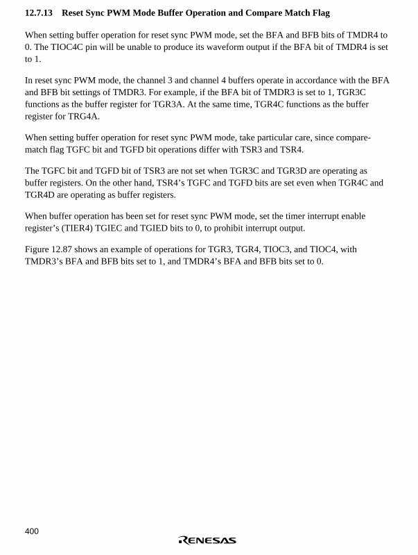
400
12.7.13 Reset Sync PWM Mode Buffer Operation and Compare Match Flag
When setting buffer operation for reset sync PWM mode, set the BFA and BFB bits of TMDR4 to0. The TIOC4C pin will be unable to produce its waveform output if the BFA bit of TMDR4 is setto 1.
In reset sync PWM mode, the channel 3 and channel 4 buffers operate in accordance with the BFAand BFB bit settings of TMDR3. For example, if the BFA bit of TMDR3 is set to 1, TGR3Cfunctions as the buffer register for TGR3A. At the same time, TGR4C functions as the bufferregister for TRG4A.
When setting buffer operation for reset sync PWM mode, take particular care, since compare-match flag TGFC bit and TGFD bit operations differ with TSR3 and TSR4.
The TGFC bit and TGFD bit of TSR3 are not set when TGR3C and TGR3D are operating asbuffer registers. On the other hand, TSR4’s TGFC and TGFD bits are set even when TGR4C andTGR4D are operating as buffer registers.
When buffer operation has been set for reset sync PWM mode, set the timer interrupt enableregister’s (TIER4) TGIEC and TGIED bits to 0, to prohibit interrupt output.
Figure 12.87 shows an example of operations for TGR3, TGR4, TIOC3, and TIOC4, withTMDR3’s BFA and BFB bits set to 1, and TMDR4’s BFA and BFB bits set to 0.

401
TGR3A
TGR3C
TGR3B, TGR4A,TGR4B
TGR3D, TGR4C,TGR4D
H'0000
TIOC3ATIOC3B
TIOC3D
TIOC4A
TIOC4C
TIOC4BTIOC4D
TGF3C
TGF3D
TGF4C
TGF4D
TGR3A,TGR3C
TGR3B, TGR3D, TGR4A, TGR4C,
TGR4B, TGR4D
Buffer transfer with compare match A3TCNT3
Not setNot setSet
Set
Point a
Point b
Figure 12.87 Buffer Operation and Compare-Match Flags in Reset Sync PWM Mode
• A mask operation
For A mask, the above operation is modified as follows:
When setting buffer operation for reset sync PWM mode, set the BFA and BFB bits ofTMDR4 to 0. The TIOC4C pin will be unable to produce its waveform output if the BFA bit ofTMDR4 is set to 1.
In reset sync PWM mode, the channel 3 and channel 4 buffers operate in accordance with theBFA and BFB bit settings of TMDR3. For example, if the BFA bit of TMDR3 is set to 1,TGR3C functions as the buffer register for TGR3A. At the same time, TGR4C functions as thebuffer register for TRG4A.
When setting buffer operation for reset sync PWM mode, the compare-match flag TGFC bit and TGFD bit operations will be the same for TSR3 and TSR4.
The TGFC bit and TGFD bit of TSR3 are not set when TGR3C and TGR3D are operating asbuffer registers. The TGFC bit and TGFD bit of TSR4 are not set when TGR4C and TGR4D are operating as buffer registers.

402
When setting the buffer operation in the reset synchronous PWM mode , it is not necessary to set the timer interrupt enable register’s (TIER4) TGIEC and TGIED bits to 0, to prohibit interrupt output.
Figure 12.88 shows an example of operations for TGR3, TGR4, TIOC3, and TIOC4, withTMDR3’s BFA and BFB bits set to 1, and TMDR4’s BFA and BFB bits set to 0.
TGR3A
TGR3C
TGR3B,TGR4ATGR4B
TGR3D,TGR4CTGR4D
H'0000
TIOC3A
TIOC3B
TIOC3D
TIOC4A
TIOC4C
TIOC4B
TIOC4D
TGF3C
TGF3D
TGF4C
TGF4D
TCNT3
TGR3A,TGR3C
TGR3B,TGR3DTGR4A,TGR4CTGR4B,TGR4D
Not set
Not set
Not set
Buffer transfer with compare match A3
Point a
Point b
Not set
Figure 12.88 Buffer Operation and Compare-Match Flags in Reset Sync PWM Mode(for A Mask)
12.7.14 Overflow Flags in Reset Sync PWM Mode
When set to reset sync PWM mode, TCNT3 and TCNT4 start counting when the CST3 bit ofTSTR is set to 1. At this point, TCNT4’s count clock source and count edge obey the TCR3setting.
In reset sync PWM mode, with cycle register TGR3A’s set value at H'FFFF, take care whenspecifying TGR3A compare-match for the counter clear source, since the operation of theoverflow flag (TCFV bit) differs with TSR3 and TSR4.

403
When TCNT3 and TCNT4 count up to H'FFFF, a compare-match occurs with TGR3A, andTCNT3 and TCNT4 are both cleared. At this point, TSR3’s TCFV bit is not set, but the TCFV bitof TSR4 is set.
This can be avoided by sync setting for channel 3 and channel 4. Set the SYNC3 and SYNC4 bitsof the timer sync register (TSYR) to 1, compare-match with TGR3A by TCR3 for the counterclear source, and sync clear with TCR4. This gives the sync setting for channels 3 and 4.
Figure 12.89 shows a TCFV bit operation example in reset sync PWM mode with a set value forcycle register TGR3A of H'FFFF, when a TGR3A compare-match has been specified withoutsynchronous setting for the counter clear source.
TGR3A(H'FFFF)
H'0000
TCF3V
TCF4V
TCNT3 = TCNT4
Counter cleared by compare match A3
Not set
Set
Figure 12.89 Reset Sync PWM Mode Overflow Flag
• A mask operation
For A mask, the above operation is modified as follows:
When set to reset sync PWM mode, TCNT3 and TCNT4 start counting when the CST3 bit ofTSTR is set to 1. At this point, TCNT4’s count clock source and count edge obey the TCR3setting.
In reset sync PWM mode, with cycle register TGR3A’s set value at H'FFFF and specifyingTGR3A compare-match for the counter clear source, the operation of the overflow flag TCFV bit for both TSR3 and TSR4 will be the same.
When TCNT3 and TCNT4 count up to H'FFFF, a compare-match occurs with TGR3A, andTCNT3 and TCNT4 are both cleared. At this point, TCFV bits for TSR3 and TSR4 are not set.
Figure 12.90 shows a TCFV bit operation example in reset sync PWM mode with a set valuefor cycle register TGR3A of H'FFFF, when a TGR3A compare-match has been specifiedwithout synchronous setting for the counter clear source.

404
TGR3A(H'FFFF)
H'0000
TCF3V
TCF4V
TCNT3=TCNT4
Not set
Not set
Counter clear by compare match 3A
Figure. 12.90 Reset Sync PWM Mode Overflow Flag (for A Mask)

405
12.7.15 Notes on Compare Match Flags in Complementary PWM Mode
In complementary PWM mode, buffer register compare-match flags can be set only for comparewith three counters (TCNT3, TCNT4, and TCNTS).
Note that when the buffer register set value is dead time (Td), 2Td, TGR3A – Td, orTGR3A – 2Td, the buffer register compare-match flag may not be set.
Figure 12.91 gives a description when TGR3B is the specified duty setting register, TGR3D thebuffer register with TGR3A – Td as the buffer register set value.
TGR3A
TCDR(TGR3A –
Td)
TGR3B
TDDR
H'0000
TIOC3A
TIOC3B
TIOC3D
TGF3Bsetting
signal
TGF3Dsettingsignal
TCNT3
TGR3D
TCNT4
TGR3B,TGR3D
Point a Point b Point c Point d
Point a: TGR3D setting TdPoint b: TGR3D setting TGR3A – Td or TGR3A – 2TDPoint c: TGR3D setting Td or 2TdPoint d: TGR3D setting TGR3A – Td or TGR3A – 2Td, and the setting signal is not output
Figure 12.91 Special Properties of Compare Match Flag in Complementary PWM Mode

406
• A mask operation
For A mask, the above operation is modified as follows:
In complementary PWM mode, buffer register compare-match flags can be set only forcompare with three counters (TCNT3, TCNT4, and TCNTS).
Special properties of compare match flag disappear and compare match flags of buffer registers are set to all set values of buffer registers.
Figure 12.92 shows an example when setting the duty setting register to TGR3B, bufferregister to TGR3D and Buffer register to TGR3A-Td.
TGR3A
TCDR(TGR3A -Td)
TGR3B
TDDR
H'0000
TIOC3A
TIOC3B
TIOC3D
Point a Point b Point c Point d
TGF3B setting signal
TGF3D setting signal
TCNT3
TGR3D
TCNT4
TGR3B,TGR3D
Set signals are output when:Point a: TGR3D setting is TdPoint b: TGR3D settings are TGR3A-Td, TGR3A-2TdPoint c: TGR3D settings are Td, 2TdPoint d: TGR3D settings are TGR3A-Td, TGR3A-2Td
Figure. 12.92 Special Properties of Compare Match Flag in Complementary PWM Mode(for A Mask)

407
12.7.16 Contention between Overflow/Underflow and Counter Clearing
If overflow/underflow and counter clearing occur simultaneously, the TCFV/TCFU flag in TSR isnot set and TCNT clearing takes precedence.
Figure 12.93 shows the operation timing when a TGR compare-match is specified as the clearingsource, and H'FFFF is set in TGR.
φ
TCNT inputclock
TCNT
Counter clear signal
TGF flag
TCFV flag
H'FFFF H'0000
Disabled
Figure 12.93 Contention between Overflow and Counter Clearing

408
12.7.17 Contention between TCNT Write and Overflow/Underflow
If there is an up-count or down-count in the T2 state of a TCNT write cycle, andoverflow/underflow occurs, the TCNT write takes precedence and the TCFV/TCFU flag in TSR isnot set .
Figure 12.94 shows the operation timing in this case.
φ
Address
Write signal
TCNT inputclock
TCNT
TCFV flag
H'FFFF N TCNT write data
Disabled
TCNT write cycle
T1 T2
TCNT address
Figure 12.94 Contention between TCNT Write and Overflow

409
12.7.18 Cautions on Transition from Normal Operation or PWM Mode 1 to Reset-
Synchronous PWM Mode
When making a transition from channel 3 or 4 normal operation or PWM mode 1 to reset-synchronous PWM mode, if the counter is halted with the output pins (TIOC3B, TIOC3D,TIOC4A, TIOC4C, TIOC4B, TIOC4D) in the high-impedance state, followed by the transition toreset-synchronous PWM mode and operation in that mode, the initial pin output will not becorrect.
When making a transition from normal operation to reset-synchronous PWM mode, write H'11 toregisters TIOR3H, TIOR3L, TIOR4H, and TIOR4L to initialize the output pins to low leveloutput, then set an initial register value of H'00 before making the mode transition.
When making a transition from PWM mode 1 to reset-synchronous PWM mode, first switch tonormal operation, then initialize the output pins to low level output and set an initial register valueof H'00 before making the transition to reset-synchronous PWM mode.
12.7.19 Output Level in Complementary PWM Mode and Reset-Synchronous PWM Mode
When channels 3 and 4 are in complementary PWM mode or reset-synchronous PWM mode, thePWM waveform output level is set with the OLSP and OLSN bits in the timer output controlregister (TOCR). In the case of complementary PWM mode or reset-synchronous PWM mode,TIOR should be set to H'00.
12.7.20 Cautions on Using the Chopping Function in Complementary PWM Mode or Reset
Synchronous PWM Mode (A Mask Excluded)
When channels 3 and 4 are in complementary PWM mode or reset-synchronous PWM mode andusing the chopping output function, setting the PWM waveform output level to low active with theOLSP and OLSN bits in the timer output control register (TOCR) will output an incorrect gatesignal or chopping output.
When channels 3 and 4 are in complementary PWM mode or reset-synchronous PWM mode andusing the chopping output function, the PWM output level should be set to high active.
12.7.21 Cautions on Carrying Out Buffer Operation of Channel 0 in PWM Mode (A Mask
Excluded)
In PWM mode 1, the TGRA and TGRB registers are used in pairs and PWM waveform is outputto the TIOCA pin. In the same manner, the TGRC and TGRD registers are used in pairs and PWMwaveform is output to the TIOCC pin. If either the TGRC or TGRD register is operating as abuffer register, the TIOCC pin cannot execute default output setting or PWM waveform outputwith the I/O control register (TIOR).

410
Note that for channel 0, the TIOCC pin allows both default output setting by TIOR and PWMoutput when setting buffer operation only for the TGRD register in PWM mode.
When using channel 0 in PWM mode 1 and setting buffer operation, use both the TGRC andTGRD registers as buffer registers.
12.7.22 Cautions on Restarting with Sync Clear of Another Channel in Complementary
PWM Mode (A Mask Excluded)
The complementation PWM mode operates while waiting for the current, next and the followingset values as values of the PWM duty. If clearing sync from another channel during operation, thePWM output will return to the default output and restart.
When restarting with sync clear, the following operations may occur:
1. When restarting with sync clear, the next set value is used for the PWM duty, however, thefollowing set value may be used by mistake.
2. If sync clear and the setting of the value following the next value of PWM duty (write toTGR4D) occurs at the same time, the next set value may be overwritten.
How to avoid 1
When selecting the mode to transfer using the crest/trough in the complementary PWM transfermode, set the value following the next value of the PWM duty (write to TGR4D) while thetemporary register is not executing comparisons. Furthermore, set the occurrence timing of syncclear while the temporary register is not executing comparisons.
When selecting the mode to transfer using the crest in the transfer mode, set the value followingthe next value of the PWM duty (write to TGR4D) while the temporary register is not executingcomparisons and while TCNT3 and TCNT4 are counting up. Furthermore, set the occurrencetiming of sync clear while the temporary register is not executing comparisons and while TCNT3and TCNT4 are counting up.
When selecting the mode to transfer using the trough in the transfer mode, set the value followingthe next value of the PWM duty (write to TGR4D) while the temporary register is not executingcomparisons and while TCNT3 and TCNT4 are counting down. Furthermore, set the occurrencetiming of sync clear while the temporary register is not executing comparisons and while TCNT3and TCNT4 are counting down.
How to avoid 2
Regardless of the transfer mode, set so that the sync clear and the setting of the value followingthe next value (write to TGR4D) does not occur at the same time.

411
Figure 12.95 shows an example of the duration while the temporary register is executingcomparisons. initial TB, TA, and TB indicate the duration of the temporary register comparison.
initial TB TA TB TA TB
TGR3A
TCDR
TDDR
H'0000
TCNT3
TCNT4
Figure. 12.95 Temporary Register Comparison Execution Time
12.8 MTU Output Pin Initialization
12.8.1 Operating Modes
The MTU has the following six operating modes. Waveform output is possible in all of thesemodes.
• Normal mode (channels 0 and 4)
• PWM mode 1 (channels 0 and 4)
• PWM mode 2 (channels 0 and 2)
• Phase counting modes 1–4 (channels 1 and 2)
• Complementary PWM mode (channels 3 and 4)
• Reset-synchronous PWM mode (channels 3 and 4)
The MTU output pin initialization method for each of these modes is described in this section.
12.8.2 Reset Start Operation
The MTU output pins (TIOC*) are initialized low by a reset and in standby mode. Since MTU pinfunction selection is performed by the pin function controller (PFC), when the PFC is set, theMTU pin states at that point are output to the ports. When MTU output is selected by the PFCimmediately after a reset, the MTU output initial level, low, is output directly at the port. Whenthe active level is low, the system will operate at this point, and therefore the PFC setting shouldbe made after initialization of the MTU output pins is completed.
Note: Channel number and port notation are substituted for *.

412
12.8.3 Operation in Case of Re-Setting Due to Error During Operation, Etc.
If an error occurs during MTU operation, MTU output should be cut by the system. Cutoff isperformed by switching the pin output to port output with the PFC and outputting the inverse ofthe active level. For large-current pins, output can also be cut by hardware, using port outputenable (POE). The pin initialization procedures for re-setting due to an error during operation, etc.,and the procedures for restarting in a different mode after re-setting, are shown below.
The MTU has six operating modes, as stated above. There are thus 36 mode transitioncombinations, but some transitions are not available with certain channel and mode combinations.Possible mode transition combinations are shown in table 12.18.
Table 12.18 Mode Transition Combinations
After
Before Normal PWM1 PWM2 PCM CPWM RPWM
Normal (1) (2) (3) (4) (5) (6)
PWM1 (7) (8) (9) (10) (11) (12)
PWM2 (13) (14) (15) (16) None None
PCM (17) (18) (19) (20) None None
CPWM (21) (22) None None (23) (24)
RPWM (25) (26) None None (27) (28)
Legend:Normal: Normal modePWM1: PWM mode 1PWM2: PWM mode 2PCM: Phase counting modes 1–4CPWM: Complementary PWM modeRPWM: Reset-synchronous PWM mode
The above abbreviations are used in some places in following descriptions.
12.8.4 Overview of Initialization Procedures and Mode Transitions in Case of Error
during Operation, Etc.
• When making a transition to a mode (Normal, PWM1, PWM2, PCM) in which the pin outputlevel is selected by the timer I/O control register (TIOR) setting, initialize the pins by means ofa TIOR setting.
• In PWM mode 1, since a waveform is not output to the TIOC*B (TIOC *D) pin, setting TIORwill not initialize the pins. If initialization is required, carry it out in normal mode, then switchto PWM mode 1.

413
• In PWM mode 2, since a waveform is not output to the cycle register pin, setting TIOR willnot initialize the pins. If initialization is required, carry it out in normal mode, then switch toPWM mode 2.
• In normal mode or PWM mode 2, if TGRC and TGRD operate as buffer registers, settingTIOR will not initialize the buffer register pins. If initialization is required, clear buffer mode,carry out initialization, then set buffer mode again.
• In PWM mode 1, if either TGRC or TGRD operates as a buffer register, setting TIOR will notinitialize the TGRC pin. To initialize the TGRC pin, clear buffer mode, carry out initialization,then set buffer mode again.
• When making a transition to a mode (CPWM, RPWM) in which the pin output level is selectedby the timer output control register (TOCR) setting, switch to normal mode and performinitialization with TIOR, then restore TIOR to its initial value, and temporarily disable channel3 and 4 output with the timer output master enable register (TOER). Then operate the unit inaccordance with the mode setting procedure (TOCR setting, TMDR setting, TOER setting).
Pin initialization procedures are described below for the numbered combinations in table 12.19.The active level is assumed to be low.
Note: Channel number is substituted for * indicated in this article.

414
(1) Operation when Error Occurs during Normal Mode Operation, and Operation isRestarted in Normal Mode: Figure 12.96 shows an explanatory diagram of the case where anerror occurs in normal mode and operation is restarted in normal mode after re-setting.
1RESET
2TMDR
(normal)
3TOER
(1)
5PFC
(MTU)
4TIOR(1 init0 out)
6TSTR
(1)
7Match
8Error
occurs
9PFC
(PORT)
10TSTR
(0)
11TMDR
(normal)
12TIOR(1 init0 out)
13PFC
(MTU)
14TSTR
(1)
MTU output
TIOC*A
TIOC*B
Port output
PEn
PEn
n=0 to 15
High-Z
High-Z
Figure 12.96 Error Occurrence in Normal Mode, Recovery in Normal Mode
1. After a reset, MTU output is low and ports are in the high-impedance state.
2. After a reset, the TMDR setting is for normal mode.
3. For channels 3 and 4, enable output with TOER before initializing the pins with TIOR.
4. Initialize the pins with TIOR. (The example shows initial high output, with low output oncompare-match occurrence.)
5. Set MTU output with the PFC.
6. The count operation is started by TSTR.
7. Output goes low on compare-match occurrence.
8. An error occurs.
9. Set port output with the PFC and output the inverse of the active level.
10. The count operation is stopped by TSTR.
11. Not necessary when restarting in normal mode.
12. Initialize the pins with TIOR.
13. Set MTU output with the PFC.
14. Operation is restarted by TSTR.

415
(2) Operation when Error Occurs during Normal Mode Operation, and Operation isRestarted in PWM Mode 1: Figure 12.97 shows an explanatory diagram of the case where anerror occurs in normal mode and operation is restarted in PWM mode 1 after re-setting.
1RESET
2TMDR
(normal)
3TOER
(1)
5PFC
(MTU)
4TIOR(1 init0 out)
6TSTR
(1)
7Match
8Error occurs
9PFC
(PORT)
10TSTR
(0)
11TMDR
(PWM1)
12TIOR(1 init0 out)
13PFC
(MTU)
14TSTR
(1)
MTU output
TIOC*A
TIOC*B
Port output
PEn
PEn
• Not initialized (TIOC*B)
n=0 to 15
High-Z
High-Z
Figure 12.97 Error Occurrence in Normal Mode, Recovery in PWM Mode 1
1 to 10 are the same as in figure 12.96.
11. Set PWM mode 1.
12. Initialize the pins with TIOR. (In PWM mode 1, the TIOC*B side is not initialized. Ifinitialization is required, initialize in normal mode, then switch to PWM mode 1.)
13. Set MTU output with the PFC.
14. Operation is restarted by TSTR.

416
(3) Operation when Error Occurs during Normal Mode Operation, and Operation isRestarted in PWM Mode 2: Figure 12.98 shows an explanatory diagram of the case where anerror occurs in normal mode and operation is restarted in PWM mode 2 after re-setting.
1RESET
2TMDR
(normal)
3TOER
(1)
5PFC
(MTU)
4TIOR(1 init0 out)
6TSTR
(1)
7Match
8Error occurs
9PFC
(PORT)
10TSTR
(0)
11TMDR
(PWM2)
12TIOR(1 init0 out)
13PFC
(MTU)
14TSTR
(1)
MTU output
TIOC*A
TIOC*B
Port output
PEn
PEn
• Not initialized (cycle register)
n=0 to 15
High-Z
High-Z
Figure 12.98 Error Occurrence in Normal Mode, Recovery in PWM Mode 2
1 to 10 are the same as in figure 12.96.
11. Set PWM mode 2.
12. Initialize the pins with TIOR. (In PWM mode 2, the cycle register pins are not initialized. Ifinitialization is required, initialize in normal mode, then switch to PWM mode 2.)
13. Set MTU output with the PFC.
14. Operation is restarted by TSTR.
Note: PWM mode 2 can only be set for channels 0–2, and therefore TOER setting is notnecessary.

417
(4) Operation when Error Occurs during Normal Mode Operation, and Operation isRestarted in Phase Counting Mode: Figure 12.99 shows an explanatory diagram of the casewhere an error occurs in normal mode and operation is restarted in phase counting mode after re-setting.
1RESET
2TMDR
(normal)
3TOER
(1)
5PFC
(MTU)
4TIOR(1 init0 out)
6TSTR
(1)
7Match
8Error occurs
9PFC
(PORT)
10TSTR
(0)
11TMDR(PCM)
12TIOR(1 init0 out)
13PFC
(MTU)
14TSTR
(1)
MTU output
TIOC*A
TIOC*B
Port output
PEn
PEn
n=0 to 15
High-Z
High-Z
Figure 12.99 Error Occurrence in Normal Mode, Recovery in Phase Counting Mode
1 to 10 are the same as in figure 12.96.
11. Set phase counting mode.
12. Initialize the pins with TIOR.
13. Set MTU output with the PFC.
14. Operation is restarted by TSTR.
Note: Phase counting mode can only be set for channels 1 and 2, and therefore TOER setting isnot necessary.

418
(5) Operation when Error Occurs during Normal Mode Operation, and Operation isRestarted in Complementary PWM Mode: Figure 12.100 shows an explanatory diagram of thecase where an error occurs in normal mode and operation is restarted in complementary PWMmode after re-setting.
1RESET
2TMDR
(normal)
3TOER
(1)
5PFC
(MTU)
4TIOR(1 init0 out)
6TSTR
(1)
7Match
8Error occurs
9PFC
(PORT)
10TSTR
(0)
11TIOR(0 init0 out)
12TIOR
(disabled)
13TOER
(0)
14TOCR
15TMDR
(CPWM)
(16)TOER
(1)
(17)PFC
(MTU)
(18)TSTR
(1)
MTU output
TIOC3A
TIOC3B
TIOC3D
Port output
PE9
PE8
PE11 High-Z
High-Z
High-Z
Figure 12.100 Error Occurrence in Normal Mode, Recovery in Complementary PWMMode
1 to 10 are the same as in figure 12.96.
11. Initialize the normal mode waveform generation section with TIOR.
12. Disable operation of the normal mode waveform generation section with TIOR.
13. Disable channel 3 and 4 output with TOER.
14. Select the complementary PWM output level and cyclic output enabling/disabling withTOCR.
15. Set complementary PWM.
16. Enable channel 3 and 4 output with TOER.
17. Set MTU output with the PFC.
18. Operation is restarted by TSTR.

419
(6) Operation when Error Occurs during Normal Mode Operation, and Operation isRestarted in Reset-Synchronous PWM Mode: Figure 12.101 shows an explanatory diagram ofthe case where an error occurs in normal mode and operation is restarted in reset-synchronousPWM mode after re-setting.
1RESET
2TMDR
(normal)
3TOER
(1)
5PFC
(MTU)
4TIOR(1 init0 out)
6TSTR
(1)
7Match
8Error occurs
9PFC
(PORT)
10TSTR
(0)
11TIOR(0 init0 out)
12TIOR
(disabled)
13TOER
(0)
14TOCR
15TMDR
(CPWM)
16TOER
(1)
17PFC
(MTU)
18TSTR
(1)
MTU output
TIOC3A
TIOC3B
TIOC3D
Port output
PE9
PE8
PE11 High-Z
High-Z
High-Z
Figure 12.101 Error Occurrence in Normal Mode, Recovery in Reset-SynchronousPWM Mode
1 to 13 are the same as in figure 12.100.
14. Select the reset-synchronous PWM output level and cyclic output enabling/disabling withTOCR.
15. Set reset-synchronous PWM.
16. Enable channel 3 and 4 output with TOER.
17. Set MTU output with the PFC.
18. Operation is restarted by TSTR.

420
(7) Operation when Error Occurs during PWM Mode 1 Operation, and Operation isRestarted in Normal Mode: Figure 12.102 shows an explanatory diagram of the case where anerror occurs in PWM mode 1 and operation is restarted in normal mode after re-setting.
1RESET
2TMDR
(PWM1)
3TOER
(1)
5PFC
(MTU)
4TIOR(1 init0 out)
6TSTR
(1)
7Match
8Error occurs
9PFC
(PORT)
10TSTR
(0)
11TMDR
(normal)
12TIOR(1 init0 out)
13PFC
(MTU)
14TSTR
(1)
MTU output
TIOC*A
TIOC*B
Port output
PEn
PEn
• Not initialized (TIOC*B)
n=0 to 15
High-Z
High-Z
Figure 12.102 Error Occurrence in PWM Mode 1, Recovery in Normal Mode
1. After a reset, MTU output is low and ports are in the high-impedance state.
2. Set PWM mode 1.
3. For channels 3 and 4, enable output with TOER before initializing the pins with TIOR.
4. Initialize the pins with TIOR. (The example shows initial high output, with low output oncompare-match occurrence. In PWM mode 1, the TIOC*B side is not initialized.)
5. Set MTU output with the PFC.
6. The count operation is started by TSTR.
7. Output goes low on compare-match occurrence.
8. An error occurs.
9. Set port output with the PFC and output the inverse of the active level.
10. The count operation is stopped by TSTR.
11. Set normal mode.
12. Initialize the pins with TIOR.
13. Set MTU output with the PFC.
14. Operation is restarted by TSTR.

421
(8) Operation when Error Occurs during PWM Mode 1 Operation, and Operation isRestarted in PWM Mode 1: Figure 12.103 shows an explanatory diagram of the case where anerror occurs in PWM mode 1 and operation is restarted in PWM mode 1 after re-setting.
1RESET
2TMDR
(PWM1)
3TOER
(1)
5PFC
(MTU)
4TIOR(1 init0 out)
6TSTR
(1)
7Match
8Error occurs
9PFC
(PORT)
10TSTR
(0)
11TMDR
(PWM1)
12TIOR(1 init0 out)
13PFC
(MTU)
14TSTR
(1)
MTU output
TIOC*A
TIOC*B
Port output
PEn
PEn
• Not initialized (TIOC*B) • Not initialized (TIOC*B)
n=0 to 15
High-Z
High-Z
Figure 12.103 Error Occurrence in PWM Mode 1, Recovery in PWM Mode 1
1 to 10 are the same as in figure 12.102.
11. Not necessary when restarting in PWM mode 1.
12. Initialize the pins with TIOR. (In PWM mode 1, the TIOC*B side is not initialized.)
13. Set MTU output with the PFC.
14. Operation is restarted by TSTR.

422
(9) Operation when Rrror Occurs during PWM Mode 1 Operation, and Operation isRestarted in PWM Mode 2: Figure 12.104 shows an explanatory diagram of the case where anerror occurs in PWM mode 1 and operation is restarted in PWM mode 2 after re-setting.
1RESET
2TMDR
(PWM1)
3TOER
(1)
5PFC
(MTU)
4TIOR(1 init0 out)
6TSTR
(1)
7Match
8Error occurs
9PFC
(PORT)
10TSTR
(0)
11TMDR
(PWM2)
12TIOR(1 init0 out)
13PFC
(MTU)
14TSTR
(1)
MTU output
TIOC*A
TIOC*B
Port output
PEn
PEn
• Not initialized (TIOC*B)
• Not initialized (cycle register)
n=0 to 15
High-Z
High-Z
Figure 12.104 Error Occurrence in PWM Mode 1, Recovery in PWM Mode 2
1 to 10 are the same as in figure 12.102.
11. Set PWM mode 2.
12. Initialize the pins with TIOR. (In PWM mode 2, the cycle register pins are not initialized.)
13. Set MTU output with the PFC.
14. Operation is restarted by TSTR.
Note: PWM mode 2 can only be set for channels 0–2, and therefore TOER setting is notnecessary.

423
(10) Operation when Error Occurs during PWM Mode 1 Operation, and Operation isRestarted in Phase Counting Mode: Figure 12.105 shows an explanatory diagram of the casewhere an error occurs in PWM mode 1 and operation is restarted in phase counting mode after re-setting.
1RESET
2TMDR
(PWM1)
3TOER
(1)
5PFC
(MTU)
4TIOR(1 init0 out)
6TSTR
(1)
7Match
8Error occurs
9PFC
(PORT)
10TSTR
(0)
11TMDR(PCM)
12TIOR(1 init0 out)
13PFC
(MTU)
14TSTR
(1)
MTU output
TIOC*A
TIOC*B
Port output
PEn
PEn
• Not initialized (TIOC*B)
n=0 to 15
High-Z
High-Z
Figure 12.105 Error Occurrence in PWM Mode 1, Recovery in Phase Counting Mode
1 to 10 are the same as in figure 12.102.
11. Set phase counting mode.
12. Initialize the pins with TIOR.
13. Set MTU output with the PFC.
14. Operation is restarted by TSTR.
Note: Phase counting mode can only be set for channels 1 and 2, and therefore TOER setting isnot necessary.

424
(11) Operation when Error Occurs during PWM Mode 1 Operation, and Operation isRestarted in Complementary PWM Mode: Figure 12.106 shows an explanatory diagram of thecase where an error occurs in PWM mode 1 and operation is restarted in complementary PWMmode after re-setting.
1RESET
2TMDR
(PWM1)
3TOER
(1)
5PFC
(MTU)
4TIOR(1 init0 out)
6TSTR
(1)
7Match
8Error occurs
9PFC
(PORT)
10TSTR
(0)
11TMDR
(normal)
12TIOR(0 init0 out)
13TIOR
(disabled)
14TOER
(0)
15TOCR
16TMDR
(CPWM)
17TOER
(1)
18PFC
(MTU)
19TSTR
(1)
MTU output
TIOC3A
TIOC3B
TIOC3D
Port output
PE9
PE8
PE11
• Not initialized (TIOC3B)
• Not initialized (TIOC3D)
High-Z
High-Z
High-Z
Figure 12.106 Error Occurrence in PWM Mode 1, Recovery in ComplementaryPWM Mode
1 to 10 are the same as in figure 12.102.
11. Set normal mode for initialization of the normal mode waveform generation section.
12. Initialize the PWM mode 1 waveform generation section with TIOR.
13. Disable operation of the PWM mode 1 waveform generation section with TIOR.
14. Disable channel 3 and 4 output with TOER.
15. Select the complementary PWM output level and cyclic output enabling/disabling withTOCR.
16. Set complementary PWM.
17. Enable channel 3 and 4 output with TOER.
18. Set MTU output with the PFC.
19. Operation is restarted by TSTR.

425
(12) Operation when Error Occurs during PWM Mode 1 Operation, and Operation isRestarted in Reset-Synchronous PWM Mode: Figure 12.107 shows an explanatory diagram ofthe case where an error occurs in PWM mode 1 and operation is restarted in reset-synchronousPWM mode after re-setting.
1RESET
2TMDR
(PWM1)
3TOER
(1)
5PFC
(MTU)
4TIOR(1 init0 out)
6TSTR
(1)
7Match
8Error occurs
9PFC
(PORT)
10TSTR
(0)
11TMDR
(normal)
12TIOR(0 init0 out)
13TIOR
(disabled)
14TOER
(0)
15TOCR
16TMDR
(RPWM)
17TOER
(1)
18PFC
(MTU)
19TSTR
(1)
MTU output
TIOC3A
TIOC3B
TIOC3D
Port output
PE9
PE8
PE11
• Not initialized (TIOC3B)
• Not initialized (TIOC3D)
High-Z
High-Z
High-Z
Figure 12.107 Error Occurrence in PWM Mode 1, Recovery in Reset-SynchronousPWM Mode
1 to 14 are the same as in figure 12.106.
15. Select the reset-synchronous PWM output level and cyclic output enabling/disabling withTOCR.
16. Set reset-synchronous PWM.
17. Enable channel 3 and 4 output with TOER.
18. Set MTU output with the PFC.
19. Operation is restarted by TSTR.

426
(13) Operation when Error Occurs during PWM Mode 2 Operation, and Operation isRestarted in Normal Mode: Figure 12.108 shows an explanatory diagram of the case where anerror occurs in PWM mode 2 and operation is restarted in normal mode after re-setting.
1RESET
2TMDR
(PWM2)
3TIOR(1 init0 out)
5TSTR
(1)
4PFC
(MTU)
6Match
7Error occurs
8PFC
(PORT)
9TSTR
(0)
10TMDR
(normal)
11TIOR(1 init0 out)
12PFC
(MTU)
13TSTR
(1)
MTU output
TIOC*A
TIOC*B
Port output
PEn
PEn
• Not initialized (cycle register)
n=0 to 15
High-Z
High-Z
Figure 12.108 Error Occurrence in PWM Mode 2, Recovery in Normal Mode
1. After a reset, MTU output is low and ports are in the high-impedance state.
2. Set PWM mode 2.
3. Initialize the pins with TIOR. (The example shows initial high output, with low output oncompare-match occurrence. In PWM mode 2, the cycle register pins are not initialized. In theexample, TIOC *A is the cycle register.)
4. Set MTU output with the PFC.
5. The count operation is started by TSTR.
6. Output goes low on compare-match occurrence.
7. An error occurs.
8. Set port output with the PFC and output the inverse of the active level.
9. The count operation is stopped by TSTR.
10. Set normal mode.
11. Initialize the pins with TIOR.
12. Set MTU output with the PFC.
13. Operation is restarted by TSTR.

427
(14) Operation when Error Occurs during PWM Mode 2 Operation, and Operation isRestarted in PWM Mode 1: Figure 12.109 shows an explanatory diagram of the case where anerror occurs in PWM mode 2 and operation is restarted in PWM mode 1 after re-setting.
1RESET
2TMDR
(PWM2)
3TIOR(1 init0 out)
5TSTR
(1)
4PFC
(MTU)
6Match
7Error occurs
8PFC
(PORT)
9TSTR
(0)
10TMDR
(PWM1)
11TIOR(1 init0 out)
12PFC
(MTU)
13TSTR
(1)
MTU output
TIOC*A
TIOC*B
Port output
PEn
PEn
• Not initialized (TIOC*B)
• Not initialized (cycle register)
n=0 to 15
High-Z
High-Z
Figure 12.109 Error Occurrence in PWM Mode 2, Recovery in PWM Mode 1
1 to 9 are the same as in figure 12.108.
10. Set PWM mode 1.
11. Initialize the pins with TIOR. (In PWM mode 1, the TIOC*B side is not initialized.)
12. Set MTU output with the PFC.
13. Operation is restarted by TSTR.

428
(15) Operation when Error Occurs during PWM Mode 2 Operation, and Operation isRestarted in PWM Mode 2: Figure 12.110 shows an explanatory diagram of the case where anerror occurs in PWM mode 2 and operation is restarted in PWM mode 2 after re-setting.
1RESET
2TMDR
(PWM2)
3TIOR(1 init0 out)
5TSTR
(1)
4PFC
(MTU)
6Match
7Error occurs
8PFC
(PORT)
9TSTR
(0)
10TMDR
(PWM2)
11TIOR(1 init0 out)
12PFC
(MTU)
13TSTR
(1)
MTU output
TIOC*A
TIOC*B
Port output
PEn
PEn
• Not initialized (cycle register) • Not initialized (cycle register)
n=0 to 15
High-Z
High-Z
Figure 12.110 Error Occurrence in PWM Mode 2, Recovery in PWM Mode 2
1 to 9 are the same as in figure 12.108.
10. Not necessary when restarting in PWM mode 2.
11. Initialize the pins with TIOR. (In PWM mode 2, the cycle register pins are not initialized.)
12. Set MTU output with the PFC.
13. Operation is restarted by TSTR.

429
(16) Operation when Error Occurs during PWM Mode 2 Operation, and Operation isRestarted in Phase Counting Mode: Figure 12.111 shows an explanatory diagram of the casewhere an error occurs in PWM mode 2 and operation is restarted in phase counting mode after re-setting.
1RESET
2TMDR
(PWM2)
3TIOR(1 init0 out)
5TSTR
(1)
4PFC
(MTU)
6Match
7Error occurs
8PFC
(PORT)
9TSTR
(0)
10TMDR(PCM)
11TIOR(1 init0 out)
12PFC
(MTU)
13TSTR
(1)
MTU output
TIOC*A
TIOC*B
Port output
PEn
PEn
• Not initialized (cycle register)
n=0 to 15
High-Z
High-Z
Figure 12.111 Error Occurrence in PWM Mode 2, Recovery in Phase Counting Mode
1 to 9 are the same as in figure 12.108.
10. Set phase counting mode.
11. Initialize the pins with TIOR.
12. Set MTU output with the PFC.
13. Operation is restarted by TSTR.
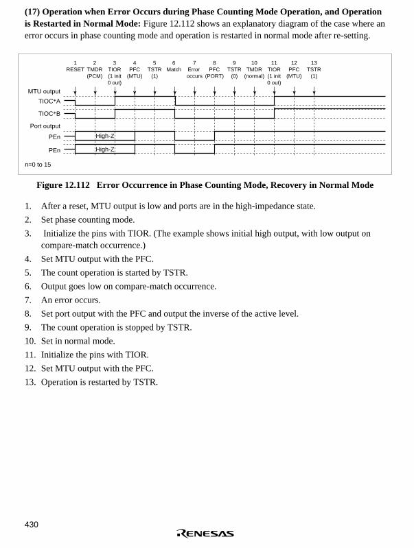
430
(17) Operation when Error Occurs during Phase Counting Mode Operation, and Operationis Restarted in Normal Mode: Figure 12.112 shows an explanatory diagram of the case where anerror occurs in phase counting mode and operation is restarted in normal mode after re-setting.
1RESET
2TMDR(PCM)
3TIOR(1 init0 out)
5TSTR
(1)
4PFC
(MTU)
6Match
7Error occurs
8PFC
(PORT)
9TSTR
(0)
10TMDR
(normal)
11TIOR(1 init0 out)
12PFC
(MTU)
13TSTR
(1)
MTU output
TIOC*A
TIOC*B
Port output
PEn
PEn
n=0 to 15
High-Z
High-Z
Figure 12.112 Error Occurrence in Phase Counting Mode, Recovery in Normal Mode
1. After a reset, MTU output is low and ports are in the high-impedance state.
2. Set phase counting mode.
3. Initialize the pins with TIOR. (The example shows initial high output, with low output oncompare-match occurrence.)
4. Set MTU output with the PFC.
5. The count operation is started by TSTR.
6. Output goes low on compare-match occurrence.
7. An error occurs.
8. Set port output with the PFC and output the inverse of the active level.
9. The count operation is stopped by TSTR.
10. Set in normal mode.
11. Initialize the pins with TIOR.
12. Set MTU output with the PFC.
13. Operation is restarted by TSTR.

431
(18) Operation when Error Occurs during Phase Counting Mode Operation, and Operationis Restarted in PWM Mode 1: Figure 12.113 shows an explanatory diagram of the case where anerror occurs in phase counting mode and operation is restarted in PWM mode 1 after re-setting.
1RESET
2TMDR(PCM)
3TIOR(1 init0 out)
5TSTR
(1)
4PFC
(MTU)
6Match
7Error occurs
8PFC
(PORT)
9TSTR
(0)
10TMDR
(PWM1)
11TIOR(1 init0 out)
12PFC
(MTU)
13TSTR
(1)
MTU output
TIOC*A
TIOC*B
Port output
PEn
PEn
• Not initialized (TIOC*B)
n=0 to 15
High-Z
High-Z
Figure 12.113 Error Occurrence in Phase Counting Mode, Recovery in PWM Mode 1
1 to 9 are the same as in figure 12.112.
10. Set PWM mode 1.
11. Initialize the pins with TIOR. (In PWM mode 1, the TIOC *B side is not initialized.)
12. Set MTU output with the PFC.
13. Operation is restarted by TSTR.

432
(19) Operation when Error Occurs during Phase Counting Mode Operation, and Operationis Restarted in PWM Mode 2: Figure 12.114 shows an explanatory diagram of the case where anerror occurs in phase counting mode and operation is restarted in PWM mode 2 after re-setting.
1RESET
2TMDR(PCM)
3TIOR(1 init0 out)
5TSTR
(1)
4PFC
(MTU)
6Match
7Error occurs
8PFC
(PORT)
9TSTR
(0)
10TMDR
(PWM2)
11TIOR(1 init0 out)
12PFC
(MTU)
13TSTR
(1)
MTU output
TIOC*A
TIOC*B
Port output
PEn
PEn
n=0 to 15
High-Z
High-Z
• Not initialized (cycle register)
Figure 12.114 Error Occurrence in Phase Counting Mode, Recovery in PWM Mode 2
1 to 9 are the same as in figure 12.112.
10. Set PWM mode 2.
11. Initialize the pins with TIOR. (In PWM mode 2, the cycle register pins are not initialized.)
12. Set MTU output with the PFC.
13. Operation is restarted by TSTR.

433
(20) Operation when Error Occurs during Phase Counting Mode Operation, and Operationis Restarted in Phase Counting Mode: Figure 12.115 shows an explanatory diagram of the casewhere an error occurs in phase counting mode and operation is restarted in phase counting modeafter re-setting.
1RESET
2TMDR(PCM)
3TIOR(1 init0 out)
5TSTR
(1)
4PFC
(MTU)
6Match
7Error occurs
8PFC
(PORT)
9TSTR
(0)
10TMDR(PCM)
11TIOR(1 init0 out)
12PFC
(MTU)
13TSTR
(1)
MTU output
TIOC*A
TIOC*B
Port output
PEn
PEn
n=0 to 15
High-Z
High-Z
Figure 12.115 Error Occurrence in Phase Counting Mode, Recovery in PhaseCounting Mode
1 to 9 are the same as in figure 12.112.
10. Not necessary when restarting in phase counting mode.
11. Initialize the pins with TIOR.
12. Set MTU output with the PFC.
13. Operation is restarted by TSTR.

434
(21) Operation when Error Occurs during Complementary PWM Mode Operation, andOperation is Restarted in Normal Mode: Figure 12.116 shows an explanatory diagram of thecase where an error occurs in complementary PWM mode and operation is restarted in normalmode after re-setting.
1RESET
2TOCR
3TMDR
(CPWM)
5PFC
(MTU)
4TOER
(1)
6TSTR
(1)
7Match
8 Error occurs
9PFC
(PORT)
10TSTR
(0)
11TMDR
(normal)
12TIOR(1 init0 out)
13PFC
(MTU)
14TSTR
(1)
MTU output
TIOC3A
TIOC3B
TIOC3D
Port output
PE9
PE8
PE11
High-Z
High-Z
High-Z
Figure 12.116 Error Occurrence in Complementary PWM Mode, Recovery inNormal Mode
1. After a reset, MTU output is low and ports are in the high-impedance state.
2. Select the complementary PWM output level and cyclic output enabling/disabling withTOCR.
3. Set complementary PWM.
4. Enable channel 3 and 4 output with TOER.
5. Set MTU output with the PFC.
6. The count operation is started by TSTR.
7. The complementary PWM waveform is output on compare-match occurrence.
8. An error occurs.
9. Set port output with the PFC and output the inverse of the active level.
10. The count operation is stopped by TSTR. (MTU output becomes the complementary PWMoutput initial value.)
11. Set normal mode. (MTU output goes low.)
12. Initialize the pins with TIOR.
13. Set MTU output with the PFC.
14. Operation is restarted by TSTR.

435
(22) Operation when Error Occurs during Complementary PWM Mode Operation, andOperation is Restarted in PWM Mode 1: Figure 12.117 shows an explanatory diagram of thecase where an error occurs in complementary PWM mode and operation is restarted in PWMmode 1 after re-setting.
1RESET
2TOCR
3TMDR
(CPWM)
5PFC
(MTU)
4TOER
(1)
6TSTR
(1)
7Match
8Error occurs
9PFC
(PORT)
10TSTR
(0)
11TMDR
(PWM1)
12TIOR(1 init0 out)
13PFC
(MTU)
14TSTR
(1)
MTU output
TIOC3A
TIOC3B
TIOC3D
Port output
PE9
PE8
PE11
• Not initialized (TIOC3B)
• Not initialized (TIOC3D)
High-Z
High-Z
High-Z
Figure 12.117 Error Occurrence in Complementary PWM Mode, Recovery in PWMMode 1
1 to 10 are the same as in figure 12.116.
11. Set PWM mode 1. (MTU output goes low.)
12. Initialize the pins with TIOR. (In PWM mode 1, the TIOC *B side is not initialized.)
13. Set MTU output with the PFC.
14. Operation is restarted by TSTR.

436
(23a) Operation when Error Occurs during Complementary PWM Mode Operation, andOperation is Restarted in Complementary PWM Mode: Figure 12.118 shows an explanatorydiagram of the case where an error occurs in complementary PWM mode and operation isrestarted in complementary PWM mode after re-setting (when operation is restarted using thecycle and duty settings at the time the counter was stopped).
1RESET
2TOCR
3TMDR
(CPWM)
5PFC
(MTU)
4TOER
(1)
6TSTR
(1)
7Match
8Error occurs
9PFC
(PORT)
10TSTR
(0)
11PFC
(MTU)
12TSTR
(1)
13Match
MTU output
TIOC3A
TIOC3B
TIOC3D
Port output
PE9
PE8
PE11
High-Z
High-Z
High-Z
Figure 12.118 Error Occurrence in Complementary PWM Mode, Recovery inComplementary PWM Mode
1 to 10 are the same as in figure 12.116.
11. Set MTU output with the PFC.
12. Operation is restarted by TSTR.
13. The complementary PWM waveform is output on compare-match occurrence.
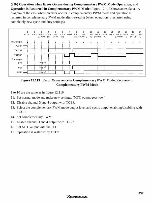
437
(23b) Operation when Error Occurs during Complementary PWM Mode Operation, andOperation is Restarted in Complementary PWM Mode: Figure 12.119 shows an explanatorydiagram of the case where an error occurs in complementary PWM mode and operation isrestarted in complementary PWM mode after re-setting (when operation is restarted usingcompletely new cycle and duty settings).
1RESET
2TOCR
3TMDR
(CPWM)
5PFC
(MTU)
4TOER
(1)
6TSTR
(1)
7Match
8Error occurs
9PFC
(PORT)
10TSTR
(0)
11TMDR
(normal)
12TOER
(0)
13TOCR
14TMDR
(CPWM)
15TOER
(1)
16PFC
(MTU)
17TSTR
(1)
MTU output
TIOC3A
TIOC3B
TIOC3D
Port output
PE9
PE8
PE11
High-Z
High-Z
High-Z
Figure 12.119 Error Occurrence in Complementary PWM Mode, Recovery inComplementary PWM Mode
1 to 10 are the same as in figure 12.116.
11. Set normal mode and make new settings. (MTU output goes low.)
12. Disable channel 3 and 4 output with TOER.
13. Select the complementary PWM mode output level and cyclic output enabling/disabling withTOCR.
14. Set complementary PWM.
15. Enable channel 3 and 4 output with TOER.
16. Set MTU output with the PFC.
17. Operation is restarted by TSTR.

438
(24) Operation when Error Occurs during Complementary PWM Mode Operation, andOperation is Restarted in Reset-Synchronous PWM Mode: Figure 12.120 shows anexplanatory diagram of the case where an error occurs in complementary PWM mode andoperation is restarted in reset-synchronous PWM mode.
1RESET
2TOCR
3TMDR
(CPWM)
5PFC
(MTU)
4TOER
(1)
6TSTR
(1)
7Match
8Error occurs
9PFC
(PORT)
10TSTR
(0)
11TMDR
(normal)
12TOER
(0)
13TOCR
14TMDR
(RPWM)
15TOER
(1)
16PFC
(MTU)
17TSTR
(1)
MTU output
TIOC3A
TIOC3B
TIOC3D
Port output
PE9
PE8
PE11
High-Z
High-Z
High-Z
Figure 12.120 Error Occurrence in Complementary PWM Mode,Recovery in Reset-Synchronous PWM Mode
1 to 10 are the same as in figure 12.116.
11. Set normal mode. (MTU output goes low.)
12. Disable channel 3 and 4 output with TOER.
13. Select the reset-synchronous PWM mode output level and cyclic output enabling/disablingwith TOCR.
14. Set reset-synchronous PWM.
15. Enable channel 3 and 4 output with TOER.
16. Set MTU output with the PFC.
17. Operation is restarted by TSTR.
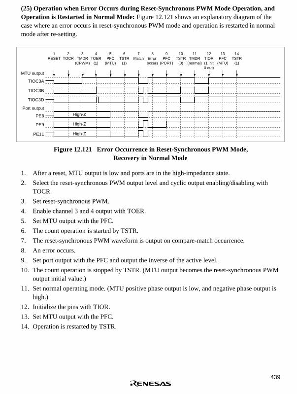
439
(25) Operation when Error Occurs during Reset-Synchronous PWM Mode Operation, andOperation is Restarted in Normal Mode: Figure 12.121 shows an explanatory diagram of thecase where an error occurs in reset-synchronous PWM mode and operation is restarted in normalmode after re-setting.
1RESET
2TOCR
3TMDR
(CPWM)
5PFC
(MTU)
4TOER
(1)
6TSTR
(1)
7Match
8Error occurs
9PFC
(PORT)
10TSTR
(0)
11TMDR
(normal)
12TIOR(1 init0 out)
13PFC
(MTU)
14TSTR
(1)
MTU output
TIOC3A
TIOC3B
TIOC3D
Port output
PE9
PE8
PE11
High-Z
High-Z
High-Z
Figure 12.121 Error Occurrence in Reset-Synchronous PWM Mode,Recovery in Normal Mode
1. After a reset, MTU output is low and ports are in the high-impedance state.
2. Select the reset-synchronous PWM output level and cyclic output enabling/disabling withTOCR.
3. Set reset-synchronous PWM.
4. Enable channel 3 and 4 output with TOER.
5. Set MTU output with the PFC.
6. The count operation is started by TSTR.
7. The reset-synchronous PWM waveform is output on compare-match occurrence.
8. An error occurs.
9. Set port output with the PFC and output the inverse of the active level.
10. The count operation is stopped by TSTR. (MTU output becomes the reset-synchronous PWMoutput initial value.)
11. Set normal operating mode. (MTU positive phase output is low, and negative phase output ishigh.)
12. Initialize the pins with TIOR.
13. Set MTU output with the PFC.
14. Operation is restarted by TSTR.

440
(26) Operation when Error Occurs during Reset-Synchronous PWM Mode Operation, andOperation is Restarted in PWM Mode 1: Figure 12.122 shows an explanatory diagram of thecase where an error occurs in reset-synchronous PWM mode and operation is restarted in PWMmode 1 after re-setting.
1RESET
2TOCR
3TMDR
(RPWM)
5PFC
(MTU)
4TOER
(1)
6TSTR
(1)
7Match
8Error occurs
9PFC
(PORT)
10TSTR
(0)
11TMDR
(PWM1)
12TIOR(1 init0 out)
13PFC
(MTU)
14TSTR
(1)
MTU output
TIOC3A
TIOC3B
TIOC3D
Port output
PE9
PE8
PE11
• Not initialized (TIOC3B)
• Not initialized (TIOC3D)
High-Z
High-Z
High-Z
Figure 12.122 Error Occurrence in Reset-Synchronous PWM Mode,Recovery in PWM Mode 1
1 to 10 are the same as in figure 12.121.
11. Set PWM mode 1. (MTU positive phase output is low, and negative phase output is high.)
12. Initialize the pins with TIOR. (In PWM mode 1, the TIOC *B side is not initialized.)
13. Set MTU output with the PFC.
14. Operation is restarted by TSTR.

441
(27) Operation when Error Occurs during Reset-Synchronous PWM Mode Operation, andOperation is Restarted in Complementary PWM Mode: Figure 12.123 shows an explanatorydiagram of the case where an error occurs in reset-synchronous PWM mode and operation isrestarted in complementary PWM mode after re-setting.
1RESET
2TOCR
3TMDR
(RPWM)
5PFC
(MTU)
4TOER
(1)
6TSTR
(1)
7Match
8Error occurs
9PFC
(PORT)
10TSTR
(0)
11TOER
(0)
12TOCR
13TMDR
(CPWM)
14TOER
(1)
15PFC
(MTU)
16TSTR
(1)
MTU output
TIOC3A
TIOC3B
TIOC3D
Port output
PE9
PE8
PE11
High-Z
High-Z
High-Z
Figure 12.123 Error Occurrence in Reset-Synchronous PWM Mode,Recovery in Complementary PWM Mode
1 to 10 are the same as in figure 12.121.
11. Disable channel 3 and 4 output with TOER.
12. Select the complementary PWM output level and cyclic output enabling/disabling withTOCR.
13. Set complementary PWM. (The MTU cyclic output pin goes low.)
14. Enable channel 3 and 4 output with TOER.
15. Set MTU output with the PFC.
16. Operation is restarted by TSTR.

442
(28) Operation when Error Occurs during Reset-Synchronous PWM Mode Operation, andOperation is Restarted in Reset-Synchronous PWM Mode: Figure 12.124 shows anexplanatory diagram of the case where an error occurs in reset-synchronous PWM mode andoperation is restarted in reset-synchronous PWM mode after re-setting.
1RESET
2TOCR
3TMDR
(RPWM)
5PFC
(MTU)
4TOER
(1)
6TSTR
(1)
7Match
8Error occurs
9PFC
(PORT)
10TSTR
(0)
11PFC
(MTU)
12TSTR
(1)
13Match
MTU output
TIOC3A
TIOC3B
TIOC3D
Port output
PE9
PE8
PE11
High-Z
High-Z
High-Z
High-Z
High-Z
High-Z
Figure 12.124 Error Occurrence in Reset-Synchronous PWM Mode,Recovery in Reset-Synchronous PWM Mode
1 to 10 are the same as in figure 12.121.
11. Set MTU output with the PFC.
12. Operation is restarted by TSTR.
13. The reset-synchronous PWM waveform is output on compare-match occurrence.

443
12.9 Port Output Enable (POE)
The port output enable (POE) can be used to establish a high-impedance state for high-currentpins, by changing the POE0–POE3 pin input, depending on the output status of the high-currentpins (PE09/TIOC3B, PE11/TIOC3D, PE12/TIOC4A, PE13/TIOC4B/MRES,PE14/TIOC4C/DACK0/AH, PE15/TIOC4D/DACK1/IRQOUT). It can also simultaneouslygenerate interrupt requests.
The high-current pins also become high-impedance regardless of whether these pin functions areselected in cases such as when the oscillator stops or in standby mode. Refer to section 4, ClockPulse Generator (CPG), for details.
12.9.1 Features
• Each of the POE0–POE3 input pins can be set for falling edge, φ/8 × 16, φ/16 × 16, or φ/128 ×16 low-level sampling.
• High-current pins can be set to high-impedance state by POE0–POE3 pin falling-edge or low-level sampling.
• High-current pins can be set to high-impedance state when the high-current pin output levelsare compared and simultaneous low-level output continues for one cycle or more (except in the33.3 MHz version).
• Interrupts can be generated by input-level sampling or output-level comparison results.

444
12.9.2 Block Diagram
The POE has input-level detection circuitry and output-level detection circuitry, as shown in theblock diagram of figure 12.125.
TIOC3B*
TIOC3D*
TIOC4A*
TIOC4C*
TIOC4B*
TIOC4D*
POE3POE2POE1POE0
Output level detection circuit
Output level detection circuit
Output level detection circuit
Input level detection circuit
Falling-edgedetection circuit
Low-leveldetection circuit
OCSR
ICSR
φ/8 φ/16 φ/128
High-impedance request controlsignal
Interruptrequest
Note: * Includes multiplexed pins.
Figure 12.125 POE Block Diagram

445
12.9.3 Pin Configuration
Table 12.18 shows the POE pins.
Table 12.18 Pin Configuration
Name Abbreviation I/O Description
Port output enable input pins POE0–POE3 Input Input request signals to make high-current pins high-impedance state
Table 12.19 shows output-level comparisons with pin combinations.
Table 12.19 Output Level Comparisons
Pin Combination I/O Description
PE09/TIOC3B andPE11/TIOC3D
Output All high-current pins are made high-impedancestate when the pins simultaneously output low-levelfor longer than 1 cycle.
PE12/TIOC4A andPE14/TIOC4C/DACK0/AH
Output All high-current pins are made high-impedancestate when the pins simultaneously output low-levelfor longer than 1 cycle.
PE13/TIOC4B/MRES andPE15/TIOC4D/DACK1/IRQOUT
Output All high-current pins are made high-impedancestate when the pins simultaneously output low-levelfor longer than 1 cycle.
12.9.4 Register Configuration
The POE has the two registers shown in table 12.20. The input level control/status register (ICSR)controls both POE0–POE3 pin input signal detection and interrupts. The output levelcontrol/status register (OCSR) controls both the enable/disable of output comparison andinterrupts.
Table 12.20 Input Level Control/Status Register Configuration
Name Abbreviation R/W Initial Value Address Access Size
Input level control/statusregister
ICSR R/(W)* 1 H'0000 H'FFFF83C0H'FFFF83C1
8, 16, 32
Output levelcontrol/status register
OCSR R/(W)* 2 H'0000 H'FFFF83C2H'FFFF83C3
8, 16, 32
Notes: * 1 Only 0 writes to bits 15–12 are possible to clear the flags.* 2 Only 0 writes to bits 15 are possible to clear the flags.

446
12.10 POE Register Descriptions
12.10.1 Input Level Control/Status Register (ICSR)
The input level control/status register (ICSR) is a 16-bit read/write register that selects the POE0–POE3 pin input modes, controls the enable/prohibit of interrupts, and indicates status. If any of thePOE3F–POE0F bits are set to 1, the high current pins become high impedance state.
ICSR is initialized to H'0000 by power-on resets; however, it is not initialized for manual resets,standby mode, or sleep mode, so the previous data is maintained.
Bit: 15 14 13 12 11 10 9 8
POE3F POE2F POE1F POE0F — — — PIE
Initial value: 0 0 0 0 0 0 0 0
R/W: R/(W)* R/(W)* R/(W)* R/(W)* R R R R/W
Bit: 7 6 5 4 3 2 1 0
POE3M1 POE3M0 POE2M1 POE2M0 POE1M1 POE1M0 POE0M1 POE0M0
Initial value: 0 0 0 0 0 0 0 0
R/W: R/W R/W R/W R/W R/W R/W R/W R/W
Note: * Only 0 writes are possible to clear the flags.
• Bit 15—POE3 Flag (POE3F): This flag indicates that a high impedance request has been inputto the POE3 pin.
Bit 15: POE3F Description
0 Clear condition: By writing 0 to POE3F after reading a POE3F = 1(initial value)
1 Set condition: When the input set by ICSR bits 7 and 6 occurs atthe POE3 pin
• Bit 14—POE2 Flag (POE2F): This flag indicates that a high impedance request has been inputto the POE2 pin.
Bit 14: POE2F Description
0 Clear condition: By writing 0 to POE2F after reading a POE2F = 1(initial value)
1 Set condition: When the input set by ICSR bits 5 and 4 occurs atthe POE2 pin

447
• Bit 13—POE1 Flag (POE1F): This flag indicates that a high impedance request has been inputto the POE1 pin.
Bit 13: POE1F Description
0 Clear condition: By writing 0 to POE1F after reading a POE1F = 1(initial value)
1 Set condition: When the input set by ICSR bits 3 and 2 occurs atthe POE1 pin
• Bit 12—POE0 Flag (POE0F): This flag indicates that a high impedance request has been inputto the POE0 pin.
Bit 12: POE0F Description
0 Clear condition: By writing 0 to POE0F after reading a POE0F = 1(initial value)
1 Set condition: When the input set by ICSR bits 1 and 0 occurs atthe POE0 pin
• Bits 11–9—Reserved: These bits always read as 0. The write value should always be 0.
• Bit 8—Port Interrupt Enable (PIE): Enables or disables interrupt requests when any of thePOE0F–POE3F bits of the ICSR are set to 1.
Bit 8: PIE Description
0 Interrupt requests disabled (initial value)
1 Interrupt requests enabled
• Bits 7 and 6—POE3 Mode 1, 0 (POE3M1 and POE3M0): These bits select the input mode ofthe POE3 pin.
Bit 7:POE3M1
Bit 6:POE3M0 Description
0 0 Accept request on falling edge of POE3 input. (initial value)
1 Accept request when POE3 input has been sampled for 16φ/8 clock pulses, and all are low level.
1 0 Accept request when POE3 input has been sampled for 16φ/16 clock pulses, and all are low level.
1 Accept request when POE3 input has been sampled for 16φ/128 clock pulses, and all are low level.

448
• Bits 5 and 4—POE2 Mode 1, 0 (POE2M1 and POE2M0): These bits select the input mode ofthe POE2 pin.
Bit 5:POE2M1
Bit 4:POE2M0 Description
0 0 Accept request on falling edge of POE2 input. (initial value)
1 Accept request when POE2 input has been sampled for 16φ/8 clock pulses, and all are low level.
1 0 Accept request when POE2 input has been sampled for 16φ/16 clock pulses, and all are low level.
1 Accept request when POE2 input has been sampled for 16φ/128 clock pulses, and all are low level.
• Bits 3 and 2—POE1 Mode 1, 0 (POE1M1 and POE1M0): These bits select the input mode ofthe POE1 pin.
Bit 3:POE1M1
Bit 2:POE1M0 Description
0 0 Accept request on falling edge of POE1 input. (initial value)
1 Accept request when POE1 input has been sampled for 16φ/8 clock pulses, and all are low level.
1 0 Accept request when POE1 input has been sampled for 16φ/16 clock pulses, and all are low level.
1 Accept request when POE1 input has been sampled for 16φ/128 clock pulses, and all are low level.
• Bits 1 and 0—POE0 Mode 1, 0 (POE0M1 and POE0M0): These bits select the input mode ofthe POE0 pin.
Bit 1:POE0M1
Bit 0:POE0M0 Description
0 0 Accept request on falling edge of POE0 input. (initial value)
1 Accept request when POE0 input has been sampled for 16φ/8 clock pulses, and all are low level.
1 0 Accept request when POE0 input has been sampled for 16φ/16 clock pulses, and all are low level.
1 Accept request when POE0 input has been sampled for 16φ/128 clock pulses, and all are low level.

449
12.10.2 Output Level Control/Status Register (OCSR)
The output level control/status register (OCSR) is a 16-bit read/write register that controls theenable/disable of both output level comparison and interrupts, and indicates status. If the OSF bitis set to 1, the high current pins become high impedance.
OCSR is initialized to H'0000 by an external power-on reset; however, it is not initialized formanual resets, reset by WDT standby mode, or sleep mode, so the previous data is maintained.
Bit: 15 14 13 12 11 10 9 8
OSF — — — — — OCE OIE
Initial value: 0 0 0 0 0 0 0 0
R/W: R/(W)* R R R R R R/W R/W
Bit: 7 6 5 4 3 2 1 0
— — — — — — — —
Initial value: 0 0 0 0 0 0 0 0
R/W: R R R R R R R R
Note: * Only 0 writes are possible to clear the flag.
• Bit 15—Output Short Flag (OSF): This flag indicates that among the three pairs of 2 phaseoutputs compared, the outputs of at least one pair have simultaneously become Low leveloutput.
Bit 15: OSF Description
0 Clear condition: By writing 0 to OSF after reading an OSF = 1 (initial value)
1 Set condition: When any one pair of the 2-phase outputs simultaneouslybecome Low level
• Bits 14–10—Reserved: These bits always read as 0. The write value should always be 0.

450
• Bit 9—Output Level Compare Enable (OCE): This bit enables the start of output levelcomparisons. When setting this bit, pay special attention to the output pin combinations shownin table 12.19. When 0 is output, the OSF bit is set to 1 at the same time this bit is set, andoutput goes to high impedance. Accordingly, bits 15–11 and bit 9 of the port E data register(PEDR) are set to 1. For the MTU output comparison, set the bit to 1 after setting the MTU’soutput pins with the PFC. Set this bit only when using pins as outputs.
When the OCE bit is set to 1, if OIE = 0 a high-impedance request will not be issued even ifOSF is set to 1. Therefore, in order to have a high-impedance request issued according to theresult of the output comparison, the OIE bit must be set to 1. When OCE = 1 and OIE = 1, aninterrupt request will be generated at the same time as the high-impedance request; however,this interrupt can be masked by means of an interrupt controller (INTC) setting.
Bit 9: OCE Description
0 Output level compare disabled (initial value)
1 Output level compare enabled; makes an output high impedance requestwhen OSF = 1.
• Bit 8—Output Short Interrupt Enable (OIE): Makes interrupt requests when the OSF bit of theOCSR is set.
Bit 8: OIE Description
0 Interrupt requests disabled (initial value)
1 Interrupt requests enabled
• Bits 7–0—Reserved: Always read as 0, and cannot be modified.

451
12.11 Operation
12.11.1 Input Level Detection Operation
If the input conditions set by the ICSR occur on any of the POE pins, all high-current pins becomehigh-impedance state.
Falling Edge Detection: When a change from high to low level is input to the POE pins.
Low-Level Detection: Figure 12.126 shows the low-level detection operation. Sixteen continuouslow levels are sampled with the sampling clock established by the ICSR. If even one high level isdetected during this interval, the low level is not accepted.
CK
Samplingclock
3
POE input
PE9/TIOC3B
When low level is sampled at all points
When high level is sampledat least once
Flag set (POE received)
Flag not set
High-impedancestate*
Note: * Other large-current pins (PE11/TIOC3D, PE12/TIOC4A, PE13/TIOC4B/MRES, PE14/TIOC4C/DACK0/AH, PE15/TIOC4D/DACK1/IROOUT) also go to the high-impedance state at the same time.
21
21
16
13
8/16/128 clockcycles
Figure 12.126 Low-Level Detection Operation

452
12.11.2 Output-Level Compare Operation
Figure 12.127 shows an example of the output-level compare operation for the combination ofPE09/TIOC3B and PE11/TIOC3D. The operation is the same for the other pin combinations.
CK
PE11/TIOC3D
PE09/TIOC3B
0 level overlapping detected
High impedance state
Figure 12.127 Output-Level Detection Operation
12.11.3 Release from High-Impedance State
High-current pins that have entered high-impedance state due to input-level detection can bereleased either by returning them to their initial state with a power-on reset, or by clearing all ofthe bit 12–15 (POE0F–POE3F) flags of the ICSR. High-current pins that have become high-impedance due to output-level detection can be released either by returning them to their initialstate with a power-on reset, or by first clearing bit 9 (OCE) of the OCSR to disable output-levelcompares, then clearing the bit 15 (OSF) flag. However, when returning from high-impedancestate by clearing the OSF flag, always do so only after outputting a high level from the high-current pins (TIOC3B, TIOC3D, TIOC4A, TIOC4B, TIOC4C, and TIOC4D). High-level outputscan be achieved by setting the MTU internal registers. See section 12.2, MTU RegisterDescriptions, for details.

453
12.11.4 POE timing
Figure 12.128 shows an example of timing from POE input to high impedance of pin.
POE input
CK last transition
CK
PE9/TIOC3B
Last transition edge detected
High impedance state*
Note: * Other high current pins (PE11/TICO3D, PE12/TIOC4A, PE13/TIOC4B/MRES, PE14/TIOC4C/DACK0/AH, PE15/TIOC4D/DACK1/IRQOUT) will enter the highimpedance state with the same timing.
Figure 12.128 Last Transition Edge Detection Operation
12.11.5 Usage Notes
To perform POE level detection, first set POE input to high level.

454

455
Section 13 Watchdog Timer (WDT)
13.1 Overview
The watchdog timer (WDT) is a 1-channel timer for monitoring system operations. If a systemencounters a problem (crashes, for example) and the timer counter overflows without beingrewritten correctly by the CPU, an overflow signal (WDTOVF) is output externally. The WDTcan simultaneously generate an internal reset signal for the entire chip.
When the watchdog function is not needed, the WDT can be used as an interval timer. In theinterval timer operation, an interval timer interrupt is generated at each counter overflow. TheWDT is also used in recovering from the standby mode.
13.1.1 Features
• Works in watchdog timer mode or interval timer mode.
• Outputs WDTOVF in the watchdog timer mode. When the counter overflows in the watchdogtimer mode, overflow signal WDTOVF is output externally. You can select whether to resetthe chip internally when this happens. Either the power-on reset or manual reset signal can beselected as the internal reset signal.
• Generates interrupts in the interval timer mode. When the counter overflows, it generates aninterval timer interrupt.
• Clears standby mode.
• Works with eight counter input clocks.

456
13.1.2 Block Diagram
Figure 13.1 is the block diagram of the WDT.
φ/2φ/64φ/128φ/256φ/512φ/1024φ/4096φ/8192
Internalclock sources
Clock
Overflow
Clockselect
Interruptcontrol
Resetcontrol
RSTCSR
TCSR:TCNT:
RSTCSR:
Timer control/status registerTimer counterReset control/status register
TCNT TCSR
Module busBus
interface Inte
rnal
dat
a bu
s
ITI(interrupt
signal)
WDTOVFInternal
reset signal*
WDT
Note: * The internal reset signal can be generated by setting the register.The type of reset can be selected (power-on or manual).
Figure 13.1 WDT Block Diagram
13.1.3 Pin Configuration
Table 13.1 shows the pin configuration.
Table 13.1 Pin Configuration
Pin Abbreviation I/O Function
Watchdog timer overflow WDTOVF O Outputs the counter overflow signal in thewatchdog timer mode
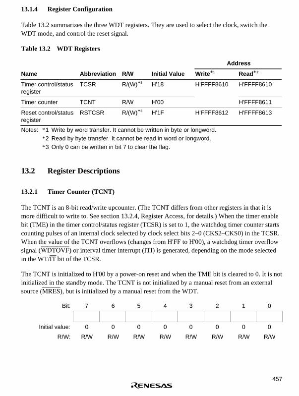
457
13.1.4 Register Configuration
Table 13.2 summarizes the three WDT registers. They are used to select the clock, switch theWDT mode, and control the reset signal.
Table 13.2 WDT Registers
Address
Name Abbreviation R/W Initial Value Write * 1 Read* 2
Timer control/statusregister
TCSR R/(W)* 3 H'18 H'FFFF8610 H'FFFF8610
Timer counter TCNT R/W H'00 H'FFFF8611
Reset control/statusregister
RSTCSR R/(W)* 3 H'1F H'FFFF8612 H'FFFF8613
Notes: * 1 Write by word transfer. It cannot be written in byte or longword.* 2 Read by byte transfer. It cannot be read in word or longword.* 3 Only 0 can be written in bit 7 to clear the flag.
13.2 Register Descriptions
13.2.1 Timer Counter (TCNT)
The TCNT is an 8-bit read/write upcounter. (The TCNT differs from other registers in that it ismore difficult to write to. See section 13.2.4, Register Access, for details.) When the timer enablebit (TME) in the timer control/status register (TCSR) is set to 1, the watchdog timer counter startscounting pulses of an internal clock selected by clock select bits 2–0 (CKS2–CKS0) in the TCSR.When the value of the TCNT overflows (changes from H'FF to H'00), a watchdog timer overflowsignal (WDTOVF) or interval timer interrupt (ITI) is generated, depending on the mode selectedin the WT/IT bit of the TCSR.
The TCNT is initialized to H'00 by a power-on reset and when the TME bit is cleared to 0. It is notinitialized in the standby mode. The TCNT is not initialized by a manual reset from an externalsource (MRES), but is initialized by a manual reset from the WDT.
Bit: 7 6 5 4 3 2 1 0
Initial value: 0 0 0 0 0 0 0 0
R/W: R/W R/W R/W R/W R/W R/W R/W R/W

458
13.2.2 Timer Control/Status Register (TCSR)
The timer control/status register (TCSR) is an 8-bit read/write register. (The TCSR differs fromother registers in that it is more difficult to write to. See section 13.2.4, Register Access, fordetails.) Its functions include selecting the timer mode and clock source.
Bits 7–5 are initialized to 000 by a power-on reset or in standby mode. Bits 2–0 are initialized to000 by a power-on reset, but retain their values in the standby mode. These bits are not initializedby a manual reset from an external source (MRES), but are initialized by a manual reset from theWDT.
Bit: 7 6 5 4 3 2 1 0
OVF WT/IT TME — — CKS2 CKS1 CKS0
Initial value: 0 0 0 1 1 0 0 0
R/W: R/(W) R/W R/W R R R/W R/W R/W
• Bit 7—Overflow Flag (OVF): Indicates that the TCNT has overflowed from H'FF to H'00 inthe interval timer mode. It is not set in the watchdog timer mode.
Bit 7: OVF Description
0 No overflow of TCNT in interval timer mode (initial value)
Cleared by reading OVF, then writing 0 in OVF
1 TCNT overflow in the interval timer mode
• Bit 6—Timer Mode Select (WT/IT): Selects whether to use the WDT as a watchdog timer orinterval timer. When the TCNT overflows, the WDT either generates an interval timerinterrupt (ITI) or generates a WDTOVF signal, depending on the mode selected.
Bit 6: WT/ IT Description
0 Interval timer mode: interval timer interrupt request to the CPU whenTCNT overflows (initial value)
1 Watchdog timer mode: WDTOVF signal output externally when TCNToverflows. (Section 13.2.3, Reset Control/Status Register (RSTCSR),describes in detail what happens when TCNT overflows in the watchdogtimer mode.)

459
• Bit 5—Timer Enable (TME): Enables or disables the timer.
Bit 5: TME Description
0 Timer disabled: TCNT is initialized to H'00 and count-up stops (initialvalue)
1 Timer enabled: TCNT starts counting. A WDTOVF signal or interrupt isgenerated when TCNT overflows.
• Bits 4 and 3—Reserved: These bits always read as 1. The write value should always be 1.
• Bits 2–0: Clock Select 2–0 (CKS2–CKS0): These bits select one of eight internal clock sourcesfor input to the TCNT. The clock signals are obtained by dividing the frequency of the systemclock (φ).
Description
Bit 2: CKS2 Bit 1: CKS1 Bit 0: CKS0 Clock SourceOverflow Interval *
(φ = 28.7 MHz)
0 0 0 φ/2 (initial value) 17.9 µs
0 0 1 φ/64 573.4 µs
0 1 0 φ/128 1.1 ms
0 1 1 φ/256 2.3 ms
1 0 0 φ/512 4.6 ms
1 0 1 φ/1024 9.2 ms
1 1 0 φ/4096 36.7 ms
1 1 1 φ/8192 73.4 ms
Note: * The overflow interval listed is the time from when the TCNT begins counting at H'00 untilan overflow occurs.

460
13.2.3 Reset Control/Status Register (RSTCSR)
The RSTCSR is an 8-bit readable and writable register. (The RSTCSR differs from other registersin that it is more difficult to write. See section 13.2.4, Register Access, for details.) It controlsoutput of the internal reset signal generated by timer counter (TCNT) overflow and selects theinternal reset signal type. RSTCR is initialized to H'1F by input of a reset signal from the RES pin,but is not initialized by the internal reset signal generated by the overflow of the WDT. It isinitialized to H'1F in standby mode.
Bit: 7 6 5 4 3 2 1 0
WOVF RSTE RSTS — — — — —
Initial value: 0 0 0 1 1 1 1 1
R/W: R/(W)* R/W R/W R R R R R
Note: * Only 0 can be written in bit 7 to clear the flag.
• Bit 7—Watchdog Timer Overflow Flag (WOVF): Indicates that the TCNT has overflowed(H'FF–H'00) in the watchdog timer mode. It is not set in the interval timer mode.
Bit 7: WOVF Description
0 No TCNT overflow in watchdog timer mode (initial value)
Cleared when software reads WOVF, then writes 0 in WOVF
1 Set by TCNT overflow in watchdog timer mode
• Bit 6—Reset Enable (RSTE): Selects whether to reset the chip internally if the TCNToverflows in the watchdog timer mode.
Bit 6: RSTE Description
0 Not reset when TCNT overflows (initial value). LSI not reset internally,but TCNT and TCSR reset within WDT.
1 Reset when TCNT overflows
• Bit 5—Reset Select (RSTS): Selects the type of internal reset generated if the TCNT overflowsin the watchdog timer mode.
Bit 5: RSTS Description
0 Power-on reset (initial value)
1 Manual reset
• Bits 4–0—Reserved: These bits always read as 1. The write value should always be 1.
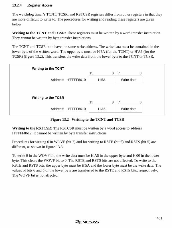
461
13.2.4 Register Access
The watchdog timer’s TCNT, TCSR, and RSTCSR registers differ from other registers in that theyare more difficult to write to. The procedures for writing and reading these registers are givenbelow.
Writing to the TCNT and TCSR: These registers must be written by a word transfer instruction.They cannot be written by byte transfer instructions.
The TCNT and TCSR both have the same write address. The write data must be contained in thelower byte of the written word. The upper byte must be H'5A (for the TCNT) or H'A5 (for theTCSR) (figure 13.2). This transfers the write data from the lower byte to the TCNT or TCSR.
H'5AH'FFFF8610Address:
Writing to the TCNT15 8 7 0
Write data
H'A5H'FFFF8610Address:
Writing to the TCSR15 8 7 0
Write data
Figure 13.2 Writing to the TCNT and TCSR
Writing to the RSTCSR: The RSTCSR must be written by a word access to addressH'FFFF8612. It cannot be written by byte transfer instructions.
Procedures for writing 0 in WOVF (bit 7) and for writing to RSTE (bit 6) and RSTS (bit 5) aredifferent, as shown in figure 13.3.
To write 0 in the WOVF bit, the write data must be H'A5 in the upper byte and H'00 in the lowerbyte. This clears the WOVF bit to 0. The RSTE and RSTS bits are not affected. To write to theRSTE and RSTS bits, the upper byte must be H'5A and the lower byte must be the write data. Thevalues of bits 6 and 5 of the lower byte are transferred to the RSTE and RSTS bits, respectively.The WOVF bit is not affected.

462
H'A5H'FFFF8612Address:
Writing 0 to the WOVF bit15 8 7 0
H'00
H'5AH'FFFF8612Address:
Writing to the RSTE and RSTS bits15 8 7 0
Write data
Figure 13.3 Writing to the RSTCSR
Reading from the TCNT, TCSR, and RSTCSR: TCNT, TCSR, and RSTCSR are read likeother registers. Use byte transfer instructions. The read addresses are H'FFFF8610 for the TCSR,H'FFFF8611 for the TCNT, and H'FFFF8613 for the RSTCSR.
13.3 Operation
13.3.1 Watchdog Timer Mode
To use the WDT as a watchdog timer, set the WT/IT and TME bits of the TCSR to 1. Softwaremust prevent TCNT overflow by rewriting the TCNT value (normally by writing H'00) beforeoverflow occurs. No TCNT overflows will occur while the system is operating normally, but if theTCNT fails to be rewritten and overflows occur due to a system crash or the like, a WDTOVFsignal is output externally (figure 13.4). The WDTOVF signal can be used to reset the system. TheWDTOVF signal is output for 128 φ clock cycles.
If the RSTE bit in the RSTCSR is set to 1, a signal to reset the chip will be generated internallysimultaneous to the WDTOVF signal when TCNT overflows. Either a power-on reset or a manualreset can be selected by the RSTS bit. The internal reset signal is output for 512 φ clock cycles.
When a watchdog overflow reset is generated simultaneously with a reset input at the RES pin, theRES reset takes priority, and the WOVF bit is cleared to 0.
The following are not initialized a WDT reset signal:
• The MTU’s POE (Port Output Enable) function register
• PFC (Pin Function Controller) function register
• I/O port register
Initializing is only possible by external power-on reset.
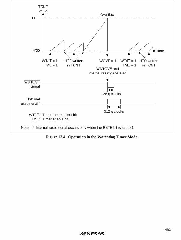
463
H'FF
H'00
Overflow
WT/IT = 1TME = 1
H'00 writtenin TCNT
Internalreset signal*
WDTOVFsignal
TCNTvalue
WDTOVF andinternal reset generated
WOVF = 1 WT/IT = 1TME = 1
WT/IT:TME:
Timer mode select bitTimer enable bit
H'00 writtenin TCNT
Time
512 φ clocks
128 φ clocks
Note: * Internal reset signal occurs only when the RSTE bit is set to 1.
Figure 13.4 Operation in the Watchdog Timer Mode

464
13.3.2 Interval Timer Mode
To use the WDT as an interval timer, clear WT/IT to 0 and set TME to 1. An interval timerinterrupt (ITI) is generated each time the timer counter overflows. This function can be used togenerate interval timer interrupts at regular intervals (figure 13.5).
H'FF
TCNT value
ITI: Interval timer interrupt request generation
H'00
WT/IT = 0TME = 1
ITI ITI ITI ITI
Time
Overflow Overflow Overflow Overflow
Figure 13.5 Operation in the Interval Timer Mode
13.3.3 Clearing the Standby Mode
The watchdog timer has a special function to clear the standby mode with an NMI interrupt. Whenusing the standby mode, set the WDT as described below.
Before Transition to the Standby Mode: The TME bit in the TCSR must be cleared to 0 to stopthe watchdog timer counter before it enters the standby mode. The chip cannot enter the standbymode while the TME bit is set to 1. Set bits CKS2–CKS0 so that the counter overflow interval isequal to or longer than the oscillation settling time. See sections 25.3, and 26.3, ACCharacteristics, for the oscillation settling time.
Recovery from the Standby Mode: When an NMI request signal is received in standby mode,the clock oscillator starts running and the watchdog timer starts incrementing at the rate selectedby bits CKS2–CKS0 before the standby mode was entered. When the TCNT overflows (changesfrom H'FF to H'00), the clock is presumed to be stable and usable; clock signals are supplied to theentire chip and the standby mode ends.
For details on the standby mode, see section 24, Power-Down State.

465
13.3.4 Timing of Setting the Overflow Flag (OVF)
In the interval timer mode, when the TCNT overflows, the OVF flag of the TCSR is set to 1 andan interval timer interrupt is simultaneously requested (figure 13.6).
H'FF H'00
CK
TCNT
Overflow signal(internal signal)
OVF
Figure 13.6 Timing of Setting the OVF
13.3.5 Timing of Setting the Watchdog Timer Overflow Flag (WOVF)
When the TCNT overflows in the watchdog timer mode, the WOVF bit of the RSTCSR is set to 1and a WDTOVF signal is output. When the RSTE bit is set to 1, TCNT overflow enables aninternal reset signal to be generated for the entire chip (figure 13.7).
H'FF H'00
CK
TCNT
Overflow signal(internal signal)
WOVF
Figure 13.7 Timing of Setting the WOVF Bit

466
13.4 Notes on Use
13.4.1 TCNT Write and Increment Contention
If a timer counter (TCNT) increment clock pulse is generated during the T3 state of a write cycleto the TCNT, the write takes priority and the timer counter is not incremented (figure 13.8).
CK
Address
Internalwrite signal
TCNTinput clock
TCNT N M
TCNT address
Counter write data
T1 T2 T3
TCNT write cycle
Figure 13.8 Contention between TCNT Write and Increment
13.4.2 Changing CKS2–CKS0 Bit Values
If the values of bits CKS2–CKS0 are altered while the WDT is running, the count may incrementincorrectly. Always stop the watchdog timer (by clearing the TME bit to 0) before changing thevalues of bits CKS2–CKS0.
13.4.3 Changing between Watchdog Timer/Interval Timer Modes
To prevent incorrect operation, always stop the watchdog timer (by clearing the TME bit to 0)before switching between interval timer mode and watchdog timer mode.
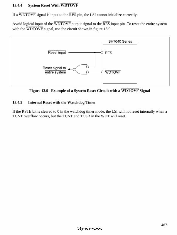
467
13.4.4 System Reset With WDTOVF
If a WDTOVF signal is input to the RES pin, the LSI cannot initialize correctly.
Avoid logical input of the WDTOVF output signal to the RES input pin. To reset the entire systemwith the WDTOVF signal, use the circuit shown in figure 13.9.
Reset input
Reset signal toentire system
SH7040 Series
RES
WDTOVF
Figure 13.9 Example of a System Reset Circuit with a WDTOVF Signal
13.4.5 Internal Reset with the Watchdog Timer
If the RSTE bit is cleared to 0 in the watchdog timer mode, the LSI will not reset internally when aTCNT overflow occurs, but the TCNT and TCSR in the WDT will reset.

468

469
Section 14 Serial Communication Interface (SCI)
14.1 Overview
The SH7040 Series has a serial communication interface (SCI) with two independent channels,both of which possess the same functions.
The SCI supports both asynchronous and clock synchronous serial communication. It also has amultiprocessor communication function for serial communication among two or more processors.
14.1.1 Features
• Select asynchronous or clock synchronous as the serial communications mode.
Asynchronous mode: Serial data communications are synched by start-stop in characterunits. The SCI can communicate with a universal asynchronous receiver/transmitter(UART), an asynchronous communication interface adapter (ACIA), or any other chip thatemploys a standard asynchronous serial communication. It can also communicate with twoor more other processors using the multiprocessor communication function. There aretwelve selectable serial data communication formats.
Data length: seven or eight bits
Stop bit length: one or two bits
Parity: even, odd, or none
Multiprocessor bit: one or none
Receive error detection: parity, overrun, and framing errors
Break detection: by reading the RxD level directly when a framing error occurs
Clocked synchronous mode: Serial data communication is synchronized with a clocksignal. The SCI can communicate with other chips having a clock synchronouscommunication function. There is one serial data communication format.
Data length: eight bits
Receive error detection: overrun errors
• Full duplex communication: The transmitting and receiving sections are independent, so theSCI can transmit and receive simultaneously. Both sections use double buffering, socontinuous data transfer is possible in both the transmit and receive directions.
• On-chip baud rate generator with selectable bit rates.
• Internal or external transmit/receive clock source: baud rate generator (internal) or SCK pin(external).
• Four types of interrupts: Transmit-data-empty, transmit-end, receive-data-full, and receive-error interrupts are requested independently. The transmit-data-empty and receive-data-fullinterrupts can start the direct memory access controller (DMAC)/data transfer controller (DTC)to transfer data.

470
14.1.2 Block Diagram
Figure 14.1 shows a block diagram of the SCI.
Paritygeneration
Parity check
Transmit/receive control
Baud rate generator
Clock
External clock
Bus
inte
rfac
e
Internaldata bus
RxD
RDR TDR
RSR TSR
SSR
SCR
SMR
BRR
φφ/4φ/16φ/64
TEITxIRxIERI
SCK
::::
RSRRDRTSRTDR
Receive shift registerReceive data registerTransmit shift registerTransmit data register
::::
SMRSCRSSRBRR
Serial mode registerSerial control registerSerial status registerBit rate register
TxD
SCI
Module data bus
Figure 14.1 SCI Block Diagram

471
14.1.3 Pin Configuration
Table 14.1 summarizes the SCI pins by channel.
Table 14.1 SCI Pins
Channel Pin Name Abbreviation Input/Output Function
0 Serial clock pin SCK0 Input/output SCI0 clock input/output
Receive data pin RxD0 Input SCI0 receive data input
Transmit data pin TxD0 Output SCI0 transmit data output
1 Serial clock pin SCK1 Input/output SCI1 clock input/output
Receive data pin RxD1 Input SCI1 receive data input
Transmit data pin TxD1 Output SCI1 transmit data output
14.1.4 Register Configuration
Table 14.2 summarizes the SCI internal registers. These registers select the communication mode(asynchronous or clock synchronous), specify the data format and bit rate, and control thetransmitter and receiver sections.
Table 14.2 Registers
Channel Name Abbreviation R/WInitialValue Address * 2
AccessSize
0 Serial mode register SMR0 R/W H'00 H'FFFF81A0 8, 16
Bit rate register BRR0 R/W H'FF H'FFFF81A1 8, 16
Serial control register SCR0 R/W H'00 H'FFFF81A2 8, 16
Transmit data register TDR0 R/W H'FF H'FFFF81A3 8, 16
Serial status register SSR0 R/(W)* 1 H'84 H'FFFF81A4 8, 16
Receive data register RDR0 R H'00 H'FFFF81A5 8, 16
1 Serial mode register SMR1 R/W H'00 H'FFFF81B0 8, 16
Bit rate register BRR1 R/W H'FF H'FFFF81B1 8, 16
Serial control register SCR1 R/W H'00 H'FFFF81B2 8, 16
Transmit data register TDR1 R/W H'FF H'FFFF81B3 8, 16
Serial status register SSR1 R/(W)* 1 H'84 H'FFFF81B4 8, 16
Receive data register RDR1 R H'00 H'FFFF81B5 8, 16
Notes: * 1 The only value that can be written is a 0 to clear the flags.* 2 Do not access empty addresses.

472
14.2 Register Descriptions
14.2.1 Receive Shift Register (RSR)
The receive shift register (RSR) receives serial data. Data input at the RxD pin is loaded into theRSR in the order received, LSB (bit 0) first, converting the data to parallel form. When one bytehas been received, it is automatically transferred to the RDR.
The CPU cannot read or write the RSR directly.
Bit: 7 6 5 4 3 2 1 0
R/W: — — — — — — — —
14.2.2 Receive Data Register (RDR)
The receive data register (RDR) stores serial receive data. The SCI completes the reception of onebyte of serial data by moving the received data from the receive shift register (RSR) into the RDRfor storage. The RSR is then ready to receive the next data. This double buffering allows the SCIto receive data continuously.
The CPU can read but not write the RDR. The RDR is initialized to H'00 by a power-on reset or instandby mode. Manual reset does not initialize RDR.
Bit: 7 6 5 4 3 2 1 0
Initial value: 0 0 0 0 0 0 0 0
R/W: R R R R R R R R
14.2.3 Transmit Shift Register (TSR)
The transmit shift register (TSR) transmits serial data. The SCI loads transmit data from thetransmit data register (TDR) into the TSR, then transmits the data serially from the TxD pin, LSB(bit 0) first. After transmitting one data byte, the SCI automatically loads the next transmit datafrom the TDR into the TSR and starts transmitting again. If the TDRE bit of the SSR is 1,however, the SCI does not load the TDR contents into the TSR.

473
The CPU cannot read or write the TSR directly.
Bit: 7 6 5 4 3 2 1 0
R/W: — — — — — — — —
14.2.4 Transmit Data Register (TDR)
The transmit data register (TDR) is an 8-bit register that stores data for serial transmission. Whenthe SCI detects that the transmit shift register (TSR) is empty, it moves transmit data written in theTDR into the TSR and starts serial transmission. Continuous serial transmission is possible bywriting the next transmit data in the TDR during serial transmission from the TSR.
The CPU can always read and write the TDR. The TDR is initialized to H'FF by a power-on resetor in standby mode. Manual reset does not initialize TDR.
Bit: 7 6 5 4 3 2 1 0
Initial value: 1 1 1 1 1 1 1 1
R/W: R/W R/W R/W R/W R/W R/W R/W R/W
14.2.5 Serial Mode Register (SMR)
The serial mode register (SMR) is an 8-bit register that specifies the SCI serial communicationformat and selects the clock source for the baud rate generator.
The CPU can always read and write the SMR. The SMR is initialized to H'00 by a power-on resetor in standby mode. Manual reset does not initialize SMR.
Bit: 7 6 5 4 3 2 1 0
C/A CHR PE O/E STOP MP CKS1 CKS0
Initial value: 0 0 0 0 0 0 0 0
R/W: R/W R/W R/W R/W R/W R/W R/W R/W

474
• Bit 7—Communication Mode (C/A): Selects whether the SCI operates in the asynchronous orclock synchronous mode.
Bit 7: C/ A Description
0 Asynchronous mode (initial value)
1 Clocked synchronous mode
• Bit 6—Character Length (CHR): Selects 7-bit or 8-bit data in the asynchronous mode. In theclock synchronous mode, the data length is always eight bits, regardless of the CHR setting.
Bit 6: CHR Description
0 Eight-bit data (initial value)
1 Seven-bit data. (When 7-bit data is selected, the MSB (bit 7) of thetransmit data register is not transmitted.)
• Bit 5—Parity Enable (PE): Selects whether to add a parity bit to transmit data and to check theparity of receive data, in the asynchronous mode. In the clock synchronous mode, a parity bit isneither added nor checked, regardless of the PE setting.
Bit 5: PE Description
0 Parity bit not added or checked (initial value)
1 Parity bit added and checked. When PE is set to 1, an even or oddparity bit is added to transmit data, depending on the parity mode (O/E)setting. Receive data parity is checked according to the even/odd (O/E)mode setting.
• Bit 4—Parity Mode (O/E): Selects even or odd parity when parity bits are added and checked.The O/E setting is used only in asynchronous mode and only when the parity enable bit (PE) isset to 1 to enable parity addition and check. The O/E setting is ignored in the clocksynchronous mode, or in the asynchronous mode when parity addition and check is disabled.
Bit 4: O/ E Description
0 Even parity (initial value). If even parity is selected, the parity bit isadded to transmit data to make an even number of 1s in the transmittedcharacter and parity bit combined. Receive data is checked to see if ithas an even number of 1s in the received character and parity bitcombined.
1 Odd parity. If odd parity is selected, the parity bit is added to transmitdata to make an odd number of 1s in the transmitted character andparity bit combined. Receive data is checked to see if it has an oddnumber of 1s in the received character and parity bit combined.

475
• Bit 3—Stop Bit Length (STOP): Selects one or two bits as the stop bit length in theasynchronous mode. This setting is used only in the asynchronous mode. It is ignored in theclock synchronous mode because no stop bits are added.
In receiving, only the first stop bit is checked, regardless of the STOP bit setting. If the secondstop bit is 1, it is treated as a stop bit, but if the second stop bit is 0, it is treated as the start bitof the next incoming character.
Bit 3: STOP Description
0 One stop bit (initial value). In transmitting, a single bit of 1 is added atthe end of each transmitted character.
1 Two stop bits. In transmitting, two bits of 1 are added at the end of eachtransmitted character.
• Bit 2—Multiprocessor Mode (MP): Selects multiprocessor format. When multiprocessorformat is selected, settings of the parity enable (PE) and parity mode (O/E) bits are ignored.The MP bit setting is used only in the asynchronous mode; it is ignored in the clocksynchronous mode. For the multiprocessor communication function, see section 14.3.3,Multiprocessor Communication.
Bit 2: MP Description
0 Multiprocessor function disabled (initial value)
1 Multiprocessor format selected
• Bits 1 and 0—Clock Select 1 and 0 (CKS1 and CKS0): These bits select the internal clocksource of the on-chip baud rate generator. Four clock sources are available; φ, φ/4, φ/16, orφ/64. For further information on the clock source, bit rate register settings, and baud rate, seesection 14.2.8, Bit Rate Register (BRR).
Bit 1: CKS1 Bit 0: CKS0 Description
0 0 φ (initial value)
1 φ/4
1 0 φ/16
1 φ/64

476
14.2.6 Serial Control Register (SCR)
The serial control register (SCR) operates the SCI transmitter/receiver, selects the serial clockoutput in the asynchronous mode, enables/disables interrupt requests, and selects thetransmit/receive clock source. The CPU can always read and write the SCR. The SCR is initializedto H'00 by a power-on reset or in standby mode. Manual reset does not initialize SCR.
Bit: 7 6 5 4 3 2 1 0
TIE RIE TE RE MPIE TEIE CKE1 CKE0
Initial value: 0 0 0 0 0 0 0 0
R/W: R/W R/W R/W R/W R/W R/W R/W R/W
• Bit 7—Transmit Interrupt Enable (TIE): Enables or disables the transmit-data-empty interrupt(TxI) requested when the transmit data register empty bit (TDRE) in the serial status register(SSR) is set to 1 by transfer of serial transmit data from the TDR to the TSR.
Bit 7: TIE Description
0 Transmit-data-empty interrupt request (TxI) is disabled (initial value).The TxI interrupt request can be cleared by reading TDRE after it hasbeen set to 1, then clearing TDRE to 0, or by clearing TIE to 0.
1 Transmit-data-empty interrupt request (TxI) is enabled
• Bit 6—Receive Interrupt Enable (RIE): Enables or disables the receive-data-full interrupt (RxI)requested when the receive data register full bit (RDRF) in the serial status register (SSR) is setto 1 by transfer of serial receive data from the RSR to the RDR. It also enables or disablesreceive-error interrupt (ERI) requests.
Bit 6: RIE Description
0 Receive-data-full interrupt (RxI) and receive-error interrupt (ERI)requests are disabled (initial value). RxI and ERI interrupt requests canbe cleared by reading the RDRF flag or error flag (FER, PER, or ORER)after it has been set to 1, then clearing the flag to 0, or by clearing RIEto 0.
1 Receive-data-full interrupt (RxI) and receive-error interrupt (ERI)requests are enabled.

477
• Bit 5—Transmit Enable (TE): Enables or disables the SCI serial transmitter.
Bit 5: TE Description
0 Transmitter disabled (initial value). The transmit data register empty bit(TDRE) in the serial status register (SSR) is locked at 1.
1 Transmitter enabled. Serial transmission starts when the transmit dataregister empty (TDRE) bit in the serial status register (SSR) is cleared to0 after writing of transmit data into the TDR. Select the transmit formatin the SMR before setting TE to 1.
• Bit 4—Receive Enable (RE): Enables or disables the SCI serial receiver.
Bit 4: RE Description
0 Receiver disabled (initial value). Clearing RE to 0 does not affect thereceive flags (RDRF, FER, PER, ORER). These flags retain theirprevious values.
1 Receiver enabled. Serial reception starts when a start bit is detected inthe asynchronous mode, or synchronous clock input is detected in theclock synchronous mode. Select the receive format in the SMR beforesetting RE to 1.
• Bit 3—Multiprocessor Interrupt Enable (MPIE): Enables or disables multiprocessor interrupts.The MPIE setting is used only in the asynchronous mode, and only if the multiprocessor modebit (MP) in the serial mode register (SMR) is set to 1 during reception. The MPIE setting isignored in the clock synchronous mode or when the MP bit is cleared to 0.
Bit 3: MPIE Description
0 Multiprocessor interrupts are disabled (normal receive operation) (initialvalue). MPIE is cleared when the MPIE bit is cleared to 0, or themultiprocessor bit (MPB) is set to 1 in receive data.
1 Multiprocessor interrupts are enabled. Receive-data-full interruptrequests (RxI), receive-error interrupt requests (ERI), and setting of theRDRF, FER, and ORER status flags in the serial status register (SSR)are disabled until data with the multiprocessor bit set to 1 is received.
The SCI does not transfer receive data from the RSR to the RDR, doesnot detect receive errors, and does not set the RDRF, FER, and ORERflags in the serial status register (SSR). When it receives data thatincludes MPB = 1, MPB is set to 1, and the SCI automatically clearsMPIE to 0, generates RxI and ERI interrupts (if the TIE and RIE bits inthe SCR are set to 1), and allows the FER and ORER bits to be set.

478
• Bit 2—Transmit-End Interrupt Enable (TEIE): Enables or disables the transmit-end interrupt(TEI) requested if TDR does not contain valid transmit data when the MSB is transmitted.
Bit 2: TEIE Description
0 Transmit-end interrupt (TEI) requests are disabled.* (initial value)
1 Transmit-end interrupt (TEI) requests are enabled.*
Note: * The TEI request can be cleared by reading the TDRE bit in the serial status register (SSR)after it has been set to 1, then clearing TDRE to 0 and clearing the transmit end (TEND)bit to 0; or by clearing the TEIE bit to 0.
• Bits 1 and 0—Clock Enable 1 and 0 (CKE1 and CKE0): These bits select the SCI clock sourceand enable or disable clock output from the SCK pin. Depending on the combination of CKE1and CKE0, the SCK pin can be used for serial clock output, or serial clock input. Select theSCK pin function by using the pin function controller (PFC).
The CKE0 setting is valid only in the asynchronous mode, and only when the SCI is internallyclocked (CKE1 = 0). The CKE0 setting is ignored in the clock synchronous mode, or when anexternal clock source is selected (CKE1 = 1). Select the SCI operating mode in the serial moderegister (SMR) before setting CKE1 and CKE0. For further details on selection of the SCIclock source, see table 14.9 in section 14.3, Operation.
Bit 1:CKE1
Bit 0:CKE0 Description * 1
0 0 Asynchronous mode Internal clock, SCK pin used for input pin (input signalis ignored) or output pin (output level is undefined)* 2
Clock synchronous mode Internal clock, SCK pin used for synchronous clockoutput* 2
0 1 Asynchronous mode Internal clock, SCK pin used for clock output* 3
Clock synchronous mode Internal clock, SCK pin used for synchronous clockoutput
1 0 Asynchronous mode External clock, SCK pin used for clock input* 4
Clock synchronous mode External clock, SCK pin used for synchronous clockinput
1 1 Asynchronous mode External clock, SCK pin used for clock input* 4
Clock synchronous mode External clock, SCK pin used for synchronous clockinput
Notes: * 1 The SCK pin is multiplexed with other functions. Use the pin function controller (PFC) toselect the SCK function for this pin, as well as the I/O direction.
* 2 Initial value.* 3 The output clock frequency is the same as the bit rate.* 4 The input clock frequency is 16 times the bit rate.

479
14.2.7 Serial Status Register (SSR)
The serial status register (SSR) is an 8-bit register containing multiprocessor bit values, and statusflags that indicate SCI operating status.
The CPU can always read and write the SSR, but cannot write 1 in the status flags (TDRE, RDRF,ORER, PER, and FER). These flags can be cleared to 0 only if they have first been read (afterbeing set to 1). Bits 2 (TEND) and 1 (MPB) are read-only bits that cannot be written. The SSR isinitialized to H'84 by a power-on reset or in standby mode. Manual reset does not initialize SSR.
Bit: 7 6 5 4 3 2 1 0
TDRE RDRF ORER FER PER TEND MPB MPBT
Initial value: 1 0 0 0 0 1 0 0
R/W: R/(W)* R/(W)* R/(W)* R/(W)* R/(W)* R R R/W
Note: * The only value that can be written is a 0 to clear the flag.
• Bit 7—Transmit Data Register Empty (TDRE): Indicates that the SCI has loaded transmit datafrom the TDR into the TSR and new serial transmit data can be written in the TDR.
Bit 7: TDRE Description
0 TDR contains valid transmit data
TDRE is cleared to 0 when software reads TDRE after it has been set to 1, thenwrites 0 in TDRE or the DMAC or DTC writes data in TDR
1 TDR does not contain valid transmit data (initial value)
TDRE is set to 1 when the chip is power-on reset or enters standby mode, the TEbit in the serial control register (SCR) is cleared to 0, or TDR contents are loadedinto TSR, so new data can be written in TDR

480
• Bit 6—Receive Data Register Full (RDRF): Indicates that RDR contains received data.
Bit 6: RDRF Description
0 RDR does not contain valid received data (initial value)
RDRF is cleared to 0 when the chip is power-on reset or enters standby mode,software reads RDRF after it has been set to 1, then writes 0 in RDRF, or theDMAC or DTC reads data from RDR
1 RDR contains valid received data
RDRF is set to 1 when serial data is received normally and transferred from RSRto RDR
Note: The RDR and RDRF are not affected by detection of receive errors or by clearing of the REbit to 0 in the serial control register. They retain their previous contents. If RDRF is still setto 1 when reception of the next data ends, an overrun error (ORER) occurs and thereceived data is lost.
• Bit 5—Overrun Error (ORER): Indicates that data reception ended abnormally due to anoverrun error.
Bit 5: ORER Description
0 Receiving is in progress or has ended normally (initial value). Clearing the RE bitto 0 in the serial control register does not affect the ORER bit, which retains itsprevious value.
ORER is cleared to 0 when the chip is power-on reset or enters standby mode orsoftware reads ORER after it has been set to 1, then writes 0 in ORER
1 A receive overrun error occurred. RDR continues to hold the data receivedbefore the overrun error, so subsequent receive data is lost. Serial receivingcannot continue while ORER is set to 1. In the clock synchronous mode, serialtransmitting is disabled.
ORER is set to 1 if reception of the next serial data ends when RDRF is set to 1

481
• Bit 4—Framing Error (FER): Indicates that data reception ended abnormally due to a framingerror in the asynchronous mode.
Bit 4: FER Description
0 Receiving is in progress or has ended normally (initial value). Clearing the RE bitto 0 in the serial control register does not affect the FER bit, which retains itsprevious value.
FER is cleared to 0 when the chip is power-on reset or enters standby mode orsoftware reads FER after it has been set to 1, then writes 0 in FER
1 A receive framing error occurred. When the stop bit length is two bits, only thefirst bit is checked to see if it is a 1. The second stop bit is not checked. When aframing error occurs, the SCI transfers the receive data into the RDR but doesnot set RDRF. Serial receiving cannot continue while FER is set to 1. In the clocksynchronous mode, serial transmitting is also disabled.
FER is set to 1 if the stop bit at the end of receive data is checked and found tobe 0
• Bit 3—Parity Error (PER): Indicates that data reception (with parity) ended abnormally due toa parity error in the asynchronous mode.
Bit 3: PER Description
0 Receiving is in progress or has ended normally (initial value). Clearing the RE bitto 0 in the serial control register does not affect the PER bit, which retains itsprevious value.
PER is cleared to 0 when the chip is power-on reset or enters standby mode orsoftware reads PER after it has been set to 1, then writes 0 in PER
1 A receive parity error occurred. When a parity error occurs, the SCI transfers thereceive data into the RDR but does not set RDRF. Serial receiving cannotcontinue while PER is set to 1. In the clock synchronous mode, serial transmittingis also disabled.
PER is set to 1 if the number of 1s in receive data, including the parity bit, doesnot match the even or odd parity setting of the parity mode bit (O/E) in the serialmode register (SMR)

482
• Bit 2—Transmit End (TEND): Indicates that when the last bit of a serial character wastransmitted, the TDR did not contain valid data, so transmission has ended. TEND is a read-only bit and cannot be written.
Bit 2: TEND Description
0 Transmission is in progress
TEND is cleared to 0 when software reads TDRE after it has been set to 1, thenwrites 0 in TDRE, or the DMAC or DTC writes data in TDR
1 End of transmission (initial value)
TEND is set to 1 when the chip is power-on reset or enters standby mode, TE iscleared to 0 in the serial control register (SCR), or TDRE is 1 when the last bit ofa one-byte serial character is transmitted.
• Bit 1—Multiprocessor Bit (MPB): Stores the value of the multiprocessor bit in receive datawhen a multiprocessor format is selected for receiving in the asynchronous mode. The MPB isa read-only bit and cannot be written.
Bit 1: MPB Description
0 Multiprocessor bit value in receive data is 0 (initial value). If RE is cleared to 0when a multiprocessor format is selected, the MPB retains its previous value.
1 Multiprocessor bit value in receive data is 1
• Bit 0—Multiprocessor Bit Transfer (MPBT): Stores the value of the multiprocessor bit addedto transmit data when a multiprocessor format is selected for transmitting in the asynchronousmode. The MPBT setting is ignored in the clock synchronous mode, when a multiprocessorformat is not selected, or when the SCI is not transmitting.
Bit 0: MPBT Description
0 Multiprocessor bit value in transmit data is 0 (initial value)
1 Multiprocessor bit value in transmit data is 1

483
14.2.8 Bit Rate Register (BRR)
The bit rate register (BRR) is an 8-bit register that, together with the baud rate generator clocksource selected by the CKS1 and CKS0 bits in the serial mode register (SMR), determines theserial transmit/receive bit rate.
The CPU can always read and write the BRR. The BRR is initialized to H'FF by a power-on resetor in standby mode. Each channel has independent baud rate generator control, so different valuescan be set in the two channels. Manual reset does not initialize BRR.
Bit: 7 6 5 4 3 2 1 0
Initial value: 1 1 1 1 1 1 1 1
R/W: R/W R/W R/W R/W R/W R/W R/W R/W
Table 14.3 lists examples of BRR settings in the asynchronous mode; table 14.4 lists examples ofBBR settings in the clock synchronous mode.
Table 14.3 Bit Rates and BRR Settings in Asynchronous Mode
φ (MHz)
Bit Rate 4 4.9152 6
(Bits/s) n N Error (%) n N Error (%) n N Error (%)
110 2 70 0.03 2 86 0.31 2 106 –0.44
150 1 207 0.16 1 255 0.00 2 77 0.16
300 1 103 0.16 1 127 0.00 1 155 0.16
600 0 207 0.16 0 255 0.00 1 77 0.16
1200 0 103 0.16 0 127 0.00 0 155 0.16
2400 0 51 0.16 0 63 0.00 0 77 0.16
4800 0 25 0.16 0 31 0.00 0 38 0.16
9600 0 12 0.16 0 15 0.00 0 19 –2.34
14400 0 8 –3.55 0 10 –3.03 0 12 0.16
19200 0 6 –6.99 0 7 0.00 0 9 –2.34
28800 0 3 8.51 0 4 6.67 0 6 –6.99
31250 0 3 0.00 0 4 –1.70 0 5 0.00
38400 0 2 8.51 0 3 0.00 0 4 –2.34

484
Table 14.3 Bit Rates and BRR Settings in Asynchronous Mode (cont)
φ (MHz)
Bit Rate 7.3728 8 9.8304
(Bits/s) n N Error (%) n N Error (%) n N Error (%)
110 2 130 –0.07 2 141 0.03 2 174 –0.26
150 2 95 0.00 2 103 0.16 2 127 0.00
300 1 191 0.00 1 207 0.16 1 255 0.00
600 1 95 0.00 1 103 0.16 1 127 0.00
1200 0 191 0.00 0 207 0.16 0 255 0.00
2400 0 95 0.00 0 103 0.16 0 127 0.00
4800 0 47 0.00 0 51 0.16 0 63 0.00
9600 0 23 0.00 0 25 0.16 0 31 0.00
14400 0 15 0.00 0 16 2.12 0 20 1.59
19200 0 11 0.00 0 12 0.16 0 15 0.00
28800 0 7 0.00 0 8 –3.55 0 10 –3.03
31250 0 6 5.33 0 7 0.00 0 9 –1.70
38400 0 5 0.00 0 6 –6.99 0 7 0.00

485
Table 14.3 Bit Rates and BRR Settings in Asynchronous Mode (cont)
φ (MHz)
Bit Rate 10 11.0592 12
(Bits/s) n N Error (%) n N Error (%) n N Error (%)
110 2 177 –0.25 2 195 0.19 2 212 0.03
150 2 129 0.16 2 143 0.00 2 155 0.16
300 2 64 0.16 2 71 0.00 2 77 0.16
600 1 129 0.16 1 143 0.00 1 155 0.16
1200 1 64 0.16 1 71 0.00 1 77 0.16
2400 0 129 0.16 0 143 0.00 0 155 0.16
4800 0 64 0.16 0 71 0.00 0 77 0.16
9600 0 32 –1.36 0 35 0.00 0 38 0.16
14400 0 21 –1.36 0 23 0.00 0 25 0.16
19200 0 15 1.73 0 17 0.00 0 19 –2.34
28800 0 10 –1.36 0 11 0.00 0 12 0.16
31250 0 9 0.00 0 10 0.54 0 11 0.00
38400 0 7 1.73 0 8 0.00 0 9 –2.34

486
Table 14.3 Bit Rates and BRR Settings in Asynchronous Mode (cont)
φ (MHz)
Bit Rate 12.288 14 14.7456
(Bits/s) n N Error (%) n N Error (%) n N Error (%)
110 2 217 0.08 2 248 –0.17 3 64 0.70
150 2 159 0.00 2 181 0.16 2 191 0.00
300 2 79 0.00 2 90 0.16 2 95 0.00
600 1 159 0.00 1 181 0.16 1 191 0.00
1200 1 79 0.00 1 90 0.16 1 95 0.00
2400 0 159 0.00 0 181 0.16 0 191 0.00
4800 0 79 0.00 0 90 0.16 0 95 0.00
9600 0 39 0.00 0 45 –0.93 0 47 0.00
14400 0 26 –1.23 0 29 1.27 0 31 0.00
19200 0 19 0.00 0 22 –0.93 0 23 0.00
28800 0 12 2.56 0 14 1.27 0 15 0.00
31250 0 11 2.40 0 13 0.00 0 14 –1.70
38400 0 9 0.00 0 10 3.57 0 11 0.00

487
Table 14.3 Bit Rates and BRR Settings in Asynchronous Mode (cont)
φ (MHz)
Bit Rate 16 17.2032 18
(Bits/s) n N Error (%) n N Error (%) n N Error (%)
110 3 70 0.03 3 75 0.48 3 79 –0.12
150 2 207 0.16 2 223 0.00 2 233 0.16
300 2 103 0.16 2 111 0.00 2 116 0.16
600 1 207 0.16 1 223 0.00 1 233 0.16
1200 1 103 0.16 1 111 0.00 1 116 0.16
2400 0 207 0.16 0 223 0.00 0 233 0.16
4800 0 103 0.16 0 111 0.00 0 116 0.16
9600 0 51 0.16 0 55 0.00 0 58 –0.69
14400 0 34 –0.79 0 36 0.90 0 38 0.16
19200 0 25 0.16 0 27 0.00 0 28 1.02
28800 0 16 2.12 0 18 –1.75 0 19 –2.34
31250 0 15 0.00 0 16 1.20 0 17 0.00
38400 0 12 0.16 0 13 0.00 0 14 –2.34
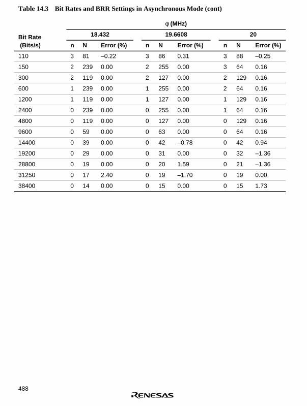
488
Table 14.3 Bit Rates and BRR Settings in Asynchronous Mode (cont)
φ (MHz)
Bit Rate 18.432 19.6608 20
(Bits/s) n N Error (%) n N Error (%) n N Error (%)
110 3 81 –0.22 3 86 0.31 3 88 –0.25
150 2 239 0.00 2 255 0.00 3 64 0.16
300 2 119 0.00 2 127 0.00 2 129 0.16
600 1 239 0.00 1 255 0.00 2 64 0.16
1200 1 119 0.00 1 127 0.00 1 129 0.16
2400 0 239 0.00 0 255 0.00 1 64 0.16
4800 0 119 0.00 0 127 0.00 0 129 0.16
9600 0 59 0.00 0 63 0.00 0 64 0.16
14400 0 39 0.00 0 42 –0.78 0 42 0.94
19200 0 29 0.00 0 31 0.00 0 32 –1.36
28800 0 19 0.00 0 20 1.59 0 21 –1.36
31250 0 17 2.40 0 19 –1.70 0 19 0.00
38400 0 14 0.00 0 15 0.00 0 15 1.73

489
Table 14.3 Bit Rates and BRR Settings in Asynchronous Mode (cont)
φ (MHz)
Bit Rate 22 22.1184 24
(Bits/s) n N Error (%) n N Error (%) n N Error (%)
110 3 97 –0.35 3 97 0.19 3 106 –0.44
150 3 71 –0.54 3 71 0.00 3 77 0.16
300 2 142 0.16 2 143 0.00 2 155 0.16
600 2 71 –0.54 2 71 0.00 2 77 0.16
1200 1 142 0.16 1 143 0.00 1 155 0.16
2400 1 71 –0.54 1 71 0.00 1 77 0.16
4800 0 142 0.16 0 143 0.00 0 155 0.16
9600 0 71 –0.54 0 71 0.00 0 77 0.16
14400 0 47 –0.54 0 47 0.00 0 51 0.16
19200 0 35 –0.54 0 35 0.00 0 38 0.16
28800 0 23 –0.54 0 23 0.00 0 25 0.16
31250 0 21 0.00 0 21 0.54 0 23 0.00
38400 0 17 –0.54 0 17 0.00 0 19 –2.34

490
Table 14.3 Bit Rates and BRR Settings in Asynchronous Mode (cont)
φ (MHz)
Bit Rate 24.576 25.8048 26
(Bits/s) n N Error (%) n N Error (%) n N Error (%)
110 3 108 0.08 3 114 –0.40 3 114 0.36
150 3 79 0.00 3 83 0.00 3 84 –0.43
300 2 159 0.00 2 167 0.00 2 168 0.16
600 2 79 0.00 2 83 0.00 2 84 –0.43
1200 1 159 0.00 1 167 0.00 1 168 0.16
2400 1 79 0.00 1 83 0.00 1 84 –0.43
4800 0 159 0.00 0 167 0.00 0 168 0.16
9600 0 79 0.00 0 83 0.00 0 84 –0.43
14400 0 52 0.63 0 55 0.00 0 55 0.76
19200 0 39 0.00 0 41 0.00 0 41 0.76
28800 0 26 –1.23 0 27 0.00 0 27 0.76
31250 0 24 –1.70 0 25 –0.75 0 25 0.00
38400 0 19 0.00 0 20 0.00 0 20 0.76

491
Table 14.3 Bit Rates and BRR Settings in Asynchronous Mode (cont)
φ (MHz)
Bit Rate 27.0336 28 29.4912
(Bits/s) n N Error (%) n N Error (%) n N Error (%)
110 3 119 0.00 3 123 0.23 3 130 -0.07
150 3 87 0.00 3 90 0.16 3 95 0.00
300 2 175 0.00 2 181 0.16 2 191 0.00
600 1 87 0.00 2 90 0.16 2 95 0.00
1200 1 175 0.00 1 181 0.16 1 191 0.00
2400 1 87 0.00 1 90 0.16 1 95 0.00
4800 0 175 0.00 0 181 0.16 0 191 0.00
9600 0 87 0.00 0 90 0.16 0 95 0.00
14400 0 58 –0.56 0 60 –0.39 0 63 0.00
19200 0 43 0.00 0 45 0.93 0 47 0.00
28800 0 28 1.15 0 29 1.27 0 31 0.00
31250 0 26 0.12 0 27 0.00 0 28 1.69
38400 0 21 0.00 0 22 –0.93 0 23 0.00

492
Table 14.3 Bit Rates and BRR Settings in Asynchronous Mode (cont)
φ (MHz)
Bit Rate 30 31.9488 32
(Bits/s) n N Error (%) n N Error (%) n N Error (%)
110 3 132 0.13 3 141 -0.13 3 141 0.03
150 3 97 -0.35 3 103 0.00 3 103 0.16
300 2 194 0.16 2 207 0.00 2 207 0.16
600 2 97 -0.35 2 103 0.00 2 103 0.16
1200 1 194 0.16 1 207 0.00 1 207 0.16
2400 1 97 -0.35 1 103 0.00 1 103 0.16
4800 0 194 0.16 0 207 0.00 0 207 0.16
9600 0 97 -0.35 0 103 0.00 0 103 0.16
14400 0 64 0.16 0 68 0.48 0 68 0.64
19200 0 48 -0.35 0 51 0.00 0 51 0.16
28800 0 32 -1.36 0 34 -0.95 0 34 -0.79
31250 0 29 0.00 0 31 -0.16 0 31 0.00
38400 0 23 1.73 0 25 0.00 0 25 0.16

493
Table 14.3 Bit Rates and BRR Settings in Asynchronous Mode (cont)
φ (MHz)
Bit Rate 33 33.1776 33.3333
(Bits/s) n N Error (%) n N Error (%) n N Error (%)
110 3 145 0.33 3 146 0.19 3 147 -0.02
150 3 106 0.39 3 107 0.00 3 108 -0.45
300 2 214 -0.07 2 215 0.00 2 216 0.01
600 2 106 0.39 2 107 0.00 2 108 -0.45
1200 1 214 -0.07 1 215 0.00 1 216 0.01
2400 1 106 0.39 1 107 0.00 1 108 -0.45
4800 0 214 -0.07 0 215 0.00 0 216 0.01
9600 0 106 0.39 0 107 0.00 0 108 -0.45
14400 0 71 –0.54 0 91 0.00 0 91 0.47
19200 0 53 –0.54 0 53 0.00 0 53 0.47
28800 0 35 –0.54 0 35 0.00 0 35 0.47
31250 0 32 0.00 0 32 0.54 0 32 1.01
38400 0 26 –0.54 0 26 0.00 0 26 0.47

494
Table 14.4 Bit Rates and BRR Settings in Clocked Synchronous Mode
φ (MHz)
Bit Rate 4 8 10 12
(Bits/s) n N n N n N n N
110 3 141
250 2 249 3 124 3 155 3 187
500 2 124 2 249 3 77 3 93
1k 1 249 2 124 2 155 2 187
2.5k 1 99 1 199 1 249 2 74
5k 0 199 1 99 1 124 1 149
10k 0 99 0 199 0 249 1 74
25k 0 39 0 79 0 99 0 119
50k 0 19 0 39 0 49 0 59
100k 0 9 0 19 0 24 0 29
250k 0 3 0 7 0 9 0 11
500k 0 1 0 3 0 4 0 5
1M 0 0* 0 1 — — 0 2
2.5M 0 0* 0 0*
5M

495
Table 14.4 Bit Rates and BRR Settings in Clocked Synchronous Mode (cont)
φ (MHz)
Bit Rate 16 20 24 28
(Bits/s) n N n N n N n N
110
250 3 249
500 3 124 3 155 3 187 3 218
1k 2 249 3 77 3 93 3 108
2.5k 2 99 2 124 2 149 2 174
5k 1 199 1 249 2 74 2 87
10k 1 99 1 124 1 149 1 174
25k 0 159 0 199 0 239 1 69
50k 0 79 0 99 0 119 0 139
100k 0 39 0 49 0 59 0 69
250k 0 15 0 19 0 23 0 27
500k 0 7 0 9 0 11 0 13
1M 0 3 0 4 0 5 0 6
2.5M — — 0 1 — — 0 2
3.5M — — — — 0 1
5M 0 0* — — — —
7M — — 0 0*

496
Table 14.4 Bit Rates and BRR Settings in Clocked Synchronous Mode (cont)
φ (MHz)
Bit Rate 30 32 33 33.3333
(Bits/s) n N n N n N n N
110
250
500 3 233 3 249
1k 3 116 3 124 3 128 3 129
2.5k 2 187 2 199 2 205 2 207
5k 2 93 2 99 2 102 2 103
10k 1 187 1 199 1 205 1 207
25k 1 74 1 79 1 82 1 82
50k 0 149 0 159 0 164 0 166
100k 0 74 0 79 0 82 0 82
250k 0 29 0 31 0 32 0 32
500k 0 14 0 15 0 16 0 16
1M 0 7 0 7 0 7 0 7
2.5M 0 2 0 2 0 2 — —
5M — — — — — — — —
7M — — — — — — — —
Note: Settings with an error of 1% or less are recommended.LegendBlank: No setting available
—: Setting possible, but error occurs* : Continuous transmission/reception is not possible.
The BRR setting is calculated as follows:
Asynchronous mode:
N=64 × 2 × B
× 10 –12n–16φ
Synchronous mode:
64 × 2 × B2n–1
φN= × 10 –1
6

497
B: Bit rate (bit/s)N: Baud rate generator BRR setting (0 ≤ N ≤ 255)φ: Operating frequency (MHz)n: Baud rate generator input clock (n = 0 to 3)(See the following table for the clock sources and value of n.)
SMR Settings
n Clock Source CKS1 CKS2
0 φ 0 0
1 φ/4 0 1
2 φ/16 1 0
3 φ/64 1 1
The bit rate error in asynchronous mode is calculated as follows:
Error (%)(N+1) × B × 64 × 2
2n–1= × 100–1 6φ × 10
Table 14.5 indicates the maximum bit rates in the asynchronous mode when the baud rategenerator is being used for various frequencies. Tables 14.6 and 14.7 show the maximum rates forexternal clock input.

498
Table 14.5 Maximum Bit Rates for Various Frequencies with Baud Rate Generator(Asynchronous Mode)
Settings
φ (MHz) Maximum Bit Rate (Bits/s) n N
4 125000 0 0
4.9152 153600 0 0
6 187500 0 0
7.3728 230400 0 0
8 250000 0 0
9.8304 307200 0 0
10 312500 0 0
11.0592 345600 0 0
12 375000 0 0
12.288 384000 0 0
14 437500 0 0
14.7456 460800 0 0
16 500000 0 0
17.2032 537600 0 0
18 562500 0 0
18.432 576000 0 0
19.6608 614400 0 0
20 625000 0 0
22 687500 0 0
22.1184 691200 0 0
24 750000 0 0
24.576 768000 0 0
25.8048 806400 0 0
26 812500 0 0
27.0336 844800 0 0
28 875000 0 0
29.4912 921600 0 0
30 937500 0 0
31.9488 998400 0 0
32 1000000 0 0
33 1031250 0 0
33.1776 1036800 0 0
33.3333 1041666 0 0

499
Table 14.6 Maximum Bit Rates during External Clock Input (Asynchronous Mode)
φ (MHz) External Input Clock (MHz) Maximum Bit Rate (Bits/s)
4 1.0000 62500
4.9152 1.2288 76800
6 1.5000 93750
7.3728 1.8432 115200
8 2.0000 125000
9.8304 2.4576 153600
10 2.5000 156250
11.0592 2.7648 172800
12 3.0000 187500
12.288 3.0720 192000
14 3.5000 218750
14.7456 3.6864 230400
16 4.0000 250000
17.2032 4.3008 268800
18 4.5000 281250
18.432 4.6080 288000
19.6608 4.9152 307200
20 5.0000 312500
22 5.5000 343750
22.1184 5.5296 345600
24 6.0000 375000
24.576 6.1440 384000
25.8048 6.4512 403200
26 6.5000 406250
27.0336 6.7584 422400
28 7.0000 437500
29.4912 7.3728 460800
30 7.5000 468750
31.9488 7.9872 499200
32 8.0000 500000
33 8.2500 515625
33.1776 8.2944 518400
33.3333 8.3333 520832.8125

500
Table 14.7 Maximum Bit Rates during External Clock Input (Clock Synchronous Mode)
φ (MHz) External Input Clock (MHz) Maximum Bit Rate (Bits/s)
4 0.6667 666666.7
6 1.0000 1000000.0
8 1.3333 1333333.3
10 1.6667 1666666.7
12 2.0000 2000000.0
14 2.3333 2333333.3
16 2.6667 2666666.7
18 3.0000 3000000.0
20 3.3333 3333333.3
22 3.6667 3666666.7
24 4.0000 4000000.0
26 4.3333 4333333.3
28 4.6667 4666666.7
30 5.0000 5000000.0
32 5.3333 5333333.3
33.3333 5.5556 5555550.0

501
14.3 Operation
14.3.1 Overview
For serial communication, the SCI has an asynchronous mode in which characters aresynchronized individually, and a clock synchronous mode in which communication issynchronized with clock pulses. Asynchronous/clock synchronous mode and the transmissionformat are selected in the serial mode register (SMR), as shown in table 14.8. The SCI clocksource is selected by the C/A bit in the serial mode register (SMR) and the CKE1 and CKE0 bitsin the serial control register (SCR), as shown in table 14.9.
Asynchronous Mode:
• Data length is selectable: seven or eight bits.
• Parity and multiprocessor bits are selectable, as well as the stop bit length (one or two bits).These selections determine the transmit/receive format and character length.
• In receiving, it is possible to detect framing errors (FER), parity errors (PER), overrun errors(ORER), and the break state.
• An internal or external clock can be selected as the SCI clock source.
When an internal clock is selected, the SCI operates using the on-chip baud rate generatorclock, and can output a clock with a frequency matching the bit rate.
When an external clock is selected, the external clock input must have a frequency 16 timesthe bit rate. (The on-chip baud rate generator is not used.)
Clock Synchronous Mode:
• The communication format has a fixed 8-bit data length.
• In receiving, it is possible to detect overrun errors (ORER).
• An internal or external clock can be selected as the SCI clock source.
When an internal clock is selected, the SCI operates using the on-chip baud rate generatorclock, and outputs a synchronous clock signal to external devices.
When an external clock is selected, the SCI operates on the input synchronous clock. Theon-chip baud rate generator is not used.

502
Table 14.8 Serial Mode Register Settings and SCI Communication Formats
SMR Settings SCI Communication Format
ModeBit 7C/A
Bit 6CHR
Bit 5PE
Bit 2MP
Bit 3STOP
DataLength
ParityBit
Multipro-cessor Bit
Stop BitLength
Asynchronous 0 0 0 0 0 8-bit Not set Not set 1 bit
1 2 bits
1 0 Set 1 bit
1 2 bits
1 0 0 7-bit Not set 1 bit
1 2 bits
1 0 Set 1 bit
1 2 bits
Asynchronous 0 * 1 0 8-bit Not set Set 1 bit(multiprocessor * 1 2 bitsformat)
1 * 0 7-bit 1 bit
* 1 2 bits
Clocksynchronous
1 * * * * 8-bit Not set None
Note: Asterisks (* ) in the table indicate don’t-care bits.
Table 14.9 SMR and SCR Settings and SCI Clock Source Selection
SMR SCR Settings SCI Transmit/Receive Clock
ModeBit 7C/A
Bit 1CKE1
Bit 0CKE0 Clock Source SCK Pin Function *
Asynchronous 0 0 0 Internal SCI does not use the SCK pin
1 Outputs a clock with frequencymatching the bit rate
1 0 External Inputs a clock with frequency 16 timesthe bit rate
1
Clock synch- 1 0 0 Internal Outputs the synchronous clockronous 1
1 0 External Inputs the synchronous clock
1
Note: * Select the function in combination with the pin function controller (PFC).

503
14.3.2 Operation in Asynchronous Mode
In the asynchronous mode, each transmitted or received character begins with a start bit and endswith a stop bit. Serial communication is synchronized one character at a time.
The transmitting and receiving sections of the SCI are independent, so full duplex communicationis possible. The transmitter and receiver are both double buffered, so data can be written and readwhile transmitting and receiving are in progress, enabling continuous transmitting and receiving.
Figure 14.2 shows the general format of asynchronous serial communication. In asynchronousserial communication, the communication line is normally held in the marking (high) state. TheSCI monitors the line and starts serial communication when the line goes to the space (low) state,indicating a start bit. One serial character consists of a start bit (low), data (LSB first), parity bit(high or low), and stop bit (high), in that order.
When receiving in the asynchronous mode, the SCI synchronizes on the falling edge of the startbit. The SCI samples each data bit on the eighth pulse of a clock with a frequency 16 times the bitrate. Receive data is latched at the center of each bit.
0 D0 D1 D2 D3 D4 D5 D6 D7
1 1
0/1 1 1
(LSB) (MSB)
Serialdata
Startbit
1 bit
Transmit/receive data
7 or 8 bits
One unit of communication data (characters or frames)
Idling (marking state)
Parity bit
Stop bit
1 or no bit
1 or 2 bits
Figure 14.2 Data Format in Asynchronous Communication (Example: 8-bit Data withParity and Two Stop Bits)

504
Transmit/Receive Formats: Table 14.10 shows the 11 communication formats that can beselected in the asynchronous mode. The format is selected by settings in the serial mode register(SMR).
Table 14.10 Serial Communication Formats (Asynchronous Mode)
SMR Bits Serial Transmit/Receive Format and Frame Length
CHR PE MP STOP 1 2 3 4 5 6 7 8 9 10 11 12
0 0 0 0 START 8-Bit data STOP
0 0 0 1 START 8-Bit data STOP STOP
0 1 0 0 START 8-Bit data P STOP
0 1 0 1 START 8-Bit data P STOP STOP
1 0 0 0 START 7-Bit data STOP
1 0 0 1 START 7-Bit data STOP STOP
1 1 0 0 START 7-Bit data P STOP
1 1 0 1 START 7-Bit data P STOP STOP
0 — 1 0 START 8-Bit data MPB STOP
0 — 1 1 START 8-Bit data MPB STOP STOP
1 — 1 0 START 7-Bit data MPB STOP
1 — 1 1 START 7-Bit data MPB STOP STOP
—: Don’t care bits.Note: START: Start bit
STOP: Stop bitP: Parity bitMPB: Multiprocessor bit
Clock: An internal clock generated by the on-chip baud rate generator or an external clock inputfrom the SCK pin can be selected as the SCI transmit/receive clock. The clock source is selectedby the C/A bit in the serial mode register (SMR) and bits CKE1 and CKE0 in the serial controlregister (SCR) (table 14.9).

505
When an external clock is input at the SCK pin, it must have a frequency equal to 16 times thedesired bit rate.
When the SCI operates on an internal clock, it can output a clock signal at the SCK pin. Thefrequency of this output clock is equal to the bit rate. The phase is aligned as in figure 14.3 so thatthe rising edge of the clock occurs at the center of each transmit data bit.
0 D0 D1 D2 D3 D4 D5 D6 D7 0/1 1 1
1 frame
Figure 14.3 Output Clock and Communication Data Phase Relationship (AsynchronousMode)
SCI Initialization (Asynchronous Mode): Before transmitting or receiving, clear the TE and REbits to 0 in the serial control register (SCR), then initialize the SCI as follows.
When changing the operation mode or communication format, always clear the TE and RE bits to0 before following the procedure given below. Clearing TE to 0 sets TDRE to 1 and initializes thetransmit shift register (TSR). Clearing RE to 0, however, does not initialize the RDRF, PER, FER,and ORER flags and receive data register (RDR), which retain their previous contents.
When an external clock is used, the clock should not be stopped during initialization or subsequentoperation. SCI operation becomes unreliable if the clock is stopped.
Figure 14.4 is a sample flowchart for initializing the SCI. The procedure is as follows (the stepscorrespond to the numbers in the flowchart):
1. Select the clock source in the serial control register (SCR). Leave RIE, TIE, TEIE, MPIE, TE,and RE cleared to 0. If clock output is selected in asynchronous mode, clock output startsimmediately after the setting is made to SCR.
2. Select the communication format in the serial mode register (SMR).
3. Write the value corresponding to the bit rate in the bit rate register (BRR) unless an externalclock is used.
4. Wait for at least the interval required to transmit or receive one bit, then set TE or RE in theserial control register (SCR) to 1. Also set RIE, TIE, TEIE, and MPIE as necessary. Setting TEor RE enables the SCI to use the TxD or RxD pin. The initial states are the marking transmitstate, and the idle receive state (waiting for a start bit).

506
Initialize
Clear TE and RE bits to 0 in SCR
Set CKE1 and CKE0 bits in SCR(TE and RE bits are 0)
Select transmit/receive format in SMR
Set value to BRR
Wait
Set TE or RE to 1 in SCR; Set RIE,TIE, TEIE, and MPIE as necessary
1-bit interval elapsed?
End
1
2
3
4
No
Yes
Figure 14.4 Sample Flowchart for SCI Initialization
Transmitting Serial Data (Asynchronous Mode): Figure 14.5 shows a sample flowchart fortransmitting serial data. The procedure is as follows (the steps correspond to the numbers in theflowchart):
1. SCI initialization: Set the TxD pin using the PFC.
2. SCI status check and transmit data write: Read the serial status register (SSR), check that theTDRE bit is 1, then write transmit data in the transmit data register (TDR) and clear TDREto 0.
3. Continue transmitting serial data: Read the TDRE bit to check whether it is safe to write (if itreads 1); if so, write data in TDR, then clear TDRE to 0. When the DMAC or the DTC isstarted by a transmit-data-empty interrupt request (TxI) in order to write data in TDR, theTDRE bit is checked and cleared automatically.
4. To output a break at the end of serial transmission, first clear the port data register (DR) to 0,then clear the TE to 0 in SCR and use the PFC to establish the TxD pin as an output port.

507
Start transmitting
Initialize
Read TDRE bit in SSR
Read TEND bit in SSR
Clear TE bit in SCR to 0;select theTxD pin as anoutput port with the PFC
TEND = 1?
End transmission
1
2
3
No
Yes
TDRE = 1?
Write transmission data to TDRand clear TDRE bit in SSR to 0
All data transmitted?No
Yes
Output break signal?No
Yes
Set DR = 0
4
Yes
No
Figure 14.5 Sample Flowchart for Transmitting Serial Data

508
In transmitting serial data, the SCI operates as follows:
1. The SCI monitors the TDRE bit in the SSR. When TDRE is cleared to 0, the SCI recognizesthat the transmit data register (TDR) contains new data, and loads this data from the TDR intothe transmit shift register (TSR).
2. After loading the data from the TDR into the TSR, the SCI sets the TDRE bit to 1 and startstransmitting. If the transmit-data-empty interrupt enable bit (TIE) is set to 1 in the SCR, theSCI requests a transmit-data-empty interrupt (TxI) at this time.
Serial transmit data is transmitted in the following order from the TxD pin:
a. Start bit: one 0 bit is output.
b. Transmit data: seven or eight bits of data are output, LSB first.
c. Parity bit or multiprocessor bit: one parity bit (even or odd parity) or one multiprocessor bitis output. Formats in which neither a parity bit nor a multiprocessor bit is output can alsobe selected.
d. Stop bit: one or two 1 bits (stop bits) are output.
e. Marking: output of 1 bits continues until the start bit of the next transmit data.
3. The SCI checks the TDRE bit when it outputs the stop bit. If TDRE is 0, the SCI loads newdata from the TDR into the TSR, outputs the stop bit, then begins serial transmission of thenext frame. If TDRE is 1, the SCI sets the TEND bit to 1 in the SSR, outputs the stop bit, thencontinues output of 1 bits (marking). If the transmit-end interrupt enable bit (TEIE) in the SCRis set to 1, a transmit-end interrupt (TEI) is requested.
Figure 14.6 shows an example of SCI transmit operation in the asynchronous mode.

509
0 1
1 1
0/1 0 1
TDRE
TEND
Paritybit
Paritybit
Serialdata
Startbit Data
Stopbit
Startbit Data
Stopbit
Idle(marking
state)
TxIinterruptrequest
TxI interrupthandler writesdata in TDR and clearsTDRE to 0
TxIrequest
TEI interrupt request
1 frame
D0 D1 D7 D0 D1 D7 0/1
Example: 8-bit data with parity and one stop bit
Figure 14.6 SCI Transmit Operation in Asynchronous Mode
Receiving Serial Data (Asynchronous Mode): Figures 14.7 and 14.8 show a sample flowchartfor receiving serial data. The procedure is as follows (the steps correspond to the numbers in theflowchart).
1. SCI initialization: Set the RxD pin using the PFC.
2. Receive error handling and break detection: If a receive error occurs, read the ORER, PER,and FER bits of the SSR to identify the error. After executing the necessary error handling,clear ORER, PER, and FER all to 0. Receiving cannot resume if ORER, PER, or FER remainset to 1. When a framing error occurs, the RxD pin can be read to detect the break state.
3. SCI status check and receive-data read: Read the serial status register (SSR), check that RDRFis set to 1, then read receive data from the receive data register (RDR) and clear RDRF to 0.The RxI interrupt can also be used to determine if the RDRF bit has changed from 0 to 1.
4. Continue receiving serial data: Read the RDR and RDRF bit and clear RDRF to 0 before thestop bit of the current frame is received. If the DMAC or the DTC is started by a receive-data-full interrupt (RxI) to read RDR, the RDRF bit is cleared automatically so this step isunnecessary.

510
Start reception
Initialization
Read ORER, PER, andFER bits in SSR
Read reception data of RDR andclear RDRF bit in SSR to 0
End reception
1
4
No
No
Yes
Yes
Read the RDRF bit in SSR
RDRF = 1?
PER, FER,ORER = 1?
Clear the RE bit of SCR to 0
Yes
No
3
Error handling
2
All data received?
Figure 14.7 Sample Flowchart for Receiving Serial Data (1)

511
Start of error handling
ORER = 1?
Overrun error handling
FER = 1?
Yes
Break?
No
Framing error handling
PER = 1?
Yes
Parity error handling
Clear ORER, PER, and FERto 0 in SSR
End
Clear RE bit in SCR to 0
No
No
No
Yes
Yes
Figure 14.8 Sample Flowchart for Receiving Serial Data (2)

512
In receiving, the SCI operates as follows:
1. The SCI monitors the communication line. When it detects a start bit (0), the SCI synchronizesinternally and starts receiving.
2. Receive data is shifted into the RSR in order from the LSB to the MSB.
3. The parity bit and stop bit are received. After receiving these bits, the SCI makes the followingchecks:
a. Parity check. The number of 1s in the receive data must match the even or odd paritysetting of the O/E bit in the SMR.
b. Stop bit check. The stop bit value must be 1. If there are two stop bits, only the first stop bitis checked.
c. Status check. RDRF must be 0 so that receive data can be loaded from the RSR into theRDR.
If the data passes these checks, the SCI sets RDRF to 1 and stores the received data in theRDR. If one of the checks fails (receive error), the SCI operates as indicated in table 14.11.
Note: When a receive error occurs, further receiving is disabled. While receiving, the RDRFbit is not set to 1, so be sure to clear the error flags.
4. After setting RDRF to 1, if the receive-data-full interrupt enable bit (RIE) is set to 1 in theSCR, the SCI requests a receive-data-full interrupt (RxI). If one of the error flags (ORER,PER, or FER) is set to 1 and the receive-data-full interrupt enable bit (RIE) in the SCR is alsoset to 1, the SCI requests a receive-error interrupt (ERI).
Figure 14.9 shows an example of SCI receive operation in the asynchronous mode.
Table 14.11 Receive Error Conditions and SCI Operation
Receive Error Abbreviation Condition Data Transfer
Overrun error ORER Receiving of next data ends whileRDRF is still set to 1 in SSR
Receive data not loadedfrom RSR into RDR
Framing error FER Stop bit is 0 Receive data loaded fromRSR into RDR
Parity error PER Parity of receive data differs fromeven/odd parity setting in SMR
Receive data loaded fromRSR into RDR

513
TDRF
FER
Framing errorgenerates
ERI interruptrequest.
1 frame RxI interrupthandler reads
data in RDR andclears RDRF to 0.
0 1
1 1
0/1 0 1
Paritybit
Paritybit
Serialdata
Startbit Data
Stopbit
Startbit Data
Stopbit
Idle(marking
state)
D0 D1 D7 D0 D1 D7 0/1
RxI interrupt request
Example: 8-bit data with parity and one stop bit.
Figure 14.9 SCI Receive Operation
14.3.3 Multiprocessor Communication
The multiprocessor communication function enables several processors to share a single serialcommunication line for sending and receiving data. The processors communicate in theasynchronous mode using a format with an additional multiprocessor bit (multiprocessor format).
In multiprocessor communication, each receiving processor is addressed by a unique ID. A serialcommunication cycle consists of an ID-sending cycle that identifies the receiving processor, and adata-sending cycle. The multiprocessor bit distinguishes ID-sending cycles from data-sendingcycles. The transmitting processor starts by sending the ID of the receiving processor with which itwants to communicate as data with the multiprocessor bit set to 1. Next the transmitting processorsends transmit data with the multiprocessor bit cleared to 0.
Receiving processors skip incoming data until they receive data with the multiprocessor bit set to1. When they receive data with the multiprocessor bit set to 1, receiving processors compare thedata with their IDs. The receiving processor with a matching ID continues to receive furtherincoming data. Processors with IDs not matching the received data skip further incoming datauntil they again receive data with the multiprocessor bit set to 1. Multiple processors can send andreceive data in this way.
Figure 14.10 shows the example of communication among processors using the multiprocessorformat.

514
Communication Formats: Four formats are available. Parity-bit settings are ignored when themultiprocessor format is selected. For details see table 14.8.
Clock: See the description in the asynchronous mode section.
Receivingprocessor A
(ID = 01) (ID = 02) (ID = 03) (ID = 04)
Receivingprocessor B
Receivingprocessor C
Serial communication line
H'01 H'AA
(MPB = 0)(MPB = 1)
ID-transmit cycle:receiving processor address
Serialdata
MPB:Example:
Multiprocessor bitSending data H'AA to receiving processor A
Transmittingprocessor
Receivingprocessor D
Data-transmit cycle:data sent to receiving
processor specified by ID
Figure 14.10 Communication among Processors Using Multiprocessor Format
Transmitting Multiprocessor Serial Data: Figure 14.11 shows a sample flowchart fortransmitting multiprocessor serial data. The procedure is as follows (the steps correspond to thenumbers in the flowchart):
1. SCI initialization: Set the TxD pin using the PFC.
2. SCI status check and transmit data write: Read the serial status register (SSR), check that theTDRE bit is 1, then write transmit data in the transmit data register (TDR). Also set MPBT(multiprocessor bit transfer) to 0 or 1 in SSR. Finally, clear TDRE to 0.
3. Continue transmitting serial data: Read the TDRE bit to check whether it is safe to write (if itreads 1); if so, write data in TDR, then clear TDRE to 0. When the DMAC or the DTC isstarted by a transmit-data-empty interrupt request (TxI) to write data in TDR, the TDRE bit ischecked and cleared automatically.
4. Output a break at the end of serial transmission: Set the data register (DR) of the port to 0, thenclear TE to 0 in SCR and set the TxD pin function as output port with the PFC.

515
TDRE = 1?
Write transmit data in TDR and set MPBT in SSR
All data transmitted?
Yes
TEND = 1?
Read TEND bit in SSR
Output break signal?
Yes
Set DR = 0
Clear TE bit in SCR to 0; select theTxD pin function asan output port with the PFC
End transmission
Yes
Read TDRE bit in SSR
Clear TDRE bit to 0
Initialization
No
No
Yes
No
No
1
2
3
4
Start transmission
Figure 14.11 Sample Flowchart for Transmitting Multiprocessor Serial Data

516
In transmitting serial data, the SCI operates as follows:
1. The SCI monitors the TDRE bit in the SSR. When TDRE is cleared to 0 the SCI recognizesthat the transmit data register (TDR) contains new data, and loads this data from the TDR intothe transmit shift register (TSR).
2. After loading the data from the TDR into the TSR, the SCI sets the TDRE bit to 1 and startstransmitting. If the transmit-data-empty interrupt enable bit (TIE) in the SCR is set to 1, theSCI requests a transmit-data-empty interrupt (TxI) at this time.
Serial transmit data is transmitted in the following order from the TxD pin:
a. Start bit: one 0 bit is output.
b. Transmit data: seven or eight bits are output, LSB first.
c. Multiprocessor bit: one multiprocessor bit (MPBT value) is output.
d. Stop bit: one or two 1 bits (stop bits) are output.
e. Marking: output of 1 bits continues until the start bit of the next transmit data.
3. The SCI checks the TDRE bit when it outputs the stop bit. If TDRE is 0, the SCI loads datafrom the TDR into the TSR, outputs the stop bit, then begins serial transmission of the nextframe. If TDRE is 1, the SCI sets the TEND bit in the SSR to 1, outputs the stop bit, thencontinues output of 1 bits in the marking state. If the transmit-end interrupt enable bit (TEIE)in the SCR is set to 1, a transmit-end interrupt (TEI) is requested at this time.
Figure 14.12 shows an example of SCI receive operation in the multiprocessor format.

517
TDRE
TEND
TxI interrupthandler writes
data in TDR andclears TDRE to 0
TxIinterruptrequest
TEIinterruptrequest
1 frame
0 1
1 1
0/1 0 1
Multiprocessorbit
Multiprocessorbit
Serialdata
Startbit Data
Stopbit
Startbit Data
Stopbit
Idle(marking
state)
D0 D1 D7 D0 D1 D7 0/1
Example: 8-bit data with multiprocessor bit and one stop bit
TxIinterruptrequest
Figure 14.12 SCI Multiprocessor Transmit Operation
Receiving Multiprocessor Serial Data: Figure 14.13 shows a sample flowchart for receivingmultiprocessor serial data. The procedure for receiving multiprocessor serial data is listed below.
1. SCI initialization: Set the RxD pin using the PFC.
2. ID receive cycle: Set the MPIE bit in the serial control register (SCR) to 1.
3. SCI status check and compare to ID reception: Read the serial status register (SSR), check thatRDRF is set to 1, then read data from the receive data register (RDR) and compare with theprocessor’s own ID. If the ID does not match the receive data, set MPIE to 1 again and clearRDRF to 0. If the ID matches the receive data, clear RDRF to 0.
4. Receive error handling and break detection: If a receive error occurs, read the ORER and FERbits in SSR to identify the error. After executing the necessary error processing, clear bothORER and FER to 0. Receiving cannot resume if ORER or FER remain set to 1. When aframing error occurs, the RxD pin can be read to detect the break state.
5. SCI status check and data receiving: Read SSR, check that RDRF is set to 1, then read datafrom the receive data register (RDR).

518
RDRF = 1?
FER = 1?or ORER =1?
RDRF = 1?
All data received?
No
End reception
Yes
Set MPIE bit in SCR to 1
Read RDRF bit of SSR
Initialization
Clear RE bit in SCR to 0
Yes
No
1
2
3
Read ORER and FER bits of SSR
FER = 1?or ORER =1?
Read RDRF bit in SSR
Read receive data from RDR
Is ID the station’s IDNo
Read ORER and FER bits in SSR
Read receive data from RDR
No
Error processing
No
Yes
5
4
Yes
Yes
No
Yes
Start reception
Figure 14.13 Sample Flowchart for Receiving Multiprocessor Serial Data

519
ORER = 1?
Break?
Yes
Framing error handling
Yes
Start error handling
Overrun error handling
Yes
FER = 1?
Clear ORER and FERbits in SSR to 0
End
No
No
No
Clear RE bit in SCR to 0
Figure 14.13 Sample Flowchart for Receiving Multiprocessor Serial Data (cont)

520
Figures 14.14 and 14.15 show examples of SCI receive operation using a multiprocessor format.
RDRF
MPIE
RDRvalue ID1
RxI interrupt request(multiprocessor
interrupt), MPIE = 0
RxI interrupt handlerreads data in RDR
and clears RDRF to 0
Not station’sID, so MPIE isset to 1 again
No RxI interrupt,RDR maintains
state
0 1
1 1
1 0 1Serialdata
Startbit
Stopbit
Startbit
Stopbit
Idling(marking)
D0 D1 D7 D0 D1 D7 0
MPB
MPBMPBData(ID1)
Data(data 1)
Figure 14.14 SCI Receive Operation (ID Does Not Match)

521
RDRF
MPIE
RDRvalue ID1 ID2
0 1
1 1
1 0 1
MPBMPBSerial
data
Startbit
Data(ID2)
Data(data 2)
Stopbit
Startbit
Stopbit
Idling(marking)
D0 D1 D7 D0 D1 D7 0
RxI interrupt request(multiprocessor
interrupt), MPIE = 0
RxI interrupt handlerreads data in RDR
and clears RDRF to 0
Station’s ID, so receivingcontinues, with datareceived by the RxI
interrupt processing routine
MPIEbit is again
set to 1
MPB
Data2
Example: Own ID matches data, 8-bit data with multiprocessor bit and one stop bit
Figure 14.15 Example of SCI Receive Operation (ID Matches)
14.3.4 Clock Synchronous Operation
In the clock synchronous mode, the SCI transmits and receives data in synchronization with clockpulses. This mode is suitable for high-speed serial communication.
The SCI transmitter and receiver are independent, so full duplex communication is possible whilesharing the same clock. The transmitter and receiver are also double buffered, so continuoustransmitting or receiving is possible by reading or writing data while transmitting or receiving is inprogress.
Figure 14.16 shows the general format in clock synchronous serial communication.

522
Bit 0 Bit 1 Bit 2 Bit 3 Bit 4 Bit 5 Bit 6 Bit 7
LSB MSB
Synchroni-zation clock
Serial data
* *
Transfer direction
One unit (character or frame) of communication data
Note: * High except in continuous transmitting or receiving.
Figure 14.16 Data Format in Clock Synchronous Communication
In clock synchronous serial communication, each data bit is output on the communication linefrom one falling edge of the serial clock to the next. Data are guaranteed valid at the rising edge ofthe serial clock. In each character, the serial data bits are transmitted in order from the LSB (first)to the MSB (last). After output of the MSB, the communication line remains in the state of theMSB. In the clock synchronous mode, the SCI transmits or receives data by synchronizing withthe falling edge of the synchronization clock.
Communication Format: The data length is fixed at eight bits. No parity bit or multiprocessor bitcan be added.
Clock: An internal clock generated by the on-chip baud rate generator or an external clock inputfrom the SCK pin can be selected as the SCI transmit/receive clock. The clock source is selectedby the C/A bit in the serial mode register (SMR) and bits CKE1 and CKE0 in the serial controlregister (SCR). See table 14.9.
When the SCI operates on an internal clock, it outputs the clock signal at the SCK pin. Eight clockpulses are output per transmitted or received character. When the SCI is not transmitting orreceiving, the clock signal remains in the high state.
Note: An overrun error occurs only during the receive operation, and the sync clock is outputuntil the RE bit is cleared to 0. When you want to perform a receive operation in one-character units, select external clock for the clock source.
SCI Initialization (Clock Synchronous Mode): Before transmitting or receiving, software mustclear the TE and RE bits to 0 in the serial control register (SCR), then initialize the SCI as follows.
When changing the mode or communication format, always clear the TE and RE bits to 0 beforefollowing the procedure given below. Clearing TE to 0 sets TDRE to 1 and initializes the transmitshift register (TSR). Clearing RE to 0, however, does not initialize the RDRF, PER, FER, andORER flags and receive data register (RDR), which retain their previous contents.

523
Figure 14.17 is a sample flowchart for initializing the SCI.
1. Select the clock source in the serial control register (SCR). Leave RIE, TIE, TEIE, MPIE, TE,and RE cleared to 0.
2. Select the communication format in the serial mode register (SMR).
3. Write the value corresponding to the bit rate in the bit rate register (BRR) unless an externalclock is used.
4. Wait for at least the interval required to transmit or receive one bit, then set TE or RE in theserial control register (SCR) to 1. Also set RIE, TIE, TEIE, and MPIE. The TxD, RxD pinsbecomes usable in response to the PFC corresponding bits and the TE, RE bit settings.
Start of initialization
Clear TE and RE bits to 0 in SCR
1-bit interval elapsed?
Set TE and RE to 1 in SCR;Set RIE, TIE, TEIE, and MPIE bits
Yes
No
1Set RIE, TIE, TEIE, MPIE, CKE1,
and CKE0 bits in SCR(TE and RE are 0)
End
Wait
Select transmit/receiveformat in SMR
Set value in BRR
2
3
4
Figure 14.17 Sample Flowchart for SCI Initialization

524
Transmitting Serial Data (Synchronous Mode): Figure 14.18 shows a sample flowchart fortransmitting serial data and indicates the procedure to follow.
1. SCI initialization: Set the TxD pin function with the PFC.
2. SCI status check and transmit data write: Read SSR, check that the TDRE flag is 1, then writetransmit data in TDR and clear the TDRE flag to 0.
3. To continue transmitting serial data: After checking that the TDRE flag is 1, indicating thatdata can be written, write data in TDR, then clear the TDRE flag to 0. When the DMAC orDTC is activated by a transmit-data-empty interrupt request (TxI) to write data in TDR, theTDRE flag is checked and cleared automatically.

525
Start transmitting
Read TDRE flag in SSR
TDRE = 1?
Write transmit data in TDR and clear TDRE flag to 0 in SSR
All data transmitted?
Read TEND flag in SSR
Yes
No
No
No
Yes
TEND = 1?
Yes
End
Clear TE bit to 0 in SCR
Initialize
2
3
1
Figure 14.18 Sample Flowchart for Serial Transmitting

526
Figure 14.19 shows an example of SCI transmit operation.
Bit 0 Bit 1 Bit 7 Bit 0 Bit 1 Bit 6
Synchroni-zation clock
Serial data
Transmit direction
Bit 7
TxI interrupthandler writes
data in TDR andclears TDRE to 0
1 frame
TxIrequest
TxIrequest
TDRE
TEND
LSB MSB
TEIrequest
Figure 14.19 Example of SCI Transmit Operation
SCI serial transmission operates as follows.
1. The SCI monitors the TDRE bit in the SSR. When TDRE is cleared to 0 the SCI recognizesthat the transmit data register (TDR) contains new data and loads this data from the TDR intothe transmit shift register (TSR).
2. After loading the data from the TDR into the TSR, the SCI sets the TDRE bit to 1 and startstransmitting. If the transmit-data-empty interrupt enable bit (TIE) in the SCR is set to 1, theSCI requests a transmit-data-empty interrupt (TxI) at this time.
If clock output mode is selected, the SCI outputs eight synchronous clock pulses. If an externalclock source is selected, the SCI outputs data in synchronization with the input clock. Data areoutput from the TxD pin in order from the LSB (bit 0) to the MSB (bit 7).
3. The SCI checks the TDRE bit when it outputs the MSB (bit 7). If TDRE is 0, the SCI loadsdata from the TDR into the TSR, then begins serial transmission of the next frame. If TDRE is1, the SCI sets the TEND bit in the SSR to 1, transmits the MSB, then holds the transmit datapin (TxD) in the MSB state. If the transmit-end interrupt enable bit (TEIE) in the SCR is set to1, a transmit-end interrupt (TEI) is requested at this time.
4. After the end of serial transmission, the SCK pin is held in the high state.

527
Receiving Serial Data (Clock Synchronous Mode): Figures 14.20 and 14.21 shows a sampleflowchart for receiving serial data. When switching from the asynchronous mode to the clocksynchronous mode, make sure that ORER, PER, and FER are cleared to 0. If PER or FER is set to1, the RDRF bit will not be set and both transmitting and receiving will be disabled.
The procedure for receiving serial data is listed below:
1. SCI initialization: Set the RxD pin using the PFC.
2. Receive error handling: If a receive error occurs, read the ORER bit in SSR to identify theerror. After executing the necessary error handling, clear ORER to 0. Transmitting/receivingcannot resume if ORER remains set to 1.
3. SCI status check and receive data read: Read the serial status register (SSR), check that RDRFis set to 1, then read receive data from the receive data register (RDR) and clear RDRF to 0.The RxI interrupt can also be used to determine if the RDRF bit has changed from 0 to 1.
4. Continue receiving serial data: Read RDR, and clear RDRF to 0 before the frame MSB (bit 7)of the current frame is received. If the DMAC or the DTC is started by a receive-data-fullinterrupt (RxI) to read RDR, the RDRF bit is cleared automatically so this step is unnecessary.

528
Start reception
Initialization
Read the ORER bit of SSR
All data received?
End reception
1
No
Yes
ORER = 1?
Read receive data from RDRand clear RDRF bit of SSR to 0
RDRF = 1?
Yes
Yes
No
Clear RE bit of SCR to 0
No
Read RDRF bit of SSR
Error processing
3
4
2
Figure 14.20 Sample Flowchart for Serial Receiving (1)

529
Error handling
End
Clear ORER bit of SSR to 0
Overrun error processing
Figure 14.21 Sample Flowchart for Serial Receiving (2)
Figure 14.22 shows an example of the SCI receive operation.
Bit 7 Bit 0 Bit 7 Bit 0 Bit 1 Bit 6
Synchroni-zation clock
Serialdata
Transfer direction
Bit 7
Read data with RxIinterrupt processing
routine and clearRDRF bit to 0
1 frame
RxI requestRxI requestERI interrupt
request generatedby overrun error
RDRF
ORER
Figure 14.22 Example of SCI Receive Operation
In receiving, the SCI operates as follows:
1. The SCI synchronizes with serial clock input or output and initializes internally.
2. Receive data is shifted into the RSR in order from the LSB to the MSB. After receiving thedata, the SCI checks that RDRF is 0 so that receive data can be loaded from the RSR into theRDR. If this check passes, the SCI sets RDRF to 1 and stores the received data in the RDR. Ifthe check does not pass (receive error), the SCI operates as indicated in table 14.11 and nofurther transmission or reception is possible. If the error flag is set to 1, the RDRF bit is not set

530
to 1 during reception, even if the RDRF bit is 0 cleared. When restarting reception, be sure toclear the error flag.
3. After setting RDRF to 1, if the receive-data-full interrupt enable bit (RIE) is set to 1 in theSCR, the SCI requests a receive-data-full interrupt (RxI). If the ORER bit is set to 1 and thereceive-data-full interrupt enable bit (RIE) in the SCR is also set to 1, the SCI requests areceive-error interrupt (ERI).
Transmitting and Receiving Serial Data Simultaneously (Clock Synchronous Mode): Figure14.23 shows a sample flowchart for transmitting and receiving serial data simultaneously. Theprocedure is as follows (the steps correspond to the numbers in the flowchart):
1. SCI initialization: Set the TxD and RxD pins using the PFC.
2. SCI status check and transmit data write: Read the serial status register (SSR), check that theTDRE bit is 1, then write transmit data in the transmit data register (TDR) and clear TDRE to0. The TxI interrupt can also be used to determine if the TDRE bit has changed from 0 to 1.
3. Receive error handling: If a receive error occurs, read the ORER bit in SSR to identify theerror. After executing the necessary error processing, clear ORER to 0. Transmitting/receivingcannot resume if ORER remains set to 1.
4. SCI status check and receive data read: Read the serial status register (SSR), check that RDRFis set to 1, then read receive data from the receive data register (RDR) and clear RDRF to 0.The RxI interrupt can also be used to determine if the RDRF bit has changed from 0 to 1.
5. Continue transmitting and receiving serial data: Read the RDRF bit and RDR, and clear RDRFto 0 before the frame MSB (bit 7) of the current frame is received. Also read the TDRE bit tocheck whether it is safe to write (if it reads 1); if so, write data in TDR, then clear TDRE to 0before the MSB (bit 7) of the current frame is transmitted. When the DMAC or the DTC isstarted by a transmit-data-empty interrupt request (TxI) to write data in TDR, the TDRE bit ischecked and cleared automatically. When the DMAC or the DTC is started by a receive-data-full interrupt (RxI) to read RDR, the RDRF bit is cleared automatically.
Note: In switching from transmitting or receiving to simultaneous transmitting and receiving,simultaneously clear both TE and RE to 0, then simultaneously set both TE and RE to 1.
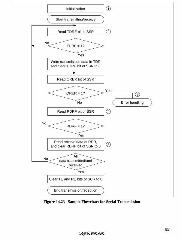
531
Start transmitting/receive
Initialization
Read TDRE bit in SSR
Alldata transmitted/and
received
End transmission/reception
1
2
No
Yes
TDRE = 1?
Write transmission data in TDRand clear TDRE bit of SSR to 0
RDRF = 1?
Yes
No
Clear TE and RE bits of SCR to 0
Yes
No
Read ORER bit of SSR
Error handling
3ORER = 1?Yes
Read receive data of RDR,and clear RDRF bit of SSR to 0
Read RDRF bit of SSR 4
5
No
Figure 14.23 Sample Flowchart for Serial Transmission

532
14.4 SCI Interrupt Sources and the DMAC/DTC
The SCI has four interrupt sources: transmit-end (TEI), receive-error (ERI), receive-data-full(RxI), and transmit-data-empty (TxI). Table 14.12 lists the interrupt sources and indicates theirpriority. These interrupts can be enabled and disabled by the TIE, RIE, and TEIE bits in the serialcontrol register (SCR). Each interrupt request is sent separately to the interrupt controller.
TxI is requested when the TDRE bit in the SSR is set to 1. TxI can start the direct memory accesscontroller (DMAC) or the data transfer controller (DTC) to transfer data. TDRE is automaticallycleared to 0 when the DMAC or the DTC writes data in the transmit data register (TDR).
RxI is requested when the RDRF bit in the SSR is set to 1. RxI can start the DMAC or the DTC totransfer data. RDRF is automatically cleared to 0 when the DMAC or the DTC reads the receivedata register (RDR).
ERI is requested when the ORER, PER, or FER bit in the SSR is set to 1. ERI cannot start theDMAC or the DTC.
TEI is requested when the TEND bit in the SSR is set to 1. TEI cannot start the DMAC or theDTC. Where the TxI interrupt indicates that transmit data writing is enabled, the TEI interruptindicates that the transmit operation is complete.
Table 14.12 SCI Interrupt Sources
Interrupt Source Description DMAC/DTC Activation Priority
ERI Receive error (ORER, PER, or FER) No High
RxI Receive data full (RDRF) Yes
TxI Transmit data empty (TDRE) Yes
TEI Transmit end (TEND) No Low

533
14.5 Notes on Use
Sections 14.5.1 through 14.5.9 provide information for using the SCI.
14.5.1 TDR Write and TDRE Flags
The TDRE bit in the serial status register (SSR) is a status flag indicating loading of transmit datafrom TDR into TSR. The SCI sets TDRE to 1 when it transfers data from TDR to TSR. Data canbe written to TDR regardless of the TDRE bit status. If new data is written in TDR when TDRE is0, however, the old data stored in TDR will be lost because the data has not yet been transferred tothe TSR. Before writing transmit data to the TDR, be sure to check that TDRE is set to 1.
14.5.2 Simultaneous Multiple Receive Errors
Table 14.13 indicates the state of the SSR status flags when multiple receive errors occursimultaneously. When an overrun error occurs, the RSR contents cannot be transferred to theRDR, so receive data is lost.
Table 14.13 SSR Status Flags and Transfer of Receive Data
SSR Status FlagsReceive DataTransfer
Receive Error Status RDRF ORER FER PER RSR → RDR
Overrun error 1 1 0 0 X
Framing error 0 0 1 0 O
Parity error 0 0 0 1 O
Overrun error + framing error 1 1 1 0 X
Overrun error + parity error 1 1 0 1 X
Framing error + parity error 0 0 1 1 O
Overrun error + framing error + parityerror
1 1 1 1 X
Notes: O = Receive data is transferred from RSR to RDR.X = Receive data is not transferred from RSR to RDR.
534
14.5.3 Break Detection and Processing
Break signals can be detected by reading the RxD pin directly when a framing error (FER) isdetected. In the break state, the input from the RxD pin consists of all 0s, so FER is set and theparity error flag (PER) may also be set. In the break state, the SCI receiver continues to operate, soif the FER bit is cleared to 0, it will be set to 1 again.
14.5.4 Sending a Break Signal
The TxD pin becomes a general I/O pin with the I/O direction and level determined by the I/O portdata register (DR) and pin function controller (PFC) control register (CR). These conditions allowbreak signals to be sent. The DR value is substituted for the marking status until the PFC is set.Consequently, the output port is set to initially output a 1. To send a break in serial transmission,first clear the DR to 0, then establish the TxD pin as an output port using the PFC. When TE iscleared to 0, the transmission section is initialized regardless of the present transmission status.
14.5.5 Receive Error Flags and Transmitter Operation (Clock Synchronous Mode Only)
When a receive error flag (ORER, PER, or FER) is set to 1, the SCI will not start transmittingeven if TDRE is set to 1. Be sure to clear the receive error flags to 0 before starting to transmit.Note that clearing RE to 0 does not clear the receive error flags.
14.5.6 Receive Data Sampling Timing and Receive Margin in the Asynchronous Mode
In the asynchronous mode, the SCI operates on a base clock of 16 times the bit rate frequency. Inreceiving, the SCI synchronizes internally with the falling edge of the start bit, which it samples onthe base clock. Receive data is latched on the rising edge of the eighth base clock pulse (figure14.24).

535
0 7 8 15 0 7 8 15 0 5Internalbase clock
Receivedata (RxD)
Synchronizationsampling timing
Datasampling timing
8 clocks16 clocks
Start bit
–7.5 clocks +7.5 clocks
D0 D1
Figure 14.24 Receive Data Sampling Timing in Asynchronous Mode
The receive margin in the asynchronous mode can therefore be expressed as:
M = 0.5 – 1
2N – L – 0.5 F –
D – 0.5
N1 + F 100%
( ) ( ) ×
M : Receive margin (%)N : Ratio of clock frequency to bit rate (N = 16)D : Clock duty cycle (D = 0–1.0)L : Frame length (L = 9–12)F : Absolute deviation of clock frequency
From the equation above, if F = 0 and D = 0.5 the receive margin is 46.875%:
D = 0.5, F = 0M = (0.5 – 1/(2 × 16)) × 100%
= 46.875%
This is a theoretical value. A reasonable margin to allow in system designs is 20–30%.

536
14.5.7 Constraints on DMAC/DTC Use
• When using an external clock source for the synchronization clock, update the TDR with theDMAC or the DTC, and then after five system clocks or more elapse, input a transmit clock. Ifa transmit clock is input in the first four system clocks after the TDR is written, an error mayoccur (figure 14.25).
• Before reading the receive data register (RDR) with the DMAC/DTC, select the receive-data-full interrupt of the SCI as a start-up source.
D0 D1 D2 D3 D4 D5 D6 D7
SCK
TDRE
t
Note: During external clock operation, an error may occur if t is 4φ or less.
Figure 14.25 Example of Clock Synchronous Transmission with DMAC
14.5.8 Cautions for Clock Synchronous External Clock Mode
• Set TE = RE = 1 only when the external clock SCK is 1.
• Do not set TE = RE = 1 until at least four clocks after the external clock SCK has changedfrom 0 to 1.
• When receiving, RDRF is 1 when RE is set to zero 2.5–3.5 clocks after the rising edge of theRxD D7 bit SCK input, but it cannot be copied to RDR.
14.5.9 Caution for Clock Synchronous Internal Clock Mode
When receiving, RDRF is 1 when RE is set to zero 1.5 clocks after the rising edge of the RxD D7bit SCK output, but it cannot be copied to RDR.

537
Section 15 High Speed A/D Converter (Excluding A Mask)
15.1 Overview
The high speed A/D converter has 10-bit resolution, and can select from a maximum of eightchannels of analog inputs.
15.1.1 Features
The high speed A/D converter has the following features:
• 10-bit resolution
• Eight input channels
• Analog conversion voltage range setting is selectable
Using the reference voltage pin (AVref) as an analog standard voltage (Vref), conversion ofanalog input from 0 to Vref (only with SH7043).
• High-speed conversion
Minimum conversion time: 2.9 µs per channel (for 28-MHz operation)
1.4 µs per channel during continuous conversion
• Multiple conversion modes
Select mode/group mode
Single mode/scan mode
Buffered operation possible
2 channel simultaneous sampling possible
• Three types of conversion start
Software, timer conversion start trigger (MTU), or ADTRG pin can be selected.
• Eight data registers
Conversion results stored in 16-bit data registers corresponding to each channel.
• Sample and hold function
• A/D conversion end interrupt generation
An A/D conversion end interrupt (ADI) request can be generated on completion of A/Dconversions

538
15.1.2 Block Diagram
Figure 15.1 is the block diagram of the high speed A/D converter.
+−
AVccAVref*
AVss
AN0
AN1
AN2
AN3
AN4
AN5
AN6
ADTRG
AN7
D/Aconversion
circuit
S&H A
S&H B
ADDRA
ADDRB
ADDRC
ADDRD
ADDRE
ADDRF
ADDRG
ADDRH
ADCR ADCSR
Internaldata bus
Bus I/F
Interrupt signalADI
8-bit timer orMTU conversionstart trigger
CMP
Mod
ule
inte
rnal
dat
a bu
s
Con
trol
logi
c
Mul
tiple
xer
ADCR:ADSCR:ADDRA:ADDRB:ADDRC:ADDRD:
A/D control registerA/D control status registerA/D data register AA/D data register BA/D data register CA/D data register D
CMP:S&H:
ADDRE:ADDRF:ADDRG:ADDRH:
Comparator arraySample and hold circuitA/D data register EA/D data register FA/D data register GA/D data register H
Note: * SH7043 only
Figure 15.1 High Speed A/D Converter Block Diagram
15.1.3 Pin Configuration
Table 15.1 shows the input pins used by the high speed A/D converter.
The AVcc and AVss pins are for the A/D converter internal analog section power supply. TheAVref pin is for the A/D conversion standard voltage.

539
Table 15.1 Pin Configuration
Pin Abbreviation I/O Function
Analog supply AVCC I Analog section power supply
Analog ground AVSS I Analog section ground and A/D conversionreference voltage
Reference voltage AVref I A/D conversion standard voltage(SH7043 only)
Analog input 0 AN0 I Analog input channel 0
Analog input 1 AN1 I Analog input channel 1
Analog input 2 AN2 I Analog input channel 2
Analog input 3 AN3 I Analog input channel 3
Analog input 4 AN4 I Analog input channel 4
Analog input 5 AN5 I Analog input channel 5
Analog input 6 AN6 I Analog input channel 6
Analog input 7 AN7 I Analog input channel 7
A/D external trigger input ADTRG I External trigger for A/D conversion start
15.1.4 Register Configuration
Table 15.2 shows the configuration of the high speed A/D converter registers.
Table 15.2 Register Configuration
Name Abbreviation R/W Initial Value Address Access Size
A/D data register A ADDRA R H'0000 H'FFFF83F0 8,16
A/D data register B ADDRB R H'0000 H'FFFF83F2
A/D data register C ADDRC R H'0000 H'FFFF83F4
A/D data register D ADDRD R H'0000 H'FFFF83F6
A/D data register E ADDRE R H'0000 H'FFFF83F8
A/D data register F ADDRF R H'0000 H'FFFF83FA
A/D data register G ADDRG R H'0000 H'FFFF83FC
A/D data register H ADDRH R H'0000 H'FFFF83FE
A/D control/status register ADCSR R/(W)* H'00 H'FFFF83E0
A/D control register ADCR R/W H'00 H'FFFF83E1
Note: * Only 0 can be written to bit 7 to clear the flag.

540
15.2 Register Descriptions
15.2.1 A/D Data Registers A–H (ADDRA–ADDRH)
The ADDR are 16-bit read only registers for storing A/D conversion results. There are eight ofthese registers, ADDRA through ADDRH.
The A/D converted data is 10-bit data which is sent to the ADDR for the corresponding convertedchannel for storage. The lower 8 bits of the A/D converted data are transferred to and stored in thelower byte (bits 7–0) of the ADDR, and the upper 2 bits are stored into the upper byte (bits 9, 8).Bits 15–10 always read as 0. Data reads can be either byte or word. The upper 8 bits of theconverted data are transferred upon byte data reads. Additionally, buffered operation is possible bycombining ADDRA–ADDRD.
Table 15.3 shows the correspondence between the analog input channels and the ADDR.
The ADDR are initialized to H'0000 by power-on reset or in standby mode. Manual reset does notinitialize ADDR.
Bit: 15 14 13 12 11 10 9 8
— — — — — — AD9 AD8
Initial value: 0 0 0 0 0 0 0 0
R/W: R R R R R R R R
Bit: 7 6 5 4 3 2 1 0
AD7 AD6 AD5 AD4 AD3 AD2 AD1 AD0
Initial value: 0 0 0 0 0 0 0 0
R/W: R R R R R R R R

541
Table 15.3 Analog Input Channel and ADDR Correspondence
Analog Input Channel A/D Data Register
AN0 ADDRA*
AN1 ADDRB*
AN2 ADDRC*
AN3 ADDRD*
AN4 ADDRE
AN5 ADDRF
AN6 ADDRG
AN7 ADDRH
Note: * Except during buffer operation
15.2.2 A/D Control/Status Register (ADCSR)
The ADCSR is an 8-bit read/write register used for A/D conversion operation control and toindicate status.
The ADCSR is initialized to H'00 by power-on reset or in standby mode. Manual reset does notinitialize ADCSR.
Bit: 7 6 5 4 3 2 1 0
ADF ADIE ADST CKS GRP CH2 CH1 CH0
Initial value: 0 0 0 0 0 0 0 0
R/W: R/(W)* R/W R/W R/W R/W R/W R/W R/W
Note: * The only value that can be written is a 0 to clear the flag.

542
• Bit 7—A/D End Flag (ADF): This status flag indicates that A/D conversion has ended.
Bit 7: ADF Description
0 Clear conditions (initial value)
• With ADF = 1, by reading the ADF flag then writing 0 in ADF
• When the DTC or DMAC are activated by an ADI interrupt
1 Set conditions
• Single mode: When A/D conversion ends after conversion for alldesignated channels (during buffer operation, this is not set untiloperation of the specified buffer has ended)
• Scan mode: After one round of A/D conversion for all specifiedchannels
• Bit 6—A/D Interrupt Enable (ADIE): Enables or disables interrupt requests (ADI) after A/Dconversion ends. Set the ADIE bit while conversion is suspended.
Bit 6: ADIE Description
0 Disables interrupt requests (ADI) after A/D conversion ends (initialvalue)
1 Enables interrupt requests (ADI) after A/D conversion ends
• Bit 5—A/D Start (ADST): Selects start or stop for A/D conversion. A 1 is maintained duringA/D conversions.
The ADST bit can be set to 1 by software, timer conversion start triggers, or an A/D externaltrigger input pin (ADTRG).
Bit 5: ADST Description
0 A/D conversion halted (initial value)
1 Single mode: Start A/D conversion. Automatically cleared to 0 afterconversion for the designated channel ends.
Scan mode: Start A/D conversion. Continuous conversion until 0cleared by software.

543
• Bit 4—Clock Select (CKS): Sets the A/D conversion time. Set, according to the operatingfrequency, to give a conversion time of at least 2 µs (5 V version) or 4 µs (3.3 V version).
Make conversion time changes only while conversion is halted.
Bit 4: CKS Description
0 Conversion time = 40 states (A/D converter standard clock = φ/2) (initialvalue)
1 Conversion time = 80 states (when φ/4 is selected)
• Bit 3—Group Mode (GRP): Designates either select mode or group mode for the A/Dconversion channel selection.
Set the GRP bit only while conversion is halted.
Bit 3: GRP Description
0 Select mode (initial value)
1 Group mode
• Bits 2–0—Channel Select 2–0 (CH2–CH0): These bits, along with the GRP bit, select theanalog input channel.
Set the input channel only while conversion is halted.
Description
Bit 2: CH2 Bit 1: CH1 Bit 0: CH0 Select Mode (GRP = 0) Group Mode (GRP = 1)
0 0 0 AN0 (initial value) AN0
0 0 1 AN1 AN0–AN1
0 1 0 AN2 AN0–AN2
0 1 1 AN3 AN0–AN3
1 0 0 AN4 AN0–AN4
1 0 1 AN5 AN0–AN5
1 1 0 AN6 AN0–AN6
1 1 1 AN7 AN0–AN7

544
15.2.3 A/D Control Register (ADCR)
The ADCR is an 8-bit read/write register used for A/D conversion operation control. The ADCR isinitialized to H'00 by power-on reset or in standby mode. Manual reset does not initialize.
Bit: 7 6 5 4 3 2 1 0
— PWR TRGS1 TRGS0 SCAN DSMP BUFE1 BUFE0
Initial value: 0 0 0 0 0 0 0 0
R/W: R R/W R/W R/W R/W R/W R/W R/W
• Bit 7—Reserved: This bit always reads as 0. The write value should always be 0.
• Bit 6—Power (PWR): Designates the conversion start mode for the high speed A/D converter.Setting the PWR bit to 1 sets high speed start mode, and a 0 sets to low power conversionmode. See section 15.4.7, Conversion Start Modes, for details on the conversion startoperation.
Set the PWR bit only while conversion is halted.
Bit 6: PWR Description
0 Low power conversion mode (initial value)
1 High speed start mode
• Bits 5 and 4—Timer Trigger Select 1, 0 (TRGS1, TRGS0): These bits enable or prohibit A/Dconversion starts by trigger signals.
Set the TRGS1, TRGS0 bits only while conversion is halted.
Bit 5: TRGS1 Bit 4: TRGS0 Description
0 0 Enable A/D conversion start by software (initial value)
0 1 Enables A/D conversion start by MTU conversion start trigger
1 0 Reserved
1 1 Enables A/D conversion start by external trigger pin (ADTRG)
• Bit 3—Scan Mode (SCAN): Selects either single mode or scan mode for the A/D conversionoperation mode. See section 15.4, Operation, for details on single mode and scan modeoperation.
Set the SCAN bit only while conversion is halted.
Bit 3: SCAN Description
0 Single mode (initial value)
1 Scan mode

545
• Bit 2—Simultaneous Sampling (DSMP): Enables or disables the simultaneous sampling of twochannels. See section 15.4.6, Simultaneous Sampling Operation, for details on simultaneoussampling.
Set the DSMP bit only while conversion is halted.
Bit 2: DSMP Description
0 Normal sampling operation (initial value)
1 Simultaneous sampling operation
• Bits 1–0—Buffer Enable 1, 0 (BUFE1, BUFE0): These bits select whether to use theADDRB–ADDRD as buffer registers.
Set the BUFE1 and BUFE0 bits only while conversion is halted.
Bit 1: BUFE1 Bit 0: BUFE0 Description
0 0 Normal operation (initial value)
0 1 ADDRA and ADDRB buffer operation: conversion result →ADDRA → ADDRB (ADDRB is the buffer register)
1 0 ADDRA and ADDRC, also ADDRB and ADDRD bufferoperation: conversion result 1 → ADDRA → ADDRC,conversion result 2 → ADDRB → ADDRD (ADDRC andADDRD are buffer registers)
1 1 ADDRA–ADDRD buffer operation: conversion result →ADDRA → ADDRB → ADDRC → ADDRD (ADDRB–ADDRDare buffer registers)
15.3 Bus Master Interface
The ADDRA–ADDRH are 16-bit registers with a 16-bit width data bus to the bus master. The busmaster can read from ADDRA–ADDRH in either word or byte units.
When an ADDR is read in word units, the ADDR contents are transferred to the bus master 16 bitsat a time. In byte unit reads, the contents of the most significant eight bits (AD9–AD2) of theconverted data (AD9–AD0) are transferred to the bus master.
Figures 15.2 and 15.3 shows an example of the ADDR read operation.

546
0
0
0
0
0
0
AD 9
AD 8
AD 7
AD 6
AD 5
AD 4
AD 3
AD 2
AD 1
AD 0
Upper 8 bits
Internal data bus
Bus I/FData
register
Word data read
Lower 8 bits
Figure 15.2 ADDR Read Operation (1)

547
0
0
0
0
0
0
AD 9
AD 8
AD 7
AD 6
AD 5
AD 4
AD 3
AD 2
AD 1
AD 0
Upper 8 bits
Internal data bus
Bus I/FByte data readData register
Figure 15.3 ADDR Read Operation (2)

548
15.4 Operation
• The high speed A/D converter has 10-bit resolution.
• In addition to the four operating modes of select or group, and single or scan can be set incombination with buffer operation and simultaneous sampling operation.
• Select mode uses one channel and group mode selects multiple channels.
• One start in the single mode performs conversions on all selected channels, and one start in thescan mode performs repeated conversions until stopped by software.
• In buffer operation, the previous conversion result is saved in a buffer register at the end of aconversion for the relevant channel.
• In simultaneous sampling operation, the analog input voltages of two channels are sampledsimultaneously then converted in order.
• Software, a timer conversion start trigger (MTU), or an ADTRG input can be selected as theconversion start condition.
• High speed start mode or low power conversion mode can be selected for A/D conversionusing the PWR bit setting.
• When changing the operation mode or input channel, rewrite the ADCSR, ADCR while theADST bit is cleared to 0. After rewriting the ADCSR, ADCR, A/D conversion will be restartedwhen the ADST bit is set to 1. Operation mode or input channel changes can be madesimultaneously with ADST bit setting. When stopping an A/D conversion before completion, 0clear the ADST bit.
15.4.1 Select-Single Mode
Choose select-single mode when doing A/D conversions for one channel only.
When the ADST bit is set to 1, A/D conversion is started according to the designated conversionstart conditions. The ADST bit is held to 1 during the A/D conversion and is automatically clearedto 0 upon completion.
The ADF flag is also set to 1 at the end of conversion. If the ADIE bit is set to 1 at this time, anADI interrupt request is generated. The ADF flag is cleared by reading the ADCSR, then writing a0.
Figure 15.4 shows an example of operation in the select-single mode when AN1 is selected.

549
ADDRB
ADDRA
Channel 3
Channel 2
Channel 1
Channel 0
ADST
ADF
ADDRC
ADDRD
Automatic clear
Sampling 1Conversion
standbyConversion
standby
Conversion standby
Conversion standby
Conversion standby
A/Dconversion 1
Conversion result 1
Set to 1 by software
Figure 15.4 A/D Converter Operation Example (Select-Single Mode)
15.4.2 Select-Scan Mode
Choose select-scan mode when doing repeated A/D conversions for one channel. This is usefulwhen doing continuous monitoring of the analog input of one channel.
When the ADST bit is set to 1, A/D conversion is started according to the designated conversionstart conditions. The ADST bit is held to 1 until 0 cleared by software. A/D conversion for theselected input channel is repeated during that interval.
The ADF flag is set to 1 at the end of the first conversion. At this point, if the ADIE bit is set, anADI interrupt request is issued, and the A/D converter is halted. With the A/D converter in stopmode due to an ADI interrupt request, conversion is restarted when the ADF flag is cleared to 0.The ADF flag is cleared by reading the ADCSR then writing a 0.
Figure 15.5 shows an example of operation in the select-scan mode when AN1 is selected.

550
ADDRB
ADDRA
Channel 3
Channel 2
Channel 1
Channel 0
ADST
ADF
ADDRC
ADDRD
Sampling3
Sampling 6
A/D conversion 5
Sampling1
A/Dconver-sion 1
A/Dconver-sion 3
Conver-sion
standby
A/Dconver-sion 2
Sampling2
Sampling4
Sampling5
A/Dconver-sion 4
Conversionstandby
Conversion standby
Set to 1 by software Cleared to 0 by software
Conversion standby
Conversion standby
Conversionstopped
Conver-sion
result 1
Conver-sion
result 2
Conver-sion
result 3
Conver-sion
result 4
Figure 15.5 A/D Converter Operation Example (Select-Scan Mode)
15.4.3 Group-Single Mode
Choose group-single mode when doing A/D conversions for multiple channels.
When the ADST bit is set to 1, A/D conversion is started according to the designated conversionstart conditions. The ADST bit is held to 1 during A/D conversion and is automatically cleared to0 when all conversions for the designated input channels are completed.
The ADF flag is set to 1 when all conversions for the designated input channels are completed. Ifthe ADIE bit is set to 1 at this time, an ADI interrupt request is generated. The ADF flag is clearedby reading the ADCSR then writing a 0.
Figure 15.6 shows an example of operation in the group-single mode when AN0–AN2 areselected.

551
ADDRB
ADDRA
Channel 3
Channel 2
Channel 1
Channel 0
ADST
ADF
ADDRC
ADDRD
Sampling1
Sampling2
Sampling3
A/Dconversion
1
A/Dconversion
2
A/Dconversion
3
Conversion standby
Conversion standby
Conversion standby
Conversion standby
Conversionstandby
Conversionstandby
Conversionstandby
Automatic clearSet to 1 by software
Conversion result 1
Conversion result 2
Conversion result 3
Figure 15.6 A/D Converter Operation Example (Group-Single Mode)
15.4.4 Group-Scan Mode
Choose group-scan mode when doing repeated A/D conversions for multiple channels. This isuseful when doing continuous monitoring of the analog inputs of multiple channels.
When the ADST bit is set to 1, A/D conversion is started according to the designated conversionstart conditions. The ADST bit is held to 1 until 0 cleared by software. A/D conversion for theselected input channels is repeated during that interval.
The ADF flag is set to 1 at the completion of the first conversions of all the designated inputchannels. At this point, if the ADIE bit is set to 1, an ADI interrupt request is issued, and the A/Dconverter is temporarily halted. With the A/D converter in stop mode due to an ADI interruptrequest, conversion is restarted when the ADF flag is cleared to 0. The ADF flag is cleared byreading the ADCSR, then writing a 0.

552
Figure 15.7 shows an example of operation in the group-scan mode when AN0–AN2 are selected.
ADDRB
ADDRA
Channel 3
Channel 2
Channel 1
Channel 0
ADST
ADF
ADDRC
ADDRD
Sam-pling
1
Sam-pling
4
Sam-pling
2
Conver-sion
standby
Conversion standby
Sam-pling
5
Sam-pling
3
Sam-pling
6
A/Dconver-sion 1
A/Dconver-sion 4
A/Dconver-sion 2
A/Dconver-sion 5
A/Dconver-sion 3
Conversionstandby
Conversion standby
Conversion standby
Conver-sion
standby
Conver-sion
standby
Cleared to 0 by softwareSet to 1 by software
Conversion result 1 Conversion result 4
Conversion result 5
Conversion result 2
Conversion result 3
Conver-sion
stopped
Figure 15.7 A/D Converter Operation Example (Group-Scan Mode)
15.4.5 Buffer Operation
When conversion ends on the relevant channel, the conversion result is stored in the ADDR, andsimultaneously, the previously stored result is transferred to another ADDR. Buffer operation canbe selected from the following:
• AN0 → ADDRA → ADDRB (Two-stage, one-group operation)
• AN0 → ADDRA → ADDRC, AN1 → ADDRB → ADDRD (Two-stage, two-groupoperation)
• AN0 → ADDRA → ADDRB → ADDRC → ADDRD (Four-stage, one-group operation)

553
To use in combination with simultaneous sampling, set GRP = 1, BUFE1, BUFE0 = B'10, andCH2 = 0. Buffer operation timing is shown in figure 15.8.
ADDRB
ADDRA
Channel 1
Channel 0
ADST
ADF
ADDRD
ADDRC
Channel 2
Channel 3
Sampling1
Sampling3
Sampling2
Sampling4
Sampling5
A/Dconver-sion 1
A/Dconver-sion 3
A/Dconver-sion 2
A/Dconver-sion 4
Conversionstandby
Conversion standby
Conversion standby
Conversion standby
Conver-sion
standby
Cleared to 0by software
Set to 1by software
Conver-sion
result 1
Conver-sion
result 2
Conver-sion
result 3
Conver-sion
result 4
Conver-sion
result 1
Conver-sion
result 2
Conver-sion
result 3
Figure 15.8 Buffer Operation Example (Select Scan Mode: Two-Stage One-GroupOperation, When CH2–CH0 = B'001)
Buffer-Only Operation: When performing conversion only on the analog input channelsspecified by the BUFE1 and BUFE0 bits, select group mode, and you can select the ADF flagsetting conditions with the CH2–CH0 bits.
Table 15.4 shows conversion during buffer operation and ADF flag setting conditions. The ADFflag is set at the point in the table when the final conversion has ended. In single mode, conversionis halted after the ADF flag is set to 1. In scan mode, conversion continues, and the converted datais stored in sequence in the buffer registers specified by the BUFE1 and BUFE0 bits.
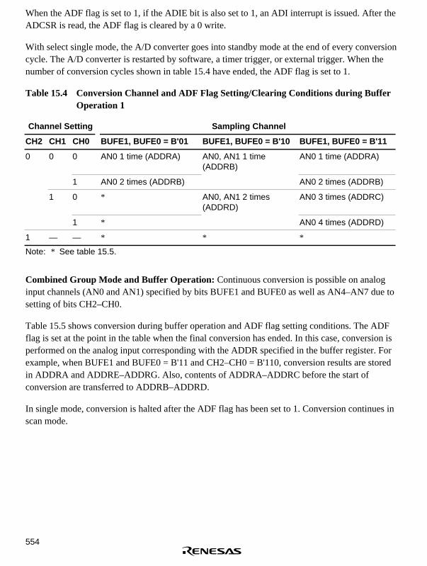
554
When the ADF flag is set to 1, if the ADIE bit is also set to 1, an ADI interrupt is issued. After theADCSR is read, the ADF flag is cleared by a 0 write.
With select single mode, the A/D converter goes into standby mode at the end of every conversioncycle. The A/D converter is restarted by software, a timer trigger, or external trigger. When thenumber of conversion cycles shown in table 15.4 have ended, the ADF flag is set to 1.
Table 15.4 Conversion Channel and ADF Flag Setting/Clearing Conditions during BufferOperation 1
Channel Setting Sampling Channel
CH2 CH1 CH0 BUFE1, BUFE0 = B'01 BUFE1, BUFE0 = B'10 BUFE1, BUFE0 = B'11
0 0 0 AN0 1 time (ADDRA) AN0, AN1 1 time(ADDRB)
AN0 1 time (ADDRA)
1 AN0 2 times (ADDRB) AN0 2 times (ADDRB)
1 0 * AN0, AN1 2 times(ADDRD)
AN0 3 times (ADDRC)
1 * AN0 4 times (ADDRD)
1 — — * * *
Note: * See table 15.5.
Combined Group Mode and Buffer Operation: Continuous conversion is possible on analoginput channels (AN0 and AN1) specified by bits BUFE1 and BUFE0 as well as AN4–AN7 due tosetting of bits CH2–CH0.
Table 15.5 shows conversion during buffer operation and ADF flag setting conditions. The ADFflag is set at the point in the table when the final conversion has ended. In this case, conversion isperformed on the analog input corresponding with the ADDR specified in the buffer register. Forexample, when BUFE1 and BUFE0 = B'11 and CH2–CH0 = B'110, conversion results are storedin ADDRA and ADDRE–ADDRG. Also, contents of ADDRA–ADDRC before the start ofconversion are transferred to ADDRB–ADDRD.
In single mode, conversion is halted after the ADF flag has been set to 1. Conversion continues inscan mode.

555
Table 15.5 Conversion Channel and ADF Flag Setting/Clearing Conditions During BufferOperation 2
Channel Setting Sampling Channel
CH2 CH1 CH0 BUFE1, BUFE0 = B'01 BUFE1, BUFE0 = B'10 BUFE1, BUFE0 = B'11
0 0 — * * *
1 0 AN0, AN2 (ADDRC)
1 AN0, AN2, AN3(ADDRD)
1 0 0 AN0, AN2–AN4(ADDRE)
AN0, AN1, AN4(ADDRE)
AN0, AN4 (ADDRE)
1 AN0, AN2–AN5(ADDRF)
AN0, AN1, AN4, AN5(ADDRF)
AN0, AN4, AN5(ADDRF)
1 0 AN0, AN2–AN6(ADDRG)
AN0, AN1, AN4–AN6(ADDRG)
AN0, AN4–AN6(ADDRG)
1 AN0, AN2–AN7(ADDRH)
AN0, AN1, AN4–AN7(ADDRH)
AN0, AN4–AN7(ADDRH)
Note: * See table 15.4.
ADF Flag Clearing: When the DTC and DMAC are started up due to an A/D conversion endinterrupt, the ADF flag is cleared when the ADDR specified in table 15.4 or 15.5 has been read.
Resetting the Number of Buffer Operations: Clear the BUFE1 and BUFE0 bits to B'00 inconversion standby mode or when the converter has been halted. The number of buffer operationsis cleared to 0.
Updating Buffer Operations: Clear the BUFE1 and BUFE0 bits to B'00 in conversion standbymode or when the converter has been halted. Thereafter, set BUFE1 and BUFE0, and the bufferoperations shown in tables 15.4 and 15.5 are performed when conversion is resumed.
15.4.6 Simultaneous Sampling Operation
With simultaneous sampling, continuous conversion is conducted with sampling of the inputvoltages on two channels at the same time. Simultaneous sampling is valid in group mode.Channels for sampling are determined by the CH2 and CH1 bits of the RDSCR. The combinationsare shown in table 15.6. For example, if GRP = 1 when CH2 and CH1 = B'11, sampling occurs inorder in the following pairs: AN0, AN1→AN2, AN3→AN4, AN5→AN6, AN7. Sampling timingis shown in figure 15.9.
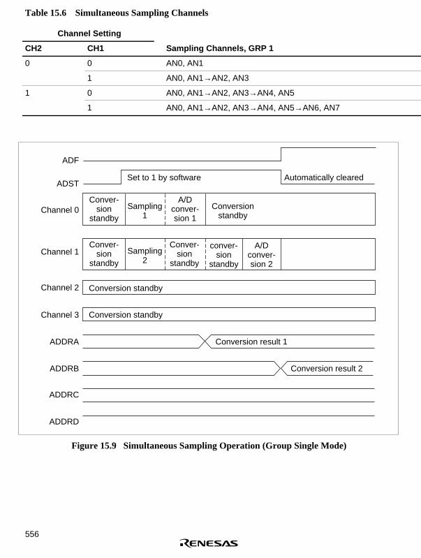
556
Table 15.6 Simultaneous Sampling Channels
Channel Setting
CH2 CH1 Sampling Channels, GRP 1
0 0 AN0, AN1
1 AN0, AN1→AN2, AN3
1 0 AN0, AN1→AN2, AN3→AN4, AN5
1 AN0, AN1→AN2, AN3→AN4, AN5→AN6, AN7
ADDRB
ADDRA
ADST
ADF
ADDRD
ADDRC
Automatically cleared
Channel 0
Channel 1
Channel 2
Channel 3
Sampling1
A/Dconver-sion 1
A/Dconver-sion 2
conver-sion
standby
Conversionstandby
Conversion standby
Conversion standby
Conver-sion
standby
Sampling2
Conver-sion
standby
Conver-sion
standby
Set to 1 by software
Conversion result 1
Conversion result 2
Figure 15.9 Simultaneous Sampling Operation (Group Single Mode)

557
15.4.7 Conversion Start Modes
The conversion start mode of the high speed A/D converter is set by the PWR bit of the ADCSR.When the PWR bit is cleared to 0, low-power conversion mode is set and the internal analogcircuit becomes inactive. High-speed start mode is set by setting the PWR bit to 1, and the analogcircuit becomes active.
In the low-power conversion mode, power is applied to the analog circuitry simultaneous to theconversion start (ADST set). When 200 cycles of the reference clock have elapsed, conversionbecomes possible for the analog circuit and the first A/D conversion begins. When performingconsecutive conversions, the second and later conversions are executed in 10 cycles. Select thebasic clock with the CKS bit of the ADCSR. When the A/D conversion ends, ADST is cleared to0 and the analog circuit power supply is automatically cut off. Because the analog circuit is onlyactive during the A/D conversion operation period in this mode, current consumption can bereduced.
In high-speed start mode, ADST is cleared to 0 when A/D conversion ends. Power continues to besupplied to the analog circuitry, and conversion-ready status is maintained. Conversion is restartedimmediately by resetting ADST to 1. However, the first conversion after power-on begins 200cycles after setting ADST. Clear the PWR bit to 0 to switch off the analog power supply. Whenperforming consecutive conversions, the second and later conversions are executed in 20 cycles.Because the analog circuit is always active in this mode, A/D conversion can be executed at highspeed.

558
Figures 15.10 and 15.11 show examples of conversion start operation timing.
ADDRB
ADDRA
Channel 0
Channel 1
Channel 2
Channel 3
ADST
ADF
ADDRD
ADDRC
Set to 1 by software
Analog circuitpower supply
200 cycles
Set Clear
Sam-pling
1
Sam-pling
2
Sam-pling
3
A/Dconver-sion 1
A/Dconver-sion 2
A/Dconver-sion 3
Conver-sion
standby
Conver-sion
standby
Conver-sion
standby
Conver-sion
standby
Cleared to 0 by software
Conversionresult 1
Conversionresult 2
Conversionresult 3
Figure 15.10 Conversion Start Operation (Low-Power Conversion Mode)

559
ADDRB
ADDRA
Channel 1
Channel 0
ADST
ADF
ADDRD
ADDRC
Set to 1 by software
Analogcircuitpowersupply
Switched offby software
Channel 2
Channel 3
Set to 1 by software
Sam-pling
1
Sam-pling
2
A/Dconver-sion 1
A/Dconver-sion 2
Conversion result 1
Conversion result 2
Conversionstandby
Conversionstandby
Conversionstandby
Conversionstandby
200 cycles
Switched on by software (PWR set to 1)
(PWR cleared to 0)
Figure 15.11 Conversion Start Operation (High-Speed Start Mode)

560
15.4.8 Conversion Start by External Input
A/D conversions can be started by trigger signals generated by timer conversion start triggers orADTRG inputs. When a trigger signal designated by the TRGS1 and TRGS0 bits of the ADCRoccurs, the ADST bit of the ADCSR is set to 1 and A/D conversion is started.
The other operations are the same as when the ADST bit is set to 1 by software. Figure 15.12shows an example of the timing when the ADST bit is set by an external input.
ADDRB
ADDRA
ADST
ADDRD
ADDRC
ADF
Set
ADTRG(external
trigger)
Channel 0
Channel 1
Channel 2
Channel 3
Sam-pling 1
A/Dconver-sion 1
Conver-sion
standby
Conversionstandby
Conversion standby
Conversion standby
Conversion standby
Conversion result 1
Figure 15.12 Conversion Start by ADTRG Conversion Start Trigger

561
15.4.9 A/D Conversion Time
The high speed A/D converter has an on-chip sample and hold circuit. The high speed A/Dconverter samples the input at time tD after the ADST bit is set to 1, and then starts the conversion.
The A/D conversion time tCONV is the sum of the conversion start delay time tD, the input samplingtime tSPL, and the operating time tCP. This conversion time is not a set value, but is decided by thetD ADCSR write timing, or the timer conversion start trigger generation timing.
Figure 15.13 shows an example of A/D conversion timing. Table 15.7 lists A/D conversion times.
Address
Write signal
ADST
Samplingtiming
φ
ADF
tD
tCONV
tSPL tCP
t D:t SPL:
t CONV:t CP:
A/D conversion start delay timeInput sampling timeA/D conversion timeOperation time
Figure 15.13 A/D Conversion Timing

562
Table 15.7 A/D Conversion Times
CKS = 0 CKS = 1
Time Symbol Min Typ Max Min Typ Max
A/D conversion startdelay time
tD 1.5 1.5 1.5 1.5 1.5 1.5
Input sampling time tSPL 20 20 20 40 40 40
A/D conversion time tCONV 42.5 42.5 42.5 82.5 82.5 82.5
Notes: 1. Unit: states2. Table entries are for when ADST = 1. If 200 states have not elapsed since the PWR bit
has been set, no conversions are done until after those 200 states have occurred.When PWR = 0, add 200 states to the first A/D conversion start delay time. Whencontinuously executing conversion, tcp for the second time and following is 20 cyclewhen CKS=0 and 40 cycle when CKS=1.
The CKS bit of the ADCSR is the operation time tCONV, but set so that this is 2 µs or greater. Table15.8 shows the operating frequency and CKS bit settings.
Table 15.8 Operating Frequency and CKS Bit Settings
Conversion Time Minimum Conversion Time (µs)
CKS (States) 28 MHz 20 MHz 16 MHz 10 MHz 8 MHz
0 42.5 — 2.1 2.6 4.3 5.3
1 82.5 2.9 4.2 5.0 8.3 10.3
Note: The indication “—” means the setting is not available.
15.5 Interrupts
The high speed A/D converter generates an A/D conversion end interrupt (ADI) upon completionof A/D conversions. The ADI interrupt request can be enabled or disabled by the ADIE bit of theADCSR.
The DTC or DMAC can be activated by ADI interrupts. When converted data is read by the DTCor DMAC upon an ADI interrupt, consecutive conversions can be done without softwareresponsibility.
Table 15.9 lists the high speed A/D converter interrupt sources.
During scan mode, if the ADIE bit is set to 1, A/D conversion is temporarily suspendedimmediately when the ADF flag is set to 1. A/D conversion is restarted when the ADF flag iscleared to 0.
563
When the DTC or DMAC are activated by an ADI interrupt, the ADF flag is cleared to 0 when thefinal specified data register is read.
Table 15.9 High Speed A/D Converter Interrupt Sources
Interrupt Source Description DTC, DMAC Activation
ADI Interrupt caused by conversion end Possible
15.6 Notes on Use
Take note of the following for the A/D converter.
1. Analog input voltage range
During A/D conversions, see that the voltage applied to the analog input pins AN0–AN7 iswithin the range Avss ≤ AN0–AN7 ≤ AVcc.
2. AVcc and AVss input voltages
The AVcc and AVss input voltage must be AVcc = Vcc ± 10%, AVss = Vss. When not usingthe A/D converter, use AVcc = Vcc, AVss = Vss. During the standby mode, use VRAM ≤ Avcc≤ 5.5V, AVss = Vss. VRAM is the RAM standby voltage.
3. AVref input voltage
The analog standard voltage AVref (AVref) must be Avref ≤ AVcc. When not using the A/Dconverter, use AVref = Vcc. During the standby mode, use VRAM ≤ AVref ≤ AVcc. VRAM is theRAM standby voltage.
4. Input ports
The time constant for the circuit connecting to the input port must be shorter than the samplingtime of the A/D converter. Input voltage may not be sampled sufficiently when the timeconstant of the circuit is long.
5. Conversion start modes
Depending on the PWR bit setting, the demand for A/D conversion will differ for the high-speed start mode and low-demand conversion mode.
6. Analog input pins handling
Connect a protection circuit as shown in figure 15.14 to prevent analog input pins (AN0–AN7)from being destroyed due to abnormal voltage from surge, etc. This circuit is also equippedwith a CR filter to control errors due to noise. The circuit shown in the diagram is only anexample and the number of circuits is to be determined by considering the actual condition ofuse.
Figure 15.15 shows an equivalent circuit of analog input pins and table 15.10 shows thespecification of the analog input pins.

564
Notes: Numbers are only to be noted as reference value
*1
*2 Rin: Input impedance
AVss
AVcc
AVref
AN0 to AN7
This LSI
10µF 0.01µF
100ΩRin*2
0.1µF*1*1
Figure 15.14 Example of a Protection Circuit for the Analog Input Pins
AN0 to AN7
1.0kΩ
20pF 1MΩ
High-speed A/D converter
Analog multiplexer
Note: Numbers are only to be noted as reference value
Figure 15.15 Equivalent Circuit of Analog Input Pins
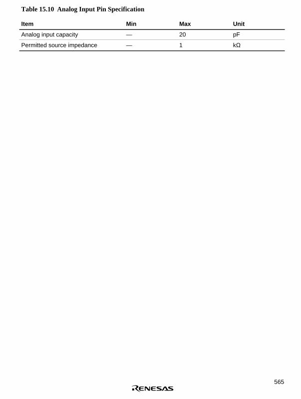
565
Table 15.10 Analog Input Pin Specification
Item Min Max Unit
Analog input capacity — 20 pF
Permitted source impedance — 1 kΩ

566

567
Section 16 Mid-Speed A/D Converter (A Mask)
16.1 Overview
The mid-speed A/D converter has 10 bit resolution, and can select from a maximum of eightchannels of analog input.
The mid-speed A/D converter is structured by two independent modules (A/D0 and A/D1)
16.1.1 Features
The mid-speed A/D converter has the following features:
• 10-bit resolution
• Eight input channels (four channels times two)
• Analog conversion voltage range setting is selectable
Using the standard voltage pin (AVref) as an analog standard voltage (Vref), conversion ofanalog input from 0V to Vref (only with SH7041A, SH7043A, and SH7045).
(Connected to AVCC internally in the SH7040A, SH7042A, and SH7044.)
• High speed conversion
Minimum conversion time: per channel
Operation frequency: f≤20MHz, CKS=0, 1
6.7µs (20MHz, CKS=1)
Operation frequency: f>20MHz, CKS=0
9.3µs (28.7MHz, CKS=0)
• Multiple conversion modes
Single mode/scan mode
2 channel simultaneous conversion
• Three types of conversion start
Software, timer conversion start trigger (MTU), or ADTRG pin can be selected.
• Eight data registers
Conversion results stored in 16-bit data registers corresponding to each channel.
• Sample and hold function
• A/D conversion end interrupt generation
An A/D conversion end interrupt (ADI) can be generated on completion of A/Dconversion.
• Furthermore, ADI0 (A/D0 interrupt request) can activate DTC and ADI1 (A/D1 interruptrequest) can activate DMAC.

568
16.1.2 Block Diagram
Figure 16.1 is the block diagram of the mid-speed A/D converter.
AVCC, AVref and AVSS pins of both A/D are common in LSI.
A/D0
+
−
+
−
AVcc
AVref
AVss
AN0
AN1
AN2
AN3
A/D1
AVcc
AVref
AVss
AN4
AN5
AN6
AN7
Interrupt signal ADI0 (DTC)
Interrupt signal ADI1 (DMAC)
Module data bus
Module data bus
(Only with 144 pin)
(Only with 144 pin)
10-bit D/A
Con
tinuo
us
com
paris
on
regi
ster
AD
DR
A0
AD
DR
B0
AD
DR
C0
AD
DR
D0
AD
CS
R0
AD
CR
0 Bus
inte
rfac
e
Ana
log
mul
tiple
xer
Con
tinuo
us
com
paris
on
regi
ster
AD
DR
A1
AD
DR
B1
AD
DR
C1
AD
DR
D1
AD
CS
R1
AD
CR
1
Bus
inte
rfac
e
10-bit D/A
Ana
log
mul
tiple
xer
Sample & hold circuit
Comparator Control circuit
Sample & hold circuit
Comparator Control circuit
Port trigger
MTU trigger
Logical sum
Figure 16.1 Mid-Speed A/D Converter Block Diagram

569
16.1.3 Pin Configuration
Table 16.1 shows the input pins used with the mid-speed A/D converter.
The AVCC and AVSS pins are for the mid-speed A/D converter internal analog section powersupply. AVref pin is the A/D conversion standard voltage.
Table 16.1 Pin Configuration
Pin Abbreviation I/O Function
Analog supply AvCC I Analog section power supply
Analog ground AVSS I Analog section ground and A/D conversionstandard voltage
Standard voltage AVref* I A/D conversion standard voltage(SH7041A, SH7043A, and SH7045 only)
A/D0 Analog input 0 AND I Analog input channel 0
Analog input 1 AN1 I Analog input channel 1
Analog input 2 AN2 I Analog input channel 2
Analog input 3 AN3 I Analog input channel 3
A/D1 Analog input 4 AN4 I Analog input channel 4
Analog input 5 AN5 I Analog input channel 5
Analog input 6 AN6 I Analog input channel 6
Analog input 7 AN7 I Analog input channel 7
A/D external trigger input ADTRG I External trigger for A/D conversion start
Note: * In the SH7040A, SH7042A, and SH7044, AVref is connected to AVCC internally.

570
16.1.4 Register Configuration
Table 16.2 shows the register configuration of the mid-speed A/D converter.
Table 16.2 Register Configuration
Name Abbreviation R/W Initial Value Address Access Size
A/D0 data register AH ADDRA0H R H'00 H'FFFF8400 8, 16
A/D0 data register AL ADDRA0L R H'00 H'FFFF8401 8
A/D0 data register BH ADDRB0H R H'00 H'FFFF8402 8, 16
A/D0 data register BL ADDRB0L R H'00 H'FFFF8403 8
A/D0 data register CH ADDRC0H R H'00 H'FFFF8404 8, 16
A/D0 data register CL ADDRC0L R H'00 H'FFFF8405 8
A/D0 data register DH ADDRD0H R H'00 H'FFFF8406 8, 16
A/D0 data register DL ADDRD0L R H'00 H'FFFF8407 8
A/D0 control/status register ADCSR0 R/(W)* H'00 H'FFFF8410 8, 16
A/D0 control register ADCR0 R/W H'7F H'FFFF8412 8, 16
A/D1 data register AH ADDRA1H R H'00 H'FFFF8408 8, 16
A/D1 data register AL ADDRA1L R H'00 H'FFFF8409 8
A/D1 data register BH ADDRB1H R H'00 H'FFFF840A 8, 16
A/D1 data register BL ADDRB1L R H'00 H'FFFF840B 8
A/D1 data register CH ADDRC1H R H'00 H'FFFF840C 8, 16
A/D1 data register CL ADDRC1L R H'00 H'FFFF840D 8
A/D1 data register DH ADDRD1H R H'00 H'FFFF840E 8, 16
A/D1 data register DL ADDRD1L R H'00 H'FFFF840F 8
A/D1 control/status register ADCSR1 R/(W)* H'00 H'FFFF8411 8
A/D1 control register ADCR1 R/W H'7F H'FFFF8413 8
Note: * Only 0 can be written to bit 7 to clear the flag.

571
16.2 Register Descriptions
16.2.1 A/D Data Register A–D (ADDRA0–ADDRD0, ADDRA1–ADDRD1)
A/D registers are special registers that read stored results of A/D conversion in 16 bits. There areeight registers: ADDRA0–ADDRD0 (A/D0) and ADDRA1–ADDRD1 (A/D1).
The A/D converted data is 10 bit data which is to the ADDR of the corresponding convertedchannel for storage. The upper 8 bits of the A/D converted data correspond to the upper byte of theADDR and the lower 2 bits correspond to the lower byte. Bits 5–0 of the lower byte of ADDR arereserved and always read 0. Analog input channels and correspondence to ADDR are shown intable 16.3.
ADDR can always be read from the CPU. The upper byte may be read directly. The lower byte istransferred through the temporary register (TEMP). For details, see section 16.3, Interface withCPU.
ADDR is initialized to H'0000 during power-on reset or standby mode. ADDR will not beinitialized by manual reset.
15 14 13 12 11 10 9 8 7 6 5 4 3 2 1 0
AD9 AD8 AD7 AD6 AD5 AD4 AD3 AD2 AD1 AD0 — — — — — —
0 0 0 0 0 0 0 0 0 0 0 0 0 0 0 0
R
ADDRn :
R/W : R R R R R R R R R R R R R R R(n=A to D)
Initial value :
Bit :
Table 16.3 Analog Input Channel and ADDRA–ADDRD Correspondence
Analog Input Channel A/D Data Register Module
AN0 ADDRA0 A/D0
AN1 ADDRB0
AN2 ADDRC0
AN3 ADDRD0
AN4 ADDRA1 A/D1
AN5 ADDRB1
AN6 ADDRC1
AN7 ADDRD1

572
16.2.2 A/D Control/Status Register (ADCSR0, ADCSR1)
The A/D control/status registers (ADCSR0, 1) are registers that can read/write in 8 bits and controlA/D converter operations such as mode selection. There are the ADCSR0 (A/D0) and ADCSR1(A/D1).
The ADCSR is initialized to H'00 during power-on reset or standby mode. Manual reset does notinitialize ADCSR.
ADIEADF ADST SCAN CKS — CH1 CH0
7 6 5 4 3 2 1 0
0 0 0 0 0 0 1 0
R/W : R/(W)* R/W R/W R/W R/W R R/W R/W
Bit :
Initial value :
Note: * Only 0 can be written to clear the flag.
• Bit 7—A/D End Flag (ADF): Status flag that indicates end of A/D conversion.
Bit 7:
ADF Description
0 [Clear conditions] (Initial value)
1. Writing 0 to ADF after reading ADF with ADF=1
2. When registers of the mid-speed converter are accessed after the DMAC and DTCare activated by ADI interrupt.
1 [Set conditions]
1. Single mode: When A/D conversion is complete
2. Scan mode: When A/D conversion of all designated channels are complete
• Bit 6—A/D Interrupt Enable (ADIE): Enables or disables interrupt request (ADI) due tocompletion of A/D conversion.
Bit 6:
ADIE Description
0 Disables interrupt request (ADI) due to completion of A/D conversion (Initial value)
1 Enables interrupt request (ADI) due to completion of A/D conversion

573
• Bit 5—A/D Start (ADST): Selects start/end of A/D conversion. A1 is maintained during A/Dconversion start. It is also possible to set a 1 by the A/D conversion trigger input pin(ADTRG).
Bit 5:
ADST Description
0 A/D conversion halted (Initial value)
1 1. Single mode: Starts A/D conversion. Automatically clears to 0 when conversion ofthe designated channel is complete
2. Scan mode: Starts A/D conversion. Continuous conversion until cleared to 0 by thesoftware
• Bit 4—Scan Mode (SCAN): Selects the A/D conversion mode from single mode and scanmode. For operations during single/scan mode, see section 16.4, Operation. When switchingmodes, proceed while ADST=0.
Bit 4:
SCAN Description
0 Single mode (Initial value)
1 Scan mode
• Bit 3—Clock Select (CKS): Sets the A/D conversion time. Proceed conversion time switchwhile adst=0. Always set CKS=0 when operating frequency exceeds 20MHz.
Bit 3:
CKS Description
0 Conversion time = 266 states (max) (Initial value)
1 Conversion time = 134 states (max)
• Bit 2—Reserved bit: Bit 2 always reads 0. Furthermore, always write 0.
• Bits 1, 0—Channel select 1, 0 (CH1, CH0): Selects the analog input channel along with theSCAN bit. Switch channels while ADST=0.

574
ChannelSelection Description
Single mode Scan mode
CH1 CH0 A/D0 A/D1 A/D0 A/D1
0 0 AN0(Initial value)
AN4(Initial value)
AN0 AN4
1 AN1 AN5 AN0, AN1 AN4, AN5
1 0 AN2 AN6 AN0, AN1 AN4–AN6
1 AN3 AN7 AN0–AN3 AN4–AN7
16.2.3 A/D Control Register (ADCR0, ADCR1)
A/D control registers (ADCR0, 1) are registers that can read/write in 8 bits and enables or disablesA/D conversion start of the external trigger input. There are the ADCR0 (A/D0) and ADCR1(A/D1).
ADCR is initialized to H'7F during power-on reset and standby mode. Manual reset does notinitialize ADCR.
—TRGE — — — — — —
7 6 5 4 3 2 1 0
0 1 1 1 1 1 1 1
R/W : R/W R R R R R R R
Initial value :
Bit :
• Bit 7—Trigger Enable (TRGE): Enables or disables A/D conversion start of input fromexternal or MTU trigger.
Bit 7:
TRGE Description
0 Disables A/D conversion start of external or MTU trigger (Initial value)
1 Starts A/D conversion on last transition edge of A/D conversion trigger input pin(ADTRG) or MTU trigger.
A/D0 and A/D1 are common for external trigger pin and MTU trigger.
A/D0 and A/D1 settings are of logical sum.
• Bits 6–0—Reserved bits: These bits always read as 1. The write value should always be 1.

575
16.3 Interface with CPU
Although A/D data register ADDR (ADDRA0–ADDRD0, ADDRA1–ADDRD1) are 16-bitregisters, the bus width within the chip that integrates with the CPU is 8-bits. So, upper and lowerdata of the ADDR must be read separately.
To avoid change in data while reading the upper/lower 2 bytes of ADDR, the lower byte data isread through the temporary register (TEMP). The upper byte data can be read directly.
The procedure for reading data from ADDR is as follows: First, read the upper byte data fromADDR. At this time, the upper byte data is read directly into the CPU and the lower byte data istransferred to TEMP of the mid-speed A/D converter. Next, read the lower byte to read the TEMPcontents into the CPU.
When reading the ADDR in byte size, read the upper byte before the lower byte. Furthermore, it ispossible to read only the upper byte, however, please note that contents are not guaranteed whenreading only the lower byte. In addition, when reading ADDR in word size, upper byte isautomatically read before the lower byte.
Figure 16.2 shows the data flow when reading from ADDR.
CPU(H'AA)
ADDRnH(H'AA)
ADDRnL(H'40)
TEMP(H'40)
CPU(H'40)
ADDRnH(H'AA)
ADDRnL(H'40)
TEMP(H'40)
<Reading the upper byte>
Bus interfaceModule data bus
Bus interfaceModule data bus
<Reading of the lower byte>
Figure 16.2 ADDR Access Operation (During Reading of (H'AA40))

576
16.4 Operation
The mid-speed converter operates using the continuous comparison method and is equipped with10-bit resolution. Operations for the single and scan modes are explained below.
16.4.1 Single Mode (SCAN=0)
The single mode is selected when executing A/D conversion for one channel only. A/D conversionis initiated when the ADST bit of the A/D control/status register is set to 1 by the software orexternal trigger input. The ADST bit is held to 1 during the A/D conversion and is automaticallycleared to 0 upon completion.
When conversion is complete, the ADF bit of ADCSR is set to 1. At this time, if the ADIE bit ofADCSR is 1, ADI interrupt request occurs.
The ADF bit can be cleared by writing 0 after reading ADF=1.
To switch modes or analog input channels during A/D conversion, clear the ADST bit to 0 andstop A/D conversion to avoid malfunction. After switching (mode/channel change and ADST bitsetting can be made at the same time), set the ADST bit to 1 to restart A/D conversion.
An example of operation when channel 1 (AN1) is selected in the single mode is shown in figure16.3 (the bit specification in the example is the ADCSR0 register).
1. Set operation mode to single mode (SCAN=0), input channel to AN1 (CH1=0, CH0=1) andA/D interrupt request to enable (ADIE) then start A/D conversion (ADST=1).
2. When A/D conversion is complete, A/D conversion result is transferred to ADDRB0. At thesame time, ADF=1 will become ADF=0 and the mid-speed converter will standby forconversion.
3. Since ADF=1 and ADIE=1, ADI interrupt request will occur.
4. The A/D interrupt process routine will start.
5. After reading ADF=1, write 0 to ADF.
6. Read the A/D conversion result (ADDRB0) and process.
7. End A/D interrupt process routine execution. When ADST bit is set to 1, A/D conversionstarts, following steps (2) to (7) above.
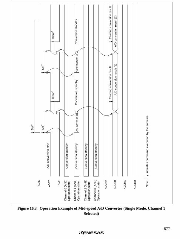
577
AD
IE
AD
ST
AD
F
AD
DR
A
AD
DR
B
AD
DR
C
AD
DR
D
Not
e: *
i
ndic
ates
com
man
d ex
ecut
ion
by th
e so
ftwar
e
Set
*
Set
* S
et*
Cle
ar*
A/D
con
vers
ion
star
t
Cle
ar*
Cha
nnel
3 (
AN
3)O
pera
tion
stat
e
Cha
nnel
0 (
AN
0)O
pera
tion
stat
e
Cha
nnel
1 (
AN
1)O
pera
tion
stat
e
Cha
nnel
2 (
AN
2)O
pera
tion
stat
e
Con
vers
ion
stan
dby
Con
vers
ion
stan
dby
Con
vers
ion
stan
dby
Con
vers
ion
stan
dby
Con
vers
ion
stan
dby
Con
vers
ion
stan
dby
A/D
con
vers
ion
(1)
A/D
con
vers
ion
(2)
Rea
ding
con
vers
ion
resu
ltR
eadi
ng c
onve
rsio
n re
sult
A/D
con
vers
ion
resu
lt (1
)A
/D c
onve
rsio
n re
sult
(2)
Figure 16.3 Operation Example of Mid-speed A/D Converter (Single Mode, Channel 1Selected)

578
16.4.2 Scan Mode (SCAN=1)
The scan mode is optimal for monitoring analog input of multiple channels (including channel 1).A/D conversion is started from channel 1 (AN0 for A/D0 and AN4 for A/D1) of the group whenthe ADST bit of the A/D control/status register (ADCSR) is set to 1 by the software or externaltrigger input.
When multiple channels are selected, A/D conversion of channel 2 (AN1 or AN5) is initiatedimmediately after completion of the channel 1 conversion.
To switch modes or analog input channels during A/D conversion, clear the ADST bit to 0 andstop A/D conversion to avoid malfunction. After switching (mode/channel change and ADST bitsetting can be made at the same time), set ADST bit to 1 to restart A/D conversion from channel 1.
An example of operation when three channels of A/D0 (AN0–2) are selected for A/D conversionis shown in figure 16.4 (the bit specification in the example is the ADCSR0 register).
1. Set operation mode to scan mode (SCAN=1), set analog channels to AN0–2 (CH1=1, CH0=0)then start A/D conversion (ADST=1).
2. When A/D conversion for channel 1 is complete, A/D conversion result is transferred toADDRA0.
Next, channel 2 (AN1) will automatically be selected and conversion will begin.
3. In the same manner, channel 3 will be converted (AN2).
4. When conversion of all of the selected channels (AN0–AN2) are complete, ADF will become1 and channel 1 (AN0) will again be selected and conversion will begin.
At this time, if the ADIE bit is set to 1, ADI interrupt request will occur after completing A/Dconversion.
5. Steps (2) to (4) will be repeated while ADST bit is set to 1.
A/D conversion will stop when setting the ADST bit to 0. When setting the ADST bit to 1,A/D conversion will start again from channel 1 (AN0).

579
AD
ST
AD
F
AD
DR
A
AD
DR
B
AD
DR
C
AD
DR
D
*2
A/D
con
tinuo
us c
onve
rsio
n
Set
*1
Cle
ar*1
Cle
ar*1
Cha
nnel
0 (
AN
0)O
pera
tion
cond
ition
Cha
nnel
1 (
AN
1)O
pera
tion
cond
ition
Cha
nnel
2 (
AN
2)O
pera
tion
cond
ition
Cha
nnel
3 (
AN
3)O
pera
tion
cond
ition
Con
vers
ion
stan
dby
Con
vers
ion
stan
dby
Con
vers
ion
stan
dby
Con
vers
ion
stan
dby
Con
vers
ion
stan
dby
Con
vers
ion
stan
dby
Con
vers
ion
stan
dby
Con
vers
ion
stan
dby
A/D
con
vers
ion(
1)
A/D
con
vers
ion(
2)
A/D
con
vers
ion(
3)
A/D
con
vers
ion(
4)
A/D
con
vers
ion(
5)
A/D
con
vers
ion
time
Tra
nsfe
r
A/D
con
vers
ion
resu
lt(1)
A/D
con
vers
ion
resu
lt(4)
A/D
con
vers
ion
resu
lt(2)
A/D
con
vers
ion
resu
lt(3)
Not
es:
*1
ind
icat
es c
omm
and
exec
utio
n by
the
softw
are
*
2 D
ata
is ig
nore
d du
ring
conv
ersi
on
Figure 16.4 Operation Example of Mid-speed A/D Converter (Scan Mode, Three ChannelsSelected) (AN0–AN2)

580
16.4.3 Input Sampling and A/D Conversion Time
The mid-speed A/D converter is equipped with a sample and hold circuit. The mid-speed A/Dconverter samples input after tD hours has elapsed since setting the ADST bit of the A/Dcontrol/status register (ADCSR) to 1, then begins conversion. The A/D conversion timing isshown in table 16.4.
The A/D conversion time, as shown in figure 16.5, includes both tD and input sampling time. Here,tD is determined by the write timing to ADCSR and is not constant. Thus the conversion timechanges in the range shown in table 16.4.
The conversion time shown in table 16.4 is the time for the first conversion. For the secondconversion and after, the time will be 256 state (fixed) for CKS=0 and 128 state (fixed) forCKS=1.
(1)
(2)
CK
ADF
t D t SPL
t CONV
< Key>(1): Write cycle of ADCSR(2): Address of ADCSR
Address
Write signal
Input sampling timing
tD: A/D conversion start delay timetSPL: Input sampling timetCONV: A/D conversion time
Figure 16.5 A/D Conversion Timing
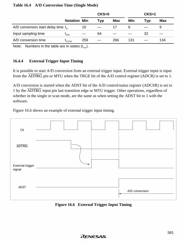
581
Table 16.4 A/D Conversion Time (Single Mode)
CKS=0 CKS=1
Notation Min Typ Max Min Typ Max
A/D conversion start delay time tD 10 — 17 6 — 9
Input sampling time tSPL — 64 — — 32 —
A/D conversion time tCCNV 259 — 266 131 — 134
Note: Numbers in the table are in states (tcyc).
16.4.4 External Trigger Input Timing
It is possible to start A/D conversion from an external trigger input. External trigger input is inputfrom the ADTRG pin or MTU when the TRGE bit of the A/D control register (ADCR) is set to 1.
A/D conversion is started when the ADST bit of the A/D control/status register (ADCSR) is set to1 by the ADTRG input pin last transition edge or MTU trigger. Other operations, regardless ofwhether in the single or scan mode, are the same as when setting the ADST bit to 1 with thesoftware.
Figure 16.6 shows an example of external trigger input timing.
ADTRG
External triggersignal
A/D conversion
CK
ADST
Figure 16.6 External Trigger Input Timing
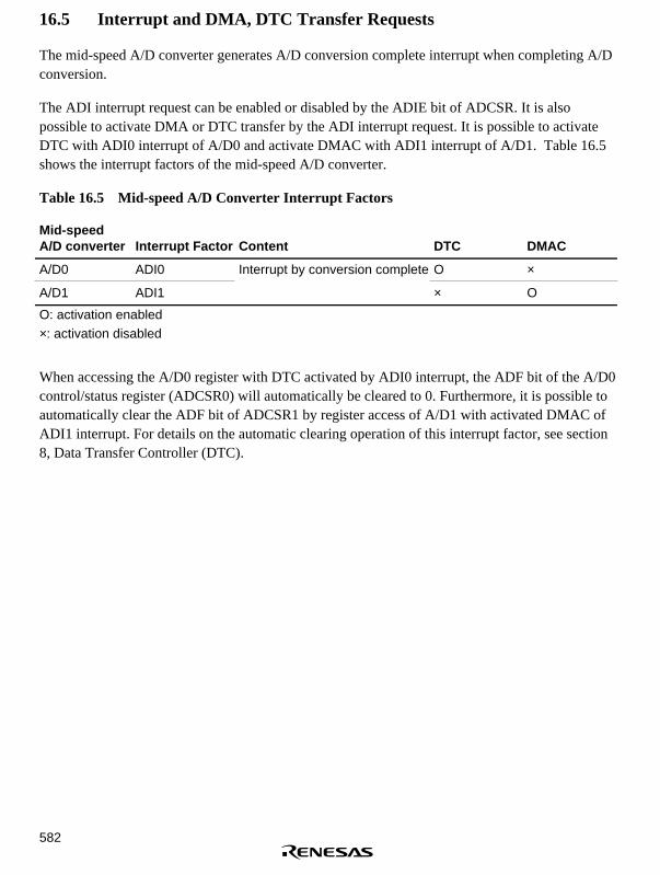
582
16.5 Interrupt and DMA, DTC Transfer Requests
The mid-speed A/D converter generates A/D conversion complete interrupt when completing A/Dconversion.
The ADI interrupt request can be enabled or disabled by the ADIE bit of ADCSR. It is alsopossible to activate DMA or DTC transfer by the ADI interrupt request. It is possible to activateDTC with ADI0 interrupt of A/D0 and activate DMAC with ADI1 interrupt of A/D1. Table 16.5shows the interrupt factors of the mid-speed A/D converter.
Table 16.5 Mid-speed A/D Converter Interrupt Factors
Mid-speedA/D converter Interrupt Factor Content DTC DMAC
A/D0 ADI0 Interrupt by conversion complete O ×
A/D1 ADI1 × O
O: activation enabled×: activation disabled
When accessing the A/D0 register with DTC activated by ADI0 interrupt, the ADF bit of the A/D0control/status register (ADCSR0) will automatically be cleared to 0. Furthermore, it is possible toautomatically clear the ADF bit of ADCSR1 by register access of A/D1 with activated DMAC ofADI1 interrupt. For details on the automatic clearing operation of this interrupt factor, see section8, Data Transfer Controller (DTC).

583
16.6 A/D Conversion Precision Definitions
The medium-speed A/D converter converts analog values input from analog input channels to 10-bit digital values by comparing them with an analog reference voltage. In this operation, theabsolute precision of the A/D conversion (i.e. the deviation between the input analog value and theoutput digital value) includes the following kinds of error.
(1) Offset error
(2) Full-scale error
(3) Quantization error
(4) Nonlinearity error
The above four kinds of error are described below with reference to figure 16.7. For the sake ofclarity, this figure shows 3-bit medium-speed A/D conversion rather than 10-bit medium-speedA/D conversion. Offset error (see figure 16.7 (1)) is the deviation between the actual A/Dconversion characteristic and the ideal A/D conversion characteristic when the digital output valuechanges from the minimum value (zero voltage) of 0000000000 (000 in the figure) to 0000000001(001 in the figure ). Full-scale error (see figure 16.7 (2)) is the deviation between the actual A/Dconversion characteristic and the ideal A/D conversion characteristic when the digital output valuechanges from 1111111110 (110 in the figure) to the maximum value (full-scale voltage) of111111111 (111 in the figure). Quantization error is the deviation inherent in the medium-speedA/D converter, given by 1/2 LSB (see figure 16.7 (3)). Nonlinearity error is the deviation betweenthe actual A/D conversion characteristic and the ideal A/D conversion characteristic from zerovoltage to full-scale voltage (see figure 16.7 (4)). This does not include offset error, full-scaleerror, and quantization error.
0 1/8 2/8 3/8 4/8 5/8 6/8 7/8 FS
111
110
101
100
011
010
001
000
Analog input voltage
(3) Quantization error
(4) Nonlinearity error
(2) Full-scale error
Ideal A/D conversion Characteristic
Ideal A/D conversion Characteristic
Digital output Digital output
FS : Full-scale voltage
FSAnalog input
voltage
Actual A/D conversion characteristic
(1) Offset error
Figure 16.7 A/D Conversion Precision Definitions
584
16.7 Usage Notes
The following points should be noted when using the mid-speed A/D converter.
16.7.1 Analog Voltage Settings
(1) Analog input voltage range
The voltage applied to analog input pins during A/D conversion should be in the range AVSS≤ ANn ≤ AVref (n = 0 to 7).
(2) AVCC and AVSS input voltages
For the AVCC and AVSS input voltages, set AVCC = VCC ±10% and AVSS = VSS. When themedium-speed A/D converter is not used, set AVCC = VCC and AVSS = VSS.
(3) AVref input voltage
For the AVref pin input voltage analog reference, set AVref ≤ AVCC. When the medium-speedA/D converter is not used, set AVref = AVCC.
(4) AVCC and AVref must be connected to the power supply (VCC) even if the medium-speed A/Dconverter is not used or is in standby mode.
16.7.2 Handling of Analog Input Pins
To prevent damage from surges and other abnormal voltages at the analog input pins (AN0-AN7),connect a protection circuit such as that shown in figure 16.8. This circuit also includes a CR filterfunction that suppresses error due to noise. The circuit shown here is only a design example;circuit constants must be decided on the basis of the actual operating conditions.
Figure 16.9 shows an equivalent circuit for the analog input pins, and table 16.6 summarizes theanalog input pin specifications.
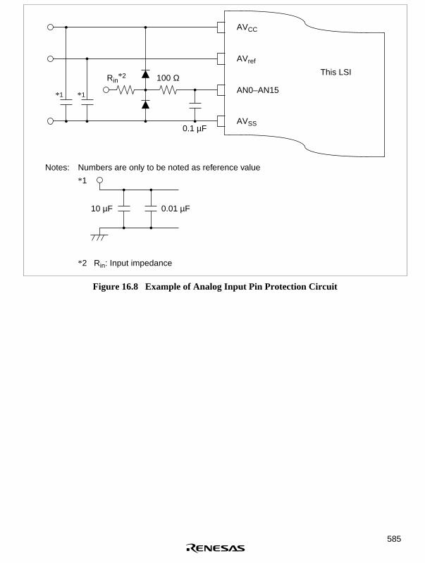
585
AVCC
AVref
AN0–AN15
AVSS
This LSI
Notes: Numbers are only to be noted as reference value
*1
*2 Rin: Input impedance
10 µF 0.01 µF
Rin*2
0.1 µF
100 Ω
*1*1
Figure 16.8 Example of Analog Input Pin Protection Circuit

586
AN0 to AN7
1.0kΩ
20pFΩ 1MΩ
Analog multiplexer Mid-speed A/D converter
Note : Numbers are only to be noted as reference value
Figure 16.9 Equivalent Circuit for the Analog Input Pins
Table 16.6 Analog Pin Specifications
Item Min Max Unit
Analog input capacitance — 20 pF
Permissible signal source impedance — 1 kΩ

587
Section 17 Compare Match Timer (CMT)
17.1 Overview
The SH7040 series has an on-chip compare match timer (CMT) configured of 16-bit timers fortwo channels. The CMT has 16-bit counters and can generate interrupts at set intervals.
17.1.1 Features
The CMT has the following features:
• Four types of counter input clock can be selected
One of four internal clocks (φ/8, φ/32, φ/128, φ/512) can be selected independently for eachchannel.
• Interrupt sources
A compare match interrupt can be requested independently for each channel.
17.1.2 Block Diagram
Figure 17.1 shows a block diagram of the CMT.

588
CM10
Control circuit
Internal bus
Clock selection Control circuit Clock selection
CMI1φ/8 φ/32 φ/128 φ/512 φ/8 φ/32 φ/128 φ/512
CM
CS
R1
CM
CO
R1
CM
CN
T1
CM
CN
T0
CM
CO
R0
Com
para
tor
CM
ST
R
CM
CS
R0
Com
para
tor
BusinterfaceModule bus
CMT
CMSTR:CMCSR:CMCOR:CMCNT:
CMI:
Compare match timer start registerCompare match timer control/status registerCompare match timer constant registerCompare match timer counterCompare match interrupt
Figure 17.1 CMT Block Diagram

589
17.1.3 Register Configuration
Table 17.1 summarizes the CMT register configuration.
Table 17.1 Register Configuration
Channel Name Abbreviation R/WInitialValue Address
Access Size(Bits)
Shared Compare match timerstart register
CMSTR R/W H'0000 H'FFFF83D0 8, 16, 32
0 Compare match timercontrol/status register 0
CMCSR0 R/(W)* H'0000 H'FFFF83D2 8, 16, 32
Compare match timercounter 0
CMCNT0 R/W H'0000 H'FFFF83D4 8, 16, 32
Compare match timerconstant register 0
CMCOR0 R/W H'FFFF H'FFFF83D6 8, 16, 32
1 Compare match timercontrol/status register 1
CMCSR1 R/(W)* H'0000 H'FFFF83D8 8, 16, 32
Compare match timercounter 1
CMCNT1 R/W H'0000 H'FFFF83DA 8, 16, 32
Compare match timerconstant register 1
CMCOR1 R/W H'FFFF H'FFFF83DC 8, 16, 32
Note: * The only value that can be written to the CMCSR0 and CMCSR1 CMF bits is a 0 to clearthe flags.

590
17.2 Register Descriptions
17.2.1 Compare Match Timer Start Register (CMSTR)
The compare match timer start register (CMSTR) is a 16-bit register that selects whether tooperate or halt the channel 0 and channel 1 counters (CMCNT). It is initialized to H'0000 bypower-on resets and by standby mode. Manual reset does not initialize CMSTR.
Bit: 15 14 13 12 11 10 9 8
— — — — — — — —
Initial value: 0 0 0 0 0 0 0 0
R/W: R R R R R R R R
Bit: 7 6 5 4 3 2 1 0
— — — — — — STR1 STR0
Initial value: 0 0 0 0 0 0 0 0
R/W: R R R R R R R/W R/W
• Bits 15–2—Reserved: These bits always read as 0. The write value should always be 0.
• Bit 1—Count Start 1 (STR1): Selects whether to operate or halt compare match timer counter1.
Bit 1: STR1 Description
0 CMCNT1 count operation halted (initial value)
1 CMCNT1 count operation
• Bit 0—Count Start 0 (STR0): Selects whether to operate or halt compare match timer counter0.
Bit 0: STR0 Description
0 CMCNT0 count operation halted (initial value)
1 CMCNT0 count operation

591
17.2.2 Compare Match Timer Control/Status Register (CMCSR)
The compare match timer control/status register (CMCSR) is a 16-bit register that indicates theoccurrence of compare matches, sets the enable/disable of interrupts, and establishes the clockused for incrementation. It is initialized to H'0000 by power-on resets and by standby mode.Manual reset does not initialize CMCSR.
Bit: 15 14 13 12 11 10 9 8
— — — — — — — —
Initial value: 0 0 0 0 0 0 0 0
R/W: R R R R R R R R
Bit: 7 6 5 4 3 2 1 0
CMF CMIE — — — — CKS1 CKS0
Initial value: 0 0 0 0 0 0 0 0
R/W: R/(W)* R/W R R R R R/W R/W
Note: * The only value that can be written is a 0 to clear the flag.
• Bits 15–8 and 5–2—Reserved: These bits always read as 0. The write value should always be0.
• Bit 7—Compare Match Flag (CMF): This flag indicates whether or not the CMCNT andCMCOR values have matched.
Bit 7: CMF Description
0 CMCNT and CMCOR values have not matched (initial status)
Clear condition: Write a 0 to CMF after reading a 1 from it
1 CMCNT and CMCOR values have matched
• Bit 6—Compare Match Interrupt Enable (CMIE): Selects whether to enable or disable acompare match interrupt (CMI) when the CMCNT and CMCOR values have matched (CMF =1).
Bit 6: CMIE Description
0 Compare match interrupts (CMI) disabled (initial status)
1 Compare match interrupts (CMI) enabled

592
• Bits 1, 0—Clock Select 1, 0 (CKS1, CKS0): These bits select the clock input to the CMCNTfrom among the four internal clocks obtained by dividing the system clock (φ). When the STRbit of the CMSTR is set to 1, the CMCNT begins incrementing with the clock selected byCKS1 and CKS0.
Bit 1: CKS1 Bit 0: CKS0 Description
0 0 φ/8 (initial status)
1 φ/32
1 0 φ/128
1 φ/512
17.2.3 Compare Match Timer Counter (CMCNT)
The compare match timer counter (CMCNT) is a 16-bit register used as an upcounter forgenerating interrupt requests.
When an internal clock is selected with the CKS1, CKS0 bits of the CMCSR register and the STRbit of the CMSTR is set to 1, the CMCNT begins incrementing with that clock. When the CMCNTvalue matches that of the compare match timer constant register (CMCOR), the CMCNT iscleared to H'0000 and the CMF flag of the CMCSR is set to 1. If the CMIE bit of the CMCSR isset to 1 at this time, a compare match interrupt (CMI) is requested.
The CMCNT is initialized to H'0000 by power-on resets and by standby mode. Manual reset doesnot initialize CMCNT.
Bit: 15 14 13 12 11 10 9 8
Initial value: 0 0 0 0 0 0 0 0
R/W: R/W R/W R/W R/W R/W R/W R/W R/W
Bit: 7 6 5 4 3 2 1 0
Initial value: 0 0 0 0 0 0 0 0
R/W: R/W R/W R/W R/W R/W R/W R/W R/W

593
17.2.4 Compare Match Timer Constant Register (CMCOR)
The compare match timer constant register (CMCOR) is a 16-bit register that sets the comparematch period with the CMCNT.
The CMCOR is initialized to H'FFFF by power-on resets and by standby mode. There is noinitializing with manual reset.
Bit: 15 14 13 12 11 10 9 8
Initial value: 1 1 1 1 1 1 1 1
R/W: R/W R/W R/W R/W R/W R/W R/W R/W
Bit: 7 6 5 4 3 2 1 0
Initial value: 1 1 1 1 1 1 1 1
R/W: R/W R/W R/W R/W R/W R/W R/W R/W
17.3 Operation
17.3.1 Period Count Operation
When an internal clock is selected with the CKS1, CKS0 bits of the CMCSR register and the STRbit of the CMSTR is set to 1, the CMCNT begins incrementing with the selected clock. When theCMCNT counter value matches that of the compare match constant register (CMCOR), theCMCNT counter is cleared to H'0000 and the CMF flag of the CMCSR register is set to 1. If theCMIE bit of the CMCSR register is set to 1 at this time, a compare match interrupt (CMI) isrequested. The CMCNT counter begins counting up again from H'0000.
Figure 17.2 shows the compare match counter operation.
CMCOR
H'0000
CMCNT value
Time
Counter cleared byCMCOR compare match
Figure 17.2 Counter Operation

594
17.3.2 CMCNT Count Timing
One of four clocks (φ/8, φ/32, φ/128, φ/512) obtained by dividing the system clock (CK) can beselected by the CKS1, CKS0 bits of the CMCSR. Figure 17.3 shows the timing.
CK
N – 1 N N + 1
Internal clock
CMCNT inputclock
CMCNT
Figure 17.3 Count Timing
17.4 Interrupts
17.4.1 Interrupt Sources and DTC Activation
The CMT has a compare match interrupt for each channel, with independent vector addressesallocated to each of them. The corresponding interrupt request is output when the interrupt requestflag CMF is set to 1 and the interrupt enable bit CMIE has also been set to 1.
When activating CPU interrupts by interrupt request, the priority between the channels can bechanged by using the interrupt controller settings. See section 6, Interrupt Controller (INTC), fordetails.
Interrupt requests can also be used as data transfer controller (DTC) activating sources. In thiscase, channel priorities are fixed. See section 8, Data Transfer Controller (DTC), for details.
17.4.2 Compare Match Flag Set Timing
The CMF bit of the CMCSR register is set to 1 by the compare match signal generated when theCMCOR register and the CMCNT counter match. The compare match signal is generated uponthe final state of the match (timing at which the CMCNT counter matching count value isupdated). Consequently, after the CMCOR register and the CMCNT counter match, a comparematch signal will not be generated until a CMCNT counter input clock occurs. Figure 17.4 showsthe CMF bit set timing.
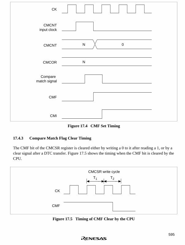
595
CK
CMCNTinput clock
CMCNT
CMCOR
Compare match signal
CMF
CMI
N
N
0
Figure 17.4 CMF Set Timing
17.4.3 Compare Match Flag Clear Timing
The CMF bit of the CMCSR register is cleared either by writing a 0 to it after reading a 1, or by aclear signal after a DTC transfer. Figure 17.5 shows the timing when the CMF bit is cleared by theCPU.
T2T1
CK
CMF
CMCSR write cycle
Figure 17.5 Timing of CMF Clear by the CPU
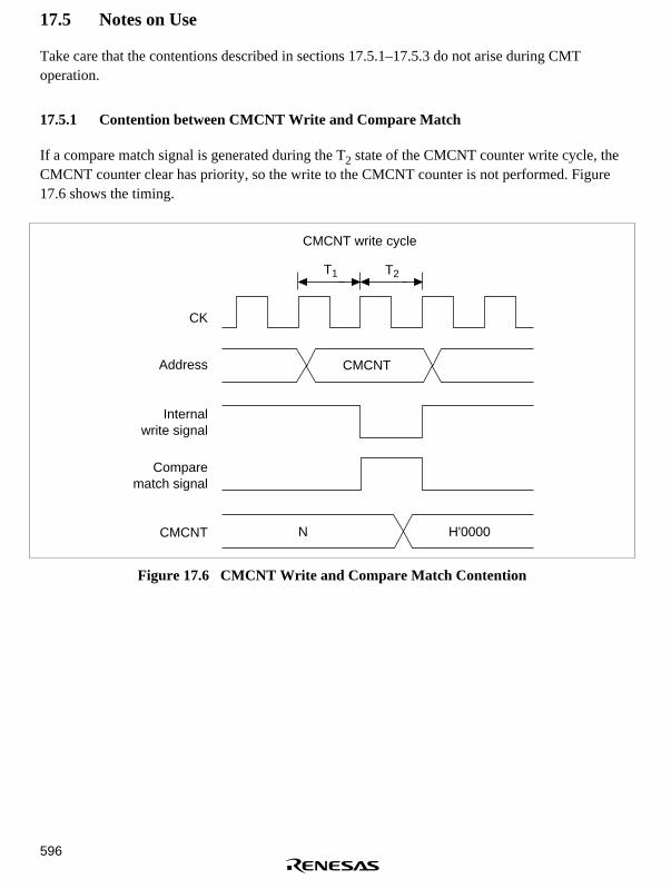
596
17.5 Notes on Use
Take care that the contentions described in sections 17.5.1–17.5.3 do not arise during CMToperation.
17.5.1 Contention between CMCNT Write and Compare Match
If a compare match signal is generated during the T2 state of the CMCNT counter write cycle, theCMCNT counter clear has priority, so the write to the CMCNT counter is not performed. Figure17.6 shows the timing.
T1 T2
CK
Address
Internalwrite signal
Comparematch signal
CMCNT
CMCNT write cycle
CMCNT
N H'0000
Figure 17.6 CMCNT Write and Compare Match Contention

597
17.5.2 Contention between CMCNT Word Write and Incrementation
If an increment occurs during the T2 state of the CMCNT counter word write cycle, the counterwrite has priority, so no increment occurs. Figure 17.7 shows the timing.
CMCNT write data
T1 T2
CK
Address
Internalwrite signal
Comparematch signal
CMCNT
CMCNT write cycle
CMCNT
N M
Figure 17.7 CMCNT Word Write and Increment Contention

598
17.5.3 Contention between CMCNT Byte Write and Incrementation
If an increment occurs during the T2 state of the CMCNT byte write cycle, the counter write haspriority, so no increment of the write data results on the writing side. The byte data on the side notperforming the writing is also not incremented, so the contents are those before the write.
Figure 17.8 shows the timing when an increment occurs during the T2 state of the CMCNTH writecycle.
T1 T2
CK
Address
Internalwrite signal
CMCNTinput clock
CMCNTH
CMCNT write cycle
CMCNTH
N M
CMCNTH write data
X XCMCNTL
Figure 17.8 CMCNT Byte Write and Increment Contention

599
Section 18 Pin Function Controller
18.1 Overview
The pin function controller (PFC) is composed of registers for selecting the function ofmultiplexed pins and the direction of input/output. Table 18.1 lists the SH7040 Series’smultiplexed pins. The multiplex pin functions have restrictions dependent on the operating mode.Table 18.2 lists the pin functions and initial values for each operating mode.
Table 18.1 Multiplexed Pins
PortFunction 1(Related Module)
Function 2(Related Module)
Function 3(Related Module)
Function 4(Related Module)
FP-112
FP-144
TFP-120
A PA23 I/O (port) WRHH output (BSC) — — — 1 —
PA22 I/O (port) WRHL output (BSC) — — — 3 —
PA21 I/O (port) CASHH output (BSC) — — — 4 —
PA20 I/O (port) CASHL output (BSC) — — — 29 —
PA19 I/O (port) BACK output (BSC) DRAK1 output(DMAC)
— — 30 —
PA18 I/O (port) BREQ input (BSC) DRAK0 output(DMAC)
— — 33 —
PA17 /O (port) WAIT input (BSC) — — — 101 —
PA16 I/O (port) AH output (BSC) — — — 100 —
PA15 I/O (port) CK output (CPG) — — 83 107 88
PA14 I/O (port) RD output (BSC) — — 34 43 37
PA13 I/O (port) WRH output (BSC) — — 36 47 39
PA12 I/O (port) WRL output (BSC) — — 38 48 41
PA11 I/O (port) CS1 output (BSC) — — 40 49 43
PA10 I/O (port) CS0 output (BSC) — — 41 50 44
PA9 I/O (port) TCLKD input (MTU) IRQ3 (INTC) — 42 51 45
PA8 I/O (port) TCLKC input (MTU) IRQ2 (INTC) — 43 52 46
PA7 I/O (port) TCLKB input (MTU) CS3 output (BSC) — 44 53 47
PA6 I/O (port) TCLKA input (MTU) CS2 output (BSC) — 45 54 48
PA5 I/O (port) SCK1 I/O (SCI) DREQ1 input(DMAC)
IRQ1 input (INTC) 46 136 49

600
Table 18.1 Multiplexed Pins (cont)
PortFunction 1(Re-lated Module)
Function 2(Related Module)
Function 3(Related Module)
Function 4(Related Module)
FP-112
FP-144
TFP-120
A PA4 I/O (port) TxD1 output (SCI) — — 47 134 50
PA3 I/O (port) RxD1 input (SCI) — — 48 133 51
PA2 I/O (port) SCK0 I/O (SCI) DREQ0 input(DMAC)
IRQ0 input(INTC)
49 132 52
PA1 I/O (port) TxD0 output (SCI) — — 50 131 53
PA0 I/O (port) RxD0 input (SCI) — — 51 130 54
B PB9 I/O (port) IRQ7 input (INTC) A21 output (BSC) ADTRG input (A/D) 32 41 35
PB8 I/O (port) IRQ6 input (INTC) A20 output (BSC) WAIT input (BSC) 31 39 34
PB7 I/O (port) IRQ5 input (INTC) A19 output (BSC) BREQ input (BSC) 30 38 33
PB6 I/O (port) IRQ4 input (INTC) A18 output (BSC) BACK output (BSC) 29 37 32
PB5 I/O (port) IRQ3 input (INTC) POE3 input (port) RDWR output (BSC)28 36 29
PB4 I/O (port) IRQ2 input (INTC) POE2 input (port) CASH output (BSC) 26 34 27
PB3 I/O (port) IRQ1 input (INTC) POE1 input (port) CASL output (BSC) 25 32 26
PB2 I/O (port) IRQ0 input (INTC) POE0 input (port) RAS output (BSC) 24 31 25
PB1 I/O (port) A17 input (BSC) — — 22 27 23
PB0 I/O (port) A16 output (BSC) — — 20 25 21
C PC15 I/O (port) A15 output (BSC) — — 19 24 20
PC14 I/O (port) A14 output (BSC) — — 18 23 19
PC13 I/O (port) A13 output (BSC) — — 17 22 18
PC12 I/O (port) A12 output (BSC) — — 16 21 17
PC11 I/O (port) A11 output (BSC) — — 15 20 16
PC10 I/O (port) A10 output (BSC) — — 14 19 15
PC9 I/O (port) A9 output (BSC) — — 13 18 14
PC8 I/O (port) A8 output (BSC) — — 12 17 13
PC7 I/O (port) A7 output (BSC) — — 11 16 12

601
Table 18.1 Multiplexed Pins (cont)
PortFunction 1(Related Module)
Function 2(Related Module)
Function 3(Related Module)
Function 4(Related Module)
FP-112
FP-144
TFP-120
C PC6 I/O (port) A6 output (BSC) — — 10 15 11
PC5 I/O (port) A5 output (BSC) — — 9 13 10
PC4 I/O (port) A4 output (BSC) — — 8 11 9
PC3 I/O (port) A3 output (BSC) — — 7 10 8
PC2 I/O (port) A2 output (BSC) — — 6 9 7
PC1 I/O (port) A1 output (BSC) — — 5 8 6
PC0 I/O (port) A0 output (BSC) — — 4 7 5
D PD31 I/O (port) D31 I/O (BSC) ADTRG input (A/D) — — 45 —
PD30 I/O (port) D30 I/O (BSC) IRQOUT output(INTC)
— — 46 —
PD29 I/O (port) D29 I/O (BSC) CS3 output (BSC) — — 56 —
PD28 I/O (port) D28 I/O (BSC) CS2 output (BSC) — — 57 —
PD27 I/O (port) D27 I/O (BSC) DACK1 output(DMAC)
— — 58 —
PD26 I/O (port) D26 I/O (BSC) DACK0 output(DMAC)
— — 59 —
PD25 I/O (port) D25 I/O (BSC) DREQ1 input(DMAC)
— — 60 —
PD24 I/O (port) D24 I/O (BSC) DREQ0 input(DMAC)
— — 62 —
PD23 I/O (port) D23 I/O (BSC) IRQ7 input (INTC) — — 64 —
PD22 I/O (port) D22 I/O (BSC) IRQ6 input (INTC) — — 65 —
PD21 I/O (port) D21 I/O (BSC) IRQ5 input (INTC) — — 66 —
PD20 I/O (port) D20 I/O (BSC) IRQ4 input (INTC) — — 67 —
PD19 I/O (port) D19 I/O (BSC) IRQ3 input (INTC) — — 68 —
PD18 I/O (port) D18 I/O (BSC) IRQ2 input (INTC) — — 69 —
PD17 I/O (port) D17 I/O (BSC) IRQ1 input (INTC) — — 70 —
PD16 I/O (port) D16 I/O (BSC) IRQ0 input (INTC) — — 72 —
PD15 I/O (port) D15 I/O (BSC) — — 52 73 55
PD14 I/O (port) D14 I/O (BSC) — — 53 74 56

602
Table 18.1 Multiplexed Pins (cont)
PortFunction 1(Related Module)
Function 2(Related Module)
Function 3(Related Module)
Function 4(Related Module)
FP-112
FP-144
TFP-120
D PD13 I/O (port) D13 I/O (BSC) — — 54 75 57
PD12 I/O (port) D12 I/O (BSC) — — 56 76 59
PD11 I/O (port) D11 I/O (BSC) — — 57 78 62
PD10 I/O (port) D10 I/O (BSC) — — 58 80 63
PD9 I/O (port) D9 I/O (BSC) — — 59 81 64
PD8 I/O (port) D8 I/O (BSC) — — 60 82 65
PD7 I/O (port) D7 I/O (BSC) — — 62 83 67
PD6 I/O (port) D6 I/O (BSC) — — 63 84 68
PD5 I/O (port) D5 I/O (BSC) — — 64 86 69
PD4 I/O (port) D4 I/O (BSC) — — 66 88 71
PD3 I/O (port) D3 I/O (BSC) — — 67 89 72
PD2 I/O (port) D2 I/O (BSC) — — 68 90 73
PD1 I/O (port) D1 I/O (BSC) — — 69 91 74
PD0 I/O (port) D0 I/O (BSC) — — 70 92 75
E PE15 I/O (port) TIOC4D I/O (MTU) DACK1 output(DMAC)
IRQOUT output(INTC)
2 5 3
PE14 I/O (port) TIOC4C I/O (MTU) DACK0 output(DMAC)
AH output (BSC) 1 2 2
PE13 I/O (port) TIOC4B I/O (MTU) MRES input (INTC) — 112 144 120
PE12 I/O (port) TIOC4A I/O (MTU) — — 111 143 119
PE11 I/O (port) TIOC3D I/O (MTU) — — 110 142 118
PE10 I/O (port) TIOC3C I/O (MTU) — — 108 140 116
PE9 I/O (port) TIOC3B I/O (MTU) — — 107 139 115
PE8 I/O (port) TIOC3A I/O (MTU) — — 106 138 114
PE7 I/O (port) TIOC2B I/O (MTU) — — 105 137 113
PE6 I/O (port) TIOC2A I/O (MTU) — — 104 116 112
PE5 I/O (port) TIOC1B I/O (MTU) — — 102 115 109
PE4 I/O (port) TIOC1A I/O (MTU) — — 89 114 96
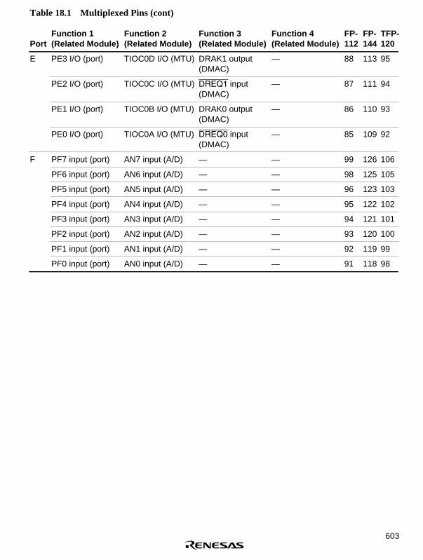
603
Table 18.1 Multiplexed Pins (cont)
PortFunction 1(Related Module)
Function 2(Related Module)
Function 3(Related Module)
Function 4(Related Module)
FP-112
FP-144
TFP-120
E PE3 I/O (port) TIOC0D I/O (MTU) DRAK1 output(DMAC)
— 88 113 95
PE2 I/O (port) TIOC0C I/O (MTU) DREQ1 input(DMAC)
— 87 111 94
PE1 I/O (port) TIOC0B I/O (MTU) DRAK0 output(DMAC)
— 86 110 93
PE0 I/O (port) TIOC0A I/O (MTU) DREQ0 input(DMAC)
— 85 109 92
F PF7 input (port) AN7 input (A/D) — — 99 126 106
PF6 input (port) AN6 input (A/D) — — 98 125 105
PF5 input (port) AN5 input (A/D) — — 96 123 103
PF4 input (port) AN4 input (A/D) — — 95 122 102
PF3 input (port) AN3 input (A/D) — — 94 121 101
PF2 input (port) AN2 input (A/D) — — 93 120 100
PF1 input (port) AN1 input (A/D) — — 92 119 99
PF0 input (port) AN0 input (A/D) — — 91 118 98

604
Pin
Nam
e
FP
144
12,2
6,40
,63
77,8
5,11
213
56,
14,2
8,35
42
,55,
61,7
179
,87,
93
117,
129,
141
92
91
90
89
88
86
84
83
82
81
80
78
76
75
74
73
72
70
69
68
67
66
65
64
62
60
59
58
57
56
46
45
7 8 9 10
11
13
15
16
17
18
19
20
21
Pin
NO
.
TF
P12
022
, 40
, 70
,82
, 11
1
4, 2
4, 2
8, 3
6,
42,
58,
66,
76,
97,
108,
117
75
74
73
72
71
69
68
67
65
64
63
62
59
57
56
55
—
—
—
—
—
—
—
—
—
—
—
—
—
—
—
—
5 6 7 8 9 10
11
12
13
14
15
16
17
FP
112
21,3
7,65
10
33,
23,2
7,33
39
,55,
61,7
190
,101
,109
70
69
68
67
66
64
63
62
60
59
58
57
56
54
53
52
—
—
—
—
—
—
—
—
—
—
—
—
—
—
—
—
4 5 6 7 8 9 10
11
12
13
14
15
16
Sin
gle
Chi
p M
ode
MP
U M
ode0
MP
U M
ode
1M
PU
Mod
e2O
n-C
hip
RO
M E
nabl
ed
PR
OM
Mod
e V
CC
Initi
al F
unct
ion
VC
C
V
CC
On-
Chi
p R
OM
Dis
able
d
VC
C
VC
C V
CC
VC
C V
CC
VC
C
VS
S V
SS
D0
D1
D2
D3
D4
D5
D6
D7
D8
D9
D10
D
11
D12
D
13
D14
D
15
PD
16
PD
17
PD
18
PD
19
PD
20
PD
21
PD
22
PD
23
PD
24
PD
25
PD
26
PD
27
PD
28
PD
29
PD
30
PD
31
A0
A1
A2
A3
A4
A5
A6
A7
A8
A9
A10
A
11
A12
VS
S
D0
D1
D2
D3
D4
D5
D6
D7
D8
D9
D10
D
11
D12
D
13
D14
D
15
PD
16/D
16/IR
Q0
PD
17/D
17/IR
Q1
PD
18/D
18/IR
Q2
PD
19/D
19/IR
Q3
PD
20/D
20/IR
Q4
PD
21/D
21/IR
Q5
PD
22/D
22/IR
Q6
PD
23/D
23/IR
Q7
PD
24/D
24/D
RE
Q0
PD
25/D
25/D
RE
Q1
PD
26/D
26/D
AC
K0
PD
27/D
27/D
AC
K1
PD
28/D
28/C
S2
PD
29/D
29/C
S3
PD
30/D
30/IR
QO
UT
PD
31/D
31/A
DTR
G
A0
A1
A2
A3
A4
A5
A6
A7
A8
A9
A10
A
11
A12
VS
S
D0
D1
D2
D3
D4
D5
D6
D7
D8
D9
D10
D
11
D12
D
13
D14
D
15
D16
D
17
D18
D
19
D20
D
21
D22
D
23
D24
D
25
D26
D
27
D28
D
29
D30
D
31
A0
A1
A2
A3
A4
A5
A6
A7
A8
A9
A10
A
11
A12
VS
S
D0
D1
D2
D3
D4
D5
D6
D7
D8
D9
D10
D
11
D12
D
13
D14
D
15
D16
D
17
D18
D
19
D20
D
21
D22
D
23
D24
D
25
D26
D
27
D28
D
29
D30
D
31
A0
A1
A2
A3
A4
A5
A6
A7
A8
A9
A10
A
11
A12
VS
S
PD
0P
D1
PD
2P
D3
PD
4P
D5
PD
6P
D7
PD
8P
D9
PD
10
PD
11
PD
12
PD
13
PD
14
PD
15
PD
16
PD
17
PD
18
PD
19
PD
20
PD
21
PD
22
PD
23
PD
24
PD
25
PD
26
PD
27
PD
28
PD
29
PD
30
PD
31
PC
0P
C1
PC
2P
C3
PC
4P
C5
PC
6P
C7
PC
8P
C9
PC
10
PC
11
PC
12
VS
S V
SS
VS
S
PD
0/D
0P
D1/
D1
PD
2/D
2P
D3/
D3
PD
4/D
4P
D5/
D5
PD
6/D
6P
D7/
D7
PD
8/D
8P
D9/
D9
PD
10/D
10
PD
11/D
11
PD
12/D
12
PD
13/D
13
PD
14/D
14
PD
15/D
15
PD
16/D
16/IR
Q0
PD
17/D
17/IR
Q1
PD
18/D
18/IR
Q2
PD
19/D
19/IR
Q3
PD
20/D
20/IR
Q4
PD
21/D
21/IR
Q5
PD
22/D
22/IR
Q6
PD
23/D
23/IR
Q7
PD
24/D
24/D
RE
Q0
PD
25/D
25/D
RE
Q1
PD
26/D
26/D
AC
K0
PD
27/D
27/D
AC
K1
PD
28/D
28/C
S2
PD
29/D
29/C
S3
PD
30/D
30/IR
QO
UT
PD
31/D
31/A
DTR
G
PC
0/A
0P
C1/
A1
PC
2/A
2P
C3/
A3
PC
4/A
4P
C5/
A5
PC
6/A
6P
C7/
A7
PC
8/A
8P
C9/
A9
PC
10/A
10
PC
11/A
11
PC
12/A
12
PD
0P
D1
PD
2P
D3
PD
4P
D5
PD
6P
D7
PD
8P
D9
PD
10
PD
11
PD
12
PD
13
PD
14
PD
15
PD
16
PD
17
PD
18
PD
19
PD
20
PD
21
PD
22
PD
23
PD
24
PD
25
PD
26
PD
27
PD
28
PD
29
PD
30
PD
31
PC
0P
C1
PC
2P
C3
PC
4P
C5
PC
6P
C7
PC
8P
C9
PC
10
PC
11
PC
12
PD
0P
D1
PD
2P
D3
PD
4P
D5
PD
6P
D7
PD
8P
D9
PD
10
PD
11
PD
12
PD
13
PD
14
PD
15
PD
16/IR
Q0
PD
17/IR
Q1
PD
18/IR
Q2
PD
19/IR
Q3
PD
20/IR
Q4
PD
21/IR
Q5
PD
22/IR
Q6
PD
23/IR
Q7
PD
24
PD
25
PD
26
PD
27
PD
28
PD
29
PD
30
PD
31/A
DTR
G
PC
0P
C1
PC
2P
C3
PC
4P
C5
PC
6P
C7
PC
8P
C9
PC
10
PC
11
PC
12
D0
D1
D2
D3
D4
D5
D6
D7
NC
N
C
NC
N
C
NC
N
C
NC
N
C
NC
N
C
NC
N
C
NC
N
C
NC
N
C
NC
N
C
NC
N
C
NC
N
C
NC
N
C
A0
A1
A2
A3
A4
A5
A6
A7
A8
NC
A
10
A11
A
12
Tab
le 1
8.2
Pin
Arr
ange
men
t by
Mod
e
PFC
Sel
ecte
d Fu
nctio
n P
ossi
blili
ties
Initi
al F
unct
ion
PFC
Sel
ecte
d Fu
nctio
n P
ossi
blili
ties
Initi
al F
unct
ion
PFC
Sel
ecte
d Fu
nctio
n P
ossi
blili
ties
Initi
al F
unct
ion
PFC
Sel
ecte
d Fu
nctio
n P
ossi
blili
ties
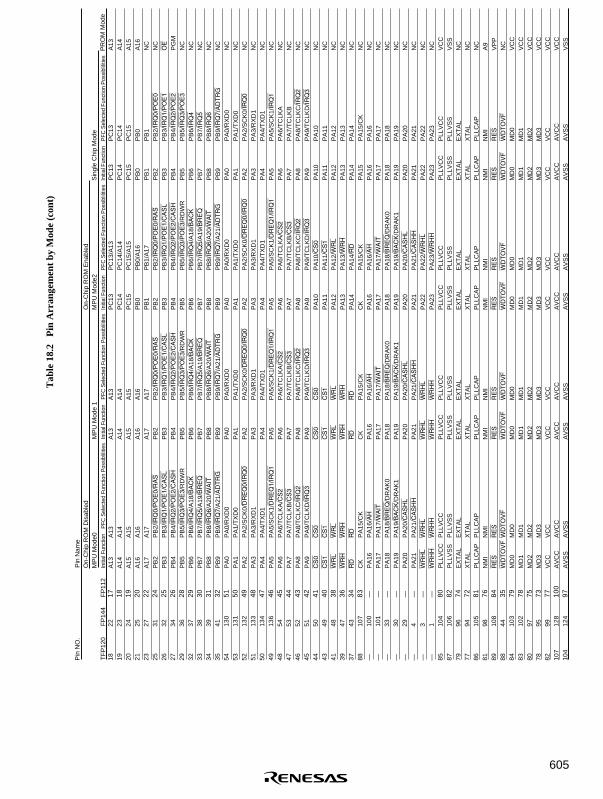
605
22
23
24
25
27
31
32
34
36
37
38
39
41
130
131
132
133
134
136
54
53
52
51
50
49
48
47
43
107
100
101
33
30
29
4 3 1 104
106
96
94
105
98
108
44
103
102
97
95
99
128
124
17
18
19
20
22
24
25
26
28
29
30
31
32
51
50
49
48
47
46
45
44
43
42
41
40
38
36
34
83
—
—
—
—
—
—
—
—
80
82
74
72
81
76
84
35
79
78
75
73
77
100
97
A13
A
14
A15
A
16
A17
P
B2/
IRQ
0/P
OE
0/R
AS
P
B3/
IRQ
1/P
OE
1/C
AS
LP
B4/
IRQ
2/P
OE
2/C
AS
H
PB
5/IR
Q3/
PO
E3/
RD
WR
P
B6/
IRQ
4/A
18/B
AC
K
PB
7/IR
Q5/
A19
/BR
EQ
P
B8/
IRQ
6/A
20/W
AIT
P
B9/
IRQ
7/A
21/A
DTR
G
PA
0/R
XD
0P
A1/
TX
D0
PA
2/S
CK
0/D
RE
Q0/
IRQ
0P
A3/
RX
D1
PA
4/T
XD
1P
A5/
SC
K1/
DR
EQ
1/IR
Q1
PA
6/T
CLK
A/C
S2
PA
7/T
CLK
B/C
S3
PA
8/T
CLK
C/IR
Q2
PA
9/T
CLK
D/IR
Q3
CS
0C
S1
WR
LW
RH
R
D
PA
15/C
K
PA
16/A
H
PA
17/W
AIT
P
A18
/BR
EQ
/DR
AK
0P
A19
/BA
CK
/DR
AK
1P
A20
/CA
SH
LP
A21
/CA
SH
H
WR
HL
WR
HH
P
LLV
CC
P
LLV
SS
E
XT
AL
XT
AL
PLL
CA
P
NM
IR
ES
W
DTO
VF
MD
0M
D1
MD
2M
D3
VC
C
AV
CC
A
VS
S
PC
13
PC
14
PC
15
PB
0P
B1
PB
2P
B3
PB
4P
B5
PB
6P
B7
PB
8P
B9
PA
0P
A1
PA
2P
A3
PA
4P
A5
PA
6P
A7
PA
8P
A9
PA
10
PA
11
PA
12
PA
13
PA
14
CK
P
A16
P
A17
P
A18
P
A19
P
A20
P
A21
P
A22
P
A23
P
LLV
CC
P
LLV
SS
E
XT
AL
XT
AL
PLL
CA
P
NM
IR
ES
W
DTO
VF
MD
0M
D1
MD
2M
D3
VC
C
AV
CC
A
VS
S
PC
13/A
13
PC
14/A
14
PC
15/A
15
PB
0/A
16
PB
1/A
17
PB
2/IR
Q0/
PO
E0/
RA
S
PB
3/IR
Q1/
PO
E1/
CA
SL
PB
4/IR
Q2/
PO
E2/
CA
SH
P
B5/
IRQ
3/P
OE
3/R
DW
R
PB
6/IR
Q4/
A18
/BA
CK
P
B7/
IRQ
5/A
19/B
RE
Q
PB
8/IR
Q6/
A20
/WA
IT
PB
9/IR
Q7/
A21
/AD
TRG
P
A0/
RX
D0
PA
1/T
XD
0P
A2/
SC
K0/
DR
EQ
0/IR
Q0
PA
3/R
XD
1P
A4/
TX
D1
PA
5/S
CK
1/D
RE
Q1/
IRQ
1P
A6/
TC
LKA
/CS
2P
A7/
TC
LKB
/CS
3P
A8/
TC
LKC
/IRQ
2P
A9/
TC
LKD
/IRQ
3P
A10
/CS
0P
A11
/CS
1P
A12
/WR
LP
A13
/WR
H
PA
14/R
D
PA
15/C
K
PA
16/A
H
PA
17/W
AIT
P
A18
/BR
EQ
/DR
AK
0P
A19
/BA
CK
/DR
AK
1P
A20
/CA
SH
LP
A21
/CA
SH
H
PA
22/W
RH
LP
A23
/WR
HH
P
LLV
CC
P
LLV
SS
E
XT
AL
XT
AL
PLL
CA
P
NM
IR
ES
W
DTO
VF
MD
0M
D1
MD
2M
D3
VC
C
AV
CC
A
VS
S
PC
13
PC
14
PC
15
PB
0P
B1
PB
2P
B3
PB
4P
B5
PB
6P
B7
PB
8P
B9
PA
0P
A1
PA
2P
A3
PA
4P
A5
PA
6P
A7
PA
8P
A9
PA
10
PA
11
PA
12
PA
13
PA
14
PA
15
PA
16
PA
17
PA
18
PA
19
PA
20
PA
21
PA
22
PA
23
PLL
VC
C
PLL
VS
S
EX
TA
LX
TA
LP
LLC
AP
N
MI
RE
S
WD
TOV
FM
D0
MD
1M
D2
MD
3V
CC
A
VC
C
AV
SS
PC
13
PC
14
PC
15
PB
0P
B1
PB
2/IR
Q0/
PO
E0
PB
3/IR
Q1/
PO
E1
PB
4/IR
Q2/
PO
E2
PB
5/IR
Q3/
PO
E3
PB
6/IR
Q4
PB
7/IR
Q5
PB
8/IR
Q6
PB
9/IR
Q7/
AD
TRG
P
A0/
RX
D0
PA
1/T
XD
0P
A2/
SC
K0/
IRQ
0P
A3/
RX
D1
PA
4/T
XD
1P
A5/
SC
K1/
IRQ
1P
A6/
TC
LKA
P
A7/
TC
LKB
P
A8/
TC
LKC
/IRQ
2P
A9/
TC
LKD
/IRQ
3P
A10
P
A11
P
A12
P
A13
P
A14
P
A15
/CK
P
A16
P
A17
P
A18
P
A19
P
A20
P
A21
P
A22
P
A23
P
LLV
CC
P
LLV
SS
E
XT
AL
XT
AL
PLL
CA
P
NM
IR
ES
W
DTO
VF
MD
0M
D1
MD
2M
D3
VC
C
AV
CC
A
VS
S
A13
A
14
A15
A
16
NC
N
C
OE
P
GM
N
C
NC
N
C
NC
N
C
NC
N
C
NC
N
C
NC
N
C
NC
N
C
NC
N
C
NC
N
C
NC
N
C
NC
N
C
NC
N
C
NC
N
C
NC
N
C
NC
N
C
VC
C
VS
S
NC
N
C
NC
A
9V
PP
N
C
VC
C
VC
C
VC
C
VC
C
VC
C
VC
C
VS
S
A13
A
14
A15
A
16
A17
P
B2
PB
3P
B4
PB
5P
B6
PB
7P
B8
PB
9P
A0
PA
1P
A2
PA
3P
A4
PA
5P
A6
PA
7P
A8
PA
9C
S0
CS
1W
RL
WR
H
RD
C
K
PA
16
PA
17
PA
18
PA
19
PA
20
PA
21
WR
HL
WR
HH
P
LLV
CC
P
LLV
SS
E
XT
AL
XT
AL
PLL
CA
P
NM
IR
ES
W
DTO
VF
MD
0M
D1
MD
2M
D3
VC
C
AV
CC
A
VS
S
A13
A
14
A15
A
16
A17
P
B2
PB
3P
B4
PB
5P
B6
PB
7P
B8
PB
9P
A0
PA
1P
A2
PA
3P
A4
PA
5P
A6
PA
7P
A8
PA
9C
S0
CS
1W
RL
WR
H
RD
C
K
PA
16
PA
17
PA
18
PA
19
PA
20
PA
21
WR
HL
WR
HH
P
LLV
CC
P
LLV
SS
E
XT
AL
XT
AL
PLL
CA
P
NM
IR
ES
W
DTO
VF
MD
0M
D1
MD
2M
D3
VC
C
AV
CC
A
VS
S
Pin
Nam
e
FP
144
18
19
20
21
23
25
26
27
29
32
33
34
35
54
53
52
51
50
49
48
47
46
45
44
43
41
39
37
88
—
—
—
—
—
—
—
—
85
87
79
77
86
81
89
88
84
83
80
78
82
107
104
Pin
NO
.
TF
P12
0F
P11
2S
ingl
e C
hip
Mod
eM
PU
Mod
e0M
PU
Mod
e 1
MP
U M
ode2
On-
Chi
p R
OM
Ena
bled
PR
OM
Mod
eIn
itial
Fun
ctio
n
On-
Chi
p R
OM
Dis
able
d
PFC
Sel
ecte
d Fu
nctio
n P
ossi
blili
ties
Initi
al F
unct
ion
PFC
Sel
ecte
d Fu
nctio
n P
ossi
blili
ties
Initi
al F
unct
ion
PFC
Sel
ecte
d Fu
nctio
n P
ossi
blili
ties
Initi
al F
unct
ion
PFC
Sel
ecte
d Fu
nctio
n P
ossi
blili
ties
Tab
le 1
8.2
Pin
Arr
ange
men
t by
Mod
e (c
ont)

606
127
118
119
120
121
122
123
125
126
109
110
111
113
114
115
116
137
138
139
140
142
143
144
2 5
—
91
92
93
94
95
96
98
99
85
86
87
88
89
102
104
105
106
107
108
110
111
112
1 2
AV
RE
F
PF
0/A
N0
PF
1/A
N1
PF
2/A
N2
PF
3/A
N3
PF
4/A
N4
PF
5/A
N5
PF
6/A
N6
PF
7/A
N7
PE
0/T
IOC
0A/D
RE
Q0
PE
1/T
IOC
0B/D
RA
K0
PE
2/T
IOC
0C/D
RE
Q1
PE
3/T
IOC
0D/D
RA
K1
PE
4/T
IOC
1A
PE
5/T
IOC
1B
PE
6/T
IOC
2A
PE
7/T
IOC
2B
PE
8/T
IOC
3A
PE
9/T
IOC
3B
PE
10/T
IOC
3C
PE
11/T
IOC
3D
PE
12/T
IOC
4A
PE
13/T
IOC
4B/M
RE
S
PE
14/T
IOC
4C/D
AC
K0/
AH
P
E15
/TIO
C4D
/DA
CK
1/IR
QO
UT
AV
RE
F
PF
0/A
N0
PF
1/A
N1
PF
2/A
N2
PF
3/A
N3
PF
4/A
N4
PF
5/A
N5
PF
6/A
N6
PF
7/A
N7
PE
0/T
IOC
0A/D
RE
Q0
PE
1/T
IOC
0B/D
RA
K0
PE
2/T
IOC
0C/D
RE
Q1
PE
3/T
IOC
0D/D
RA
K1
PE
4/T
IOC
1A
PE
5/T
IOC
1B
PE
6/T
IOC
2A
PE
7/T
IOC
2B
PE
8/T
IOC
3A
PE
9/T
IOC
3B
PE
10/T
IOC
3C
PE
11/T
IOC
3D
PE
12/T
IOC
4A
PE
13/T
IOC
4B/M
RE
S
PE
14/T
IOC
4C/D
AC
K0/
AH
P
E15
/TIO
C4D
/DA
CK
1/IR
QO
UTA
VR
EF
P
F0/
AN
0P
F1/
AN
1P
F2/
AN
2P
F3/
AN
3P
F4/
AN
4P
F5/
AN
5P
F6/
AN
6P
F7/
AN
7P
E0
PE
1P
E2
PE
3P
E4
PE
5P
E6
PE
7P
E8
PE
9P
E10
P
E11
P
E12
P
E13
P
E14
P
E15
AV
RE
F
PF
0/A
N0
PF
1/A
N1
PF
2/A
N2
PF
3/A
N3
PF
4/A
N4
PF
5/A
N5
PF
6/A
N6
PF
7/A
N7
PE
0/T
IOC
0A
PE
1/T
IOC
0B
PE
2/T
IOC
0C
PE
3/T
IOC
0D
PE
4/T
IOC
1A
PE
5/T
IOC
1B
PE
6/T
IOC
2A
PE
7/T
IOC
2B
PE
8/T
IOC
3A
PE
9/T
IOC
3B
PE
10/T
IOC
3C
PE
11/T
IOC
3D
PE
12/T
IOC
4A
PE
13/T
IOC
4B/M
RE
S
PE
14/T
IOC
4C
PE
15/T
IOC
4D
VS
S
VS
S
VS
S
VS
S
VS
S
VS
S
VS
S
VS
S
NC
N
C
NC
N
C
NC
N
C
NC
N
C
NC
N
C
NC
N
C
NC
N
C
NC
C
E
AV
RE
F
PF
0/A
N0
PF
1/A
N1
PF
2/A
N2
PF
3/A
N3
PF
4/A
N4
PF
5/A
N5
PF
6/A
N6
PF
7/A
N7
PE
0P
E1
PE
2P
E3
PE
4P
E5
PE
6P
E7
PE
8P
E9
PE
10
PE
11
PE
12
PE
13
PE
14
PE
15
AV
RE
F
PF
0/A
N0
PF
1/A
N1
PF
2/A
N2
PF
3/A
N3
PF
4/A
N4
PF
5/A
N5
PF
6/A
N6
PF
7/A
N7
PE
0P
E1
PE
2P
E3
PE
4P
E5
PE
6P
E7
PE
8P
E9
PE
10
PE
11
PE
12
PE
13
PE
14
PE
15
Pin
Nam
e
FP
144
—
98
99
100
101
102
103
105
106
92
93
94
95
96
109
112
113
114
115
116
118
119
120
2 3Pin
NO
.
TF
P12
0F
P11
2S
ingl
e C
hip
Mod
eM
PU
Mod
e0M
PU
Mod
e 1
MP
U M
ode2
On-
Chi
p R
OM
Ena
bled
PR
OM
Mod
eIn
itial
Fun
ctio
n
On-
Chi
p R
OM
Dis
able
d
Tab
le 1
8.2
Pin
Arr
ange
men
t by
Mod
e (c
ont)
PFC
Sel
ecte
d Fu
nctio
n P
ossi
blili
ties
Initi
al F
unct
ion
PFC
Sel
ecte
d Fu
nctio
n P
ossi
blili
ties
Initi
al F
unct
ion
PFC
Sel
ecte
d Fu
nctio
n P
ossi
blili
ties
Initi
al F
unct
ion
PFC
Sel
ecte
d Fu
nctio
n P
ossi
blili
ties

607
18.2 Register Configuration
Table 18.3 summarizes the registers of the pin function controller.
Table 18.3 Pin Function Controller Registers
Name Abbreviation R/W Initial Value Address Access Size
Port A I/O register H PAIORH R/W H'0000 H'FFFF8384H'FFFF8385
8, 16, 32
Port A I/O register L PAIORL R/W H'0000 H'FFFF8386H'FFFF8387
8, 16, 32
Port A control register H PACRH R/W H'0000 H'FFFF8388H'FFFF8389
8, 16, 32
Port A control register L1 PACRL1 R/W H'0000*H'4000
H'FFFF838CH'FFFF838D
8, 16, 32
Port A control register L2 PACRL2 R/W H'0000 H'FFFF838EH'FFFF838F
8, 16, 32
Port B I/O register PBIOR R/W H'0000 H'FFFF8394H'FFFF8395
8, 16, 32
Port B control register 1 PBCR1 R/W H'0000 H'FFFF8398H'FFFF8399
8, 16, 32
Port B control register 2 PBCR2 R/W H'0000 H'FFFF839AH'FFFF839B
8, 16, 32
Port C I/O register PCIOR R/W H'0000 H'FFFF8396H'FFFF8397
8, 16, 32
Port C control register PCCR R/W H'0000 H'FFFF839CH'FFFF839D
8, 16, 32
Port D I/O register H PDIORH R/W H'0000 H'FFFF83A4H'FFFF83A5
8, 16, 32
Port D I/O register L PDIORL R/W H'0000 H'FFFF83A6H'FFFF83A7
8, 16, 32
Port D control register H1 PDCRH1 R/W H'0000 H'FFFF83A8H'FFFF83A9
8, 16, 32
Port D control register H2 PDCRH2 R/W H'0000 H'FFFF83AAH'FFFF83AB
8, 16, 32
Port D control register L PDCRL R/W H'0000 H'FFFF83ACH'FFFF83AD
8, 16, 32
Port E I/O register PEIOR R/W H'0000 H'FFFF83B4H'FFFF83B5
8, 16, 32
Port E control register 1 PECR1 R/W H'0000 H'FFFF83B8H'FFFF83B9
8, 16, 32
Port E control register 2 PECR2 R/W H'0000 H'FFFF83BAH'FFFF83BB
8, 16, 32
IRQOUT function controlregister
IFCR R/W H'0000 H'FFFF83C8H'FFFF83C9
8, 16, 32
Note: * The port A control register L1 initial value varies depending on the operating mode.

608
18.3 Register Descriptions
18.3.1 Port A I/O Register H (PAIORH)
The port A I/O register H (PAIORH) is a 16-bit read/write register that selects input or output forthe most significant 8 pins of port A. Bits PA23IOR–PA16IOR correspond to pins PA23/WRHH–PA16/AH. PAIORH is enabled when the port A pins function as general input/outputs (PA23–PA16). For other functions, it is disabled.
For port A pin functions PA23–PA16, a given pin in port A is an output pin if its correspondingPAIORH bit is set to 1, and an input pin if the bit is cleared to 0.
PAIORH is initialized to H'0000 by external power-on reset; however, it is not initialized formanual resets, reset by WDT, standby mode, or sleep mode, so the previous data is maintained.
The settings for this register are effective only for the 144-pin version. There are no correspondingpins for this register in the 112-pin and 120-pin versions. However, read/writes are possible.
Bit: 15 14 13 12 11 10 9 8
— — — — — — — —
Initial value: 0 0 0 0 0 0 0 0
R/W: R R R R R R R R
Bit: 7 6 5 4 3 2 1 0
PA23IOR
PA22IOR
PA21IOR
PA20IOR
PA19IOR
PA18IOR
PA17IOR
PA16IOR
Initial value: 0 0 0 0 0 0 0 0
R/W: R/W R/W R/W R/W R/W R/W R/W R/W

609
18.3.2 Port A I/O Register L (PAIORL)
The port A I/O register L (PAIORL) is a 16-bit read/write register that selects input or output forthe least significant 16 pins of port A. Bits PA15IOR–PA0IOR correspond to pins PA15/CK–PA0/RXD0. PAIORL is enabled when the port A pins function as general input/outputs (PA15–PA0), or with the serial clock (SCK1, SCK0). For other functions, it is disabled.
When the port A pin functions PA15–PA0 are SCK1, SCK0, a given pin in port A is an output pinif its corresponding PAIORL bit is set to 1, and an input pin if the bit is cleared to 0.
PAIORL is initialized to H'0000 by external power-on reset; however, it is not initialized formanual resets, reset by WDT, standby mode, or sleep mode, so the previous data is maintained.
Bit: 15 14 13 12 11 10 9 8
PA15IOR
PA14IOR
PA13IOR
PA12IOR
PA11IOR
PA10IOR
PA9IOR
PA8IOR
Initial value: 0 0 0 0 0 0 0 0
R/W: R/W R/W R/W R/W R/W R/W R/W R/W
Bit: 7 6 5 4 3 2 1 0
PA7IOR
PA6IOR
PA5IOR
PA4IOR
PA3IOR
PA2IOR
PA1IOR
PA0IOR
Initial value: 0 0 0 0 0 0 0 0
R/W: R/W R/W R/W R/W R/W R/W R/W R/W
18.3.3 Port A Control Register H (PACRH)
PACRH is a 16-bit read/write register that selects the multiplex pin function for the eight mostsignificant pins of port A. PACRH selects the PA23/WRHH–PA16/AH pin functions.
The eight most significant pins of port A have bus control signals (WRHH, WRHL, CASHH,CASHL, BACK, BREQ, WAIT, AH) and DMAC control signals (DRAK1, DRAK0), but thereare instances when the register settings that select these pin functions will be ignored. Refer totable 18.2, Pin Arrangement by Mode.
PACRH is initialized to H'0000 by external power-on reset but is not initialized for manual resets,reset by WDT, standby mode, or sleep mode, so the previous data is maintained.

610
The settings for this register are effective only for the 144-pin version. There are no correspondingpins for this register in the 112-pin and 120-pin versions. However, read/writes are possible.
Bit: 15 14 13 12 11 10 9 8
— PA23MD
— PA22MD
— PA21MD
— PA20MD
Initial value: 0 0 0 0 0 0 0 0
R/W: R R/W R R/W R R/W R R/W
Bit: 7 6 5 4 3 2 1 0
PA19MD1
PA19MD0
PA18MD1
PA18MD0
— PA17MD
— PA16MD
Initial value: 0 0 0 0 0 0 0 0
R/W: R/W R/W R/W R/W R R/W R R/W
• Bit 15—Reserved: This bit always reads as 0. The write value should always be 0.
• Bit 14—PA23 Mode (PA23MD): Selects the function of the PA23/WRHH pin.
Bit 14: PA23MD Description
0 General input/output (PA23) (initial value) (WRHH in on-chip ROM invalid mode)
1 Most significant byte write output (WRHH) (PA23 in single chip mode)
• Bit 13—Reserved: This bit always reads as 0. The write value should always be 0.
• Bit 12—PA22 Mode (PA22MD): Selects the function of the PA22/WRHL pin.
Bit 12: PA22MD Description
0 General input/output (PA22) (initial value) (WRHL in on-chip ROM invalid mode)
1 Write output (WRHL) (PA22 in single chip mode)
• Bit 11—Reserved: This bit always reads as 0. The write value should always be 0.
• Bit 10—PA21 Mode (PA21MD): Selects the function of the PA21/CASHH pin.
Bit 10: PA21MD Description
0 General input/output (PA21) (initial value)
1 Column address output (CASHH) (PA21 in single chip mode)
• Bit 9—Reserved: Always reads as 0. The write values should always be 0.

611
• Bit 8—PA20 Mode (PA20MD): Selects the function of the PA20/CASHL pin.
Bit 8: PA20MD Description
0 General input/output (PA20) (initial value)
1 Column address output (CASHL) (PA20 in single chip mode)
• Bits 7 and 6—PA19 Mode 1, 0 (PA19MD1 and PA19MD0): These bits select the function ofthe PA19/BACK/DRAK1 pin.
Bit 7:PA19MD1
Bit 6:PA19MD0 Description
0 0 General input/output (PA19) (initial value)
1 Bus right request acknowledge (BACK) (PA19 in single chipmode)
1 0 DREQ1 request received output (DRAK1) (PA19 in singlechip mode)
1 Reserved
• Bits 5 and 4—PA18 Mode 1, 0 (PA18MD1 and PA18MD0): These bits select the function ofthe PA18/BREQ/DRAK0 pin.
Bit 5:PA18MD1
Bit 4:PA18MD0 Description
0 0 General input/output (PA18) (initial value)
1 Bus right request input (BREQ) (PA18 in single chip mode)
1 0 DREQ0 request received output (DRAK0) (PA18 in singlechip mode)
1 Reserved
• Bit 3—Reserved: This bit always reads as 0. The write value should always be 0.
• Bit 2—PA17 Mode (PA17MD): Selects the function of the PA17/WAIT pin.
Bit 2: PA17MD Description
0 General input/output (PA17) (initial value)
1 Wait state request input (WAIT) (PA17 in single chip mode)
• Bit 1—Reserved: This bit always reads as 0. The write value should always be 0.

612
• Bit 0—PA16 Mode (PA16MD): Selects the function of the PA16/AH pin.
Bit 0: PA16MD Description
0 General input/output (PA16) (initial value)
1 Address hold output (AH) (PA16 in single chip mode)
18.3.4 Port A Control Registers L1, L2 (PACRL1 and PACRL2)
PACRL1 and PACRL2 are 16-bit read/write registers that select the functions of the leastsignificant sixteen multiplexed pins of port A. PACRL1 selects the function of the PA15/CK–PA8/TCLKC/IRQ2 pins of port A; PACRL2 selects the function of the PA7/TCLKB/CS3–PA0/RXD0 pins of port A.
Port A has bus control signals (RD, WRH, WRL, CS0–CS3, AH) and DMAC control signals(DREQ0–DREQ1), but there are instances when the register settings that select these pin functionswill be ignored, depending on the operation mode. Refer to table 18.2, Pin Arrangement by Mode,for details.
PACRL1 is initialized by external power-on reset to H'4000 in extended mode, and to H'0000 insingle chip mode. PACRL2 is initialized by external power-on reset to H'0000. Neither register isinitialized by manual resets, reset by WDT, standby mode, or sleep mode, so the previous data ismaintained.
Port A Control Register L1 (PACRL1):
Bit: 15 14 13 12 11 10 9 8
— PA15MD — PA14MD — PA13MD — PA12MD
Initial value: 0 0(1)* 0 0 0 0 0 0
R/W: R R/W R R/W R R/W R R/W
Bit: 7 6 5 4 3 2 1 0
— PA11MD — PA10MD PA9MD1 PA9MD0 PA8MD1 PA8MD0
Initial value: 0 0 0 0 0 0 0 0
R/W: R R/W R R/W R/W R/W R/W R/W
Note: * Bit 14 is initialized to 1 in extended mode.
• Bit 15—Reserved: This bit always reads as 0. The write value should always be 0.

613
• Bit 14—PA15 Mode (PA15MD): Selects the function of the PA15/CK pin.
Bit 14: PA15MD Description
0 General input/output (PA15) (single chip mode initial value)
1 Clock output (CK) (extended mode initial value)
• Bit 13—Reserved: This bit always reads as 0. The write value should always be 0.
• Bit 12—PA14 Mode (PA14MD): Selects the function of the PA14/RD pin.
Bit 12: PA14MD Description
0 General input/output (PA14) (initial value) (RD in on-chip ROM invalid mode)
1 Read output (RD) (PA14 in single chip mode)
• Bit 11—Reserved: This bit always reads as 0. The write value should always be 0.
• Bit 10—PA13 Mode (PA13MD): Selects the function of the PA13/WRH pin.
Bit 10: PA13MD Description
0 General input/output (PA13) (initial value) (WRH in on-chip ROM invalid mode)
1 Most significant side write output (WRH) (PA13 in single chip mode)
• Bit 9—Reserved: This bit always reads as 0. The write value should always be 0.
• Bit 8—PA12 Mode (PA12MD): Selects the function of the PA12/WRL pin.
Bit 8: PA12MD Description
0 General input/output (PA12) (initial value) (WRL in on-chip ROM invalid mode)
1 Least significant side write output (WRL) (PA12 in single chip mode)
• Bit 7—Reserved: This bit always reads as 0. The write value should always be 0.
• Bit 6—PA11 Mode (PA11MD): Selects the function of the PA11/CS1 pin.
Bit 6: PA11MD Description
0 General input/output (PA11) (initial value) (CS1 in on-chip ROM invalid mode)
1 Chip select output (CS1) (PA11 in single chip mode)
• Bit 5—Reserved: This bit always reads as 0. The write value should always be 0.

614
• Bit 4—PA10 Mode (PA10MD): Selects the function of the PA10/CS0 pin.
Bit 4: PA10MD Description
0 General input/output (PA10) (initial value) (CS0 in on-chip ROM invalid mode)
1 Chip select output (CS0) (PA10 in single chip mode)
• Bits 3 and 2—PA9 Mode 1, 0 (PA9MD1 and PA9MD0): These bits select the function of thePA9/TCLKD/IRQ3 pin.
Bit 3:PA9MD1
Bit 2:PA9MD0 Description
0 0 General input/output (PA9) (initial value)
1 MTU timer clock input (TCLKD)
1 0 Interrupt request input (IRQ3)
1 Reserved
• Bits 1 and 0—PA8 Mode 1, 0 (PA8MD1 and PA8MD0): These bits select the function of thePA8/TCLKC/IRQ2 pin.
Bit 1:PA8MD1
Bit 0:PA8MD0 Description
0 0 General input/output (PA8) (initial value)
1 MTU timer clock input (TCLKC)
1 0 Interrupt request input (IRQ2)
1 Reserved

615
Port A Control Register L2 (PACRL2):
Bit: 15 14 13 12 11 10 9 8
PA7MD1
PA7MD0
PA6MD1
PA6MD0
PA5MD1
PA5MD0
— PA4MD
Initial value: 0 0 0 0 0 0 0 0
R/W: R/W R/W R/W R/W R/W R/W R R/W
Bit: 7 6 5 4 3 2 1 0
— PA3MD PA2MD1
PA2MD0
— PA1MD — PA0MD
Initial value: 0 0 0 0 0 0 0 0
R/W: R R/W R/W R/W R R/W R R/W
• Bits 15 and 14—PA7 Mode 1, 0 (PA7MD1 and PA7MD0): These bits select the function ofthe PA7/TCLKB/CS3 pin.
Bit 15:PA7MD1
Bit 14:PA7MD0 Description
0 0 General input/output (PA7) (initial value)
1 MTU timer clock input (TCLKB)
1 0 Chip select output (CS3) (PA7 in single chip mode)
1 Reserved
• Bits 13 and 12—PA6 Mode 1, 0 (PA6MD1 and PA6MD0): These bits select the function ofthe PA6/TCLKA/CS2 pin.
Bit 13:PA6MD1
Bit 12:PA6MD0 Description
0 0 General input/output (PA6) (initial value)
1 MTU timer clock input (TCLKA)
1 0 Chip select output (CS2) (PA6 in single chip mode)
1 Reserved

616
• Bits 11 and 10—PA5 Mode 1, 0 (PA5MD1 and PA5MD0): These bits select the function ofthe PA5/SCK1/DREQ1/IRQ1 pin.
Bit 11:PA5MD1
Bit 10:PA5MD0 Description
0 0 General input/output (PA5) (initial value)
1 Serial clock input/output (SCK1)
1 0 DMA transfer request received input (DREQ1) (PA5 in singlechip mode)
1 Interrupt request input (IRQ1)
• Bit 9—Reserved: This bit always reads as 0. The write value should always be 0.
• Bit 8—PA4 Mode (PA4MD): Selects the function of the PA4/TxD1 pin.
Bit 8: PA4MD Description
0 General input/output (PA4) (initial value)
1 Transmit data output (TxD1)
• Bit 7—Reserved: This bit always reads as 0. The write value should always be 0.
• Bit 6—PA3 Mode (PA3MD): Selects the function of the PA3/RxD1 pin.
Bit 6: PA3MD Description
0 General input/output (PA3) (initial value)
1 Receive data input (RxD1)
• Bits 5 and 4—PA2 Mode 1, 0 (PA2MD1 and PA2MD0): These bits select the function of thePA2/SCK0/DREQ0/IRQ0 pin.
Bit 5:PA2MD1
Bit 4:PA2MD0 Description
0 0 General input/output (PA2) (initial value)
1 Serial clock input/output (SCK0)
1 0 DMA transfer request received input (DREQ0) (PA2 in singlechip mode)
1 Interrupt request input (IRQ0)
• Bit 3—Reserved: This bit always reads as 0. The write value should always be 0.
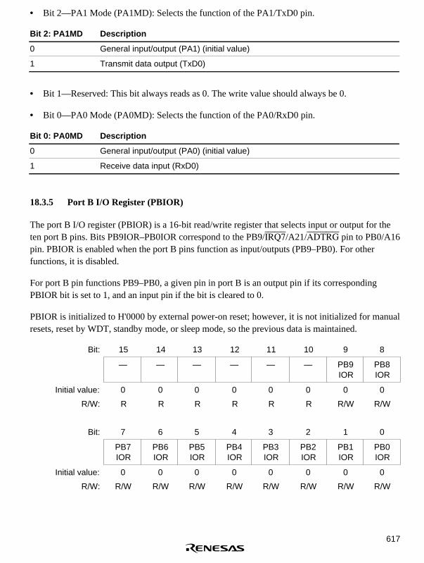
617
• Bit 2—PA1 Mode (PA1MD): Selects the function of the PA1/TxD0 pin.
Bit 2: PA1MD Description
0 General input/output (PA1) (initial value)
1 Transmit data output (TxD0)
• Bit 1—Reserved: This bit always reads as 0. The write value should always be 0.
• Bit 0—PA0 Mode (PA0MD): Selects the function of the PA0/RxD0 pin.
Bit 0: PA0MD Description
0 General input/output (PA0) (initial value)
1 Receive data input (RxD0)
18.3.5 Port B I/O Register (PBIOR)
The port B I/O register (PBIOR) is a 16-bit read/write register that selects input or output for theten port B pins. Bits PB9IOR–PB0IOR correspond to the PB9/IRQ7/A21/ADTRG pin to PB0/A16pin. PBIOR is enabled when the port B pins function as input/outputs (PB9–PB0). For otherfunctions, it is disabled.
For port B pin functions PB9–PB0, a given pin in port B is an output pin if its correspondingPBIOR bit is set to 1, and an input pin if the bit is cleared to 0.
PBIOR is initialized to H'0000 by external power-on reset; however, it is not initialized for manualresets, reset by WDT, standby mode, or sleep mode, so the previous data is maintained.
Bit: 15 14 13 12 11 10 9 8
— — — — — — PB9IOR
PB8IOR
Initial value: 0 0 0 0 0 0 0 0
R/W: R R R R R R R/W R/W
Bit: 7 6 5 4 3 2 1 0
PB7IOR
PB6IOR
PB5IOR
PB4IOR
PB3IOR
PB2IOR
PB1IOR
PB0IOR
Initial value: 0 0 0 0 0 0 0 0
R/W: R/W R/W R/W R/W R/W R/W R/W R/W

618
18.3.6 Port B Control Registers (PBCR1 and PBCR2)
PBCR1 and PBCR2 are 16-bit read/write registers that select the functions of the ten multiplexedpins of port B. PBCR1 selects the functions of the top two bits of port B; PBCR2 selects thefunctions of the bottom eight bits of port B.
Port B has bus control signals (RDWR, RAS, CASH, CASL, WAIT, BREQ, BACK) and addressoutputs (A21, A20, A19, A18, A17, A16), but there are instances when the register settings thatselect these pin functions will be ignored, depending on the operation mode. Refer to table 18.2,Pin Arrangement by Mode, for details.
PBCR1 and PBCR2 are both initialized to H'0000 by external power-on reset but are notinitialized for manual resets, reset by WDT, standby mode, or sleep mode, so the previous data ismaintained.
Port B Control Register 1 (PBCR1):
Bit: 15 14 13 12 11 10 9 8
— — — — — — — —
Initial value: 0 0 0 0 0 0 0 0
R/W: R R R R R R R R
Bit: 7 6 5 4 3 2 1 0
— — — — PB9MD1
PB9MD0
PB8MD1
PB8MD0
Initial value: 0 0 0 0 0 0 0 0
R/W: R R R R R/W R/W R/W R/W
• Bits 15-4—Reserved: These bits always read as 0. The write value should always be 0.
• Bits 3 and 2—PB9 Mode (PB9MD1 and PB9MD0): PB9MD1 and PB9MD0 select thefunction of the PB9/IRQ7/A21/ADTRG pin.
Bit 3: PB9MD1 Bit 2: PB9MD0 Description
0 0 General input/output (PB9) (initial value)
1 Interrupt request input (IRQ7)
1 0 Address output (A21) (PB9 in single chip mode)
1 A/D conversion trigger input (ADTRG)

619
• Bits 1 and 0—PB8 Mode (PB8MD1 and PB8MD0): PB8MD1 and PB8MD0 select thefunction of the PB8/IRQ6/A20/WAIT pin.
Bit 1: PB8MD1 Bit 0: PB8MD0 Description
0 0 General input/output (PB8) (initial value)
1 Interrupt request input (IRQ6)
1 0 Address output (A20) (PB8 in single chip mode)
1 Wait state request input (WAIT) (PB8 in single chipmode)
Port B Control Register 2 (PBCR2):
Bit: 15 14 13 12 11 10 9 8
PB7MD1 PB7MD0 PB6MD1 PB6MD0 PB5MD1 PB5MD0 PB4MD1 PB4MD0
Initial value: 0 0 0 0 0 0 0 0
R/W: R/W R/W R/W R/W R/W R/W R/W R/W
Bit: 7 6 5 4 3 2 1 0
PB3MD1 PB3MD0 PB2MD1 PB2MD0 — PB1MD — PB0MD
Initial value: 0 0 0 0 0 0 0 0
R/W: R/W R/W R/W R/W R R/W R R/W
• Bits 15 and 14—PB7 Mode (PB7MD1 and PB7MD0): PB7MD1 and PB7MD0 select thefunction of the PB7/IRQ5/A19/BREQ pin.
Bit 15:PB7MD1
Bit 14:PB7MD0 Description
0 0 General input/output (PB7) (initial value)
1 Interrupt request input (IRQ5)
1 0 Address output (A19) (PB7 in single chip mode)
1 Bus right request input (BREQ) (PB7 in single chip mode)

620
• Bits 13 and 12—PB6 Mode (PB6MD1 and PB6MD0): PB6MD1 and PB6MD0 select thefunction of the PB6/IRQ4/A18/BACK pin.
Bit 13:PB6MD1
Bit 12:PB6MD0 Description
0 0 General input/output (PB6) (initial value)
1 Interrupt request input (IRQ4)
1 0 Address output (A18) (PB6 in single chip mode)
1 Bus right request output (BACK) (PB6 in single chip mode)
• Bits 11 and 10—PB5 Mode (PB5MD1 and PB5MD0): PB5MD1 and PB5MD0 select thefunction of the PB5/IRQ3/POE3/RDWR pin.
Bit 11:PB5MD1
Bit 10:PB5MD0 Description
0 0 General input/output (PB5) (initial value)
1 Interrupt request input (IRQ3)
1 0 Port output enable (POE3)
1 Read/write output (RDWR)
• Bits 9 and 8—PB4 Mode (PB4MD1 and PB4MD0): PB4MD1 and PB4MD0 select thefunction of the PB4/IRQ2/POE2/CASH pin.
Bit 9: PB4MD1 Bit 8: PB4MD0 Description
0 0 General input/output (PB4) (initial value)
1 Interrupt request input (IRQ2)
1 0 Port output enable (POE2)
1 Column address strobe (CASH) (PB4 in single chip mode)
• Bits 7 and 6—PB3 Mode (PB3MD1 and PB3MD0): PB3MD1 and PB3MD0 select thefunction of the PB3/IRQ1/POE1/CASL pin.
Bit 7: PB3MD1 Bit 6: PB3MD0 Description
0 0 General input/output (PB3) (initial value)
1 Interrupt request input (IRQ1)
1 0 Port output enable (POE1)
1 Column address strobe (CASL) (PB3 in single chip mode)

621
• Bits 5 and 4—PB2 Mode (PB2MD1 and PB2MD0): PB2MD1 and PB2MD0 select thefunction of the PB2/IRQ0/POE0/RAS pin.
Bit 5: PB2MD1 Bit 4: PB2MD0 Description
0 0 General input/output (PB2) (initial value)
1 Interrupt request input (IRQ0)
1 0 Port output enable (POE0)
1 Row address strobe (RAS) (PB2 in single chip mode)
• Bit 3—Reserved: This bit always reads as 0. The write value should always be 0.
• Bit 2—PB1 Mode (PB1MD): Selects the function of the PB1/A17 pin.
Bit 2: PB1MD Description
0 General input/output (PB1) (initial value) (A17 in on-chip ROM invalid mode)
1 Address output (A17) (PB1 in single chip mode)
• Bit 1—Reserved: This bit always reads as 0. The write value should always be 0.
• Bit 0—PB0 Mode (PB0MD): Selects the function of the PB0/A16 pin.
Bit 0: PA0MD Description
0 General input/output (PB0) (initial value) (A16 in on-chip ROM invalid mode)
1 Address output (A16) (PB0 in single chip mode)

622
18.3.7 Port C I/O Register (PCIOR)
The port C I/O register (PCIOR) is a 16-bit read/write register that selects input or output for the16 port C pins. Bits PC15IOR–PC0IOR correspond to pins PC15/A15 to PC0/A0. PCIOR isenabled when the port C pins function as general input/outputs (PC15–PC0). For other functions,it is disabled.
When the port C pin functions are as PC15–PC0, a given pin in port C is an output pin if itscorresponding PCIOR bit is set to 1, and an input pin if the bit is cleared to 0.
PCIOR is initialized to H'0000 by external power-on reset; however, it is not initialized for manualresets, reset by WDT, standby mode, or sleep mode, so the previous values are maintained.
Bit: 15 14 13 12 11 10 9 8
PC15IOR
PC14IOR
PC13IOR
PC12IOR
PC11IOR
PC10IOR
PC9IOR
PC8IOR
Initial value: 0 0 0 0 0 0 0 0
R/W: R/W R/W R/W R/W R/W R/W R/W R/W
Bit: 7 6 5 4 3 2 1 0
PC7IOR
PC6IOR
PC5IOR
PC4IOR
PC3IOR
PC2IOR
PC1IOR
PC0IOR
Initial value: 0 0 0 0 0 0 0 0
R/W: R/W R/W R/W R/W R/W R/W R/W R/W
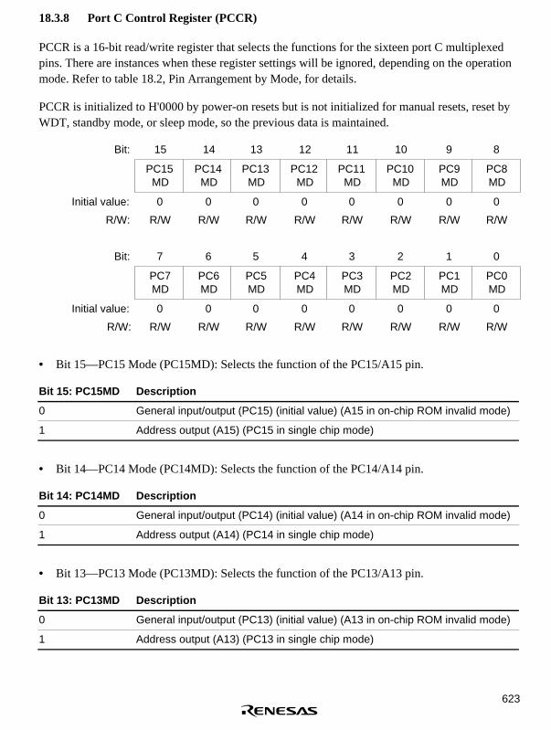
623
18.3.8 Port C Control Register (PCCR)
PCCR is a 16-bit read/write register that selects the functions for the sixteen port C multiplexedpins. There are instances when these register settings will be ignored, depending on the operationmode. Refer to table 18.2, Pin Arrangement by Mode, for details.
PCCR is initialized to H'0000 by power-on resets but is not initialized for manual resets, reset byWDT, standby mode, or sleep mode, so the previous data is maintained.
Bit: 15 14 13 12 11 10 9 8
PC15MD
PC14MD
PC13MD
PC12MD
PC11MD
PC10MD
PC9MD
PC8MD
Initial value: 0 0 0 0 0 0 0 0
R/W: R/W R/W R/W R/W R/W R/W R/W R/W
Bit: 7 6 5 4 3 2 1 0
PC7MD
PC6MD
PC5MD
PC4MD
PC3MD
PC2MD
PC1MD
PC0MD
Initial value: 0 0 0 0 0 0 0 0
R/W: R/W R/W R/W R/W R/W R/W R/W R/W
• Bit 15—PC15 Mode (PC15MD): Selects the function of the PC15/A15 pin.
Bit 15: PC15MD Description
0 General input/output (PC15) (initial value) (A15 in on-chip ROM invalid mode)
1 Address output (A15) (PC15 in single chip mode)
• Bit 14—PC14 Mode (PC14MD): Selects the function of the PC14/A14 pin.
Bit 14: PC14MD Description
0 General input/output (PC14) (initial value) (A14 in on-chip ROM invalid mode)
1 Address output (A14) (PC14 in single chip mode)
• Bit 13—PC13 Mode (PC13MD): Selects the function of the PC13/A13 pin.
Bit 13: PC13MD Description
0 General input/output (PC13) (initial value) (A13 in on-chip ROM invalid mode)
1 Address output (A13) (PC13 in single chip mode)

624
• Bit 12—PC12 Mode (PC12MD): Selects the function of the PC12/A12 pin.
Bit 12: PC12MD Description
0 General input/output (PC12) (initial value) (A12 in on-chip ROM invalid mode)
1 Address output (A12) (PC12 in single chip mode)
• Bit 11—PC11 Mode (PC11MD): Selects the function of the PC11/A11 pin.
Bit 11: PC11MD Description
0 General input/output (PC11) (initial value) (A11 in on-chip ROM invalid mode)
1 Address output (A11) (PC11 in single chip mode)
• Bit 10—PC10 Mode (PC10MD): Selects the function of the PC10/A10 pin.
Bit 10: PC10MD Description
0 General input/output (PC10) (initial value) (A10 in on-chip ROM invalid mode)
1 Address output (A10) (PC10 in single chip mode)
• Bit 9—PC9 Mode (PC9MD): Selects the function of the PC9/A9 pin.
Bit 9: PC9MD Description
0 General input/output (PC9) (initial value) (A9 in on-chip ROM invalid mode)
1 Address output (A9) (PC9 in single chip mode)
• Bit 8—PC8 Mode (PC8MD): Selects the function of the PC8/A8 pin.
Bit 8: PC8MD Description
0 General input/output (PC8) (initial value) (A8 in on-chip ROM invalid mode)
1 Address output (A8) (PC8 in single chip mode)
• Bit 7—PC7 Mode (PC7MD): Selects the function of the PC7/A7 pin.
Bit 7: PC7MD Description
0 General input/output (PC7) (initial value) (A7 in on-chip ROM invalid mode)
1 Address output (A7) (PC7 in single chip mode)
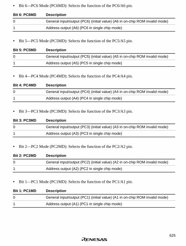
625
• Bit 6—PC6 Mode (PC6MD): Selects the function of the PC6/A6 pin.
Bit 6: PC6MD Description
0 General input/output (PC6) (initial value) (A6 in on-chip ROM invalid mode)
1 Address output (A6) (PC6 in single chip mode)
• Bit 5—PC5 Mode (PC5MD): Selects the function of the PC5/A5 pin.
Bit 5: PC5MD Description
0 General input/output (PC5) (initial value) (A5 in on-chip ROM invalid mode)
1 Address output (A5) (PC5 in single chip mode)
• Bit 4—PC4 Mode (PC4MD): Selects the function of the PC4/A4 pin.
Bit 4: PC4MD Description
0 General input/output (PC4) (initial value) (A4 in on-chip ROM invalid mode)
1 Address output (A4) (PC4 in single chip mode)
• Bit 3—PC3 Mode (PC3MD): Selects the function of the PC3/A3 pin.
Bit 3: PC3MD Description
0 General input/output (PC3) (initial value) (A3 in on-chip ROM invalid mode)
1 Address output (A3) (PC3 in single chip mode)
• Bit 2—PC2 Mode (PC2MD): Selects the function of the PC2/A2 pin.
Bit 2: PC2MD Description
0 General input/output (PC2) (initial value) (A2 in on-chip ROM invalid mode)
1 Address output (A2) (PC2 in single chip mode)
• Bit 1—PC1 Mode (PC1MD): Selects the function of the PC1/A1 pin.
Bit 1: PC1MD Description
0 General input/output (PC1) (initial value) (A1 in on-chip ROM invalid mode)
1 Address output (A1) (PC1 in single chip mode)

626
• Bit 0—PC0 Mode (PC0MD): Selects the function of the PC0/A0 pin.
Bit 0: PC0MD Description
0 General input/output (PC0) (initial value) (A0 in on-chip ROM invalid mode)
1 Address output (A0) (PC0 in single chip mode)
18.3.9 Port D I/O Register H (PDIORH)
The port D I/O register H (PDIORH) is a 16-bit read/write register that selects input or output forthe most significant sixteen port D pins. Bits PD31IOR–PD16IOR correspond to thePD31/D31/ADTRG pin to PD16/D16/IRQ0 pin. PDIORH is enabled when the port D pinsfunction as general input/outputs (PD31–PD16). For other functions, it is disabled.
For port D pin functions PD31–PD16, a given pin in port D is an output pin if its correspondingPDIORH bit is set to 1, and an input pin if the bit is cleared to 0.
PDIORH is initialized to H'0000 by external power-on reset; however, it is not initialized formanual resets, reset by WDT, standby mode, or sleep mode, so the previous data is maintained.
The settings for this register are effective only for the 144-pin version. There are no correspondingpins for this register in the 112-pin and 120-pin versions. However, read/writes are possible.
Bit: 15 14 13 12 11 10 9 8
PD31IOR
PD30IOR
PD29IOR
PD28IOR
PD27IOR
PD26IOR
PD25IOR
PD24IOR
Initial value: 0 0 0 0 0 0 0 0
R/W: R/W R/W R/W R/W R/W R/W R/W R/W
Bit: 7 6 5 4 3 2 1 0
PD23IOR
PD22IOR
PD21IOR
PD20IOR
PD19IOR
PD18IOR
PD17IOR
PD16IOR
Initial value: 0 0 0 0 0 0 0 0
R/W: R/W R/W R/W R/W R/W R/W R/W R/W

627
18.3.10 Port D I/O Register L (PDIORL)
The port D I/O register L (PDIORL) is a 16-bit read/write register that selects input or output forthe least significant sixteen port D pins. Bits PD15IOR–PD0IOR correspond to the PD15/D15 pinto PD0/D0 pin. PDIORL is enabled when the port D pins function as general input/outputs(PD15–PD0). For other functions, it is disabled.
For port D pin functions PD15–PD0, a given pin in port D is an output pin if its correspondingPDIORL bit is set to 1, and an input pin if the bit is cleared to 0.
PDIORL is initialized to H'0000 by external power-on reset; however, it is not initialized formanual resets, reset by WDT, standby mode, or sleep mode, so the previous data is maintained.
Bit: 15 14 13 12 11 10 9 8
PD15IOR
PD14IOR
PD13IOR
PD12IOR
PD11IOR
PD10IOR
PD9IOR
PD8IOR
Initial value: 0 0 0 0 0 0 0 0
R/W: R/W R/W R/W R/W R/W R/W R/W R/W
Bit: 7 6 5 4 3 2 1 0
PD7IOR
PD6IOR
PD5IOR
PD4IOR
PD3IOR
PD2IOR
PD1IOR
PD0IOR
Initial value: 0 0 0 0 0 0 0 0
R/W: R/W R/W R/W R/W R/W R/W R/W R/W
18.3.11 Port D Control Registers H1, H2 (PDCRH1 and PDCRH2)
PDCRH1 and PDCRH2 are 16-bit read/write registers that select the functions of the mostsignificant sixteen multiplexed pins of port D. PDCRH1 selects the functions of thePD31/D31/ADTRG–PD24/D24/DREQ0 pins of port D; PDCRH2 selects the functions of thePD23/D23/IRQ7–PD16/D16/IRQ0 pins of port D. There are instances when these register settingswill be ignored, depending on the operation mode. Refer to table 18.2, Pin Arrangement by Mode,for details.
The settings for this register are effective only for the 144-pin version. There are no correspondingpins for this register in the 112-pin and 120-pin versions. However, read/writes are possible.
PDCRH1 and PDCRH2 are both initialized to H'0000 by external power-on reset but are notinitialized for manual resets, reset by WDT, standby mode, or sleep mode, so the previous data ismaintained.

628
Port D Control Register H1 (PDCRH1):
Bit: 15 14 13 12 11 10 9 8
PD31MD1
PD31MD0
PD30MD1
PD30MD0
PD29MD1
PD29MD0
PD28MD1
PD28MD0
Initial value: 0 0 0 0 0 0 0 0
R/W: R/W R/W R/W R/W R/W R/W R/W R/W
Bit: 7 6 5 4 3 2 1 0
PD27MD1
PD27MD0
PD26MD1
PD26MD0
PD25MD1
PD25MD0
PD24MD1
PD24MD0
Initial value: 0 0 0 0 0 0 0 0
R/W: R/W R/W R/W R/W R/W R/W R/W R/W
• Bits 15 and 14—PD31 Mode 1, 0 (PD31MD1 and PD31MD0): These bits select the functionof the PD31/D31/ADTRG pin.
Bit 15:PD31MD1
Bit 14:PD31MD0 Description
0 0 General input/output (PD31) (initial value) (No ROM, D31 withCS0 = 32 bit width)
1 Data input/output (D31) (PD31 in single chip mode)
1 0 A/D conversion trigger input (ADTRG) (No ROM, D31 withCS0 = 32 bit width)
1 Reserved
• Bits 13 and 12—PD30 Mode 1, 0 (PD30MD1 and PD30MD0): These bits select the functionof the PD30/D30/IRQOUT pin.
Bit 13:PD30MD1
Bit 12:PD30MD0 Description
0 0 General input/output (PD30) (initial value) (No ROM, D30 withCS0 = 32 bit width)
1 Data input/output (D30) (PD30 in single chip mode)
1 0 Interrupt request received output (IRQOUT) (No ROM, D30with CS0 = 32 bit width. Reserved in single chip mode)
1 Reserved

629
• Bits 11 and 10—PD29 Mode 1, 0 (PD29MD1 and PD29MD0): These bits select the functionof the PD29/D29/CS3 pin.
Bit 11:PD29MD1
Bit 10:PD29MD0 Description
0 0 General input/output (PD29) (initial value) (D29 with no ROMand CS0 = 32 bit width)
1 Data input/output (D29) (PD29 in single chip mode)
1 0 Chip select output (CS3) (PD29 in single chip mode, D29 withno ROM and CS0 = 32 bit width)
1 Reserved
• Bits 9 and 8—PD28 Mode 1, 0 (PD28MD1 and PD28MD0): These bits select the function ofthe PD28/D28/CS2 pin.
Bit 9:PD28MD1
Bit 8:PD28MD0 Description
0 0 General input/output (PD28) (initial value) (D28 with no ROMand CS0 = 32 bit width)
1 Data input/output (D28) (PD28 in single chip mode)
1 0 Chip select output (CS2) (PD28 in single chip mode, and D28with no ROM and CS0 = 32 bit width)
1 Reserved
• Bits 7 and 6—PD27 Mode 1, 0 (PD27MD1 and PD27MD0): These bits select the function ofthe PD27/D27/DACK1 pin.
Bit 7:PD27MD1
Bit 6:PD27MD0 Description
0 0 General input/output (PD27) (initial value) (D27 with no ROMand CS0 = 32 bit width)
1 Data input/output (D27) (PD27 in single chip mode)
1 0 DMA transfer request received output (DACK1) (PD27 in singlechip mode, and D27 with no ROM and CS0 = 32 bit width)
1 Reserved

630
• Bits 5 and 4—PD26 Mode 1, 0 (PD26MD1 and PD26MD0): These bits select the function ofthe PD26/D26/DACK0 pin.
Bit 5:PD26MD1
Bit 4:PD26MD0 Description
0 0 General input/output (PD26) (initial value) (D26 with no ROMand CS0 = 32 bit width)
1 Data input/output (D26) (PD26 in single chip mode)
1 0 DMA transfer request received output (DACK0) (PD26 in singlechip mode, and D26 with no ROM and CS0 = 32 bit width)
1 Reserved
• Bits 3 and 2—PD25 Mode 1, 0 (PD25MD1 and PD25MD0): These bits select the function ofthe PD25/D25/DREQ1 pin.
Bit 3:PD25MD1
Bit 2:PD25MD0 Description
0 0 General input/output (PD25) (initial value) (D25 with no ROMand CS0 = 32 bit width)
1 Data input/output (D25) (PD25 in single chip mode)
1 0 DMA transfer request input (DREQ1) (PD25 in single chipmode, and D25 with no ROM and CS0 = 32 bit width)
1 Reserved
• Bits 1 and 0—PD24 Mode 1, 0 (PD24MD1 and PD24MD0): These bits select the function ofthe PD24/D24/DREQ0 pin.
Bit 1:PD24MD1
Bit 0:PD24MD0 Description
0 0 General input/output (PD24) (initial value) (D24 with no ROMand CS0 = 32 bit width)
1 Data input/output (D24) (PD24 in single chip mode)
1 0 DMA transfer request input (DREQ0) (PD24 in single chipmode, and D24 with no ROM and CS0 = 32 bit width)
1 Reserved

631
Port D Control Register H2 (PDCRH2):
Bit: 15 14 13 12 11 10 9 8
PD23MD1
PD23MD0
PD22MD1
PD22MD0
PD21MD1
PD21MD0
PD20MD1
PD20MD0
Initial value: 0 0 0 0 0 0 0 0
R/W: R/W R/W R/W R/W R/W R/W R/W R/W
Bit: 7 6 5 4 3 2 1 0
PD19MD1
PD19MD0
PD18MD1
PD18MD0
PD17MD1
PD17MD0
PD16MD1
PD16MD0
Initial value: 0 0 0 0 0 0 0 0
R/W: R/W R/W R/W R/W R/W R/W R/W R/W
• Bits 15 and 14—PD23 Mode 1, 0 (PD23MD1 and PD23MD0): These bits select the functionof the PD23/D23/IRQ7 pin.
Bit 15:PD23MD1
Bit 14:PD23MD0 Description
0 0 General input/output (PD23) (initial value) (D23 with no ROMand CS0 = 32 bit width)
1 Data input/output (D23) (PD23 in single chip mode)
1 0 Interrupt request input (IRQ7)
1 Reserved
• Bits 13 and 12—PD22 Mode 1, 0 (PD22MD1 and PD22MD0): These bits select the functionof the PD22/D22/IRQ6 pin.
Bit 13:PD22MD1
Bit 12:PD22MD0 Description
0 0 General input/output (PD22) (initial value) (D22 with no ROMand CS0 = 32 bit width)
1 Data input/output (D22) (PD22 in single chip mode)
1 0 Interrupt request input (IRQ6)
1 Reserved

632
• Bits 11 and 10—PD21 Mode 1, 0 (PD21MD1 and PD21MD0): These bits select the functionof the PD21/D21/IRQ5 pin.
Bit 11:PD21MD1
Bit 10:PD21MD0 Description
0 0 General input/output (PD21) (initial value) (D21 with no ROMand CS0 = 32 bit width)
1 Data input/output (D21) (PD21 in single chip mode)
1 0 Interrupt request input (IRQ5)
1 Reserved
• Bits 9 and 8—PD20 Mode 1, 0 (PD20MD1 and PD20MD0): These bits select the function ofthe PD20/D20/IRQ4 pin.
Bit 9:PD20MD1
Bit 8:PD20MD0 Description
0 0 General input/output (PD20) (initial value) (D20 with no ROMand CS0 = 32 bit width)
1 Data input/output (D20) (PD20 in single chip mode)
1 0 Interrupt request input (IRQ4)
1 Reserved
• Bits 7 and 6—PD19 Mode 1, 0 (PD19MD1 and PD19MD0): These bits select the function ofthe PD19/D19/IRQ3 pin.
Bit 7:PD19MD1
Bit 6:PD19MD0 Description
0 0 General input/output (PD19) (initial value) (D19 with no ROMand CS0 = 32 bit width)
1 Data input/output (D19) (PD19 in single chip mode)
1 0 Interrupt request input (IRQ3)
1 Reserved

633
• Bits 5 and 4—PD18 Mode 1, 0 (PD18MD1 and PD18MD0): These bits select the function ofthe PD18/D18/IRQ2 pin.
Bit 5:PD18MD1
Bit 4:PD18MD0 Description
0 0 General input/output (PD18) (initial value) (D18 with no ROMand CS0 = 32 bit width
1 Data input/output (D18) (PD18 in single chip mode)
1 0 Interrupt request input (IRQ2)
1 Reserved
• Bits 3 and 2—PD17 Mode 1, 0 (PD17MD1 and PD17MD0): These bits select the function ofthe PD17/D17/IRQ1 pin.
Bit 3:PD17MD1
Bit 2:PD17MD0 Description
0 0 General input/output (PD17) (initial value) (D17 with no ROMand CS0 = 32 bit width)
1 Data input/output (D17) (PD17 in single chip mode)
1 0 Interrupt request input (IRQ1)
1 Reserved
• Bits 1 and 0—PD16 Mode 1, 0 (PD16MD1 and PD16MD0): These bits select the function ofthe PD16/D16/IRQ0 pin.
Bit 1:PD16MD1
Bit 0:PD16MD0 Description
0 0 General input/output (PD16) (initial value) (D16 with no ROMand CS0 = 32 bit width)
1 Data input/output (D16) (PD16 in single chip mode)
1 0 Interrupt request input (IRQ0)
1 Reserved

634
18.3.12 Port D Control Register L (PDCRL)
PDCRL is a 16-bit read/write register that selects the multiplexed pin functions for the leastsignificant sixteen port D pins. There are instances when these register settings will be ignored,depending on the operation mode.
On-Chip ROM-Disabled Extended Mode:
• 144-pin version:
Mode 0 (16-bit bus): Port D pins are data I/O pins; PDCRL settings are disabled.
Mode 1 (32-bit bus): Port D pins are data I/O pins; PDCRL settings are disabled.
• 112-pin and 120-pin versions:
Mode 0 (8-bit bus): Port D pins are data I/O pins; PDCRL settings are disabled.
Mode 1 (16-bit bus): Port D pins are data I/O pins; PDCRL settings are disabled.
On-Chip ROM-Enabled Extended Mode: The port D pins are shared as data I/O pins andgeneral I/O pins; PDCRL settings are enabled.
Single Chip Mode: The port D pins are general I/O pins; PDCRL settings are disabled.
PDCRL is initialized to H'0000 by external power-on reset but is not initialized for manual resets,reset by WDT, standby mode, or sleep mode, so the previous data is maintained.
Port D Control Register L (PDCRL)
Bit: 15 14 13 12 11 10 9 8
PD15MD
PD14MD
PD13MD
PD12MD
PD11MD
PD10MD
PD9MD
PD8MD
Initial value: 0 0 0 0 0 0 0 0
R/W: R/W R/W R/W R/W R/W R/W R/W R/W
Bit: 7 6 5 4 3 2 1 0
PD7MD
PD6MD
PD5MD
PD4MD
PD3MD
PD2MD
PD1MD
PD0MD
Initial value: 0 0 0 0 0 0 0 0
R/W: R/W R/W R/W R/W R/W R/W R/W R/W

635
• Bit 15—PD15 Mode (PD15MD): Selects the function of the PD15/D15 pin.
Bit 15: PD15MD Description
0 General input/output (PD15) (initial value) (D15 in on-chip ROM invalid mode)
1 Data input/output (D15) (PD15 in single chip mode)
• Bit 14—PD14 Mode (PD14MD): Selects the function of the PD14/D14 pin.
Bit 14: PD14MD Description
0 General input/output (PD14) (initial value) (D14 in on-chip ROM invalid mode)
1 Data input/output (D14) (PD14 in single chip mode)
• Bit 13—PD13 Mode (PD13MD): Selects the function of the PD13/D13 pin.
Bit 13: PD13MD Description
0 General input/output (PD13) (initial value) (D13 in on-chip ROM invalid mode)
1 Data input/output (D13) (PD13 in single chip mode)
• Bit 12—PD12 Mode (PD12MD): Selects the function of the PD12/D12 pin.
Bit 12: PD12MD Description
0 General input/output (PD12) (initial value) (D12 in on-chip ROM invalid mode)
1 Data input/output (D12) (PD12 in single chip mode)
• Bit 11—PD11 Mode (PD11MD): Selects the function of the PD11/D11 pin.
Bit 11: PD11MD Description
0 General input/output (PD11) (initial value) (D11 in on-chip ROM invalid mode)
1 Data input/output (D11) (PD11 in single chip mode)
• Bit 10—PD10 Mode (PD10MD): Selects the function of the PD10/D10 pin.
Bit 10: PD10MD Description
0 General input/output (PD10) (initial value) (D10 in on-chip ROM invalid mode)
1 Data input/output (D10) (PD10 in single chip mode)

636
• Bit 9—PD9 Mode (PD9MD): Selects the function of the PD9/D9 pin.
Bit 9: PD9MD Description
0 General input/output (PD9) (initial value) (D9 in on-chip ROM invalid mode)
1 Data input/output (D9) (PD9 in single chip mode)
• Bit 8—PD8 Mode (PD8MD): Selects the function of the PD8/D8 pin.
Bit 8: PD8MD Description
0 General input/output (PD8) (initial value) (D8 in on-chip ROM invalid mode)
1 Data input/output (D8) (PD8 in single chip mode)
• Bit 7—PD7 Mode (PD7MD): Selects the function of the PD7/D7 pin.
Bit 7: PD7MD Description
0 General input/output (PD7) (initial value) (D7 in on-chip ROM invalid mode)
1 Data input/output (D7) (PD7 in single chip mode)
• Bit 6—PD6 Mode (PD6MD): Selects the function of the PD6/D6 pin.
Bit 6: PD6MD Description
0 General input/output (PD6) (initial value) (D6 in on-chip ROM invalid mode)
1 Data input/output (D6) (PD6 in single chip mode)
• Bit 5—PD5 Mode (PD5MD): Selects the function of the PD5/D5 pin.
Bit 5: PD5MD Description
0 General input/output (PD5) (initial value) (D5 in on-chip ROM invalid mode)
1 Data input/output (D5) (PD5 in single chip mode)
• Bit 4—PD4 Mode (PD4MD): Selects the function of the PD4/D4 pin.
Bit 4: PD4MD Description
0 General input/output (PD4) (initial value) (D4 in on-chip ROM invalid mode)
1 Data input/output (D4) (PD4 in single chip mode)

637
• Bit 3—PD3 Mode (PD3MD): Selects the function of the PD3/D3 pin.
Bit 3: PD3MD Description
0 General input/output (PD3) (initial value) (D3 in on-chip ROM invalid mode)
1 Data input/output (D3) (PD3 in single chip mode)
• Bit 2—PD2 Mode (PD2MD): Selects the function of the PD2/D2 pin.
Bit 2: PD2MD Description
0 General input/output (PD2) (initial value) (D2 in on-chip ROM invalid mode)
1 Data input/output (D2) (PD2 in single chip mode)
• Bit 1—PD1 Mode (PD1MD): Selects the function of the PD1/D1 pin.
Bit 1: PD1MD Description
0 General input/output (PD1) (initial value) (D1 in on-chip ROM invalid mode)
1 Data input/output (D1) (PD1 in single chip mode)
• Bit 0—PD0 Mode (PD0MD): Selects the function of the PD0/D0 pin.
Bit 0: PD0MD Description
0 General input/output (PD0) (initial value) (D0 in on-chip ROM invalid mode)
1 Data input/output (D0) (PD0 in single chip mode)

638
18.3.13 Port E I/O Register (PEIOR)
The port E I/O register (PEIOR) is a 16-bit read/write register that selects input or output for the16 port E pins. Bits PE15IOR–PE0IOR correspond to pins PE15/TIOC4D/DACK1/IRQOUT–PE0/TIOC0A/DREQ0. PEIOR is enabled when the port E pins function as general input/outputs(PE15–PE0) or TIOC pin of the MTU. For other functions, it is disabled.
When the port E pin functions are as PE15–PE0, or TIOC pin of the MTU, a given pin in port E isan output pin if its corresponding PEIOR bit is set to 1, and an input pin if the bit is cleared to 0.
PEIOR is initialized to H'0000 by external power-on reset; however, it is not initialized for manualresets, reset by WDT, standby mode, or sleep mode, so the previous data is maintained.
Bit: 15 14 13 12 11 10 9 8
PE15IOR
PE14IOR
PE13IOR
PE12IOR
PE11IOR
PE10IOR
PE9IOR
PE8IOR
Initial value: 0 0 0 0 0 0 0 0
R/W: R/W R/W R/W R/W R/W R/W R/W R/W
Bit: 7 6 5 4 3 2 1 0
PE7IOR
PE6IOR
PE5IOR
PE4IOR
PE3IOR
PE2IOR
PE1IOR
PE0IOR
Initial value: 0 0 0 0 0 0 0 0
R/W: R/W R/W R/W R/W R/W R/W R/W R/W
18.3.14 Port E Control Registers 1, 2 (PECR1 and PECR2)
PECR1 and PECR2 are 16-bit read/write registers that select the functions of the sixteenmultiplexed pins of port E. PECR1 selects the functions of the upper eight bit pins of port E;PECR2 selects the function of the lower eight bit pins of port E.
Port E has a bus control signal (AH) and DMAC control signals (DACK1, DACK0, DRAK1,DRAK0), but there are instances when the register settings that select these pin functions will beignored, depending on the operation mode. Refer to table 18.2, Pin Arrangement by Mode, fordetails.
PECR1 and PECR2 are both initialized to H'0000 by external power-on reset but are not initializedfor manual resets, reset by WDT, standby mode, or sleep mode, so the previous data is maintained.

639
Port E Control Register 1 (PECR1):
Bit: 15 14 13 12 11 10 9 8
PE15MD1
PE15MD0
PE14MD1
PE14MD0
PE13MD1
PE13MD0
— PE12MD
Initial value: 0 0 0 0 0 0 0 0
R/W: R/W R/W R/W R/W R/W R/W R R/W
Bit: 7 6 5 4 3 2 1 0
— PE11MD — PE10MD — PE9MD — PE8MD
Initial value: 0 0 0 0 0 0 0 0
R/W: R R/W R R/W R R/W R R/W
• Bits 15 and 14—PE15 Mode 1, 0 (PE15MD1 and PE15MD0): These bits select the function ofthe PE15/TIOC4D/DACK1/IRQOUT pin.
Bit 15:PE15MD1
Bit 14:PE15MD0 Description
0 0 Input/output (PE15) (initial value)
1 MTU input capture input/output compare output (TIOC4D)
1 0 DMAC request received output (DACK1) (PE15 in single chipmode)
1 Interrupt request output (IRQOUT)
(Reserved in single chip mode)
• Bits 13 and 12—PE14 Mode 1, 0 (PE14MD1 and PE14MD0): These bits select the function ofthe PE14/TIOC4C/DACK0/AH pin.
Bit 13:PE14MD1
Bit 12:PE14MD0 Description
0 0 Input/output (PE14) (initial value)
1 MTU input capture input/output compare output (TIOC4C)
1 0 DMAC request received output (DACK0) (PE14 in single chipmode)
1 Address hold output (AH) (PE14 in single chip mode)

640
• Bits 11 and 10—PE13 Mode 1, 0 (PE13MD1 and PE13MD0): These bits select the function ofthe PE13/TIOC4B/MRES pin.
Bit 11:PE13MD1
Bit 10:PE13MD0 Description
0 0 General input/output (PE13) (initial value)
1 MTU input capture input/output compare output (TIOC4B)
1 0 Manual reset input (MRES)
1 Reserved
• Bit 9—Reserved: This bit always reads as 0. The write values should always be 0.
• Bit 8—PE12 Mode (PE12MD): Selects the function of the PE12/TIOC4A pin.
Bit 8: PE12MD Description
0 General input/output (PE12) (initial value)
1 MTU input capture input/output compare output (TIOC4A)
• Bit 7—Reserved: This bit always reads as 0. The write values should always be 0.
• Bit 6—PE11 Mode (PE11MD): Selects the function of the PE11/TIOC3D pin.
Bit 6: PE11MD Description
0 General input/output (PE11) (initial value)
1 MTU input capture input/output compare output (TIOC3D)
• Bit 5—Reserved: This bit always reads as 0. The write values should always be 0.
• Bit 4—PE10 Mode (PE10MD): Selects the function of the PE10/TIOC3C pin.
Bit 4: PE10MD Description
0 General input/output (PE10) (initial value)
1 MTU input capture input/output compare output (TIOC3C)
• Bit 3—Reserved: This bit always reads as 0. The write values should always be 0.

641
• Bit 2—PE9 Mode (PE9MD): Selects the function of the PE9/TIOC3B pin.
Bit 2: PE9MD Description
0 General input/output (PE9) (initial value)
1 MTU input capture input/output compare output (TIOC3B)
• Bit 1—Reserved: This bit always reads as 0. The write values should always be 0.
• Bit 0—PE8 Mode (PE8MD): Selects the function of the PE8/TIOC3A pin.
Bit 0: PE8MD Description
0 General input/output (PE8) (initial value)
1 MTU input capture input/output compare output (TIOC3A)
Port E Control Register 2 (PECR2):
Bit: 15 14 13 12 11 10 9 8
— PE7MD — PE6MD — PE5MD — PE4MD
Initial value: 0 0 0 0 0 0 0 0
R/W: R R/W R R/W R R/W R R/W
Bit: 7 6 5 4 3 2 1 0
PE3MD1
PE3MD0
PE2MD1
PE2MD0
PE1MD1
PE1MD0
PE0MD1
PE0MD0
Initial value: 0 0 0 0 0 0 0 0
R/W: R/W R/W R/W R/W R/W R/W R/W R/W
• Bit 15—Reserved: This bit always reads as 0. The write value should always be 0.
• Bit 14—PE7 Mode (PE7MD): Selects the function of the PE7/TIOC2B pin.
Bit 14: PE7MD Description
0 General input/output (PE7) (initial value)
1 MTU input capture input/output compare output (TIOC2B)
• Bit 13 —Reserved: This bit always reads as 0. The write value should always be 0.

642
• Bit 12—PE6 Mode (PE6MD): Selects the function of the PE6/TIOC2A pin.
Bit 12: PE6MD Description
0 General input/output (PE6) (initial value)
1 MTU input capture input/output compare output (TIOC2A)
• Bit 11—Reserved: This bit always reads as 0. The write value should always be 0.
• Bit 10—PE5 Mode (PE5MD): Selects the function of the PE5/TIOC1B pin.
Bit 10: PE5MD Description
0 General input/output (PE5) (initial value)
1 MTU input capture input/output compare output (TIOC1B)
• Bit 9—Reserved: This bit always reads as 0. The write value should always be 0.
• Bit 8—PE4 Mode (PE4MD): Selects the function of the PE4/TIOC1A pin.
Bit 8: PE4MD Description
0 General input/output (PE4) (initial value)
1 MTU input capture input/output compare output (TIOC1A)
• Bits 7 and 6—PE3 Mode 1, 0 (PE3MD1 and PE3MD0): These bits select the function of thePE3/TIOC0D/DRAK1 pin.
Bit 7:PE3MD1
Bit 6:PE3MD0 Description
0 0 General input/output (PE3) (initial value)
1 MTU input capture input/output compare output (TIOC0D)
1 0 DREQ1 request received output (DRAK1) (PE3 in single chipmode)
1 Reserved

643
• Bits 5 and 4—PE2 Mode 1, 0 (PE2MD1 and PE2MD0): These bits select the function of thePE2/TIOC0C/DREQ1 pin.
Bit 5:PE2MD1
Bit 4:PE2MD0 Description
0 0 General input/output (PE2) (initial value)
1 MTU input capture input/output compare output (TIOC0C)
1 0 DREQ1 request receive input (PE2 in single chip mode)
1 Reserved
• Bits 3 and 2—PE1 Mode 1, 0 (PE1MD1 and PE1MD0): These bits select the function of thePE1/TIOC0B/DRAK0 pin.
Bit 3:PE1MD1
Bit 2:PE1MD0 Description
0 0 General input/output (PE1) (initial value)
1 MTU input capture input/output compare output (TIOC0B)
1 0 DREQ0 request received output (DRAK0) (PE1 in single chipmode)
1 Reserved
• Bits 1 and 0—PE0 Mode 1, 0 (PE0MD1 and PE0MD0): These bits select the function of thePE0/TIOC0A/DREQ0 pin.
Bit 1:PE0MD1
Bit 0:PE0MD0 Description
0 0 General input/output (PE0) (initial value)
1 MTU input capture input/output compare output (TIOC0A)
1 0 DREQ0 request receive input (PE0 in single chip mode)
1 Reserved
18.3.15 IRQOUT Function Control Register (IFCR)
The IFCR is a 16-bit read/write register used to control output when the multiplexed pins areestablished as IRQOUT outputs by the port D control register (PDCRH1) or port E control register(PECR1). When PDCRH1 or PECR1 are set for any other function, the settings of this registerhave no effect on the pin functions.

644
The IFCR is initialized to H'0000 by external power-on reset but is not initialized for manualresets, reset by WDT, standby mode, or sleep mode, so the previous data is maintained.
Bit: 15 14 13 12 11 10 9 8
— — — — — — — —
Initial value: 0 0 0 0 0 0 0 0
R/W: R R R R R R R R
Bit: 7 6 5 4 3 2 1 0
— — — — IRQMD3
IRQMD2
IRQMD1
IRQMD0
Initial value: 0 0 0 0 0 0 0 0
R/W: R R R R R/W R/W R/W R/W
• Bits 3 and 2—IRQOUT Mode 3, 2 (IRQMD3 and IRQMD2): These bits select the IRQOUTpin function when the PDCRH1 bits 13 and 12 (PD30MD1, PD30MD0) are set to (1, 0). Thesebit settings are effective only for the 144 pin version. Reads and writes are also possible in the112-pin and 120-pin versions, but they have no effect on the pin functions.
Bit 3: IRQMD3 Bit 2: IRQMD2 Description
0 0 Interrupt request received output (initial value)
1 Refresh signal output
1 0 Interrupt request received, or refresh signal output(which of the two is output depends on the operationstatus at the time)
1 Always high level output
• Bits 1 and 0—IRQOUT Mode 1, 0 (IRQMD1 and IRQMD0): These bits select the IRQOUTpin function when the PECR1 bits 1 and 0 (PE15MD1, PE15MD0) are set to (1, 1).
Bit 1: IRQMD1 Bit 0: IRQMD0 Description
0 0 Interrupt request received output (initial value)
1 Refresh signal output
1 0 Interrupt request received, or refresh signal output(which of the two is output depends on the operationstatus at the time)
1 Always high level output

645
18.4 Cautions on Use
For the I/O ports and pins with multiplexing of DREQ or IRQ, switching from the port input Lowlevel condition to IRQ or DREQ edge detection will detect the concerned edge.

646

647
Section 19 I/O Ports (I/O)
19.1 Overview
There are six ports, A, B, C, D, E, and F. The pins of the ports are multiplexed for use as general-purpose I/Os (the port F pins are general input) or for other functions. Use the pin functioncontroller (PFC) to select the function of multiplexed pins. The ports each have one data registerfor storing pin data. The initialize function after power-on reset differs depending on the operatingmode of each pin. See table 18.2, Pin Arrangement by Mode, for details.
19.2 Port A
There are two versions of port A:
• FP-112/TFP-120
• FP-144
In the FP-112 and TFP-120 versions, port A is a 16-pin input/output port, as listed in table 19.1.

648
Table 19.1 Port A, FP-112/TFP-120 Version
ROM Disabled ExtendedMode (Modes 0, 1)
ROM Enabled ExtendedMode (Mode 2) Single Chip Mode
PA15 (I/O)/CK (output) PA15 (I/O)/CK (output) PA15 (I/O)/CK (output)
RD (output) PA14 (I/O)/RD (output) PA14 (I/O)
WRH (output) PA13 (I/O)/WRH (output) PA13 (I/O)
WRL (output) PA12 (I/O)/WRL (output) PA12 (I/O)
CS1 (output) PA11 (I/O)/CS1 (output) PA11 (I/O)
CS0 (output) PA10 (I/O)/CS0 (output) PA10 (I/O)
PA9 (I/O)/TCLKD (input)/IRQ3(input)
PA9 (I/O)/TCLKD (input)/IRQ3(input)
PA9 (I/O)/TCLKD (input)/IRQ3(input)
PA8 (I/O)/TCLKC (input)/IRQ2(input)
PA8 (I/O)/TCLKC (input)/IRQ2(input)
PA8 (I/O)/TCLKC (input)/IRQ2(input)
PA7 (I/O)/TCLKB (input)/CS3(output)
PA7 (I/O)/TCLKB (input)/CS3(output)
PA7 (I/O)/TCLKB (input)
PA6 (I/O)/TCLKA (input)/CS2(output)
PA6 (I/O)/TCLKA (input)/CS2(output)
PA6 (I/O)/TCLKA (input)
PA5 (I/O)/SCK1 (I/O)/DREQ1(input)/IRQ1 (input)
PA5 (I/O)/SCK1 (I/O)/DREQ1(input)/IRQ1 (input)
PA5 (I/O)/SCK1 (I/O)/IRQ1(input)
PA4 (I/O)/TXD1 (output) PA4 (I/O)/TXD1 (output) PA4 (I/O)/TXD1 (output)
PA3 (I/O)/RXD1 (input) PA3 (I/O)/RXD1 (input) PA3 (I/O)/RXD1 (input)
PA2 (I/O)/SCK0 (I/O)/DREQ0(input)/IRQ0 (input)
PA2 (I/O)/SCK0 (I/O)/DREQ0(input)/IRQ0 (input)
PA2 (I/O)/SCK0 (I/O)/IRQ0(input)
PA1 (I/O)/TXD0 (output) PA1 (I/O)/TXD0 (output) PA1 (I/O)/TXD0 (output)
PA0 (I/O)/RXD0 (input) PA0 (I/O)/RXD0 (input) PA0 (I/O)/RXD0 (input)
In the FP-144 version, port A is a 24-pin input/output port, as listed in table 19.2.

649
Table 19.2 Port A, FP-144 Version
ROM Disabled ExtendedMode (Modes 0, 1)
ROM Enabled ExtendedMode (Mode 2) Single Chip Mode
WRHH (output) PA23 (I/O)/WRHH (output) PA23 (I/O)
WRHL (output) PA22 (I/O)/WRHL (output) PA22 (I/O)
PA21 (I/O)/CASHH (output) PA21 (I/O)/CASHH (output) PA21 (I/O)
PA20 (I/O)/CASHL (output) PA20 (I/O)/CASHL (output) PA20 (I/O)
PA19 (I/O)/BACK (output)/DRAK1 (output)
PA19 (I/O)/BACK (output)/DRAK1 (output)
PA19 (I/O)
PA18 (I/O)/BREQ (input)/DRAK0 (output)
PA18 (I/O)/BREQ (input)/DRAK0 (output)
PA18 (I/O)
PA17 (I/O)/WAIT (input) PA17 (I/O)/WAIT (input) PA17 (I/O)
PA16 (I/O)/AH (output) PA16 (I/O)/AH (output) PA16 (I/O)
PA15 (I/O)/CK (output) PA15 (I/O)/CK (output) PA15 (I/O)/CK (output)
RD (output) PA14 (I/O)/RD (output) PA14 (I/O)
WRH (output) PA13 (I/O)/WRH (output) PA13 (I/O)
WRL (output) PA12 (I/O)/WRL (output) PA12 (I/O)
CS1 (output) PA11 (I/O)/CS1 (output) PA11 (I/O)
CS0 (output) PA10 (I/O)/CS0 (output) PA10 (I/O)
PA9 (I/O)/TCLKD (input)/IRQ3(input)
PA9 (I/O)/TCLKD (input)/IRQ3(input)
PA9 (I/O)/TCLKD (input)/IRQ3(input)
PA8 (I/O)/TCLKC (input)/IRQ2(input)
PA8 (I/O)/TCLKC (input)/IRQ2(input)
PA8 (I/O)/TCLKC (input)/IRQ2(input)
PA7 (I/O)/TCLKB (input)/CS3(output)
PA7 (I/O)/TCLKB (input)/CS3(output)
PA7 (I/O)/TCLKB (input)
PA6 (I/O)/TCLKA (input)/CS2(output)
PA6 (I/O)/TCLKA (input)/CS2(output)
PA6 (I/O)/TCLKA (input)
PA5 (I/O)/SCK1 (I/O)/DREQ1(input)/IRQ1 (input)
PA5 (I/O)/SCK1 (I/O)/DREQ1(input)/IRQ1 (input)
PA5 (I/O)/SCK1 (I/O)/IRQ1(input)
PA4 (I/O)/TXD1 (output) PA4 (I/O)/TXD1 (output) PA4 (I/O)/TXD1 (output)
PA3 (I/O)/RXD1 (input) PA3 (I/O)/RXD1 (input) PA3 (I/O)/RXD1 (input)
PA2 (I/O)/SCK0 (I/O)/DREQ0(input)/IRQ0 (input)
PA2 (I/O)/SCK0 (I/O)/DREQ0(input)/IRQ0 (input)
PA2 (I/O)/SCK0 (I/O)/IRQ0(input)
PA1 (I/O)/TXD0 (output) PA1 (I/O)/TXD0 (output) PA1 (I/O)/TXD0 (output)
PA0 (I/O)/RXD0 (input) PA0 (I/O)/RXD0 (input) PA0 (I/O)/RXD0 (input)

650
19.2.1 Register Configuration
Table 19.3 summarizes the port A register.
Table 19.3 Port A Register
Name Abbreviation R/W Initial Value Address Access Size
Port A data register H PADRH R/W H'0000 H'FFFF8380H'FFFF8381
8, 16, 32
Port A data register L PADRL R/W H'0000 H'FFFF8382H'FFFF8383
8, 16, 32
19.2.2 Port A Data Register H (PADRH)
PADRH is a 16-bit read/write register that stores data for port A. The bits PA23DR–PA16DRcorrespond to the PA23/WRHH–PA16/AH pins. When the pins are used as ordinary outputs, theywill output whatever value is written in the PADRH; when PADRH is read, the register value willbe output regardless of the pin status. When the pins are used as ordinary inputs, the pin statusrather than the register value is read directly when PADRH is read. When a value is written toPADRH, that value can be written into PADRH, but it will not affect the pin status. Table 19.4shows the read/write operations of the port A data register.
PADRH is initialized by an external power-on reset. However, PADRH is not initialized formanual reset, reset by WDT, standby mode, or sleep mode.
These register settings function only for the 144-pin version. There are no pins corresponding tothis register in the 112-pin version. However, read/writes are possible.
Bit: 15 14 13 12 11 10 9 8
— — — — — — — —
Initial value: 0 0 0 0 0 0 0 0
R/W: R R R R R R R R
Bit: 7 6 5 4 3 2 1 0
PA23DR PA22DR PA21DR PA20DR PA19DR PA18DR PA17DR PA16DR
Initial value: 0 0 0 0 0 0 0 0
R/W: R/W R/W R/W R/W R/W R/W R/W R/W

651
19.2.3 Port A Data Register L (PADRL)
PADRL is a 16-bit read/write register that stores data for port A. The bits PA15DR–PA0DRcorrespond to the PA15/CK–PA0/RXD0 pins. When the pins are used as ordinary outputs, theywill output whatever value is written in the PADRL; when PADRL is read, the register value willbe output regardless of the pin status. When the pins are used as ordinary inputs, the pin statusrather than the register value is read directly when PADRL is read. When a value is written toPADRL, that value can be written into PADRL, but it will not affect the pin status. Table 19.4shows the read/write operations of the port A data register.
PADRL is initialized by an external power-on reset. However, PADRL is not initialized formanual reset, reset by WDT, standby mode, or sleep mode.
Bit: 15 14 13 12 11 10 9 8
PA15DR PA14DR PA13DR PA12DR PA11DR PA10DR PA9DR PA8DR
Initial value: 0 0 0 0 0 0 0 0
R/W: R/W R/W R/W R/W R/W R/W R/W R/W
Bit: 7 6 5 4 3 2 1 0
PA7DR PA6DR PA5DR PA4DR PA3DR PA2DR PA1DR PA0DR
Initial value: 0 0 0 0 0 0 0 0
R/W: R/W R/W R/W R/W R/W R/W R/W R/W
Table 19.4 Read/Write Operation of the Port A Data Register (PADR)
PAIOR Pin Status Read Write
0 Ordinary input Pin status Can write to PADR, but it has no effect on pin status
Other function Pin status Can write to PADR, but it has no effect on pin status
1 Ordinary output PADR value Value written is output by pin
Other function PADR value Can write to PADR, but it has no effect on pin status

652
19.3 Port B
Port B is a 10-pin input/output port as listed in table 19.5.
Table 19.5 Port B
ROM Disabled ExtendedMode (Modes 0, 1)
ROM Enabled ExtendedMode (Mode 2) Single Chip Mode
PB9 (I/O)/IRQ7 (input)/A21(output)/ADTRG (input)
PB9 (I/O)/IRQ7 (input)/A21(output)/ADTRG (input)
PB9 (I/O)/IRQ7 (input)/ADTRG(input)
PB8 (I/O)/IRQ6 (input)/A20(output)/WAIT (input)
PB8 (I/O)/IRQ6 (input)/A20(output)/WAIT (input)
PB8 (I/O)/IRQ6 (input)
PB7 (I/O)/IRQ5 (input)/A19(output)/BREQ (input)
PB7 (I/O)/IRQ5 (input)/A19(output)/BREQ (input)
PB7 (I/O)/IRQ5 (input)
PB6 (I/O)/IRQ4 (input)/A18(output)/BACK (output)
PB6 (I/O)/IRQ4 (input)/A18(output)/BACK (input)
PB6 (I/O)/IRQ4 (input)
PB5 (I/O)/IRQ3 (input)/POE3(input)/RDWR (output)
PB5 (I/O)/IRQ3 (input)/POE3(input)/RDWR (output)
PB5 (I/O)/IRQ3 (input)/POE3(input)
PB4 (I/O)/IRQ2 (input)/POE2(input)/CASH (output)
PB4 (I/O)/IRQ2 (input)/POE2(input)/CASH (output)
PB4 (I/O)/IRQ2 (input)/POE2(input)
PB3 (I/O)/IRQ1 (input)/POE1(input)/CASL (output)
PB3 (I/O)/IRQ1 (input)/POE1(input)/CASL (output)
PB3 (I/O)/IRQ1 (input)/POE1(input)
PB2 (I/O)/IRQ0 (input)/POE0(input)/RAS (output)
PB2 (I/O)/IRQ0 (input)/POE0(input)/RAS (output)
PB2 (I/O)/IRQ0 (input)/POE0(input)
A17 (output) PB1 (I/O)/A17 (output) PB1 (I/O)
A16 (output) PB0 (I/O)/A16 (output) PB0 (I/O)
19.3.1 Register Configuration
Table 19.6 summarizes the port B register.
Table 19.6 Port B Register
Name Abbreviation R/W Initial Value Address Access Size
Port B data register PBDR R/W H'0000 H'FFFF8390H'FFFF8391
8, 16, 32

653
19.3.2 Port B Data Register (PBDR)
PBDR is a 16-bit read/write register that stores data for port B. The bits PB9DR–PB0DRcorrespond to the PB9/IRQ7/A21/ADTRG–PB0/A16 pins. When the pins are used as ordinaryoutputs, they will output whatever value is written in the PBDR; when PBDR is read, the registervalue will be read regardless of the pin status. When the pins are used as ordinary inputs, the pinstatus rather than the register value is read directly when PBDR is read. When a value is written toPBDR, that value can be written into PBDR, but it will not affect the pin status. Table 19.7 showsthe read/write operations of the port B data register.
PBDR is initialized by an external power-on reset. However, PBDR is not initialized for a manualreset, reset by WDT, standby mode, or sleep mode.
Bit: 15 14 13 12 11 10 9 8
— — — — — — PB9DR PB8DR
Initial value: 0 0 0 0 0 0 0 0
R/W: R R R R R R R/W R/W
Bit: 7 6 5 4 3 2 1 0
PB7DR PB6DR PB5DR PB4DR PB3DR PB2DR PB1DR PB0DR
Initial value: 0 0 0 0 0 0 0 0
R/W: R/W R/W R/W R/W R/W R/W R/W R/W
Table 19.7 Read/Write Operation of the Port B Data Register (PBDR)
PBIOR Pin Status Read Write
0 Ordinary input Pin status Can write to PBDR, but it has no effect on pin status
Other function Pin status Can write to PBDR, but it has no effect on pin status
1 Ordinary output PBDR value Value written is output by pin
Other function PBDR value Can write to PBDR, but it has no effect on pin status

654
19.4 Port C
Port C is a 16 pin input/output port as listed in table 19.8.
Table 19.8 Port C
ROM Disabled ExtendedMode (Modes 0, 1)
ROM Enabled ExtendedMode (Mode 2) Single Chip Mode
A15 (output) PC15 (I/O)/A15 (output) PC15 (I/O)
A14 (output) PC14 (I/O)/A14 (output) PC14 (I/O)
A13 (output) PC13 (I/O)/A13 (output) PC13 (I/O)
A12 (output) PC12 (I/O)/A12 (output) PC12 (I/O)
A11 (output) PC11 (I/O)/A11 (output) PC11 (I/O)
A10 (output) PC10 (I/O)/A10 (output) PC10 (I/O)
A9 (output) PC9 (I/O)/A9 (output) PC9 (I/O)
A8 (output) PC8 (I/O)/A8 (output) PC8 (I/O)
A7 (output) PC7 (I/O)/A7 (output) PC7 (I/O)
A6 (output) PC6 (I/O)/A6 (output) PC6 (I/O)
A5 (output) PC5 (I/O)/A5 (output) PC5 (I/O)
A4 (output) PC4 (I/O)/A4 (output) PC4 (I/O)
A3 (output) PC3 (I/O)/A3 (output) PC3 (I/O)
A2 (output) PC2 (I/O)/A2 (output) PC2 (I/O)
A1 (output) PC1 (I/O)/A1 (output) PC1 (I/O)
A0 (output) PC0 (I/O)/A0 (output) PC0 (I/O)
19.4.1 Register Configuration
Table 19.9 summarizes the port C register.
Table 19.9 Port C Register
Name Abbreviation R/W Initial Value Address Access Size
Port C data register PCDR R/W H'0000 H'FFFF8392H'FFFF8393
8, 16, 32

655
19.4.2 Port C Data Register (PCDR)
PCDR is a 16-bit read/write register that stores data for port C. The bits PC15DR–PC0DRcorrespond to the PC15/A15–PC0/A0 pins. When the pins are used as ordinary outputs, they willoutput whatever value is written in the PCDR; when PCDR is read, the register value will be readregardless of the pin status. When the pins are used as ordinary inputs, the pin status rather thanthe register value is read directly when PCDR is read. When a value is written to PCDR, that valuecan be written into PCDR, but it will not affect the pin status. Table 19.10 shows the read/writeoperations of the port C data register.
PCDR is initialized by an external power-on reset. However, PCDR is not initialized for a manualreset, reset by WDT, standby mode, or sleep mode.
Bit: 15 14 13 12 11 10 9 8
PC15DR PC14DR PC13DR PC12DR PC11DR PC10DR PC9DR PC8DR
Initial value: 0 0 0 0 0 0 0 0
R/W: R/W R/W R/W R/W R/W R/W R/W R/W
Bit: 7 6 5 4 3 2 1 0
PC7DR PC6DR PC5DR PC4DR PC3DR PC2DR PC1DR PC0DR
Initial value: 0 0 0 0 0 0 0 0
R/W: R/W R/W R/W R/W R/W R/W R/W R/W
Table 19.10 Read/Write Operation of the Port C Data Register (PCDR)
PCIOR Pin Status Read Write
0 Ordinary input Pin status Can write to PCDR, but it has no effect on pin status
Other function Pin status Can write to PCDR, but it has no effect on pin status
1 Ordinary output PCDR value Value written is output by pin
Other function PCDR value Can write to PCDR, but it has no effect on pin status

656
19.5 Port D
There are two versions of port D:
• FP-112
• FP-144
In the FP-112 version, port D is a 16-pin input/output port, as shown in table 19.11.
Table 19.11 Port D, FP-112 Version
Extended ModeWithout ROM(Mode 0)
Extended ModeWithout ROM(Mode 1)
Extended Mode WithROM (Mode 2) Single Chip Mode
D15 (I/O) D15 (I/O) PD15 (I/O)/D15 (I/O) PD15 (I/O)
D14 (I/O) D14 (I/O) PD14 (I/O)/D14 (I/O) PD14 (I/O)
D13 (I/O) D13 (I/O) PD13 (I/O)/D13 (I/O) PD13 (I/O)
D12 (I/O) D12 (I/O) PD12 (I/O)/D12 (I/O) PD12 (I/O)
D11 (I/O) D11 (I/O) PD11 (I/O)/D11 (I/O) PD11 (I/O)
D10 (I/O) D10 (I/O) PD10 (I/O)/D10 (I/O) PD10 (I/O)
D9 (I/O) D9 (I/O) PD9 (I/O)/D9 (I/O) PD9 (I/O)
D8 (I/O) D8 (I/O) PD8 (I/O)/D8 (I/O) PD8 (I/O)
D7 (I/O) D7 (I/O) PD7 (I/O)/D7 (I/O) PD7 (I/O)
D6 (I/O) D6 (I/O) PD6 (I/O)/D6 (I/O) PD6 (I/O)
D5 (I/O) D5 (I/O) PD5 (I/O)/D5 (I/O) PD5 (I/O)
D4 (I/O) D4 (I/O) PD4 (I/O)/D4 (I/O) PD4 (I/O)
D3 (I/O) D3 (I/O) PD3 (I/O)/D3 (I/O) PD3 (I/O)
D2 (I/O) D2 (I/O) PD2 (I/O)/D2 (I/O) PD2 (I/O)
D1 (I/O) D1 (I/O) PD1 (I/O)/D1 (I/O) PD1 (I/O)
D0 (I/O) D0 (I/O) PD0 (I/O)/D0 (I/O) PD0 (I/O)
In the FP-144 version, port D is a 32-pin input/output port, as listed in table 19.12.

657
Table 19.12 Port D, FP-144 Version
Extended ModeWithout ROM(Mode 0)
Extended ModeWithout ROM(Mode 1)
Extended Mode WithROM (Mode 2) Single Chip Mode
PD31 (I/O)/D31 (I/O)/ADTRG (input)
D31 (I/O) PD31 (I/O)/D31 (I/O)/ADTRG (input)
PD31 (I/O)/ADTRG(input)
PD30 (I/O)/D30 (I/O)/IRQOUT (output)
D30 (I/O) PD30 (I/O)/D30 (I/O)/IRQOUT (output)
PD30 (I/O)/IRQOUT(output)
PD29 (I/O)/D29 (I/O)/CS3 (output)
D29 (I/O) PD29 (I/O)/D29 (I/O)/CS3 (output)
PD29 (I/O)
PD28 (I/O)/D28 (I/O)/CS2 (output)
D28 (I/O) PD28 (I/O)/D28 (I/O)/CS2 (output)
PD28 (I/O)
PD27 (I/O)/D27 (I/O)/DACK1 (output)
D27 (I/O) PD27 (I/O)/D27 (I/O)/DACK1 (output)
PD27 (I/O)
PD26 (I/O)/D26 (I/O)/DACK0 (output)
D26 (I/O) PD26 (I/O)/D26 (I/O)/DACK0 (output)
PD26 (I/O)
PD25 (I/O)/D25 (I/O)/DREQ1 (input)
D25 (I/O) PD25 (I/O)/D25 (I/O)/DREQ1 (input)
PD25 (I/O)
PD24 (I/O)/D24 (I/O)/DREQ0 (input)
D24 (I/O) PD24 (I/O)/D24 (I/O)/DREQ0 (input)
PD24 (I/O)
PD23 (I/O)/D23 (I/O)/IRQ7 (input)
D23 (I/O) PD23 (I/O)/D23 (I/O)/IRQ7 (input)
PD23 (I/O)/IRQ7(input)
PD22 (I/O)/D22 (I/O)/IRQ6 (input)
D22 (I/O) PD22 (I/O)/D22 (I/O)/IRQ6 (input)
PD22 (I/O)/IRQ6(input)
PD21 (I/O)/D21 (I/O)/IRQ5 (input)
D21 (I/O) PD21 (I/O)/D21 (I/O)/IRQ5 (input)
PD21 (I/O)/IRQ5(input)
PD20 (I/O)/D20 (I/O)/IRQ4 (input)
D20 (I/O) PD20 (I/O)/D20 (I/O)/IRQ4 (input)
PD20 (I/O)/IRQ4(input)
PD19 (I/O)/D19 (I/O)/IRQ3 (input)
D19 (I/O) PD19 (I/O)/D19 (I/O)/IRQ3 (input)
PD19 (I/O)/IRQ3(input)
PD18 (I/O)/D18 (I/O)/IRQ2 (input)
D18 (I/O) PD18 (I/O)/D18 (I/O)/IRQ2 (input)
PD18 (I/O)/IRQ2(input)
PD17 (I/O)/D17 (I/O)/IRQ1 (input)
D17 (I/O) PD17 (I/O)/D17 (I/O)/IRQ1 (input)
PD17 (I/O)/IRQ1(input)
PD16 (I/O)/D16 (I/O)/IRQ0 (input)
D16 (I/O) PD16 (I/O)/D16 (I/O)/IRQ0 (input)
PD16 (I/O)/IRQ0(input)

658
Table 19.12 Port D, FP-144 Version (cont)
Extended ModeWithout ROM(Mode 0)
Extended ModeWithout ROM(Mode 1)
Extended Mode WithROM (Mode 2) Single Chip Mode
D15 (I/O) D15 (I/O) PD15 (I/O)/D15 (I/O) PD15 (I/O)
D14 (I/O) D14 (I/O) PD14 (I/O)/D14 (I/O) PD14 (I/O)
D13 (I/O) D13 (I/O) PD13 (I/O)/D13 (I/O) PD13 (I/O)
D12 (I/O) D12 (I/O) PD12 (I/O)/D12 (I/O) PD12 (I/O)
D11 (I/O) D11 (I/O) PD11 (I/O)/D11 (I/O) PD11 (I/O)
D10 (I/O) D10 (I/O) PD10 (I/O)/D10 (I/O) PD10 (I/O)
D9 (I/O) D9 (I/O) PD9 (I/O)/D9 (I/O) PD9 (I/O)
D8 (I/O) D8 (I/O) PD8 (I/O)/D8 (I/O) PD8 (I/O)
D7 (I/O) D7 (I/O) PD7 (I/O)/D7 (I/O) PD7 (I/O)
D6 (I/O) D6 (I/O) PD6 (I/O)/D6 (I/O) PD6 (I/O)
D5 (I/O) D5 (I/O) PD5 (I/O)/D5 (I/O) PD5 (I/O)
D4 (I/O) D4 (I/O) PD4 (I/O)/D4 (I/O) PD4 (I/O)
D3 (I/O) D3 (I/O) PD3 (I/O)/D3 (I/O) PD3 (I/O)
D2 (I/O) D2 (I/O) PD2 (I/O)/D2 (I/O) PD2 (I/O)
D1 (I/O) D1 (I/O) PD1 (I/O)/D1 (I/O) PD1 (I/O)
D0 (I/O) D0 (I/O) PD0 (I/O)/D0 (I/O) PD0 (I/O)
19.5.1 Register Configuration
Table 19.13 summarizes the port D register.
Table 19.13 Port D Register
Name Abbreviation R/W Initial Value Address Access Size
Port D data register H PDDRH R/W H'0000 H'FFFF83A0H'FFFF83A1
8, 16, 32
Port D data register L PDDRL R/W H'0000 H'FFFF83A2H'FFFF83A3
8, 16, 32

659
19.5.2 Port D Data Register H (PDDRH)
PDDRH is a 16-bit read/write register that stores data for port D. The bits PD31DR–PD16DRcorrespond to the PD31/D31/ADTRG–PD16/D16/IRQ0 pins. When the pins are used as ordinaryoutputs, they will output whatever value is written in the PDDRH; when PDDRH is read, theregister value will be read regardless of the pin status. When the pins are used as ordinary inputs,the pin status rather than the register value is read directly when PDDRH is read. When a value iswritten to PDDRH, that value can be written into PDDRH, but it will not affect the pin status.Table 19.14 shows the read/write operations of the port D data register.
PDDRH is initialized by an external power-on reset. However, PDDRH is not initialized for amanual reset, reset by WDT, standby mode, or sleep mode.
These register settings function only for the 144-pin version. There are no pins corresponding tothis register in the 112-pin version. However, read/writes are possible.
Bit: 15 14 13 12 11 10 9 8
PD31DR PD30DR PD29DR PD28DR PD27DR PD26DR PD25DR PD24DR
Initial value: 0 0 0 0 0 0 0 0
R/W: R/W R/W R/W R/W R/W R/W R/W R/W
Bit: 7 6 5 4 3 2 1 0
PD23DR PD22DR PD21DR PD20DR PD19DR PD18DR PD17DR PD16DR
Initial value: 0 0 0 0 0 0 0 0
R/W: R/W R/W R/W R/W R/W R/W R/W R/W

660
19.5.3 Port D Data Register L (PDDRL)
PDDRL is a 16-bit read/write register that stores data for port D. The bits PD15DR–PD0DRcorrespond to the PD15/D15–PD0/D0 pins. When the pins are used as ordinary outputs, they willoutput whatever value is written in the PDDRL; when PDDRL is read, the register value will beread regardless of the pin status. When the pins are used as ordinary inputs, the pin status ratherthan the register value is read directly when PDDRL is read. When a value is written to PDDRL,that value can be written into PDDRL, but it will not affect the pin status. Table 19.14 shows theread/write operations of the port D data register.
PDDRL is initialized by an external power-on reset. However, PDDRL is not initialized for amanual reset, reset by WDT, standby mode, or sleep mode.
Bit: 15 14 13 12 11 10 9 8
PD15DR PD14DR PD13DR PD12DR PD11DR PD10DR PD9DR PD8DR
Initial value: 0 0 0 0 0 0 0 0
R/W: R/W R/W R/W R/W R/W R/W R/W R/W
Bit: 7 6 5 4 3 2 1 0
PD7DR PD6DR PD5DR PD4DR PD3DR PD2DR PD1DR PD0DR
Initial value: 0 0 0 0 0 0 0 0
R/W: R/W R/W R/W R/W R/W R/W R/W R/W
Table 19.14 Read/Write Operation of the Port D Data Register (PDDR)
PDIOR Pin Status Read Write
0 Ordinary input Pin status Can write to PDDR, but it has no effect on pin status
Other function Pin status Can write to PDDR, but it has no effect on pin status
1 Ordinary output PDDR value Value written is output by pin
Other function PDDR value Can write to PDDR, but it has no effect on pin status

661
19.6 Port E
Port E is a 16-pin input/output port, as listed in table 19.15.
Table 19.15 Port E
Extended Modes (Modes 0, 1, 2) Single Chip Mode
PE15 (I/O)/TIOC4D (I/O)/DACK1(output)/IRQOUT (output)
PE15 (I/O)/TIOC4D (I/O)/IRQOUT (output)
PE14 (I/O)/TIOC4C (I/O)/DACK0 (output)/AH(output)
PE14 (I/O)/TIOC4C (I/O)
PE13 (I/O)/TIOC4B (I/O)/MRES (input) PE13 (I/O)/TIOC4B (I/O)/MRES (input)
PE12 (I/O)/TIOC4A (I/O) PE12 (I/O)/TIOC4A (I/O)
PE11 (I/O)/TIOC3D (I/O) PE11 (I/O)/TIOC3D (I/O)
PE10 (I/O)/TIOC3C (I/O) PE10 (I/O)/TIOC3C (I/O)
PE9 (I/O)/TIOC3B (I/O) PE9 (I/O)/TIOC3B (I/O)
PE8 (I/O)/TIOC3A (I/O) PE8 (I/O)/TIOC3A (I/O)
PE7 (I/O)/TIOC2B (I/O) PE7 (I/O)/TIOC2B (I/O)
PE6 (I/O)/TIOC2A (I/O) PE6 (I/O)/TIOC2A (I/O)
PE5 (I/O)/TIOC1B (I/O) PE5 (I/O)/TIOC1B (I/O)
PE4 (I/O)/TIOC1A (I/O) PE4 (I/O)/TIOC1A (I/O)
PE3 (I/O)/TIOC0D (I/O)/DRAK1 (output) PE3 (I/O)/TIOC0D (I/O)
PE2 (I/O)/TIOC0C (I/O)/DREQ1 (input) PE2 (I/O)/TIOC0C (I/O)
PE1 (I/O)/TIOC0B (I/O)/DRAK0 (output) PE1 (I/O)/TIOC0B (I/O)
PE0 (I/O)/TIOC0A (I/O)/DREQ0 (input) PE0 (I/O)/TIOC0A (I/O)
19.6.1 Register Configuration
Table 19.16 summarizes the port E register.
Table 19.16 Port E Register
Name Abbreviation R/W Initial Value Address Access Size
Port E data register PEDR R/W H'0000 H'FFFF83B0H'FFFF83B1
8, 16, 32

662
19.6.2 Port E Data Register (PEDR)
PEDR is a 16-bit read/write register that stores data for port E. The bits PE15DR–PE0DRcorrespond to the PE15/TIOC4D/DACK1/IRQOUT–PE0/TIOC0A/DREQ0 pins. When the pinsare used as ordinary outputs, they will output whatever value is written in the PEDR; when PEDRis read, the register value will be read regardless of the pin status. When the pins are used asordinary inputs, the pin status rather than the register value is read directly when PEDR is read.When a value is written to PEDR, that value can be written into PEDR, but it will not affect thepin status. Table 19.17 shows the read/write operations of the port E data register.
PEDR is initialized by a external power-on reset. However, PEDR is not initialized for a manualreset, reset by WDT, standby mode, or sleep mode, so the previous data is retained.
Bit: 15 14 13 12 11 10 9 8
PE15DR PE14DR PE13DR PE12DR PE11DR PE10DR PE9DR PE8DR
Initial value: 0 0 0 0 0 0 0 0
R/W: R/W R/W R/W R/W R/W R/W R/W R/W
Bit: 7 6 5 4 3 2 1 0
PE7DR PE6DR PE5DR PE4DR PE3DR PE2DR PE1DR PE0DR
Initial value: 0 0 0 0 0 0 0 0
R/W: R/W R/W R/W R/W R/W R/W R/W R/W
Table 19.17 Read/Write Operation of the Port E Data Register (PEDR)
PEIOR Pin Status Read Write
0 Ordinary input Pin status Can write to PEDR, but it has no effect on pin status
Other function Pin status Can write to PEDR, but it has no effect on pin status
1 Ordinary output PEDR value Value written is output by pin
Other function PEDR value Can write to PEDR, but it has no effect on pin status

663
19.7 Port F
Port F is an 8-pin input port. All modes are configured in the following way:
• PF7 (input)/AN7 (input)
• PF6 (input)/AN6 (input)
• PF5 (input)/AN5 (input)
• PF4 (input)/AN4 (input)
• PF3 (input)/AN3 (input)
• PF2 (input)/AN2 (input)
• PF1 (input)/AN1 (input)
• PF0 (input)/AN0 (input)
19.7.1 Register Configuration
Table 19.18 summarizes the port F register.
Table 19.18 Port F Register
Name Abbreviation R/W Initial Value Address Access Size
Port F data register PFDR R External pindependent
H'FFFF83B3 8
19.7.2 Port F Data Register (PFDR)
PFDR is an 8-bit read-only register that stores data for port F. The bits PF7DR–PF0DRcorrespond to the PF7/AN7–PF0/AN0 pins. There are no bits 15–8, so always access as eight bits.Any value written into these bits is ignored, and there is no effect on the status of the pins. Whenany of the bits are read, the pin status rather than the bit value is read directly. However, when anA/D converter analog input is being sampled, values of 1 are read out. Table 19.19 shows theread/write operations of the port F data register.
PFDR is not initialized by power-on resets, manual resets, standby mode, or sleep mode (the bitsalways reflect the pin status).
Bit: 7 6 5 4 3 2 1 0
PF7DR PF6DR PF5DR PF4DR PF3DR PF2DR PF1DR PF0DR
Initial value: * * * * * * * *
R/W: R R R R R R R R
Note: * Initial values are dependent on the status of the pins at the time of the reads.

664
Table 19.19 Read/Write Operation of the Port F Data Register (PFDR)
Pin I/O Pin Function Read Write
Input Ordinary Pin status is read Ignored (no effect on pin status)
ANn: analog input 1 is read Ignored (no effect on pin status)
n=7-0

665
Section 20 64/128/256kB Mask ROM
20.1 Overview
This LSI is available with 64 kbytes, 128 kbytes, or 256 kbytes of on-chip ROM. The on-chipROM is connected to the CPU, direct memory access controller (DMAC) and data transfercontroller (DTC) through a 32-bit data bus (figures 20.1, 20.2, and 20.3). The CPU, DMAC, andDTC can access the on-chip ROM in 8, 16, and 32-bit widths. Data in the on-chip ROM canalways be accessed in one cycle.
H'00000000
H'00000004
H'00000001
H'00000005
H'00000002
H'00000006
H'00000003
H'00000007
H'0000FFFC H'0000FFFD H'0000FFFE H'0000FFFF
On-chip ROM
Internal data bus (32 bits)
Figure 20.1 Mask ROM Block Diagram (64-kbyte Version)

666
H'00000000
H'00000004
H'00000001
H'00000005
H'00000002
H'00000006
H'00000003
H'00000007
H'0001FFFC H'0001FFFD H'0001FFFE H'0001FFFF
On-chip ROM
Internal data bus (32 bits)
Figure 20.2 Mask ROM Block Diagram (128-kbyte Version)
H'00000000
H'00000004
H'00000001
H'00000005
H'00000002
H'00000006
H'00000003
H'00000007
H'0003FFFC H'0003FFFD H'0003FFFE H'0003FFFF
On-chip ROM
Internal data bus (32 bits)
Figure 20.3 Mask ROM Block Diagram (256-kbyte Version)

667
The operating mode determines whether the on-chip ROM is valid or not. The operating mode isselected using mode-setting pins MD3–MD0 as shown in table 20.1. If you are using the on-chipROM, select mode 2 or mode 3; if you are not, select mode 0 or 1. The on-chip ROM is allocatedto addresses H'00000000–H'0000FFFF of memory area 0 for the 64-kbyte version, H'00000000–H'0001FFFF of memory area 0 for the 128-kbyte version and H'00000000–H'0003FFFF ofmemory area 0 for the 256-kbyte version.
Table 20.1 Operation Modes and ROM
Mode Setting Pin
Operation Mode MD3 MD2 MD1 MD0 Area 0
Mode 0 (MCU mode 0) * * 0 0 On-chip ROM invalid, external 8-bit space (112pin and 120 pin), external 16-bit space (144 pin)
Mode 1 (MCU mode 1) * * 0 1 On-chip ROM invalid, external 16-bit space (112pin and 120 pin), external 32-bit space (144 pin)
Mode 2 (MCU mode 2) * * 1 0 On-chip ROM valid, external space (bus width setwith bus state controller)
Mode 3 (MCU mode 3) * * 1 1 On-chip ROM valid, single-chip mode
0: Low1: High* : Refer to section 3, Operating Modes.

668

669
Section 21 128kB PROM
21.1 Overview
This LSI has 128 kbytes of on-chip PROM.The on-chip ROM is connected to the CPU, the directmemory access controller (DMAC) and the data transfer controller (DTC) through a 32-bit databus (figures 21.1). The CPU, DMAC, and DTC can access the on-chip ROM in 8, 16, and 32-bitwidths. Data in the on-chip ROM can always be accessed in one cycle.
H'00000000
H'00000004
H'00000001
H'00000005
H'00000002
H'00000006
H'00000003
H'00000007
H'0001FFFC H'0001FFFD H'0001FFFE H'0001FFFF
On-chip ROM
Internal data bus (32 bits)
Figure 21.1 PROM Block Diagram
The operating mode determines whether the on-chip ROM is valid or not. The operating mode isselected using mode-setting pins MD3–MD0 as shown in table 21.1. If you are using the on-chipROM, select mode 2 or mode 3; if you are not, select mode 0 or 1. The on-chip ROM is allocatedto addresses H'00000000–H'0001FFFF of memory area 0.

670
Table 21.1 Operating Modes and ROM
Mode Setting Pin
Operating Mode MD3 MD2 MD1 MD0 Area 0
Mode 0 (MCU mode 0) * * 0 0 On-chip ROM invalid, external 8-bit space (112 pinand 120 pin), external 16-bit space (144 pin)
Mode 1 (MCU mode 1) * * 0 1 On-chip ROM invalid, external 16-bit space (112pin and 120 pin), external 32-bit space (144 pin)
Mode 2 (MCU mode 2) * * 1 0 On-chip ROM valid, with an external space (buswidth setting is performed by the bus statecontroller)
Mode 3 (MCU mode 3) * * 1 1 On-chip ROM valid, single chip mode
Mode 7 (PROM mode) 1 1 1 1 —
0: Low1: High* : Refer to section 3, Operating Modes.
With the PROM version, programs can be written in the same manner as with an ordinaryEPROM by setting the LSI to PROM mode and using a standard EPROM writer.
21.2 PROM Mode
21.2.1 PROM Mode Settings
When programming the on-chip PROM, set the pins as shown in figure 21.2, 21.3, or 21.4, andperform the programming in PROM mode.
21.2.2 Socket Adapter Pin Correspondence and Memory Map
Connect the socket adapter to the SH7040 series chip as shown in figure 21.2 or 21.3. This willallow the on-chip PROM to be programmed in the same manner as an ordinary 32-pin EPROM(HN27C101). Figures 21.2, 21.3, and 21.4 show the correspondence between the SH7040 Seriespins and HN27C101 pins. Figure 21.5 is a memory map of the on-chip ROM.

671
HN27C101EPROM socketadapter
0.1 µF
(112-pin version)SH7042Pin namePin numberRES/VPP84
NMI76PD0/D070PD1/D169PD2/D268PD3/D367PD4/D466PD5/D564PD6/D663PD7/D762PC0/A04PC1/A15PC2/A26PC3/A37PC4/A48PC5/A59PC6/A610PC7/A7PC8/A8
11
PB3/RD1/POE1/CASL12
PC10/A1025
PC11/A1114
PC12/A121516
PC13/A13PC14/A14
17
PC15/A151819
PB0/A16PB4/IRQ2/POE2/CASH
20
VCCMD0
21, 37,65,77,103
PLLVCC/AVCC80, 100PLLCAP, PLLVSS, EXTAL 81, 82, 74
VSS
AVSS
3, 23, 27, 33, 39, 55,61, 71, 90, 101, 109
MD17978
MD275
MD37397
PF0/AN0–PF7/AN791–96,98, 99
26PE15/TIOC4D/DACK1/IRQOUT
PE14/TIOC4C/DACK0/AH2
PB5/IRQ3/POE3/RDWR
128
Pin numberPin name1VPP
26A913I/O014I/O115I/O217I/O318I/O419I/O520I/O621I/O712A011A110A29A38A47A56A65
27A7
24A8
23OE
25A10
4A11A12
2829
A13
3A14A15
231
A16PGM
2232
CE
16VCC
VPP:
A16–A0:I/O7–I/O0:
OE:PGM:
CE:
VSS
PROM programpower supply(12.5 V)Address inputData input/outputOutput enableProgram enableChip enable
100 Ω
0.1 µF
2 nF
Figure 21.2 SH7042 Pin and HN27C101 Pin Correspondence (112-Pin Version)

672
Pin number Pin name
89
81
75
74
73
72
71
69
68
67
5
6
7
8
9
10
11
12
13
26
15
16
17
18
19
20
21
27
3
2
29
22, 40, 70, 82, 111
84
83
80
85, 107
86, 87, 79
4, 24, 28, 36, 42
58, 66, 76, 97, 108, 117
98 to 103
105 to 106
104
78
RES/Vpp
NMI
PD0/D0
PD1/D1
PD2/D2
PD3/D3
PD4/D4
PD5/D5
PD6/D6
PD7/D7
PC0/A0
PC1/A1
PC2/A2
PC3/A3
PC4/A4
PC5/A5
PC6/A6
PC7/A7
PC8/A8
PB3/IRQ1/POE1/CASL
PC10/A10
PC11/A11
PC12/A12
PC13/A13
PC14/A14
PC15/A15
PB0/A16
PB4/IRQ2/POE2/CASH
PE15/TIOC4D/DACK1/IRQOUT
PE14/TIOC4C/DACK0/AH
PB5/IRQ3/POE3/RDWR
VCC
MD0
MD1
MD2
PLLVCC, AVCC
PLLCAP, PLLVSS, EXTAL
VSS
PF0/AN0 to PF5/AN5
PF6/AN6 to PF7/AN7
AVSS
MD3
Pin name Pin number
Vpp 1
A9 26
I/O0
I/O1
I/O2
I/O3
I/O4
I/O5
I/O6
I/O7
A0
A1
A2
A3
A4
A5
A6
A7
A8
OE
A10
A11
A12
A13
A14
A15
A16
PGM
CE
Vcc
Vss
13
14
15
17
18
19
20
21
12
11
10
9
8
7
6
5
27
24
23
25
4
28
29
3
2
31
22
32
16
SH7042 (120-pin version) HN27C101EPROM socketadapter
Vpp:
A16 to A0:I/O7 to I/O0:
OE:PGM:
CE:
PROM programpower supply(12.5 V)Address inputData input/outputOutput enableProgram enableChip enable
0.1 µF
2 nF
0.1 µF
100 Ω
Figure 21.3 SH7042 Pin and HN27C101 Pin Correspondence (120-Pin Version)

673
HN27C101(144-pin version)SH7043
Pin namePin numberRES/VPP108
NMI98PD0/D092PD1/D191PD2/D290PD3/D389PD4/D488PD5/D586PD6/D684PD7/D783PC0/A07PC1/A18PC2/A29PC3/A310PC4/A411PC5/A513PC6/A615PC7/A7PC8/A8
16
PB3/IRQ1/POE1/CASL17
PC10/A1032
PC11/A1119
PC12/A122021
PC13/A13PC14/A14
22
PC15/A152324
PB0/A16PB4/IRQ2/POE2/CASH
25
VCC
MD0
12, 26, 40, 63, 77, 85, 99, 112, 135
PLLVCC, AVCC, AVref104, 128, 127PLLCAP, PLLVSS, EXTAL 105, 106, 96
VSS
AVSS
6, 14, 28, 35, 42, 55, 61, 71, 79, 87, 93, 117, 129,
141
MD1103102
MD297
MD395124
PF0/AN0–PF7/AN7118–123, 125, 126
34PE15/TIOC4D/DACK1/IRQOUT
PE14/TIOC4D/DACK0/AH5
PB5/IRQ3/POE3/RDWR
236
Pin numberPin name1VPP26A913I/O014I/O115I/O217I/O318I/O419I/O520I/O621I/O712A011A110A29A38A47A56A6527
A7
24A8
23OE
25A10
4A11A12
2829
A13
3A14A15
231
A16PGM
2232
CE
16VCC
VSS
EPROM socketadapter
VPP:
A16–A0:I/O7–I/O0:
OE:PGM:
CE:
PROM programpower supply(12.5 V)Address inputData input/outputOutput enableProgram enableChip enable100 Ω
0.1 µF
0.1 µF
2 nF
Figure 21.4 SH7043 Pin and HN27C101 Pin Correspondence (144-Pin Version)

674
On-chipROM space
(area 0)
H'0000
H'1FFFF (128-kbyte version)
H'00000000
H'0001FFFF (128-kbyte version)
Address for MCU modes 0, 1, 2, 3
Address forPROM mode
Figure 21.5 On-Chip ROM Memory Map
21.3 PROM Programming
The PROM mode write/verify specifications are the same as those of the standard EPROMHN27C101. However, because the page program format is not supported, do not set the PROM writer to the page programming mode. PROM writers that only support page programming modecannot be used. When selecting a PROM writer, confirm that it supports the byte-by-byte high-speed, high-reliability programming format.
21.3.1 Programming Mode Selection
There are two on-chip PROM programming modes: write and verify (reads and confirms writtendata). The mode is selected by using the pins (table 21.2).
Table 21.2 PROM Programming Mode Selection
Pin
Mode CE OE PGM VPP VCC I/O7–I/O0 A16–A0
Write 0 1 0 VPP VCC Data input Address
Verify 0 0 1 Data output input
Programming 0 0 0 HighProhibited 0 1 1 impedance
1 0 0
1 1 1
Note: 0: low level, 1: high level, VPP: VPP level, VCC: VCC level.

675
21.3.2 Write/Verify and Electrical Characteristics
Write/Verify: Writing and verification can be done using an efficient high speed, high reliabilityprogramming format. This format allows data writing that is both fast and reliable withoutapplying voltage stress to the device. Figure 21.6 shows the basic flow of the high speed, highreliability programming format.

676
Start
Set EPROM writer towrite/verify mode
(VCC = 6.0 V ± 0.25 V,VPP = 12.5 V ± 0.3 V)
Address = 0
n = 0
n + 1 → n
Data write(tPW = 0.2 ms ± 5%)
Data write(tOPW = 0.2n ms)
Is verifyresult OK?
No
Yes
Finaladdress?
No
Yes
Set EPROMwriter to read mode
(VCC = 5.0 V ± 0.25 V,VPP = VCC)
All addressread results
OK?
No
Yes
End
No good
No
VCC: Power supplyVPP: PROM program power supplytPW: Initial programming pulse width
tOPW: Over-programming pulse width
n = 25?Yes
Address + 1 → address
< Preliminary >
Figure 21.6 High-Speed, High-Reliability Programming Basic Flow

677
Electrical Characteristics: Tables 21.3 and 21.4 show the electrical characteristics forprogramming. Figure 21.7 shows the timing.
Table 21.3 DC Characteristics (VCC = 6.0 V ± 0.25 V, VPP = 12.5 V ± 0.3 V, VSS = 0 V, Ta =25°C ± 5°C)
Item Pin Symbol Min Typ Max UnitMeasurementConditions
Input high-levelvoltage
I/O7–I/O0, A16–A0,OE, CE, PGM
VIH 2.4 — VCC + 0.3 V
Input low-levelvoltage
I/O7–I/O0, A16–A0,OE, CE, PGM
VIL –0.3 — 0.8 V
Output high-levelvoltage
I/O7–I/O0 VOH 2.4 — — V IOH = –200 µA
Output low-levelvoltage
I/O7–I/O0 VOL — — 0.45 V IOL = 1.6 mA
Input leak current I/O7–I/O0, A16–A0,OE, CE, PGM
| ILI | — — 2 µA VIN = 5.25 V/0.5 V
VCC current ICC — — 80 mA
VPP current IPP — — 80 mA
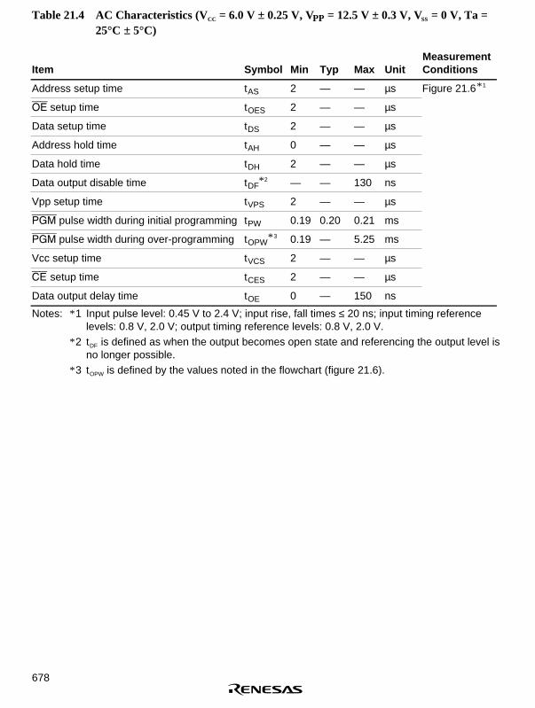
678
Table 21.4 AC Characteristics (VCC = 6.0 V ± 0.25 V, VPP = 12.5 V ± 0.3 V, VSS = 0 V, Ta =25°C ± 5°C)
Item Symbol Min Typ Max UnitMeasurementConditions
Address setup time tAS 2 — — µs Figure 21.6* 1
OE setup time tOES 2 — — µs
Data setup time tDS 2 — — µs
Address hold time tAH 0 — — µs
Data hold time tDH 2 — — µs
Data output disable time tDF* 2 — — 130 ns
Vpp setup time tVPS 2 — — µs
PGM pulse width during initial programming tPW 0.19 0.20 0.21 ms
PGM pulse width during over-programming tOPW* 3 0.19 — 5.25 ms
Vcc setup time tVCS 2 — — µs
CE setup time tCES 2 — — µs
Data output delay time tOE 0 — 150 ns
Notes: * 1 Input pulse level: 0.45 V to 2.4 V; input rise, fall times ≤ 20 ns; input timing referencelevels: 0.8 V, 2.0 V; output timing reference levels: 0.8 V, 2.0 V.
* 2 tDF is defined as when the output becomes open state and referencing the output level isno longer possible.
* 3 tOPW is defined by the values noted in the flowchart (figure 21.6).

679
Address
Data
VPP
VCC
CE
PGM
OE
Write Verify
tAH
Read data
tDFtDHtDS
tAS
tVPS
Write data
tVCS
tCES
tPW
(tOPW)*
tOES tOE
VPP
VCC
VCC + 1
VCC
Note: * tOPW is defined by the values noted in the flowchart (figure 19.6).
Figure 21.7 Write/Verify Timing
21.3.3 Cautions on Writing
1. Writes must always be done with the established voltage and timing. The write voltage(programming voltage) VPP is 12.5 V (when the EPROM writer is set for the HN27C101Hitachi specifications, VPP becomes 12.5 V). Devices will sometimes be destroyed if a voltagehigher than the rated one is applied. Pay particular attention to such phenomena as EPROMwriter overshoot.
2. Always confirm that the indices of the EPROM writer socket, socket adapter, and device are inagreement before programming. Devices will sometimes be destroyed due to excessive currentflow if these are not connected in the proper locations.
3. Do not touch the socket adapter or device during writing. Contact faults can sometimes causedevices to be improperly written.
4. Page programming mode writes are not possible. Always set to byte programming mode.

680
5. Terminate the writing if a write malfunction occurs in consecutive addresses. In such cases,check for problems in the EPROM writer and/or socket adapter. There are some cases wherewrite/verify will not be possible if using an EPROM writer with a high impedance powersupply system.
6. Use a EPROM writer that conforms to the socket adapter supported by this LSI.
21.3.4 Post-Write Reliability
High temperature biasing (or burn-in) of devices is recommended after writing in order to improvethe data retention characteristics. High temperature biasing is a method of screening thateliminates parts with faulty initial data retention by on-chip PROM memory cells within a shortperiod of time. Figure 21.8 shows the flow from the on-chip PROM programming includingscreening to the installation of the device on a board.
Program write/verify
Installation on board
Figure 21.5 (flowchart)
Unpowered high-temperature bias
(125–150°C, 24–48 hours)
Data read out and verify(VCC = 5.0 V)
Figure 21.8 Screening Flow
If there are any abnormalities in program write/verify or program read-out verification after hightemperature biasing, please contact a Renesas Technology technical representative.

681
Section 22 256kB Flash Memory (F-ZTAT)
22.1 Features
This LSI has 256 kbytes of on-chip flash memory. The features of the flash memory aresummarized below.
• Four flash memory operating modes
Program mode
Erase mode
Program-verify mode
Erase-verify mode
• Programming/erase methods
The flash memory is programmed 32 bytes at a time. Block erase (in single-block units) can beperformed. Block erasing can be performed as required on 1 kbyte, 28 kbyte, and 32 kbyteblocks.
• Programming/erase times
The flash memory programming time is 10 ms (typ.) for simultaneous 32-byte programming,equivalent to 300 µs (typ.) per byte, and the erase time is 100 ms (typ.) per block.
• Reprogramming capability
The flash memory can be reprogrammed up to 100 times.
• On-board programming modes
There are two modes in which flash memory can be programmed/erased/verified on-board:
Boot mode
User program mode
• Automatic bit rate adjustment
With data transfer in boot mode, this LSI’s bit rate can be automatically adjusted to match thetransfer bit rate of the host.
• Flash memory emulation in RAM
Flash memory programming can be emulated in real time by overlapping a part of RAM ontoflash memory.
• Protect modes
There are two protect modes, hardware and software, which allow protected status to bedesignated for flash memory program/erase/verify operations
• Programmer mode
Flash memory can be programmed/erased in programmer mode, using a PROM programmer,as well as in on-board programming mode.

682
22.2 Overview
22.2.1 Block Diagram
FLMCR2
EBR1
EBR2
RAMER
FLMCR1
Internal address bus
Internal data bus (32-bit)
Mod
ule
bus
Bus interface/controllerOperation mode
FWP pinMode pins
Flash memory(256kB)
LegendFLMCR1: Flash memory control register 1FLMCR2: Flash memory control register 2EBR1 : Block specification register 1EBR2 : Block specification register 2RAMER : RAM emulation register
Figure 22.1 Flash Memory Block Diagram

683
22.2.2 Mode Transition Diagram
When the mode pins and the FWP pin are set in the reset state and a reset start is executed, themicrocomputer enters one of the operating modes shown in figure 22.2. In user mode, flashmemory can be read but not programmed or erased.
Flash memory can be programmed and erased in boot mode, user program mode, and programmermode.
MD
1=0,
FW
P=
0
RE
S=
0
RES=0
FWP=0 FWP=1
*1
*1
*2
MD1=
1, F
WP=0
RES=0MD1=1, FWP=1
RES=0
Notes: Execute transition between the user mode and user program mode while the CPU is not programming or erasing the flash memory. *1 RAM emulation permitted*2 MD0=1, MD1=0, MD2=1, MD3=1
Reset state
User mode
User program mode
Boot mode
Programmer mode
On-board programming mode
Figure 22.2 Flash Memory Mode Transitions

684
22.2.3 Onboard Program Mode
Boot mode
New application program
New application program
New application program
Program
Program
ProgramProgram
LSI LSI
Boot program Boot program
LSI LSI
Boot program
Flash memory
Application version (old version)
Boot program
Flash memory Flash memory
Application version (old version)
RAM Flash memory RAM
RAM RAM
SCI1 SCI1
SCI1 SCI1
HOSTHOST
HOSTHOST
Boot program area
Boot program areaBoot program area
3. Initializing the flash memory To initialize (to H'FF) the flash memory, execute the erase program located in the boot program area (within RAM). During the boot mode, the entire flash memory is erased, regardless of blocks.
4. Writing the new application program Execute the program transferred to RAM from the host and write the new application program located at the transfer destination to the flash memory.
Erasing the flash memory
New application program
Program execution state
1. Initial state The old program version or data remains written
in the flash memory. The user should prepare the programming control program and new application program beforehand in the host.
2. Programming control program transfer When boot mode is entered, the boot program in
the LSI (originally incorporated in the chip) is started and the programming control program in the host is transferred to RAM via SCI communication. The boot program required for flash memory erasing is automatically transferred to the RAM boot program area.
Figure 22.3 Boot Mode
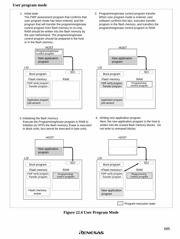
685
User program mode
3. Initializing the flash memory Execute the Programming/erase program in RAM to initialize (to H'FF) the flash memory. Erase is executed in block units, but cannot be executed in byte units.
HOST HOST
HOST HOSTProgramming/erase control program
New application program
New application program
New application program
LSI
LSI
LSI
Boot program
Flash memoryFWP verify programTransfer program
Application program (old version)
RAM
Boot program
Flash memoryFWP verify programTransfer program
RAM
SCIBoot program
Flash memoryFWP verify programTransfer program
Application program (old version)
RAM
LSI
Boot program
<Flash memory>FWP verify programTransfer program
RAM
SCI
SCI SCI
Programming control program
Programming
control program
Programming control program
Program execution state
New applicationprogram
Flash memoryerase
4. Writing new application program Next, the new application program in the host is
written into the erased flash memory blocks. Do not write to unerased blocks.
1. Initial state The FWP assessment program that confirms that
user program mode has been entered, and the program that will transfer the programming/erase control program from flash memory to on-chip RAM should be written into the flash memory by the user beforehand. The programming/erase control program should be prepared in the host or in the flash memory.
2. Programming/erase control program transfer When user program mode is entered, user
software confirms this fact, executes transfer program in the flash memory, and transfers the programming/erase control program to RAM.
Figure 22.4 User Program Mode

686
22.2.4 Flash Memory Emulation in RAM
Emulation should be performed in user mode or user program mode. When the emulation blockset in RAMER is accessed while the emulation function is being executed, data written in theoverlap RAM is read.
• User Mode
• User Program Mode
RAMFlash memory
Application program
Emulation block
Overlap RAM (Emulation is executed using data written to RAM)
SCI
Figure 22.5 Emulation
When overlap RAM data is confirmed, the RAMS bit is cleared, RAM overlap is released, andwrites should actually be performed to the flash memory.
When the programming control program is transferred to RAM, ensure that the transferdestination and the overlap RAM do not overlap, as this will cause data in the overlap RAM tobe rewritten.
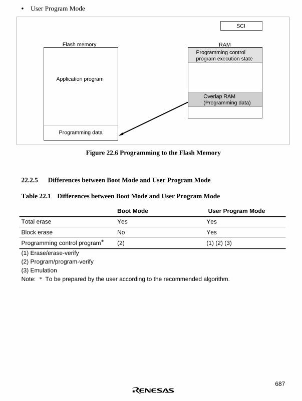
687
• User Program Mode
SCI
RAMFlash memory
Application program
Programming data
Programming control program execution state
Overlap RAM (Programming data)
Figure 22.6 Programming to the Flash Memory
22.2.5 Differences between Boot Mode and User Program Mode
Table 22.1 Differences between Boot Mode and User Program Mode
Boot Mode User Program Mode
Total erase Yes Yes
Block erase No Yes
Programming control program* (2) (1) (2) (3)
(1) Erase/erase-verify(2) Program/program-verify(3) EmulationNote: * To be prepared by the user according to the recommended algorithm.

688
22.2.6 Block Configuration
The flash memory is divided into seven 32 kbyte blocks, one 28 kbyte blocks, and four 1 kbyteblocks.
Address H'00000
Address H'3FFFF
32kbyte
32kbyte
256k
byte
32kbyte
28kbyte
1kbyte1kbyte1kbyte1kbyte
32kbyte
32kbyte
32kbyte
32kbyte
Figure 22.7 Block Configuration

689
22.3 Pin Configuration
The flash memory is controlled by the pins shown in table 22.2.
Table 22.2 Pin Configuration
Pin Name Abbreviation I/O Function
Power-on reset RES Input Power-on reset
Flash write protect FWP Input Flash program/erase protection by hardware
Mode 3 MD3 Input Set operation mode of LSI
Mode 2 MD2 Input Set operation mode of LSI
Mode 1 MD1 Input Set operation mode of LSI
Mode 0 MD0 Input Set operation mode of LSI
Transmit data TxD1 Output Serial send data output
Receive data RxD1 Input Serial receive data input
22.4 Register Configuration
Registers that control the flash memory when the on-chip flash memory is valid are shown in table22.3.
Table 22.3 Register Configuration
NameAbbre-viation R/W Initial Value Address Access Size
Flash memory control register 1 FLMCR1 R/W* 1 H'00* 2 H'FFFF8580 8
Flash memory control register 2 FLMCR2 R/W* 1 H'00* 3 H'FFFF8581 8
Erase block register 1 EBR1 R/W* 1 H'00* 3 H'FFFF8582 8
Erase block register 2 EBR2 R/W* 1 H'00* 3 H'FFFF8583 8
RAM emulation register RAMER R/W H'0000 H'FFFF8628 8, 16, 32
Notes: 1. FLMCR1, FLMCR2, EBR1, and EBR2 are 8-bit registers, and RAMER is a 16-bitregister.
2. Only byte accesses are valid for FLMCR1, FLMCR2, EBR1, and EBR2, the accessrequiring 3 cycles. Three cycles are required for a byte or word access to RAMER, and6 cycles for a longword access.
3. When a longword write is performed on RAMER, 0 must always be written to the lowerword (address H'FFFF8630). Operation is not guaranteed if any other value is written.
* 1 In modes in which the on-chip flash memory is disabled, a read will return H'00, andwrites are invalid. Writes are also disabled when the FWE bit is set to 1 in FLMCR1.
* 2 When a low level is input to the FWP pin, the initial value is H'80.* 3 When a high level is input to the FWP pin, or if a low level is input and the SWE bit in
FLMCR1 is not set, these registers are initialized to H'00.

690
22.5 Description of Registers
22.5.1 Flash Memory Control Register 1 (FLMCR1)
FLMCR1 is an 8-bit register used for flash memory operating mode control. Program-verify modeor erase-verify mode for addresses H'00000–H'1FFFF is entered by setting SWE to 1 when FWE= 1, then setting the EV1 or PV1 bit. Program mode for addresses H'00000–H'1FFFF is entered bysetting SWE to 1 when FWE = 1, then setting the PSU1 bit, and finally setting the P1 bit. Erasemode for addresses H'00000–H'1FFFF is entered by setting SWE to 1 when FWE = 1, then settingthe ESU1 bit, and finally setting the E1 bit. FLMCR1 is initialized in the standby mode or withpower-on reset. Its initial value is H'80 when a low level is input to the FWP pin, and H'00 when ahigh level is input. When on-chip flash memory is disabled, a read will return H'80, and writes areinvalid.
Writes to bits SWE, ESU1, PSU1, EV1, and PV1 are enabled only when FWE = 1 and SWE = 1;writes to the E1 bit only when FWE = 1, SWE = 1, and ESU1 = 1; and writes to the P1 bit onlywhen FWE = 1, SWE = 1, and PSU1 = 1.
Bit: 7 6 5 4 3 2 1 0
FWE SWE ESU1 PSU1 EV1 PV1 E1 P1
Initial value: 0 0 0 0 0 0 0 0
R/W: R R/W R/W R/W R/W R/W R/W R/W
• Bit 7—Flash Write Enable Bit (FWE): Displays the state of the FWP pin which sets hardwareprotection against flash memory programming/erasing.
Bit 7: FWE Description
0 When high level is input to the FWP pin (hardware-protect state)
1 When low level is input to the FWP pin
• Bit 6—Software Write Enable Bit (SWE): Enables or disables the flash memory. This bitshould be set when setting bits 5–0, FLMCR2 bits 5–0, EBR1 bits 3–0, and EBR2 bits 7–0.
Bit 6: SWE Description
0 Writes disabled (Initial value)
1 Writes enabled
[Setting condition] When FWE=1
• Bit 5—Erase Setup Bit 1 (ESU1): Prepares for a transition to erase mode (applicableaddresses: H'00000–H'1FFFF). Do not set the SWE, PSU1, EV1, PV1, E1, or P1 bit at thesame time.

691
Bit 5: ESU1 Description
0 Erase setup release (Initial value)
1 Erase setup
[Setting condition] When FWE=1 and SWE=1
• Bit 4—Program Setup Bit 1 (PSU1): Prepares for a transition to program mode (applicableaddresses: H'00000–H'1FFFFF). Do not set the SWE, ESU1, EV1, PV1, E1, or P1 bit at thesame time.
Bit 4: PSU1 Description
0 Program setup release (Initial value)
1 Program setup
[Setting condition] When FWE=1 and SWE=1
• Bit 3—Erase-Verify 1 (EV1): Selects erase-verify mode transition or release (applicableaddresses: H'00000–H'1FFFF). Do not set the SWE, ESU1, PSU1, PV1, E1, or P1 bit at thesame time.
Bit 3: EV1 Description
0 Erase verify mode release (Initial value)
1 Transition to erase verify mode
[Setting condition] When FWE=1 and SWE=1
• Bit 2—Program-Verify 1 (PV1): Selects program-verify mode transition or release (applicableaddresses: H'00000–H'1FFFF). Do not set the SWE, ESU1, PSU1, EV1, E1, or P1 bit at thesame time.
Bit 2: PV1 Description
0 Program verify mode release (Initial value)
1 Transition to program verify mode
[Setting condition] When FWE=1 and SWE=1

692
• Bit 1—Erase 1 (E1): Selects erase mode transition or release (applicable addresses: H'00000–H'1FFFF). Do not set the SWE, ESU1, PSU1, EV1, PV1, or P1 bit at the same time.
Bit 1: E1 Description
0 Erase mode release (Initial value)
1 Transition to erase mode
[Setting condition] When FWE=1, SWE=1, and ESU1=1
• Bit 0—Program 1 (P1): Selects program mode transition or release (applicable addresses:H'00000–H'1FFFF). Do not set the SWE, PSU1, ESU1, EV1, PV1, or E1 bit at the same time.
Bit 0: P1 Description
0 Program setup mode release (Initial value)
1 Program setup
[Setting condition] When FWE=1, SWE=1, and PSU1=1
22.5.2 Flash Memory Control Register 2 (FLMCR2)
FLMCR2 is an 8-bit register used for flash memory operating mode control. Program-verify modeor erase-verify mode for addresses H'20000–H'3FFFF is entered by setting SWE (FLMCR1) to 1when FWE (FLMCR1) = 1, then setting the EV2 or PV2 bit. Program mode for addressesH'20000–H'3FFFF is entered by setting SWE (FLMCR1) to 1 when FWE (FLMCR1) = 1, thensetting the PSU2 bit, and finally setting the P2 bit. Erase mode for addresses H'20000–H'3FFFF isentered by setting SWE (FLMCR1) to 1 when FWE (FLMCR1) = 1, then setting the ESU2 bit,and finally setting the E2 bit. FLMCR2 is initialized to H'00 by a power-on reset, in standbymode, when a high level is input to the FWP pin, and when a low level is input to the FWP pinand the SWE bit in FLMCR1 is not set (the exception is the FLER bit, which is initialized only bya power-on reset). When on-chip flash memory is disabled, a read will return H'00, and writes areinvalid.
Writes to bits ESU2, PSU2, EV2, and PV2 in FLMCR2 are enabled only when FWE (FLMCR1) =1 and SWE (FLMCR1) = 1; writes to the E2 bit only when FWE (FLMCR1) = 1, SWE(FLMCR1) = 1, and ESU2 = 1; and writes to the P2 bit only when FWE (FLMCR1) = 1, SWE(FLMCR1) = 1, and PSU2 = 1.

693
Bit: 7 6 5 4 3 2 1 0
FLER — ESU2 PSU2 EV2 PV2 E2 P2
Initial value: 0 0 0 0 0 0 0 0
R/W: R R R/W R/W R/W R/W R/W R/W
• Bit 7—Flash Memory Error (FLER): Indicates that an error has occurred during an operationon flash memory (programming or erasing). When FLER is set to 1, flash memory goes to theerror-protection state.
Bit 7: FLER Description
0 Flash memory is operating normally. (Initial value)
Flash memory program/erase protect (error protect) disabled
1 Indicates error during flash memory program/erase.
Flash memory program/erase protect (error protect) enabled
[Setting condition] See section 22.8.3, Error protection
• Bit 6—Reserved bit: This bit is always read as 0.
• Bit 5—Erase Setup Bit 2 (ESU2): Prepares for a transition to erase mode (applicableaddresses: H'20000–H'3FFFF). Do not set the PSU2, EV2, PV2, E2, or P2 bit at the same time.
Bit 5: ESU2 Description
0 Erase setup release (Initial value)
1 Erase setup
[Setting condition] When FWE=1 and SWE=1
• Bit 4—Program Setup Bit 2 (PSU2): Prepares for a transition to program mode (applicableaddresses: H'20000–H'3FFFF). Do not set the ESU2, EV2, PV2, E2, or P2 bit at the same time.
Bit 4: PSU2 Description
0 Program setup release (Initial value)
1 Program setup
[Setting condition] When FWE=1 and SWE=1

694
• Bit 3—Erase-Verify 2 (EV2): Selects erase-verify mode transition or release (applicableaddresses: H'20000–H'3FFFF). Do not set the ESU2, PSU2, PV2, E2, or P2 bit at the sametime.
Bit 3: EV2 Description
0 Erase verify mode release (Initial value)
1 Transition to the erase verify mode
[Setting condition] When FWE=1 and SWE=1
• Bit 2—Program-Verify 2 (PV2): Selects program-verify mode transition or release (applicableaddresses: H'20000–H'3FFFF). Do not set the ESU2, PSU2, EV2, E2, or P2 bit at the sametime.
Bit 2: PV2 Description
0 Program verify mode release (Initial value)
1 Transition to the program verify mode
[Setting condition] When FWE=1, and SWE=1
• Bit 1—Erase 2 (E2): Selects erase mode transition or release (applicable addresses: H'20000–H'3FFFF). Do not set the ESU2, PSU2, EV2, PV2, or P2 bit at the same time.
Bit 1: E2 Description
0 Erase mode release (Initial value)
1 Transition to the erase mode
[Setting condition] When FWE=1, SWE=1, and ESU2=1
• Bit 0—Program 2 (P2): Selects program mode transition or release (applicable addresses:H'20000–H'3FFFF). Do not set the ESU2, PSU2, EV2, PV2, or E2 bit at the same time.
Bit 0: P2 Description
0 Program mode release(Initial value)
1 Transition to the program mode
[Setting condition] When FWE=1, SWE=1, and PSU2=1

695
22.5.3 Erase Block Register 1 (EBR1)
EBR1 is an 8-bit register that specifies the flash memory erase area block by block. EBR1 isinitialized to H'00 by a power-on reset and standby mode, when a high level is input to the FWPpin, and when a low level is input to the FWP pin and the SWE bit in FLMCR1 is not set. When abit in EBR1 is set to 1, the corresponding block can be erased. Other blocks are erase-protected.Only one of the bits of EBR1 and EBR2 combined can be set. Do not set more than one bit. Ifmore than one bit is set, writes to bits ESU1, ESU2, E1, and E2 will be invalid. When on-chipflash memory is disabled, a read will return H'00, and writes are invalid.
The flash memory block configuration is shown in table 22.4.
Bit: 7 6 5 4 3 2 1 0
— — — — EB3 EB2 EB1 EB0
Initial value: 0 0 0 0 0 0 0 0
R/W: R R R R R/W R/W R/W R/W
22.5.4 Erase Block Register 2 (EBR2)
EBR2 is an 8-bit register that specifies the flash memory erase area block by block. EBR2 isinitialized to H'00 by a power-on reset and standby mode, when a high level is input to the FWPpin, and when a low level is input to the FWP pin and the SWE bit in FLMCR1 is not set. When abit in EBR2 is set to 1, the corresponding block can be erased. Other blocks are erase-protected.When on-chip flash memory is disabled, a read will return H'00, and writes are invalid.
The flash memory block configuration is shown in table 22.4.
Bit: 7 6 5 4 3 2 1 0
EB11 EB10 EB9 EB8 EB7 EB6 EB5 EB4
Initial value: 0 0 0 0 0 0 0 0
R/W: R/W R/W R/W R/W R/W R/W R/W R/W
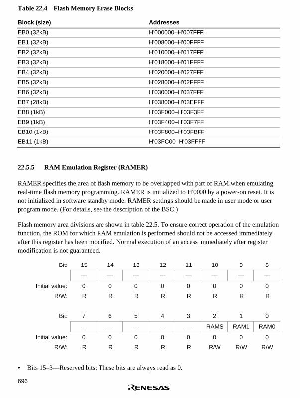
696
Table 22.4 Flash Memory Erase Blocks
Block (size) Addresses
EB0 (32kB) H'000000–H'007FFF
EB1 (32kB) H'008000–H'00FFFF
EB2 (32kB) H'010000–H'017FFF
EB3 (32kB) H'018000–H'01FFFF
EB4 (32kB) H'020000–H'027FFF
EB5 (32kB) H'028000–H'02FFFF
EB6 (32kB) H'030000–H'037FFF
EB7 (28kB) H'038000–H'03EFFF
EB8 (1kB) H'03F000–H'03F3FF
EB9 (1kB) H'03F400–H'03F7FF
EB10 (1kB) H'03F800–H'03FBFF
EB11 (1kB) H'03FC00–H'03FFFF
22.5.5 RAM Emulation Register (RAMER)
RAMER specifies the area of flash memory to be overlapped with part of RAM when emulatingreal-time flash memory programming. RAMER is initialized to H'0000 by a power-on reset. It isnot initialized in software standby mode. RAMER settings should be made in user mode or userprogram mode. (For details, see the description of the BSC.)
Flash memory area divisions are shown in table 22.5. To ensure correct operation of the emulationfunction, the ROM for which RAM emulation is performed should not be accessed immediatelyafter this register has been modified. Normal execution of an access immediately after registermodification is not guaranteed.
Bit: 15 14 13 12 11 10 9 8
— — — — — — — —
Initial value: 0 0 0 0 0 0 0 0
R/W: R R R R R R R R
Bit: 7 6 5 4 3 2 1 0
— — — — — RAMS RAM1 RAM0
Initial value: 0 0 0 0 0 0 0 0
R/W: R R R R R R/W R/W R/W
• Bits 15–3—Reserved bits: These bits are always read as 0.

697
• Bit 2—RAM Select (RAMS): Specifies selection or non-selection of flash memory emulationin RAM. When RAMS = 1, all flash memory block are program/erase-protected. This bit isignored when the on-chip ROM is disabled.
Bit 2: RAMS Description
0 Emulation not selected
Program/erase protect of all flash memory blocks is disabled (Initial value)
1 Emulation selected
Program/erase protect of all flash memory blocks is enabled
• Bits 1 and 0—Flash Memory Area Selection (RAM1, RAM0): These bits are used togetherwith bit 2 to select the flash memory area to be overlapped with RAM. (See table 22.5.)
Table 22.5 Separation of the Flash Memory Area
Addresses Block Name RAMS RAM1 RAM0
H'FFF800–H'FFFBFF RAM area 1kB 0 * *
H'03F000–H'03F3FF EB8 (1kB) 1 0 0
H'03F400–H'03F7FF EB9 (1kB) 1 0 1
H'03F800–H'03FBFF EB10(1kB) 1 1 0
H'03FC00–H'03FFFF EB11(1kB) 1 1 1

698
22.6 On-Board Programming Mode
When pins are set to on-board programming mode and a power-on reset is executed, a transition ismade to the on-board programming state in which program/erase/verify operations can beperformed on the on-chip flash memory. There are two on-board programming modes: boot modeand user program mode. The pin settings for transition to each of these modes are shown in table22.6. For a diagram of the transitions to the various flash memory modes, see figure 22.2.
Table 22.6 Setting On-Board Programming Modes
Mode PLL Multiple FWP MD3 MD2 MD1 MD0
Boot mode Expanded Mode ×1 0 0 0 0 0
Single-chip Mode 0 0 0 1
Expanded Mode ×2 0 1 0 0
Single-chip Mode 0 1 0 1
Expanded Mode ×4 1 0 0 0
Single-chip Mode 1 0 0 1
User program mode Expanded Mode ×1 0 0 0 1 0
Single-chip Mode 0 0 1 1
Expanded Mode ×2 0 1 1 0
Single-chip Mode 0 1 1 1
Expanded Mode ×4 1 0 1 0
Single-chip Mode 1 0 1 1

699
22.6.1 Boot Mode
When boot mode is used, the flash memory programming control program must be prepared in thehost beforehand. The SCI to be used is set to channel asynchronous mode.
When a reset start is executed after the LSI pins have been set to boot mode in the power-on resetstate, the boot program built into the LSI is started and the programming control program preparedin the host is serially transmitted to the LSI via SCI channel 1. In the LSI, the programmingcontrol program received via SCI channel 1 is written into the programming control program areain on-chip RAM. After the transfer is completed, control branches to the start address of theprogramming control program area and the programming control program execution state isentered (flash memory programming is performed).
The transferred programming control program must therefore include coding that follows theprogramming algorithm given later.
The system configuration in boot mode is shown in figure 22.8, and the boot mode executionprocedure in figure 22.9.
RXD1
TXD1SCI1
Host Write data reception
Verify data transmission
LSI
Flash memory
On-chip RAM
Figure 22.8 System Configuration in Boot Mode

700
n=1
n=N?
n+1→n
Yes
No
Note: If a memory cell does not operate normally and cannot be erased, one H'FF byte is transmitted as an erase error, and the erase operation and subsequent operations are halted.
Start
Set pin to the boot program mode then reset start
The host continuously sends data (H'00) using a fixed bit rate
This LSI measures the low period of data H'00 sent by the host
This LSI calculates the bit rate and sets value to the bit rate register
After adjustment of the bit rate, this LSI sends 1 byte of data H'00 to the host as a sign of completion of adjustment
The host checks whether the sign (H'00) indicating completion of bit rate adjustment is received, then transmits 1 byte of data H'55
After receiving H'55, this LSI sends 1 byte of H'AA
The host sends the byte number (N) of the user program in sequence of upper byte then lower byte
This LSI sends the received byte number to the host as verify data (echo back)
The host transmits the user program in sequence using byte units
This LSI sends the received program to the host as verify data (echo back)
The received user program is transferred to the on-chip RAM
Transmission complete
Data of the flash memory is checked. All data are erased if data already exists
After confirming that all data of the flash memory have been erased, this LSI sends 1 byte of H'AA to the host
The write control program transferred to the on-chip RAM is executed
Figure 22.9 Boot Mode Execution Procedure

701
Automatic SCI Bit Rate Adjustment
StartBit
StopBit
D0 D1 D2 D3 D4 D5 D6 D7
High period of more than 1 bit
Low period (9 bits) measured (H'00 data)
Figure 22.10 Automatic SCI Bit Rate Adjustment
When boot mode is initiated, the LSI measures the low period of the asynchronous SCIcommunication data (H'00) transmitted continuously from the host. The SCI transmit/receiveformat should be set as follows: 8-bit data, 1 stop bit, no parity. The LSI calculates the bit rate ofthe transmission from the host from the measured low period, and transmits one H'00 byte to thehost to indicate the end of bit rate adjustment. The host should confirm that this adjustment endindication (H'00) has been received normally, and transmit one H'55 byte to the LSI. If receptioncannot be performed normally, initiate boot mode again (reset), and repeat the above operations.Depending on the host’s transmission bit rate and the LSI’s system clock frequency, there will bea discrepancy between the bit rates of the host and the LSI. To ensure correct SCI operation, thehost's transfer bit rate should be set to 9,600 or 4,800 bps.
Table 22.7 shows host transfer bit rates and system clock frequencies for which automaticadjustment of the LSI bit rate is possible. The boot program should be executed within this systemclock range.
Table 22.7 System Clock Frequencies for which Automatic Adjustment of LSI Bit Rate isPossible
Host Bit RateSystem Clock Frequency for which Automatic Adjustmentof LSI Bit Rate is Possible
9,600 bps 8 to 28.7 MHz
4,800 bps 4 to 20 MHz

702
On-Chip RAM Area Divisions in Boot Mode: In boot mode, the RAM area is divided into anarea used by the boot program and an area to which the programming control program istransferred via the SCI, as shown in figure 22.11. The boot program area cannot be used until theexecution state in boot mode switches to the programming control program transferred from thehost.
Boot program area (2k bytes)
Programming control program area (2k bytes)
H'FFFFF000
H'FFFFF800
H'FFFFFFFF
Figure 22.11 RAM Areas in Boot Mode
Note: The boot program area cannot be used until a transition is made to the execution state forthe programming control program transferred to RAM. Note also that the boot programremains in this area of the on-chip RAM even after control branches to the programmingcontrol program.

703
22.6.2 User Program Mode
After setting FWP, the user should branch to, and execute, the previously preparedprogramming/erase control program.
As the flash memory itself cannot be read while flash memory programming/erasing is beingexecuted, the control program that performs programming and erasing should be run in on-chipRAM or external memory.
Use the following procedure (figure 22.12) to execute the programming control program thatwrites to flash memory (when transferred to RAM).
Execute user applicationprogram
Execute programming/erase control program in RAM
(flash memory rewriting)
Transfer programming/erasecontrol program to RAM
FWP = 1 (user program mode)
Write FWP assessment programand transfer program1
2
3
4
5
Figure 22.12 User Program Mode Execution Procedure
Notes: 1. When programming and erasing, start the watchdog timer so that measures can betaken to prevent program runaway, etc. Memory cells may not operate normally ifoverprogrammed or overerased due to program runaway.
2. If an address at which a flash memory register resides is read in the mask ROM orZTAT version, the value will be undefined. When a flash memory version program isused in the mask ROM or ZTAT version, the state of the FWP pin cannot bedetermined. A modification must therefore be made to prevent operation of the flashmemory rewrite program.

704
22.7 Programming/Erasing Flash Memory
A software method, using the CPU, is employed to program and erase flash memory in the on-board programming modes. There are four flash memory operating modes: program mode, erasemode, program-verify mode, and erase-verify mode. Transitions to these modes are made bysetting the PSU1, ESU1, P1, E1, PV1, and EV1 bits in FLMCR1 for addresses H'00000–H'1FFFF,or the PSU2, ESU2, P2, E2, PV2, and EV2 bits in FLMCR2 for addresses H'20000–H'3FFFF.
The flash memory cannot be read while being programmed or erased. Therefore, the program(programming control program) that controls flash memory programming/erasing should belocated and executed in on-chip RAM or external memory.
Notes: 1. Operation is not guaranteed if setting/resetting of the SWE, ESU1, PSU1, EV1, PV1,E1, and P1 bits in FLMCR1, or the ESU2, PSU2, EV2, PV2, E2, and P2 bits inFLMCR2, is executed by a program in flash memory.
2. When programming or erasing, set FWP to low level (programming/erasing will not beexecuted if FWP is set to high level).
3. Programming should be performed in the erased state. Do not perform additionalprogramming on previously programmed addresses.
4. Do not program addresses H'00000–H'1FFFF and H'20000–H'3FFFF simultaneously.Operation is not guaranteed if this is done.
22.7.1 Program Mode (n = 1 for Addresses H'0000–H'1FFFF, n = 2 for Addresses
H'20000–H'3FFFF)
When writing data or programs to flash memory, the program/program-verify flowchart shown infigure 22.13 should be followed. Performing program operations according to this flowchart willenable data or programs to be written to flash memory without subjecting the device to voltagestress or sacrificing program data reliability. Programming should be carried out 32 bytes at atime.
Following the elapse of 10 µs or more after the SWE bit is set to 1 in flash memory controlregister 1 (FLMCR1), 32-byte program data is stored in the program data area and reprogram dataarea, and the 32-byte data in the program data area in RAM is written consecutively to theprogram address (the lower 8 bits of the first address written to must be H'00, H'20, H'40, H'60,H'80, H'A0, H'C0, or H'E0). Thirty-two consecutive byte data transfers are performed. Theprogram address and program data are latched in the flash memory. A 32-byte data transfer mustbe performed even if writing fewer than 32 bytes; in this case, H'FF data must be written to theextra addresses.
Next, the watchdog timer is set to prevent overprogramming in the event of program runaway, etc.Set a minimum value of 300 µs or more as the WDT overflow period. After this, preparation forprogram mode (program setup) is carried out by setting the PSUn bit in FLMCRn, and after theelapse of 50 µs or more, the operating mode is switched to program mode by setting the Pn bit in

705
FLMCRn. The time during which the Pn bit is set is the flash memory programming time. Set200 µs as the time for one programming operation.
22.7.2 Program-Verify Mode (n = 1 for Addresses H'0000–H'1FFFF, n = 2 for Addresses
H'20000–H'3FFFF)
In program-verify mode, the data written in program mode is read to check whether it has beencorrectly written in the flash memory.
After the elapse of a given programming time, the programming mode is exited (the Pn bit inFLMCRn is released, then the PSUn bit is released at least 10 µs later). The watchdog timer isreleased after the elapse of 10 µs or more, and the operating mode is switched to program-verifymode by setting the PVn bit in FLMCRn. Before reading in program-verify mode, a dummy writeof H'FF data should be made to the addresses to be read. The dummy write should be executedafter the elapse of 4 µs or more. When the flash memory is read in this state (verify data is read in32-bit units), the data at the latched address is read. Wait at least 2 µs after the dummy writebefore performing this read operation. Next, the written data is compared with the verify data, andreprogram data is computed (see figure 22.13) and transferred to the reprogram data area. After 32bytes of data have been verified, exit program-verify mode, wait for at least 4 µs, then release theSWE bit in FLMCR1. If reprogramming is necessary, set program mode again, and repeat theprogram/program-verify sequence as before. However, ensure that the program/program-verifysequence is not repeated more than 1,000 times on the same bits.

706
Set SWE bit in FLMCR1
n = 1
m = 0
Write 32-byte data in reprogram data area in RAM to flash memory consecutively
Start of programming
NG
NG
NG NG
OK
OK
OK
*2
*5
*5
*5
*5
*5
*5
*5
*5
*5
Store 32-byte program data inreprogram data area
*4
*1
*5
Read verify data
Clear SWE bit in FLMCR1
m = 1
End of programming
Program data = verify data?
End of 32-bytedata verification?
flag = 0?
VerifyIncrement address
Programming failure
OK
Clear SWE bit in FLMCR1
n ≥ 1000
n ← n + 1
Notes: *1 Data transfer is performed by byte transfer. The lower 8 bits of the first address written to must be H'00, H'20, H'40, H'60, H'80, H'A0, H'C0, or H'E0. A 32-byte data transfer must be performed even if writing fewer than 32 bytes; in this case, H'FF data must be written to the extra addresses.*2 Verify data is read in 32-bit (longword) units.*3 Even bits for which programming has been completed in a 32-byte programming loop will be subjected to additional programming if they fail the subsequent verify operation.*4 A 32-byte area for storing program data and a 32-byte area for storing reprogram data are required in RAM. The contents of the latter are rewritten according to the progress of the programming operation.*5 Make sure to set the wait times and repetitions as specified. Programming may not complete correctly if values other than the specified ones are used.
Start
RAM
Program data storagearea (32 bytes)
Reprogram data storage area (32 bytes)
*3
*3
*4
End of programming
Perform programming in the erased state. Do not perform additional programming on previously programmed addresses.
Write data (D)
Note: The memory erased state is 1. Programming is performed on 0 data.
Verify data (V) Rewrite data (X) Comment
Programming completed
Programming incomplete; reprogram
Still in erased state; no action
0011
0101
1011
Enable WDT
Disable WDT
Reprogram data computation
Transfer reprogram data to reprogram data area
Wait 10 µs
Clear PV1(2) bit in FLMCR1(2)
Wait 4 µs
Dummy write of H'FF to verify address
Wait 2 µs
Set PV1(2) bit in FLMCR1(2)
Wait 4 µs
Clear PSU1(2) bit in FLMCR1(2)
Wait 10 µs
Clear P1(2) bit in FLMCR1(2)
Wait 10 µs
Set P1(2) bit in FLMCR1(2)
Wait 200 µs
Set PSU1(2) bit in FLMCR1(2)
Wait 50 µs
Figure 22.13 Program/Program Verify Flow

707
• Sample 32-byte programming program
The wait time set values (number of loops) are for the case where f = 28.7 MHz. For otherfrequencies, the set value is given by the following expression:
Wait time (µs) × f (MHz) ÷ 4
Registers Used
R4 (input): Program data storage addressR5 (input): Programming destination addressR7 (output): OK (normal) or NG (error)R0-3, 8-13: Work registers
FLMCR1 .EQU H’80
FLMCR2 .EQU H’81
OK .EQU H’0
NG .EQU H’1
Wait10u .EQU 72
Wait50u .EQU 359
Wait4u .EQU 29
Wait2u .EQU 14
Wait200u .EQU 1435
WDT_TCSR .EQU H’FFFF8610
WDT_573u .EQU H’A579
SWESET .EQU B’01000000
PSU1SET .EQU B’00010000
P1SET .EQU B’00000001
P1CLEAR .EQU B’11111110
PSU1CLEAR .EQU B’11101111
PVSET .EQU B’00000100
PVCLEAR .EQU B’11111011
SWECLEAR .EQU B’10111111
MAXVerify .EQU 1000
;
FlashProgram .EQU $
MOV #H’01,R2 ; R2 work register (1)
MOV.L #PdataBuff,R0 ; Save program data to work area
MOV R4,R12
MOV #8,R13
COPY_LOOP .EQU $

708
MOV.L @R12+,R1
MOV.L R1,@R0
ADD.L #4,R0
ADD.L #-1,R13
CMP/PL R13
BT COPY_LOOP
MOV.L #H’FFFF8500,R0 ; Initialize GBR
LDC R0,GBR
;
MOV.L #Wait10u,R3
MOV.L #FLMCR1,R0 ; Initialize R0 to FLCMR1 address
OR.B #SWESET,@(R0,GBR) ; Set SWE
Wait_1 SUBC R2,R3 ; Wait 10 µs
BF Wait_1
;
MOV.L #H’20000,R9
CMP/GT R5,R9
BT Program_Start
MOV.L #FLMCR2,R0
Program_Start .EQU $
MOV.L #0,R9 ; Initialize n (R9) to 0
;
Program_loop .EQU $
MOV.L #0,R10 ; Initialize m (R10) to 0
MOV.L #32,R3 ; Write 32-byte data consecutively
MOV.L #PdataBuff,R12
MOV.L R5,R13
Write_Loop .EQU $
MOV.B @R12+,R1
MOV.B R1,@R13
ADD.L #1,R13
ADD.L #-1,R3
CMP/PL R3
BT Write_Loop
;
MOV.L #WDT_TCSR,R1 ; Enable WDT
MOV.W #WDT_573u,R3 ; 573.4 µs cycle

709
MOV.W R3,@R1
;
MOV.L #Wait50u,R3
OR.B #PSU1SET,@(R0,GBR) ; Set PSU
Wait_2 SUBC R2,R3 ; Wait 50 µs
BF
;
MOV.L #Wait200u,R3
OR.B #P1SET,@(R0,GBR) ; Set P
Wait_3 SUBC R2,R3 ; Wait 200 µs
BF Wait_3
;
MOV.L #Wait10u,R3
AND.B #P1CLEAR,@(R0,GBR) ; Clear P
Wait_4 SUBC R2,R3 ; Wait 10 µs
BF Wait_4
;
MOV.L #Wait10u,R3
AND.B #PSU1CLEAR,@(R0,GBR) ; Clear PSU
Wait_5 SUBC R2,R3 ; Wait 10 µs
BF Wait_5
;
MOV.L #WDT_TCSR,R1 ; Disable WDT
MOV.W #H’A55F,R3
MOV.W R3,@R1
;
MOV.L #Wait4u,R3
OR.B #PVSET,@(R0,GBR) ; Set PV
Wait_6 SUBC R2,R3 ; Wait 4 µs
BF Wait_6
;
MOV.L PdataBuff,R3
MOV.L R4,R1
MOV.L R5,R12
MOV.L #8,R13
MOV.L #H’FFFFFFFF,R11
;
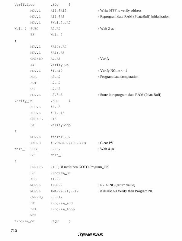
710
VerifyLoop .EQU $
MOV.L R11,@R12 ; Write H'FF to verify address
MOV.L R11,@R3 ; Reprogram data RAM (PdataBuff) initialization
MOV.L #Wait2u,R7
Wait_7 SUBC R2,R7 ; Wait 2 µs
BF Wait_7
;
MOV.L @R12+,R7
MOV.L @R1+,R8
CMP/EQ R7,R8 ; Verify
BT Verify_OK
MOV.L #1,R10 ; Verify NG, m <- 1
XOR R8,R7 ; Program data computation
NOT R7,R7
OR R7,R8
MOV.L R8,@R3 ; Store in reprogram data RAM (PdataBuff)
Verify_OK .EQU $
ADD.L #4,R3
ADD.L #-1,R13
CMP/PL R13
BT VerifyLoop
;
MOV.L #Wait4u,R7
AND.B #PVCLEAR,@(R0,GBR) ; Clear PV
Wait_8 SUBC R2,R7 ; Wait 4 µs
BF Wait_8
;
CMP/PL R10 ; if m=0 then GOTO Program_OK
BF Program_OK
ADD #1,R9
MOV.L #NG,R7 ; R7 <- NG (return value)
MOV.L #MAXVerify,R12 ; if n>=MAXVerify then Program NG
CMP/EQ R9,R12
BT Program_end
BRA Program_loop
NOP
Program_OK .EQU $

711
MOV.L #OK,R7 ; R7 <- OK (return value)
Program_end .EQU $
MOV.B #H’00,R0
MOV.B R0,@(FLMCR1,GBR) ; Clear SWE
;
RTS
NOP
;
.ALIGN 4
PdataBuff .RES.B 32
22.7.3 Erase Mode (n = 1 for Addresses H'0000–H'1FFFF, n = 2 for Addresses H'20000–
H'3FFFF)
When erasing flash memory, the erase/erase-verify flowchart shown in figure 22.14 should befollowed.
To perform data or program erasure, set the flash memory area to be erased in erase block registern (EBRn) at least 10 µs after setting the SWE bit to 1 in flash memory control register 1(FLMCR1). Next, the watchdog timer is set to prevent overerasing in the event of programrunaway, etc. Set 5.3 µs as the WDT overflow period. After this, preparation for erase mode (erasesetup) is carried out by setting the ESUn bit in FLMCRn, and after the elapse of 200 µs or more,the operating mode is switched to erase mode by setting the En bit in FLMCRn. The time duringwhich the En bit is set is the flash memory erase time. Set an erase time of 5 ms.
Note: With flash memory erasing, preprogramming (setting all memory data in the memory tobe erased to all “0”) is not necessary before starting the erase procedure.

712
22.7.4 Erase-Verify Mode (n = 1 for Addresses H'00000–H'1FFFF, n = 2 for Addresses
H'20000–H'3FFFF)
In erase-verify mode, data is read after memory has been erased to check whether it has beencorrectly erased.
After the elapse of the erase time, erase mode is exited (the En bit in FLMCRn is released, thenthe ESUn bit is released at least 10 µs later), the watchdog timer is released after the elapse of 10µs or more, and the operating mode is switched to erase-verify mode by setting the EVn bit inFLMCRn. Before reading in erase-verify mode, a dummy write of H'FF data should be made tothe addresses to be read. The dummy write should be executed after the elapse of 20 µs or more.When the flash memory is read in this state (verify data is read in 32-bit units), the data at thelatched address is read. Wait at least 2 µs after the dummy write before performing this readoperation. If the read data has been erased (all “1”), a dummy write is performed to the nextaddress, and erase-verify is performed. If the read data is unerased, set erase mode again andrepeat the erase/erase-verify sequence in the same way. However, ensure that the erase/erase-verify sequence is not repeated more than 60 times. When verification is completed, exit erase-verify mode, and wait for at least 5 µs. If erasure has been completed on all the erase blocks aftercompleting erase-verify operations on all these blocks, release the SWE bit in FLMCR1. If thereare any unerased blocks, set erase mode again, and repeat the erase/erase-verify sequence asbefore. However, ensure that the erase/erase-verify sequence is not repeated more than 60 times.

713
End of erasing
Start
Set SWE bit in FLMCR1
Set ESU1(2) bit in FLMCR1(2)
Set E1(2) bit in FLMCR1(2)
Wait 10 µs
Wait 200 µs
n = 1
Set EBR1(2)
Enable WDT
*3
*5
*5
*5
*5
*5
*5
*5 *5
*5
*5
Wait 5 ms
Wait 10 µs
Wait 10 µs
Wait 20 µs
Set block start address to verify address
Wait 2 µs
Wait 5 µs
*2
*4
Start erase
Clear E1(2) bit in FLMCR1(2)
Clear ESU1(2) bit in FLMCR1(2)
Set EV1(2) bit in FLMCR1(2)
H'FF dummy write to verify address
Read verify data
Clear EV1(2) bit in FLMCR1(2)
Wait 5 µs
Clear EV1(2) bit in FLMCR1(2)
Clear SWE bit in FLMCR1
Disable WDT
Halt erase
*1
Verify data = all "1"?
Last address of block?
End oferasing of all erase
blocks?
Erase failure
Clear SWE bit in FLMCR1
n ≥ 60?
NG
NG
NG NG
OK
OK
OK OK
n ← n + 1
Incrementaddress
Notes: *1 Preprogramming (setting erase block data to all “0”) is not necessary.*2 Verify data is read in 32-bit (longword) units.*3 Set only one bit in EBR1(2). More than one bit cannot be set.*4 Erasing is performed in block units. To erase a number of blocks, each block must be erased in turn.*5 Make sure to set the wait times and repetitions as specified. Erasing may not complete correctly if values other
than the specified ones are used.
Figure 22.14 Erase/Erase-Verify Flowchart (Single Block Erase)

714
• Sample one-block erase program
The wait time set values (number of loops) are for the case where f = 28.7 MHz. For otherfrequencies, the set value is given by the following expression:
Wait time (µS) × f (MHz) ÷ 4
The WDT overflow cycle set value is for the case where f = 28.7 MHz. For other frequencies,ensure that the overflow cycle is a minimum of 5.3 ms.
Registers Used
R5 (input): Memory block table pointerR7 (output): OK (normal) or NG (error)R0-3, 6, 8-9: Work registers
FLMCR1 .EQU H’80
FLMCR2 .EQU H’81
EBR1 .EQU H’82
EBR2 .EQU H’83
Wait10u .EQU 72
Wait2u .EQU 14
Wait200u .EQU 1435
Wait5m .EQU 35875
Wait20u .EQU 144
Wait5u .EQU 36
WDT_TCSR .EQU H’FFFF8610
WDT_9m .EQU H’A57D
SWESET .EQU B’01000000
ESUSET .EQU B’00100000
ESET .EQU B’00000010
ECLEAR .EQU B’11111101
ESUCLEAR .EQU B’11011111
EVSET .EQU B’00001000
EVCLEAR .EQU B’11110111
SWECLEAR .EQU B’10111111
MAXErase .EQU 60
;
FlashErase .EQU $
MOV.L #H’FFFF8500,R0
LDC R0,GBR ; Initialize GBR
MOV.L #1,R2

715
;
MOV.L #Wait10u,R3
MOV.L #FLMCR1,R0
OR.B #SWESET,@(R0,GBR) ; Set SWE
EWait_1 SUBC R2,R3 ; Wait 10 µs
BF EWait_1
;
MOV.L #0,R9 ; Initialize n (R9) to 0
;
MOV.B @(6,R5),R0
MOV.B R0,@(EBR1,GBR) ; Erase memory block (EBR1) setting
MOV.B @(7,R5),R0
MOV.B R0,@(EBR2,GBR) ; Erase memory block (EBR2) setting
;
MOV.L #FLMCR1,R0
MOV.L @R5,R6 ; Erase memory block start address -> R6
MOV.L #H’020000,R7
CMP/GT R6,R7
BT EraseLoop
MOV.L #FLMCR2,R0
;
EraseLoop .EQU $
MOV.L #WDT_TCSR,R1 ; Enable WDT
MOV.W #WDT_9m,R3 ; 9.2 ms cycle
MOV.W R3,@R1
;
MOV.L #Wait200u,R3
OR.B #ESUSET,@(R0,GBR) ; Set ESU
EWait_2 SUBC R2,R3 ; Wait 200 µs
BF EWait_2
;
MOV.L #Wait5m,R3
OR.B #ESET,@(R0,GBR) ; Set E
EWait_3 SUBC R2,R3 ; Wait 5 ms
BF EWait_3
;
MOV.L #Wait10u,R3

716
AND.B #ECLEAR,@(R0,GBR) ; Clear E
EWait_4 SUBC R2,R3 ; Wait 10 µs
BF EWait_4
;
MOV.L #Wait10u,R3
AND.B #ESUCLEAR,@(R0,GBR) ; Clear ESU
EWait_5 SUBC R2,R3 ; Wait 10 µs
BF EWait_5
;
MOV.L #WDT_TCSR,R1 ; Disable WDT
MOV.W #H’A55F,R3
MOV.W R3,@R1
;
MOV.L #Wait20u,R3
OR.B #EVSET,@(R0,GBR) ; Set EV
EWait_6 SUBC R2,R3 ; Wait 20 µs
BF EWait_6
;
MOV.L @R5,R6 ; Erase memory block start address -> R6
BlockVerify_1 .EQU $ ; Erase-verify
MOV.L #H’FFFFFFFF,R8
MOV.L R8,@R6 ; H'FF dummy write
MOV.L #Wait2u,R3
EWait_7 SUBC R2,R3
BF EWait_7
;
MOV.L @R6+,R1 ; Read verify data
CMP/EQ R8,R1
BF BlockVerify_NG
MOV.L @(8,R5),R7
CMP/EQ R6,R7 ; Check for last address of memory block
BF BlockVerify_1
MOV.L #Wait5u,R3
AND.B #EVCLEAR,@(R0,GBR) ; Clear EV
EWait_8 SUBC R2,R3 ; Wait 5 µs
BF EWait_8
;

717
MOV.L #OK,R7 ; R7 <- OK (return value)
BRA FlashErase_end ; Verify OK
NOP
;
BlockVerify_NG .EQU $
ADD.L #1,R9 ; Verify NG, n <- n + 1
MOV.L #Wait5u,R3
AND.B #EVCLEAR,@(R0,GBR) ; Clear EV
EWait_9 SUBC R2,R3 ; Wait 5 µs
BF EWait_9
MOV.L #MAXErase,R7 ; If n > MAXErase then erase NG
CMP/EQ R7,R9
BF EraseLoop
MOV.L #NG,R7 ; R7 <- NG (return value)
FlashErase_end .EQU $
MOV.L #FLMCR1,R0
AND.B #SWECLEAR,@(R0,GBR) ; Clear SWE
;
RTS
NOP
;
; Memory block table Memory block start address: EBR value
.ALIGN 4
Flash_BlockData .EQU $
EB0 .DATA.L H’00000000,H’00000100
EB1 .DATA.L H’00008000,H’00000200
EB2 .DATA.L H’00010000,H’00000400
EB3 .DATA.L H’00018000,H’00000800
EB4 .DATA.L H’00020000,H’00000001
EB5 .DATA.L H’00028000,H’00000002
EB6 .DATA.L H’00030000,H’00000004
EB7 .DATA.L H’00038000,H’00000008
EB8 .DATA.L H’0003F000,H’00000010
EB9 .DATA.L H’0003F400,H’00000020
EB10 .DATA.L H’0003F800,H’00000040
EB11 .DATA.L H’0003FC00,H’00000080
Dummy .DATA.L H’00040000

718
22.8 Protection
There are two kinds of flash memory program/erase protection, hardware protection and softwareprotection.
22.8.1 Hardware Protection
Hardware protection refers to a state in which programming/erasing of flash memory is forciblydisabled or aborted. Hardware protection is reset by settings in flash memory control register 1(FLMCR1), flash memory control register 2 (FLMCR2), erase block register 1 (EBR1), and eraseblock register 2 (EBR2). The FLMCR1, FLMCR2, EBR1, and EBR2 settings are retained in theerror-protected state. (See table 22.8.)
Table 22.8 Hardware Protection
Function
Item Description Program Erase
FWP pinprotection
• When a high level is input to the FWP pin, FLMCR1,FLMCR2, EBR1, and EBR2 are initialized, and theprogram/erase-protected state is entered.
Yes Yes
Reset/standbyprotection
• In a reset (including a WDT overflow reset) and instandby mode, FLMCR1, FLMCR2, EBR1, and EBR2 areinitialized, and the program/erase-protected state isentered.
• In a reset via the RES pin, the reset state is not enteredunless the RES pin is held low until oscillation stabilizesafter powering on. In the case of a reset during operation,hold the RES pin low for the RES pulse width specified inthe AC Characteristics section.
Yes Yes

719
22.8.2 Software Protection
Software protection can be implemented by setting the SWE bit in FLMCR1, erase block register1 (EBR1), erase block register 2 (EBR2), and the RAMS bit in the RAM emulation register(RAMER). When software protection is in effect, setting the P1 or E1 bit in flash memory controlregister 1 (FLMCR1), or the P2 or E2 bit in flash memory control register 2 (FLMCR2), does notcause a transition to program mode or erase mode. (See table 22.9.)
Software protect can be enabled by setting the SWE bit of FLMCR1, block specification register 1(EBR1), block specification register 2 (EBR2) and the RAMS bit of the RAM emulation register.During software protect, transition cannot be made to the program mode or the erase mode evenwhen setting P1 or E1 bits of the flash memory control register 1 (FLMCR1), or P2 or E2 bits offlash memory control register 2 (FLMCR2). (See table 22.9.)
Table 22.9 Software Protection
Function
Item Description Program Erase
SWE bit protection • Clearing the SWE bit to 0 in FLMCR1 sets theprogram/erase-protected state for all blocks.
(Execute in on-chip RAM or external memory.)
Yes Yes
Block specificationprotection
• Erase protection can be set for individual blocks bysettings in erase block register 1 (EBR1) and eraseblock register 2 (EBR2).
• Setting EBR1 and EBR2 to H'00 places all blocks inthe erase-protected state.
— Yes
Emulationprotection
• Setting the RAMS bit to 1 in the RAM emulationregister (RAMER) places all blocks in theprogram/erase-protected state.
Yes Yes

720
22.8.3 Error Protection
In error protection, an error is detected when microcomputer runaway occurs during flash memoryprogramming/erasing, or operation is not performed in accordance with the program/erasealgorithm, and the program/erase operation is aborted. Aborting the program/erase operationprevents damage to the flash memory due to overprogramming or overerasing.
If the SH7051 malfunctions during flash memory programming/erasing, the FLER bit is set to 1 inFLMCR2 and the error protection state is entered. The FLMCR1, FLMCR2, EBR1, and EBR2settings are retained, but program mode or erase mode is aborted at the point at which the erroroccurred. Program mode or erase mode cannot be re-entered by re-setting the P1, P2, E1, or E2bit. However, PV1, PV2, EV1, and EV2 bit setting is enabled, and a transition can be made toverify mode.
FLER bit setting conditions are as follows:
1. When flash memory is read during programming/erasing (including a vector read or instructionfetch)
2. Immediately after exception handling (excluding a reset) during programming/erasing
3. When a SLEEP instruction (including software standby) is executed duringprogramming/erasing
4. When the bus is released during programming/erasing
Error protection is released only by a reset and in hardware standby mode.
Figure 22.15 shows the flash memory state transition diagram.

721
Program modeErase mode
Error (standby)Error
Standby mode
RD VF PR ER FLER = 0
RD VF PR ER FLER = 1RD VF PR ER FLER = 0
RD VF PR ER FLER = 0
RES = 0
RES = 0
RES = 0
Reset or standby(hardware protection)
FLMCR1, FLMCR2, EBR1, EBR2 initialization state
Error protection mode (software standby)
Software standby mode release
RD: Memory read possibleVF: Verify-read possiblePR: Programming possibleER: Erase enable
RD: Memory read not possibleVF: Verify-read not possiblePR: Programming not possibleER: Erasing not possible
Legend
Error protection mode
FLMCR1, FLMCR2, EBR1, EBR2 initialization state
Figure 22.15 Flash Memory State Transitions
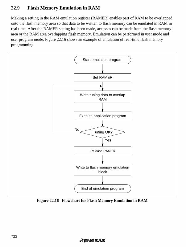
722
22.9 Flash Memory Emulation in RAM
Making a setting in the RAM emulation register (RAMER) enables part of RAM to be overlappedonto the flash memory area so that data to be written to flash memory can be emulated in RAM inreal time. After the RAMER setting has been made, accesses can be made from the flash memoryarea or the RAM area overlapping flash memory. Emulation can be performed in user mode anduser program mode. Figure 22.16 shows an example of emulation of real-time flash memoryprogramming.
Start emulation program
End of emulation program
Tuning OK?
Yes
No
Set RAMER
Write tuning data to overlapRAM
Execute application program
Write to flash memory emulationblock
Release RAMER
Figure 22.16 Flowchart for Flash Memory Emulation in RAM

723
H'000000
H'03F000
H'03F400
H'03F800
H'03FC00
H'03FFFF
EB0 to 7
EB11
EB10
EB9
EB8
H'FFFFF800
H'FFFFFBFF
On-chip RAM
Flash memory
This area can be accessed from both RAM and flash memory
Figure 22.17 Example of RAM Overlap Operation
Example in which Flash Memory Block Area (EB8) is Overlapped
1. Set bits RAMS, RAM1, and RAM0 in RAMER to 1, 0, 1, to overlap part of RAM onto thearea (EB8) for which real-time programming is required.
2. Real-time programming is performed using the overlapping RAM.
3. After the program data has been confirmed, the RAMS bit is cleared, releasing RAM overlap.
4. The data written in the overlapping RAM is written into the flash memory space (EB8).
Notes: 1. When the RAMS bit is set to 1, program/erase protection is enabled for all blocksregardless of the value of RAM1 and RAM0 (emulation protection). In this state,setting the P1 or E1 bit in flash memory control register 1 (FLMCR1), or the P2 or E2bit in flash memory control register 2 (FLMCR2), will not cause a transition toprogram mode or erase mode. When actually programming or erasing a flash memoryarea, the RAMS bit should be cleared to 0.
2. A RAM area cannot be erased by execution of software in accordance with the erasealgorithm while flash memory emulation in RAM is being used.

724
22.10 Note on Flash Memory Programming/Erasing
In the on-board programming modes (user mode and user program mode), NMI input should bedisabled to give top priority to the program/erase operations (including RAM emulation).
22.11 Flash Memory Programmer Mode
Programs and data can be written and erased in programmer mode as well as in the on-boardprogramming modes. In programmer mode, flash memory read mode, auto-program mode, auto-erase mode, and status read mode are supported. In auto-program mode, auto-erase mode, andstatus read mode, a status polling procedure is used, and in status read mode, detailed internalsignals are output after execution of an auto-program or auto-erase operation.
In programmer mode, set the mode pins to PLL x2 mode (see table 22.10) and use a 6 MHz inputclock. The LSI will then operate at 12 MHz.
Table 22.10 shows the pin settings for programmer mode. For the pin names in programmer mode,see section 1.3.2, Pin Arrangement by Mode).
Table 22.10 Programming Mode Pin Settings
Pin Names Settings
Mode pin: MD3, MD2, MD1, MD0 1101 (PLL × 2)
FWE pin High level input (in auto-program and auto-erase modes)
RES pin Power-on reset circuit
XTAL, EXTAL, PLLVcc, PLLCAP, and PLLVss pins Oscillator circuit
Note: During the programming mode, polarity of the FWP pin is inverted and becomes the FWE(flash write enable) pin.
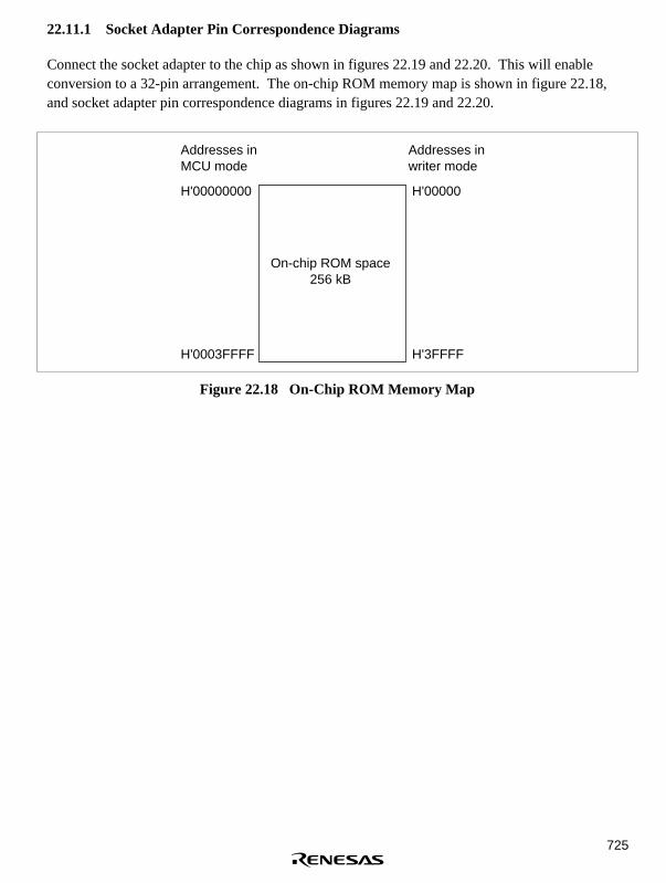
725
22.11.1 Socket Adapter Pin Correspondence Diagrams
Connect the socket adapter to the chip as shown in figures 22.19 and 22.20. This will enableconversion to a 32-pin arrangement. The on-chip ROM memory map is shown in figure 22.18,and socket adapter pin correspondence diagrams in figures 22.19 and 22.20.
H'00000000
Addresses in MCU mode
Addresses in writer mode
H'0003FFFF
H'00000
H'3FFFF
On-chip ROM space256 kB
Figure 22.18 On-Chip ROM Memory Map

726
Pin No.
77
13
20
19
44
70
69
68
67
66
64
63
62
4
5
6
7
8
9
10
11
12
43
14
15
16
17
18
42
21, 37, 46, 49, 50, 65, 73,
75, 76, 79, 100, 103
3, 23, 27, 33, 39, 55, 61, 71
78, 90, 91, 92, 93, 94, 95, 96,
97, 98, 99, 101, 109
26
84
72
74
80
81
82
Other than the above
Pin No.
1
26
2
3
31
13
14
15
17
18
19
20
21
12
11
10
9
8
7
6
5
27
24
23
25
4
28
29
22
32
16
30
HN28F101P (32 Pins)
Pin Name
FWE
A9
A16
A15
WE
I/O0
I/O1
I/O2
I/O3
I/O4
I/O5
I/O6
I/O7
A0
A1
A2
A3
A4
A5
A6
A7
A8
OE
A10
A11
A12
A13
A14
CE
VCC
VSS
A17
Pin Name
FWE
A9
A16
A15
WE
D0
D1
D2
D3
D4
D5
D6
D7
A0
A1
A2
A3
A4
A5
A6
A7
A8
OE
A10
A11
A12
A13
A14
CE
VSS
A17
RES
XTAL
EXTAL
PLLVCC
PLLCAP
PLLVSS
NC(OPEN)
HD64F7044 (112-Pin) Socket Adapter(Conversion to 32-Pin
Arrangement)
Power-on reset circuit
Oscillator circuit
PLL circuit
LegendFWE: Flash write enableI/O7–I/O0:Data input/outputA17–A0: Address inputOE: Output enableCE: Chip enableWE: Write enable
VCC
Figure 22.19 Socket Adapter Pin Correspondence Diagram (SH7044)

727
Pin No.
99
18
25
24
53
92
91
90
89
88
86
84
83
7
8
9
10
11
13
15
16
17
52
19
20
21
22
23
51
12, 26, 40, 63, 77, 85, 95,
97, 98, 103, 112, 127, 128,
131, 132, 135, 136
6, 14, 28, 35, 42, 55, 61,
71, 79, 87, 93, 102,
117 to 126, 129, 141
34
108
94
96
104
105
106
Other than the above
Pin No.
1
26
2
3
31
13
14
15
17
18
19
20
21
12
11
10
9
8
7
6
5
27
24
23
25
4
28
29
22
32
16
30
HN28F101P (32 Pins)
Pin Name
FWE
A9
A16
A15
WE
I/O0
I/O1
I/O2
I/O3
I/O4
I/O5
I/O6
I/O7
A0
A1
A2
A3
A4
A5
A6
A7
A8
OE
A10
A11
A12
A13
A14
CE
VCC
VSS
A17
Pin Name
FWE
A9
A16
A15
WE
D0
D1
D2
D3
D4
D5
D6
D7
A0
A1
A2
A3
A4
A5
A6
A7
A8
OE
A10
A11
A12
A13
A14
CE
VSS
A17
RES
XTAL
EXTAL
PLLVCC
PLLCAP
PLLVSS
NC(OPEN)
HD64F7045 (144-Pin) Socket Adapter(Conversion to 32-Pin
Arrangement)
Power-on reset circuit
Oscillator circuit
PLL circuit
LegendFWE: Flash write enableI/O7–I/O0:Data input/outputA17–A0: Address inputOE: Output enableCE: Chip enableWE: Write enable
VCC
Figure 22.20 Socket Adapter Pin Correspondence Diagram (SH7045)

728
22.11.2 Programmer Mode Operation
Table 22.11 shows how the different operating modes are set when using programmer mode, andtable 22.12 lists the commands used in programmer mode. Details of each mode are given below.
• Memory Read Mode
Memory read mode supports byte reads.
• Auto-Program Mode
Auto-program mode supports programming of 128 bytes at a time. Status polling is used toconfirm the end of auto-programming.
• Auto-Erase Mode
Auto-erase mode supports automatic erasing of the entire flash memory. Status polling is usedto confirm the end of auto-programming.
• Status Read Mode
Status polling is used for auto-programming and auto-erasing, and normal termination can beconfirmed by reading the I/O6 signal. In status read mode, error information is output if anerror occurs.
Table 22.11 Settings for Various Operating Modes In Programmer Mode
Pin names
Mode FWE CE OE WE I/O7–0 A17–0
Read H or L L L H Data output Ain
Output disable H or L L H H Hi-z Ain
Command write H or L L H L Data input * Ain
Chip disable H or L H X X Hi-z Ain
Notes: * Ain indicates that there is also address input in auto-program mode.1. Chip disable is not a standby state; internally, it is an operation state.2. For command writes in auto-program and auto-erase modes, input a high level to the
FWE pin.

729
Table 22.12 Commands of the Programmer Mode
Number First Cycle Second Cycle
Command Name of Cycles Mode Address Data Mode Address Data
Memory read mode 1+n write X H'00 read RA Dout
Auto-program mode 129 write X H'40 write WA Din
Auto-erase mode 2 write X H'20 write X H'20
Status read mode 2 write X H'71 write X H'71
Notes: 1. In auto-program mode, 129 cycles are required for command writing by a simultaneous128-byte write.
2. In memory read mode, the number of cycles depends on the number of address writecycles (n).
22.11.3 Memory Read Mode
Table 22.13 AC Characteristics in Transition to Memory Read Mode(Conditions: VCC = 5.0 V ±10%, VSS = 0 V, Ta = 25°C ±5°C)
Item Symbol Min Max Unit Notes
Command write cycle tnxtc 20 µs
CE hold time tceh 0 ns
CE setup time tces 0 ns
Data hold time tdh 50 ns
Data setup time tds 50 ns
Write pulse width twep 70 ns
WE rise time tr 30 ns
WE fall time tf 30 ns

730
CE
OE
CE
A16-0
OE
WE
I/O7-0
Note: Data is latched on the rising edge of WE.
tceh
twep
tf tr
tces tnxtc
Address stable
tds tdh
Command write Memory read mode
Figure 22.21 Timing Waveforms for Memory Read after Memory Write
Table 22.14 AC Characteristics in Transition from Memory Read Mode to Another Mode(Conditions: VCC = 5.0 V ±10%, VSS = 0 V, Ta = 25°C ±5°C)
Item Symbol Min Max Unit Notes
Command write cycle tnxtc 20 µs
CE hold time tceh 0 ns
CE setup time tces 0 ns
Data hold time tdh 50 ns
Data setup time tds 50 ns
Write pulse width twep 70 ns
WE rise time tr 30 ns
WE fall time tf 30 ns
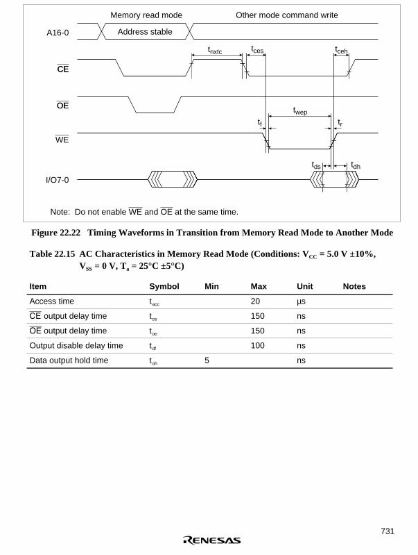
731
CE
OE
CE
A16-0
OE
WE
I/O7-0
Note: Do not enable WE and OE at the same time.
tceh
twep
tf tr
tcestnxtc
Address stable
tds tdh
Other mode command writeMemory read mode
Figure 22.22 Timing Waveforms in Transition from Memory Read Mode to Another Mode
Table 22.15 AC Characteristics in Memory Read Mode (Conditions: VCC = 5.0 V ±10%,VSS = 0 V, Ta = 25°C ±5°C)
Item Symbol Min Max Unit Notes
Access time tacc 20 µs
CE output delay time tce 150 ns
OE output delay time toe 150 ns
Output disable delay time tdf 100 ns
Data output hold time toh 5 ns

732
CE
A16-0
OE
WE
I/O7-0
VIL
VIL
VIH tacc tacctoh toh
Address stableAddress stable
Figure 22.23 CE and OE Enable State Read Timing Waveforms
CE
A16-0
OE
WE
I/O7-0
VIH tacc
tce
toe toe
tce
tacc
tohtdf
tdftoh
Address stableAddress stable
Figure 22.24 CE and OE Clock System Read Timing Waveforms
733
22.11.4 Auto-Program Mode
1. In auto-program mode, 128 bytes are programmed simultaneously. This should be carried outby executing 128 consecutive byte transfers.
2. A 128-byte data transfer is necessary even when programming fewer than 128 bytes. In thiscase, H'FF data must be written to the extra addresses.
3. The lower 8 bits of the transfer address must be H'00 or H'80. If a value other than an effectiveaddress is input, processing will switch to a memory write operation but a write error will beflagged.
4. Memory address transfer is performed in the second cycle (figure 22.24). Do not performtransfer after the second cycle.
5. Do not perform a command write during a programming operation.
6. Perform one auto-program operation for a 128-byte block for each address. Characteristics arenot guaranteed for two or more additional programming operations.
7. Confirm normal end of auto-programming by checking I/O6. Alternatively, status read modecan also be used for this purpose (I/O7 status output uses the auto-program operation endidentification pin).
8. Status polling I/O6 and I/O7 pin information is retained until the next command write. As longas the next command write has not been performed, reading is possible by enabling CE andOE.

734
Table 22.16 AC Characteristics in Auto-Program Mode (Conditions: VCC = 5.0 V ±10%,VSS = 0 V, Ta = 25°C ±5°C)
Item Symbol Min Max Unit Notes
Command write cycle tnxtc 20 µs
CE hold time tceh 0 ns
CE setup time tces 0 ns
Data hold time tdh 50 ns
Data setup time tds 50 ns
Write pulse width twep 70 ns
Status polling start time twsts 1 ms
Status polling access time tspa 150 ns
Address setup time tas 0 ns
Address hold time tah 60 ns
Memory write time twrite 1 3000 ms
Write setup time tpns 100 ns
Write end setup time tpnh 100 ns
WE rise time tr 30 ns
WE fall time tf 30 ns
CE
A16-0
FWE
OE
WE
I/O7
I/O6
I/O5-0
tpns
twep
tds tdh
tf tr tas tah twsts
twrite
tspa
tces tceh tnxtc tnxtc
tpnh
Address stable
H'40 H'00
Data transfer1 to 128byte
Write operation complete verify signal
Write normal complete verify signal
Figure 22.25 Auto-Program Mode Timing Waveforms

735
22.11.5 Auto-Erase Mode
1. Auto-erase mode supports only entire memory erasing.
2. Do not perform a command write during auto-erasing..
3. Confirm normal end of auto-erasing by checking I/O6. Alternatively, status read mode can alsobe used for this purpose (I/O7 status output uses the auto-erase operation end identificationpin).
4. Status polling I/O6 and I/O7 pin information is retained until the next command write. As longas the next command write has not been performed, reading is possible by enabling CE andOE.
Table 22.17 AC Characteristics in Auto-Erase Mode (Conditions: VCC = 5.0 V ±10%,VSS = 0 V, Ta = 25°C ±5°C)
Item Symbol Min Max Unit Notes
Command write cycle tnxtc 20 µs
CE hold time tceh 0 ns
CE setup time tces 0 ns
Data hold time tdh 50 ns
Data setup time tds 50 ns
Write pulse width twep 70 ns
Status polling start time tests 1 ms
Status polling access time tspa 150 ns
Memory erase time terase 100 40000 ms
Erase setup time tens 100 ns
Erase end setup time tenh 100 ns
WE rise time tr 30 ns
WE fall time tf 30 ns

736
CE
A16-0
FWE
OE
WE
I/O7
I/O6
I/O5-0
tens
twep
tds tdh
tf tr tests
terase
tspa
tces tceh tnxtc tnxtc
tenh
H'20 H'20 H'00
Erase complete
verify signal
Erase normal complete
verify signal
Figure 22.26 Auto-Erase Mode Timing Waveforms
22.11.6 Status Read Mode
Table 22.18 AC Characteristics in Status Read Mode (Conditions: VCC = 5.0 V ±10%,VSS = 0 V, Ta = 25°C ±5°C)
Item Symbol Min Max Unit Notes
Read time after command write tstd 20 µs
CE hold time tceh 0 ns
CE setup time tces 0 ns
Data hold time tdh 50 ns
Data setup time tds 50 ns
Write pulse width twep 70 ns
OE output delay time toe 150 ns
Disable delay time tdf 100 ns
CE output delay time tce 150 ns
WE rise time tr 30 ns
WE fall time tf 30 ns

737
CE
A16-0
OE
WE
I/O7-0
tweptf tr toe
tdftdstds tdhtdh
tces tceh
tce
tcehtnxtc tnxtc tnxtctces
H'71
twep
tf tr
H'71
Note : I/O2 and I/O3 are undefined.
Figure 22.27 Status Read Mode Timing Waveforms
Table 22.19 Return Commands for the Status Read Mode
Pin Name I/O7 I/O6 I/O5 I/O4 I/O3 I/O2 I/O1 I/O0
Attribute Normalendidentification
Commanderror
Program-ming error
Eraseerror
— — Program-ming orerase countexceeded
Effectiveaddress error
Initial value 0 0 0 0 0 0 0 0
Indications Normalend: 0
Abnormalend: 1
Command
Error: 1
Otherwise: 0
Program-ming
Error: 1
Otherwise: 0
Erasing
Error: 1
Otherwise: 0
— — Countexceeded: 1
Otherwise: 0
Effectiveaddress
Error: 1
Otherwise: 0
Note: D2 and D3 are undefined at present.
22.11.7 Status Polling
1. I/O7 status polling is a flag that indicates the operating status in auto-program/auto-erasemode.
2. I/O6 status polling is a flag that indicates a normal or abnormal end in auto-program/auto-erasemode.

738
Table 22.20 Status Polling Output Truth Table
Pin NameDuring InternalOperation Abnormal End Normal End
I/O7 0 1 0 1
I/O6 0 0 1 1
I/O5–0 0 0 0 0
22.11.8 Programmer Mode Transition Time
Commands cannot be accepted during the oscillation stabilization period or the programmer modesetup period. After the programmer mode setup time, a transition is made to memory read mode.
Table 22.21 Stipulated Transition Times to Command Wait State
Item Symbol Min Max Unit Notes
Standby release(oscillation stabilization time)
tOSC1 10 ms
Programmer mode setup time tbmv 10 ms
VCC hold time tdwn 0 ms
tOSC1 tbmv tdwn
VCC
RES
FWE
Memory read modeCommand wait state
Automatic write modeAutomatic erase mode
Command wait stateNormal/abnormal complete verify
Note : For the level of FWE input pin, set VIL when using other than the automatic write mode and automatic erase mode.
Figure 22.28 Oscillation Stabilization Time and Boot Program Transfer Time

739
22.11.9 Cautions Concerning Memory Programming
1. When programming addresses which have previously been programmed, carry out auto-erasing before auto-programming.
2. When performing programming using PROM mode on a chip that has beenprogrammed/erased in an on-board programming mode, auto-erasing is recommended beforecarrying out auto-programming.
Notes: 1. The flash memory is initially in the erased state when the device is shipped by RenesasTechnology. For other chips for which the erasure history is unknown, it isrecommended that auto-erasing be executed to check and supplement the initialization(erase) level.
2. Auto-programming should be performed once only on the same address block.Additional programming cannot be performed on previously programmed addressblocks.

740

741
Section 23 RAM
23.1 Overview
The SH7040 series has 4 kbytes of on-chip RAM. The on-chip RAM is linked to the CPU anddirect memory access controller (DMAC)/data transfer controller (DTC) with a 32-bit data bus(figure 23.1). The CPU can access data in the on-chip RAM in 8, 16, or 32 bit widths. The DMACcan access 8 or 16 bit widths. On-chip RAM data can always be accessed in one state, making theRAM ideal for use as a program area, stack area, or data area, which require high-speed access.The contents of the on-chip RAM are held in both the sleep and standby modes. Memory area 0addresses H'FFFFF000–H'FFFFFFFF are allocated to the on-chip RAM.
H'FFFFF000
H'FFFFF004
H'FFFFF001
H'FFFFF005
H'FFFFF002
H'FFFFF006
H'FFFFF003
H'FFFFF007
H'FFFFFFFC H'FFFFFFFD H'FFFFFFFE H'FFFFFFFF
On-chip RAM
Internal data bus (32 bits)
Figure 23.1 Block Diagram of RAM
23.2 Operation
The on-chip RAM is accessed by accessing addresses H'FFFFF000–H'FFFFFFFF. On-chip RAMis also used as cache memory. There are 2 kbytes of on-chip RAM space during cache use. Seesection 9, Cache Memory (CAC), for details.

742

743
Section 24 Power-Down State
24.1 Overview
In the power-down state, the CPU functions are halted. This enables a great reduction in powerconsumption.
24.1.1 Power-Down States
The power-down state is effected by the following two modes:
• Sleep mode
• Standby mode
Table 24.1 describes the transition conditions for entering the modes from the program executionstate as well as the CPU and peripheral function status in each mode and the procedures forcanceling each mode.
Table 24.1 Power-Down State Conditions
State
ModeEnteringProcedure Clock CPU
On-ChipPeripheralModules
CPURegisters RAM
I/OPorts
CancelingProcedure
Sleep Execute SLEEPinstruction withSBY bit set to 0in SBYCR
Run Halt Run Held Held Held • Interrupt• DMAC/DTC
address error• Power-on
reset• Manual reset
Stand-by
Execute SLEEPinstruction withSBY bit set to 1in SBYCR
Halt Halt Halt* 1 Held Held Held orhighimpe-dance* 2
• NMI interrupt• Power-on
reset• Manual reset
Notes: SBYCR: standby control register. SBY: standby bit* 1 Some bits within on-chip peripheral module registers are initialized by the standby
mode; some are not. Refer to table 24.3, Register States in the Standby Mode, insection 24.4.1, Transition to Standby Mode. Also refer to the register descriptions foreach peripheral module.
* 2 The status of the I/O port in standby mode is set by the port high impedance bit (HIZ) ofthe SBYCR. Refer to section 24.2, Standby Control Register (SBYCR). For pin statusother than for the I/O port, refer to Appendix C, Pin Status.

744
24.1.2 Related Register
Table 24.2 shows the register used for power-down state control.
Table 24.2 Related Register
Name Abbreviation R/W Initial Value Address Access Size
Standby control register SBYCR R/W H'1F H'FFFF8614 8, 16, 32
24.2 Standby Control Register (SBYCR)
The standby control register (SBYCR) is a read/write 8-bit register that sets the transition tostandby mode, and the port status in standby mode. The SBYCR is initialized to H'1F when reset.
Bit: 7 6 5 4 3 2 1 0
SBY HIZ — — — — — —
Initial value: 0 0 0 1 1 1 1 1
R/W: R/W R/W R R R R R R
• Bit 7—Standby (SBY): Specifies transition to the standby mode. The SBY bit cannot be set to1 while the watchdog timer is running (when the timer enable bit (TME) of the WDT timercontrol/status register (TCSR) is set to 1). To enter the standby mode, always halt the WDT by0 clearing the TME bit, then set the SBY bit.
Bit 7: SBY Description
0 Executing SLEEP instruction puts the LSI into sleep mode (initial value)
1 Executing SLEEP instruction puts the LSI into standby mode
• Bit 6—Port High Impedance (HIZ): In the standby mode, this bit selects whether to set the I/Oport pin to high impedance or hold the pin status. The HIZ bit cannot be set to 1 when the TMEbit of the WDT timer control/status register (TCSR) is set to 1. When making the I/O port pinstatus high impedance, always clear the TME bit to 0 before setting the HIZ bit.
Bit 6: HIZ Description
0 Holds pin status while in standby mode (initial value)
1 Keeps pin at high impedance while in standby mode
• Bits 5–0—Reserved: Bit 5 always reads as 0. Always write 0 to bit 5. Bits 4–0 always read as1. Always write 1 to these bits.

745
24.3 Sleep Mode
24.3.1 Transition to Sleep Mode
Executing the SLEEP instruction when the SBY bit of SBYCR is 0 causes a transition from theprogram execution state to the sleep mode. Although the CPU halts immediately after executingthe SLEEP instruction, the contents of its internal registers remain unchanged. The on-chipperipheral modules continue to run during the sleep mode.
24.3.2 Canceling Sleep Mode
Sleep mode is canceled by an interrupt, DMAC/DTC address error, power-on reset, or manualreset.
Cancellation by an Interrupt: When an interrupt occurs, the sleep mode is canceled and interruptexception processing is executed. The sleep mode is not canceled if the interrupt cannot beaccepted because its priority level is equal to or less than the mask level set in the CPU’s statusregister (SR) or if an interrupt by an on-chip peripheral module is disabled at the peripheralmodule.
Cancellation by a DMAC/DTC Address Error: If a DMAC/DTC address error occurs, the sleepmode is canceled and DMAC/DTC address error exception processing is executed.
Cancellation by a Power-On Reset: A power-on reset resulting from setting the RES pin to lowlevel cancels the sleep mode.
Cancellation by a Manual Reset: When the MRES pin is set to low level while the RES pin is athigh level, a manual reset occurs and the sleep mode is canceled.
24.4 Standby Mode
24.4.1 Transition to Standby Mode
To enter the standby mode, set the SBY bit to 1 in SBYCR, then execute the SLEEP instruction.The LSI moves from the program execution state to the standby mode. In the standby mode,power consumption is greatly reduced by halting not only the CPU, but the clock and on-chipperipheral modules as well. CPU register contents and on-chip RAM data are held as long as theprescribed voltages are applied. The register contents of some on-chip peripheral modules areinitialized, but some are not (table 24.3). The I/O port status can be selected as held or highimpedance by the port high impedance bit (HIZ) of the SBYCR. For pin status other than for theI/O port, refer to Appendix C, Pin States.

746
Table 24.3 Register States in the Standby Mode
Module Registers InitializedRegisters thatRetain Data
Registers withUndefined Contents
Interrupt controller(INTC)
— All registers —
User break controller(UBC)
— All registers —
Data transfer controller(DTC)
All registers (excluding transferdata in memory and DTDR)
— —
Cache memory (CAC) — All registers —
Bus state controller(BSC)
— All registers —
Direct memory accesscontroller (DMAC)
• DMA channel controlregisters 0–3 (CHCR0–CHCR3)
• DMA operation register(DMAOR)
— • DMA sourceaddress registers0–3 (SAR0–SAR3)
• DMA destinationaddress registers0–3 (DAR0–DAR3)
• DMA transfercount registers0–3 (DMATCR0–DMATCR3)
Multifunction timerpulse unit (MTU)
MTU associated registers POE associatedregisters
—
Watchdog timer(WDT)
• Bits 7–5 (OVF, WT/IT, TME)of the timer control statusregister (TCSR)
• Reset control/status register(RSTCSR)
• Bits 2–0(CKS2–CKS0)of the TCSR
• Timer counter(TCNT)
—
Serial communicationinterface (SCI)
• Receive data register (RDR)• Transmit data register (TDR)• Serial mode register (SMR)• Serial control register (SCR)• Serial status register (SSR)• Bit rate register (BBR)
— —
A/D converter (A/D) All registers — —
Compare match timer(CMT)
All registers — —

747
Table 24.3 Register States in the Standby Mode (cont)
Module Registers InitializedRegisters thatRetain Data
Registers withUndefined Contents
Pin function controller(PFC)
— All registers —
I/O port (I/O) — All registers —
Power-down staterelated
— Standby controlregister (SBYCR)
—
24.4.2 Canceling the Standby Mode
The standby mode is canceled by an NMI interrupt, a power-on reset, or a manual reset.
Cancellation by an NMI: Clock oscillation starts when a rising edge or falling edge (selected bythe NMI edge select bit (NMIE) of the interrupt control register (ICR) of the INTC) is detected inthe NMI signal. This clock is supplied only to the watchdog timer (WDT). A WDT overflowoccurs if the time established by the clock select bits (CKS2–CKS0) in the TCSR of the WDTelapses before transition to the standby mode. The occurrence of this overflow is used to indicatethat the clock has stabilized, so the clock is supplied to the entire chip, the standby mode iscanceled, and NMI exception processing begins.
When canceling standby mode with NMI interrupts, set the CKS2–CKS0 bits so that the WDToverflow period is longer than the oscillation stabilization time.
When canceling standby mode with an NMI pin set for falling edge, be sure that the NMI pin levelupon entering standby (when the clock is halted) is high level, and that the NMI pin level uponreturning from standby (when the clock starts after oscillation stabilization) is low level. Whencanceling standby mode with an NMI pin set for rising edge, be sure that the NMI pin level uponentering standby (when the clock is halted) is low level, and that the NMI pin level upon returningfrom standby (when the clock starts after oscillation stabilization) is high level.
Cancellation by a Power-On Reset: A power-on reset caused by setting the RES pin to low levelcancels the standby mode.

748
24.4.3 Standby Mode Application Example
This example describes a transition to standby mode on the falling edge of an NMI signal, and acancellation on the rising edge of the NMI signal. The timing is shown in figure 24.1.
When the NMI pin is changed from high to low level while the NMI edge select bit (NMIE) of theICR is set to 0 (falling edge detection), the NMI interrupt is accepted. When the NMIE bit is set to1 (rising edge detection) by an NMI exception service routine, the standby bit (SBY) of theSBYCR is set to 1, and a SLEEP instruction is executed, standby mode is entered. Thereafter,standby mode is canceled when the NMI pin is changed from low to high level.
Oscillator
CK
NMI
NMIE
SBY
NMIexceptionprocessing
Exceptionserviceroutine
SBY = 1SLEEP
instruction
Standbymode
Oscillationstarttime
WDTtimeset
NMIexception processing
Oscillationsettling time
Figure 24.1 Standby Mode NMI Timing (Application Example)
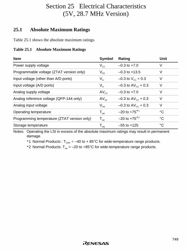
749
Section 25 Electrical Characteristics(5V, 28.7 MHz Version)
25.1 Absolute Maximum Ratings
Table 25.1 shows the absolute maximum ratings.
Table 25.1 Absolute Maximum Ratings
Item Symbol Rating Unit
Power supply voltage VCC –0.3 to +7.0 V
Programmable voltage (ZTAT version only) VPP –0.3 to +13.5 V
Input voltage (other than A/D ports) Vin –0.3 to VCC + 0.3 V
Input voltage (A/D ports) Vin –0.3 to AVCC + 0.3 V
Analog supply voltage AVCC –0.3 to +7.0 V
Analog reference voltage (QFP-144 only) AVref –0.3 to AVCC + 0.3 V
Analog input voltage VAN –0.3 to AVCC + 0.3 V
Operating temperature Topr –20 to +75* 1 °C
Programming temperature (ZTAT version only) Twe –20 to +75* 2 °C
Storage temperature Tstg –55 to +125 °C
Notes: Operating the LSI in excess of the absolute maximum ratings may result in permanentdamage.* 1 Normal Products : TOPR = –40 to + 85°C for wide-temperature range products.* 2 Normal Products: Twe = –20 to +85°C for wide-temperature range products.

750
25.2 DC Characteristics
Table 25.2 DC Characteristics (Conditions: VCC = 5.0 V ± 10%, AVCC = 5.0 V ± 10%,AVCC = VCC ± 10%, AVref = 4.5 V to AVCC, VSS = AVSS = 0 V, Ta = –20 to +75° C)
Item Pin Symbol Min Typ Max UnitMeasurementConditions
Input high-levelvoltage
RES, NMI, MD3–MD0, PA2, PA5,PA6–PA9, PE0–PE15, FWP
VIH VCC – 0.7 — VCC + 0.3 V —
EXTAL VCC × 0.7 — VCC + 0.3 V —
A/D port 2.2 — AVCC + 0.3 V —
Other input pins 2.2 — VCC + 0.3 V —
Input low-levelvoltage
RES, NMI, MD3–MD0, PA2, PA5,PA6–PA9, PE0–PE15, FWP
VIL –0.3 — 0.5 V —
Other input pins –0.3 — 0.8 V —
Schmitttrigger inputvoltage
PA2, PA5, PA6–PA9, PE0–PE15
VT+ – VT–0.4 — — V VT+ ≥ VCC – 0.7 V (min)
VT– ≤ 0.5 V (max)
Input leakcurrent
RES, NMI, MD3–MD0, PA2, PA5,PA6–PA9, PE0–PE15,FWP
| Iin | — — 1.0 µA Vin = 0.5 to VCC – 0.5 V
A/D port — — 1.0 µA Vin = 0.5 to AVCC – 0.5 V
Other input pins(except EXTALpin)
— — 1.0 µA Vin = 0.5 to VCC – 0.5 V
Three-stateleak current(while off)
A21–A0, D31–D0, CS3–CS0,RDWR, RAS,CASxx, WRxx,RD, ports A, B, C,D, E
| ITSI | — — 1.0 µA Vin = 0.5 to VCC – 0.5 V

751
Table 25.2 DC Characteristics (Conditions: VCC = 5.0 V ± 10%, AVCC = 5.0 V ± 10%,AVCC = VCC ± 10%, AVref = 4.5 V to AVCC, VSS = AVSS = 0 V, Ta = –20 to +75°C)(cont)
Item Pin Symbol Min Typ Max UnitMeasurementConditions
Output All output pins VOH VCC – 0.5 — — V IOH = –200 µAhigh-levelvoltage
3.5 — — V IOH = –1 mA
Output low- All output pins VOL — — 0.4 V IOL = 1.6 mAlevelvoltage
PE9, PE11–PE15 — — 1.5 V IOL = 15 mA
Input RES Cin — — 80* 1 pF Vin = 0 V, f = 1 MHz,capaci- NMI — — 50 pF Ta = 25°Ctance
All other inputpins
— — 20 pF
Currentconsump-
Ordinaryoperation
ICC — 160 230 mA f = 28 MHz
tion Sleep — 140 200 mA f = 28 MHz
Standby — 0.01 5 µA Ta ≤ 50°C
— — 20 µA Ta > 50°C
Analog AICC — 5 10 mAsupplycurrent
AIref — 0.5 1* 2 mA QFP144 version only
RAMstandbyvoltage
VRAM 2.0 — — V
Notes: 1. When the A/D converter is not used (including during standby), do not release the AVCC,AVSS, and AVref (SH7041,SH7043,SH7045 only) pins. Connect the AVCC and AVref
(SH7041,SH7043,SH7045 only) pins to VCC and the AVSS pin to VSS.2. The current consumption is measured when VIHmin = VCC – 0.5 V, VIL max = 0.5 V, with
all output pins unloaded.3. The ZTAT and mask versions as well as F-ZTAT and mask versions have the same
functions, and the electrical characteristics of both are within specification, butcharacteristic-related performance values, operating margins, noise margins, noiseemission, etc., are different. Caution is therefore required in carrying out system design,when switching between ZTAT and mask versions, and when switching between F-ZTAT and mask versions.
4. When the SH7040 chip is used for high-speed operation, the package surfacetemperature rises. Appropriate measures (such as heat dissipation) to ensure overallsystem reliability and safety should therefore be investigated.
* 1 110pF for A mask* 2 5 mA in the A mask version, except for F-ZTAT products.

752
Table 25.3 Permitted Output Current Values (Conditions: VCC = 5.0 V ± 10%, AVCC =5.0 V ± 10%, AVCC = VCC ± 10%, AVref = 4.5 V to AVCC, VSS = AVSS = 0 V,Ta = –20 to +75° C)
Item Symbol Min Typ Max Unit
Output low-level permissible current (per pin) IOL — — 2.0* mA
Output low-level permissible current (total) ∑ IOL — — 80 mA
Output high-level permissible current (per pin) –IOH — — 2.0 mA
Output high-level permissible current (total) ∑ (–IOH) — — 25 mA
Notes: To assure LSI reliability, do not exceed the output values listed in this table.* PE9, PE11–PE15 are IOL = 15 mA (max). Make sure that no more than three of these
pins exceed an IOL of 2.0 mA simultaneously.
25.3 AC Characteristics
25.3.1 Clock Timing
Table 25.4 Clock Timing (Conditions: VCC = 5.0 V ± 10%, AVCC = 5.0 V ± 10%, AVCC =VCC ± 10%, AVref = 4.5 V to AVCC, VSS = AVSS = 0 V, Ta = –20 to +75° C)
Item Symbol Min Max Unit Figures
Operating frequency fOP 4 28.7 MHz 25.1
Clock cycle time tcyc 34.8 250 ns
Clock low-level pulse width tCL 10 — ns
Clock high-level pulse width tCH 10 — ns
Clock rise time tCR — 5 ns
Clock fall time tCF — 5 ns
EXTAL clock input frequency fEX 4 10 MHz 25.2
EXTAL clock input cycle time tEXcyc 100 250 ns
EXTAL clock low-level input pulse width tEXL 40 — ns
EXTAL clock high-level input pulse width tEXH 40 — ns
EXTAL clock input rise time tEXR — 5 ns
EXTAL clock input fall time tEXF — 5 ns
Reset oscillation settling time tOSC1 10 — ms 25.3
Standby return clock settling time tOSC2 10 — ms

753
tcyc
tCLtCH
1/2VCC 1/2VCC
tCF tCR
CK
Figure 25.1 System Clock Timing
tEXcyc
tEXLtEXH
VIH VIH1/2VCC VIL VIL
1/2VCC
tEXF tEXR
EXTAL VIH
Figure 25.2 EXTAL Clock Input Timing
tOSC1
VCC min
tOSC2
CK
VCC
RES
Figure 25.3 Oscillation Settling Time

754
25.3.2 Control Signal Timing
Table 25.5 Control Signal Timing (Conditions: VCC = 5.0 V ± 10%, AVCC = 5.0 V ± 10%,AVCC = VCC ± 10%, AVref = 4.5 V to AVCC, VSS = AVSS = 0 V, Ta = –20 to +75° C)
Item Symbol Min Max Unit Figure
RES rise/fall tRESr, tRESf — 200 ns 25.4
RES pulse width tRESW 20 — tcyc
MRES pulse width tMRESW 20 — tcyc
NMI rise/fall tNMIr, tNMIf — 200 ns 25.5
RES setup time* tRESS 35 — ns 25.4,
MRES setup time* tMRESS 35 — ns 25.5
NMI setup time* tNMIS 35 — ns
IRQ7–IRQ0 setup time (edge detection) tIRQES 35 — ns
IRQ7–IRQ0 setup time (level detection) tIRQLS 35 — ns
NMI hold time tNMIH 35 — ns 25.5
IRQ7–IRQ0 hold time tIRQEH 35 — ns
IRQOUT output delay time tIRQOD — 35 ns 25.6
Bus request setup time tBRQS 35 — ns 25.7
Bus acknowledge delay time 1 tBACKD1 — 35 ns
Bus acknowledge delay time 2 tBACKD2 — 35 ns
Bus three-state delay time tBZD — 35 ns
Note: * The RES, MRES, NMI, BREQ, and IRQ7–IRQ0 signals are asynchronous inputs, butwhen thesetup times shown here are provided, the signals are considered to haveproduced changes at clock rise (for RES, MRES, BREQ) or clock fall (for NMI and IRQ7–IRQ0). If the setup times are not provided, recognition is delayed until the next clock riseor fall.

755
CK
RES
MRES
tRESf
tRESW
tMRESW
tRESr
tRESS
tMRESS tMRESS
tRESS
VIH VIH
VIH
VIL VIL
VIL VIL
Figure 25.4 Reset Input Timing
tNMIH tNMIS
tNMIr,tNMIf
VIH
VIL
tIRQEH tIRQES
VIH
VIL
tIRQLS
CK
NMI
IRQ edge
IRQ level
Figure 25.5 Interrupt Signal Input Timing

756
tIRQODtIRQOD
CK
IRQOUT
Figure 25.6 Interrupt Signal Output Timing
CK
RD, RDWR, RAS, CASxx,
CSn, WRxx
A21–A0,D31–D0
tBRQStBRQS
tBACKD1 tBACKD2
tBZD
tBZD
BREQ (Input)
Note: During the bus-release period of a self-refresh, RAS, CASx, and RDWR are output.
BACK (Output)
Figure 25.7 Bus Right Release Timing

757
25.3.3 Bus Timing
Table 25.6 Bus Timing (Conditions: VCC = 5.0 V ± 10%, AVCC = 5.0 V ± 10%, AVCC = VCC ±10%, AVref = 4.5 V – AVCC , VSS = AVSS = 0 V, Ta = – 20 to +75°C)
Item Symbol Min Max Unit Figure
Address delay time tAD 2* 3 18 ns 25.8, 25.9,25.11–25.16,25.19
CS delay time 1 tCSD1 2* 3 21 ns 25.8, 25.9, 25.19
CS delay time 2 tCSD2 2* 3 21 ns
Read strobe delay time 1 tRSD1 2* 3 18 ns 25.8, 25.9,
Read strobe delay time 2 tRSD2 2* 3 18 ns 25.11–25.16,
Read data setup time tRDS* 4 15 — ns
25.19
Read data hold time tRDH 0 — ns
Write strobe delay time 1 tWSD1 2* 3 18 ns
Write strobe delay time 2 tWSD2 2* 3 18 ns
Write data delay time tWDD — 35 ns
Write data hold time tWDH 0 10* 2 ns
WAIT setup time tWTS 15 — ns 25.10, 25.15,
WAIT hold time tWTH 0 — ns 25.19
RAS delay time 1 tRASD1 2* 3 18 ns 25.11–25.18
RAS delay time 2 tRASD2 2* 3 18 ns
CAS delay time 1 tCASD1 2* 3 18 ns
CAS delay time 2 tCASD2 2* 3 18 ns
Read data access time tACC* 1 tcyc × (n + 2) – 40 — ns 25.8, 25.9
Access time from read strobe tOE* 1 tcyc × (n + 1.5) – 40 — ns
Access time from columnaddress
tAA* 1 tcyc × (n + 2) – 40 — ns 25.11–25.16
Access time from RAS tRAC* 1 tcyc × (n + RCD + 2.5) – 40 — ns
Access time from CAS tCAC* 1 tcyc × (n + 1) – 40 — ns
Row address hold time tRAH tcyc × (RCD + 0.5) – 15 — ns
Row address setup time tASR* 5 tcyc × 0.5–17.5 — ns
Data input setup time tDS tcyc × (m + 0.5) – 25 — ns
Data input hold time tDH 20 — ns

758
Table 25.7 Bus Timing (Conditions: VCC = 5.0 V ± 10%, AVCC = 5.0 V ± 10%, AVCC = VCC ±10%, AVref = 4.5 V to AVCC, VSS = AVSS = 0 V, Ta = – 20 to +75°C)
Item Symbol Min Max Unit Figure
Write address setup time tAS 0 — ns 25.8–25.9
Write address hold time tWR 5 — ns 25.8, 25.9, 25.19
Write data hold time tWRH 0 — ns
Read/write strobe delay time 1 tRWD1 2* 3 18 ns 25.11–25.16
Read/write strobe delay time 2 tRWD2 2* 3 18 ns
High-speed page mode CASprecharge time
tCP tcyc – 25 — ns 25.16
RAS precharge time tRP tcyc × (TPC + 1.5) – 15 — ns 25.11–25.16
CAS setup time tCSR 10 — ns 25.17, 25.18
AH delay time 1 tAHD1 2* 3 18 ns 25.19
AH delay time 2 tAHD2 2* 3 18 ns
Multiplex address delay time tMAD 2* 3 18 ns
Multiplex address hold time tMAH 0 — ns
DACK delay time tDACKD1 2* 3 21 ns 25.8, 25.9, 25.11–25.16, 25.19
Notes: n is the number of waits. m is 0 when the number of DRAM write cycle waits is 0, and 1otherwise. RCD is the set value of the RCD bit in DCR. TPC is the set value of the TPC bitin DCR.* 1 If the access time is satisfied, tRDS need not be satisfied.* 2 tWDH (max) is a reference value.* 3 The delay time Min values are reference values (typ).* 4 tRDS is a reference value.* 5 When 28.7MHz, tASR=0ns (min)

759
T1 T2
CK
A21–A0
DACKn
tDACKD1 tDACKD1
tWDHtWDD
tWSD1 tWSD2
tACCtRDS tRDH
tRSD1 tOE tRSD2
tCSD2tCSD1
tAD
tAS
tWR
tWRH
CSn
Note: tRDH is specified from fastest negate timing of A21–A0, CSn, and RD.
(During read)
(During read)
RD
D31–D0
D31–D0
WRxx(During write)
(During write)
Figure 25.8 Basic Cycle (No Waits)
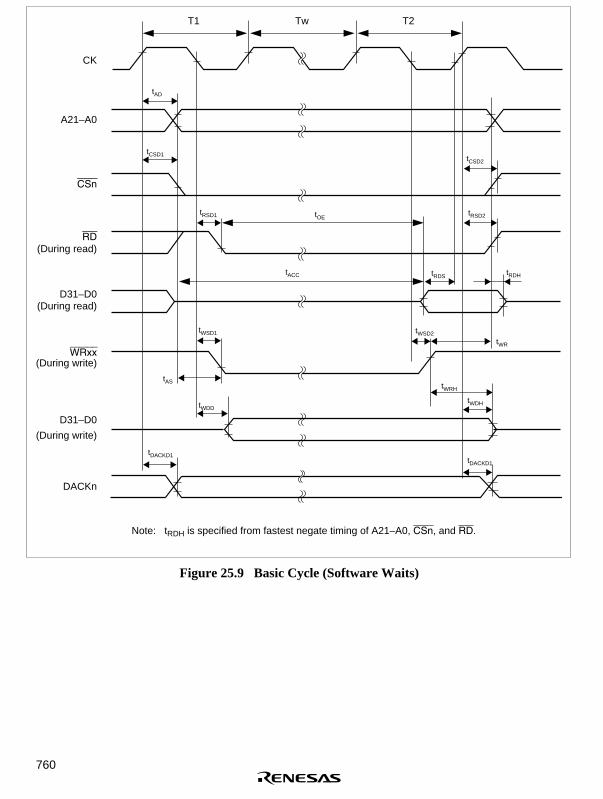
760
CK
A21–A0
DACKn
T1 Tw T2
tAD
tCSD1
tRSD1
tWSD1
tWDD
tDACKD1
tRSD2
tCSD2
tRDS tRDH
tWSD2
tWDH
tDACKD1
tOE
tACC
tAStWRH
tWR
Note: tRDH is specified from fastest negate timing of A21–A0, CSn, and RD.
CSn
RD
D31–D0
D31–D0
(During read)
(During read)
(During write)
(During write)WRxx
Figure 25.9 Basic Cycle (Software Waits)

761
CK
A21–A0
T1 Tw TwoTw T2
tWTS tWTH tWTS tWTH
CSn
RD
WRxx
WAIT
DACKn
(During read)
(During read)
(During write)
(During write)
D31–D0
D31–D0
Figure 25.10 Basic Cycle (2 Software Waits + Wait due to WAIT Signal)

762
Tp Tr Tc1 Tc2
tAD tAD
tASR
tRP
tRASD1tRAH
tCASD1
tCAC
tAA
tRAC
tRDS
tRASD2
tCASD2
tRDH
tRWD1
tCASD2tCASD1
tRWD2
tWDH
tDHtDS
tWDD
tDACKD1tDACKD1
tRSD1 tRSD2
tWSD1 tWSD2
CK
A21–A0
RAS
CASxx
RDWR
D31– D0
D31–D0
CASxx
RDWR
DACKn
RD
WRxx
Note: tRDH is specified from fastest negate timing of A21–A0, RAS, and CAS.
(During read)
(During read)
(During read)
(During read)
(During write)
(During write)
(During write)
(During write)
Row address Column address
Figure 25.11 DRAM Cycle (Normal Mode, No Waits, TPC = 0, RCD = 0)

763
Tp
CK
A21–A0
Tr Tc1 Tcw1 Tc2
tAD tAD
tRP
tRASD1tASR
tCASD1
tRAH tRASD2
tCASD2
tCAC
tRAC
tAAtRDS tRDH
tCASD2
tRWD2
tWDH
tDHtDS
tWDD
tDACKD1tDACKD1
tRSD1
tWSD1 tWSD2
tRSD2
tCASD1
tRWD1
Row address Column address
RAS
CASxx
RDWR
D31–D0
CASxx
RDWR
D31–D0
DACKn
RD
WRxx
Note: tRDH is specified from fastest negate timing of A21–A0, RAS, and CAS.
(During read)
(During read)
(During read)
(During read)
(During write)
(During write)
(During write)
(During write)
Figure 25.12 DRAM Cycle (Normal Mode, 1 Wait, TPC = 0, RCD = 0)

764
CK
A21–A0
Tp Tpw Tr Trw Tc1 Tcw1 Tcw2 Tc2
tAD tAD
tASR
tRASD1tRAH
tRP
tCASD1
tCAC
tAAtRAC
tRDS tRDH
tCASD2tCASD1
tRWD2tRWD1
tDHtDS
tWDH
tDACKD1tDACKD1
tWDD
tRSD1 tRSD2
tWSD1 tWSD2
tRASD2
tCASD2
RAS
CASxx
RDWR
D31–D0
CASxx
RDWR
D31–D0
DACKn
RD
WRxx
(During read)
(During read)
(During read)
(During read)
(During write)
(During write)
(During write)
(During write)
Row address Column address
Note: tRDH is specified from fastest negate timing of A21–A0, RAS, and CAS.
Figure 25.13 DRAM Cycle (Normal Mode, 2 Waits, TPC = 1, RCD = 1)
CK
A21–A0
Tp Tpw Tr Trw Tc1 Tcw1 Tcw2 Tcw3 Tc2
tAD tAD
tRAHtASR
tRP
tCASD1
tCAC
tAA
tCASD1
tRDS
tCASD2
tRWD2tRWD1
tDS tDHtWDH
tDACKD1
tRSD1
tWSD1tWSD2
tRSD2
tDACKD1
tRASD2
tCASD2
tWDD
RAS
CASxx
RDWR
D31–D0
CASxx
RDWR
D31–D0
DACKn
RD
WRxx
(During read)
(During read)
(During read)
(During read)
(During write)
(During write)
(During write)
(During write)
Row address Column addresstRASD1
tRDH
tRAC
Note: tRDH is specified from fastest negate timing of A21–A0, RAS, and CAS.
Figure 25.14 DRAM Cycle (Normal Mode, 3 Waits, TPC = 1, RCD = 1)

765
CK
A21–A0
Tp Tr Tc1 Tcw1 Tcw2 Tcwo Tc2
tAD tAD
tASRtRAH
tRASD1
tRP
tCASD1
tCAC
tAA
tRAC
tRDH
tCASD2
tRWD2
tCASD1
tWDH
tDHtDS
tRWD1
tWDD
tWTS tWTH tWTS tWTH
tDACKD1
tRSD2
tWSD2tWSD1
tRSD1
tRASD2
tDACKD1
tCASD2
tRDS
RAS
CASxx
RDWR
D31–D0
CASxx
RDWR
D31–D0
DACKn
RD
WRxx
WAIT
(During read)
(During read)
(During read)
(During read)
(During write)
(During write)
(During write)
(During write)
Row address Column address
Note: tRDH is specified from fastest negate timing of A21–A0, RAS, and CAS.
Figure 25.15 DRAM Cycle (Normal Mode, 2 Waits + Wait due to WAIT Signal)

766
CK
A21–A0
Tp Tr Tc1 Tc2 Tc1 Tc2
tAD tAD
tASR
tRASD1tRAH
tRPtCASD1 tCASD2 tCASD1 tCASD2
tRASD2
tCP
tAA
tCAC
tAAtRAC
tRDStRDH
tRDS tRDH
tCAC
tCASD1tCASD2tCASD1 tCASD2
tRWD2tRWD1tRWD2tRWD1
tDHtDS
tWDD tWDH tWDD tWDH
tDHtDS
tCP
tDACKD1 tDACKD1
tRSD1
tWSD1 tWSD2tWSD1 tWSD2
tRSD2 tRSD1 tRSD2
tDACKD1
RAS
CASxx
RDWR
D31–D0
CASxx
RDWR
D31–D0
DACKn
RD
WRxx
(During read)
(During read)
(During read)
(During read)
(During write)
(During write)
(During write)
(During write)
Note: tRDH is specified from fastest negate timing of A21–A0, RAS, and CAS.
Row address Column address Column address
Figure 25.16 DRAM Cycle (High-Speed Page Mode)
CK
RDWR
TRp TRr1 TRr2 TRc TRc
tRASD1tRASD2
tCASD2
tCSR
tCASD1
RAS
CASxx
Figure 25.17 CAS Before RAS Refresh (TRAS1 = 0, TRAS0 = 0)

767
CK
RAS
CASxx
RDWR
TRcc
tRASD2
tCASD2
tCSR
tCASD1
TRp TRr1 TRr2
tRASD1
TRc
Figure 25.18 Self Refresh
CK
A21–A0
DACKn
Ta1 Ta2 Ta3 Ta4 T1 TW TWo T2
tAD
tCSD1 tCSD2
tAHD1 tAHD2
tRSD2
tMAHtMAD tRDS tRDH
tMAH tWDDtMAD tWDH
tDACKD1tDACKD1
tWTS tWTH tWTS tWTH
tWSD2
tWR
tWRH
tRSD1
CS3
AH
D15–D0
WAIT
D15–D0
RD
WRxx
(During read)
Address
Address
(During read)
(During write)
(During write)
tWSD1
Note: tRDH is specified from fastest negate timing of A21–A0, CS3, and RD.
Figure 25.19 Address Data Multiplex I/O Space Cycle (1 Software Wait + External Wait)

768
25.3.4 Direct Memory Access Controller Timing
Table 25.8 Direct Memory Access Controller Timing (Conditions: VCC = 5.0 V ± 10%,AVCC = 5.0 V ± 10%, AVCC = VCC ± 10%, AVref = 4.5 V to AVCC, VSS = AVSS = 0V, Ta = – 20 to +75°C)
Item Symbol Min Max Unit Figure
DREQ0 and DREQ1 setup time tDRQS 18 — ns 25.20
DREQ0 and DREQ1 hold time tDRQH 18 — ns
DREQ0 and DREQ1 pulse width tDRQW 1.5 — tcyc 25.21
DRAK output delay time tDRAKD — 18 ns 25.22
CK
tDRQS
tDRQS
tDRQS
tDRQH
DREQ0DREQ1
Level clear
DREQ0DREQ1
Level
DREQ0DREQ1
Edge
Figure 25.20 DREQ0 and DREQ1 Input Timing (1)

769
CK
tDRQW
DREQ0DREQ1
Edge
Figure 25.21 DREQ0 and DREQ1 Input Timing (2)
CK
tDRAKD tDRAKD
DRAKn
Figure 25.22 DRAK Output Delay Time

770
25.3.5 Multifunction Timer Pulse Unit Timing
Table 25.9 Multifunction Timer Pulse Unit Timing (Conditions: VCC = 5.0 V ± 10%, AVCC
= 5.0 V ± 10%, AVCC = VCC ± 10%, AVref = 4.5 V to AVCC, VSS = AVSS = 0 V, Ta= – 20 to +75°C)
Item Symbol Min Max Unit Figure
Output compare output delay time tTOCD — 100 ns 25.23
Input capture input setup time tTICS 30 — ns
Timer input setup time tTCKS 35 — ns
Timer clock pulse width (singleedge specification)
tTCKWH/L 1.5 — tcyc 25.24
Timer clock pulse width (bothedges specified)
tTCKWH/L 2.5 — tcyc
Timer clock pulse width (phasemeasurement mode)
tTCKWH/L 2.5 — tcyc
CK
tTOCD
tTICS
Inputcapture input
Outputcompare output
Figure 25.23 MTU I/O Timing
CK
TCLKA to TCLKD
tTCKS tTCKS
tTCKWHtTCKWL
Figure 25.24 MTU Clock Input Timing

771
25.3.6 I/O Port Timing
Table 25.10 I/O Port Timing (Conditions: VCC = 5.0 V ± 10%, AVCC = 5.0 V ± 10%, AVCC =VCC ± 10%, AVref = 4.5 V to AVCC, VSS = AVSS = 0 V, Ta = – 20 to +75°C)
Item Symbol Min Max Unit Figure
Port output data delay time tPWD — 100 ns 25.25
Port input hold time tPRH 35 — ns
Port input setup time tPRS 35 — ns
tPRS tPRH
tPWD
T1 T2
CK
Port (Read)
Port (Write)
Figure 25.25 I/O Port I/O Timing

772
25.3.7 Watchdog Timer Timing
Table 25.11 Watchdog Timer Timing (Conditions: VCC = 5.0 V ± 10%, AVCC = 5.0 V ± 10%,AVCC = VCC ± 10%, AVref = 4.5 V to AVCC, VSS = AVSS = 0 V, Ta = – 20 to +75°C)
Item Symbol Min Max Unit Figure
WDTOVF delay time tWOVD — 100 ns 25.26
CK
tWOVD
WDTOVF
tWOVD
Figure 25.26 Watchdog Timer Timing

773
25.3.8 Serial Communication Interface Timing
Table 25.12 Serial Communication Interface Timing (Conditions: VCC = 5.0 V ± 10%, AVCC
= 5.0 V ± 10%, AVCC = VCC ± 10%, AVref = 4.5 V to AVCC, VSS = AVSS = 0 V, Ta= – 20 to +75°C)
Item Symbol Min Max Unit Figure
Input clock cycle tscyc 4 — tcyc 25.27
Input clock cycle (clock sync) tscyc 6 — tcyc
Input clock pulse width tsckw 0.4 0.6 tscyc
Input clock rise time tsckr — 1.5 tcyc
Input clock fall time tsckf — 1.5 tcyc
Transmit data delay time (clock sync) tTXD — 100 ns 25.28
Receive data setup time (clock sync) tRXS 100 — ns
Receive data hold time (clock sync) tRXH 100 — ns
tsckw tsckr tsckf
tscyc
SCK0, SCK1
Figure 25.27 Input Clock Timing
tscyc
tTXD
tRXS tRXH
SCK0, SCK1
TXD0, TXD1(Transmit data)
RXD0, RXD1(Receive data)
Figure 25.28 SCI I/O Timing (Clock Sync Mode)

774
25.3.9 High-speed A/D Converter Timing (excluding A mask)
Table 25.13 High-speed A/D Converter Timing (Conditions: VCC = 5.0 V ± 10%, AVCC = 5.0V ± 10%, AVCC = VCC ± 10%, AVref = 4.5 V to AVCC, VSS = AVSS = 0 V, Ta = – 20to +75°C)
Item Symbol Min Typ Max Unit Figure
External trigger input pulse width tTRGW 2 — — tcyc 25.29
External trigger input start delay time tTRGS 50 — — ns
A/D conversion start delay time CKS = 0 tD 1.5 1.5 1.5 tcyc 25.30
CKS = 1 1.5 1.5 1.5
Input sampling time CKS = 0 tSPL 20 20 20
CKS = 1 40 40 40
A/D conversion time CKS = 0 tCONV 42.5 42.5 42.5
CKS = 1 82.5 82.5 82.5
tTRGS
CK
ADCR
tTRGWtTRGW
ADTRG input
1 state
Figure 25.29 External Trigger Input Timing

775
ADF
tD
tDtSPLtCONVtCP
tSPL tCP
tCONV
ADST
: A/D conversion start delay time: Input sampling time: A/D conversion time: Operation time
Address
Write signal
Sampling timing
φ
Figure 25.30 Analog Conversion Timing

776
25.3.10 Mid-speed Converter Timing (A mask)
Table 25.14 shows Mid-speed converter timing
Table 25.14 Mid-speed Converter Timing (Conditions:Vcc=5.0V ± 10%, AVcc=5.0V ± 10%,AVcc=Vcc ± 10%, AVref=4.5V to Avcc, Vss=AVss=0V, Ta=-20 to ± 75°C)
Item Symbol Min Typ Max Unit Figure
External trigger input pulse width tTRGW 2 — — tcyc 25.31
External trigger input start delay time tTRGS 50 — — ns
A/D conversion start delay time CKS = 0 tD 10 — 17 tcyc 25.32
CKS = 1 6 — 9
Input sampling time CKS = 0 tSPL — 64 —
CKS = 1 — 32 —
A/D conversion time CKS = 0 tCONV 259 — 266
CKS = 1 131 — 134
tTRGS
CK
ADCR
ADTRG input
tTRGWtTRGW
1 state
Figure 25.31 External Trigger Input Timing

777
ADF
t D t SPL
t CONV
t D
t SPL
t CONV
: ADCSR write cycle: ADCSR address: A/D conversion start delay time: Input sampling time: A/D conversion time
Address
Write signal
Input sampling timing
CK
(1)
(2)
Legend:
(1)(2)
Figure 25.32 Analog Conversion Timing

778
25.3.11 Measuring Conditions for AC Characteristics
• Input reference levels:
High level: 2.2 V
Low level: 0.8 V
• Output reference levels:
High level: 2.0 V
Low level: 0.8 V
IOL
VrefCL
IOH
V
LSI output pin DUT output
CL is set with the following pins, including the total capacitance of the measurement equipment etc:
Note:
30 pF:
50 pF:70 pF:
IOL, IOH:
CK, RAS, CASxx, RDWR, CS0–CS3, AH, BREQ, BACK, DACK0, DACK1, and IRQOUT A21–A0, D31–D0, RD, WRxxPort output and peripheral module output pins other than the above.See table 25.3, Permitted Output Current Values.
Figure 25.33 Output Load Circuit

779
25.4 A/D Converter Characteristics
Table 25.15 A/D Converter Timing (excluding A mask) (Conditions: VCC = 5.0 V ± 10%,AVCC = 5.0 V ± 10%, AVCC = VCC ± 10%, AVref = 4.5 V to AVCC, VSS = AVSS = 0V, Ta = – 20 to +75°C)
28.7 MHz
Item Min Typ Max Unit
Resolution 10 10 10 Bits
Conversion time (when CKS = 1) — — 2.9 µs
Analog input capacitance — — 20 pF
Permitted signal sourceimpedance
— — 1 kΩ
Non-linear error* — — ±8 LSB
Offset error* — — ±8 LSB
Full-scale error* — — ±8 LSB
Quantization error* — — ±0.5 LSB
Absolute error (when CKS = 1) — — ±15 LSB
Note: * Reference values
Table 25.16 A/D Converter Timing (A mask) (Condition: Vcc=5.0 ± 10%, AVcc=5.0 ± 10%,AVcc=Vcc ± 10%, AVref=4.5V to AVcc, Vss=AVss=0V, Ta=-20 to +75°C)
28.7 MHz 20 MHz
Item Min Typ Max Min Typ Max Unit
Resolution 10 10 10 10 10 10 Bits
Conversion time (when CKS=0) — — 9.3 — — 13.4 µs
Analog input capacity — — 20 — — 20 pF
Permission signal sourceimpedance
— — 1 — — 1 kΩ
Non-linearity error* — — ±3 — — ±3 LSB
Offset error* — — ±3 — — ±3 LSB
Full scale error* — — ±3 — — ±3 LSB
Quantize error* — — ±0.5 — — ±0.5 LSB
Absolute error — — ±4 — — ±4 LSB
Note: * Reference value

780

781
Section 26 Electrical Characteristics(3.3V, 16.7 MHz Version)
26.1 Absolute Maximum Ratings
Table 26.1 Absolute Maximum Ratings
Item Symbol Rating Unit
Power supply voltage VCC –0.3 to +7.0 V
Programmable voltage (ZTAT version only) VPP –0.3 to +13.5 V
Input voltage (other than A/D ports) Vin –0.3 to VCC + 0.3 V
Input voltage (A/D ports) Vin –0.3 to AVCC + 0.3 V
Analog supply voltage AVCC –0.3 to +7.0 V
Analog reference voltage (QFP-144 only) AVref –0.3 to AVCC + 0.3 V
Analog input voltage VAN –0.3 to AVCC + 0.3 V
Operating temperature Topr –20 to +75 °C
Programming temperature (ZTAT version only) Twe –20 to +75 °C
Storage temperature Tstg –55 to +125 °C
Note: Operating the LSI in excess of the absolute maximum ratings may result in permanentdamage.
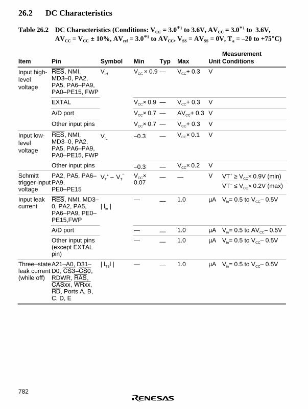
782
26.2 DC Characteristics
Table 26.2 DC Characteristics (Conditions: VCC = 3.0* 1 to 3.6V, AVCC = 3.0* 1 to 3.6V,AVCC = VCC ± 10%, AVref = 3.0* 1 to AVCC, VSS = AVSS = 0V, Ta = –20 to +75°C)
Item Pin Symbol Min Typ Max UnitMeasurementConditions
Input high-levelvoltage
RES, NMI,MD3–0, PA2,PA5, PA6–PA9,PA0–PE15, FWP
VIH VCC × 0.9 — VCC+ 0.3 V
EXTAL VCC× 0.9 — VCC+ 0.3 V
A/D port VCC× 0.7 — AVCC+ 0.3 V
Other input pins VCC× 0.7 — VCC+ 0.3 V
Input low-levelvoltage
RES, NMI,MD3–0, PA2,PA5, PA6–PA9,PA0–PE15, FWP
VIL –0.3 — VCC× 0.1 V
Other input pins –0.3 — VCC× 0.2 V
Schmitttrigger inputvoltage
PA2, PA5, PA6–PA9,PE0–PE15
VT+ – VT
– VCC×0.07
— — V VT+ ≥ VCC× 0.9V (min)
VT– ≤ VCC× 0.2V (max)
Input leakcurrent
RES, NMI, MD3–0, PA2, PA5,PA6–PA9, PE0–PE15,FWP
| lin |— — 1.0 µA Vin= 0.5 to VCC– 0.5V
A/D port — — 1.0 µA Vin= 0.5 to AVCC– 0.5V
Other input pins(except EXTALpin)
— — 1.0 µA Vin= 0.5 to VCC– 0.5V
Three–stateleak current(while off)
A21–A0, D31–D0, CS3–CS0,RDWR, RAS,CASxx, WRxx,RD, Ports A, B,C, D, E
| lTSl | — — 1.0 µA Vin= 0.5 to VCC– 0.5V
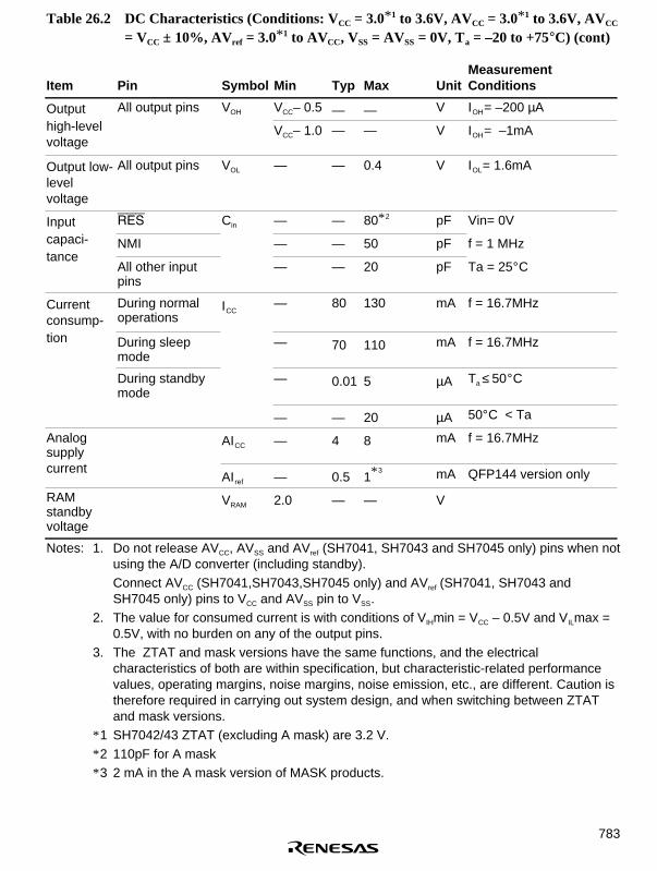
783
Table 26.2 DC Characteristics (Conditions: VCC = 3.0* 1 to 3.6V, AVCC = 3.0* 1 to 3.6V, AVCC
= VCC ± 10%, AVref = 3.0* 1 to AVCC, VSS = AVSS = 0V, Ta = –20 to +75°C) (cont)
Item Pin Symbol Min Typ Max UnitMeasurementConditions
Output All output pins VOH VCC– 0.5 — — V IOH= –200 µAhigh-levelvoltage
VCC– 1.0 — — V IOH= –1mA
Output low-levelvoltage
All output pins VOL — — 0.4 V IOL= 1.6mA
Input RES Cin — — 80* 2 pF Vin= 0Vcapaci- NMI — — 50 pF f = 1 MHztance
All other inputpins
— — 20 pF Ta = 25°C
Currentconsump-
During normaloperations
ICC— 80 130 mA f = 16.7MHz
tion During sleepmode
— 70 110 mA f = 16.7MHz
During standbymode
— 0.01 5 µA Ta ≤ 50°C
— — 20 µA 50°C < Ta
Analogsupply
AICC — 4 8 mA f = 16.7MHz
currentAIref — 0.5 1* 3 mA QFP144 version only
RAMstandbyvoltage
VRAM 2.0 — — V
Notes: 1. Do not release AVCC, AVSS and AVref (SH7041, SH7043 and SH7045 only) pins when notusing the A/D converter (including standby).Connect AVCC (SH7041,SH7043,SH7045 only) and AVref (SH7041, SH7043 andSH7045 only) pins to VCC and AVSS pin to VSS.
2. The value for consumed current is with conditions of VIHmin = VCC – 0.5V and VILmax =0.5V, with no burden on any of the output pins.
3. The ZTAT and mask versions have the same functions, and the electricalcharacteristics of both are within specification, but characteristic-related performancevalues, operating margins, noise margins, noise emission, etc., are different. Caution istherefore required in carrying out system design, and when switching between ZTATand mask versions.
* 1 SH7042/43 ZTAT (excluding A mask) are 3.2 V.* 2 110pF for A mask* 3 2 mA in the A mask version of MASK products.

784
Table 26.3 Permitted Output Current Values (Conditions: VCC = 3.0* to 3.6V, AVCC = 3.0*
to 3.6V, AVCC = VCC ± 10%, AVref = 3.0* to AVCC, VSS = AVSS = 0V, Ta = –20 to+75°C)
Item Symbol Min Typ Max Unit
Output low-level permissible current (per pin) IOL — — 2.0 mA
Output low-level permissible current (total) ∑ IOL — — 80 mA
Output high-level permissible current (per pin) –IOH — — 2.0 mA
Output high-level permissible current (total) ∑ (–IOH) — — 25 mA
Notes: To assure LSI reliability, do not exceed the output values listed in this table.* SH7042/43 ZTAT (excluding A mask) are 3.2V.
26.3 AC Characteristics
26.3.1 Clock Timing
Table 26.4 Clock Timing (Conditions: VCC = 3.0* to 3.6V, AVCC = 3.0* to 3.6V, AVCC = VCC ±10%, AVref = 3.0* to AVCC, VSS = AVSS = 0V, Ta = –20 to +75°C)
Item Symbol Min Max Unit Figures
Operating frequency fOP 4 16.7 MHz 26.1
Clock cycle time tcyc 60 250 ns
Clock low-level pulse width tCL 10 — ns
Clock high-level pulse width tCH 10 — ns
Clock rise time tCR — 5 ns
Clock fall time tCF — 5 ns
EXTAL clock input frequency fEX 4 10 MHz 26.2
EXTAL clock input cycle time tEXcyc 100 250 ns
EXTAL clock low-level input pulse width tEXL 40 — ns
EXTAL clock high-level input pulse width tEXH 40 — ns
EXTAL clock input rise time tEXR — 5 ns
EXTAL clock input fall time tEXF — 5 ns
Reset oscillation settling time tOSC1 10 — ms 26.3
Standby return clock settling time tOSC2 10 — ms
Note: * SH7042/43 ZTAT (excluding A mask) are 3.2V.

785
tcyc
tCLtCH
1/2VCC 1/2VCC
tCF tCR
CK
Figure 26.1 System Clock Timing
tEXcyc
tEXLtEXH
VIH VIH1/2VCC VIL VIL
1/2VCC
tEXF tEXR
EXTAL VIH
Figure 26.2 EXTAL Clock Input Timing
tOSC1
VCC min
tOSC2
CK
VCC
RES
Figure 26.3 Oscillation Settling Time

786
26.3.2 Control Signal Timing
Table 26.5 Control Signal Timing (Conditions: VCC = 3.0* 1 to 3.6V, AVCC = 3.0* 1 to 3.6V,AVCC = VCC ± 10%, AVref = 3.0* 1 to AVCC, VSS = AVSS = 0V, Ta = –20 to +75°C)
Item Symbol Min Max Unit Figure
RES rise/fall tRESr, tRESf — 200 ns 26.4
RES pulse width tRESW 20 — tcyc
MRES pulse width tMRESW 20 — tcyc
NMI rise/fall tNMIr, tNMIf — 200 ns 26.5
RES setup time* 1 tRESS 100 — ns 26.4
MRES setup time* 1 tMRESS 100 — ns 26.5
NMI setup time (during edge detection) tNMIS 100 — ns
IRQ7–IRQ0 setup time (edge detection)* 2 tIRQES 100 — ns
IRQ7–IRQ0 setup time (level detection)* 2 tIRQLS 100 — ns
NMI hold time tNMIH 50 — ns 26.5
IRQ7–IRQ0 hold time tIRQEH 50 — ns
IRQOUT output delay time tIRQOD — 50 ns 26.6
Bus request setup time tBRQS 35 — ns 26.7
Bus acknowledge delay time 1 tBACKD1 — 35 ns
Bus acknowledge delay time 2 tBACKD2 — 35 ns
Bus three state delay time tBZD — 35 ns
Notes: * 1 SH7042/43 ZTAT (excluding A mask) are 3.2V.* 2 The RES, MRES, NMI, BREQ, and IRQ7–IRQ0 signals are asynchronous inputs, but
when the setup times shown here are provided, the signals are considered to haveproduced changes at clock rise (for RES, MRES, BREQ) or clock fall (for NMI andIRQ7–IRQ0). If the setup times are not provided, recognition is delayed until the nextclock rise or fall.

787
CK
RES
MRES
tRESf
tRESW
tMRESW
tRESr
tRESS
tMRESS tMRESS
tRESS
VIH VIH
VIH
VIL VIL
VIL VIL
Figure 26.4 Reset Input Timing
tNMIH tNMIS
tNMIr,tNMIf
VIH
VIL
tIRQEH tIRQES
VIH
VIL
tIRQLS
CK
NMI
IRQ edge
IRQ level
Figure 26.5 Interrupt Signal Input Timing

788
tIRQODtIRQOD
CK
IRQOUT
Figure 26.6 Interrupt Signal Output Timing
CK
RD, RDWR, RAS, CASxx,
CSn, WRxx
A21–A0,D31–D0
tBRQStBRQS
tBACKD1 tBACKD2
tBZD
tBZD
BREQ (Input)
Note: During the bus-release period of a self-refresh, RAS, CASx, and RDWR are output.
BACK (Output)
Figure 26.7 Bus Right Release Timing

789
26.3.3 Bus Timing
Table 26.6 Bus Timing (Conditions: VCC = 3.0* 1 to 3.6V, AVCC = 3.0* 1 to 3.6V, AVCC = VCC
± 10%, AVref = 3.0* 1 to AVCC, VSS = AVSS = 0V, Ta = –20 to +75°C)
Item Symbol Min Max Unit Figure
Address delay time tAD 3* 4 35 ns 26.8, 9, 11–16, 19
CS delay time 1 tCSD1 3* 4 35 ns 26.8, 9, 19
CS delay time 2 tCSD2 3* 4 35 ns
Read strobe delay time 1 tRSD1 3* 4 35 ns 26.8, 9, 11–16, 19
Read strobe delay time 2 tRSD2 3* 4 35 ns
Read data setup time tRDS* 5 25 — ns
Read data hold time tRDH 0 — ns
Write strobe delay time 1 tWSD1 3* 4 35 ns
Write strobe delay time 2 tWSD2 3* 5 35 ns
Write data delay time tWDD — 45 ns
Write data hold time tWDH 0 25* 3 ns
WAIT setup time tWTS 15 — ns 26.10,15, 19
WAIT hold time tWTH 0 — ns
RAS delay time 1 tRASD1 3* 4 35 ns 26.11–18
RAS delay time 2 tRASD2 3* 4 35 ns
CAS delay time 1 tCASD1 3* 4 35 ns
CAS delay time 2 tCASD2 3* 4 35 ns
Read data access time tACC* 2 tcyc× (n+2) – 45 — ns 26.8, 9
Access time from read strobe tOE* 2 tcyc× (n+1.5) – 40 — ns
Access time from columnaddress
tAA* 2 tcyc× (n+2) – 45 — ns 26.11–16
Access time from RAS tRAC* 2 tcyc× (n+RCD+2.5) – 40 — ns
Access time from CAS tCAC* 2 tcyc× (n+1) – 40 — ns
Row address hold time tRAH tcyc× (RCD+0.5) – 15 — ns
Row address setup time tASR 0 — ns
Data input setup time tDS tcyc× (m+0.5) – 27 — ns
Data input hold time tDH 20 — ns
Notes: n is the wait number. m is 1 unless the DRAM write cycle wait number is 0, then m is 0.RCD is the set value of the RCD bit of DCR.* 1 SH7042/43 ZTAT (excluding A mask) are 3.2V.* 2 If the access time is satisfied, then the tRDS need not be satisfied.* 3 tWDH (max) is a reference value.* 4 The delay time min values are reference values (typ).* 5 tRDS is a reference value.
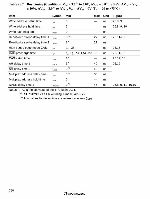
790
Table 26.7 Bus Timing (Conditions: VCC = 3.0* 1 to 3.6V, AVCC = 3.0* 1 to 3.6V, AVCC = VCC
± 10%, AVref = 3.0* 1 to AVCC, VSS = AVSS = 0V, Ta = –20 to +75°C)
Item Symbol Min Max Unit Figure
Write address setup time tAS 0 — ns 26.8, 9
Write address hold time tWR 5 — ns 26.8, 9, 19
Write data hold time tWRH 0 — ns
Read/write strobe delay time 1 tRWD1 3* 2 27 ns 26.11–16
Read/write strobe delay time 2 tRWD2 3* 2 27 ns
High-speed page mode CAS tCP tcyc–35 — ns 26.16
RAS precharge time tRP tcyc× (TPC+1.5) –20 — ns 26.11–16
CAS setup time tCSR 10 — ns 26.17, 18
AH delay time 1 tAHD1 3* 2 40 ns 26.19
AH delay time 2 tAHD2 3* 2 40 ns
Multiplex address delay time tMAD 3* 2 35 ns
Multiplex address hold time tMAH 0 — ns
DACK delay time 1 tDACKD1 3* 2 45 ns 26.8, 9, 11–16,19
Notes: TPC is the set value of the TPC bit in DCR.* 1 SH7042/43 ZTAT (excluding A mask) are 3.2V* 2 Min values for delay time are reference values (typ)

791
T1 T2
CK
A21–A0
DACKn
tDACKD1 tDACKD1
tWDHtWDD
tWSD1 tWSD2
tACCtRDS tRDH
tRSD1 tOE tRSD2
tCSD2tCSD1
tAD
tAS
tWR
tWRH
CSn
Note: tRDH is specified from fastest negate timing of A21–A0, CSn, and RD.
(During read)
(During read)
RD
D31–D0
D31–D0
WRxx(During write)
(During write)
Figure 26.8 Basic Cycle (No Waits)

792
CK
A21–A0
DACKn
T1 Tw T2
tAD
tCSD1
tRSD1
tWSD1
tWDD
tDACKD1
tRSD2
tCSD2
tRDS tRDH
tWSD2
tWDH
tDACKD1
tOE
tACC
tAStWRH
tWR
Note: tRDH is specified from fastest negate timing of A21–A0, CSn, and RD.
CSn
RD
D31–D0
D31–D0
(During read)
(During read)
(During write)
(During write)WRxx
Figure 26.9 Basic Cycle (Software Waits)

793
CK
A21–A0
T1 Tw TwoTw T2
tWTS tWTH tWTS tWTH
CSn
RD
WRxx
WAIT
DACKn
(During read)
(During read)
(During write)
(During write)
D31–D0
D31–D0
Figure 26.10 Basic Cycle (2 Software Waits + Wait due to WAIT Signal)

794
Tp Tr Tc1 Tc2
tAD tAD
tASR
tRP
tRASD1tRAH
tCASD1
tCAC
tAA
tRAC
tRDS
tRASD2
tCASD2
tRDH
tRWD1
tCASD2tCASD1
tRWD2
tWDH
tDHtDS
tWDD
tDACKD1tDACKD1
tRSD1 tRSD2
tWSD1 tWSD2
CK
A21–A0
RAS
CASxx
RDWR
D31– D0
D31–D0
CASxx
RDWR
DACKn
RD
WRxx
Note: tRDH is specified from fastest negate timing of A21–A0, RAS, and CAS.
(During read)
(During read)
(During read)
(During read)
(During write)
(During write)
(During write)
(During write)
Row address Column address
Figure 26.11 DRAM Cycle (Normal Mode, No Wait, TPC = 0, RCD = 0)

795
Tp
CK
A21–A0
Tr Tc1 Tcw1 Tc2
tAD tAD
tRP
tRASD1tASR
tCASD1
tRAH tRASD2
tCASD2
tCAC
tRAC
tAAtRDS tRDH
tCASD2
tRWD2
tWDH
tDHtDS
tWDD
tDACKD1tDACKD1
tRSD1
tWSD1 tWSD2
tRSD2
tCASD1
tRWD1
Row address Column address
RAS
CASxx
RDWR
D31–D0
CASxx
RDWR
D31–D0
DACKn
RD
WRxx
Note: tRDH is specified from fastest negate timing of A21–A0, RAS, and CAS.
(During read)
(During read)
(During read)
(During read)
(During write)
(During write)
(During write)
(During write)
Figure 26.12 DRAM Cycle (Normal Mode, 1 Wait, TPC = 0, RCD = 0)

796
CK
A21–A0
Tp Tpw Tr Trw Tc1 Tcw1 Tcw2 Tc2
tAD tAD
tASR
tRASD1tRAH
tRP
tCASD1
tCAC
tAAtRAC
tRDS tRDH
tCASD2tCASD1
tRWD2tRWD1
tDHtDS
tWDH
tDACKD1tDACKD1
tWDD
tRSD1 tRSD2
tWSD1 tWSD2
tRASD2
tCASD2
RAS
CASxx
RDWR
D31–D0
CASxx
RDWR
D31–D0
DACKn
RD
WRxx
(During read)
(During read)
(During read)
(During read)
(During write)
(During write)
(During write)
(During write)
Row address Column address
Note: tRDH is specified from fastest negate timing of A21–A0, RAS, and CAS.
Figure 26.13 DRAM Cycle (Normal Mode, 2 Waits, TPC = 1, RCD = 1)
CK
A21–A0
Tp Tpw Tr Trw Tc1 Tcw1 Tcw2 Tcw3 Tc2
tAD tAD
tRAHtASR
tRP
tCASD1
tCAC
tAA
tCASD1
tRDS
tCASD2
tRWD2tRWD1
tDS tDHtWDH
tDACKD1
tRSD1
tWSD1tWSD2
tRSD2
tDACKD1
tRASD2
tCASD2
tWDD
RAS
CASxx
RDWR
D31–D0
CASxx
RDWR
D31–D0
DACKn
RD
WRxx
(During read)
(During read)
(During read)
(During read)
(During write)
(During write)
(During write)
(During write)
Row address Column addresstRASD1
tRDH
tRAC
Note: tRDH is specified from fastest negate timing of A21–A0, RAS, and CAS.
Figure 26.14 DRAM Cycle (Normal Mode, 3 Waits, TPC = 1, RCD = 1)

797
CK
A21–A0
Tp Tr Tc1 Tcw1 Tcw2 Tcwo Tc2
tAD tAD
tASRtRAH
tRASD1
tRP
tCASD1
tCAC
tAA
tRAC
tRDH
tCASD2
tRWD2
tCASD1
tWDH
tDHtDS
tRWD1
tWDD
tWTS tWTH tWTS tWTH
tDACKD1
tRSD2
tWSD2tWSD1
tRSD1
tRASD2
tDACKD1
tCASD2
tRDS
RAS
CASxx
RDWR
D31–D0
CASxx
RDWR
D31–D0
DACKn
RD
WRxx
WAIT
(During read)
(During read)
(During read)
(During read)
(During write)
(During write)
(During write)
(During write)
Row address Column address
Note: tRDH is specified from fastest negate timing of A21–A0, RAS, and CAS.
Figure 26.15 DRAM Cycle (Normal Mode, 2 Waits + Wait due to WAIT Signal)
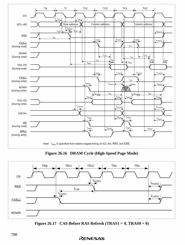
798
CK
A21–A0
Tp Tr Tc1 Tc2 Tc1 Tc2
tAD tAD
tASR
tRASD1tRAH
tRPtCASD1 tCASD2 tCASD1 tCASD2
tRASD2
tCP
tAA
tCAC
tAAtRAC
tRDStRDH
tRDS tRDH
tCAC
tCASD1tCASD2tCASD1 tCASD2
tRWD2tRWD1tRWD2tRWD1
tDHtDS
tWDD tWDH tWDD tWDH
tDHtDS
tCP
tDACKD1 tDACKD1
tRSD1
tWSD1 tWSD2tWSD1 tWSD2
tRSD2 tRSD1 tRSD2
tDACKD1
RAS
CASxx
RDWR
D31–D0
CASxx
RDWR
D31–D0
DACKn
RD
WRxx
(During read)
(During read)
(During read)
(During read)
(During write)
(During write)
(During write)
(During write)
Note: tRDH is specified from fastest negate timing of A21–A0, RAS, and CAS.
Row address Column address Column address
Figure 26.16 DRAM Cycle (High-Speed Page Mode)
CK
RDWR
TRp TRr1 TRr2 TRc TRc
tRASD1tRASD2
tCASD2
tCSR
tCASD1
RAS
CASxx
Figure 26.17 CAS Before RAS Refresh (TRAS1 = 0, TRAS0 = 0)

799
CK
RAS
CASxx
RDWR
TRcc
tRASD2
tCASD2
tCSR
tCASD1
TRp TRr1 TRr2
tRASD1
TRc
Figure 26.18 Self Refresh
CK
A21–A0
DACKn
Ta1 Ta2 Ta3 Ta4 T1 TW TWo T2
tAD
tCSD1 tCSD2
tAHD1 tAHD2
tRSD2
tMAHtMAD tRDS tRDH
tMAH tWDDtMAD tWDH
tDACKD1tDACKD1
tWTS tWTH tWTS tWTH
tWSD2
tRSD1
CS3
AH
D15–D0
WAIT
D15–D0
RD
WRxx
(During read)
Address
Address
(During read)
(During write)
(During write)
tWSD1
Note: tRDH is specified from fastest negate timing of A21–A0, CS3, and RD.
tWR
tWRH
Figure 26.19 Address Data Multiplex I/O Space Cycle (1 Software Wait + External Wait)

800
26.3.4 Direct Memory Access Controller Timing
Table 26.8 Direct Memory Access Controller Timing (Conditions: VCC = 3.0* to 3.6V, AVCC
= 3.0* to 3.6V, AVCC = VCC ± 10%, AVref = 3.0* to AVCC, VSS = AVSS = 0V, Ta =–20 to +75°C)
Item Symbol Min Max Unit Figure
DREQ0, DREQ1 setup time tDRQS 35 — ns 26.20
DREQ0, DREQ1 hold time tDRQH 35 — ns
DREQ0, DREQ1 pulse width tDRQW 1.5 — tcyc 26.21
DRAK output delay time tDRAKD — 35 ns 26.22
Note: * SH7042/43 ZTAT (excluding A mask) are 3.2V.
CK
tDRQS
tDRQS
tDRQS
tDRQH
DREQ0DREQ1
Level clear
DREQ0DREQ1
Level
DREQ0DREQ1
Edge
Figure 26.20 DREQ0 and DREQ1 Input Timing (1)

801
CK
tDRQW
DREQ0DREQ1
Edge
Figure 26.21 DREQ0 and DREQ1 Input Timing (2)
CK
tDRAKD tDRAKD
DRAKn
Figure 26.22 DRAK Output Delay Time

802
26.3.5 Multifunction Timer Pulse Unit Timing
Table 26.9 Multifunction Timer Pulse Unit Timing (Conditions:VCC = 3.0* to 3.6V, AVCC =3.0* to 3.6V, AVCC = VCC ± 10%, AVref = 3.0* to AVCC, VSS = AVSS = 0V, Ta =–20 to +75°C)
Item Symbol Min Max Unit Figure
Output compare output delay time tTOCD — 100 ns 26.23
Input capture input setup time tTICS 100 — ns
Timer input setup time tTCKS 100 — ns 26.24
Timer clock pulse width (single edgespecification)
tTCKWH/L 1.5 — tcyc
Timer clock pulse width (both edgesspecified)
tTCKWH/L 2.5 — tcyc
Timer clock pulse width (phasemeasurement mode)
tTCKWH/L 2.5 — tcyc
Note: * SH7042/43 ZTAT (excluding A mask) are 3.2V.
CK
tTOCD
tTICS
Input capture input
Output compare output
Figure 26.23 MTU I/O Timing
CK
TCLKA to TCLKD
tTCKS tTCKS
tTCKWHtTCKWL
Figure 26.24 MTU Clock Input Timing

803
26.3.6 I/O Port Timing
Table 26.10 I/O Port Timing (Conditions:VCC = 3.0* to 3.6V, AVCC = 3.0* to 3.6V, AVCC =VCC ± 10%, AVref = 3.0* to AVCC, VSS = AVSS = 0V, Ta = –20 to +75°C)
Item Symbol Min Max Unit Figure
Port output data delay time tPWD — 100 ns 26.25
Port input hold time tPRH 100 — ns
Port input setup time tPRS 100 — ns
Note: * SH7042/43 ZTAT (excluding A mask) are 3.2V.
tPRS tPRH
tPWD
T1 T2
CK
Port (Read)
Port (Write)
Figure 26.25 I/O Port I/O Timing

804
26.3.7 Watchdog Timer Timing
Table 26.11 Watchdog Timer Timing (Conditions:VCC = 3.0* to 3.6V, AVCC = 3.0* to 3.6V,AVCC = VCC ± 10%, AVref = 3.0* to AVCC, VSS = AVSS = 0V, Ta = –20 to +75°C)
Item Symbol Min Max Unit Figure
WDTOVF delay time tWOVD — 100 ns 26.26
Note: * SH7042/43 ZTAT (excluding A mask) are 3.2V.
CK
tWOVD
WDTOVF
tWOVD
Figure 26.26 Watchdog Timer Timing

805
26.3.8 Serial Communication Interface Timing
Table 26.12 Serial Communication Interface Timing (Conditions:VCC = 3.0* to 3.6V, AVCC =3.0* to 3.6V, AVCC = VCC ± 10%, AVref = 3.0* to AVCC, VSS = AVSS = 0V, Ta = –20to +75°C)
Item Symbol Min Max Unit Figure
Input clock cycle tscyc 4 — tcyc 26.27
Input clock cycle (clock sync) tscyc 6 — tcyc
Input clock pulse width tsckw 0.5 0.6 tscyc
Input clock rise time tsckr — 1.5 tcyc
Input clock fall time tsckf — 1.5 tcyc
Transmit data delay time (clock sync) tTXD — 100 ns 26.28
Receive data setup time (clock sync) tRXS 100 — ns
Receive data hold time (clock sync) tRXH 100 — ns
Note: * SH7042/43 ZTAT (excluding A mask) are 3.2V.
tsckw tsckr tsckf
tscyc
SCK0, SCK1
Figure 26.27 Input Clock Timing
tscyc
tTXD
tRXS tRXH
SCK0, SCK1
TXD0, TXD1(Transmit data)
RXD0, RXD1(Receive data)
Figure 26.28 SCI I/O Timing (Clock Sync Mode)
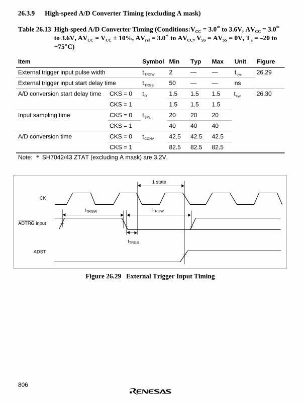
806
26.3.9 High-speed A/D Converter Timing (excluding A mask)
Table 26.13 High-speed A/D Converter Timing (Conditions:VCC = 3.0* to 3.6V, AVCC = 3.0*
to 3.6V, AVCC = VCC ± 10%, AVref = 3.0* to AVCC, VSS = AVSS = 0V, Ta = –20 to+75°C)
Item Symbol Min Typ Max Unit Figure
External trigger input pulse width tTRGW 2 — — tcyc 26.29
External trigger input start delay time tTRGS 50 — — ns
A/D conversion start delay time CKS = 0 tD 1.5 1.5 1.5 tcyc 26.30
CKS = 1 1.5 1.5 1.5
Input sampling time CKS = 0 tSPL 20 20 20
CKS = 1 40 40 40
A/D conversion time CKS = 0 tCONV 42.5 42.5 42.5
CKS = 1 82.5 82.5 82.5
Note: * SH7042/43 ZTAT (excluding A mask) are 3.2V.
tTRGS
CK
ADST
ADTRG input
tTRGWtTRGW
1 state
Figure 26.29 External Trigger Input Timing

807
ADF
tD
tDtSPLtCONVtCP
tSPL tCP
tCONV
ADST
: A/D conversion start delay time: Input sampling time: A/D conversion time: Operation time
Address
Write signal
Sampling timing
φ
Figure 26.30 Analog Conversion Timing
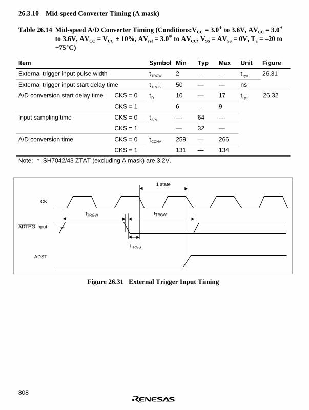
808
26.3.10 Mid-speed Converter Timing (A mask)
Table 26.14 Mid-speed A/D Converter Timing (Conditions:VCC = 3.0* to 3.6V, AVCC = 3.0*
to 3.6V, AVCC = VCC ± 10%, AVref = 3.0* to AVCC, VSS = AVSS = 0V, Ta = –20 to+75°C)
Item Symbol Min Typ Max Unit Figure
External trigger input pulse width tTRGW 2 — — tcyc 26.31
External trigger input start delay time tTRGS 50 — — ns
A/D conversion start delay time CKS = 0 tD 10 — 17 tcyc 26.32
CKS = 1 6 — 9
Input sampling time CKS = 0 tSPL — 64 —
CKS = 1 — 32 —
A/D conversion time CKS = 0 tCONV 259 — 266
CKS = 1 131 — 134
Note: * SH7042/43 ZTAT (excluding A mask) are 3.2V.
tTRGS
CK
ADST
tTRGWtTRGW
ADTRG input
1 state
Figure 26.31 External Trigger Input Timing

809
ADF
t D t SPL
t CONV
t D
t SPL
t CONV
: ADCSR write cycle: ADCSR address: A/D conversion start delay time: Input sampling time: A/D conversion time
Address
Write signal
Input sampling timing
CK
(1)
(2)
Legend:
(1)(2)
Figure 26.32 Analog Conversion Timing

810
26.3.11 Measurement Conditions for AC Characteristic
• Input reference levels:
High level: 2.2 V
Low level: 0.8 V
• Output reference levels:
High level: 2.0 V
Low level: 0.8 V
IOL
VrefCL
IOH
V
LSI output pin DUT output
CL is set with the following pins, including the total capacitance of the measurement equipment etc:
Note:
30 pF:
50 pF:70 pF:
IOL, IOH:
CK, RAS, CASxx, RDWR, CS0–CS3, AH, BREQ, BACK, DACK0, DACK1, and IRQOUT A21–A0, D31–D0, RD, WRxxPort output and peripheral module output pins other than the above.See table 26.3, Permitted Output Current Values.
Figure 26.33 Output Load Circuit

811
26.4 A/D Converter Characteristics
Table 26.15 A/D Converter Characteristics (excluding A mask) (Conditions:VCC = 3.0* 1 to3.6V, AVCC = 3.0* 1 to 3.6V, AVCC = VCC ± 10%, AVref = 3.0* 1 to AVCC, VSS =AVSS = 0V, Ta = –20 to +75°C)
16.7MHz
Item Min Typ Max Unit
Resolution 10 10 10 bit
Conversion time (when CKS = 1) — — 5 µs
Analog input capacity — — 20 pF
Permission signal source impedance — — 1 kΩ
Non-linearity error* 2 — — ± 15 LSB
Offset error* 2 — — ± 15 LSB
Full scale error* 2 — — ± 15 LSB
Quantize error* 2 — — ± 0.5 LSB
Absolute error — — ± 31 LSB
Notes: * 1 SH7042/43 ZTAT (excluding A mask) are 3.2V.* 2 Reference values
Table 26.16 A/D Converter Characteristics (A mask) (Conditions:VCC = 3.0* 1 to 3.6V, AVCC
= 3.0* 1 to 3.6V, AVCC = VCC ± 10%, AVref = 3.0* 1 to AVCC, VSS = AVSS = 0V, Ta =–20 to +75°C)
16.7MHz
Item min typ max Unit
Resolution 10 10 10 bit
Conversion time (when CKS = 0) — — 16.0 µs
Analog input capacity — — 20 pF
Permission signal source impedance — — 1 kΩ
Non-linearity error* 2 — — ±4 LSB
Offset error* 2 — — ±4 LSB
Full scale error* 2 — — ±4 LSB
Quantize error* 2 — — ±0.5 LSB
Absolute error — — ±6 LSB
Notes: * 1 SH7042/43 ZTAT (excluding A mask) are 3.2V.* 2 Reference values

812

813
Appendix A On-Chip Supporting Module Registers
A.1 Addresses
Table A.1 On-Chip I/O Register Addresses
Register Bit Names
Address Abbr. Bit 7 Bit 6 Bit 5 Bit 4 Bit 3 Bit 2 Bit 1 Bit 0 Module
— DTMR SM1 SM0 DM1 DM0 MD1 MD0 SZ1 SZ0 DTC
DTS CHNE DISEL NMIM — — — —
— DTSAR
— DTDAR
— DTIAR
— DTCRA
— DTCRB
H'FFFF81A0 SMR0 C/A CHR PE O/E STOP MP CKS1 CKS0 SCI
H'FFFF81A1 BRR0
H'FFFF81A2 SCR0 TIE RIE TE RE MPIE TEIE CKE1 CKE0
H'FFFF81A3 TDR0
H'FFFF81A4 SSR0 TDRE RDRF ORER FER PER TEND MPB MPBT
H'FFFF81A5 RDR0
H'FFFF81A6toH'FFFF81AF
— — — — — — — — —

814
Table A.1 On-Chip I/O Register Addresses (cont)
Register Bit Names
Address Abbr. Bit 7 Bit 6 Bit 5 Bit 4 Bit 3 Bit 2 Bit 1 Bit 0 Module
H'FFFF81B0 SMR1 C/A CHR PE O/E STOP MP CKS1 CKS0 SCI
H'FFFF81B1 BRR1
H'FFFF81B2 SCR1 TIE RIE TE RE MPIE TEIE CKE1 CKE0
H'FFFF81B3 TDR1
H'FFFF81B4 SSR1 TDRE RDRF ORER FER PER TEND MPB MPBT
H'FFFF81B5 RDR1
H'FFFF81B6toH'FFFF81FF
— — — — — — — — —
H'FFFF8200 TCR3 CCLR2 CCLR1 CCLR0 CKEG1 CKEG0 TPSC2 TPSC1 TPSC0 MTU
H'FFFF8201 TCR4 CCLR2 CCLR1 CCLR0 CKEG1 CKEG0 TPSC2 TPSC1 TPSC0
H'FFFF8202 TMDR3 — — BFB BFA MD3 MD2 MD1 MD0
H'FFFF8203 TMDR4 — — BFB BFA MD3 MD2 MD1 MD0
H'FFFF8204 TIOR3H IOB3 IOB2 IOB1 IOB0 IOA3 IOA2 IOA1 IOA0
H'FFFF8205 TIOR3L IOD3 IOD2 IOD1 IOD0 IOC3 IOC2 IOC1 IOC0
H'FFFF8206 TIOR4H IOB3 IOB2 IOB1 IOB0 IOA3 IOA2 IOA1 IOA0
H'FFFF8207 TIOR4L IOD3 IOD2 IOD1 IOD0 IOC3 IOC2 IOC1 IOC0
H'FFFF8208 TIER3 TTGE — — TCIEV TGIED TGIEC TGIEB TGIEA
H'FFFF8209 TIER4 TTGE — — TCIEV TGIED TGIEC TGIEB TGIEA
H'FFFF820A TOER — — OE4D OE4C OE3D OE4B OE4A OE3B
H'FFFF820B TOCR — PSYE — — — — OLSN OLSP
H'FFFF820C — — — — — — — — —
H'FFFF820D TGCR — BDC N P FB WF VF UF
H'FFFF820E — — — — — — — — —
H'FFFF820F — — — — — — — — —
H'FFFF8210 TCNT3
H'FFFF8211
H'FFFF8212 TCNT4
H'FFFF8213
H'FFFF8214 TCDR
H'FFFF8215
H'FFFF8216 TDDR
H'FFFF8217
H'FFFF8218 TGR3A
H'FFFF8219

815
Table A.1 On-Chip I/O Register Addresses (cont)
Register Bit Names
Address Abbr. Bit 7 Bit 6 Bit 5 Bit 4 Bit 3 Bit 2 Bit 1 Bit 0 Module
H'FFFF821A TGR3B MTU
H'FFFF821B
H'FFFF821C TGR4A
H'FFFF821D
H'FFFF821E TGR4B
H'FFFF821F
H'FFFF8220 TCNTS
H'FFFF8221
H'FFFF8222 TCBR
H'FFFF8223
H'FFFF8224 TGR3C
H'FFFF8225
H'FFFF8226 TGR3D
H'FFFF8227
H'FFFF8228 TGR4C
H'FFFF8229
H'FFFF822A TGR4D
H'FFFF822B
H'FFFF822C TSR3 TCFD — — TCFV TGFD TGFC TGFB TGFA
H'FFFF822D TSR4 TCFD — — TCFV TGFD TGFC TGFB TGFA
H'FFFF822E — — — — — — — — —
H'FFFF822F — — — — — — — — —
H'FFFF8230toH'FFFF823F
— — — — — — — — —
H'FFFF8240 TSTR CST4 CST3 — — — CST2 CST1 CST0
H'FFFF8241 TSYR SYNC4 SYNC3 — — — SYNC2 SYNC1 SYNC0
H'FFFF8242toH'FFFF825F
— — — — — — — — —
H'FFFF8260 TCR0 CCLR2 CCLR1 CCLR0 CKEG1 CKEG0 TPSC2 TPSC1 TPSC0
H'FFFF8261 TMDR0 — — BFB BFA MD3 MD2 MD1 MD0
H'FFFF8262 TIOR0H IOB3 IOB2 IOB1 IOB0 IOA3 IOA2 IOA1 IOA0
H'FFFF8263 TIOR0L IOD3 IOD2 IOD1 IOD0 IOC3 IOC2 IOC1 IOC0
H'FFFF8264 TIER0 TTGE — — TCIEV TGIED TGIEC TGIEB TGIEA
H'FFFF8265 TSR0 — — — TCFV TGFD TGFC TGFB TGFA
H'FFFF8266 TCNT0
H'FFFF8267

816
Table A.1 On-Chip I/O Register Addresses (cont)
Register Bit Names
Address Abbr. Bit 7 Bit 6 Bit 5 Bit 4 Bit 3 Bit 2 Bit 1 Bit 0 Module
H'FFFF8268 TGR0A MTU
H'FFFF8269
H'FFFF826A TGR0B
H'FFFF826B
H'FFFF826C TGR0C
H'FFFF826D
H'FFFF826E TGR0D
H'FFFF826F
H'FFFF8270toH'FFFF827F
— — — — — — — — —
H'FFFF8280 TCR1 — CCLR1 CCLR0 CKEG1 CKEG0 TPSC2 TPSC1 TPSC0
H'FFFF8281 TMDR1 — — — — MD3 MD2 MD1 MD0
H'FFFF8282 TIOR1 IOB3 IOB2 IOB1 IOB0 IOA3 IOA2 IOA1 IOA0
H'FFFF8283 — — — — — — — — —
H'FFFF8284 TIER1 TTGE — TCIEU TCIEV — — TGIEB TGIEA
H'FFFF8285 TSR1 TCFD — TCFU TCFV — — TGFB TGFA
H'FFFF8286 TCNT1
H'FFFF8287
H'FFFF8288 TGR1A
H'FFFF8289
H'FFFF828A TGR1B
H'FFFF828B
H'FFFF828CtoH'FFFF829F
— — — — — — — — —
H'FFFF82A0 TCR2 — CCLR1 CCLR0 CKEG1 CKEG0 TPSC2 TPSC1 TPSC0
H'FFFF82A1 TMDR2 — — — — MD3 MD2 MD1 MD0
H'FFFF82A2 TIOR2 IOB3 IOB2 IOB1 IOB0 IOA3 IOA2 IOA1 IOA0
H'FFFF82A3 — — — — — — — — —
H'FFFF82A4 TIER2 TTGE — TCIEU TCIEV — — TGIEB TGIEA
H'FFFF82A5 TSR2 TCFD — TCFU TCFV — — TGFB TGFA
H'FFFF82A6 TCNT2
H'FFFF82A7
H'FFFF82A8 TGR2A
H'FFFF82A9
H'FFFF82AA TGR2B
H'FFFF82AB

817
Table A.1 On-Chip I/O Register Addresses (cont)
Register Bit Names
Address Abbr. Bit 7 Bit 6 Bit 5 Bit 4 Bit 3 Bit 2 Bit 1 Bit 0 Module
H'FFFF82ACtoH'FFFF8347
— — — — — — — — — MTU
H'FFFF8348 IPRA INTC
H'FFFF8349
H'FFFF834A IPRB
H'FFFF834B
H'FFFF834C IPRC
H'FFFF834D
H'FFFF834E IPRD
H'FFFF834F
H'FFFF8350 IPRE
H'FFFF8351
H'FFFF8352 IPRF
H'FFFF8353
H'FFFF8354 IPRG
H'FFFF8355
H'FFFF8356 IPRH
H'FFFF8357
H'FFFF8358 ICR NMIL — — — — — — NMIE
H'FFFF8359 IRQ0S IRQ1S IRQ2S IRQ3S IRQ4S IRQ5S IRQ6S IRQ7S
H'FFFF835A ISR — — — — — — — —
H'FFFF835B IRQ0F IRQ1F IRQ2F IRQ3F IRQ4F IRQ5F IRQ6F IRQ7F
H'FFFF835CtoH'FFFF837F
— — — — — — — — —
H'FFFF8380 PADRH — — — — — — — — I/O
H'FFFF8381 PA23DR PA22DR PA21DR PA20DR PA19DR PA18DR PA17DR PA16DR
H'FFFF8382 PADRL PA15DR PA14DR PA13DR PA12DR PA11DR PA10DR PA9DR PA8DR
H'FFFF8383 PA7DR PA6DR PA5DR PA4DR PA3DR PA2DR PA1DR PA0DR
H'FFFF8384 PAIORH — — — — — — — — PFC
H'FFFF8385 PA23IOR PA22IOR PA21IOR PA20IOR PA19IOR PA18IOR PA17IOR PA16IOR
H'FFFF8386 PAIORL PA15IOR PA14IOR PA13IOR PA12IOR PA11IOR PA10IOR PA9IOR PA8IOR
H'FFFF8387 PA7IOR PA6IOR PA5IOR PA4IOR PA3IOR PA2IOR PA1IOR PA0IOR
H'FFFF8388 PACRH — PA23MD — PA22MD — PA21MD — PA20MD
H'FFFF8389 PA19MD1 PA19MD0 PA18MD1 PA18MD0 — PA17MD — PA16MD

818
Table A.1 On-Chip I/O Register Addresses (cont)
Register Bit Names
Address Abbr. Bit 7 Bit 6 Bit 5 Bit 4 Bit 3 Bit 2 Bit 1 Bit 0 Module
H'FFFF838A — — — — — — — — — PFC
H'FFFF838B — — — — — — — — —
H'FFFF838C PACRL1 — PA15MD — PA14MD — PA13MD — PA12MD
H'FFFF838D — PA11MD — PA10MD PA9MD1 PA9MD0 PA8MD1 PA8MD0
H'FFFF838E PACRL2 PA7MD1 PA7MD0 PA6MD1 PA6MD0 PA5MD1 PA5MD0 — PA4MD
H'FFFF838F — PA3MD PA2MD1 PA2MD0 — PA1MD — PA0MD
H'FFFF8390 PBDR — — — — — — PB9DR PB8DR I/O
H'FFFF8391 PB7DR PB6DR PB5DR PB4DR PB3DR PB2DR PB1DR PB0DR
H'FFFF8392 PCDR PC15DR PC14DR PC13DR PC12DR PC11DR PC10DR PC9DR PC8DR
H'FFFF8393 PC7DR PC6DR PC5DR PC4DR PC3DR PC2DR PC1DR PC0DR
H'FFFF8394 PBIOR — — — — — — PB9IOR PB8IOR PFC
H'FFFF8395 PB7IOR PB6IOR PB5IOR PB4IOR PB3IOR PB2IOR PB1IOR PB0IOR
H'FFFF8396 PCIOR PC15IOR PC14IOR PC13IOR PC12IOR PC11IOR PC10IOR PC9IOR PC8IOR
H'FFFF8397 PC7IOR PC6IOR PC5IOR PC4IOR PC3IOR PC2IOR PC1IOR PC0IOR
H'FFFF8398 PBCR1 — — — — — — — —
H'FFFF8399 — — — — PB9MD1 PB9MD0 PB8MD1 PB8MD0
H'FFFF839A PBCR2 PB7MD1 PB7MD0 PB6MD1 PB6MD0 PB5MD1 PB5MD0 PB4MD1 PB4MD0
H'FFFF839B PB3MD1 PB3MD0 PB2MD1 PB2MD0 — PB1MD — PB0MD
H'FFFF839C PCCR PC15MD PC14MD PC13MD PC12MD PC11MD PC10MD PC9MD PC8MD
H'FFFF839D PC7MD PC6MD PC5MD PC4MD PC3MD PC2MD PC1MD PC0MD
H'FFFF839E — — — — — — — — —
H'FFFF839F — — — — — — — — —
H'FFFF83A0 PDDRH PD31DR PD30DR PD29DR PD28DR PD27DR PD26DR PD25DR PD24DR I/O
H'FFFF83A1 PD23DR PD22DR PD21DR PD20DR PD19DR PD18DR PD17DR PD16DR
H'FFFF83A2 PDDRL PD15DR PD14DR PD13DR PD12DR PD11DR PD10DR PD9DR PD8DR
H'FFFF83A3 PD7DR PD6DR PD5DR PD4DR PD3DR PD2DR PD1DR PD0DR
H'FFFF83A4 PDIORH PD31IOR PD30IOR PD29IOR PD28IOR PD27IOR PD26IOR PD25IOR PD24IOR PFC
H'FFFF83A5 PD23IOR PD22IOR PD21IOR PD20IOR PD19IOR PD18IOR PD17IOR PD16IOR
H'FFFF83A6 PDIORL PD15IOR PD14IOR PD13IOR PD12IOR PD11IOR PD10IOR PD9IOR PD8IOR
H'FFFF83A7 PD7IOR PD6IOR PD5IOR PD4IOR PD3IOR PD2IOR PD1IOR PD0IOR
H'FFFF83A8 PDCRH1 PD31MD1 PD31MD0 PD30MD1 PD30MD0 PD29MD1 PD29MD0 PD28MD1 PD28MD0
H'FFFF83A9 PD27MD1 PD27MD0 PD26MD1 PD26MD0 PD25MD1 PD25MD0 PD24MD1 PD24MD0
H'FFFF83AA PDCRH2 PD23MD1 PD23MD0 PD22MD1 PD22MD0 PD21MD1 PD21MD0 PD20MD1 PD20MD0
H'FFFF83AB PD19MD1 PD19MD0 PD18MD1 PD18MD0 PD17MD1 PD17MD0 PD16MD1 PD16MD0

819
Table A.1 On-Chip I/O Register Addresses (cont)
Register Bit Names
Address Abbr. Bit 7 Bit 6 Bit 5 Bit 4 Bit 3 Bit 2 Bit 1 Bit 0 Module
H'FFFF83AC PDCRL PD15MD PD14MD PD13MD PD12MD PD11MD PD10MD PD9MD PD8MD PFC
H'FFFF83AD PD7MD PD6MD PD5MD PD4MD PD3MD PD2MD PD1MD PD0MD
H'FFFF83AE — — — — — — — — —
H'FFFF83AF — — — — — — — — —
H'FFFF83B0 PEDR PE15DR PE14DR PE13DR PE12DR PE11DR PE10DR PE9DR PE8DR I/O
H'FFFF83B1 PE7DR PE6DR PE5DR PE4DR PE3DR PE2DR PE1DR PE0DR
H'FFFF83B2 PFDR — — — — — — — —
H'FFFF83B3 PF7DR PF6DR PF5DR PF4DR PF3DR PF2DR PF1DR PF0DR
H'FFFF83B4 PEIOR PE15IOR PE14IOR PE13IOR PE12IOR PE11IOR PE10IOR PE9IOR PE8IOR PFC
H'FFFF83B5 PE7IOR PE6IOR PE5IOR PE4IOR PE3IOR PE2IOR PE1IOR PE0IOR
H'FFFF83B6 — — — — — — — — —
H'FFFF83B7 — — — — — — — — —
H'FFFF83B8 PECR1 PE15MD1 PE15MD0 PE14MD1 PE14MD0 PE13MD1 PE13MD0 — PE12MD
H'FFFF83B9 — PE11MD — PE10MD — PE9MD — PE8MD
H'FFFF83BA PECR2 — PE7MD — PE6MD — PE5MD — PE4MD
H'FFFF83BB PE3MD1 PE3MD0 PE2MD1 PE2MD0 PE1MD1 PE1MD0 PE0MD1 PE0MD0
H'FFFF83BCtoH'FFFF83BF
— — — — — — — — — —
H'FFFF83C0 ICSR POE3F POE2F POE1F POE0F — — — PIE MTU
H'FFFF83C1 POE3M1 POE3M0 POE2M1 POE2M0 POE1M1 POE1M0 POE0M1 POE0M0
H'FFFF83C2 OCSR OSF — — — — — OCE OIE
H'FFFF83C3 — — — — — — — —
H'FFFF83C4toH'FFFF83C7
— — — — — — — — — —
H'FFFF83C8 IFCR — — — — — — — — PFC
H'FFFF83C9 — — — — IRQMD3 IRQMD2 IRQMD1 IRQMD0
H'FFFF83CAtoH'FFFF83CF
— — — — — — — — — —
H'FFFF83D0 CMSTR — — — — — — — — CMT
H'FFFF83D1 — — — — — — STR1 STR0
H'FFFF83D2 CMCSR0 — — — — — — — —
H'FFFF83D3 CMF CMIE — — — — CKS1 CKS0
H'FFFF83D4 CMCNT0
H'FFFF83D5

820
Table A.1 On-Chip I/O Register Addresses (cont)
Register Bit Names
Address Abbr. Bit 7 Bit 6 Bit 5 Bit 4 Bit 3 Bit 2 Bit 1 Bit 0 Module
H'FFFF83D6 CMCOR0 CMT
H'FFFF83D7
H'FFFF83D8 CMCSR1 — — — — — — — —
H'FFFF83D9 CMF CMIE — — — — CKS1 CKS0
H'FFFF83DA CMCNT1
H'FFFF83DB
H'FFFF83DC CMCOR1
H'FFFF83DD
H'FFFF83DE — — — — — — — — —
H'FFFF83DF — — — — — — — — —
H'FFFF83E0 ADCSR ADF ADIE ADST CKS GRP CH2 CH1 CH0 A/D
H'FFFF83E1 ADCR — PWR TRGS1 TRGS0 SCAN DSMP BUFE1 BUFE0 (High
H'FFFF83E2toH'FFFF83EF
— — — — — — — — —speed)(Excl. Amask)
H'FFFF83F0 ADDRA — — — — — — AD9 AD8
H'FFFF83F1 AD7 AD6 AD5 AD4 AD3 AD2 AD1 AD0
H'FFFF83F2 ADDRB — — — — — — AD9 AD8
H'FFFF83F3 AD7 AD6 AD5 AD4 AD3 AD2 AD1 AD0
H'FFFF83F4 ADDRC — — — — — — AD9 AD8
H'FFFF83F5 AD7 AD6 AD5 AD4 AD3 AD2 AD1 AD0
H'FFFF83F6 ADDRD — — — — — — AD9 AD8
H'FFFF83F7 AD7 AD6 AD5 AD4 AD3 AD2 AD1 AD0
H'FFFF83F8 ADDRE — — — — — — AD9 AD8
H'FFFF83F9 AD7 AD6 AD5 AD4 AD3 AD2 AD1 AD0
H'FFFF83FA ADDRF — — — — — — AD9 AD8
H'FFFF83FB AD7 AD6 AD5 AD4 AD3 AD2 AD1 AD0
H'FFFF83FC ADDRG — — — — — — AD9 AD8
H'FFFF83FD AD7 AD6 AD5 AD4 AD3 AD2 AD1 AD0
H'FFFF83FE ADDRH — — — — — — AD9 AD8
H'FFFF83FF AD7 AD6 AD5 AD4 AD3 AD2 AD1 AD0
H'FFFF8400 ADDRA0 AD9 AD8 AD7 AD6 AD5 AD4 AD3 AD2 A/D(Mid-
H'FFFF8401 AD1 AD0 — — — — — — speed)
H'FFFF8402 ADDRB0 AD9 AD8 AD7 AD6 AD5 AD4 AD3 AD2 (A mask
H'FFFF8403 AD1 AD0 — — — — — — only)
H'FFFF8404 ADDRC0 AD9 AD8 AD7 AD6 AD5 AD4 AD3 AD2
H'FFFF8405 AD1 AD0 — — — — — —

821
Table A.1 On-Chip I/O Register Addresses (cont)
Register Bit Names
Address Abbr. Bit 7 Bit 6 Bit 5 Bit 4 Bit 3 Bit 2 Bit 1 Bit 0 Module
H'FFFF8406 ADDRD0 AD9 AD8 AD7 AD6 AD5 AD4 AD3 AD2 A/D(Mid-
H'FFFF8407 AD1 AD0 — — — — — — speed)
H'FFFF8408 ADDRA1 AD9 AD8 AD7 AD6 AD5 AD4 AD3 AD2 (A mask
H'FFFF8409 AD1 AD0 — — — — — — only)
H'FFFF840A ADDRB1 AD9 AD8 AD7 AD6 AD5 AD4 AD3 AD2
H'FFFF840B AD1 AD0 — — — — — —
H'FFFF840C ADDRC1 AD9 AD8 AD7 AD6 AD5 AD4 AD3 AD2
H'FFFF840D AD1 AD0 — — — — — —
H'FFFF840E ADDRD1 AD9 AD8 AD7 AD6 AD5 AD4 AD3 AD2
H'FFFF840F AD1 AD0 — — — — — —
H'FFFF8410 ADCSR0 ADF ADIE ADST SCAN CKS CH2 CH1 CH0
H'FFFF8411 ADCSR1 ADF ADIE ADST SCAN CKS CH2 CH1 CH0
H'FFFF8412 AADCR0 TRGE — — — — — — —
H'FFFF8413 AADCR1 TRGE — — — — — — —
H'FFFF8414toH'FFFF857F
— — — — — — — — —
H'FFFF8580 FLMCR1 FWE SWE ESU1 PSU1 EV1 PV1 E1 P1 FLASH
H'FFFF8581 FLMCR2 FLER — ESU2 PSU2 EV2 PV2 E2 P2 (F-ZTAT
H'FFFF8582 EBR1 — — — — EB3 EB2 EB1 EB0 version-
H'FFFF8583 EBR2 EB11 EB10 EB9 EB8 EB7 EB6 EB5 EB4 only)
H'FFFF8584toH'FFFF859F
— — — — — — — — —
H'FFFF8600 UBARH UBA31 UBA30 UBA29 UBA28 UBA27 UBA26 UBA25 UBA24 UBC
H'FFFF8601 UBA23 UBA22 UBA21 UBA20 UBA19 UBA18 UBA17 UBA16
H'FFFF8602 UBARL UBA15 UBA14 UBA13 UBA12 UBA11 UBA10 UBA9 UBA8
H'FFFF8603 UBA7 UBA6 UBA5 UBA4 UBA3 UBA2 UBA1 UBA0
H'FFFF8604 UBAMRH UBM31 UBM30 UBM29 UBM28 UBM27 UBM26 UBM25 UBM24
H'FFFF8605 UBM23 UBM22 UBM21 UBM20 UBM19 UBM18 UBM17 UBM16
H'FFFF8606 UBAMRL UBM15 UBM14 UBM13 UBM12 UBM11 UBM10 UBM9 UBM8
H'FFFF8607 UBM7 UBM6 UBM5 UBM4 UBM3 UBM2 UBM1 UBM0
H'FFFF8608 UBBR — — — — — — — —
H'FFFF8609 CP1 CP0 ID1 ID0 RW1 RW0 SZ1 SZ0
H'FFFF860AtoH'FFFF860F
— — — — — — — — —
H'FFFF8610 TCSR OVF WT/IT TME — — CKS2 CKS1 CKS0 WDT
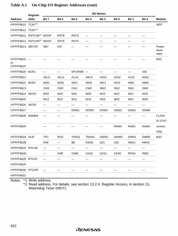
822
Table A.1 On-Chip I/O Register Addresses (cont)
Register Bit Names
Address Abbr. Bit 7 Bit 6 Bit 5 Bit 4 Bit 3 Bit 2 Bit 1 Bit 0 Module
H'FFFF8610 TCNT* 1 WDT
H'FFFF8611 TCNT* 2
H'FFFF8612 RSTCSR* 1 WOVF RSTE RSTS — — — — —
H'FFFF8613 RSTCSR* 2 WOVF RSTE RSTS — — — — —
H'FFFF8614 SBYCR SBY HIZ — — — — — — Power-downstate
H'FFFF8615toH'FFFF861F
— — — — — — — — — BSC
H'FFFF8620 BCR1 — — MTURWE — — — — IOE
H'FFFF8621 A3LG A2LG A1LG A0LG A3SZ A2SZ A1SZ A0SZ
H'FFFF8622 BCR2 IW31 IW30 IW21 IW20 IW11 IW10 IW01 IW00
H'FFFF8623 CW3 CW2 CW1 CW0 SW3 SW2 SW1 SW0
H'FFFF8624 WCR1 W33 W32 W31 W30 W23 W22 W21 W20
H'FFFF8625 W13 W12 W11 W10 W03 W02 W01 W00
H'FFFF8626 WCR2 — — — — — — — —
H'FFFF8627 — — DDW1 DDW0 DSW3 DSW2 DSW1 DSW0
H'FFFF8628 RAMER — — — — — — — — FLASH
(F-ZTAT
H'FFFF8629 — — — — — RAMS RAM1 RAM0 version
only)
H'FFFF862A DCR TPC RCD TRAS1 TRAS0 DWW1 DWW0 DWR1 DWR0 BSC
H'FFFF862B DIW — BE RASD SZ1 SZ0 AMX1 AMX0
H'FFFF862C RTCSR — — — — — — — —
H'FFFF862D — CMF CMIE CKS2 CKS1 CKS0 RFSH RMD
H'FFFF862E RTCNT — — — — — — — —
H'FFFF862F
H'FFFF8630 RTCOR — — — — — — — —
H'FFFF8631
Notes: * 1 Write address.* 2 Read address. For details, see section 13.2.4, Register Access, in section 13,
Watchdog Timer (WDT).

823
Table A.1 On-Chip I/O Register Addresses (cont)
Register Bit Names
Address Abbr. Bit 7 Bit 6 Bit 5 Bit 4 Bit 3 Bit 2 Bit 1 Bit 0 Module
H'FFFF8632toH'FFFF86AF
— — — — — — — — — BSC
H'FFFF86B0 DMAOR — — — — — — PR1 PR0 DMAC
H'FFFF86B1 — — — — — AE NMIF DME
H'FFFF86B2toH'FFFF86BF
— — — — — — — — —
H'FFFF86C0 SAR0
H'FFFF86C1
H'FFFF86C2
H'FFFF86C3
H'FFFF86C4 DAR0
H'FFFF86C5
H'FFFF86C6
H'FFFF86C7
H'FFFF86C8 DMATCR0 — — — — — — — —
H'FFFF86C9
H'FFFF86CA
H'FFFF86CB
H'FFFF86CC CHCR0 — — — — — — — —
H'FFFF86CD — — — DI RO RL AM AL
H'FFFF86CE DM1 DM0 SM1 SM0 RS3 RS2 RS1 RS0
H'FFFF86CF — DS TM TS1 TS0 IE TE DE
H'FFFF86D0 SAR1
H'FFFF86D1
H'FFFF86D2
H'FFFF86D3
H'FFFF86D4 DAR1
H'FFFF86D5
H'FFFF86D6
H'FFFF86D7
H'FFFF86D8 DMATCR1 — — — — — — — —
H'FFFF86D9
H'FFFF86DA
H'FFFF86DB

824
Table A.1 On-Chip I/O Register Addresses (cont)
Register Bit Names
Address Abbr. Bit 7 Bit 6 Bit 5 Bit 4 Bit 3 Bit 2 Bit 1 Bit 0 Module
H'FFFF86DC CHCR1 — — — — — — — — DMAC
H'FFFF86DD — — — DI RO RL AM AL
H'FFFF86DE DM1 DM0 SM1 SM0 RS3 RS2 RS1 RS0
H'FFFF86DF — DS TM TS1 TS0 IE TE DE
H'FFFF86E0 SAR2
H'FFFF86E1
H'FFFF86E2
H'FFFF86E3
H'FFFF86E4 DAR2
H'FFFF86E5
H'FFFF86E6
H'FFFF86E7
H'FFFF86E8 DMATCR2 — — — — — — — —
H'FFFF86E9
H'FFFF86EA
H'FFFF86EB
H'FFFF86EC CHCR2 — — — — — — — —
H'FFFF86ED — — — DI RO RL AM AL
H'FFFF86EE DM1 DM0 SM1 SM0 RS3 RS2 RS1 RS0
H'FFFF86EF — DS TM TS1 TS0 IE TE DE
H'FFFF86F0 SAR3
H'FFFF86F1
H'FFFF86F2
H'FFFF86F3
H'FFFF86F4 DAR3
H'FFFF86F5
H'FFFF86F6
H'FFFF86F7
H'FFFF86F8 DMATCR3 — — — — — — — —
H'FFFF86F9
H'FFFF86FA
H'FFFF86FB
H'FFFF86FC CHCR3 — — — — — — — —
H'FFFF86FD — — — DI RO RL AM AL
H'FFFF86FE DM1 DM0 SM1 SM0 RS3 RS2 RS1 RS0
H'FFFF86FF — DS TM TS1 TS0 IE TE DE

825
Table A.1 On-Chip I/O Register Addresses (cont)
Register Bit Names
Address Abbr. Bit 7 Bit 6 Bit 5 Bit 4 Bit 3 Bit 2 Bit 1 Bit 0 Module
H'FFFF8700 DTEA DTE7 DTE6 DTE5 DTE4 DTE3 DTE2 DTE1 DTE0 DTC
H'FFFF8701 DTEB DTE7 DTE6 DTE5 DTE4 DTE3 DTE2 DTE1 DTE0
H'FFFF8702 DTEC DTE7 DTE6 DTE5 DTE4 DTE3 DTE2 DTE1 DTE0
H'FFFF8703 DTED DTE7 DTE6 DTE5 DTE4 DTE3 DTE2 DTE1 DTE0
H'FFFF8704 DTEE DTE7 DTE6 DTE5 DTE4 DTE3 DTE2 DTE1 DTE0
H'FFFF8705 — — — — — — — — —
H'FFFF8706 DTCSR — — — — — NMIF AE SWDTE
H'FFFF8707 DTVEC7 DTVEC6 DTVEC5 DTVEC4 DTVEC3 DTVEC2 DTVEC1 DTVEC0
H'FFFF8708 DTBR
H'FFFF8709
H'FFFF870AtoH'FFFF873F
— — — — — — — — —
H'FFFF8740 CCR — — — — — — — — CAC
H'FFFF8741 — — — CEDRAM CECS3 CECS2 CECS1 CECS0
H'FFFF8742toH'FFFF87FF
— — — — — — — — —

826
Appendix B Block Diagrams
PAR
Internaldata bus
RES
PFC
Standby
PAW
PAnDRQ
R
C
D
Q PAnMD
Q PAnIOR
SBYCR
RXDm
Q HIZ
SCI
n = 0, 3m = 0, 1PAR: Port A read signalPAW: Port A write signalRES: Reset signal
PAn/RXDm
Figure B.1 PAn/RXDm Block Diagram
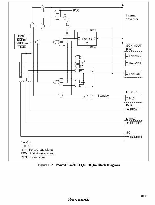
827
PAR
Internaldata bus
RES
SCKmOUTPFC
Standby
PAW
PAnDRQ
C
D
SBYCR
INTCIRQm
n = 2, 5m = 0, 1PAR: Port A read signalPAW: Port A write signalRES: Reset signal
DMACDREQm
SCISCKmIN
Q PAnMD0
Q PAnIOR
Q HIZ
Q PAnMD1
PAn/ SCKm/
DREQm/IRQm
Figure B.2 PAn/SCKm/DREQm/IRQm Block Diagram

828
PAR
Internaldata bus
RES
PFC
CS2, CS3
Standby
PAW
PAnDRQ
C
D
Q PAnMD0
Q PAnMD1
Q PAnIOR
Q HIZ
TCLKA,TCLKB
SBYCR
MTU
n = 6, 7PAR: Port A read signalPAW: Port A write signalRES: Reset signal
RPA6/TCLKA/
CS2,PA7/
TCLKB/CS3
Figure B.3 PA6/TCLKA/CS2, PA7/TCLKB/ CS3 (ZTAT, Mask) Block Diagram
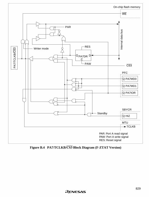
829
Q PA7MD0
Q PA7MD1
PAR
RES
PAW
CDQ PA7DR
PFC
SBYCR
WE
Q HIZ
MTUTCLKB
CS3
Q PA7IOR
PA
7/T
CLK
B/C
S3
PAR: Port A read signalPAW: Port A write signalRES: Reset signal
On-chip flash memory
Writer mode Inte
rnal
dat
a bu
s
Standby
Figure B.4 PA7/TCLKB/CS3 Block Diagram (F-ZTAT Version)

830
PAR
Internaldata bus
RES
PFC
Standby
PAW
PAnDRQ
C
D
TCLKC,TLCKD
SBYCR
MTU
n = 8, 9PAR: Port A read signalPAW: Port A write signalRES: Reset signal
IRQ2,IRQ3
INTC
R
Q PAnMD0
Q PAnMD1
Q PAnIOR
Q HIZ
PA8/TCLKC/IRQ2,PA9/
TCLKD/IRQ3
Figure B.5 PAn/TCLKm/IRQx Block Diagram (ZTAT, Mask)
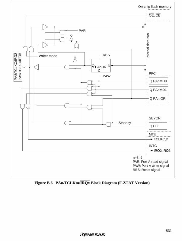
831
Q PAnMD0
Q PAnMD1
PAR
RES
PAW
CDQ PAnDR
PFC
SBYCR
OE, CE
Q HIZ
MTUTCLKC,D
INTCIRQ2,IRQ3
Q PAnIOR
PA
8/T
CLK
C/IR
Q2
PA
9/T
CLK
D/IR
Q3
n=8, 9PAR: Port A read signalPAW: Port A write signalRES: Reset signal
On-chip flash memory
Writer mode Inte
rnal
dat
a bu
s
Standby
Figure B.6 PAn/TCLKm/IRQx Block Diagram (F-ZTAT Version)
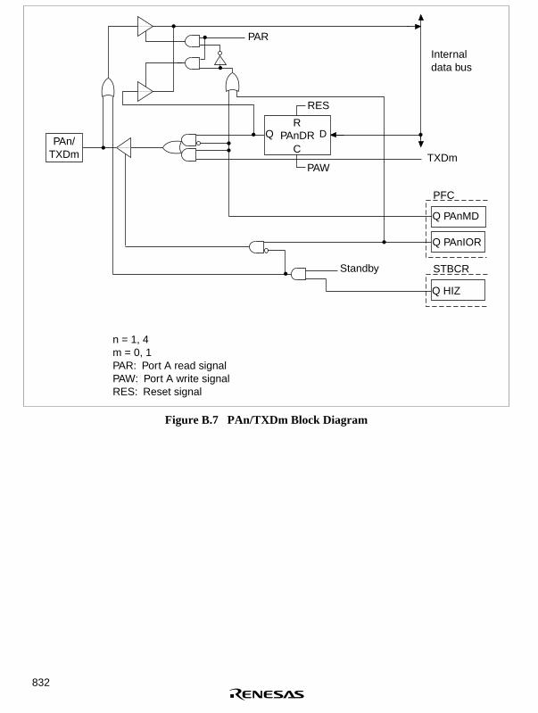
832
PAR
Internaldata bus
RES
TXDm
PFC
Standby
PAW
Q PAnMD
Q PAnIOR
Q HIZ
STBCR
n = 1, 4m = 0, 1PAR: Port A read signalPAW: Port A write signalRES: Reset signal
PAnDRQC
DR
PAn/TXDm
Figure B.7 PAn/TXDm Block Diagram

833
PAR
Internaldata bus
RES
CK
Single mode
MCU mode 2MCU mode 1MCU mode 0
PFC
Standby
PAW
STBCR
PAR: Port A read signalPAW: Port A write signalRES: Reset signal
PA15DRQC
DR
PA15/CK
Q PA15IOR
Q PA15MD
Q HIZ
Figure B.8 PA15/CK Block Diagram

834
PAR
Internaldata bus
RES
DRAK0
PFC
Standby
PAW
SBYCR
PAR: Port A read signalPAW: Port A write signalRES: Reset signal
PA18DRQ
C
DR
BSC
BREQ
PA18/DRAK0/BREQ
Q PA18IMD1
Q PA18IOR
Q PA18MD0
Q HIZ
Figure B.9 PA18/DRAK0/BREQ Block Diagram

835
PAR
Internaldata bus
RES
DRAK1BACK
PFC
Standby
Bus rightrelease
PAW
SBYCR
PAR: Port A read signalPAW: Port A write signalRES: Reset signal
PA19DRQ
C
DR
Q HIZ
PA19/DRAK1/BACK
Q PA19MD0
Q PA19MD1
Q PA19IOR
Figure B.10 PA19/DRAQ1/BACK Block Diagram

836
PAR
Internaldata bus
RES
CS0, CS1,WRL,WRH,RDSingle mode
MCU mode 0MCU mode 1
MCU mode 2
PFC
SBYCRStandby
Bus rightrelease
PAW
n = 10-14PAR: Port A read signalPAW: Port A write signalRES: Reset signal
PAnDRQ
C
DR
Q PAnMD
Q PAnIOR
Q HIZ
PAn/XXX
Figure B.11 PAn/XXX Block Diagram

837
PAR
Internaldata bus
RES
AH, CASHL,CASHH,WRHL,WRHHSingle mode
PFC
SBYCRStandby
Bus rightrelease
PAW
n = 16,20-23PAR: Port A read signalPAW: Port A write signalRES: Reset signal
PAnDRQ
C
DR
Q PAnMD
Q HIZ
Q PAnIOR
PAn/XXXX
Figure B.12 PAn/XXXX Block Diagram

838
PAR
Internaldata bus
RES
Single mode
PFC
SBYCRStandby
Bus rightrelease
PAW
PAR: Port A read signalPAW: Port A write signalRES: Reset signal
PAnDRQ
C
DR
Q PA17MD
Q HIZ
WAITrequest
Q PA17IOR
PA17/WAIT
Figure B.13 PA17/WAIT Block Diagram

839
PBR
PROM mode
Internaldata bus
RES
Single mode
MCU mode 0MCU mode 1
MCU mode 2
A16
PFC
SBYCRStandby
Bus rightrelease
PBW
PBR: Port B read signalPBW: Port B write signalRES: Reset signal
PB0DRQ
C
DR
On-chip*
EPROM
A16
PB0/A16
Q PB0MD
Q PB0IOR
Q HIZ
Note: * Not available with the mask versions.
Figure B.14 PB0/A16 Block Diagram

840
Q PB0MD0
Q PB0IOR
PBR
A16
RES
PBW
CDQ
CPB0DR
PFC
SBYCR
Q HIZ
A16
PBR: Port B read signalPBW: Port B write signalRES: Reset signal
On-chip flash memory
Writer mode Inte
rnal
dat
a bu
s
Single mode
MCU mode 0MCU mode 1
MCU mode 2
Bus right release
Standby
PB
0/A
16
Figure B.15 PB0/A16 Block Diagram (F-ZTAT Version)

841
PBR
Internaldata bus
RES
Single mode
MCU mode 0MCU mode 1
MCU mode 2
A17
PFC
SBYCRStandby
Bus rightrelease
PBW
PBR: Port B read signalPBW: Port B write signalRES: Reset signal
PB1DRQC
D
R
PB1/A17
Q PB1MD
Q PB1IOR
Q HIZ
Figure B.16 PB1/A17 Block Diagram

842
PBR
Internaldata bus
RES
A18BACKPFC
SBYCR
INTCIRQ4
Standby
Bus rightrelease
PBW
PBR: Port B read signalPBW: Port B write signalRES: Reset signal
PB6DRQC
D
Q PB6MD0
Q PB6MD1
Q PB6IOR
Q HIZ
PB6/IRQ4/A18/
BACK
Figure B.17 PB6/IRQ4/A18/BACK Block Diagram

843
PBR
PROM mode
Internaldata bus
RES
CASL, CASHPFC
SBYCR
POE
POEm
Standby
Bus rightrelease
PBW
n = 3, 4m = 1, 2PBR: Port B read signalPBW: Port B write signalRES: Reset signal
PBnDRQ
C
D
On-chip*
EPROM
OE, PGM
Q PBnMD0
Q PBnMD1
Q HIZ
Q PBnIOR
INTC
IRQm
PBn/IRQm/POEm/CASx
Note: * Not available with the ZTAT version.
Figure B.18 PBn/IRQm/POEm/CASx Block Diagram

844
Q PBnMD0
Q PBnMD1
Q PBnIOR
PBR
A17
RES
PBW
CDQ
CPBnDR
PFC
SBYCR
Q HIZ
CASL,CASH
POE
POEm
INTC
IRQm
PB
4/IR
Q2/
PO
E2/
CA
SH
,P
B3/
IRQ
1/P
OE
1/C
AS
L
n=3, 4m=1, 2PBR: Port B read signalPBW: Port B write signalRES: Reset signalNote: * Only when n = 4.
On-chip flash memory*
Inte
rnal
dat
a bu
s
Writer mode
Standby
Bus right release
Figure B.19 PB4/IRQ2/POE2/CASH,PB3/IRQ1/POE1/CASLBlock Diagram (F-ZTAT Version)

845
PBR
Internaldata bus
RES
A19–A21PFC
SBYCR
BSC/AD
BREQ, WAIT,ADTRG
Standby
Bus rightrelease
PBW
n = 7-9m = 5-7PBR: Port B read signalPBW: Port B write signalRES: Reset signal
PBnDRQC
D
Q PBnMD0
Q PBnMD1
Q HIZ
Q PBnIOR
INTC
IRQm
PBn/IRQm/XXX/YYY
Figure B.20 PBn/IRQm/XXX/YYY Block Diagram

846
PBR
Internaldata bus
RES
RAS, RDWRPFC
SBYCR
POE
POE0,POE3
Standby
Bus rightrelease
PBW
n = 2, 5m = 0, 3PBR: Port B read signalPBW: Port B write signalRES: Reset signal
PBnDRQC
D
Q PBnMD0
Q PBnMD1
Q HIZ
Q PBnIOR
INTC
IRQm
PBn/IRQm/XXX/YYY
Figure B.21 PBn/IRQm/XXXX/YYYY Block Diagram

847
PCR
PROM mode
Internaldata bus
RES
Single mode
MCU mode 0MCU mode 1
MCU mode 2
An
PFC
SBYCRStandby
Bus rightrelease
PCW
n = 0–15PCR: Port C read signalPCW: Port C write signalRES: Reset signal
PCnDRQ
C
DR
On-chip*
EPROM
An
Q PBnMD
Q PBnIOR
Q HIZ
PCn/An
Note: * Not available with the mask versions.
Figure B.22 PCn/An Block Diagram

848
Q PCnMD
Q PCnIOR
PCR
An
RES
PCW
CDQ
CPCnDR
PFC
SBYCR
Q HIZ
AnPC
n/A
n
n=0–15PCR: Port C read signalPCW: Port C write signalRES: Reset signal
On-chip flash memory
Writer mode Inte
rnal
dat
a bu
s
Single mode
Bus right release
Standby
MCU mode 2
MCU mode 0MCU mode 1
Figure B.23 PCn/An Block Diagram (F-ZTAT Version)

849
PDR
PROM mode
Internaldata bus
RES
Single mode
MCU mode 0MCU mode 1
MCU mode 2
DnDout
PFC
SBYCR
Din
Standby
Bus right releaseSLEEP
PDW
n = 0–7PDR: Port D read signalPDW: Port D write signalRES: Reset signalDout: Data output timing signalDin: Data bus input timing signal
PDnDRQC
D
R
On-chip*
EPROM
Dn
Q PDnMD
Q PDnIOR
Q HIZ
PDn/Dn
Note: * Not available with the mask version.
Figure B.24 PDn/Dn Block Diagram
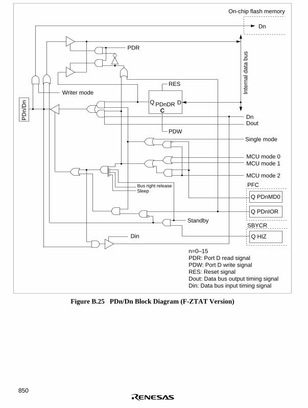
850
Q PDnMD0
Q PDnIOR
Q HIZ
PDR
Dn
RES
PDW
CDQ
CPDnDR
Dout
PFC
SBYCR
Dn
Din
On-chip flash memory
Inte
rnal
dat
a bu
s
PD
n/D
n
Writer mode
Single mode
MCU mode 0MCU mode 1
MCU mode 2
Bus right releaseSleep
Standby
n=0–15PDR: Port D read signalPDW: Port D write signalRES: Reset signalDout: Data bus output timing signalDin: Data bus input timing signal
Figure B.25 PDn/Dn Block Diagram (F-ZTAT Version)

851
Din
Standby
SLEEP
Bus rightrelease
PDn/Dn/IRQm
PDW
RES
RQ D
CPDnDR
PDR
DnDout
Singlemode
MCU mode 1
MCU mode 0
MCU mode 2
PFC
SBYCR
Q HIZ
QPDnMD0
QPDnMD1
QPDnIOR
INTC
IRQm
Internaldata bus
n = 16–23m = 0–7PDR: Port D read signalPDW: Port D write signal
RES: Reset signalDout: Data output timing signalDin: Data bus input timing signal
Figure B.26 PDn/Dn/IRQm Block Diagram (n = 16–23)

852
Din
Standby
SLEEP
Bus rightrelease
PDn/Dn/DREQm
PDW
RES
RQ D
CPDnDR
PDR
DnDout
Singlemode
MCU mode 1
MCU mode 0
MCU mode 2
PFC
SBYCR
Q HIZ
QPDnMD0
QPDnMD1
QPDnIOR
DMAC
DREQm
Internaldata bus
n = 24,25m = 0,1PDR: Port D read signalPDW: Port D write signal
RES: Reset signalDout: Data output timing signalDin: Data bus input timing signal
Figure B.27 PDn/Dn/DREQm Block Diagram (n = 24, 25)

853
Din
Standby
SLEEP
Bus rightrelease
PDn/Dn/DACKm
PDW
RES
RQ D
CPDnDR
PDR
DnDout
Singlemode
MCU mode 1
MCU mode 0
MCU mode 2
PFC
SBYCR
Q HIZ
QPDnMD0
QPDnMD1
QPDnIOR
Internaldata bus
n = 26,27m = 0,1PDR: Port D read signalPDW: Port D write signal
RES: Reset signalDout: Data output timing signalDin: Data bus input timing signal
DACKm
Figure B.28 PDn/Dn/DACKm Block Diagram (n = 26, 27)

854
Din
Standby
SLEEP
Bus rightrelease
PDn/Dn/CSm
PDW
RES
RQ D
CPDnDR
PDR
DnDout
Singlemode
MCU mode 1
MCU mode 0MCU mode 2
PFC
SBYCR
Q HIZ
QPDnMD0
QPDnMD1
QPDnIOR
Internaldata bus
n = 28–29m = 2–3PDR: Port D read signalPDW: Port D write signal
RES: Reset signalDout: Data output timing signalDin: Data bus input timing signal
CSm
Figure B.29 PDn/Dn/CSm Block Diagram (n = 28, 29)
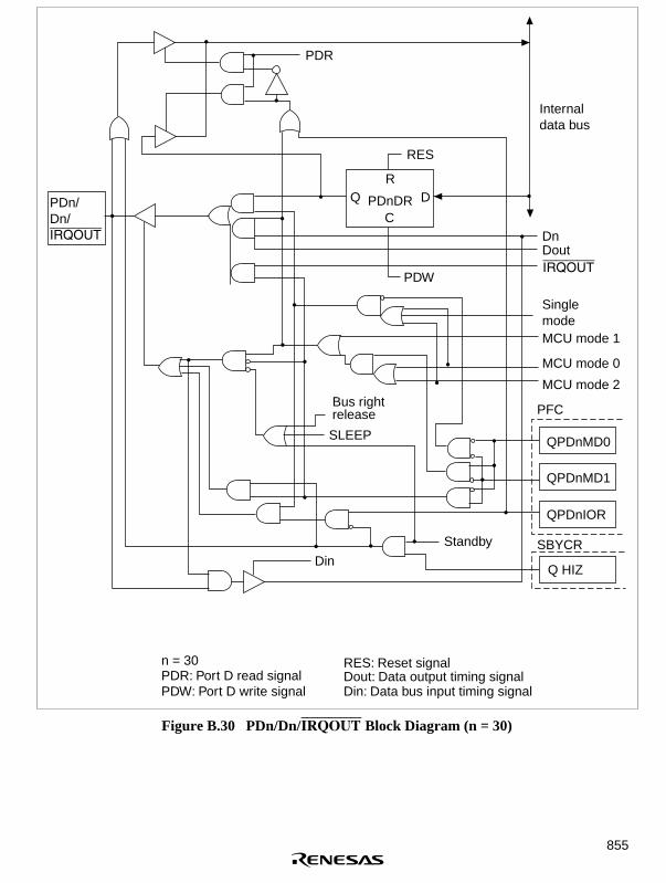
855
Din
Standby
SLEEP
Bus rightrelease
PDn/Dn/IRQOUT
PDW
RES
RQ D
CPDnDR
PDR
DnDout
SinglemodeMCU mode 1
MCU mode 0
MCU mode 2
PFC
SBYCR
Q HIZ
QPDnMD0
QPDnMD1
QPDnIOR
Internaldata bus
n = 30PDR: Port D read signalPDW: Port D write signal
RES: Reset signalDout: Data output timing signalDin: Data bus input timing signal
IRQOUT
Figure B.30 PDn/Dn/IRQOUT Block Diagram (n = 30)
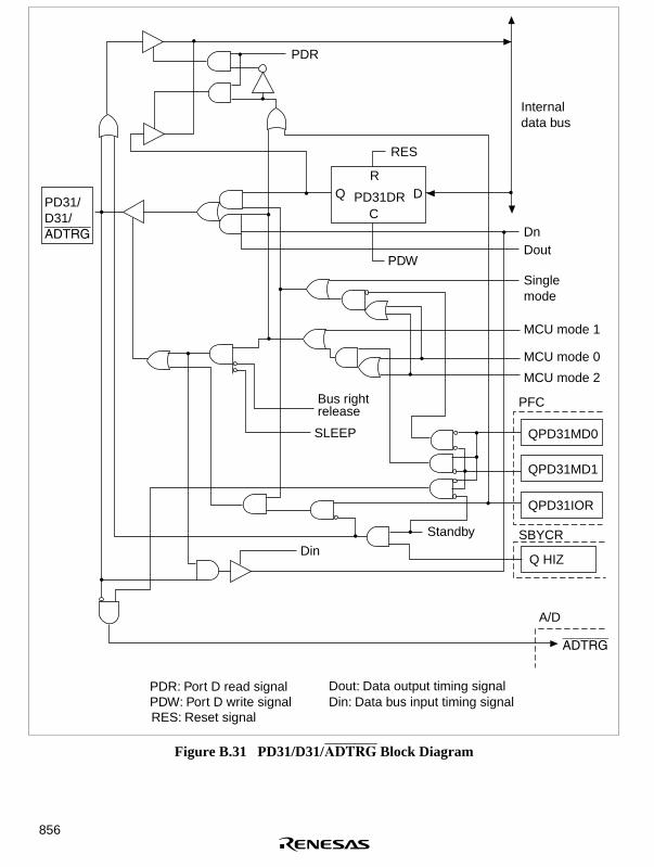
856
Din
Standby
SLEEP
Bus rightrelease
PD31/D31/ADTRG
PDW
RES
RQ D
CPD31DR
PDR
DnDout
Singlemode
MCU mode 1
MCU mode 0
MCU mode 2
PFC
SBYCR
Q HIZ
QPD31MD0
QPD31MD1
QPD31IOR
A/D
ADTRG
Internaldata bus
PDR: Port D read signalPDW: Port D write signalRES: Reset signal
Dout: Data output timing signalDin: Data bus input timing signal
Figure B.31 PD31/D31/ADTRG Block Diagram

857
Din
Standby
SLEEP
Bus right release
PDn/Dn
PDW
RES
RQ D
CPDnDR
PDR
DnDout
Singlemode
MCU mode 1MCU mode 0
MCU mode 2
PFC
Q HIZ
QPDnMD
QPDnIOR
Internaldata bus
n = 8–15PDR: Port D read signalPDW: Port D write signal
RES: Reset signalDout: Data output timing signalDin: Data bus input timing signal
SBYCR
Figure B.32 PDn/Dn Block Diagram

858
Standby
PE13/TIOC4B/MRES PEW
RES
Q D
CPE13DR
PER
PFC
SBYCR
Q HIZ
QPE13MD0
QPE13MD1
QPE13IOR
SYSC
MRES
Internaldata bus
PER: Port E read signalPEW: Port E write signalRES: Reset signal
MTU
TIOC4B
TIOC4B
Figure B.33 PE13/TIOC4B/MRES Block Diagram

859
Standby
PE14/TIOC4C/DACK0/AH
PEW
RES
Q D
CPE14DR
PER
PFC
SBYCR
Q HIZ
QPE14MD0
QPE14MD1
QPE14IOR
Internaldata bus
PER: Port E read signalPEW: Port E write signalRES: Reset signal
MTU
TIOC4C
TIOC4CDRAK0
AH
Figure B.34 PE14/TIOC4C/DACK0/AH Block Diagram

860
Standby
PE15/TIOC4D/DACK1/IRQOUT PEW
RES
Q D
CPE15DR
PER
PFC
SBYCR
Q HIZ
QPE15MD0
QPE15MD1
QPE15IOR
Internaldata bus
PER: Port E read signalPEW: Port E write signalRES: Reset signal
MTU
TIOC4D
TIOC4DDRAK1
IRQOUT
Figure B.35 PEn/TIOC4D/DACK1/IRQOUT Block Diagram
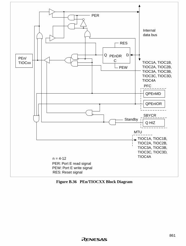
861
Standby
PEn/TIOCxx
PEW
RES
Q D
CPEnDR
PER
PFC
SBYCR
Q HIZ
QPEnMD
QPEnIOR
Internaldata bus
PER: Port E read signalPEW: Port E write signalRES: Reset signal
MTU
TIOC1A, TIOC1B,TIOC2A, TIOC2B,TIOC3A, TIOC3B,TIOC3C, TIOC3D,TIOC4A
n = 4-12
TIOC1A, TIOC1B,TIOC2A, TIOC2B,TIOC3A, TIOC3B,TIOC3C, TIOC3D,TIOC4A
Figure B.36 PEn/TIOCXX Block Diagram

862
Standby
PEn/TIOCxx/DRACm
PEW
RES
Q D
CPEnDR
PER
PFC
SBYCR
Q HIZ
QPEnMD0
QPEnMD1
QPEnIOR
Internaldata bus
PER: Port E read signalPEW: Port E write signalRES: Reset signal
MTU
TIOC0BTIOC0D
TIOC0BTIOC0DDRAKm
n = 1, 3m = 0, 1
Figure B.37 PEn/TIOCXX/DRAKm Block Diagram

863
Standby
PEn/TIOCxx/DREQm PEW
RES
Q D
CPEnDR
PER
PFC
SBYCR
Q HIZ
QPEnMD0
QPEnMD1
QPEnIOR
DMA
DREQm
Internaldata bus
PER: Port E read signalPEW: Port E write signalRES: Reset signal
MTU
TIOC0ATIOC0C
TIOC0ATIOC0C
n = 0, 2m = 0, 1
Figure B.38 PEn/TIOCXX/DREQm Block Diagram

864
Internaldata bus
StandbySBYCR
Q HIZ
AD
ANn
PFR
PFn/ANn
n = 0–7PFR: Port F read signal
Figure B.39 PFn/ANn Block Diagram

865
Appendix C Pin States
Table C.1 Pin Modes During Reset, Power-Down, and Bus Right Release Modes (144 Pin)
Pin modes
Pin Function Reset Power-Down Bus Right Standby in BusClass Pin Name Power-OnManual Standby Sleep Release Right Release
Clock CK O O H* 1 O O O
System RES I I I I I Icontrol MRES Z* 4 I Z I I Z
WDTOVF O* 3 O* 3 O O O O
BREQ Z* 4 I Z I I I
BACK Z* 4 O Z O L L
Interrupt NMI I I I I I I
IRQ0–IRQ7 Z* 4 I Z I I Z
IRQOUT (PD30) Z* 4 O H* 1 H O H* 1
IRQOUT (PE15) Z* 4 O Z H O Z
Addressbus
A0–A21 O* 2 O Z O Z Z
Data bus D0–D31 Z* 4 I/O Z I/O Z Z
Bus WAIT Z* 4 I Z I Z Zcontrol RD/WR, RAS Z* 4 O O O Z Z
CASH, CASL,CASLH, CASLL
Z* 4 O O O Z Z
RD H O Z O Z Z
CS0, CS1 H O Z O Z Z
CS2, CS3 Z* 4 O Z O Z Z
WRHH, WRHL,WRH, WRL
H O Z O Z Z
AH Z* 4 O Z O Z Z
DMAC DACK0, DACK1(PD26, PD27)
Z* 4 O O* 1 O O O* 1
DACK0, DACK1(PE14, PE15)
Z* 4 O Z O O Z
DRAK0, DRAK1 Z* 4 O O* 1 O O O* 1
DREQ0, DREQ1 Z* 4 I Z I I Z

866
Table C.1 Pin Modes During Reset, Power-Down, and Bus Right Release Modes (144 Pin)(cont)
Pin modes
Pin Function Reset Power-Down Bus Right Standby in BusClass Pin Name Power-OnManual Standby Sleep Release Right Release
MTU TIOC0A–TIOC0D,TIOC1A–TIOC1D,TIOC2A–TIOC2D,TIOC3A, TIOC3C
Z* 4 I/O K* 1 I/O I/O K* 1
TIOC3B,TIOC3D,TIOC4A–TIOC4D
Z* 4 I/O Z I/O I/O Z
TCLKA–TCLKD Z* 4 I Z I I Z
Portcontrol
POE0–POE3 Z* 4 I Z I I Z
SCI SCK0–SCK1 Z* 4 I/O Z I/O I/O Z
TXD0–TCD1 Z* 4 O O* 1 O O O* 1
RXD0–RXD1 Z* 4 I Z I I Z
A/D ADTRG Z* 4 I Z I I Zconverter AN0–AN7 Z I Z I I Z
I/O Port PA0–PA23 Z* 4 I/O K* 1 K I/O K* 1
PB0–PB9
PC0–PC15
PD0–PD31
PE0–PE8,PE10
PE9,PE11–PE15 Z* 4 I/O Z K I/O Z
PF0–PF17 Z I Z I I Z
Notes: 1. There are instances where bus right release and transition to software standby modeoccur simultaneously due to the timing between BREQ and internal operations. In suchcases, standby mode results, but the standby state may be different.The initial pin states depend on the mode. See section 18, Pin Function Controller, fordetails.
2. I: Input, O: Output, H: High-level output, L: Low-level output, Z: High impedance,K: Input pin with high impedance, output pin mode maintained.
* 1 If the standby control register port high-impedance bits are set to 1, output pins becomehigh impedance.
* 2 A21–A18 will become input ports after power-on reset.* 3 Input in the SH7044/SH7045 F-ZTAT version.* 4 General use I/O ports PAn, PBn, PCn, PDn, and PEn, as well as pins multiplexed with
them, are unstable during the RES setup time (tRESS) immediately after the RES pingoes to low level.

867
Table C.2 Pin Modes During Reset, Power-Down, and Bus Right Release Modes (112 Pin,120 Pin)
Pin modes
Pin Function Reset Power-Down Bus Right Standby in BusClass Pin Name Power-On Manual Standby Sleep Release Right Release
Clock CK O O H* 1 O O O
System RES I I I I I Icontrol MRES Z* 4 I Z I I Z
WDTOVF O* 3 O* 3 O O O O
BREQ Z* 4 I Z I I I
BACK Z* 4 O Z O L L
Interrupt NMI I I I I I I
IRQ0–IRQ7 Z* 4 I Z I I Z
IRQOUT Z* 4 O Z H O Z
Addressbus
A0–A21 O* 2 O Z O Z Z
Data bus D0–D31 Z* 4 I/O Z I/O Z Z
Bus WAIT Z* 4 I Z I Z Zcontrol RDWR, RAS Z* 4 O O O Z Z
CASH, CASL Z* 4 O O O Z Z
RD H O Z O Z Z
CS0, CS1 H O Z O Z Z
CS2, CS3 Z* 4 O Z O Z Z
WRH, WRL H O Z O Z Z
AH Z* 4 O Z O Z Z
DMAC DACK0–DACK1 Z* 4 O Z O O Z
DRAK0–DRAK1 Z* 4 O Z O O Z
DREQ0–DREQ1 Z* 4 I Z I I Z
MTU TIOC0A–TIOC0D,TIOC1A–TIOC1D,TIOC2A–TIOC2D,TIOC3A, TIOC3C
Z* 4 I/O K* 1 I/O I/O K* 1
TIOC3B,TIOC3D,TIOC4A–TIOC4D
Z* 4 I/O Z I/O I/O Z
TCLKA–TCLKD Z* 4 I Z I I Z

868
Table C.2 Pin Modes During Reset, Power-Down, and Bus Right Release Modes (112 Pin,120 Pin) (cont)
Pin modes
Pin Function Reset Power-Down Bus Right Standby in BusClass Pin Name Power-On Manual Standby Sleep Release Right Release
Portcontrol
POE0–POE3 Z* 4 I Z I I Z
SCI SCK0–SCK1 Z* 4 I/O Z I/O I/O Z
TXD0–TCD1 Z* 4 O O* 1 O O O* 1
RXD0–RXD1 Z* 4 I Z I I Z
A/Dconverter
ADTRG Z* 4 I Z I I Z
control AN0–AN7 Z I Z I I Z
I/O Port PA0–PA15 Z* 4 I/O K* 1 K I/O K* 1
PB0–PB9
PC0–PC15
PD0–PD15
PE0–PE8–PE10
PE9,PE11–PE15 Z* 4 I/O Z K I/O Z
PF0–PF7 Z I Z I I Z
Notes: 1. There are instances where bus right release and transition to software standby modeoccur simultaneously due to the timing between BREQ and internal operations. In suchcases, standby mode results, but the standby state may be different.The initial pin states depend on the mode. See section 18, Pin Function Controller, fordetails.
2. I: Input, O: Output, H: High-level output, L: Low-level output, Z: High impedance,K: Input pin with high impedance, output pin mode maintained.
* 1 If the standby control register port high-impedance bits are set to 1, output pins becomehigh impedance.
* 2 A21–A18 will become input ports after power-on reset.* 3 Input in the SH7044/SH7045 F-ZTAT version.* 4 General use I/O ports PAn, PBn, PCn, PDn, and PEn, as well as pins multiplexed with
them, are unstable during the RES setup time (tRESS) immediately after the RES pingoes to low level.
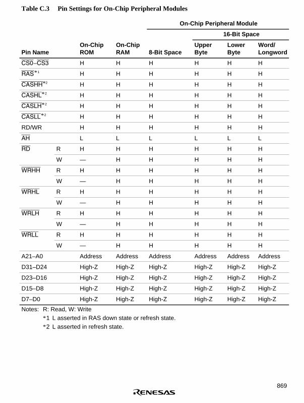
869
Table C.3 Pin Settings for On-Chip Peripheral Modules
On-Chip Peripheral Module
16-Bit Space
Pin NameOn-ChipROM
On-ChipRAM 8-Bit Space
UpperByte
LowerByte
Word/Longword
CS0–CS3 H H H H H H
RAS* 1 H H H H H H
CASHH* 2 H H H H H H
CASHL* 2 H H H H H H
CASLH* 2 H H H H H H
CASLL* 2 H H H H H H
RD/WR H H H H H H
AH L L L L L L
RD R H H H H H H
W — H H H H H
WRHH R H H H H H H
W — H H H H H
WRHL R H H H H H H
W — H H H H H
WRLH R H H H H H H
W — H H H H H
WRLL R H H H H H H
W — H H H H H
A21–A0 Address Address Address Address Address Address
D31–D24 High-Z High-Z High-Z High-Z High-Z High-Z
D23–D16 High-Z High-Z High-Z High-Z High-Z High-Z
D15–D8 High-Z High-Z High-Z High-Z High-Z High-Z
D7–D0 High-Z High-Z High-Z High-Z High-Z High-Z
Notes: R: Read, W: Write* 1 L asserted in RAS down state or refresh state.* 2 L asserted in refresh state.

870
Table C.4 Pin Settings for Normal External Space
16-Bit Space
Pin Name 8-Bit Space Upper Word Lower Word Word/Longword
CS0–CS3 Valid Valid Valid Valid
RAS* 1 H H H H
CASHH* 2 H H H H
CASHL* 2 H H H H
CASLH* 2 H H H H
CASLL* 2 H H H H
RD/WR H H H H
AH L L L L
RD R L L L L
W H H H H
WRHH R H H H H
W H H H H
WRHL R H H H H
W H H H H
WRLH R H H H H
W H L H L
WRLL R H H H H
W L H L L
A21–A0 Address Address Address Address
D31–D24 High-Z High-Z High-Z High-Z
D23–D16 High-Z High-Z High-Z High-Z
D15–D8 High-Z Data High-Z Data
D7–D0 Data High-Z Data Data

871
Table C.4 Pin Settings for Normal External Space (cont)
32-Bit Space
Pin Name MSB 2nd Byte 3rd Byte LSBUpperWord
LowerWord Longword
CS0–CS3 Valid Valid Valid Valid Valid Valid Valid
RAS* 1 H H H H H H H
CASHH* 2 H H H H H H H
CASHL* 2 H H H H H H H
CASLH* 2 H H H H H H H
CASLL* 2 H H H H H H H
RD/WR H H H H H H H
AH L L L L L L L
RD R L L L L L L L
W H H H H H H H
WRHH R H H H H H H H
W L H H H L H L
WRHL R H H H H H H H
W H L H H L H L
WRH R H H H H H H H
W H H L H H L L
WRL R H H H H H H H
W H H H L H L L
A21–A0 Address Address Address Address Address Address Address
D31–D24 Data High-Z High-Z High-Z Data High-Z Data
D23–D16 High-Z Data High-Z High-Z Data High-Z Data
D15–D8 High-Z High-Z Data High-Z High-Z Data Data
D7–D0 High-Z High-Z High-Z Data High-Z Data Data
Notes: 1. R: Read, W: Write2. Valid: Chip select signal corresponding with accessed area is low; chip select signal in
other cases is high.* 1 L asserted in RAS down mode or refresh mode.* 2 L asserted in refresh mode.

872
Table C.5 Pin Settings for Multiplex I/O Space
16-Bit Space
Pin Name 8-Bit Space Upper Byte Lower Byte Word/Longword
CS0–CS2 H H H H
CS3 L L L L
RAS* 1 H H H H
CASHH* 2 H H H H
CASHL* 2 H H H H
CASLH* 2 H H H H
CASLL* 2 H H H H
RD/WR H H H H
AH Valid Valid Valid Valid
RD R L L L L
W H H H H
WRHH R H H H H
W H H H H
WRHL R H H H H
W H H H H
WRH R H H H H
W H L H L
WRL R H H H H
W L H L L
A21–A0 Address Address Address Address
D31–D24 High-Z High-Z High-Z High-Z
D23–D16 High-Z High-Z High-Z High-Z
D15–D8 High-Z Address/Data Address Address/Data
D7–D0 Address/Data Address Address/Data Address/Data
Notes: 1. R: Read, W: Write2. Valid: High output in accordance with AH timing.* 1 L asserted in RAS down mode or refresh mode.* 2 L asserted in refresh mode.

873
Table C.6 Pin Settings for DRAM Space
16-Bit Space
Pin Name 8-Bit Space Upper Word Lower Word Word/Longword
CS0–CS3 H H H H
RAS* 1 Valid Valid Valid Valid
CASHH* 2 H H H H
CASHL* 2 H H H H
CASLH* 2 H Valid H Valid
CASLL* 2 Valid H Valid Valid
RD/WR R H H H H
W L L L L
AH L L L L
RD R L L L L
W H H H H
WRHH R H H H H
W H H H H
WRHL R H H H H
W H H H H
WRH R H H H H
W H L H L
WRL R H H H H
W L H L L
A21–A0 Address Address Address Address
D31–D24 High-Z High-Z High-Z High-Z
D23–D16 High-Z High-Z High-Z High-Z
D15–D8 High-Z Data High-Z Data
D7–D0 Data High-Z Data Data

874
Table C.6 Pin Settings for DRAM Space (cont)
32-Bit Space
Pin Name MSB 2nd Byte 3rd Byte LSBUpperWord
LowerWord Longword
CS0–CS3 H H H H H H H
RAS* 1 Valid Valid Valid Valid Valid Valid Valid
CASHH* 2 Valid H H H Valid H Valid
CASHL* 2 H Valid H H Valid H Valid
CASLH* 2 H H Valid H H Valid Valid
CASLL* 2 H H H Valid H Valid Valid
RD/WR R H H H H H H H
W L L L L L L L
AH L L L L L L L
RD R L L L L L L L
W H H H H H H H
WRHH R H H H H H H H
W L H H H L H L
WRHL R H H H H H H H
W H L H H L H L
WRH R H H H H H H H
W H H L H H L L
WRL R H H H H H H H
W H H H L H L L
A21–A0 Address Address Address Address Address Address Address
D31–D24 Data High-Z High-Z High-Z Data High-Z Data
D23–D16 High-Z Data High-Z High-Z Data High-Z Data
D15–D8 High-Z High-Z Data High-Z High-Z Data Data
D7–D0 High-Z High-Z High-Z Data High-Z Data Data
Notes: 1. R: Read, W: Write2. Valid: Chip select signal corresponding with accessed area is low; chip select signal in
other cases is high.* 1 Asserted in RAS down mode or refresh mode.* 2 Asserted in refresh mode.

875
Appendix D Notes when Converting the F–ZTATApplication Software to the Mask-ROM Versions
Please note the following when converting the F-ZTAT application software to the mask-ROMversions.
The values read from the internal registers for the flash ROM of the mask-ROM version and F–ZTAT version differ as follows.
Status
Register Bit F–ZTAT Version Mask-ROM Version
FLMCR1 FWE 0: Application softwarerunning
1: Programming
0: Is not read out
1: Application softwarerunning
Note: This difference applies to all the F-ZTAT versions and all the mask-ROM versions that havedifferent ROM size.

876
Appendix E Product Code Lineup
Table E.1 SH7040, SH7041, SH7042, SH7043, SH7044, and SH7045 Product Lineup
Product
Type
Mask
Version Product Code Mark Code Package Order Model No. * 2
SH7040A Mask ROM A MASK HD6437040AF28 HD6437040A (*** )F28 QFP2020-112 HD6437040A*** F
verion HD6437040AVF16 HD6437040A(*** )VF16 QFP2020-112 HD6437040A*** F
HD6437040AVX16 HD6437040A(*** )VX16 TQFP1414-120 HD6437040A*** X
HD6437040ACF28 HD6437040A(*** )CF28 QFP2020-112Cu* 1 HD6437040A*** CF
HD6437040AVCF16 HD6437040A(*** )VCF16 QFP2020-112Cu* 1 HD6437040A*** CF
ROM less A MASK HD6417040AF28 HD6417040AF28 QFP2020-112 HD6417040AF28
version HD6417040AVF16 HD6417040AVF16 QFP2020-112 HD6417040AVF16
HD6417040AVX16 HD6417040AVX16 TQFP1414-120 HD6417040AVX16
HD6417040ACF28 HD6417040ACF28 QFP2020-112Cu* 1 HD6417040ACF28
HD6417040AVCF16 HD6417040AVCF16 QFP2020-112Cu* 1 HD6417040AVCF16
SH7041A Mask ROM A MASK HD6437041AF28 HD6437041A(*** )F28 QFP2020-144 HD6437041A*** F
version HD6437041AVF16 HD6437041A(*** )VF16 QFP2020-144 HD6437041A*** F
HD6437041ACF28 HD6437041A(*** )CF28 QFP2020-144Cu* 1 HD6437041A*** CF
HD6437041AVCF16 HD6437041A(***) VCF16 QFP2020-144Cu* 1 HD6437041A*** CF
ROM less A MASK HD6417041AF28 HD6417041AF28 QFP2020-144 HD6417041AF28
verion HD6417041AVF16 HD6417041AVF16 QFP2020-144 HD6417041AVF16
HD6417041ACF28 HD6417041ACF28 QFP2020-144Cu* 1 HD6417041ACF28
HD6417041AVCF16 HD6417041AVCF16 QFP2020-144Cu* 1 HD6417041AVCF16
SH7042 Mask ROM – HD6437042F28 HD6437042 (*** )F28 QFP2020-112 HD6437042*** F
version HD6437042VF16 HD6437042 (*** )VF16 QFP2020-112 HD6437042*** F
Z-TAT – HD6477042F28 HD6477042F28 QFP2020-112 HD6477042F28
version HD6477042VF16 HD6477042VF16 QFP2020-112 HD6477042VF16
SH7042A Mask ROM A MASK HD6437042AF28 HD6437042A(*** )F28 QFP2020-112 HD6437042A*** F
version HD6437042AVF16 HD6437042A(*** )VF16 QFP2020-112 HD6437042A*** F
HD6437042AVX16 HD6437042A(*** )VX16 TQFP1414-120 HD6437042A*** X
HD6437042ACF28 HD6437042A(*** )CF28 QFP2020-112Cu* 1 HD6437042A*** CF
HD6437042AVCF16 HD6437042A(*** )VCF16 QFP2020-112Cu* 1 HD6437042A*** CF

877
Table E.1 SH7040, SH7041, SH7042, SH7043, SH7044, and SH7045 Product Lineup (cont)
Product
Type
Mask
Version Product Code Mark Code Package Order Model No. * 2
SH7042A Z-TAT A MASK HD6477042AF28 HD6477042AF28 QFP2020-112 HD6477042AF28
version HD6477042AVF16 HD6477042AVF16 QFP2020-112 HD6477042AVF16
HD6477042AVX16 HD6477042AVX16 TQFP1414-120 HD6477042AVX16
HD6477042ACF28 HD6477042ACF28 QFP2020-112Cu* 1 HD6477042ACF28
HD6477042AVCF16 HD6477042AVCF16 QFP2020-112Cu* 1 HD6477042AVCF16
SH7043 Mask ROM – HD6437043F28 HD6437043(*** )F28 QFP2020-144 HD6437043*** F
version HD6437043VF16 HD6437043(*** )VF16 QFP2020-144 HD6437043*** F
Z-TAT – HD6477043F28 HD6477043F28 QFP2020-144 HD6477043F28
version HD6477043VF16 HD6477043VF16 QFP2020-144 HD6477043VF16
SH7043A Mask ROM A MASK HD6437043AF28 HD6437043A(*** )F28 QFP2020-144 HD6437043A*** F
version HD6437043AVF16 HD6437043A(*** )VF16 QFP2020-144 HD6437043A*** F
HD6437043ACF28 HD6437043A(***) CF28 QFP2020-144Cu* 1 HD6437043A*** CF
HD6437043AVCF16 HD6437043A(*** )VCF16 QFP2020-144Cu* 1 HD6437043A*** CF
Z-TAT A MASK HD6477043AF28 HD6477043AF28 QFP2020-144 HD6477043AF28
version HD6477043AVF16 HD6477043AVF16 QFP2020-144 HD6477043AVF16
HD6477043ACF28 HD6477043ACF28 QFP2020-144Cu* 1 HD6477043ACF28
HD6477043AVCF16 HD6477043AVCF16 QFP2020-144Cu* 1 HD6477043AVCF16
SH7044 Mask ROM
version
A MASK HD6437044F28 HD6437044(*** )F28 QFP2020-112 HD6437044*** F
F-ZTAT
version
HD64F7044F28 HD64F7044F28 QFP2020-112 HD64F7044F28
SH7045 Mask ROM
version
A MASK HD6437045F28 HD6437045(*** )F28 QFP2020-144 HD6437045*** F
F-ZTAT
version
HD64F7045F28 HD64F7045F28 QFP2020-144 HD64F7045F28
(*** ) is the ROM code.Notes: * 1 Package with Copper used as the lead material.
* 2 *** in the Order Model No. is the ROM code, consisting of a letter and a two-digitnumber (ex. E00). The letter indicates the voltage and frequency, as shown below.• E, F, G, H: 5.0 V, 28 MHz• P, Q, R: 3.3 V, 16 MHz

878
Appendix F Package Dimensions
Package dimensions of the SH7040, SH7042, SH7044 (FP-112) are shown in figures F.1 and F.2.Package dimensions of the SH7040, SH7042 (TFP-120) are shown in figure F.3.Package dimensions of the SH7041, SH7043, SH7045 (FP-144) are shown in figures F.4 and F.5.
Package CodeJEDECJEITAMass (reference value)
FP-112—Conforms2.4 g
*Dimension including the plating thicknessBase material dimension
0.10
23.2 ± 0.3
*0.32 ± 0.08
0.65
1.6
0.8 ± 0.3
*0.1
7 ±
0.05
3.05
Max
23.2
± 0
.3
84 57
56
29112
1 28
20
85
2.70
0˚ – 8˚
0.13 M
0.10
+0.
15–0
.10
1.23
0.30 ± 0.06
0.15
± 0
.04
Unit: mm
Figure F.1 Package Dimensions (FP-112)

879
This package (FP-112B) uses copper leads.
0.10
23.2 ± 0.2
0.32 ± 0.08
0.65
1.6
0.8 ± 0.2
0.17
± 0
.05
3.05
Max
23.2
± 0
.2
84 57
56
29112
1 28
20
85
2.70
0˚ – 8˚
0.13 M
0.10
+0.
15–0
.10
1.23
0.30 ± 0.06
0.15
± 0
.04
*
*
Package CodeJEDECJEITAMass (reference value)
FP-112B—Conforms2.4 g
*Dimension including the plating thicknessBase material dimension
Unit: mm
Figure F.2 Package Dimensions (FP-112B)

880
Package CodeJEDECJEITAMass (reference value)
TFP-120—Conforms0.5 g
*Dimension including the plating thicknessBase material dimension
16.0 ± 0.2
14
0.07
0.100.5 ± 0.1
16.0
± 0
.2
0.4
0.10
± 0
.10
1.20
Max
*0.1
7 ±
0.05
0˚ – 8˚
90 61
1 30
91
120 31
60
M*0.17 ± 0.05
1.0
1.001.2
0.15 ± 0.04
0.15
± 0
.04
Unit: mm
Figure F.3 Package Dimensions (TFP-120)
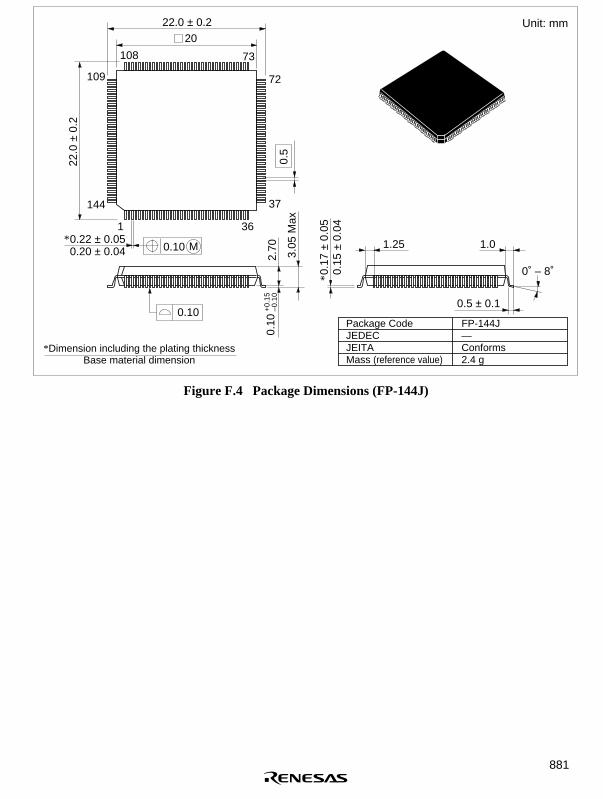
881
Package CodeJEDECJEITAMass (reference value)
FP-144J—Conforms2.4 g
*Dimension including the plating thicknessBase material dimension
0.10 M
20
22.0
± 0
.273
36
144
0.5
0.10
3.05
Max
0˚ – 8˚
22.0 ± 0.2
108
72
37
109
1
0.17
± 0
.05
2.70
0.22 ± 0.05
0.5 ± 0.1
1.0
0.10
+0.
15–0
.10
1.250.20 ± 0.04
0.15
± 0
.04
*
*
Unit: mm
Figure F.4 Package Dimensions (FP-144J)

882
This package (FP-144G) uses copper leads.
Package CodeJEDECJEITAMass (reference value)
FP-144G—Conforms2.4 g
*Dimension including the plating thicknessBase material dimension
0.10 M
2022
.0 ±
0.2
73
36
144
0.5
0.10
3.05
Max
0˚ – 8˚
22.0 ± 0.2
108
72
37
109
1
0.17
± 0
.05
2.70
0.22 ± 0.05
0.5 ± 0.1
1.0
0.10
+0.
15–0
.10
1.250.20 ± 0.04
0.15
± 0
.04
*
*
Unit: mm
Figure F.5 Package Dimensions (FP-144G)

SH7040, SH7041, SH7042, SH7043, SH7044, SH7055 GroupHardware Manual
Publication Date: 1st Edition, February, 1997Rev.6.00, May 26, 2003
Published by: Sales Strategic Planning Div.Renesas Technology Corp.
Edited by: Technical Documentation & Information DepartmentRenesas Kodaira Semiconductor Co., Ltd.
1997, 2003 Renesas Technology Corp. All rights reserved. Printed in Japan.

Colophon 0.0
http://www.renesas.com
Sales Strategic Planning Div. Nippon Bldg., 2-6-2, Ohte-machi, Chiyoda-ku, Tokyo 100-0004, Japan

SH7040, SH7041, SH7042, SH7043,SH7044, SH7055 Group
Hardware Manual
REJ090044-0600O