32-bit RISC Microcontroller - Fujitsu · PDF file32-bit RISC Microcontroller CMOS ... 32 bits...
96
DS07-16305-3E FUJITSU SEMICONDUCTOR DATA SHEET 32-bit RISC Microcontroller CMOS FR30 Series MB91107/108 ■ DESCRIPTION The MB91107 is a standard single-chip microcontroller constructed around the 32-bit RISC CPU (FR* family) core with abundant I/O resources and bus control functions optimized for high-performance/high-speed CPU processing for embedded controller applications. To support the vast memory space accessed by the 32-bit CPU, the MB91107 normally operates in the external bus access mode and executes instructions on the internal 1 Kbyte cache memory and RAM (MB91107: 128 Kbytes, MB91108: 160 Kbytes) for enhanced performance. The MB91107 is optimized for applications requiring high-performance CPU processing such as navigation sys- tems, high-performance FAXs and printer controllers. *: FR Family stands for FUJITSU RISC controller. ■ FEATURES FR CPU • 32-bit RISC, load/store architecture, 5-stage pipeline • Operating clock frequency: Internal 50 MHz/external 25 MHz (PLL used at source oscillation 12.5 MHz) • General purpose registers: 32 bits × 16 • 16-bit fixed length instructions (basic instructions), 1 instruction/1 cycle • Memory to memory transfer, bit processing, barrel shifter processing: Optimized for embedded applications (Continued) ■ PACKAGE 120-pin Plastic LQFP (FPT-120P-M21)
Transcript of 32-bit RISC Microcontroller - Fujitsu · PDF file32-bit RISC Microcontroller CMOS ... 32 bits...
DS07-16305-3EFUJITSU SEMICONDUCTORDATA SHEET
32-bit RISC MicrocontrollerCMOS
FR30 Series
MB91107/108
DESCRIPTIONThe MB91107 is a standard single-chip microcontroller constructed around the 32-bit RISC CPU (FR* family)core with abundant I/O resources and bus control functions optimized for high-performance/high-speed CPUprocessing for embedded controller applications. To support the vast memory space accessed by the 32-bit CPU,the MB91107 normally operates in the external bus access mode and executes instructions on the internal1 Kbyte cache memory and RAM (MB91107: 128 Kbytes, MB91108: 160 Kbytes) for enhanced performance.
The MB91107 is optimized for applications requiring high-performance CPU processing such as navigation sys-tems, high-performance FAXs and printer controllers.
*: FR Family stands for FUJITSU RISC controller.
FEATURESFR CPU
• 32-bit RISC, load/store architecture, 5-stage pipeline• Operating clock frequency: Internal 50 MHz/external 25 MHz (PLL used at source oscillation 12.5 MHz)• General purpose registers: 32 bits × 16• 16-bit fixed length instructions (basic instructions), 1 instruction/1 cycle• Memory to memory transfer, bit processing, barrel shifter processing: Optimized for embedded applications
(Continued) PACKAGE
120-pin Plastic LQFP
(FPT-120P-M21)
MB91107/108
2
• Function entrance/exit instructions, multiple load/store instructions of register contents, instruction systemssupporting high level languages
• Register interlock functions, efficient assembly language coding• Branch instructions with delay slots: Reduced overhead time in branch executions• Internal multiplier/supported at instruction level
Signed 32-bit multiplication: 5 cyclesSigned 16-bit multiplication: 3 cycles
• Interrupt (push PC and PS): 6 cycles, 16 priority levels
Bus interface
• Clock doubler: Internal 50 MHz, external bus 25 MHz operation• 25-bit address bus (32 Mbytes memory space)• 8/16-bit data bus• Basic external bus cycle: 2 clock cycles• Chip select outputs for setting down to a minimum memory block size of 64 Kbytes: 8• Interface supported for various memory technologies
DRAM interface (area 4 and 5)• Automatic wait cycle insertion: Flexible setting, from 0 to 7 for each area• Unused data/address pins can be configured us input/output ports• Little endian mode supported (Select 1 area from area 1 to 5)
DRAM interface
• 2 banks independent control (area 4 and 5)• Double CAS DRAM (normal DRAM I/F) / Single CAS DRAM / Hyper DRAM• Basic bus cycle: Normally 5 cycles, 2-cycle access possible in high-speed page mode• Programmable waveform: Automatic 1-cycle wait insertion to RAS and CAS cycles• DRAM refresh
CBR refresh (interval time configurable by 6-bit timer)Self-refresh mode
• Supports 8/9/10/12-bit column address width• 2CAS/1WE, 2WE/1CAS selective
Cache memory
• 1-Kbyte instruction cache memory• 2 way set associative• 32 block/way, 4 entry(4 word)/block• Lock function: For specific program code to be resident in cache memory
DMAC (DMA controller)
• 8 channels• Transfer incident/external pins/internal resource interrupt requests• Transfer sequence: Step transfer/block transfer/burst transfer/continuous transfer• Transfer data length: 8 bits/16 bits/32 bits selective• NMI/interrupt request enables temporary stop operation
UART
• 3 independent channels• Full-duplex double buffer• Data length: 7 bits to 9 bits (non-parity), 6 bits to 8 bits (parity)• Asynchronous (start-stop system), CLK-synchronized communication selective• Multi-processor mode• Internal 16-bit timer (U-TIMER) operating as a proprietary baud rate generator: Generates any given baud rate• Use external clock can be used as a transfer clock• Error detection: Parity, frame, overrun
(Continued)
MB91107/108
(Continued)
10-bit A/D converter (successive approximation conversion type)
• 10-bit resolution, 4 channels• Successive approximation type: Conversion time of 5.6 µs at 25 MHz• Internal sample and hold circuit• Conversion mode: Single conversion/scanning conversion/repeated conversion selective• Start: Software/external trigger/internal timer selective
16-bit reload timer
• 16-bit timer: 3 channels• Internal clock: 2 clock cycle resolution, divide by 2/8/32 selective
Other interval timers
• 16-bit timer: 3 channels (U-TIMER)• PWM timer: 4 channels• Watchdog timer: 1 channel
Bit search module
First bit transition “1” or “0” from MSB can be detected in 1 cycle
Interrupt controller
• External interrupt input: Non-maskable interrupt (NMI), normal interrupt 8 (INT0 to INT7)• Internal interrupt incident:UART, DMA controller (DMAC), A/D converter, U-TIMER and delayed interrupt
module• Priority levels of interrupts are programmable except for non-maskable interrupt (in 16 levels)
Others
• Reset cause: Power-on reset/hardware standby/watchdog timer/software reset/external reset• Low-power consumption mode: Sleep mode/stop mode• Clock control
Gear function:Operating clocks for CPU and peripherals are independently selectiveGear clock can be selected from 1/1, 1/2, 1/4 and 1/8 (or 1/2, 1/4, 1/8 and 1/16)However, operating frequency for peripherals is less than 25 MHz.
• Packages: LQFP-120• CMOS technology (0.35 µm): MB91V108 (0.25 µm) ••••• Development model
MB91107 (0.25 µm) ••••• Production model MB91108 (0.25 µm) ••••• Production model
• Power supply voltage: 3.3 V ± 0.3 V (internal regulator)
3

MB91107/108
4
PIN ASSIGNMENT
(TOP VIEW)
(FPT-120P-M21)
616263646566676869707172737475767778798081828384858687888990
302928272625242322212019181716151413121110987654321
PB5/CS1LPB6/CS1HPB7/DW1
CCS0
PA1/CS1PA2/CS2PA3/CS3PA4/CS4PA5/CS5PA6/CLK
NMIHSTRSTVSS
MD0MD1MD2
P80/RDYP81/BGRNT
P82/BRQRD
WR0P85/WR1P20/D16P21/D17P22/D18P23/D19P24/D20P25/D21
PG5/INT5PG4/INT4PG3/INT3PG2/INT2PG1/INT1PG0/INT0VCC
PH7/OCPA3PH6/OCPA2PH5/OCPA1PH4/OCPA0PH3/TRG3/CS7PH2/TRG2/CS6PH1/TRG1PH0/TRG0AN3AN2AN1AN0AVSS/AVRLAVRHAVCC
A24/P70A23/P67A22/P66A21/P65A20/P64A19/P63A18/P62A17/P61
60 59 58 57 56 55 54 53 52 51 50 49 48 47 46 45 44 43 42 41 40 39 38 37 36 35 34 33 32 31
91 92 93 94 95 96 97 98 99 100
101
102
103
104
105
106
107
108
109
110
111
112
113
114
115
116
117
118
119
120
RA
S1/
PB
4D
W0/
PB
3C
S0H
/PB
2C
S0L
/PB
1R
AS
0/P
B0
VC
C
X0
X1
VS
S
PI1
/EO
P2/
AT
GP
I0/D
AC
K2
PE
7/D
RE
Q2
PE
6/E
OP
1P
E5/
DA
CK
1P
E4/
DR
EQ
1P
E3/
EO
P0
PE
2/D
AC
K0
PE
1/D
RE
Q0
PE
0/S
C2
PF
7/S
O2
PF
6/S
I2P
F5/
SC
1P
F4/
SO
1P
F3/
SI1
PF
2/S
C0
PF
1/S
O0
VS
S
PF
0/S
I0P
G7/
INT
7P
G6/
INT
6
P26
/D22
P27
/D23
D24
D25
D26
D27
D28
D29
D30
D31 VS
S
A00
A01
A02
A03
A04
A05
A06
A07
VC
C
A08
A09
A10
A11
A12
A13
A14
A15 VS
S
P60
/A16

MB91107/108
PIN DESCRIPTION
(Continued)
Pin no. Pin nameCircuit type
Function
8586878889909192
D16/P20D17/P21D18/P22D19/P23D20/P24D21/P25D22/P26D23/P27
CBit 16 to bit 23 of external data bus.Can be configured as ports (P20 to P27) when external data bus width is set to 8-bit.
93949596979899
100
D24D25D26D27D28D29D30D31
C Bit 24 to bit 31 of external data bus.
102103104105106107108109111112113114115116117118
A00A01A02A03A04A05A06A07A08A09A10A11A12A13A14A15
F Bit 00 to bit 15 of external address bus.
1201234567
A16/P60A17/P61A18/P62A19/P63A20/P64A21/P65A22/P66A23/P67
FBit 16 to bit 23 of external address bus.Can be configured as ports(P60 to P67) when not used as address bus.
8 A24/P70 FBit 24 of external address bus.Can be configured as a port(P70) when not used as address bus.
79 RDY/P80 CExternal ready input. Inputs “0” when bus cycle is being executed and not completed.Can be configured as a port when this pin is not used.
5
MB91107/108
6
(Continued)
Pin no. Pin nameCircuit type
Function
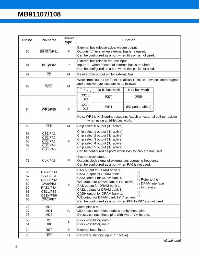
80 BGRNT/P81 FExternal bus release acknowledge output.Outputs “L” level when external bus is released.Can be configured as a port when this pin is not used.
81 BRQ/P82 PExternal bus release request input.Inputs “1” when release of external bus is required.Can be configured as a port when this pin is not used.
82 RD M Read strobe output pin for external bus.
83 WR0 M
Write strobe output pin for external bus. Relation between control signals and effective byte locations is as follows:
Note: WR1 is Hi-Z during resetting. Attach an external pull-up resister when using at 16-bit bus width.
84 WR1/P85 F
65 CS0 M Chip select 0 output (“L” active).
6667686970
CS1/PA1CS2/PA2CS3/PA3CS4/PA4CS5/PA5
F
Chip select 1 output (“L” active).Chip select 2 output (“L” active).Chip select 3 output (“L” active).Chip select 4 output (“L” active).Chip select 5 output (“L” active).Can be configured as ports when PA1 to PA5 are not used.
71 CLK/PA6 FSystem clock output.Outputs clock signal of external bus operating frequency.Can be configured as a port when PA6 is not used.
5657585960616263
RAS0/PB0CS0L/PB1CS0H/PB2DW0/PB3RAS1/PB4CS1L/PB5CS1H/PB6DW1/PB7
F
RAS output for DRAM bank 0.CASL output for DRAM bank 0.CASH output for DRAM bank 0.WE output for DRAM bank 0 (“L” active).RAS output for DRAM bank 1.CASL output for DRAM bank 1.CASH output for DRAM bank 1.WE output for DRAM bank 1 (“L” active)Can be configured as a port when PB0 to PB7 are not used.
767778
MD0MD1MD2
GMode pins 0 to 2.MCU basic operation mode is set by these pins.Directly connect these pins with VCC or VSS for use.
5354
X1X0
AClock (oscillator) output.Clock (oscillator) input.
74 RST B External reset input.
73 HST H Hardware standby input (“L” active).
16-bit bus width 8-bit bus width
D31 to D24
WR0 WR0
D23 to D16
WR1 (I/O port enabled)
Refer to the DRAM interface for details.

MB91107/108
(Continued)
Pin no. Pin nameCircuit type
Function
72 NMI H NMI (non-maskable interrupt pin) input (“L” active).
42 SC2/PE0 F
(SC2) Clock I/O pin for UART2.Clock output is available when clock output of UART2 is enabled.
(PE0) General purpose I/O port.This function is available when UART2 clock output is disabled.
43 DREQ0/PE1 F
(DREQ0) External transfer request input pins for DMA. This pin is used for input when external trigger is selected to cause DMAC operation, and it is necessary to disable output for other functions from this pin unless such output is made intentionally.
(PE1) General purpose I/O port.
44 DACK0/PE2 F
(DACK0) External transfer request acknowledge output pin for DMAC (ch. 0). This function is available when transfer request output for DMAC is enabled.
(PE2) General purpose I/O port.This function is available when transfer request acknowledge output for DMAC or DACK0 output is disabled.
45 EOP0/PE3 F
(EOP0) Can be configured as DMAC EOP OUTPUT (ch.0) when DMAC EOP output is enable.
(PE3) General purpose I/O port.
46 DREQ1/PE4 F
(DREQ1) External transfer request input pins for DMA. This pin is used for input when external trigger is selected to cause DMAC operation, and it is necessary to disable output for other functions from this pin unless such output is made intentionally.
(PE4) General purpose I/O port.
47 DACK1/PE5 F
(DACK1) External transfer request acknowledge output pin for DMAC (ch. 1). This function is available when transfer request output for DMAC is enabled.
(PE5) General purpose I/O port.This function is available when transfer request acknowledge output for DMAC or DACK1 output is disabled.
48 EOP1/PE6 F
(EOP1) Can be configured as DMAC EOP OUTPUT (ch.1) when DMAC EOP output is enable.
(PE6) General purpose I/O port.
49 DREQ2/PE7 F
(DREQ2) External transfer request input pins for DMA.This pin is used for input when external trigger is selected to cause DMAC operation, and it is necessary to disable output for other functions from this pin unless such output is made intentionally.
(PE7) General purpose I/O port.
7
MB91107/108
8
(Continued)
Pin no. Pin nameCircuit type
Function
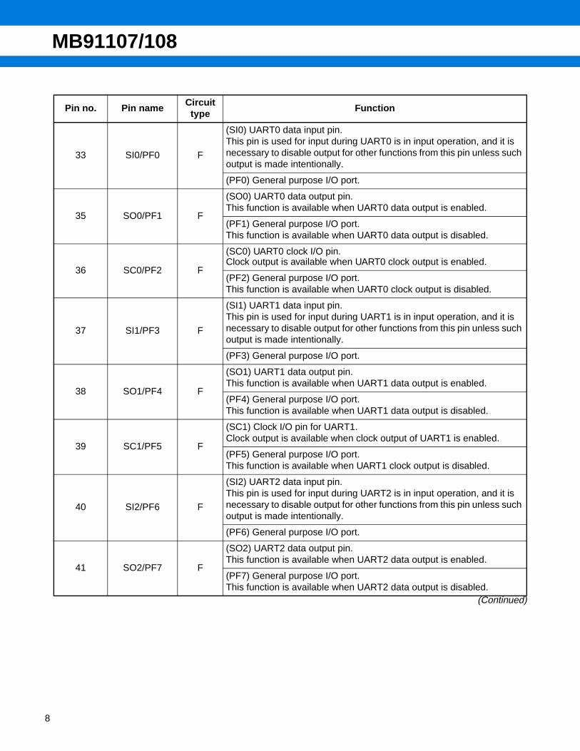
33 SI0/PF0 F
(SI0) UART0 data input pin.This pin is used for input during UART0 is in input operation, and it is necessary to disable output for other functions from this pin unless such output is made intentionally.
(PF0) General purpose I/O port.
35 SO0/PF1 F
(SO0) UART0 data output pin.This function is available when UART0 data output is enabled.
(PF1) General purpose I/O port.This function is available when UART0 data output is disabled.
36 SC0/PF2 F
(SC0) UART0 clock I/O pin.Clock output is available when UART0 clock output is enabled.
(PF2) General purpose I/O port.This function is available when UART0 clock output is disabled.
37 SI1/PF3 F
(SI1) UART1 data input pin.This pin is used for input during UART1 is in input operation, and it is necessary to disable output for other functions from this pin unless such output is made intentionally.
(PF3) General purpose I/O port.
38 SO1/PF4 F
(SO1) UART1 data output pin.This function is available when UART1 data output is enabled.
(PF4) General purpose I/O port.This function is available when UART1 data output is disabled.
39 SC1/PF5 F
(SC1) Clock I/O pin for UART1.Clock output is available when clock output of UART1 is enabled.
(PF5) General purpose I/O port.This function is available when UART1 clock output is disabled.
40 SI2/PF6 F
(SI2) UART2 data input pin.This pin is used for input during UART2 is in input operation, and it is necessary to disable output for other functions from this pin unless such output is made intentionally.
(PF6) General purpose I/O port.
41 SO2/PF7 F
(SO2) UART2 data output pin.This function is available when UART2 data output is enabled.
(PF7) General purpose I/O port.This function is available when UART2 data output is disabled.

MB91107/108
(Continued)
Pin no. Pin nameCircuit type
Function
2526272829303132
INT0/PG0INT1/PG1INT2/PG2INT3/PG3INT4/PG4INT5/PG5INT6/PG6INT7/PG7
I
(INT0 to INT7) External interrupt request input pin.This pin is used for input during corresponding interrupt is enabled, and it is necessary to disable output for other functions from this pin unless such output is made intentionally.
(PG0 and PG7) General purpose I/O port.
1617
TRG0/PH0TRG1/PH1
F(TRG0 and TRG1) PWM timer external trigger input pin. This function is available when PH0 and PH1 data outputs are disabled.
(PH0 and PH1) General purpose I/O port.
1819
TRG2/PH2/CS6
TRG3/PH3/CS7
F
(TRG2 and TRG3) PWM timer external trigger input pin.This function is available when PH2 and PH3 data outputs are disabled.
(PH2 and PH3) Can be configured as a I/O port when TRG2, TRG3, CS6 and CS7 are not used.
Chip select 6 output (“L” active).Chip select 7 output (“L” active).
20212223
OCPA0/PH4OCPA1/PH5OCPA2/PH6OCPA3/PH7
F
(OCPA0 to OCPA3) PWM timer output pin.This function is available when PWM timer output is enabled.
(PH4 to PH7) General purpose I/O port.
50 DACK2/PI0 F
(DACK2) External transfer request acknowledge output pin for DMAC (ch. 2). This function is available when transfer request output for DMAC is enabled.
(PI0) General purpose I/O port.This function is available when transfer request acknowledge output for DMAC or DACK2 output is disabled.
51EOP2/PI1/
ATGF
(EOP2) EOP output pin for DMAC (ch.1).This function is available when EOP output for DMAC is enabled.
(PI1) General purpose I/O port.This function is available when transfer complete acknowledge output for DMAC output is disabled.
(ATG)External trigger input pin for A/D converter.This pin is used for input when external trigger is selected to cause A/D converter operation, and it is necessary to disable output for other func-tions from this pin unless such output is made intentionally.
12 to 15 AN0 to AN3 N(AN0 to AN3) Analog input pins of A/D converter.This function is available when AIC register is set to specify analog input mode.
9 AVCC Power supply pin (VCC) for A/D converter.
10 AVRH Reference voltage input (high) for A/D converter.Make sure to turn on and off this pin with potential of AVRH or more ap-plied to VCC.
9

MB91107/108
10
(Continued)
Note : In most of the above pins, I/O port and resource I/O are multiplexed e.g. xxx/Pxxx. In case of conflict between output of I/O port and resource I/O, priority is always given to the output of resource I/O.
DRAM CONTROL REGISTER
Pin no. Pin nameCircuit type
Function
11 AVSS/ AVRL Power supply pin (VSS) for A/D converter and reference voltage input pin (low).
24, 55, 110
VCC Power supply pin (VCC) for digital circuit.Always three pins must be connected to the power supply
64 C Bypass capacitor pin for internal capacitor.Refer to the HANDLING DEVICES.
34, 52, 75, 101, 119
VSS Earth level (VSS) for digital circuit.
Pin name
Data bus 16-bit mode Data bus 8-bit mode Remarks
2CAS/1WR mode 1CAS/2WR mode
RAS0 Area 4 RAS Area 4 RAS Area 4 RAS Correspondence of “L” “H” to lower ad-dress 1 bit (A0) in data bus 16-bit mode.
“L”: “0”“H”: “1”
CASL : CAS which A0 corresponds to “0” area
CASH : CAS which A0 corresponds to “1” area
WEL : WE which A0 corresponds to “0” area
WEH : WE which A0 corresponds to “1”
RAS1 Area 5 RAS Area 5 RAS Area 5 RAS
CS0L Area 4 CASL Area 4 CAS Area 4 CAS
CS0H Area 4 CASH Area 4 WEL Area 4 CAS
CS1L Area 5 CASL Area 5 CAS Area 5 CAS
CS1H Area 5 CASH Area 5 WEL Area 5 CAS
DW0 Area 4 WE Area 4 WEL Area 4 WE
DW1 Area 5 WE Area 5 WEL Area 5 WE

MB91107/108
I/O CIRCUIT TYPE
(Continued)
Type Circuit Remarks
A
• Oscillation feedback resistance: 1 MΩapprox.
B
• CMOS level Hysteresis inputWithout standby control
• With pull-up resistance
C
• CMOS level I/OWith standby control
N
• Analog input
X1
STANDBYCONTROL
X0
Clock input
VSS
VCC
Diffused resistor
P-channel type Tr.
N-channel type Tr.
Digital input
STANDBYCONTROL
Digital output
Digital input
Digital output
Analog input
11

MB91107/108
12
(Continued)
Type Circuit Remarks
F
• CMOS level output• CMOS level
Hysteresis inputWith standby control
G
• CMOS level inputWithout standby control
H
• CMOS level Hysteresis inputWithout standby control
I
• CMOS level output• CMOS level
Hysteresis inputWithout standby control
STANDBYCONTROL
Digital output
Digital output
Digital input
Digital input
Digital input
Digital input
Digital output
Digital output

MB91107/108
(Continued)
Type Circuit Remarks
M
• CMOS level output
P
• CMOS level output• CMOS level input
With standby control• With pull-down resistance
Digital output
Digital output
STANDBYCONTROL
Pull-down resistor control
Digital output
Digital output
Digital input
13

MB91107/108
14
HANDLING DEVICES1. Preventing Latchup
In CMOS ICs, applying voltage higher than VCC or lower than VSS to input/output pin or applying voltage overrating across VCC and VSS may cause latchup.This phenomenon rapidly increases the power supply current, which may result in thermal breakdown of thedevice. Make sure to prevent the voltage from exceeding the maximum rating.
2. Treatment of Pins
•Treatment of unused pins
Unused pins left open may cause malfunctions. Make sure to connect them to pull-up or pull-down resistors.
•Handling the output pins
Connecting an output pin to the power supply, to another output pin, or to a large-capacitance load may causea large current to flow. Since letting it flow for an extended period of time degrades the device, be careful inusing the device not to exceed the maximum rating.
•Power supply pins
When there are several VCC and VSS pins, each of them is equipotentially connected to its counterpart inside ofthe device, minimizing the risk of malfunctions such as latch up. To further reduce the risk of malfunctions, toprevent EMI radiation, to prevent strobe signal malfunction resulting from creeping-up of ground level and toobserve the total output current standard, connect all VCC and VSS pins to the power supply or GND.It is preferred to connect VCC and VSS of MB91107 to power supply with minimal impedance possible.It is also recommended to connect a ceramic capacitor as a bypass capacitor of about 0.1 µF between VCC andVSS at a position as close as possible to MB91107.
•Mode setting pins (MD0 to MD2)
Connect mode setting pins (MD0 to MD2) directly to VCC or VSS.Arrange each mode setting pin and VCC or VSS patterns on the printed circuit board as close as possible andmake the impedance between them minimal to prevent mistaken entrance to the test mode caused by noises.
•Crystal oscillator circuit
Noises around X0 and X1 pins may cause malfunctions of MB91101. In designing the PC board, layout X0, X1and crystal oscillator (or ceramic oscillator) and bypass capacitor for grounding as close as possible. It is strongly recommended to design PC board so that X1 and X0 pins are surrounded by grounding area forstable operation.
3. Notes on Use
•External reset input
The RST pin requires "L" level input for at least five machine cycles before the the internal circuitry can becompletely reset.
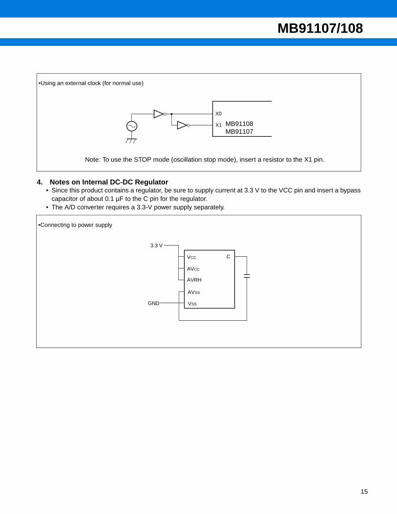
•External clock
To use an external clock, in principle, supply the X0 and X1 pins with a clock signal opposite in phase to the X0.To use the STOP mode (oscillation stop mode) along with the external clock, in which the X1 pin stops with "H"output, you should insert an external resistor of about 1 kilohm to prevent a collision between outputs.Given the next page is an example of using an external clock.
MB91107/108
4. Notes on Internal DC-DC Regulator• Since this product contains a regulator, be sure to supply current at 3.3 V to the VCC pin and insert a bypass
capacitor of about 0.1 µF to the C pin for the regulator.• The A/D converter requires a 3.3-V power supply separately.
•Using an external clock (for normal use)
X0
X1
Note: To use the STOP mode (oscillation stop mode), insert a resistor to the X1 pin.
MB91108MB91107
3.3 V
GND
VCC
AVCC
AVRH
AVSS
VSS
C
•Connecting to power supply
15

MB91107/108
16
•••• Notes on using the STOP mode
The regulator built in this product stops in the STOP mode. If the regulator stops due to a malfunction causedby noise or a fault in the power supply during normal operation, the internal 2.5-V power supply may go belowthe lower limit of the guaranteed operating voltage range. When using the STOP mode with the internal regulator,therefore, be sure to supply an auxiliary external power to prevent the 3.3-V power supply from coming down.Even in that case, the internal regulator can be restarted by input of a reset signal (To restart the regulator, keepthe reset pin at the L level for at least the oscillation settling time).
5. Turning on the Power Supply
•RST pin
When turning on the power supply, never fail to start from setting the RST pin to “L” level. And after the powersupply voltage goes to VCC level, at least after ensuring the time for 5 machine cycles, then set to “H” level.
•Pin Condition at Turning on the Power Supply
The pin condition at turning on the power supply is unstable. The circuit starts being initialized after turning onthe power supply and then starting oscillation and then the operation of the internal regulator becomes stable.So it takes about 42 ms for the pin to be initialized from the oscillation starting at the source oscillation 12.5 MHz.Take care that the pin condition may be output condition at initial unstable condition.(With the MB91107, however, initalization can be achieved in less than about 42 ms after turning on the internalpower supply by maintaining the RST pin at "L" level.)
•Source Oscillation Input at Turning on the Power Supply
At turning on the power supply, never fail to input the clock before cancellation of the oscillation stabilizing waiting.
•Hardware Stand-by at Turning on the Power Supply
When turning on the power supply with the HST pin being set to “L” level, the hardware doesn’t stand by. Howeverthe HST pin becomes available after the reset cancellation, the HST pin must once be back to “H” level.
•Power on Reset
Make sure to make power on reset at turning on the power supply or returning on the power supply when thepower supply voltage is below the warranty range for normal operation.
•Using STOP mode with 3.3 V power supply
3.3 V
VCC
VSS
C
2.4 kΩ
7.6 kΩ0.1 µF
MB91107/108
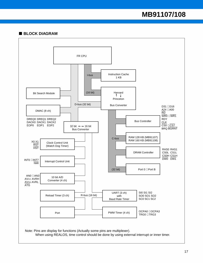
BLOCK DIAGRAM
FR CPU
I-bus
(16 bit)
D-bus (32 bit)
Instruction Cache1 KB
Harvard
Princeton
Bus Converter
Bit Search Module
DMAC (8 ch)
DREQ0DACK0EOP0
DREQ1DACK1EOP1
DREQ2DACK2EOP2 32 bit 16 bit
Bus Converter
X0 X1RSTHST
Clock Control Unit(Watch Dog Timer)
INT0 ∼ INT7NMI
Interrupt Control Unit
AN0 ∼ AN3AVCC AVRHAVSS AVRLATG
10 bit A/DConverter (4 ch)
Reload Timer (3 ch)
Port
R-bus (16 bit)UART (3 ch)
withBaud Rate Timer
PWM Timer (4 ch)
SI0 SI1 SI2SO0 SO1 SO2SC0 SC1 SC2
OCPA0 ∼ OCPA3TRG0 ∼ TRG3
(32 bit)
C-bus
Port 0 ∼ Port B
DRAM Controller
RAM 128 KB (MB91107)RAM 160 KB (MB91108)
Bus Controller
RAS0CS0LCS0HDW0
RAS1CS1LCS1HDW1
D31 ∼ D16A24 ∼ A00RDWR0 ∼ WR1RDYCLKCS0 ∼ CS7BRQ BGRNT
Note: Pins are display for functions (Actually some pins are multiplexer).When using REALOS, time control should be done by using external interrupt or inner timer.
17

MB91107/108
18
CPU CORE1. Memory Space
The FR family has a logical address space of 4 Gbytes (232 bytes) and the CPU linearly accesses the memoryspace.
0000 0000H
0000 0400H
0000 0800H
0001 0000H
000C 0000H
000E 0000H
0010 0000H
FFFF FFFFH
I/O
I/O
I/O
I/O
000E 8000H
Access inhibited
External ROM/external bus mode
Access inhibited
Direct addressing area*1
See “ I/O MAP”
*1: The following areas on the memory space are assigned to direct addressing area forI/O. In these areas, an address can be specified in a direct operand of a code.Direct areas consists of the following areas dependent on accessible data sizes.
*2: Access inhibited of MB91107
Note : Only the above mode exist in this product.
→ byte data access 0-0FFH
→ half word data access 0-1FFH
→ word data access 0-3FFH
External areaExternal area
Internal RAMExternal areaInternal RAM
External areaExternal area
←Internal 32KB-RAM *2 (MB91108 only)
←Internal 128 KB-RAM
Internal ROM/external bus mode
Access inhibited
MB91107/108
2. Registers
The FR family has two types of registers; dedicated registers embedded on the CPU and general-purposeregisters on memory.
•Dedicated registers
•Program status (PS)
The PS register is for holding program status and consists of a condition code register (CCR), a system conditioncode register (SCR) and a interrupt level mask register (ILM).
Program counter (PC) : 32-bit length, indicates the location of the instruction to be executed.Program status (PS) : 32-bit length, register for storing register pointer or condition codes.
Table base register (TBR) : Holds top address of vector table used in EIT (Exceptional/Interrupt/
Trap processing.Return pointer (RP) : Holds address to resume operation after returning from a subroutine.System stack pointer (SSP) : Indicates system stack space.User's stack pointer (USP) : Indicates user’s stack space.Multiplication/division result register (MDH/MDL)
: 32-bit length, register for multiplication/division.
32 bit 32 bit Initial value
Program counter PC XXXX XXXX Indeterminate
Program status PS ILM SCR CCR
Table base register TBR 0 0 0F FC 0 0
Return pointer RP XXXX XXXX Indeterminate
System stack pointer SSP 0 0 0 0 0 0 0 0
User’s stack pointer USP XXXX XXXX Indeterminate
Multiplication/division re-sult register
MDH XXXX XXXX Indeterminate
MDL XXXX XXXX Indeterminate
31 20 19 18 17 16 10 9 8 7 6 5 4 3 2 1 0
PS ILM4 to ILM0 D1 D0 T S I N Z V C
ILM SCR CCR
19

MB91107/108
20
•Condition code register (CCR)
•System condition code register (SCR)
•Interrupt level mask register (ILM)
S-flag : Specifies a stack pointer used as R15.I-flag : Controls user interrupt request enable/disable.N-flag : Indicates sign bit when division result is assumed to be in the 2’s complement format.Z-flag : Indicates whether or not the result of division was “0”.
V-flag: Assumes the operand used in calculation in the 2’s complement format and indicates whether or not overflow has occurred.
C-flag : Indicates if a carry or borrow from the MSB has occurred.
T-flag : Specifies whether or not to enable step trace trap.
ILM4 to ILM0 : Register for holding interrupt level mask value. The value held by this register is used as a level mask. When an interrupt request issued to the CPU is higher than the level held by ILM, the interrupt request is accepted.
ILM4 ILM3 ILM2 ILM1 ILM0 Interrupt level High-low
0 0 0 0 0 0 High
0 1 1 1 1 15
1 1 1 1 1 31 Low

MB91107/108
GENERAL-PURPOSE REGISTERSR0 to R15 are general-purpose registers embedded on the CPU. These registers functions as an accumulatorand a memory access pointer.
Of the above 16 registers, following registers have special functions. To support the special functions, part ofthe instruction set has been sophisticated to have enhanced functions.
R13: Virtual accumulator (AC)R14: Frame pointer (FP)R15: Stack pointer (SP)
Upon reset, values in R0 to R14 are not fixed. Value in R15 is initialized to be 0000 0000H (SSP value).
32 bit Initial valueR0 XXXX XXXXH
R1 ::
: : ::
R12 :R13 AC :R14 FP XXXX XXXXH
R15 SP 0000 0000H
21
MB91107/108
22
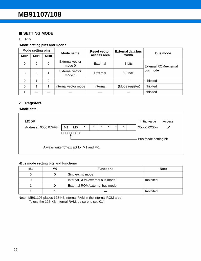
SETTING MODE1. Pin
•Mode setting pins and modes
2. Registers
•Mode data
•Bus mode setting bits and functions
Note : MB91107 places 128-KB internal RAM in the internal ROM area.To use the 128-KB internal RAM, be sure to set ’01’.
Mode setting pinsMode name Reset vector
access areaExternal data bus
width Bus modeMD2 MD1 MD0
0 0 0External vector
mode 0External 8 bits
External ROM/external bus mode
0 0 1External vector
mode 1External 16 bits
0 1 0 — — — Inhibited
0 1 1 Internal vector mode Internal (Mode register) Inhibited
1 — — — — — Inhibited
M1 M0 Functions Note
0 0 Single-chip mode
0 1 Internal ROM/external bus mode Inhibited
1 0 External ROM/external bus mode
1 1 — Inhibited
MODR Initial value Access
Address : 0000 07FFH M1 M0 ∗ ∗ ∗ ∗ ∗ ∗ XXXX XXXXB W
Bus mode setting bit
Always write “0” except for M1 and M0.
MB91107/108
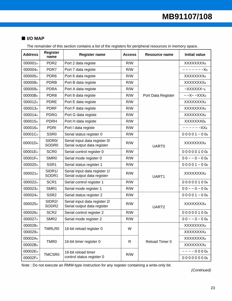
I/O MAP
The remainder of this section contains a list of the registers for peripheral resources in memory space.
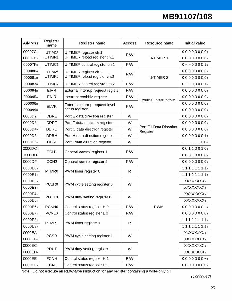
Note : Do not execute an RMW-type instruction for any register containing a write-only bit.(Continued)
Address Register name Register name Access Resource name Initial value
000001H PDR2 Port 2 data registe R/W
Port Data Register
XXXXXXXXB
000004H PDR7 Port 7 data registe R/W − − − − − − −XB
000005H PDR6 Port 6 data registe R/W XXXXXXXXB
000008H PDRB Port B data registe R/W XXXXXXXXB
000009H PDRA Port A data registe R/W −XXXXXX−B
00000BH PDR8 Port 8 data registe R/W − −X− −XXXB
000012H PDRE Port E data registe R/W XXXXXXXXB
000013H PDRF Port F data registe R/W XXXXXXXXB
000014H PDRG Port G data registe R/W XXXXXXXXB
000015H PDRH Port H data registe R/W XXXXXXX0B
000016H PDRI Port I data registe R/W − − − − − −XXB
00001CH SSR0 Serial status register 0 R/W
UART0
0 0 0 0 1 − 0 0B
00001DHSIDR0/SODR0
Serial input data register 0/Serial output data register
R/W XXXXXXXXB
00001EH SCR0 Serial control register 0 R/W 0 0 0 0 0 1 0 0B
00001FH SMR0 Serial mode register 0 R/W 0 0 − − 0 − 0 0B
000020H SSR1 Serial status register 1 R/W
UART1
0 0 0 0 1 − 0 0B
000021HSIDR1/SODR1
Serial input data register 1/Serial output data register
R/W XXXXXXXXB
000022H SCR1 Serial control register 1 R/W 0 0 0 0 0 1 0 0B
000023H SMR1 Serial mode register 1 R/W 0 0 − − 0 − 0 0B
000024H SSR2 Serial status register 2 R/W
UART2
0 0 0 0 1 − 0 0B
000025HSIDR2/SODR2
Serial input data register 2/Serial output data register
R/W XXXXXXXXB
000026H SCR2 Serial control register 2 R/W 0 0 0 0 0 1 0 0B
000027H SMR2 Serial mode register 2 R/W 0 0 − − 0 − 0 0B
000028HTMRLR0 16-bit reload register 0 W
Reload Timer 0
XXXXXXXXB
000029H XXXXXXXXB
00002AHTMR0 16-bit timer register 0 R
XXXXXXXXB
00002BH XXXXXXXXB
00002EHTMCSR0
16-bit reload timer control status register 0
R/W− − − − 0 0 0 0B
00002FH 0 0 0 0 0 0 0 0B
23

MB91107/108
24
Note : Do not execute an RMW-type instruction for any register containing a write-only bit.(Continued)
Address Register name Register name Access Resource name Initial value
000030HTMRLR1 16-bit reload register 1 W
Reload Timer 1
XXXXXXXXB
000031H XXXXXXXXB
000032HTMR1 16-bit timer register 1 R
XXXXXXXXB
000033H XXXXXXXXB
000036HTMCSR1
16-bit reload timer control status register 1
R/W− − − − 0 0 0 0B
000037H 0 0 0 0 0 0 0 0B
000038HADCR A/D converter data register R A/D Converter
(Successive approximation type)
− − − − − − XXB
000039H XXXXXXXXB
00003AHADCS A/D converte control status register R/W
0 0 0 0 0 0 0 0B
00003BH 0 0 0 0 0 0 0 0B
00003CHTMRLR2 16-bit reload register 2 W
Reload Timer 2
XXXXXXXXB
00003DH XXXXXXXXB
00003EHTMR2 16-bit timer register 2 R
XXXXXXXXB
00003FH XXXXXXXXB
000042HTMCSR2
16-bit reload timer control status register 2
R/W− − − − 0 0 0 0B
000043H 0 0 0 0 0 0 0 0B
000050HASR6 Area select register 6 W
External Bus Interface
1 1 1 1 1 1 1 1B
000051H 1 1 1 1 1 1 1 1B
000052HAMR6 Area mask register 6 W
0 0 0 0 0 0 0 0B
000053H 0 0 0 0 0 0 0 0B
000054HASR7 Area select register 7 W
1 1 1 1 1 1 1 1B
000055H 1 1 1 1 1 1 1 1B
000056HAMR7 Area mask register 7 W
0 0 0 0 0 0 0 0B
000057H 0 0 0 0 0 0 0 0B
000059H CS67 Output enable R/W − − − − 0 0 1 1B
000078H UTIM0/UTIMR0
U-TIMER register ch.0U-TIMER reload register ch.0
R/WU-TIMER 0
0 0 0 0 0 0 0 0B
000079H 0 0 0 0 0 0 0 0B
00007BH UTIMC0 U-TIMER control register ch.0 R/W 0 − − 0 0 0 0 1B
MB91107/108
Note : Do not execute an RMW-type instruction for any register containing a write-only bit.(Continued)
Address Register name Register name Access Resource name Initial value
00007CH UTIM1/UTIMR1
U-TIMER register ch.1U-TIMER reload register ch.1
R/WU-TIMER 1
0 0 0 0 0 0 0 0B
00007DH 0 0 0 0 0 0 0 0B
00007FH UTIMC1 U-TIMER control register ch.1 R/W 0 − − 0 0 0 0 1B
000080H UTIM2/UTIMR2
U-TIMER register ch.2U-TIMER reload register ch.2
R/WU-TIMER 2
0 0 0 0 0 0 0 0B
000081H 0 0 0 0 0 0 0 0B
000083H UTIMC2 U-TIMER control register ch.2 R/W 0 − − 0 0 0 0 1B
000094H EIRR External interrup request register R/W
External Interrupt/NMI
0 0 0 0 0 0 0 0B
000095H ENIR Interrupt enabble register R/W 0 0 0 0 0 0 0 0B
000098HELVR External interrup request level
setup registerR/W
0 0 0 0 0 0 0 0B
000099H 0 0 0 0 0 0 0 0B
0000D2H DDRE Port E data direction register W
Port E-I Data Direction Register
0 0 0 0 0 0 0 0B
0000D3H DDRF Port F data direction register W 0 0 0 0 0 0 0 0B
0000D4H DDRG Port G data direction register W 0 0 0 0 0 0 0 0B
0000D5H DDRH Port H data direction register W 0 0 0 0 0 0 0 1B
0000D6H DDRI Port I data direction register W − − − − − − 0 0B
0000DCHGCN1 General control register 1 R/W
PWM
0 0 1 1 0 0 1 0B
0000DDH 0 0 0 1 0 0 0 0B
0000DFH GCN2 General control register 2 R/W 0 0 0 0 0 0 0 0B
0000E0HPTMR0 PWM timer register 0 R
1 1 1 1 1 1 1 1B
0000E1H 1 1 1 1 1 1 1 1B
0000E2HPCSR0 PWM cycle setting register 0 W
XXXXXXXXB
0000E3H XXXXXXXXB
0000E4HPDUT0 PWM duty setting register 0 W
XXXXXXXXB
0000E5H XXXXXXXXB
0000E6H PCNH0 Control status register H 0 R/W 0 0 0 0 0 0 0 −B
0000E7H PCNL0 Control status register L 0 R/W 0 0 0 0 0 0 0 0B
0000E8HPTMR1 PWM timer register 1 R
1 1 1 1 1 1 1 1B
0000E9H 1 1 1 1 1 1 1 1B
0000EAHPCSR PWM cycle setting register 1 W
XXXXXXXXB
0000EBH XXXXXXXXB
0000ECHPDUT PWM duty setting register 1 W
XXXXXXXXB
0000EDH XXXXXXXXB
0000EEH PCNH Control status register H 1 R/W 0 0 0 0 0 0 0 −B
0000EFH PCNL Control status register L 1 R/W 0 0 0 0 0 0 0 0B
25

MB91107/108
26
Note : Do not execute an RMW-type instruction for any register containing a write-only bit.(Continued)
Address Register name Register name Access Resource name Initial value
0000F0HPTMR2 PWM timer register 2 R
PWM
1 1 1 1 1 1 1 1B
0000F1H 1 1 1 1 1 1 1 1B
0000F2HPCSR2 PWM cycle setting register 2 W
XXXXXXXXB
0000F3H XXXXXXXXB
0000F4HPDUT2 PWM duty setting register 2 W
XXXXXXXXB
0000F5H XXXXXXXXB
0000F6H PCNH2 Control status register H 2 R/W 0 0 0 0 0 0 0 −B
0000F7H PCNL2 Control status register L 2 R/W 0 0 0 0 0 0 0 0B
0000F8HPTMR3 PWM timer register 3 R
1 1 1 1 1 1 1 1B
0000F9H 1 1 1 1 1 1 1 1B
0000FAHPCSR3 PWM cycle setting register 3 W
XXXXXXXXB
0000FBH XXXXXXXXB
0000FCHPDUT3 PWM duty setting register 3 W
XXXXXXXXB
0000FDH XXXXXXXXB
0000FEH PCNH3 Control status register H 3 R/W 0 0 0 0 0 0 0 −B
0000FFH PCNL3 Control status register L 3 R/W 0 0 0 0 0 0 0 0B
000200H
DPDP DMAC parameter descriptor point R/W
DMAC
XXXXXXXXB
000201H XXXXXXXXB
000202H XXXXXXXXB
000203H X 0 0 0 0 0 0 0B
000204H
DACSR DMAC control status register R/W
0 0 0 0 0 0 0 0B
000205H 0 0 0 0 0 0 0 0B
000206H 0 0 0 0 0 0 0 0B
000207H 0 0 0 0 0 0 0 0B
000208H
DATCR DMAC pin control register R/W
XXXXXXXXB
000209H XX 0 0 0 0 0 0B
00020AH XX 0 0 0 0 0 0B
00020BH XX 0 0 0 0 0 0B
0003E4H
ICHCR Instruction cache R/W Instruction Cache
− − − − − − − −B
0003E5H − − − − − − − −B
0003E6H − − − − − − − −B
0003E7H − − 0 0 0 0 0 0B
MB91107/108
Note : Do not execute an RMW-type instruction for any register containing a write-only bit.(Continued)
Address Register name Register name Access Resource name Initial value
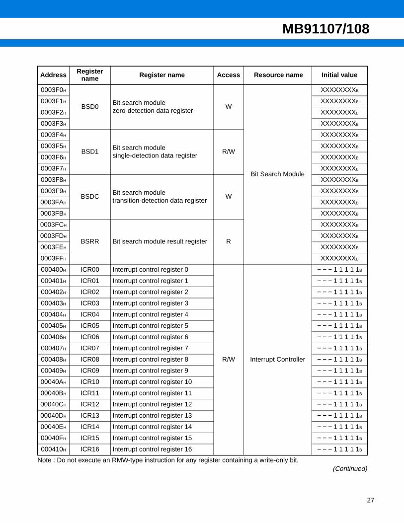
0003F0H
BSD0Bit search module zero-detection data register
W
Bit Search Module
XXXXXXXXB
0003F1H XXXXXXXXB
0003F2H XXXXXXXXB
0003F3H XXXXXXXXB
0003F4H
BSD1Bit search module single-detection data register
R/W
XXXXXXXXB
0003F5H XXXXXXXXB
0003F6H XXXXXXXXB
0003F7H XXXXXXXXB
0003F8H
BSDCBit search module transition-detection data register
W
XXXXXXXXB
0003F9H XXXXXXXXB
0003FAH XXXXXXXXB
0003FBH XXXXXXXXB
0003FCH
BSRR Bit search module result register R
XXXXXXXXB
0003FDH XXXXXXXXB
0003FEH XXXXXXXXB
0003FFH XXXXXXXXB
000400H ICR00 Interrupt control register 0
R/W Interrupt Controller
− − − 1 1 1 1 1B
000401H ICR01 Interrupt control register 1 − − − 1 1 1 1 1B
000402H ICR02 Interrupt control register 2 − − − 1 1 1 1 1B
000403H ICR03 Interrupt control register 3 − − − 1 1 1 1 1B
000404H ICR04 Interrupt control register 4 − − − 1 1 1 1 1B
000405H ICR05 Interrupt control register 5 − − − 1 1 1 1 1B
000406H ICR06 Interrupt control register 6 − − − 1 1 1 1 1B
000407H ICR07 Interrupt control register 7 − − − 1 1 1 1 1B
000408H ICR08 Interrupt control register 8 − − − 1 1 1 1 1B
000409H ICR09 Interrupt control register 9 − − − 1 1 1 1 1B
00040AH ICR10 Interrupt control register 10 − − − 1 1 1 1 1B
00040BH ICR11 Interrupt control register 11 − − − 1 1 1 1 1B
00040CH ICR12 Interrupt control register 12 − − − 1 1 1 1 1B
00040DH ICR13 Interrupt control register 13 − − − 1 1 1 1 1B
00040EH ICR14 Interrupt control register 14 − − − 1 1 1 1 1B
00040FH ICR15 Interrupt control register 15 − − − 1 1 1 1 1B
000410H ICR16 Interrupt control register 16 − − − 1 1 1 1 1B
27

MB91107/108
28
Note : Do not execute an RMW-type instruction for any register containing a write-only bit.(Continued)
Address Register name Register name Access Resource name Initial value
000411H ICR17 Interrupt control register17
R/W Interrupt Controller
− − − 1 1 1 1 1B
000412H ICR18 Interrupt control register 18 − − − 1 1 1 1 1B
000413H ICR19 Interrupt control register 19 − − − 1 1 1 1 1B
000414H ICR20 Interrupt control register 20 − − − 1 1 1 1 1B
000415H ICR21 Interrupt control register 21 − − − 1 1 1 1 1B
000416H ICR22 Interrupt control register 22 − − − 1 1 1 1 1B
000417H ICR23 Interrupt control register 23 − − − 1 1 1 1 1B
000418H ICR24 Interrupt control register 24 − − − 1 1 1 1 1B
000419H ICR25 Interrupt control register 25 − − − 1 1 1 1 1B
00041AH ICR26 Interrupt control register 26 − − − 1 1 1 1 1B
00041BH ICR27 Interrupt control register 27 − − − 1 1 1 1 1B
00041CH ICR28 Interrupt control register 28 − − − 1 1 1 1 1B
00041DH ICR29 Interrupt control register 29 − − − 1 1 1 1 1B
00041EH ICR30 Interrupt control register 30 − − − 1 1 1 1 1B
00041FH ICR31 Interrupt control register 31 − − − 1 1 1 1 1B
000420H ICR32 Interrupt control register 32 − − − 1 1 1 1 1B
000421H ICR33 Interrupt control register 33 − − − 1 1 1 1 1B
000422H ICR34 Interrupt control register 34 − − − 1 1 1 1 1B
000423H ICR35 Interrupt control register 35 − − − 1 1 1 1 1B
000424H ICR36 Interrupt control register 36 − − − 1 1 1 1 1B
000425H ICR37 Interrupt control register 37 − − − 1 1 1 1 1B
000426H ICR38 Interrupt control register 38 − − − 1 1 1 1 1B
000427H ICR39 Interrupt control register 39 − − − 1 1 1 1 1B
000428H ICR40 Interrupt control register 40 − − − 1 1 1 1 1B
000429H ICR41 Interrupt control register 41 − − − 1 1 1 1 1B
00042AH ICR42 Interrupt control register 42 − − − 1 1 1 1 1B
00042BH ICR43 Interrupt control register 43 − − − 1 1 1 1 1B
00042CH ICR44 Interrupt control register 44 − − − 1 1 1 1 1B
00042DH ICR45 Interrupt control register 45 − − − 1 1 1 1 1B
00042EH ICR46 Interrupt control register 46 − − − 1 1 1 1 1B
00042FH ICR47 Interrupt control register 47 − − − 1 1 1 1 1B
000430H DICR Delayed interrupt R/WDelayed Interrupt Controller Register
− − − − − − − 0B
000431H HRCLHolding request withdrawal request level set register
R/W − − − 1 1 1 1 1B

MB91107/108
Note : Do not execute an RMW-type instruction for any register containing a write-only bit.(Continued)
Address Register name Register name Access Resource name Initial value
000480HRSRR/WTCR
Reset cause register/watchdog cycle control register
R/W
Clock Controller
1 XXXX − 0 0B
000481H STCR Stand-by controller register R/W 0 0 0 1 1 1 − −B
000482H PDRRDMA controller request prohibit resister
R/W − − − − 0 0 0 0B
000483H CTBR Timebase timer clear register W XXXXXXXXB
000484H GCR Gear controller register R/W 1 1 0 0 1 1 − 1B
000485H WPRWatchdog reset generation postpone register
W XXXXXXXXB
000488H PCTR PLL controller register W PLL Controller 0 0 − − 0 − − −B
000601H DDR2 Port 2 data direction register W
Port Direction Register
0 0 0 0 0 0 0 0B
000604H DDR7 Port 7 data direction register W − − − − − − − 0B
000605H DDR6 Port 6 data direction register W 0 0 0 0 0 0 0 0B
000608H DDRB Port B data direction register W 0 0 0 0 0 0 0 0B
000609H DDRA Port A data direction register W − 0 0 0 0 0 0 −B
00060BH DDR8 Port 8 data direction register W − −0 0 0 0 0 0B
00060CHASR1 Area selection register 1 W
External Bus Interface
0 0 0 0 0 0 0 0B
00060DH 0 0 0 0 0 0 0 1B
00060EHAMR1 Area mask register 1 W
0 0 0 0 0 0 0 0B
00060FH 0 0 0 0 0 0 0 0B
000610HASR2 Area selection register 2 W
0 0 0 0 0 0 0 0B
000611H 0 0 0 0 0 0 1 0B
000612HAMR2 Area mask register 2 W
0 0 0 0 0 0 0 0B
000613H 0 0 0 0 0 0 0 0B
000614HASR3 Area selection register 3 W
0 0 0 0 0 0 0 0B
000615H 0 0 0 0 0 0 11B
000616HAMR3 Area mask register 3 W
0 0 0 0 0 0 0 0B
000617H 0 0 0 0 0 0 0 0B
000618HASR4 Area selection register 4 W
0 0 0 0 0 0 0 0B
000619H 0 0 0 0 0 1 0 0B
00061AHAMR4 Area mask register 4 W
0 0 0 0 0 0 0 0B
00061BH 0 0 0 0 0 0 0 0B
00061CHASR5 Area selection register 5 W
0 0 0 0 0 0 0 0B
00061DH 0 0 0 0 0 1 0 1B
29
MB91107/108
30
(Continued)
Note: Do not execute an RMW-type instruction for any register containing a write-only bit.
Note : RMW-type instructions (RMW: Read modify write)
Address Register name Register name Access Resource name Initial value
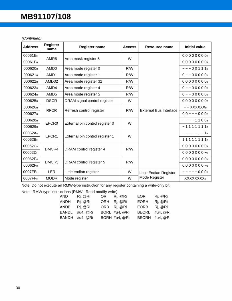
00061EHAMR5 Area mask register 5 W
External Bus Interface
0 0 0 0 0 0 0 0B
00061FH 0 0 0 0 0 0 0 0B
000620H AMD0 Area mode register 0 R/W − − − 0 0 1 1 1B
000621H AMD1 Area mode register 1 R/W 0 − − 0 0 0 0 0B
000622H AMD32 Area mode register 32 R/W 0 0 0 0 0 0 0 0B
000623H AMD4 Area mode register 4 R/W 0 − − 0 0 0 0 0B
000624H AMD5 Area mode register 5 R/W 0 − − 0 0 0 0 0B
000625H DSCR DRAM signal control register W 0 0 0 0 0 0 0 0B
000626HRFCR Refresh control register R/W
− − XXXXXXB
000627H 0 0 − − − 0 0 0B
000628HEPCR0 External pin control register 0 W
− − − − 1 1 0 0B
000629H − 1 1 1 1 1 1 1B
00062AHEPCR1 External pin control register 1 W
− − − − − − − 1B
00062BH 1 1 1 1 1 1 1 1B
00062CHDMCR4 DRAM control register 4 R/W
0 0 0 0 0 0 0 0B
00062DH 0 0 0 0 0 0 0 −B
00062EHDMCR5 DRAM control register 5 R/W
0 0 0 0 0 0 0 0B
00062FH 0 0 0 0 0 0 0 −B
0007FEH LER Little endian register W Little Endian Registor Mode Register
− − − − − 0 0 0B
0007FFH MODR Mode register W XXXXXXXXB
AND Rj, @Ri OR Rj, @Ri EOR Rj, @RiANDH Rj, @Ri ORH Rj, @Ri EORH Rj, @RiANDB Rj, @Ri ORB Rj, @Ri EORB Rj, @RiBANDL #u4, @Ri BORL #u4, @Ri BEORL #u4, @RiBANDH #u4, @Ri BORH #u4, @Ri BEORH #u4, @Ri

MB91107/108
INTERRUPT CAUSES, INTERRUPT VECTORSAND INTERRUPT CONTROL REGISTER ALLOCATIONS
(Continued)
Interrupt causesInterrupt number Interrupt level TBR default
addressDecimal Hexadecimal Register Offset
Reset 0 00 3FCH 0FFFFCH
Reserved for system 1 01 3F8H 0FFFF8H
Reserved for system 2 02 3F4H 0FFFF4H
Reserved for system 3 03 3F0H 0FFFF0H
Reserved for system 4 04 3ECH 0FFFECH
Reserved for system 5 05 3E8H 0FFFE8H
Reserved for system 6 06 3E4H 0FFFE4H
Reserved for system 7 07 3E0H 0FFFE0H
Reserved for system 8 08 3DCH 0FFFDCH
Reserved for system 9 09 3D8H 0FFFD8H
Reserved for system 10 0A 3D4H 0FFFD4H
Reserved for system 11 0B 3D0H 0FFFD0H
Reserved for system 12 0C 3CCH 0FFFCCH
Reserved for system 13 0D 3C8H 0FFFC8H
Exception for undefined instruction 14 0E 3C4H 0FFFC4H
NMI request 15 0F FH fixed 3C0H 0FFFC0H
External interrupt 0 16 10 ICR00 3BCH 0FFFBCH
External interrupt 1 17 11 ICR01 3B8H 0FFFB8H
External interrupt 2 18 12 ICR02 3B4H 0FFFB4H
External interrupt 3 19 13 ICR03 3B0H 0FFFB0H
UART0 receive complete 20 14 ICR04 3ACH 0FFFACH
UART1 receive complete 21 15 ICR05 3A8H 0FFFA8H
UART2 receive complete 22 16 ICR06 3A4H 0FFFA4H
UART0 transmit complete 23 17 ICR07 3A0H 0FFFA0H
UART1 transmit complete 24 18 ICR08 39CH 0FFF9CH
UART2 transmit complete 25 19 ICR09 398H 0FFF98H
DMAC0 (complete, error) 26 1A ICR10 394H 0FFF94H
DMAC1 (complete, error) 27 1B ICR11 390H 0FFF90H
DMAC2 (complete, error) 28 1C ICR12 38CH 0FFF8CH
DMAC3 (complete, error) 29 1D ICR13 388H 0FFF88H
DMAC4 (complete, error) 30 1E ICR14 384H 0FFF84H
DMAC5 (complete, error) 31 1F ICR15 380H 0FFF80H
DMAC6 (complete, error) 32 20 ICR16 37CH 0FFF7CH
DMAC7 (complete, error) 33 21 ICR17 378H 0FFF78H
31
MB91107/108
32
(Continued)
*: When using in REALOS/FR, interrupt 0x40, 0x41 for system code.
Interrupt causesInterrupt number Interrupt level TBR default
addressDecimal Hexadecimal Register Offset
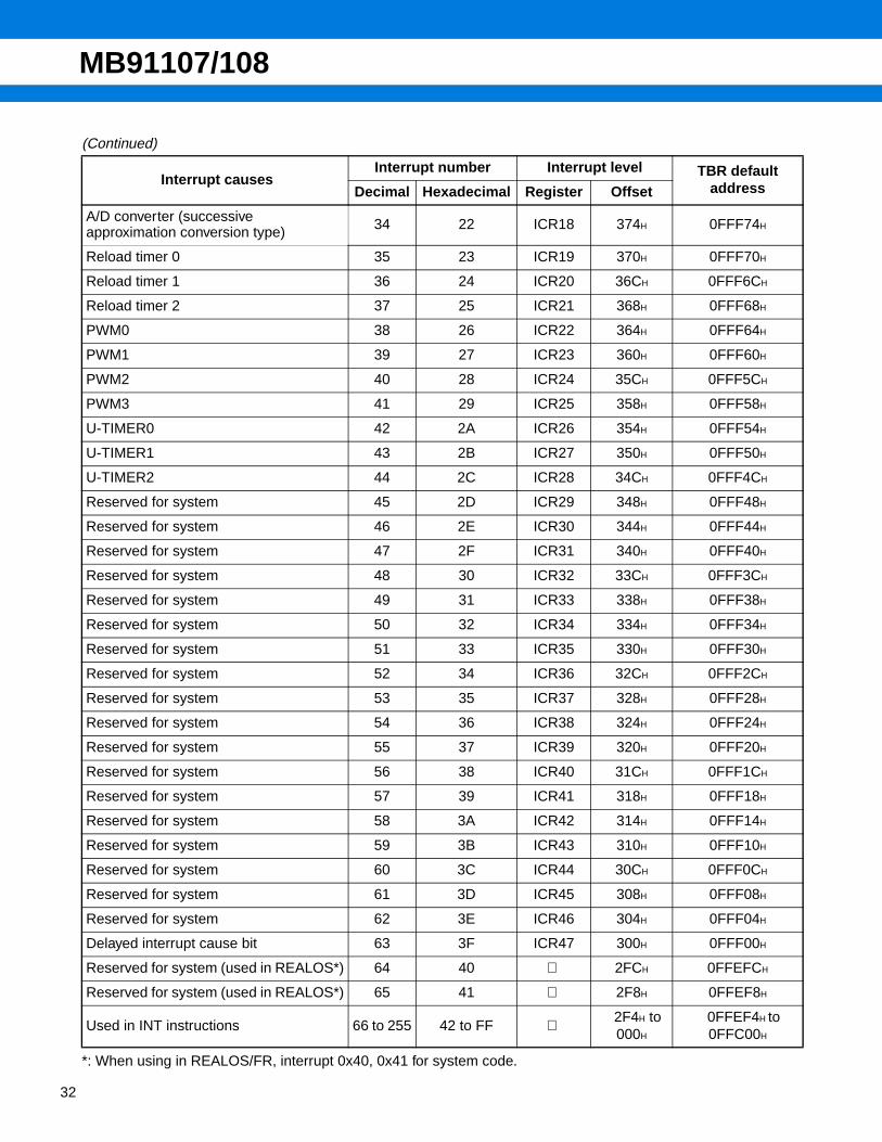
A/D converter (successive approximation conversion type) 34 22 ICR18 374H 0FFF74H
Reload timer 0 35 23 ICR19 370H 0FFF70H
Reload timer 1 36 24 ICR20 36CH 0FFF6CH
Reload timer 2 37 25 ICR21 368H 0FFF68H
PWM0 38 26 ICR22 364H 0FFF64H
PWM1 39 27 ICR23 360H 0FFF60H
PWM2 40 28 ICR24 35CH 0FFF5CH
PWM3 41 29 ICR25 358H 0FFF58H
U-TIMER0 42 2A ICR26 354H 0FFF54H
U-TIMER1 43 2B ICR27 350H 0FFF50H
U-TIMER2 44 2C ICR28 34CH 0FFF4CH
Reserved for system 45 2D ICR29 348H 0FFF48H
Reserved for system 46 2E ICR30 344H 0FFF44H
Reserved for system 47 2F ICR31 340H 0FFF40H
Reserved for system 48 30 ICR32 33CH 0FFF3CH
Reserved for system 49 31 ICR33 338H 0FFF38H
Reserved for system 50 32 ICR34 334H 0FFF34H
Reserved for system 51 33 ICR35 330H 0FFF30H
Reserved for system 52 34 ICR36 32CH 0FFF2CH
Reserved for system 53 35 ICR37 328H 0FFF28H
Reserved for system 54 36 ICR38 324H 0FFF24H
Reserved for system 55 37 ICR39 320H 0FFF20H
Reserved for system 56 38 ICR40 31CH 0FFF1CH
Reserved for system 57 39 ICR41 318H 0FFF18H
Reserved for system 58 3A ICR42 314H 0FFF14H
Reserved for system 59 3B ICR43 310H 0FFF10H
Reserved for system 60 3C ICR44 30CH 0FFF0CH
Reserved for system 61 3D ICR45 308H 0FFF08H
Reserved for system 62 3E ICR46 304H 0FFF04H
Delayed interrupt cause bit 63 3F ICR47 300H 0FFF00H
Reserved for system (used in REALOS*) 64 40 2FCH 0FFEFCH
Reserved for system (used in REALOS*) 65 41 2F8H 0FFEF8H
Used in INT instructions 66 to 255 42 to FF 2F4H to 000H
0FFEF4H to 0FFC00H
MB91107/108
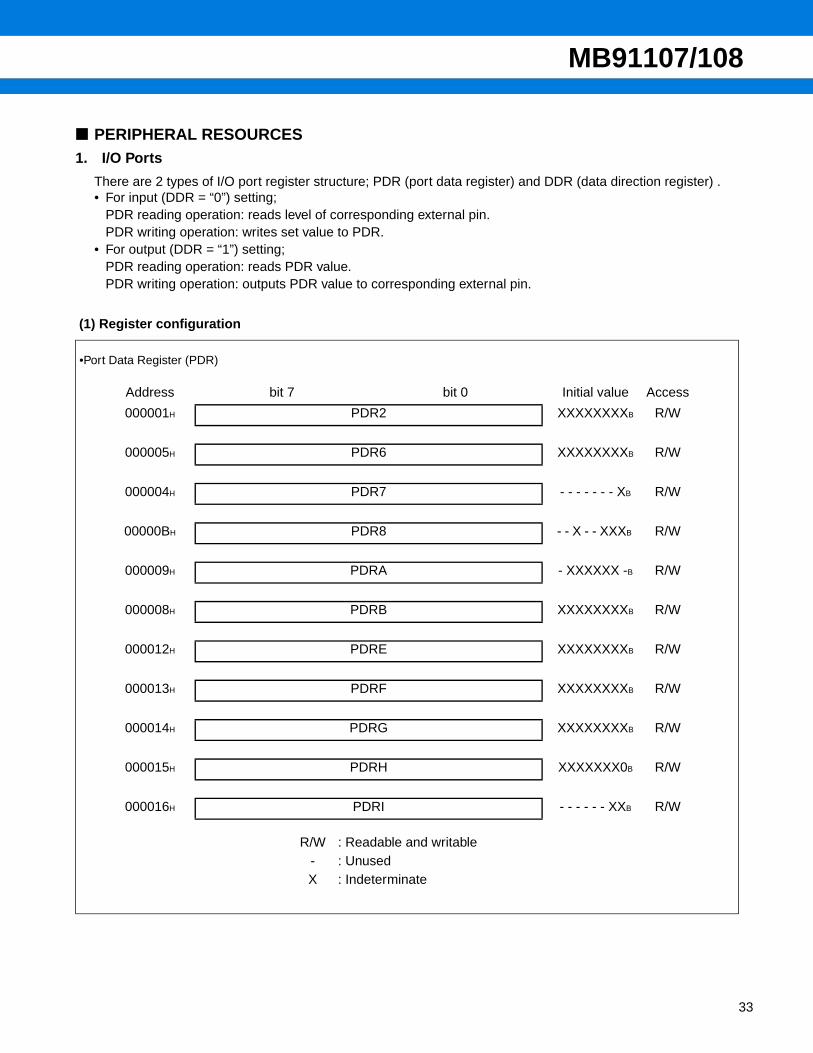
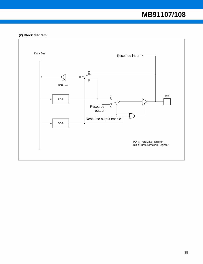
PERIPHERAL RESOURCES1. I/O Ports
There are 2 types of I/O port register structure; PDR (port data register) and DDR (data direction register) .• For input (DDR = “0”) setting;
PDR reading operation: reads level of corresponding external pin.PDR writing operation: writes set value to PDR.
• For output (DDR = “1”) setting;PDR reading operation: reads PDR value.PDR writing operation: outputs PDR value to corresponding external pin.
(1) Register configuration
•Port Data Register (PDR)
Address bit 7 bit 0 Initial value Access
000001H PDR2 XXXXXXXXB R/W
000005H PDR6 XXXXXXXXB R/W
000004H PDR7 - - - - - - - XB R/W
00000BH PDR8 - - X - - XXXB R/W
000009H PDRA - XXXXXX -B R/W
000008H PDRB XXXXXXXXB R/W
000012H PDRE XXXXXXXXB R/W
000013H PDRF XXXXXXXXB R/W
000014H PDRG XXXXXXXXB R/W
000015H PDRH XXXXXXX0B R/W
000016H PDRI - - - - - - XXB R/W
R/W : Readable and writable- : UnusedX : Indeterminate
33
MB91107/108
34
•Data Direction Register (DDR)
Address bit 7 bit 0 Initial value Access
000601H DDR2 0 0 0 0 0 0 0 0B W
000605H DDR6 0 0 0 0 0 0 0 0B W
000604H DDR7 - - - - - - - 0B W
00060BH DDR8 - - 0 - - 0 0 0B W
000609H DDRA - 0 0 0 0 0 0 -B W
000608H DDRB 0 0 0 0 0 0 0 0B W
0000D2H DDRE 0 0 0 0 0 0 0 0B W
0000D3H DDRF 0 0 0 0 0 0 0 0B W
0000D4H DDRG 0 0 0 0 0 0 0 0B W
0000D5H DDRH 0 0 0 0 0 0 0 1B W
0000D6H DDRI - - - - - - 0 0B W
W : Write only- : Unused
MB91107/108
(2) Block diagram
PDR
DDR
1
0
1
0
Data Bus
pin
PDR read
PDR : Port Data RegisterDDR : Data Direction Register
Resource input
Resource output enable
Resourceoutput
35
MB91107/108
36
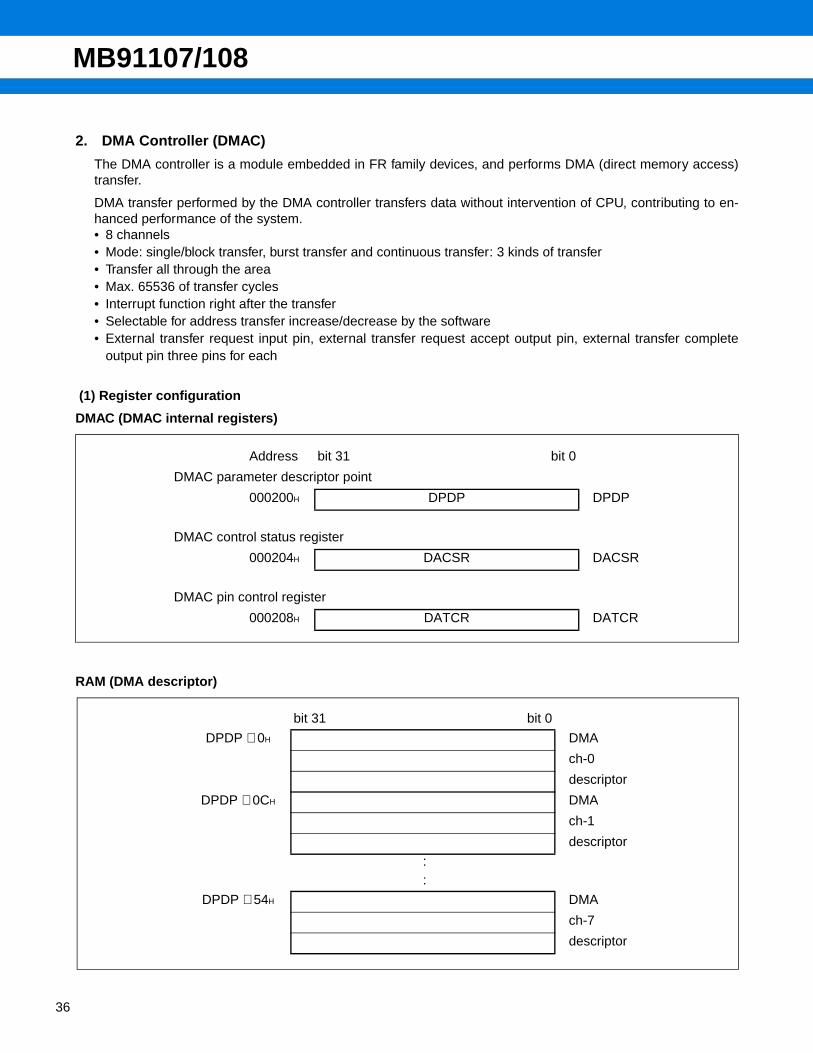
2. DMA Controller (DMAC)
The DMA controller is a module embedded in FR family devices, and performs DMA (direct memory access)transfer.
DMA transfer performed by the DMA controller transfers data without intervention of CPU, contributing to en-hanced performance of the system.• 8 channels• Mode: single/block transfer, burst transfer and continuous transfer: 3 kinds of transfer• Transfer all through the area• Max. 65536 of transfer cycles• Interrupt function right after the transfer• Selectable for address transfer increase/decrease by the software• External transfer request input pin, external transfer request accept output pin, external transfer complete
output pin three pins for each
(1) Register configuration
DMAC (DMAC internal registers)
RAM (DMA descriptor)
Address bit 31 bit 0
DMAC parameter descriptor point
000200H DPDP DPDP
DMAC control status register
000204H DACSR DACSR
DMAC pin control register
000208H DATCR DATCR
bit 31 bit 0
DPDP + 0H DMA
ch-0
descriptor
DPDP + 0CH DMA
ch-1
descriptor
: :
DPDP + 54H DMA
ch-7
descriptor

MB91107/108
(2) Block diagram
DREQ0 ∼DREQ2
DACK0 ∼ DACK2
EOP0 ∼ EOP2
BLK DEC
INC / DEC
BLK
3 3
3
3
8
5
DPDP
DACSR
DATCR
DMACT
SADR
DADR
Edge/leveldetection circuit
Sequencer
SwitcherData buffer
Mode
Data bus
Inner resource Transfer request
Interrupt request
37
MB91107/108
38
3. UART
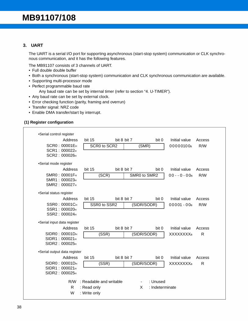
The UART is a serial I/O port for supporting asynchronous (start-stop system) communication or CLK synchro-nous communication, and it has the following features.
The MB91107 consists of 3 channels of UART. • Full double double buffer• Both a synchronous (start-stop system) communication and CLK synchronous communication are available.• Supporting multi-processor mode• Perfect programmable baud rate
Any baud rate can be set by internal timer (refer to section “4. U-TIMER”).• Any baud rate can be set by external clock.• Error checking function (parity, framing and overrun)• Transfer signal: NRZ code• Enable DMA transfer/start by interrupt.
(1) Register configuration
•Serial control register
Address bit 15 bit 8 bit 7 bit 0 Initial value AccessSCR0 :SCR1 :SCR2 :
00001EH
000022H
000026H
SCR0 to SCR2 (SMR) 0 0 0 0 010 0B R/W
•Serial mode register
Address bit 15 bit 8 bit 7 bit 0 Initial value AccessSMR0 :SMR1 :SMR2 :
00001FH
000023H
000027H
(SCR) SMR0 to SMR2 0 0 - - 0 - 0 0B R/W
•Serial status register
Address bit 15 bit 8 bit 7 bit 0 Initial value AccessSSR0 :SSR1 :SSR2 :
00001CH
000020H
000024H
SSR0 to SSR2 (SIDR/SODR) 0 0 0 01 - 0 0B R/W
•Serial input data register
Address bit 15 bit 8 bit 7 bit 0 Initial value AccessSIDR0 :SIDR1 :SIDR2 :
00001DH
000021H
000025H
(SSR) (SIDR/SODR) XXXXXXXXB R
•Serial output data register
Address bit 15 bit 8 bit 7 bit 0 Initial value AccessSIDR0 :SIDR1 :SIDR2 :
00001DH
000021H
000025H
(SSR) (SIDR/SODR) XXXXXXXXB R
R/W : Readable and writable - : UnusedR : Read only X : IndeterminateW : Write only
MB91107/108
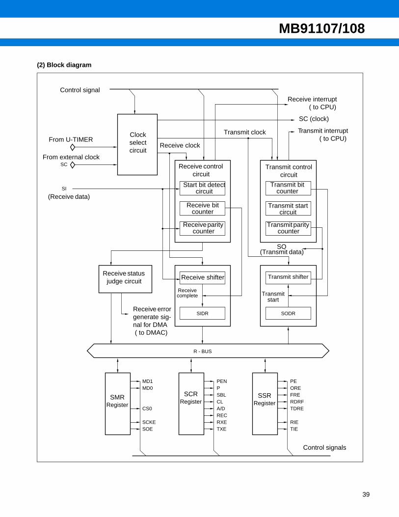
(2) Block diagram
SI
MD1MD0
CS0
SCKESOE
PENPSBLCLA/DRECRXETXE
PEOREFRERDRFTDRE
RIETIE
SC
R - BUS
SIDR SODR
Control signal
From U-TIMER
From external clock
(Receive data)
Clockselectcircuit
Receive status judge circuit
Receive error generate sig-nal for DMA ( to DMAC)
Receive control circuit
Start bit detectcircuit
Receive bit counter
Receive parity counter
Receive shifter
Receive complete
Receive interrupt ( to CPU)
SC (clock)
Transmit interrupt ( to CPU)
Transmit startcircuit
Transmit bit counter
Transmit parity counter
Transmit shifter
Transmitstart
SO (Transmit data)
SMRRegister
Control signals
SCRRegister
SSRRegister
Receive clock
Transmit control circuit
Transmit clock
39
MB91107/108
40
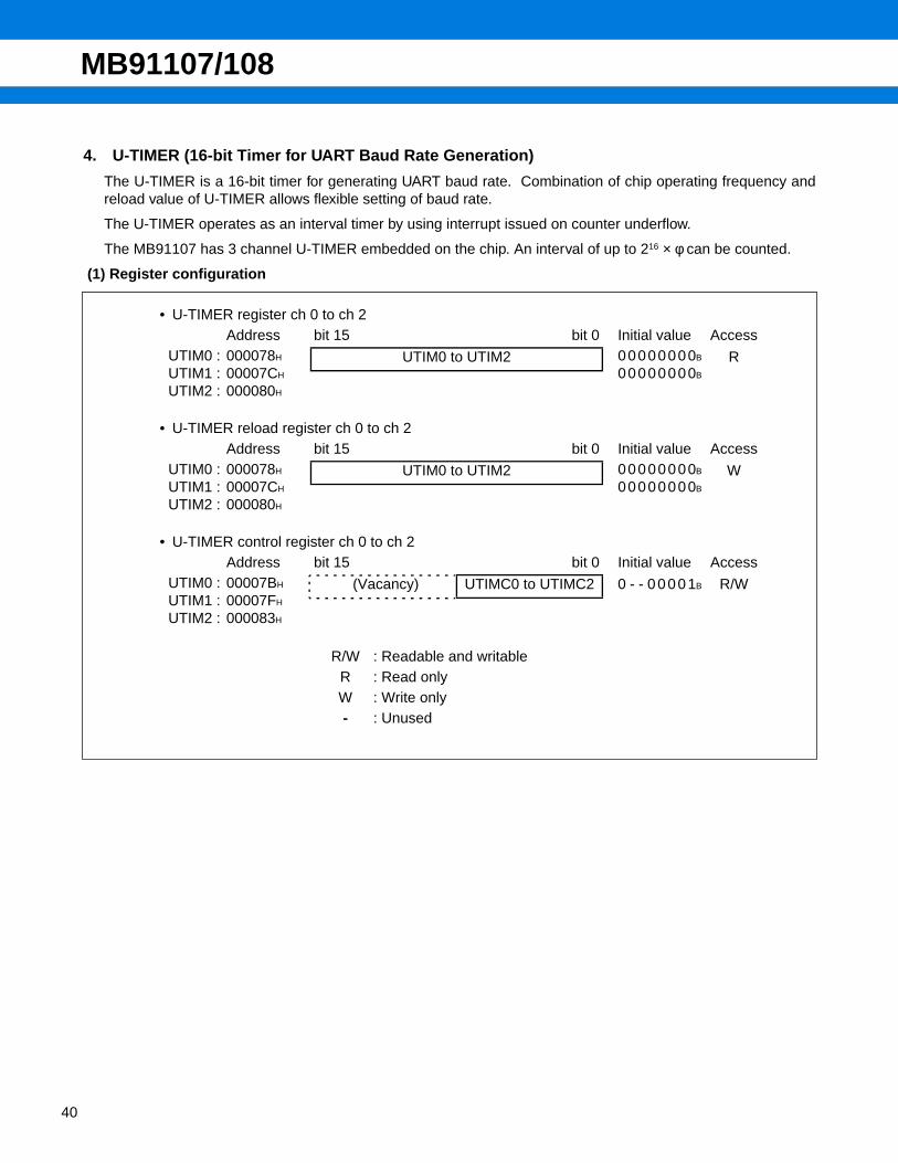
4. U-TIMER (16-bit Timer for UART Baud Rate Generation)
The U-TIMER is a 16-bit timer for generating UART baud rate. Combination of chip operating frequency andreload value of U-TIMER allows flexible setting of baud rate.
The U-TIMER operates as an interval timer by using interrupt issued on counter underflow.
The MB91107 has 3 channel U-TIMER embedded on the chip. An interval of up to 216 × φ can be counted.
(1) Register configuration
• U-TIMER register ch 0 to ch 2Address bit 15 bit 0 Initial value Access
UTIM0 :UTIM1 :UTIM2 :
000078H
00007CH
000080H
UTIM0 to UTIM2 0 0 0 0 0 0 0 0B
0 0 0 0 0 0 0 0B
R
• U-TIMER reload register ch 0 to ch 2Address bit 15 bit 0 Initial value Access
UTIM0 :UTIM1 :UTIM2 :
000078H
00007CH
000080H
UTIM0 to UTIM2 0 0 0 0 0 0 0 0B
0 0 0 0 0 0 0 0B
W
• U-TIMER control register ch 0 to ch 2Address bit 15 bit 0 Initial value Access
UTIM0 :UTIM1 :UTIM2 :
00007BH
00007FH
000083H
(Vacancy) UTIMC0 to UTIMC2 0 - - 0 0 0 0 1B R/W
R/W : Readable and writableR : Read onlyW : Write only- : Unused

MB91107/108
(2) Block diagram
15 0
15 0
φ
f.f.
clock
UTIMR (reload register)
UTIM (timer)
load
underflow
control
to UART
(Peripheral clock)
41

MB91107/108
42
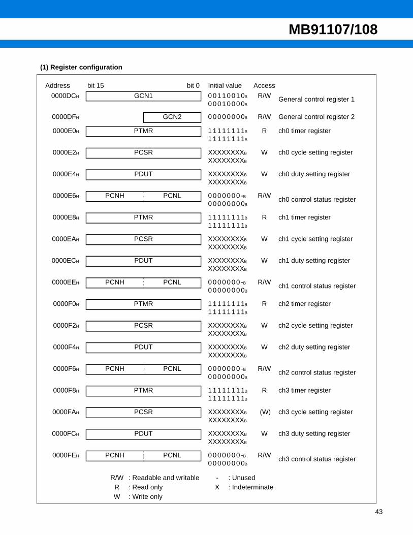
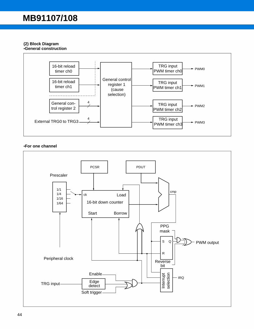
5. PWM Timer
The PWM timer can output high accurate PWM waves efficiently.
MB91101 has inner 4-channel PWM timers, and has the following features.• Each channel consists of a 16-bit down counter, a 16-bit data resister with a buffer for cycle setting, a 16-bit
compare resister with a buffer for duty setting, and a pin controller.• The count clock of a 16-bit down counter can be selected from the following four inner clocks.• Inner clock φ, φ/4, φ/16, φ/64• The counter value can be initialized “FFFFH” by the resetting or the counter borrow.• PWM output (each channel)• Resister description
Cycle setting register: Reload data register with a bufferDuty factor setting register: Compare register with a bufferTransfer from the buffers uses the counter borrow method.
• Pin control outlineSet to ’1’ at a duty factor match. (Preferential)Set to ’0’ at a counter borrow.The output value fixed mode is available, which makes all ’L’ (or ’H’) output easy. The polarity can also be specified.
• Interrupt requests can be generated by selected a combination of events:This timer is activated.A counter borrow is generated (cycle match).A duty factor match is generated.A counter borrow is generated (cycle match) or a duty factor match is generated.
DMA transfer can be invoked by the above interrupt request.• Simultaneous activation of multiple channels of the PWM timer can be set by software or by using another
interval timer. Restarting the PWM timer during operation can also be set.
MB91107/108
(1) Register configuration
Address bit 15 bit 0 Initial value Access
0000DCH GCN1 0 0 1 1 0 0 1 0B
0 0 0 1 0 0 0 0B
R/W General control register 1
0000DFH GCN2 0 0 0 0 0 0 0 0B R/W General control register 2
0000E0H PTMR 1 1 1 1 1 1 1 1B
1 1 1 1 1 1 1 1B
R ch0 timer register
0000E2H PCSR XXXXXXXXB
XXXXXXXXB
W ch0 cycle setting register
0000E4H PDUT XXXXXXXXB
XXXXXXXXB
W ch0 duty setting register
0000E6H PCNH PCNL 0 0 0 0 0 0 0 -B
0 0 0 0 0 0 0 0B
R/W ch0 control status register
0000E8H PTMR 1 1 1 1 1 1 1 1B
1 1 1 1 1 1 1 1B
R ch1 timer register
0000EAH PCSR XXXXXXXXB
XXXXXXXXB
W ch1 cycle setting register
0000ECH PDUT XXXXXXXXB
XXXXXXXXB
W ch1 duty setting register
0000EEH PCNH PCNL 0 0 0 0 0 0 0 -B
0 0 0 0 0 0 0 0B
R/W ch1 control status register
0000F0H PTMR 1 1 1 1 1 1 1 1B
1 1 1 1 1 1 1 1B
R ch2 timer register
0000F2H PCSR XXXXXXXXB
XXXXXXXXB
W ch2 cycle setting register
0000F4H PDUT XXXXXXXXB
XXXXXXXXB
W ch2 duty setting register
0000F6H PCNH PCNL 0 0 0 0 0 0 0 -B
0 0 0 0 0 0 0 0B
R/W ch2 control status register
0000F8H PTMR 1 1 1 1 1 1 1 1B
1 1 1 1 1 1 1 1B
R ch3 timer register
0000FAH PCSR XXXXXXXXB
XXXXXXXXB
(W) ch3 cycle setting register
0000FCH PDUT XXXXXXXXB
XXXXXXXXB
W ch3 duty setting register
0000FEH PCNH PCNL 0 0 0 0 0 0 0 -B
0 0 0 0 0 0 0 0B
R/W ch3 control status register
R/W : Readable and writable - : UnusedR : Read only X : IndeterminateW : Write only
43
MB91107/108
44
(2) Block Diagram•General construction
•For one channel
4
4
PWM0
PWM1
PWM2
PWM3
16-bit reload timer ch0
16-bit reload timer ch1
General con-trol register 2
External TRG0 to TRG3
General control register 1 (cause
selection)
TRG input PWM timer ch0
TRG input PWM timer ch1
TRG input PWM timer ch2
TRG input PWM timer ch3
1/1
ckcmp
S
R
Q
IRQ
1/41/161/64
PCSR PDUT
Prescaler
Peripheral clock
16-bit down counter
Load
Start Borrow
PPGmask
PWM output
Reverse bit
Edge detect
Enable
Soft trigger
TRG input
Inte
rrup
t se
lect
ion
MB91107/108
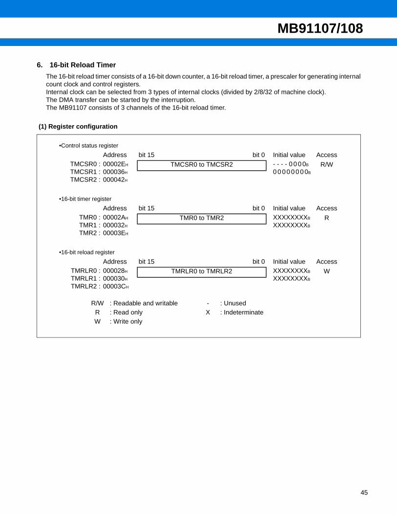
6. 16-bit Reload Timer
The 16-bit reload timer consists of a 16-bit down counter, a 16-bit reload timer, a prescaler for generating internalcount clock and control registers.Internal clock can be selected from 3 types of internal clocks (divided by 2/8/32 of machine clock).The DMA transfer can be started by the interruption.The MB91107 consists of 3 channels of the 16-bit reload timer.
(1) Register configuration
•Control status register
Address bit 15 bit 0 Initial value AccessTMCSR0 :TMCSR1 :TMCSR2 :
00002EH
000036H
000042H
TMCSR0 to TMCSR2 - - - - 0 0 0 0B
0 0 0 0 0 0 0 0B
R/W
•16-bit timer register
Address bit 15 bit 0 Initial value AccessTMR0 :TMR1 :TMR2 :
00002AH
000032H
00003EH
TMR0 to TMR2 XXXXXXXXB
XXXXXXXXB
R
•16-bit reload register
Address bit 15 bit 0 Initial value AccessTMRLR0 :TMRLR1 :TMRLR2 :
000028H
000030H
00003CH
TMRLR0 to TMRLR2 XXXXXXXXB
XXXXXXXXB
W
R/W : Readable and writable - : UnusedR : Read only X : IndeterminateW : Write only
45
MB91107/108
46
(2) Block diagram
RELD
OUTE
OUTL
INTE
UF
CNTE
TRG
OUTCTL.
CSL1
CSL0
MOD2
MOD1
MOD0
16
8
16
2
3
2
IN CTL.
φ 2
φ 2
φ 21 3 5
3
EXCK
GATE2
IRQ
R|BUS
UF
PWM (ch 0, ch 1)A/D (ch 2)
16-bit reload register
Reload
16-bit down counter
Retrigger
Clock selector
Prescaler clear
Internal clock
MB91107/108
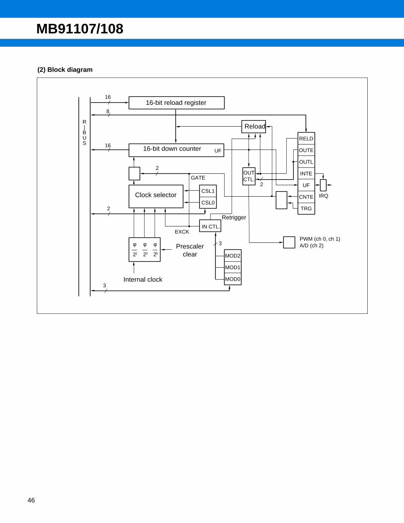
7. Bit Search Module
The bit search module detects transitions of data (0 to 1/1 to 0) on the data written on the input registers andreturns locations of the transitions.
(1) Register configuration
(2) Block diagram
Address bit 31 bit 0 Initial value Access
0003F0H BSD0XXXXXXXXXXXXXXXXB
XXXXXXXXXXXXXXXXBW Zero-detection data register
0003F4H BSD1XXXXXXXXXXXXXXXXB
XXXXXXXXXXXXXXXXBR/W Single-detection data register
0003F8H BSDCXXXXXXXXXXXXXXXXB
XXXXXXXXXXXXXXXXBW Detection data register
0003FCH BSRRXXXXXXXXXXXXXXXXB
XXXXXXXXXXXXXXXXBR Search result register
R/W : Readable and writableR : Read onlyW : Write onlyX : Indeterminate
D-BUS
Addressdecoder
Input latch
Detection mode
Single-detection data register
Bit search circuit
Search result
47
MB91107/108
48
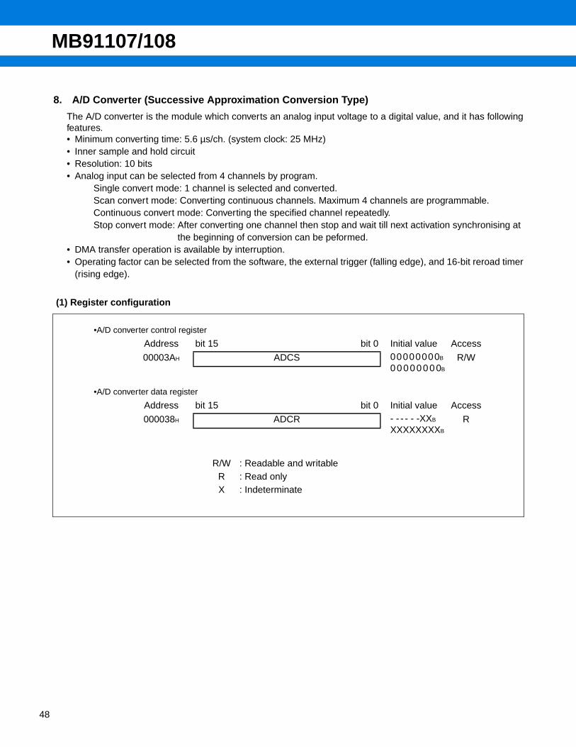
8. A/D Converter (Successive Approximation Conversion Type)
The A/D converter is the module which converts an analog input voltage to a digital value, and it has followingfeatures.• Minimum converting time: 5.6 µs/ch. (system clock: 25 MHz)• Inner sample and hold circuit• Resolution: 10 bits• Analog input can be selected from 4 channels by program.
Single convert mode: 1 channel is selected and converted.Scan convert mode: Converting continuous channels. Maximum 4 channels are programmable.Continuous convert mode: Converting the specified channel repeatedly.Stop convert mode: After converting one channel then stop and wait till next activation synchronising at
the beginning of conversion can be peformed.• DMA transfer operation is available by interruption.• Operating factor can be selected from the software, the external trigger (falling edge), and 16-bit reroad timer
(rising edge).
(1) Register configuration
•A/D converter control register
Address bit 15 bit 0 Initial value Access
00003AH ADCS 0 0 0 0 0 0 0 0B 0 0 0 0 0 0 0 0B
R/W
•A/D converter data register
Address bit 15 bit 0 Initial value Access
000038H ADCR - - - - - -XXB
XXXXXXXXB
R
R/W : Readable and writableR : Read onlyX : Indeterminate
MB91107/108
(2) Block diagram
AVCC
AVRHAVSS
MPX
AN0
AN1
AN2
AN3
ATG
φ
ADCR
ADCS
R|BUS
Internal voltagegenerator
A/D control registerTrigger start
TIM0 (Internal connection) (Reload timer ch2)
(Peripheral clock)
Operating clock
Prescaler
Inpu
t circ
uit
Dec
oder Data register
Successive approxi-mation register
Comparator
Sample & hold circuit
Timer start
49
MB91107/108
50
9. Interrupt Controller
The interrupt controller processes interrupt acknowledgments and arbitration between interrupts.
•Hardware configuration
This module consists of the following components:• ICR register• Interrupt priority evaluation circuit• Interrupt level/interrupt number (vector) generator• HOLD request cancel request generator
•Main Features
The major functions of this module are listed below:• NMI request/interrupt request detection• Priority evaluation (interrupt level and number)• Transfer of interrupt level as evaluation factor (to the CPU)• Transfer of interrupt number as evaluation factor (to the CPU)• Instruction of returning from the stop mode by NMI/interrupt generation• Generating a request to cancel the HOLD request to the bus master
MB91107/108
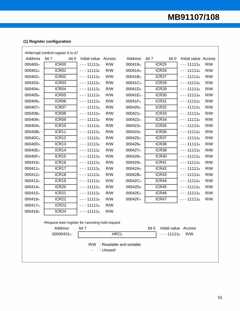
(1) Register configuration
•Interrupt control register 0 to 47
Address bit 7 bit 0 Initial value Access Address bit 7 bit 0 Initial value Access
000400H ICR00 - - - 11111B R/W 000419H ICR25 - - - 11111B R/W
000401H ICR01 - - - 11111B R/W 00041AH ICR26 - - - 11111B R/W
000402H ICR02 - - - 11111B R/W 00041BH ICR27 - - - 11111B R/W
000403H ICR03 - - - 11111B R/W 00041CH ICR28 - - - 11111B R/W
000404H ICR04 - - - 11111B R/W 00041DH ICR29 - - - 11111B R/W
000405H ICR05 - - - 11111B R/W 00041EH ICR30 - - - 11111B R/W
000406H ICR06 - - - 11111B R/W 00041FH ICR31 - - - 11111B R/W
000407H ICR07 - - - 11111B R/W 000420H ICR32 - - - 11111B R/W
000408H ICR08 - - - 11111B R/W 000421H ICR33 - - - 11111B R/W
000409H ICR09 - - - 11111B R/W 000422H ICR34 - - - 11111B R/W
00040AH ICR10 - - - 11111B R/W 000423H ICR35 - - - 11111B R/W
00040BH ICR11 - - - 11111B R/W 000424H ICR36 - - - 11111B R/W
00040CH ICR12 - - - 11111B R/W 000425H ICR37 - - - 11111B R/W
00040DH ICR13 - - - 11111B R/W 000426H ICR38 - - - 11111B R/W
00040EH ICR14 - - - 11111B R/W 000427H ICR39 - - - 11111B R/W
00040FH ICR15 - - - 11111B R/W 000428H ICR40 - - - 11111B R/W
000410H ICR16 - - - 11111B R/W 000429H ICR41 - - - 11111B R/W
000411H ICR17 - - - 11111B R/W 00042AH ICR42 - - - 11111B R/W
000412H ICR18 - - - 11111B R/W 00042BH ICR43 - - - 11111B R/W
000413H ICR19 - - - 11111B R/W 00042CH ICR44 - - - 11111B R/W
000414H ICR20 - - - 11111B R/W 00042DH ICR45 - - - 11111B R/W
000415H ICR21 - - - 11111B R/W 00042EH ICR46 - - - 11111B R/W
000416H ICR22 - - - 11111B R/W 00042FH ICR47 - - - 11111B R/W
000417H ICR23 - - - 11111B R/W
000418H ICR24 - - - 11111B R/W
•Request level register for canceling hold request
Address bit 7 bit 0 Initial value Access
00000431H HRCL - - - 11111B R/W
R/W : Readable and writable- : Unused
51

MB91107/108
52
(2) Block diagram
*1 : DLY I stands for delayed interrupt module (delayed interrupt generation block) (refer to the section “11. Delayed Interrupt Module” for detail).
*2 : INT0 is a wake-up signal to clock control block in the sleep or stop status.
*3 : HLDCAN is a bus release request signal for bus masters other than CPU.
*4 : LEVEL 4 to LEVEL 0 are interrupt level outputs.
*5 : VCT5 to VCT0 are interrupt vector outputs.
INT0∗2
OR
NMI
RI00
RI47
(DLYIRQ) DLYI∗1
4
5
6
LEVEL4 ∼ 0∗4
HLDCAN∗3
VCT5 ∼ 0∗5
R-BUS
IM
ICR00
ICR47
Priority judgment
NMIprocessing
LEVEL judgment
VECTOR judgment
LEVEL, VECTOR
generation
HLDREQcancel request

MB91107/108
10. External Interrupt/NMI Control Block
The external interrupt/NMI control block controls external interrupt request signals input to NMI pin and INT0 toINT7 pins. Detecting levels can be selected from “H”, “L”, rising edge and falling edge (not for NMI pin).
(1) Register configuration
(2) Block diagram
•Interrupt enable register
Address bit 15 bit 8 bit 7 bit 0 Initial value Access
000095H EIRR ENIR 00000000B R/W
•External interrupt cause register
bit 15 bit 8 bit 7 bit 0
000094H EIRR ENIR 00000000B R/W
•Request level setting register
bit 15 bit 8 bit 7 bit 0
000099H EIRR ENIR 00000000B R/W
9 9 INT0 ~ INT7 NMI
8
8
8
R BUS
Interrupt request
Interrupt enable register
Gate Cause F/
Request level setting register
Interrupt cause register
Edge detection circuit
53

MB91107/108
54
11. Delayed Interrupt Module
Delayed interrupt module is a module which generates a interrupt for changing a task. By using this delayedinterrupt module, an interrupt request to CPU can be generated/cancelled by the software.Refer to the section “9. Interrupt Controller” for delayed interrupt module block diagram.
•Register configuration
•Delayed interrupt control register
Address bit 7 bit 0 Initial value Access
000430H DICR - - - - - - - 0B R/W
R/W : Readable and writable- : Unused

MB91107/108
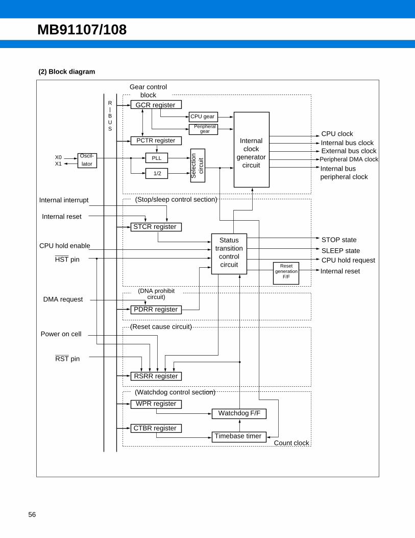
12. Clock Generation (Low-power consumption mechanism)
The clock control block is a module which undertakes the following functions.• CPU clock generation (including gear function)• Peripheral clock generation (including gear function)• Reset generation and cause hold• Standby function (including hardware standby)• DMA request prohibit• PLL (multiplier circuit) embedded
(1) Register configuration
•Reset cause register/watchdog cycle control register
Address bit 15 bit 10 bit 8 bit 0 Initial value Access
000480H RSRR WTCR (STCR) 1XXXX - 0 0B R/W
•Stand-by controled register
Address bit 15 bit 10 bit 8 bit 0 Initial value
000481H (RSRR/WTCR) STCR 0 0 0 111 - - B R/W
•DMA controlerrequest prohibit resister
Address bit 15 bit 8 bit 0 Initial value
000482H PDRR (CTBR) - - - - 0 0 0 0B R/W
•Timebase timer clear resister
Address bit 15 bit 8 bit 0 Initial value
000483H PDRR (CTBR) XXXXXXXXB W
•Gear control resister
Address bit 15 bit 8 bit 0 Initial value
000484H GCR (WPR) - - - - 0 0 0 0B R/W
•Watchdog reset generation postpone resister
Address bit 15 bit 8 bit 0 Initial value
000485H (GCR) WPR XXXXXXXXB W
•PLL control resister
Address bit 15 bit 8 bit 0 Initial value
000488H PCTR Vacancy 0 0 - - 0 - - - B W
R/W : Readable and writableW : Write only- : UnusedX : Indeterminate
55
MB91107/108
56
(2) Block diagram
X0X1
PLL
1/2
R|BUS
Internal reset
CPU hold enable
DMA request
Power on cell
RST pin
GCR register
CPU gear
Statustransitioncontrolcircuit
PDRR register
(Watchdog control section)
Timebase timer
CPU clockInternal bus clockExternal bus clock
Internal bus peripheral clock
STOP state
SLEEP stateCPU hold requestHST pin
Gear control block
Peripheralgear
Peripheral DMA clock
PCTR register
STCR register
Count clock
Watchdog F/F
(Reset cause circuit)
(DNA prohibitcircuit)
RSRR register
WPR register
CTBR register
Internal interrupt
Oscil-
lator
Sel
ectio
n ci
rcui
t(Stop/sleep control section)
Resetgeneration
F/F
Internal clock
generator circuit
Internal reset

MB91107/108
13. External Bus Interface
The external bus interface controls the interface between the device and the external memory and also theexternal I/O, and has the following features.• 25-bit (32 Mbytes) address output• 6 independent banks owing to the chip select function.
Can be set to anywhere on the logical address space for minimum unit 64 Kbytes.Total 32 Mbytes × 6 area setting is available by the address pin and the chip select pin.
• 8/16-bit bus width setting are available for every chip select area.Areas 6 and 7 allow the inclusive areas to be set.
• Programmable automatic memory wait (max. for 7 cycles) can be inserted.• DRAM interface support• Three kinds of DRAM interface: Double CAS DRAM (normally DRAM I/F)
Single CAS DRAMHyper DRAM
• 2 banks independent control (RAS, CAS, etc. control signals)• DRAM select is available from 2CAS/1WE and 1CAS/2WE.• Hi-speed page mode supported• CBR/self refresh supported• Programmable wave form• Unused address/data pin can be used for I/O port.• Little endian mode supported• Clock doubler: Internal bus 50 MHz, external bus 25 MHz
(1) Register configuration
(Continued)
•Area selection resister 1 to 5
Address bit 15 bit 0 Initial value Access00060CH ASR1 0 0 0 0 0 0 0 0B 0 0 0 0 0 0 0 1B W000610H ASR2 0 0 0 0 0 0 0 0B 0 0 0 0 0 0 1 0B W000614H ASR3 0 0 0 0 0 0 0 0B 0 0 0 0 0 0 1 1B W000618H ASR4 0 0 0 0 0 0 0 0B 0 0 0 0 0 1 0 0B W00061CH ASR5 0 0 0 0 0 0 0 0B 0 0 0 0 0 1 0 1B W
•Area mask resister 1 to 5
Address bit 15 bit 0 Initial value00060EH AMR1 0 0 0 0 0 0 0 0B 0 0 0 0 0 0 0 0B W000612H AMR2 0 0 0 0 0 0 0 0B 0 0 0 0 0 0 0 0B W000616H AMR3 0 0 0 0 0 0 0 0B 0 0 0 0 0 0 0 0B W00061AH AMR4 0 0 0 0 0 0 0 0B 0 0 0 0 0 0 0 0B W00061EH AMR5 0 0 0 0 0 0 0 0B 0 0 0 0 0 0 0 0B W
57
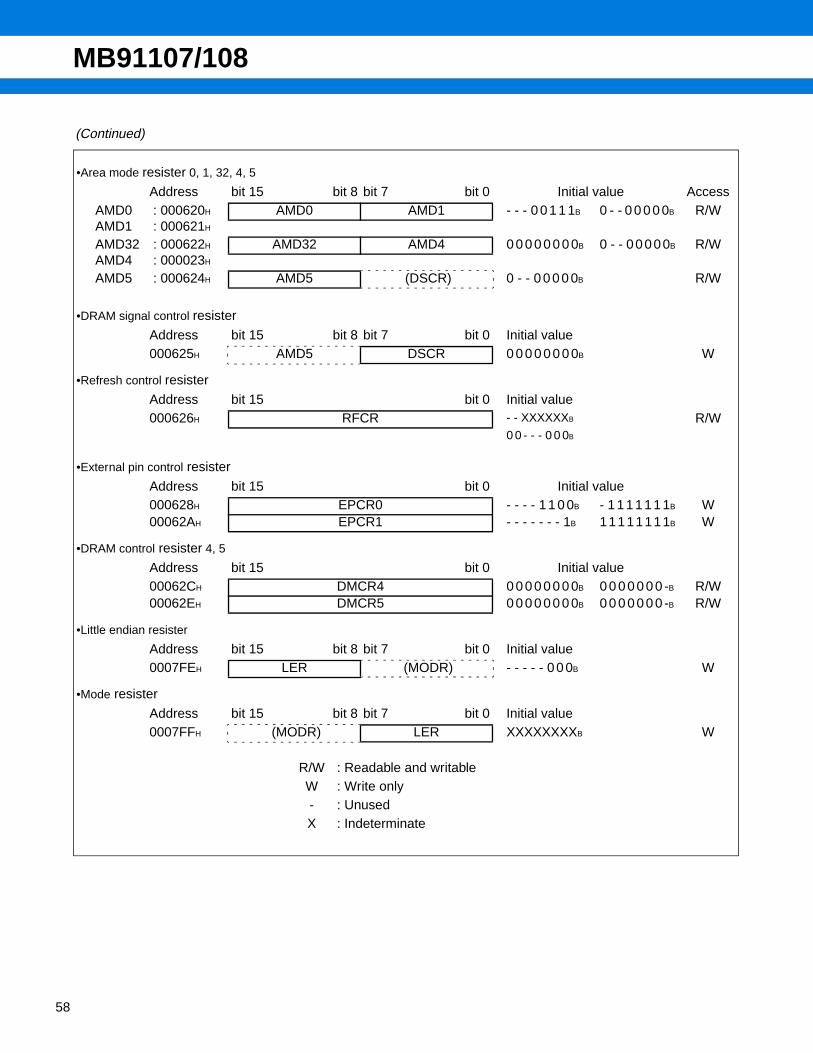
MB91107/108
58
(Continued)
•Area mode resister 0, 1, 32, 4, 5
Address bit 15 bit 8 bit 7 bit 0 Initial value AccessAMD0AMD1
: 000620H
: 000621H
AMD0 AMD1 - - - 0 0 1 1 1B 0 - - 0 0 0 0 0B R/W
AMD32AMD4
: 000622H
: 000023H
AMD32 AMD4 0 0 0 0 0 0 0 0B 0 - - 0 0 0 0 0B R/W
AMD5 : 000624H AMD5 (DSCR) 0 - - 0 0 0 0 0B R/W
•DRAM signal control resister
Address bit 15 bit 8 bit 7 bit 0 Initial value000625H AMD5 DSCR 0 0 0 0 0 0 0 0B W
•Refresh control resister
Address bit 15 bit 0 Initial value000626H RFCR - - XXXXXXB R/W
0 0 - - - 0 0 0B
•External pin control resister
Address bit 15 bit 0 Initial value000628H EPCR0 - - - - 1 1 0 0B - 1 1 1 1 1 1 1B W00062AH EPCR1 - - - - - - - 1B 1 1 1 1 1 1 1 1B W
•DRAM control resister 4, 5
Address bit 15 bit 0 Initial value00062CH DMCR4 0 0 0 0 0 0 0 0B 0 0 0 0 0 0 0 -B R/W00062EH DMCR5 0 0 0 0 0 0 0 0B 0 0 0 0 0 0 0 -B R/W
•Little endian resister
Address bit 15 bit 8 bit 7 bit 0 Initial value0007FEH LER (MODR) - - - - - 0 0 0B W
•Mode resister
Address bit 15 bit 8 bit 7 bit 0 Initial value0007FFH (MODR) LER XXXXXXXXB W
R/W : Readable and writableW : Write only- : UnusedX : Indeterminate
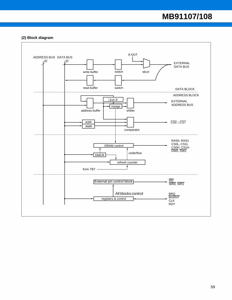
MB91107/108
(2) Block diagram
A-OUT
MUX
inpage
CS0 ∼ CS7
RAS0, RAS1CS0L, CS1LCS0H, CS1HDW0, DW1
RDWR0, WR1
BRQBGRNTCLKRDY
3232ADDRESS BUS DATA BUS
write buffer
read buffer
switch
switch
EXTERNALDATA BUS
+1or+2
address buffer
ASRAMR
shifter
comparator
DATA BLOCK
ADDRESS BLOCK
EXTERNALADDRESS BUS
DRAM control
underflowDMCR
from TBT
refresh counter
registers & control
All blocks control
External pin control block
59

MB91107/108
60
ELECTRICAL CHARACTERISTICS1. Absolute Maximum Ratings
(AVSS = VSS = 0.0 V)
*1 : VCC must not be less than VSS – 0.3 V.
*2 : Care must be taken that AVCC and AVRH do not exceed VCC + 0.3 V, such as when turning on the device.Also, care must be taken that AVRH does not exceed AVCC.
*3 : Maximum output current is a peak current value measured at a corresponding pin.
*4 : Average output current is an average current for a 100 ms period at a corresponding pin.
*5 : Average total output current is an average current for a 100 ms period for all corresponding pins.
WARNING: Semiconductor devices can be permanently damaged by application of stress (voltage, current, temperature, etc.) in excess of absolute maximum ratings. Do not exceed these ratings.
Parameter SymbolValue
Unit RemarksMin. Max.
Power supply voltage VCC VSS − 0.3 VSS + 4.0 V *1
Analog supply voltage AVCC VSS − 0.3 VSS + 4.0 V *2
Analog reference voltage AVRH VSS − 0.3 VSS + 4.0 V *2
Input voltage VI VSS − 0.3 VCC + 0.3 V
Analog pin input voltage VIA VSS − 0.3 AVCC + 0.3 V
Output voltage VO VSS − 0.3 VCC + 0.3 V
“L” level maximum output current IOL 10 mA *3
“L” level average output current IOLAV 8 mA *4
“L” level total maximum output current ΣIOL 100 mA
“L” level total average output current ΣIOLAV 50 mA *5
“H” level maximum output current IOH −10 mA *3
“H” level average output current IOHAV −4 mA *4
“H” level total maximum output current ΣIOH −50 mA
“H” level total average output current ΣIOHAV −20 mA *5
Power consumption PD 500 mW
Operating temperature TA 0 +70 °C
Storage temperature Tstg −55 +150 °C

MB91107/108
2. Recommended Operating Conditions (AVSS = VSS = 0.0 V)
WARNING: The recommended operating conditions are required in order to ensure the normal operation of thesemiconductor device. All of the device’s electrical characteristics are warranted when the device isoperated within these ranges.
Always use semiconductor devices within their recommended operating condition ranges. Operationoutside these ranges may adversely affect reliability and could result in device failure.No warranty is made with respect to uses, operating conditions, or combinations not represented onthe data sheet. Users considering application outside the listed conditions are advised to contact theirFUJITSU representatives beforehand.
Parameter SymbolValue
Unit RemarksMin. Max.
Power supply voltage
VCC 3.0 3.6
V
Normal operation
VCC 3.0 3.6Retaining the RAM state in stop mode
Analog supply voltage AVCC VSS − 0.3 VSS + 3.6 V
Analog reference voltage AVRH AVSS AVCC V
Operating temperature TA 0 +70 °C
61
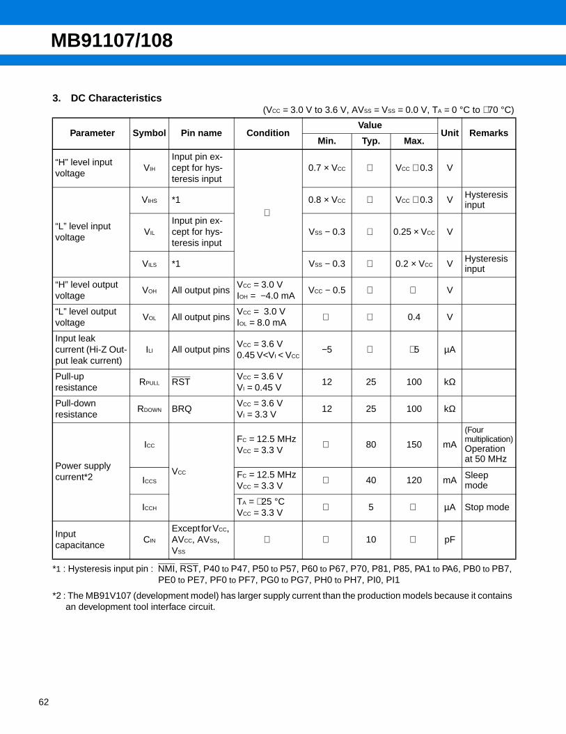
MB91107/108
62
3. DC Characteristics (VCC = 3.0 V to 3.6 V, AVSS = VSS = 0.0 V, TA = 0 °C to +70 °C)
*1 : Hysteresis input pin : NMI, RST, P40 to P47, P50 to P57, P60 to P67, P70, P81, P85, PA1 to PA6, PB0 to PB7, PE0 to PE7, PF0 to PF7, PG0 to PG7, PH0 to PH7, PI0, PI1
*2 : The MB91V107 (development model) has larger supply current than the production models because it contains an development tool interface circuit.
Parameter Symbol Pin name ConditionValue
Unit RemarksMin. Typ. Max.
“H” level input voltage
VIH
Input pin ex-cept for hys-teresis input
0.7 × VCC VCC + 0.3 V
“L” level input voltage
VIHS *1 0.8 × VCC VCC + 0.3 V Hysteresis input
VIL
Input pin ex-cept for hys-teresis input
VSS − 0.3 0.25 × VCC V
VILS *1 VSS − 0.3 0.2 × VCC V Hysteresis input
“H” level output voltage
VOH All output pinsVCC = 3.0 VIOH = −4.0 mA
VCC − 0.5 V
“L” level output voltage
VOL All output pinsVCC = 3.0 VIOL = 8.0 mA
0.4 V
Input leakcurrent (Hi-Z Out-put leak current)
ILI All output pinsVCC = 3.6 V0.45 V<VI < VCC
−5 +5 µA
Pull-upresistance
RPULL RSTVCC = 3.6 VVI = 0.45 V
12 25 100 kΩ
Pull-downresistance
RDOWN BRQVCC = 3.6 VVI = 3.3 V
12 25 100 kΩ
Power supply current*2
ICC
VCC
FC = 12.5 MHzVCC = 3.3 V
80 150 mA
(Four multiplication)Operation at 50 MHz
ICCSFC = 12.5 MHzVCC = 3.3 V
40 120 mA Sleep mode
ICCHTA = +25 °CVCC = 3.3 V
5 µA Stop mode
Input capacitance
CIN
Except for VCC, AVCC, AVSS, VSS
10 pF

MB91107/108
4. AC Characteristics•Measurement Conditions
The following conditions applies to measurement items unless otherwise specified.
VOH
VOL
VIH
VIL
VCC
0 V
Input Output
VCC = 3.0 V to 3.6 V
Note: The rise/fall time of input is 10 ns or less.
VIH 1 / 2 × VCC VOH 1 / 2 × VCC
VIL 1 / 2 × VCC VOL 1 / 2 × VCC
•AC characteristics measurement conditions
C = 50 pF
Output pin
•Load conditions
63

MB91107/108
64
(1) Clock Timings (VCC = 3.0 V to 3.6 V, AVSS = VSS = 0.0 V, TA = 0 °C to +70 °C)
*1 : Frequency shift ratio stands for deviation ratio of the operating clock from the center frequency in the clock multiplication system.
*2 : These values are for a minimum clock of 10 MHz input to X0, a divide-by-2 system of the source oscillation and a 1/8 gear.
Parameter Sym-bol
Pin name Condition
ValueUnit Remarks
Min. Max.
Clock frequency (1) FCX0X1
12.5 12.5 MHz
Self-oscillation 12.5 MHzInternal operation at 50 MHz (Using PLL, 4 multiplication)
Clock cycle time tCX0X1
80 ns
Frequency shift ratio ∗1 (when locked) ∆f 5 %
Clock frequency (2) FCX0X1
10 25 MHzSelf-oscillation(divide-by-2 input)
Clock frequency (3) FCX0X1
10 25 MHzExternal clock(divide-by-2 input)
Clock cycle time tCX0X1
40 100 ns
Input clock pulse width
PWH
PWL
X0X1
12.5 to 25 MHz
20 ns Input to X0, X1
PWH X0Less than 12.5 MH
25 ns Input to X0 only
Input clock rising/falling time
tCR
tCF
X0X1
8 ns (tCR + tCF)
Internal operating clock frequency
fCP
0.625 × 2 50 MHz CPU system
fCPP 0.625 × 2 25 MHz Peripheral system
Internal operating clock cycle time
tCP 20 1600*2 ns CPU system
tCPP 40 1600*2 ns Peripheral system
∆f = × 100 (%)αf0
f0
+α
−α
+
−
Center frequency

MB91107/108
0 5025 (MHz)
50
12.5
00
25fC(MHz)
0.625
3.6
3.0
(V)
fCP / fCPP (MHz)
5
fCP
fCP / fCPP
VCC
25
10
fCPP
CPU
0.8 VCC
0.2 VCC
tCF tCR
tC
PWH PWL
• Clock timing rating measurement conditions
• Operation warranty range
• External / internal clock setting range
Pow
er s
uppl
y
Internal clock
Normal operation warranty range (TA = 0 °C to +70 °C).Net masked area are fCPP.
Max
. int
erna
l clo
ck fr
eque
ncy
setti
ng
LL system (12.5 MHz / 4 multiplication)
Peripheral
divide-by-2 system
External clockSelf-oscillation
Note: •When using PLL, the external clock must be used need 12.5 MHz.•PLL oscillation stabilizing period > 100 µs•The setting of internal clock must be within above ranges.
General oscillation input clock
65

MB91107/108
66
(2) Clock Output Timing (VCC = 3.0 V to 3.6 V, AVSS = VSS = 0.0 V, TA = 0 °C to +70 °C)
*1 : tCYC is a frequency for 1 clock cycle including a gear cycle.
*2 : Rating at a gear cycle of × 1.When a gear cycle of 1/2, 1/4, 1/8 is selected, substitute “n” in the following equations with 1/2, 1/4, 1/8, respectively.
Min. : (1 – n/2) × tCYC – 10Max. : (1 – n/2) × tCYC + 10Select a gear cycle of × 1 when using the doubler.
*3 : Rating at a gear cycle of × 1.When a gear cycle of 1/2, 1/4, 1/8 is selected, substitute “n” in the following equations with 1/2, 1/4, 1/8,
respectively.Min.: n/2 × tCYC – 10Max.: n/2 × tCYC + 10
Select a gear cycle of × 1 when using the doubler.
Parameter Symbol Pin name
Condi-tion
ValueUnit Remarks
Min. Max.
Cycle time tCYC CLK
tCP ns
*1
2 × tCP Using the doubler
CLK↑→CLK↓ tCHCL CLK 1 / 2 × tCYC − 10 1 / 2 × tCYC + 10 ns *2
CLK↓→CLK↑ tCLCH CLK 1 / 2 × tCYC − 10 1 / 2 × tCYC + 10 ns *3
CLKVOH
VOL
VOH
tCYC
tCLCHtCHCL

MB91107/108
The relation between source oscillation input and CLK pin for configured by CHC/CCK1/CCK0 settings of GCR(gear control register) is as follows. However, in this chart source oscillation input means X0 input clock.
tCYC
tCYC
tCYC
tCYC
tCYC
tCYC
Source oscillation input (When using the dou-blure)
• PLL system (CHC bit of GCR setto “0”) (a) Gear × 1 CLK pin
CCK1/0 : “00”
Source oscillation input
• 2 dividing system (CHC bit of GCR setto “1”)
(a) Gear × 1 CLK pinCCK1/0 : “00”
(b) Gear × 1/2 CLK pinCCK1/0 : “01”
(c) Gear × 1/4 CLK pinCCK1/0 : “10”
(d) Gear × 1/8 CLK pinCCK1/0 : “11”
67
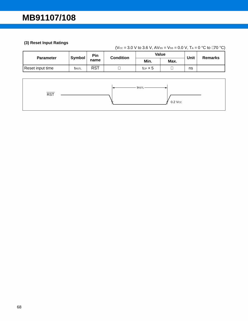
MB91107/108
68
(3) Reset Input Ratings (VCC = 3.0 V to 3.6 V, AVSS = VSS = 0.0 V, TA = 0 °C to +70 °C)
Parameter Symbol Pin name Condition
ValueUnit Remarks
Min. Max.
Reset input time tRSTL RST tCP × 5 ns
RST
0.2 VCC
tRSTL

MB91107/108
(4) Power-on Reset (VCC = 3.0 V to 3.6 V, AVSS = VSS = 0.0 V, TA = 0 °C to +70 °C)
Parameter Symbol Pin name Condition
ValueUnit Remarks
Min. Max.
Power supply rising time
tR VCC VCC = 3.3 V 18 msVCC < 0.2 Vbefore the power supply rising
Power supply shut off time
tOFF VCC 1 msRepeatedoperations
0.2 V
tR
0.9 VCC
VCC
VSS
VCC
RST
VCC
tOFF
tRSTL
•Notes1) Sudden change in supply voltage during operation may initiate a power-on sequence. To change supply volt-
age during operation, it is recommended to smoothly raise the voltage to avoid rapid fluctuations in the supply voltage.
A voltage rising rate of 50 mV/ms or less is recommended.
2) Set RST pin to “L” level when turning on the device, at least the tRSTL duration after the supply voltage reaches VCC is necessary before turning the RST to “H” level.
Not less than 3 V
3) If the supply voltage goes below the lower limit of the guaranteed operating voltage range, be sure to restart the power supply from the VSS level. This is because an internal power-on reset must be generated to restart operation without allowing the internal circuit to run out of control.The guaranteed operating voltage range of MB91107 is from 3.0 to 3.6 V.
69
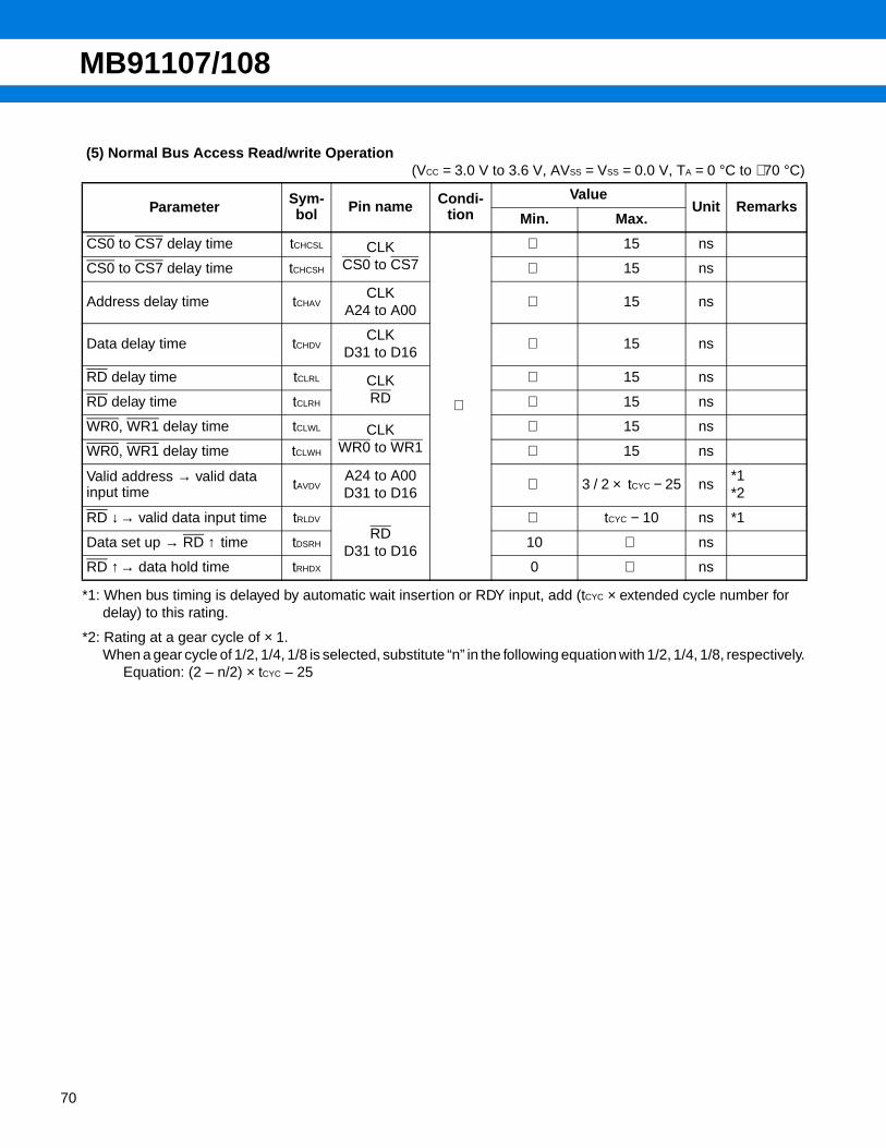
MB91107/108
70
(5) Normal Bus Access Read/write Operation (VCC = 3.0 V to 3.6 V, AVSS = VSS = 0.0 V, TA = 0 °C to +70 °C)
*1: When bus timing is delayed by automatic wait insertion or RDY input, add (tCYC × extended cycle number for delay) to this rating.
*2: Rating at a gear cycle of × 1.When a gear cycle of 1/2, 1/4, 1/8 is selected, substitute “n” in the following equation with 1/2, 1/4, 1/8, respectively.
Equation: (2 – n/2) × tCYC – 25
Parameter Sym-bol Pin name Condi-
tionValue
Unit RemarksMin. Max.
CS0 to CS7 delay time tCHCSL CLKCS0 to CS7
15 ns
CS0 to CS7 delay time tCHCSH 15 ns
Address delay time tCHAVCLK
A24 to A00 15 ns
Data delay time tCHDVCLK
D31 to D16 15 ns
RD delay time tCLRL CLKRD
15 ns
RD delay time tCLRH 15 ns
WR0, WR1 delay time tCLWL CLKWR0 to WR1
15 ns
WR0, WR1 delay time tCLWH 15 ns
Valid address → valid data input time tAVDV
A24 to A00D31 to D16
3 / 2 × tCYC − 25 ns*1*2
RD ↓→ valid data input time tRLDV
RDD31 to D16
tCYC − 10 ns *1
Data set up → RD ↑ time tDSRH 10 ns
RD ↑→ data hold time tRHDX 0 ns

MB91107/108
2.4 VCLK 0.8 V2.4 V
0.8 V
BA2
2.4 V
0.8 V
2.4 V0.8 V
tCLRL
0.8 V
tCLWL
0.8 V
tCHDV
0.8 V2.4 V
0.8 V2.4 V
tCLRH
2.4 V
2.4 V0.8 V
2.4 V0.8 V
tDSRH
tRHDX
tCLWH
2.4 V
2.4 V0.8 V
tCHCSH
2.4 VCS0 ∼ CS7
A24 ∼ A00
RD
D31 ∼ D16
WR0 ∼ WR1
D31 ∼ D16
BA1
tCYC
tCHCSL
tRLDV
tAVDV
tCHAV
Read
Write
71
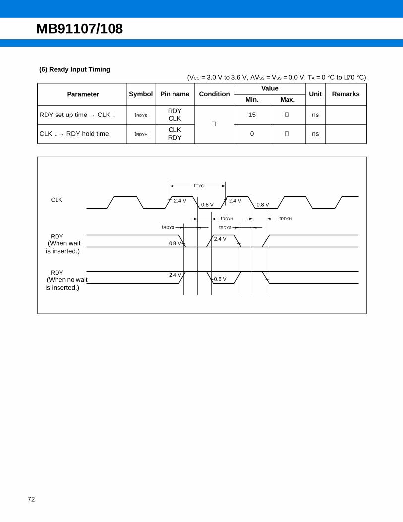
MB91107/108
72
(6) Ready Input Timing (VCC = 3.0 V to 3.6 V, AVSS = VSS = 0.0 V, TA = 0 °C to +70 °C)
Parameter Symbol Pin name ConditionValue
Unit RemarksMin. Max.
RDY set up time → CLK ↓ tRDYSRDYCLK
15 ns
CLK ↓→ RDY hold time tRDYHCLKRDY
0 ns
CLK 2.4 V 2.4 V0.8 V 0.8 V
0.8 V2.4 V
2.4 V0.8 V
tRDYH tRDYH
RDY
RDY
tCYC
tRDYStRDYS
(When waitis inserted.)
(When no wait is inserted.)
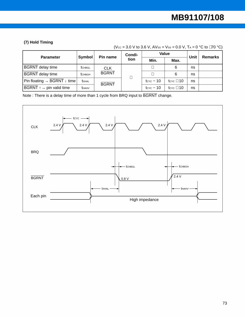
MB91107/108
(7) Hold Timing (VCC = 3.0 V to 3.6 V, AVSS = VSS = 0.0 V, TA = 0 °C to +70 °C)
Note : There is a delay time of more than 1 cycle from BRQ input to BGRNT change.
Parameter Symbol Pin name Condi-tion
ValueUnit Remarks
Min. Max.
BGRNT delay time tCHBGL CLKBGRNT
6 ns
BGRNT delay time tCHBGH 6 ns
Pin floating → BGRNT ↓ time tXHALBGRNT
tCYC − 10 tCYC + 10 ns
BGRNT ↑→ pin valid time tHAHV tCYC − 10 tCYC + 10 ns
CLK 2.4 V
tCHBGL
0.8 V
2.4 V 2.4 V 2.4 V
2.4 V
tCHBGH
BRQ
BGRNT
tCYC
tHAHVtXHAL
Each pinHigh impedance
73
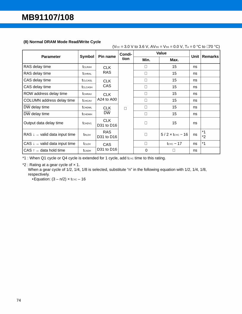
MB91107/108
74
(8) Normal DRAM Mode Read/Write Cycle (VCC = 3.0 V to 3.6 V, AVSS = VSS = 0.0 V, TA = 0 °C to +70 °C)
*1 : When Q1 cycle or Q4 cycle is extended for 1 cycle, add tCYC time to this rating.
*2 : Rating at a gear cycle of × 1.When a gear cycle of 1/2, 1/4, 1/8 is selected, substitute “n” in the following equation with 1/2, 1/4, 1/8, respectively.
•Equation: (3 – n/2) × tCYC – 16
Parameter Symbol Pin name Condi-tion
ValueUnit Remarks
Min. Max.
RAS delay time tCLRAH CLKRAS
15 ns
RAS delay time tCHRAL 15 ns
CAS delay time tCLCASL CLKCAS
15 ns
CAS delay time tCLCASH 15 ns
ROW address delay time tCHRAV CLKA24 to A00
15 ns
COLUMN address delay time tCHCAV 15 ns
DW delay time tCHDWL CLKDW
15 ns
DW delay time tCHDWH 15 ns
Output data delay time tCHDV1CLK
D31 to D16 15 ns
RAS ↓→ valid data input time tRLDVRAS
D31 to D16 5 / 2 × tCYC − 16 ns
*1*2
CAS ↓→ valid data input time tCLDV CASD31 to D16
tCYC − 17 ns *1
CAS ↑→ data hold time tCADH 0 ns

MB91107/108
0.8 V2.4 V
0.8 V2.4 VD31 to D16
0.8 V2.4 V
0.8 V2.4 V
0.8 V2.4 V
2.4 VCLK 0.8 V
Q2Q1 Q3 Q4 Q5
2.4 V
2.4 V0.8 V
0.8 V 0.8 V2.4 V
tCHRAL
0.8 V
tCLCASL
2.4 V
tCHRAV
0.8 V2.4 V
0.8 V2.4 V
tCADH
0.8 V2.4 V
tCHDWL tCHDWH
tCHDV1
D31 to D16
RAS
CAS
A24 to A00
DW
tCYC
tCLRAH
tCHCAV
tCLCASH
tRLDV
tCLDV
0.8 V2.4 VROW address COLUMN address
Read
Write
75
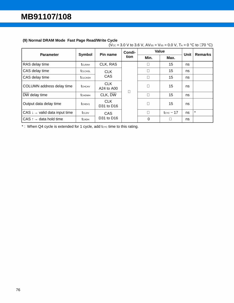
MB91107/108
76
(9) Normal DRAM Mode Fast Page Read/Write Cycle (VCC = 3.0 V to 3.6 V, AVSS = VSS = 0.0 V, TA = 0 °C to +70 °C)
* : When Q4 cycle is extended for 1 cycle, add tCYC time to this rating.
Parameter Symbol Pin name Condi-tion
ValueUnit Remarks
Min. Max.
RAS delay time tCLRAH CLK, RAS
15 ns
CAS delay time tCLCASL CLKCAS
15 ns
CAS delay time tCLCASH 15 ns
COLUMN address delay time tCHCAVCLK
A24 to A00 15 ns
DW delay time tCHDWH CLK, DW 15 ns
Output data delay time tCHDV1CLK
D31 to D16 15 ns
CAS ↓→ valid data input time tCLDV CASD31 to D16
tCYC − 17 ns *
CAS ↑→ data hold time tCADH 0 ns

MB91107/108
0.8 V2.4 V
0.8 V2.4 V
tCLCASH
0.8 V2.4 V
2.4 V
0.8 V2.4 V
0.8 V2.4 V
tCHDWH
tCHDV1
0.8 V2.4 V
D31 to D16
CLK
D31 to D16
RAS
CAS
A24 to A00
DW
Q4 Q5
2.4 V0.8 V
Q5
0.8 V
Q4 Q5
2.4 V0.8 V
tCLRAH
2.4 V
2.4 V0.8 V
tCLCASL
0.8 V2.4 V
tCADH
tCHCAV
tCLDV
COLUMN address COLUMN address COLUMN address
Read Read Read
WriteWrite
77
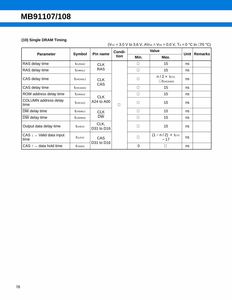
MB91107/108
78
(10) Single DRAM Timing (VCC = 3.0 V to 3.6 V, AVSS = VSS = 0.0 V, TA = 0 °C to +70 °C)
Parameter Symbol Pin name Condi-tion
ValueUnit Remarks
Min. Max.
RAS delay time tCLRAH2 CLKRAS
15 ns
RAS delay time tCHRAL2 15 ns
CAS delay time tCHCASL2 CLKCAS
n / 2 × tCYC
+ tCHCASH2ns
CAS delay time tCHCASH2 15 ns
ROW address delay time tCHRAV2CLK
A24 to A00
15 ns
COLUMN address delay time tCHCAV2 15 ns
DW delay time tCHDWL2 CLKDW
15 ns
DW delay time tCHDWH2 15 ns
Output data delay time tCHDV2CLK,
D31 to D16 15 ns
CAS ↓→ Valid data input time tCLDV2 CAS
D31 to D16
(1 − n / 2) × tCYC − 17
ns
CAS ↑→ data hold time tCADH2 0 ns

MB91107/108
COLUMN-2
tCHCASH2
tCHRAL2
tCHDWH2tCHDWL2
tCHDV2 tCHDV2
D31 to D16
CLK
D31 to D16
RAS
CAS
A24 to A00
DW
Q2 Q3
2.4 V
2.4 V
2.4 V
2.4 V2.4 V 2.4 V 2.4 V0.8 V
0.8 V
0.8 V
2.4 V0.8 V
2.4 V0.8 V
2.4 V0.8 V
2.4 V0.8 V
2.4 V
0.8 V
2.4 V
0.8 V
Q1 Q4S Q4S Q4S
tCADH2
tCLDV2
tCHRAV2 tCHCAV2
tCHCASL2
tCYC
2.4 V 2.4 V
tCLRAH2
2.4 V2.4 V
0.8 V0.8 V
0.8 V
2.4 V0.8 V
2.4 V0.8 V
COLUMN-0 COLUMN-1
∗2
∗1
(Read)
(Read)
(Write)
ROW address
Read-0 Read-1 Read-2
Write-0 Write-1 Write-2
*1 : Q4S indicates Q4SR (Read) of Single DRAM cycle or Q4SW (Write) cycle.
*2 : indicates the timing when the bus cycle begins from the high speed page mode.
79
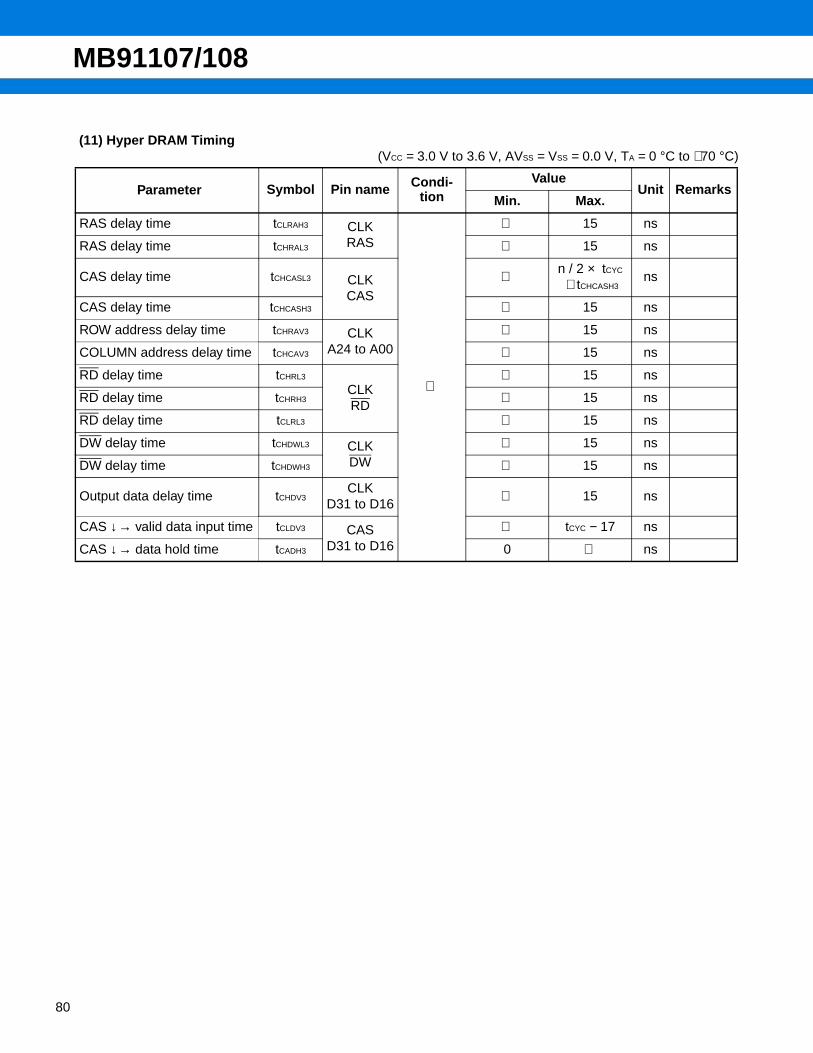
MB91107/108
80
(11) Hyper DRAM Timing (VCC = 3.0 V to 3.6 V, AVSS = VSS = 0.0 V, TA = 0 °C to +70 °C)
Parameter Symbol Pin name Condi-tion
ValueUnit Remarks
Min. Max.
RAS delay time tCLRAH3 CLKRAS
15 ns
RAS delay time tCHRAL3 15 ns
CAS delay time tCHCASL3 CLKCAS
n / 2 × tCYC
+ tCHCASH3ns
CAS delay time tCHCASH3 15 ns
ROW address delay time tCHRAV3 CLKA24 to A00
15 ns
COLUMN address delay time tCHCAV3 15 ns
RD delay time tCHRL3
CLKRD
15 ns
RD delay time tCHRH3 15 ns
RD delay time tCLRL3 15 ns
DW delay time tCHDWL3 CLKDW
15 ns
DW delay time tCHDWH3 15 ns
Output data delay time tCHDV3CLK
D31 to D16 15 ns
CAS ↓→ valid data input time tCLDV3 CASD31 to D16
tCYC − 17 ns
CAS ↓→ data hold time tCADH3 0 ns
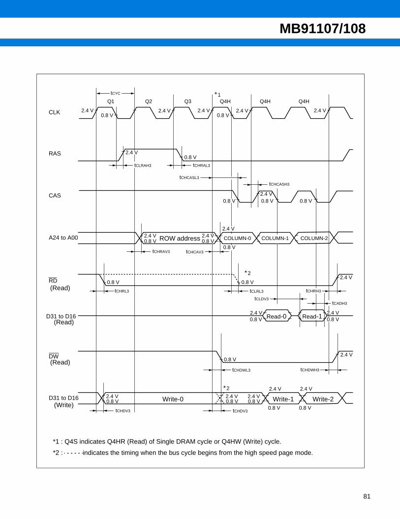
MB91107/108
tCHCASH3
tCHRAL3
tCHDWH3tCHDWL3
tCHDV3 tCHDV3
D31 to D16
CLK
D31 to D16
RAS
CAS
RD
A24 to A00
DW
Q2 Q3
2.4 V
2.4 V
2.4 V
2.4 V2.4 V 2.4 V 2.4 V0.8 V
0.8 V
0.8 V
0.8 V
2.4 V0.8 V
2.4 V0.8 V
2.4 V0.8 V
2.4 V0.8 V
2.4 V
0.8 V
2.4 V
0.8 V
Q1 Q4H Q4H Q4H
0.8 V
tCADH3tCLDV3
tCHRAV3
tCLRL3
0.8 V
tCHRL3
tCHCASL3
tCYC
2.4 V
tCLRAH3
2.4 V2.4 V
0.8 V0.8 V
0.8 V
2.4 V2.4 V0.8 V
COLUMN-0 COLUMN-1
∗2
∗2
∗1
COLUMN-2
tCHRH3
tCHCAV3
0.8 V
2.4 V
0.8 V 0.8 V
(Read)
(Read)
(Read)
(Write)
ROW address
Read-0 Read-1
Write-0 Write-1 Write-2
*1 : Q4S indicates Q4HR (Read) of Single DRAM cycle or Q4HW (Write) cycle.
*2 : indicates the timing when the bus cycle begins from the high speed page mode.
81

MB91107/108
82
(12) CBR Refresh (VCC = 3.0 V to 3.6 V, AVSS = VSS = 0.0 V, TA = 0 °C to +70 °C)
Parameter Symbol Pin name Condi-tion
ValueUnit Remarks
Min. Max.
RAS delay time tCLRAH CLKRAS
15 ns
RAS delay time tCHRAL 15 ns
CAS delay time tCLCASL CLKCAS
15 ns
CAS delay time tCLCASH 15 ns
tCLCASH
CLK
RAS
CAS
0.8 V 0.8 V
R4
2.4 V0.8 V
tCLRAH
R3R2R1
0.8 V
2.4 V 2.4 V
2.4 V0.8 V
tCHRAL
tCLCASL
DW
tCYC
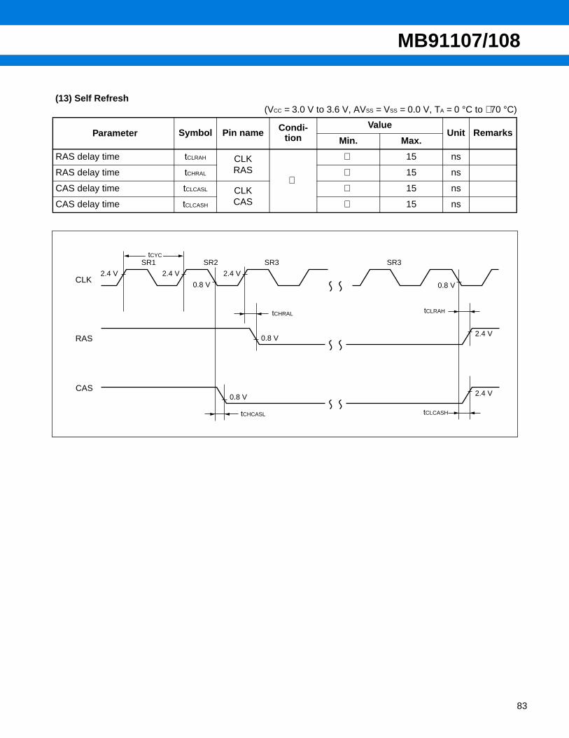
MB91107/108
(13) Self Refresh (VCC = 3.0 V to 3.6 V, AVSS = VSS = 0.0 V, TA = 0 °C to +70 °C)
Parameter Symbol Pin name Condi-tion
ValueUnit Remarks
Min. Max.
RAS delay time tCLRAH CLKRAS
15 ns
RAS delay time tCHRAL 15 ns
CAS delay time tCLCASL CLKCAS
15 ns
CAS delay time tCLCASH 15 ns
CLK
RAS
CAS
0.8 V
tCHRAL
SR1
2.4 V
tCHCASL
tCLRAH
2.4 V
SR2
2.4 V
SR3
0.8 V
0.8 V
SR3
0.8 V
2.4 V
2.4 V
tCLCASH
tCYC
83

MB91107/108
84
(14) UART Timing (VCC = 3.0 V to 3.6 V, AVSS = VSS = 0.0 V, TA = 0 °C to +70 °C)
Notes: • This rating is for AC characteristics in CLK synchronous mode.• tCYCP: A cycle time of peripheral system clock
Parameter Symbol Pin name ConditionValue
Unit RemarksMin. Max.
Serial clock cycle time tSCYC
Internal shift clock mode
8 tCYCP ns
SCLK ↓→ SOUT delay time tSLOV −80 80 ns
Valid SIN → SCLK ↑ tIVSH 100 ns
SCLK ↑→ valid SIN hold time tSHIX 60 ns
Serial clock “H” pulse width tSHSL
External shift clock mode
4 tCYCP ns
Serial clock “L” pulse width tSLSH 4 tCYCP ns
SCLK ↓→ SOUT delay time tSLOV 150 ns
Valid SIN → SCLK ↑ tIVSH 60 ns
SCLK ↑→ valid SIN hold time tSHIX 60 ns

MB91107/108
SCLK
SOUT
SIN
SCLK
SOUT
SIN
tSCYC
tSLOV
tIVSH tSHIX
tSLOV
tSLSH tSHSL
tIVSH tSHIX
2.4 V
0.8 V
2.4 V
0.8 V
2.4 V
0.8 V
0.8 VCC
0.8 VCC
0.2 VCC
0.2 VCC
0.2 VCC
0.8 VCC
• Internal shift clock mode
• External shift clock mode
85
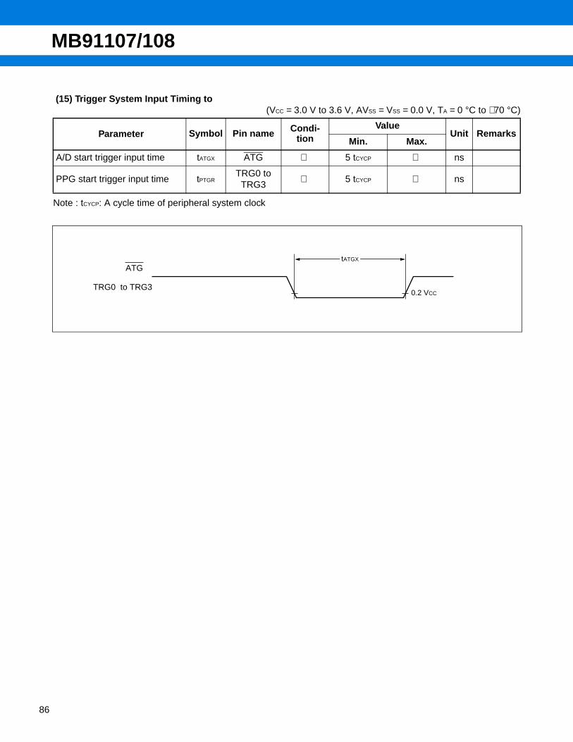
MB91107/108
86
(15) Trigger System Input Timing to (VCC = 3.0 V to 3.6 V, AVSS = VSS = 0.0 V, TA = 0 °C to +70 °C)
Note : tCYCP: A cycle time of peripheral system clock
Parameter Symbol Pin name Condi-tion
ValueUnit Remarks
Min. Max.
A/D start trigger input time tATGX ATG 5 tCYCP ns
PPG start trigger input time tPTGRTRG0 to
TRG3 5 tCYCP ns
ATG
TRG0 to TRG3
tATGX
0.2 VCC

MB91107/108
(16) DMA Controller Timing (VCC = 3.0 V to 3.6 V, AVSS = VSS = 0.0 V, TA = 0 °C to +70 °C)
Parameter Symbol Pin name Condi-tion
ValueUnit Remarks
Min. Max.
DREQ input pulse width tDRWH
DREQ0 to DREQ2
2 tCYC ns
DACK delay time(Normal bus)(Normal DRAM)
tCLDL CLKDACK0 to DACK2
6 ns
tCLDH 6 ns
EOP delay time(Normal bus)(Normal DRAM)
tCLEL CLKEOP0 to EOP2
6 ns
tCLEH 6 ns
DACK delay time(Single DRAM)(Hyper DRAM)
tCHDL CLKDACK0 to DACK2
n / 2 × tCYC ns
tCHDH 6 ns
EOP delay time(Single DRAM)(Hyper DRAM)
tCHEL CLKEOP0 to EOP2
n / 2 × tCYC ns
tCHEH 6 ns
CLK
DREQ0 to DREQ2
2.4 V 2.4 V
2.4 V 2.4 V
0.8 V
0.8 V
0.8 V 0.8 V
2.4 V
2.4 V
DACK0 to DACK2EOP0 to EOP2
DACK0 to DACK2EOP0 to EOP2(Single DRAM)(Hyper DRAM)
tCYC
tDRWH
tCLDLtCLEL
tCHDLtCHEL
tCLDHtCLEH
tCHDHtCHEH
(Normal bus) (Normal DRAM)
87
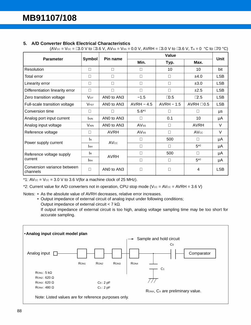
MB91107/108
88
5. A/D Converter Block Electrical Characteristics (AVCC = VCC = +3.0 V to +3.6 V, AVSS = VSS = 0.0 V, AVRH = +3.0 V to +3.6 V, TA = 0 °C to +70 °C)
*1: AVCC = VCC = 3.0 V to 3.6 V(for a machine clock of 25 MHz).
*2: Current value for A/D converters not in operation, CPU stop mode (VCC = AVCC = AVRH = 3.6 V)
Notes: • As the absolute value of AVRH decreases, relative error increases.• Output impedance of external circuit of analog input under following conditions;
Output impedance of external circuit < 7 kΩ.If output impedance of external circuit is too high, analog voltage sampling time may be too short foraccurate sampling.
Parameter Symbol Pin name Value
UnitMin. Typ. Max.
Resolution 10 10 bit
Total error ±4.0 LSB
Linearity error ±3.0 LSB
Differentiation linearity error ±2.5 LSB
Zero transition voltage VOT AN0 to AN3 −1.5 +0.5 +2.5 LSB
Full-scale transition voltage VFST AN0 to AN3 AVRH − 4.5 AVRH − 1.5 AVRH + 0.5 LSB
Conversion time 5.6*1 µs
Analog port input current IAIN AN0 to AN3 0.1 10 µA
Analog input voltage VAIN AN0 to AN3 AVSS AVRH V
Reference voltage AVRH AVSS AVCC V
Power supply currentIA
AVCC 500 µA
IAH 5*2 µA
Reference voltage supply current
IRAVRH
500 µA
IRH 5*2 µA
Conversion variance between channels AN0 to AN3 4 LSB
•Analog input circuit model plan
RON1 : 5 kΩRON2 : 620 ΩRON3 : 620 ΩRON4 : 480 Ω
C0 : 2 pF
C1 : 2 pF
RON1 RON2 RON3 RON4
C0
C1
Sample and hold circuit
Analog input Comparator
Note: Listed values are for reference purposes only.
RONX, CX are preliminary value.
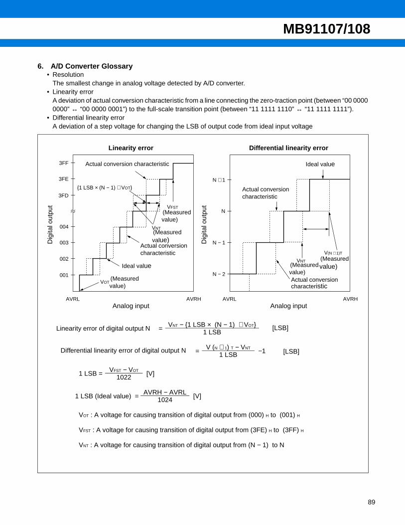
MB91107/108
6. A/D Converter Glossary• Resolution
The smallest change in analog voltage detected by A/D converter.• Linearity error
A deviation of actual conversion characteristic from a line connecting the zero-traction point (between “00 00000000” ↔ “00 0000 0001”) to the full-scale transition point (between “11 1111 1110” ↔ “11 1111 1111”).
• Differential linearity errorA deviation of a step voltage for changing the LSB of output code from ideal input voltage
3FF
3FE
3FD
004
003
002
001
AVRL AVRH
1 LSB × (N − 1) + VOT
VNT
VFST
VOT
N − 1
AVRL AVRH
N − 2
N
N + 1
VNT
V(N + 1)T
Linearity error Differential linearity error
Dig
ital o
utpu
t
Dig
ital o
utpu
t
Actual conversion characteristic
Analog input Analog input
Linearity error of digital output N = VNT − 1 LSB × (N − 1) + VOT 1 LSB
[LSB]
Differential linearity error of digital output N = V (N + 1) T − VNT
1 LSB −1
1 LSB = VFST − VOT
1022 [V]
1 LSB (Ideal value) = AVRH − AVRL1024 [V]
VOT : A voltage for causing transition of digital output from (000) H to (001) H
VFST : A voltage for causing transition of digital output from (3FE) H to (3FF) H
VNT : A voltage for causing transition of digital output from (N − 1) to N
[LSB]
Actual conversion characteristic
Actual conversion characteristic
Actual conversion characteristic
(Measured value)
(Measured value)
(Measured value)
(Measured value)
(Measured value) Ideal value
Ideal value
89
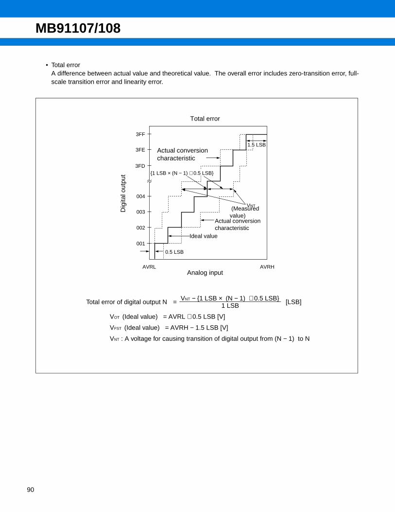
MB91107/108
90
• Total errorA difference between actual value and theoretical value. The overall error includes zero-transition error, full-scale transition error and linearity error.
VNT − 1 LSB × (N − 1) + 0.5 LSB 1 LSB
3FF
3FE
3FD
004
003
002
001
AVRL AVRH
1.5 LSB
VNT
0.5 LSB
1 LSB × (N − 1) + 0.5 LSB
Total errorD
igita
l out
put
Analog input
Total error of digital output N = [LSB]
VOT (Ideal value) = AVRL + 0.5 LSB [V]
VFST (Ideal value) = AVRH − 1.5 LSB [V]
VNT : A voltage for causing transition of digital output from (N − 1) to N
Ideal value
Actual conversion characteristic
(Measured value)
Actual conversion characteristic

MB91107/108
REFERENCE DATA
(1) “H” level output voltage (2) “L” level output voltage
“H” level output voltage vs. power supply voltage “L” level output voltage vs. power supply voltage
(3) “H” level input / “L” level input voltage
(CMOS input)
(4) “H”level input / “L” level input voltage
(Hysteresys input)
Input level vs. power supply voltage (CMOS )
Input level vs. power supply voltage (Hysteresys )
4.003.803.603.403.203.002.802.602.402.202.00
2.7 3.0 3.3 3.6 3.9
VO
H (
V)
VCC (V)
140.0
135.0
130.0
125.0
120.0
150.0
110.0
105.0
100.02.7 3.0 3.3 3.6 3.9
VO
L (V
)
VCC (V)
3.02.82.62.42.22.01.81.61.41.21.00.80.6
2.7 3.0 3.3 3.6 3.9
VIH
VIL
VCC (V)
VIN
(V
)
3.02.82.62.42.22.01.81.61.41.21.00.80.6
2.7 3.0 3.3 3.6 3.9
VIH
VIL
VCC (V)
VIN
(V
)
91
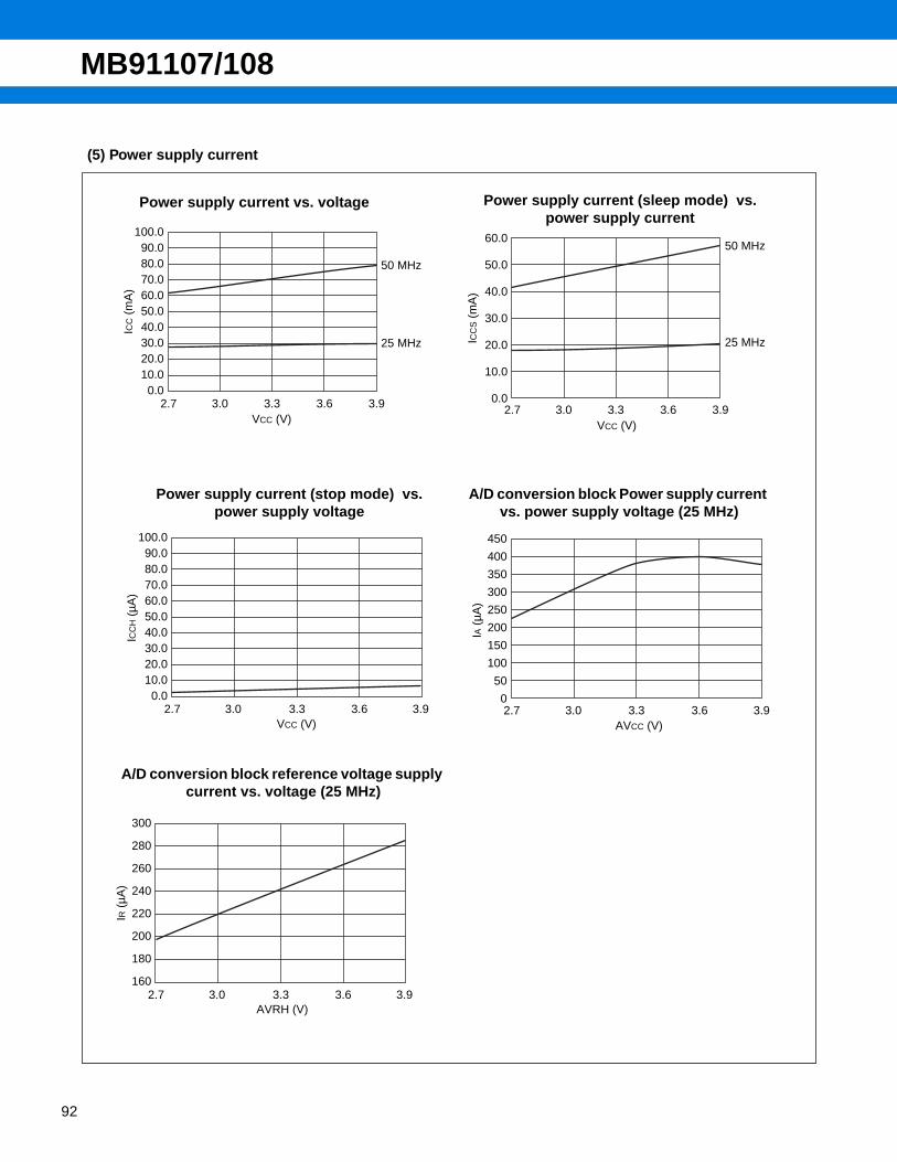
MB91107/108
92
(5) Power supply current
100.090.080.070.060.050.040.030.020.010.00.0
2.7 3.0 3.3 3.6 3.9
50 MHz
25 MHz
ICC (
mA
)
VCC (V)
Power supply current vs. voltage
60.0
50.0
40.0
30.0
20.0
10.0
0.02.7 3.0 3.3 3.6 3.9
50 MHz
25 MHzICC
S (
mA
)
VCC (V)
Power supply current (sleep mode) vs. power supply current
100.090.080.070.060.050.040.030.020.010.00.0
2.7 3.0 3.3 3.6 3.9VCC (V)
ICC
H (
µA)
Power supply current (stop mode) vs. power supply voltage
450
400
350
300
250
200
150
100
50
02.7 3.0 3.3 3.6 3.9
AVCC (V)
IA (
µA)
A/D conversion block Power supply current vs. power supply voltage (25 MHz)
300
280
260
240
220
200
180
1602.7 3.0 3.3 3.6 3.9
AVRH (V)
IR (
µA)
A/D conversion block reference voltage supply current vs. voltage (25 MHz)

MB91107/108
(6) Pull-up / pull-down resistance
100.0
10.02.7 3.0 3.3 3.6 3.9
VCC (V)
R (
Ω)
Pull-down resistance vs. power supply voltage
100.0
10.02.7 3.0 3.3 3.6 3.9
VCC (V)
R (
Ω)
Pull-up resistance vs. power supply voltage
93

MB91107/108
94
ORDERING INFORMATION
Part number Package Remarks
MB91107PFVMB91108PFV
120-pin Plastic LQFP (FPT-120P-M21)
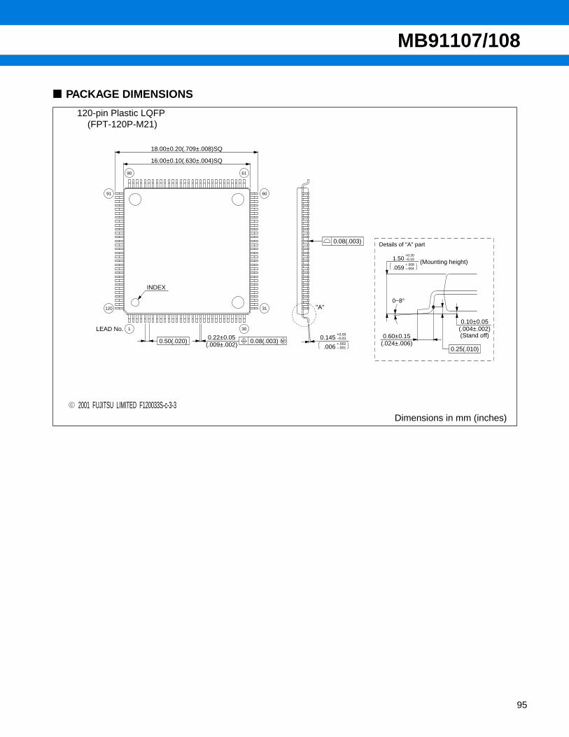
MB91107/108
PACKAGE DIMENSIONS
120-pin Plastic LQFP (FPT-120P-M21)
Dimensions in mm (inches)
C 2001 FUJITSU LIMITED F120033S-c-3-3
1 30
60
31
90 61
120
91
16.00±0.10(.630±.004)SQ
18.00±0.20(.709±.008)SQ
0.50(.020)0.22±0.05
(.009±.002)M0.08(.003)
INDEX
.006 –.001+.002
–0.03+0.05
0.145
"A"
0.08(.003)
LEAD No.
.059 –.004+.008
–0.10+0.20
1.50
Details of "A" part
0~8°
(Mounting height)
0.60±0.15(.024±.006)
0.25(.010)
(.004±.002)0.10±0.05
(Stand off)
95

MB91107/108
FUJITSU LIMITEDFor further information please contact:
Japan
FUJITSU LIMITEDMarketing DivisionElectronic DevicesShinjuku Dai-Ichi Seimei Bldg. 7-1,Nishishinjuku 2-chome, Shinjuku-ku,Tokyo 163-0721, JapanTel: +81-3-5322-3353Fax: +81-3-5322-3386http://edevice.fujitsu.com/
North and South America
FUJITSU MICROELECTRONICS AMERICA, INC.3545 North First Street,San Jose, CA 95134-1804, U.S.A.Tel: +1-408-922-9000Fax: +1-408-922-9179Customer Response CenterMon. - Fri.: 7 am - 5 pm (PST)Tel: +1-800-866-8608Fax: +1-408-922-9179http://www.fma.fujitsu.com/
Europe
FUJITSU MICROELECTRONICS EUROPE GmbHAm Siebenstein 6-10,D-63303 Dreieich-Buchschlag,GermanyTel: +49-6103-690-0Fax: +49-6103-690-122http://www.fme.fujitsu.com/
Asia Pacific
FUJITSU MICROELECTRONICS ASIA PTE. LTD.#05-08, 151 Lorong Chuan,New Tech Park,Singapore 556741Tel: +65-281-0770Fax: +65-281-0220http://www.fmal.fujitsu.com/
Korea
FUJITSU MICROELECTRONICS KOREA LTD.1702 KOSMO TOWER, 1002 Daechi-Dong,Kangnam-Gu,Seoul 135-280KoreaTel: +82-2-3484-7100Fax: +82-2-3484-7111
F0110 FUJITSU LIMITED Printed in Japan
All Rights Reserved.
The contents of this document are subject to change without notice. Customers are advised to consult with FUJITSU salesrepresentatives before ordering.
The information and circuit diagrams in this document arepresented as examples of semiconductor device applications, andare not intended to be incorporated in devices for actual use. Also,FUJITSU is unable to assume responsibility for infringement ofany patent rights or other rights of third parties arising from the useof this information or circuit diagrams.
The products described in this document are designed, developedand manufactured as contemplated for general use, includingwithout limitation, ordinary industrial use, general office use,personal use, and household use, but are not designed, developedand manufactured as contemplated (1) for use accompanying fatalrisks or dangers that, unless extremely high safety is secured, couldhave a serious effect to the public, and could lead directly to death,personal injury, severe physical damage or other loss (i.e., nuclearreaction control in nuclear facility, aircraft flight control, air trafficcontrol, mass transport control, medical life support system, missilelaunch control in weapon system), or (2) for use requiringextremely high reliability (i.e., submersible repeater and artificialsatellite).Please note that Fujitsu will not be liable against you and/or anythird party for any claims or damages arising in connection withabove-mentioned uses of the products.
Any semiconductor devices have an inherent chance of failure. Youmust protect against injury, damage or loss from such failures byincorporating safety design measures into your facility andequipment such as redundancy, fire protection, and prevention ofover-current levels and other abnormal operating conditions.
If any products described in this document represent goods ortechnologies subject to certain restrictions on export under theForeign Exchange and Foreign Trade Law of Japan, the priorauthorization by Japanese government will be required for exportof those products from Japan.