3 d fnal_gd
32
3D-IC technology for future detectors, FNAL, 02/17/2009 3D-IC technology for future detectors detectors Grzegorz Deptuch on behalf of the FERMILAB ASIC design group Raymond Yarema Grzegorz Deptuch, Jim Hoff, Farah Khalid, Marcel Trimpl, Alpana Shenai, Tom Zimmerman OUTLINE: Tom Zimmerman 1) History and introduction 2) Why 3D-IC? 3) Key components for 3D-IC technology 4) 3D IC at Fermilab 1 4) 3D-IC at Fermilab 5) Roadmaps and summary
Transcript of 3 d fnal_gd
3D-IC technology for future detectors, FNAL, 02/17/2009
3D-IC technology for future detectorsdetectors
Grzegorz Deptuch
on behalf of the FERMILAB ASIC design groupg g pRaymond YaremaGrzegorz Deptuch, Jim Hoff, Farah Khalid, Marcel Trimpl, Alpana Shenai, Tom Zimmerman
OUTLINE:
Tom Zimmerman
1) History and introduction 2) Why 3D-IC?3) Key components for 3D-IC technology 4) 3D IC at Fermilab
1
4) 3D-IC at Fermilab5) Roadmaps and summary

3D-IC technology for future detectors, FNAL, 02/17/2009
2
3D-IC technology for future detectors, FNAL, 02/17/2009
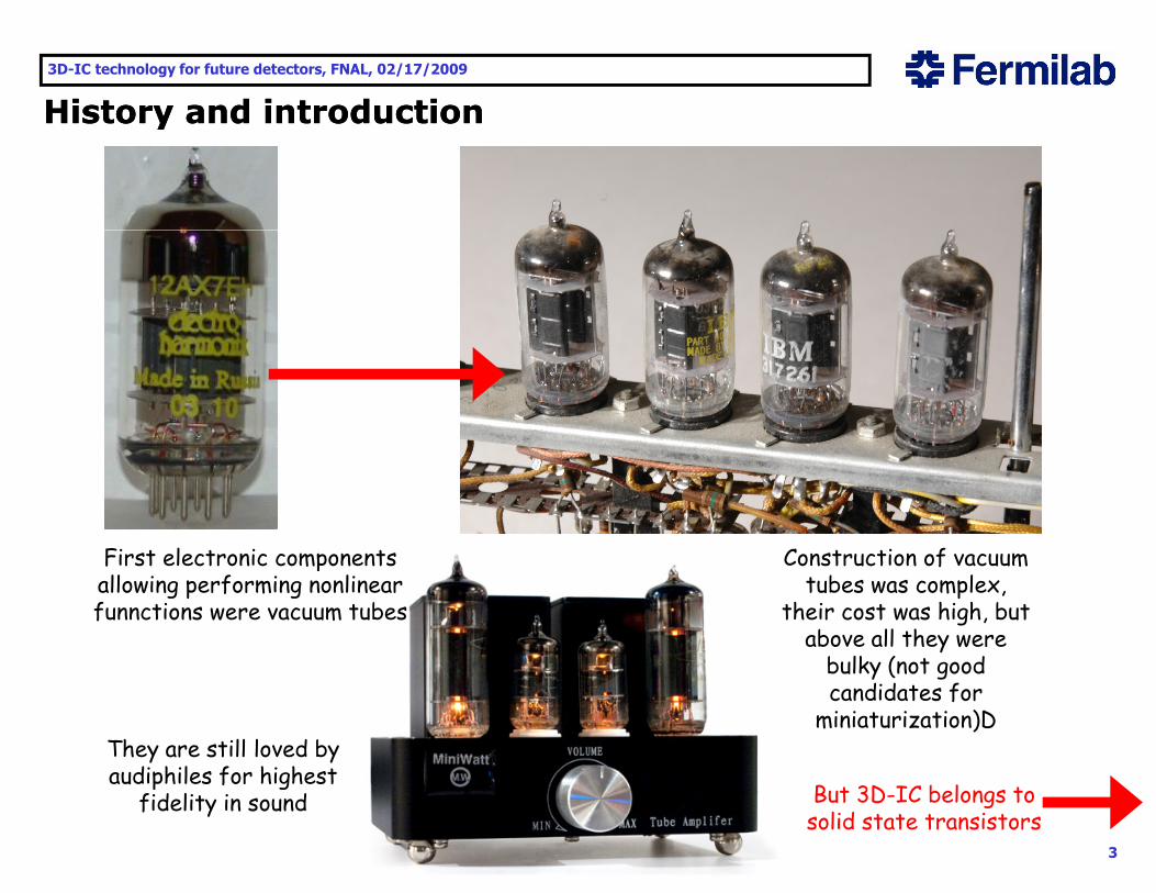
History and introductionHistory and introductionHistory and introductionHistory and introduction
First electronic components Construction of vacuum First electronic components allowing performing nonlinear funnctions were vacuum tubes
Construction of vacuum tubes was complex,
their cost was high, but above all they were
bulky (not good bulky (not good candidates for
miniaturization)DThey are still loved by audiphiles f r hi hest
3
audiphiles for highest fidelity in sound But 3D-IC belongs to
solid state transistors
3D-IC technology for future detectors, FNAL, 02/17/2009
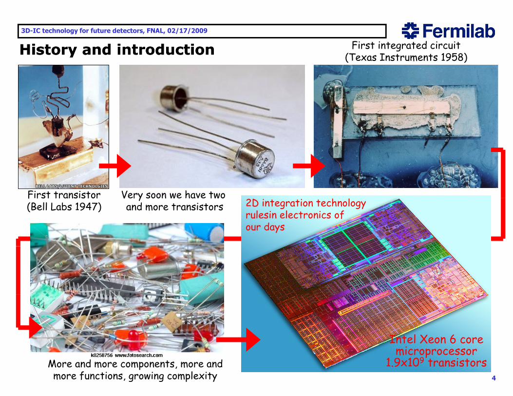
History and introductionHistory and introduction First integrated circuit (T I t t 1958)History and introductionHistory and introduction (Texas Instruments 1958)
First transistor Very soon we have two First transistor(Bell Labs 1947)
Very soon we have two and more transistors 2D integration technology
rulesin electronics of our days
Intel Xeon 6 core
4
Intel Xeon 6 core microprocessor
1.9x10⁹ transistorsMore and more components, more and more functions, growing complexity
3D-IC technology for future detectors, FNAL, 02/17/2009
History and introductionHistory and introductionHistory and introductionHistory and introduction
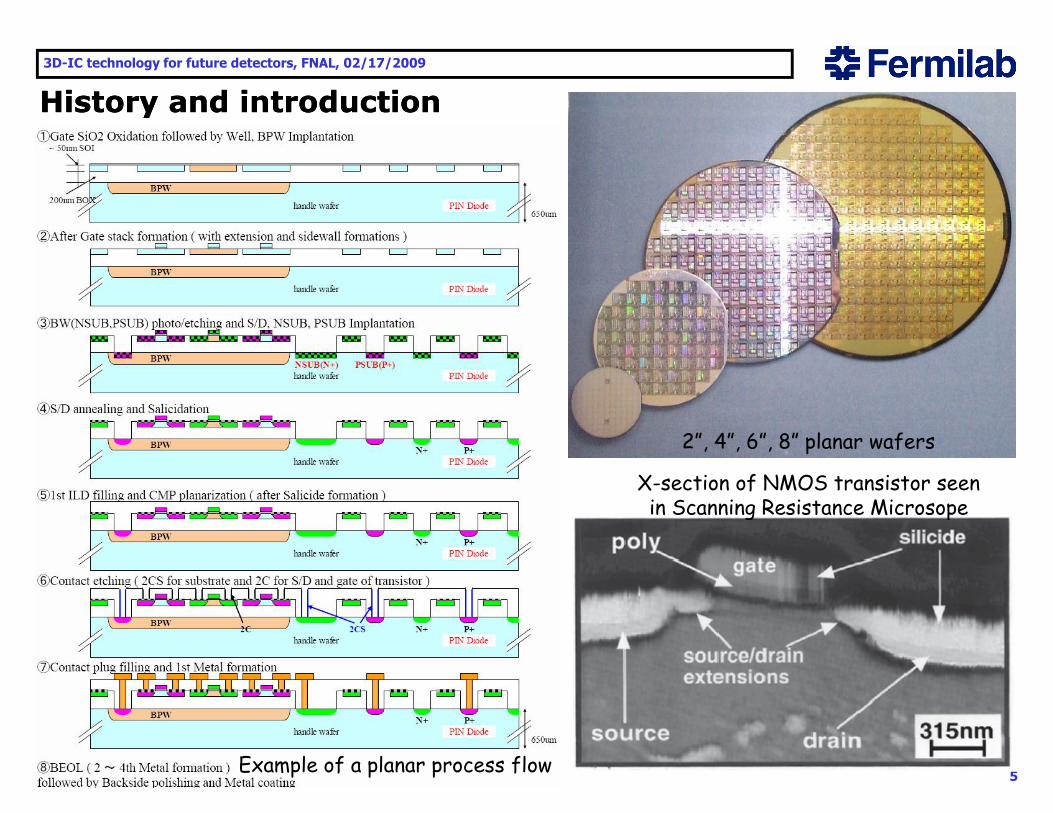
2”, 4”, 6”, 8” planar wafers
X-section of NMOS transistor seen in Scanning Resistance Microsopein Scanning Resistance Microsope
5Example of a planar process flow
3D-IC technology for future detectors, FNAL, 02/17/2009
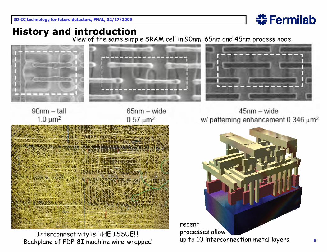
History and introductionHistory and introductionHistory and introductionHistory and introductionView of the same simple SRAM cell in 90nm, 65nm and 45nm process node
6Interconnectivity is THE ISSUE!!!
Backplane of PDP-8I machine wire-wrapped
recent processes allow up to 10 interconnection metal layers
3D-IC technology for future detectors, FNAL, 02/17/2009
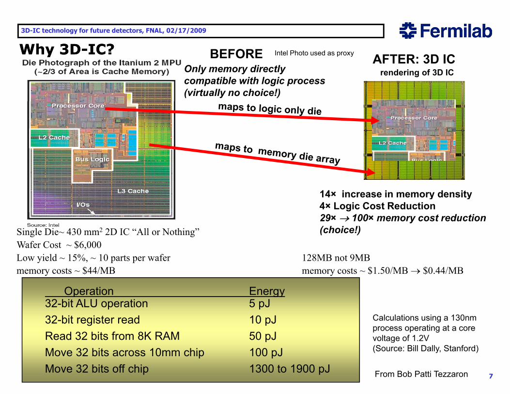
Intel Photo used as proxyBEFOREWhy 3DWhy 3D--IC?IC?rendering of 3D IC
AFTER: 3D ICIntel Photo used as proxyBEFORE Only memory directly compatible with logic process(virtually no choice!)
Why 3DWhy 3D IC?IC?
14× increase in memory density
Single Die~ 430 mm2 2D IC “All or Nothing”Wafer Cost ~ $6 000
14 increase in memory density4× Logic Cost Reduction29× → 100× memory cost reduction (choice!)
Operation Energy
Wafer Cost ~ $6,000Low yield ~ 15%, ~ 10 parts per wafer 128MB not 9MBmemory costs ~ $44/MB memory costs ~ $1.50/MB → $0.44/MB
Operation Energy32-bit ALU operation 5 pJ32-bit register read 10 pJRead 32 bits from 8K RAM 50 pJ
Calculations using a 130nm process operating at a core voltage of 1.2V
7
pMove 32 bits across 10mm chip 100 pJMove 32 bits off chip 1300 to 1900 pJ
voltage of 1.2V (Source: Bill Dally, Stanford)
From Bob Patti Tezzaron

3D-IC technology for future detectors, FNAL, 02/17/2009
Why 3DWhy 3D--IC?IC?Why 3DWhy 3D IC?IC?
improvements to achieve using 3Dimprovements to achieve using 3D--IC :IC :
reduced interconnect delays (R L C) higher clock ratesreduced interconnect delays (R L C) higher clock ratesreduced interconnect delays (R, L, C), higher clock rates,reduced interconnect delays (R, L, C), higher clock rates,reduced interconnect capacitance ( I/O pads ), lower power dissipation,reduced interconnect capacitance ( I/O pads ), lower power dissipation,higher integration density, may go heterogeneoushigher integration density, may go heterogeneoushigh bahigh banndwidth dwidth μμ--processorsprocessorsmerging different process technologies, mixed materials, system integration,merging different process technologies, mixed materials, system integration,advanced focal planesadvanced focal planesadvanced focal planesadvanced focal planes
8
Optimal repartition of functions
3D-IC technology for future detectors, FNAL, 02/17/2009
Why 3DWhy 3D--IC?IC?Why 3DWhy 3D IC?IC?3D3D
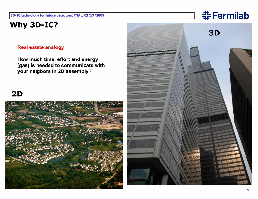
Real estate analogy
How much time, effort and energy (gas) is needed to communicate with your neigbors in 2D assembly?
2D2D
9
3D-IC technology for future detectors, FNAL, 02/17/2009
Key components of 3DKey components of 3D--IC technologyIC technologyKey components of 3DKey components of 3D IC technologyIC technology
A chip in A chip in threethree--dimensional integrated circuit (3Ddimensional integrated circuit (3D--IC) IC) technology technology is is 3D3D--IC definitionIC definition
composedcomposed ofof two or more layers of active electronic components, two or more layers of active electronic components, integrated both vertically and horizontallyintegrated both vertically and horizontally
3D3D--IC methodsIC methods3D3D--IC methodsIC methods
Agressive wafer thinning, through wafer/chip connectivity, backAgressive wafer thinning, through wafer/chip connectivity, back--side side metalization and patterning, oxide or metal bonding (Wmetalization and patterning, oxide or metal bonding (W--W, CW, C--W, CW, C--C)C)p g, g (p g, g ( ,, ,, ))
Fermilab position in 3DFermilab position in 3D--ICICFermilab began exploring the technologies for Fermilab began exploring the technologies for 3D3D circuits in 2006. circuits in 2006. Fermilab is leading an Int’l Consortium (15 members) on 3DFermilab is leading an Int’l Consortium (15 members) on 3D--IC for IC for
scientific applications, mainly HEPscientific applications, mainly HEP
h //3di f l
N t l ‘t i t /N t l ‘t i t / 22’ b t 3D’ b t 3D IC th d l dIC th d l d tt l t fl t f
Importance of 3DImportance of 3D--IC in detectorsIC in detectors
http://3dic.fnal.gov
10
Not only more ‘transistors/Not only more ‘transistors/μμmm22’, but 3D’, but 3D--IC methods lead IC methods lead to to replacement ofreplacement oftypictypical bumpal bump bonds bonds and open new frontiers for detectors architecturesand open new frontiers for detectors architectures

3D-IC technology for future detectors, FNAL, 02/17/2009
Key components of 3DKey components of 3D--IC technologyIC technologyKey components of 3DKey components of 3D IC technologyIC technology
THROUGH SILICON VIAS (TSV)THROUGH SILICON VIAS (TSV)
11proxy picture
3D-IC technology for future detectors, FNAL, 02/17/2009
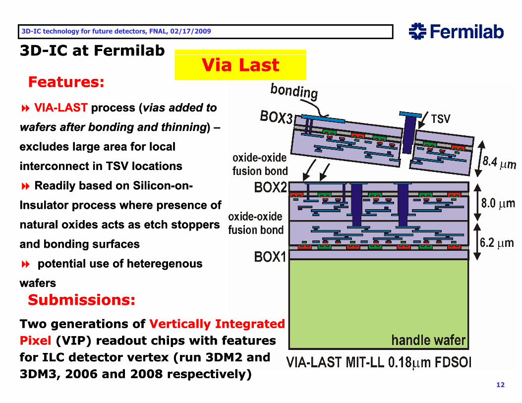
3D3D--IC at FermilabIC at FermilabVia LastVia Last
VIAVIA LASTLAST (( i dd d ti dd d t
Features:Features:
3D3D IC at FermilabIC at Fermilab
VIAVIA--LASTLAST process (process (vias added to vias added to wafers after bonding and thinningwafers after bonding and thinning)) ––excludes large area for local excludes large area for local gginterconnect in TSV locationsinterconnect in TSV locations
Readily based on SiliconReadily based on Silicon--onon--I l t h fI l t h fInsulator process where presence of Insulator process where presence of natural oxides acts as etch stoppers natural oxides acts as etch stoppers and bonding surfacesand bonding surfaces
potential use of heteregenous potential use of heteregenous waferswafersSubmissions:Submissions:
Two generations of Two generations of Vertically Integrated Vertically Integrated PixelPixel (VIP) readout chips with features (VIP) readout chips with features
Submissions:Submissions:
12
for ILC detector vertex (run 3DM2 and for ILC detector vertex (run 3DM2 and 3DM3, 2006 and 2008 respectively)3DM3, 2006 and 2008 respectively)
3D-IC technology for future detectors, FNAL, 02/17/2009
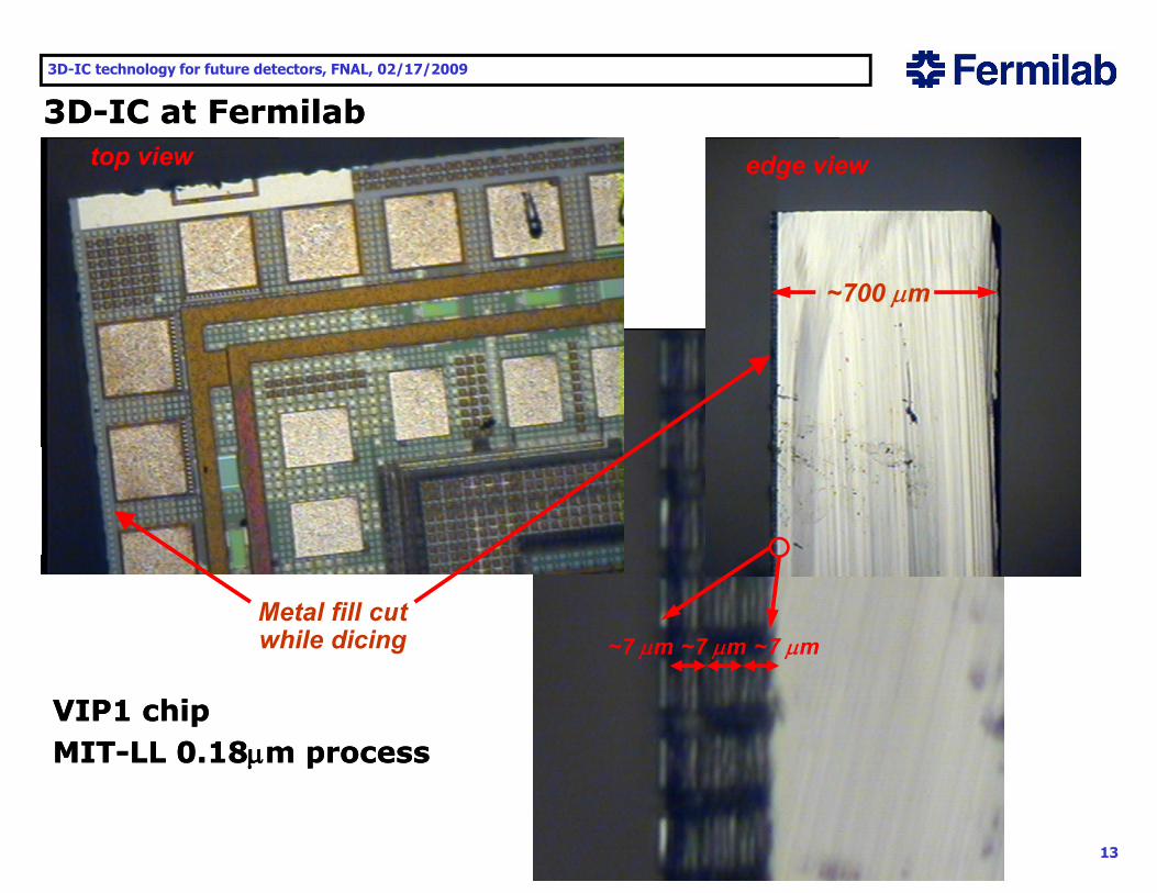
3D3D--IC at FermilabIC at Fermilab
edge view top view 3D3D IC at FermilabIC at Fermilab
~700 μm
Metal fill cut while dicing ~7 μm~7 μm~7 μm
VIP1 chip VIP1 chip MITMIT--LL 0.18LL 0.18μμm processm process
13

3D-IC technology for future detectors, FNAL, 02/17/2009
3D3D--IC at FermilabIC at Fermilab3D3D IC at FermilabIC at Fermilab
VIAVIA--FIRSTFIRST process (vias process (vias are part of the are part of the Features:Features:
Via FirstVia First
wafer processing inserted before or wafer processing inserted before or right after forming transistorsright after forming transistors) ) ––metal interconnect lines are not excludedmetal interconnect lines are not excludedmetal interconnect lines are not excluded metal interconnect lines are not excluded over over TSV locationsTSV locations (TSVs 1.3 (TSVs 1.3 μμm diameter, m diameter, 3.8 3.8 μμm rec. spacing and 6 m rec. spacing and 6 μμm depth),m depth),
8” wafers, large ~268” wafers, large ~26××31 mm31 mm22 reticule, reticule, W W 66thth metal used as a bond interface for metal used as a bond interface for
faceface faceface CuCu Cu thermoCu thermo compressioncompressionfaceface--face face CuCu--Cu thermoCu thermo--compressioncompressionbondingbonding
Submissions:Submissions:3 fully functional prototypes from 3 fully functional prototypes from Fermilab together with 9 other Fermilab together with 9 other subreticules from participating subreticules from participating
14
p p gp p ginstitutions submitted on a Fermi institutions submitted on a Fermi MPW run in 2009; MPW run in 2009; currently ‘in fab’currently ‘in fab’
0.13 0.13 μμm bulk CMOS by Chartered with m bulk CMOS by Chartered with TezzaronTezzaron 3D via3D via--first technologyfirst technology
11

3D-IC technology for future detectors, FNAL, 02/17/2009
3D3D--IC at FermilabIC at Fermilab3D3D IC at FermilabIC at Fermilab• Access to the first commercially available 3D-IC process through Tezzaron
excited creation of a consortium centered on Fermilab in late 2008. The consortium groups international laboratories and universities with interest in
Consortium presently comprised of 15 members from 5 countries
consortium groups international laboratories and universities with interest in High Energy Physics for the development of 3D integrated circuits.
– University at Bergamo
– University at Pavia– University of Bonn– AGH University of
S i &T h l – University at Perugia– INFN Bologna– INFN at Pisa
Science &Technology, Poland
– Fermilab, Batavia
– INFN at Rome– CPPM, Marseilles– IPHC, Strasbourg
• Others contributing to first MPW
BNL BrookhavenIPHC, Strasbourg– IRFU Saclay– LAL, Orsay– LPNHE Paris
– BNL, Brookhaven– LBNL, Berkeley
15
– LPNHE, Paris– CMP, Grenoble http://3dic.fnal.gov

3D-IC technology for future detectors, FNAL, 02/17/2009
3D3D--IC at FermilabIC at Fermilab
• 3D chip has two tiers• One set of masks used for both
top and bottom tiers to reduce
3D3D IC at FermilabIC at Fermilab
top and bottom tiers to reduce mask cost.– Identical wafers bonded face to
face by Tezzaron.Backside metallization by – Backside metallization by Tezzaron.
• Frame divided into 12 subreticules among consortium
bmembers• More than 25 two-tier designs
(circuits and test devices)– CMS strips, ATLAS pixels
TX1 TX2TY1 TY2
A1 B1 B2 A2
C1 D1 D2 C2
TXL TXRTYL TYR
AL BL BR AR
DL DR CRCMS strips, ATLAS pixels– ILC pixels – B factory pixels– X-ray imaging
T t i it
E1 F1 F2 F2
G1 H1 H2 G2
J1 K1 K2 J2
TX1 TX2TY1 TY2
A1 B1 B2 A2
C1 D1 D2 C2
E1 F1 F2 F2
G1 H1 H2 G2
J1 K1 K2 J2
CL DL DR CR
EL FL FR ER
GL HL HR GR– Test circuits• Radiation• Cryogenic operation• Via and bonding reliability
Frame layout
Max frame layout area includinginternal saw streets: x=25.760 mmy= 30.260 mm.
GL HL HR GR
JL JRIL IR
16
• SEU tolerance Wafer Map

3D-IC technology for future detectors, FNAL, 02/17/2009
3D3D--IC at FermilabIC at FermilabTest chips:TX, TY2.0 x 6.3 mm
– frame organization:• Top and bottom tiers
fabricated on the same frame; vertical symmetry about the center of the
3D3D IC at FermilabIC at Fermilab
about the center of the frame for flipping one wafer over another and obtaining matching of circuits in 3D assembly,
• All designs initially submitted by mid-May2009
– Fermilab designsSubreticules:A, B, C, D, E, F, G, H, I, J5.5 x 6.3 mm
Fermilab designs • H = VICTR; short pixel
readout chips realizing pt cut for implementation of L1 trigger embedded in t k f CMS @ SLHC
Full frame
tracker for CMS @ SLHC• I = VIP2b; time stamping
pixel readout chip for vertex detector @ ILC
• J = VIPIC; very high frame0.13 μm Chartered
• J = VIPIC; very high frame rate with sparsification pixel readout chip for X-ray Photon Correlation Spectroscopy @ light source
H H*
17Top tiers Bottom Tiers
sourceJI J* I*
3D-IC technology for future detectors, FNAL, 02/17/2009
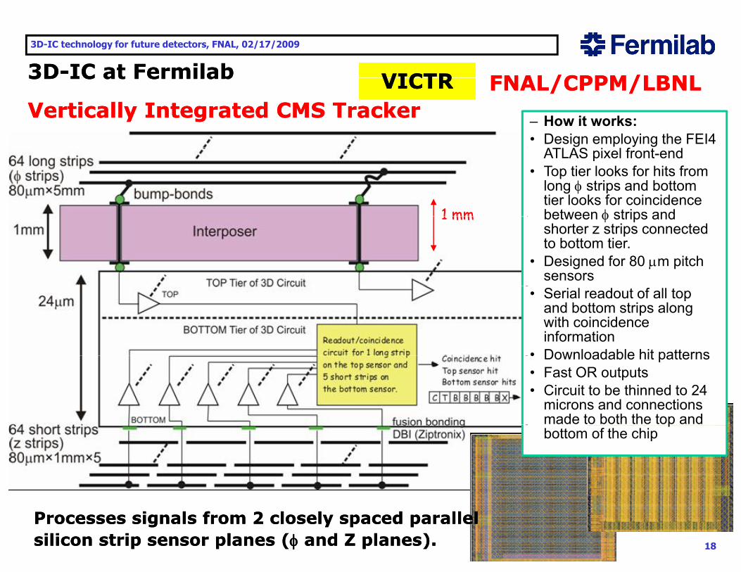
VICTRVICTR FNAL/CPPM/LBNLFNAL/CPPM/LBNL3D3D--IC at FermilabIC at Fermilab VICTRVICTRVertically Integrated CMS TrackerVertically Integrated CMS Tracker
FNAL/CPPM/LBNLFNAL/CPPM/LBNL
– How it works:• Design employing the FEI4
3D3D IC at FermilabIC at Fermilab
ATLAS pixel front-end• Top tier looks for hits from
long φ strips and bottom tier looks for coincidence between φ strips and1 mm between φ strips and shorter z strips connected to bottom tier.
• Designed for 80 μm pitch sensors
1 mm
• Serial readout of all top and bottom strips along with coincidence information
• Downloadable hit patterns• Downloadable hit patterns• Fast OR outputs• Circuit to be thinned to 24
microns and connections made to both the top and pbottom of the chip
18
Processes signals from 2 closely spaced parallel Processes signals from 2 closely spaced parallel silicon strip sensor planes (silicon strip sensor planes (φφ and Z planes).and Z planes).

3D-IC technology for future detectors, FNAL, 02/17/2009
VIP2BVIP2B3D3D--IC at FermilabIC at Fermilab VIP2BVIP2B – How it works:• Adapted from earlier MITLL designs in
FDSOI technology• 192 × 192 array of 24 μm2 pixels
Vertically Integrated PixelVertically Integrated PixelVIP Functional block diagram
3D3D IC at FermilabIC at Fermilab
• 8 bit digital time stamp (Δt=3.9 μs)• Readout between ILC bunch trains of
sparsified data• Sparsification based on token passing
schemescheme• Single stage signal integrating front-end
with 2 S/H circuits for analog signal output with CDS
• Analog information available for improvedAnalog information available for improved resolution
• Separate test input for every pixel cell• Serial output bus• Polarity switch for collection of e- or h+Polarity switch for collection of e or h
signals signals are accumulated are accumulated and time stamped using and time stamped using
l b l G d t l b l G d t
19
global Grey code counter global Grey code counter

3D-IC technology for future detectors, FNAL, 02/17/2009
3D3D--IC at FermilabIC at Fermilab VIPIC VIPIC Common effort of: Common effort of: 3D3D IC at FermilabIC at Fermilab
cur_sel<3..0>
VIPIC VIPIC Common effort of: Common effort of: FNAL/BNL and FNAL/BNL and
USTUST--AGH PolandAGH PolandVertically Integrated Photon Imaging ChipVertically Integrated Photon Imaging Chip
64
0
65
1
66
2
67
3
68
4
69
5
126
191
127
192outp<15>al
izer
– How it works:• X-ray Photon
Correlation S t (XPCS)646566676869126127Group
<15>outn<15>
seria Spectroscopy (XPCS)
is a technique that is used at X-ray light sources to generate speckle patterns for
Group<1>
the study of thedynamics in various equilibrium and non-equilibrium processes
• The chip is divided in
outp<0>64 ze
r
0
65
1
66
2
67
3
68
4
69
5
126
62
127
63
The chip is divided in 16 group of 256 pixels read out in parallel but through separate LVDS serial ports D t ifi ti i
192
outn<0>128 se
riali
191
129
190
130
189
131
188
132
187
133
254
190
255
191
LVDSDRV
Group<0>
• Data sparsification is performed in each group
20Top view - bump bonding pads on the back of the digital tier
al_C
lkes
tart
DRV
3D-IC technology for future detectors, FNAL, 02/17/2009
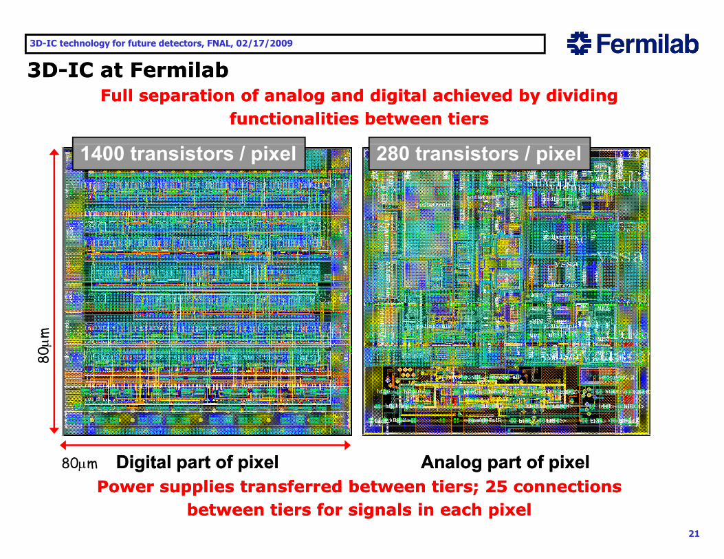
3D3D--IC at FermilabIC at Fermilab3D3D IC at FermilabIC at FermilabFull separation of analog and digital achieved by dividing Full separation of analog and digital achieved by dividing
functionalities between tiersfunctionalities between tiers
1400 transistors / pixel 280 transistors / pixel
0μm
80
Digital part of pixelDigital part of pixel Analog part of pixelAnalog part of pixelPo e s pplies t ansfe ed bet een tie s 25 connections Po e s pplies t ansfe ed bet een tie s 25 connections
80μm
21
Power supplies transferred between tiers; 25 connections Power supplies transferred between tiers; 25 connections between tiers for signals in each pixelbetween tiers for signals in each pixel
3D-IC technology for future detectors, FNAL, 02/17/2009
3D3D--IC at FermilabIC at Fermilab3D3D IC at FermilabIC at Fermilab
22
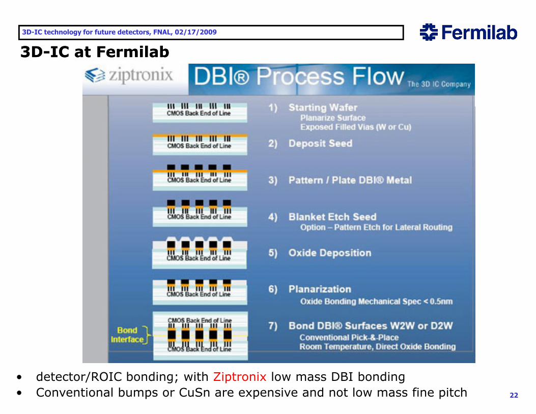
• detector/ROIC bonding; with Ziptronix low mass DBI bonding • Conventional bumps or CuSn are expensive and not low mass fine pitch
3D-IC technology for future detectors, FNAL, 02/17/2009
3D3D--IC at FermilabIC at Fermilab3D3D IC at FermilabIC at Fermilab
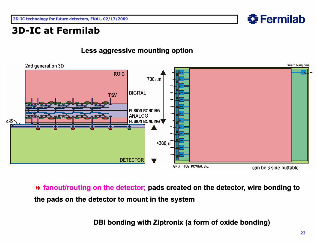
Less aggressive mounting optionLess aggressive mounting option
fanout/routing on the detector;fanout/routing on the detector; pads created on the detector, wire bonding to pads created on the detector, wire bonding to the pads on the detector to mount in the system the pads on the detector to mount in the system
23
DBI bonding with Ziptronix (a form of oxide bonding)DBI bonding with Ziptronix (a form of oxide bonding)
3D-IC technology for future detectors, FNAL, 02/17/2009
3D3D--IC at FermilabIC at Fermilab3D3D IC at FermilabIC at Fermilab
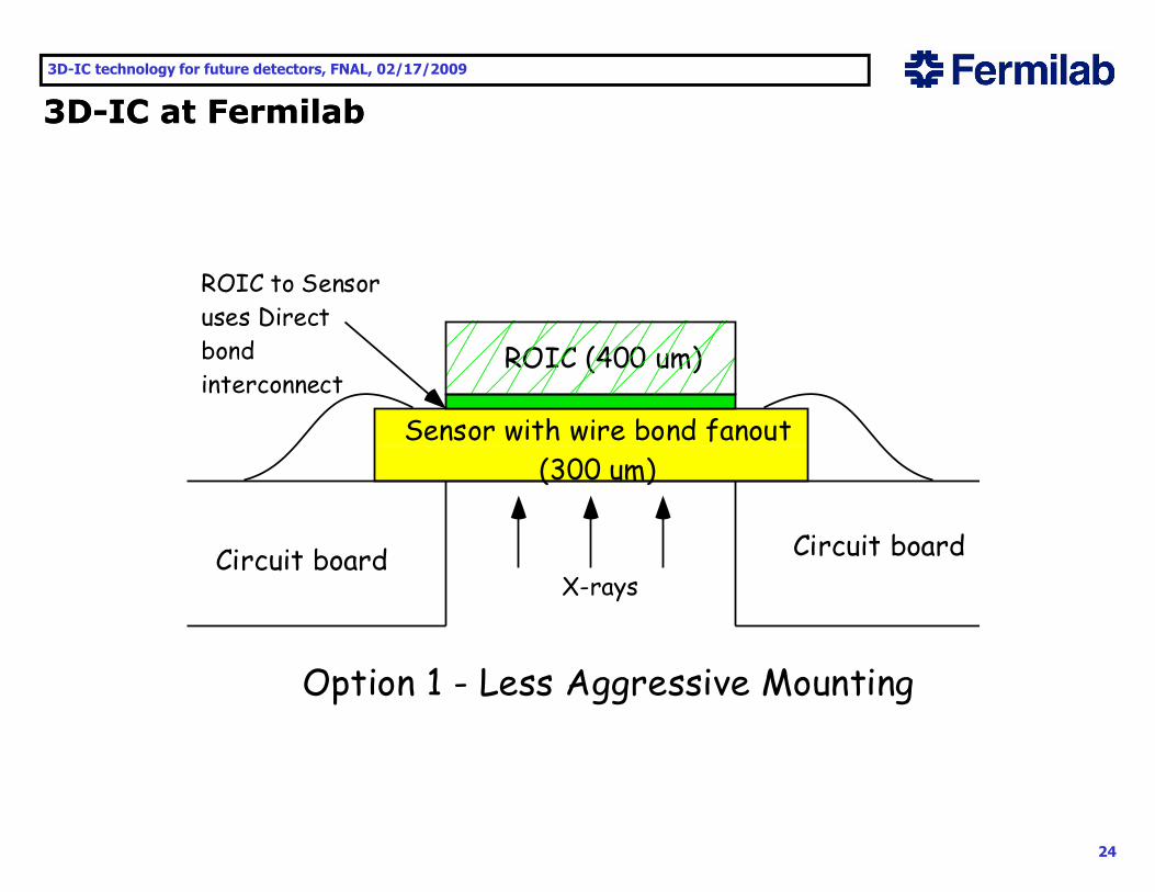
ROIC to Sensoruses Direct
Sensor with wire bond fanout
ROIC (400 um)bondinterconnect
(300 um)
Ci it b d Circuit boardCircuit board Circuit boardX-rays
Option 1 - Less Aggressive Mounting
24

3D-IC technology for future detectors, FNAL, 02/17/2009
3D3D--IC at FermilabIC at Fermilab3D3D IC at FermilabIC at Fermilab
Ultimate goal is:Ultimate goal is:fi t 4fi t 4 id b tt bl d t t tid b tt bl d t t t
aggressive mounting option aggressive mounting option –– essence of 3Dessence of 3D--IC IC
first 4first 4--side buttable detector system side buttable detector system
low density array of I/O pads available on the side of the readout chip low density array of I/O pads available on the side of the readout chip --opposite to the detector;opposite to the detector; one side of the readout chip connected to the detector one side of the readout chip connected to the detector using DBI or similar bonding technique second side used to mount the deviceusing DBI or similar bonding technique second side used to mount the device
25
using DBI or similar bonding technique, second side used to mount the device using DBI or similar bonding technique, second side used to mount the device on the support PCB with bump or stud bonding techniqueon the support PCB with bump or stud bonding technique

3D-IC technology for future detectors, FNAL, 02/17/2009
3D3D--IC at FermilabIC at Fermilab
X
3D3D IC at FermilabIC at Fermilab
X-rays
Sensor (300 um)Sensor to PCBuses bump bonds
ROIC is 25 um thickafter thinning
Circuit board
Option 2 - More Aggressive Mountingfor four side buttable sensor arrays
26

3D-IC technology for future detectors, FNAL, 02/17/2009
3D3D--IC roadmapIC roadmap3D3D IC roadmapIC roadmap
27
3D-IC technology for future detectors, FNAL, 02/17/2009
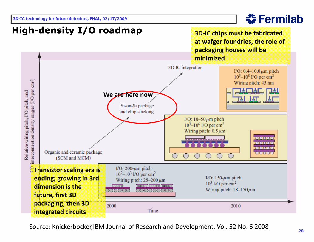
HighHigh--density I/O roadmapdensity I/O roadmap 3D IC chips must be fabricatedHighHigh density I/O roadmapdensity I/O roadmap 3D‐IC chips must be fabricated at wafger foundries, the role of packaging houses will be minimized
We are here now
Transistor scaling era is ending; growing in 3rdending; growing in 3rd dimension is the future, first 3D packaging, then 3D
d
28Source: Knickerbocker,IBM Journal of Research and Development. Vol. 52 No. 6 2008
integrated circuits
3D-IC technology for future detectors, FNAL, 02/17/2009
Summary Summary Summary Summary
3D-IC offers new approaches to old problems in detector development. New high density circuit bonding techniques, wafer thinning, and sub m size TSVs provide new opportunities for the detector designerFermilab has been working with two different vendors for 3D chipfabrication. MIT LL is a via last SOI process using oxide wafer bonding. Tezzaron i i fi CMOS i C C f b di
sub-μm size TSVs provide new opportunities for the detector designer.
is a via first CMOS process using Cu-Cu wafer bonding.
Recently a new (third) 3D-IC technique has been explored with a new pixel chip submission to the OKI-SOI run within the SOIPIX collaboration that is based in KEK, Japan. The new bonding is based on ZyCube.
Chips are still in fab, except the first device, VIP1, that was fabricated in 2007; The prototype was tested and despite poor yield actual functionality was demonstratedprototype was tested and despite poor yield actual functionality was demonstrated
The 3D-IC seems to be the avenue for future development in l i i d h b bl i i R&Dμelectronics industry we hope to be able to maintain our R&D program
Packaging industry is under revolution because of the transistor
29
g g y
scaling era is ending and 3D-IC era with TSVs is beginning.
3D-IC technology for future detectors, FNAL, 02/17/2009
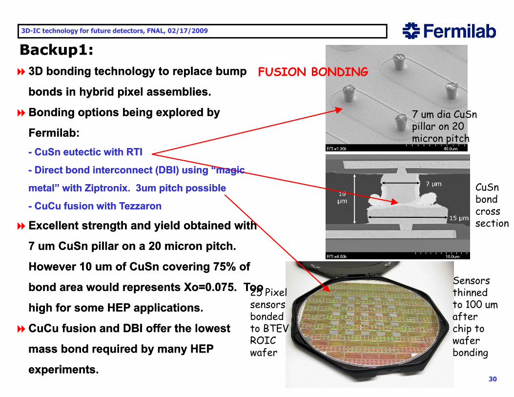
Backup1:Backup1:Backup1:Backup1:3D bonding technology to replace bump 3D bonding technology to replace bump
bonds in hybrid pixel assemblies.bonds in hybrid pixel assemblies.FUSION BONDING
7 um dia CuSnpillar on 20micron pitch
Bonding options being explored by Bonding options being explored by
FermilabFermilab::CuSn eutectic with RTICuSn eutectic with RTI
CuSnbond
-- CuSn eutectic with RTICuSn eutectic with RTI
-- Direct bond interconnect (DBI) using “magic Direct bond interconnect (DBI) using “magic
metal” with Ziptronix. 3um pitch possiblemetal” with Ziptronix. 3um pitch possiblebond cross section
-- CuCu fusion with TezzaronCuCu fusion with Tezzaron
Excellent strength and yield obtained with Excellent strength and yield obtained with
7 um CuSn pillar on a 20 micron pitch7 um CuSn pillar on a 20 micron pitch
25 PixelSensorsthinned
7 um CuSn pillar on a 20 micron pitch. 7 um CuSn pillar on a 20 micron pitch.
However 10 um of CuSn covering 75% of However 10 um of CuSn covering 75% of
bond area would represents Xo=0.075. Too bond area would represents Xo=0.075. Too 25 Pixelsensorsbonded to BTEVROIC
thinned to 100 umafter chip towafer
high for some HEP applications.high for some HEP applications.
CuCu fusion and DBI offer the lowest CuCu fusion and DBI offer the lowest
30
ROICwafer
waferbondingmass bond required by many HEP mass bond required by many HEP
experiments.experiments.
3D-IC technology for future detectors, FNAL, 02/17/2009
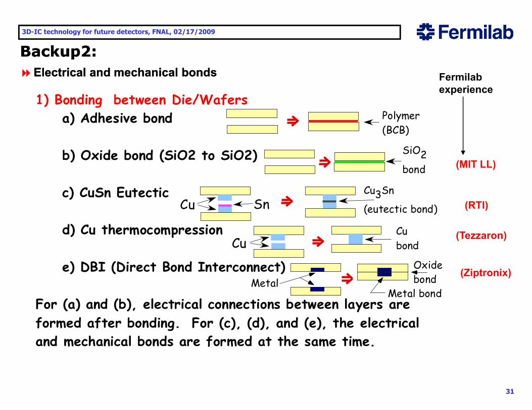
Backup2:Backup2:Backup2:Backup2:
1) Bonding between Die/Wafers
Fermilabexperience
Electrical and mechanical bondsElectrical and mechanical bonds
) ga) Adhesive bond
b) Oxide bond (SiO2 to SiO2)
Polymer(BCB)
SiO2b) Oxide bond (SiO2 to SiO2)
c) CuSn Eutectic
2bond
Cu SnCu3Sn
( i b d)
(MIT LL)
(RTI)
d) Cu thermocompression
Cu Sn (eutectic bond)
CuCubond
(RTI)
(Tezzaron)
e) DBI (Direct Bond Interconnect)
For (a) and (b) electrical connections between layers areMetal
Oxidebond
Metal bond
(Ziptronix)
For (a) and (b), electrical connections between layers areformed after bonding. For (c), (d), and (e), the electricaland mechanical bonds are formed at the same time.
31
3D-IC technology for future detectors, FNAL, 02/17/2009
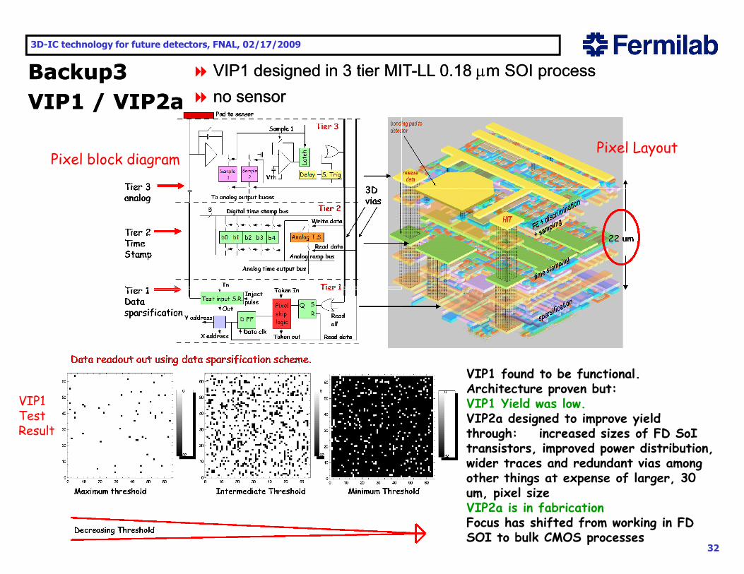
VIP1 designed in 3 tier MITVIP1 designed in 3 tier MIT--LL 0.18 LL 0.18 μμm SOI processm SOI processBackup3Backup3
Pixel Layout
gg μμ ppno sensorno sensor
Backup3Backup3VIP1 / VIP2aVIP1 / VIP2a
Pixel block diagramPixel Layout
VIP1 found to be functional. Architecture proven but:VIP1 Yield was low.VIP2a designed to improve yield
VIP1TestR lt through: increased sizes of FD SoI
transistors, improved power distribution, wider traces and redundant vias among other things at expense of larger, 30 um, pixel size
Result
32
um, pixel sizeVIP2a is in fabricationFocus has shifted from working in FD SOI to bulk CMOS processes