3-Axis Digital AccelerometerRT3000B=RT3000C/DS... · 3-Axis Digital Accelerometer General...
23
RT3000A/B/C ® DS3000ABC-00 May 2016 www.richtek.com 3 © Copyright 2016 Richtek Technology Corporation. All rights reserved. is a registered trademark of Richtek Technology Corporation. 3-Axis Digital Accelerometer General Description The RT3000 is a low power and high accuracy 3 axis acceleration sensor with digital output for portable device. The part has user selectable full scales rages of ±2g, ±4g, ±8g and ±16g, and, it is capable of measuring accelerations with output data rates from 1Hz to 200Hz. The RT3000A is available in MQFN-16L 3x3, RT3000B in MQFN-12L 2x2 (COL) and RT3000C in MDFN-10L 3x3 package. Features User programmable ±2g/±4g/±8g/±16g Full-Scale I 2 C Digital I/O Interface User Programmable Operation Modes : Power Down, Normal Mode and High Resolution Mode Programmable Interrupts For Motion and Orientation Detections Embedded FIFO Self-Test Function Applications Smartphones Tablet PC Notebook PND GPS Remote Controller Gaming Toys Ordering Information Note : Richtek products are : RoHS compliant and compatible with the current require ments of IPC/JEDEC J-STD-020. Suitable for use in SnPb or Pb-free soldering processes. Pin Configurations (TOP VIEW) MQFN-12L 2x2 (COL) MQFN-16L 3x3 RT3000 Package Type QM : MQFN-16L 3x3 (M-Type) QM : MQFN-12L 2x2 (COL) (M-Type) QM : MDFN-10L 3x3 (M-Type) Operating Temperature Range G : Green (Halogen Free and Pb Free) A : MQFN-16L 3x3 B : MQFN-12L 2x2 (COL) C : MDFN-10L 3x3 Marking Information 8E=YM DNN 8E= : Product Code YMDNN : Date Code RT3000AGQM 3P : Product Code W : Date Code 3PW RT3000BGQM 9F=YM DNN 9F= : Product Code YMDNN : Date Code RT3000CGQM MDFN-10L 3x3 VDDIO NC SCL NC SDA NC NC VDD NC GND NC INT1 RES INT2 NC NC 14 16 8 6 13 12 10 9 1 2 4 5 RES 17 11 3 15 7 NC RES VDDIO SDA GND GND INT1 INT2 SCL NC NC VDD 6 5 12 11 1 2 3 10 9 8 4 7 NC RES INT1 GND VDD NC VDDIO NC SCL SDA 5 4 3 2 1 10 9 8 7 6 RES 11
Transcript of 3-Axis Digital AccelerometerRT3000B=RT3000C/DS... · 3-Axis Digital Accelerometer General...

RT3000A/B/C®
DS3000ABC-00 May 2016 www.richtek.com3
©Copyright 2016 Richtek Technology Corporation. All rights reserved. is a registered trademark of Richtek Technology Corporation.
3-Axis Digital Accelerometer
General Description
The RT3000 is a low power and high accuracy 3 axis
acceleration sensor with digital output for portable device.
The part has user selectable full scales rages of ±2g, ±4g,
±8g and ±16g, and, it is capable of measuring accelerations
with output data rates from 1Hz to 200Hz. The RT3000A
is available in MQFN-16L 3x3, RT3000B in MQFN-12L
2x2 (COL) and RT3000C in MDFN-10L 3x3 package.
Features User programmable ±±±±±2g/±±±±±4g/±±±±±8g/±±±±±16g Full-Scale
I2C Digital I/O Interface
User Programmable Operation Modes : Power
Down, Normal Mode and High Resolution Mode
Programmable Interrupts For Motion and
Orientation Detections
Embedded FIFO
Self-Test Function
Applications Smartphones
Tablet PC
Notebook
PND
GPS
Remote Controller
Gaming
Toys
Ordering Information
Note :
Richtek products are :
RoHS compliant and compatible with the current require ments of IPC/JEDEC J-STD-020.
Suitable for use in SnPb or Pb-free soldering processes.
Pin Configurations(TOP VIEW)
MQFN-12L 2x2 (COL)MQFN-16L 3x3
RT3000Package TypeQM : MQFN-16L 3x3 (M-Type)QM : MQFN-12L 2x2 (COL) (M-Type)QM : MDFN-10L 3x3 (M-Type)
Operating Temperature RangeG : Green (Halogen Free and Pb Free)
A : MQFN-16L 3x3B : MQFN-12L 2x2 (COL)C : MDFN-10L 3x3
Marking Information
8E=YMDNN
8E= : Product Code
YMDNN : Date Code
RT3000AGQM
3P : Product Code
W : Date Code3PW
RT3000BGQM
9F=YMDNN
9F= : Product Code
YMDNN : Date Code
RT3000CGQM
MDFN-10L 3x3
VDDIO
NC
SCL
NC
SD
A
NC
NC
VD
D
NC
GND
NC
INT1
RES INT2
NC
NC
1416
86
13
12
10
9
1
2
4
5
RES
17
113
15
7
NC RES
VDDIO
SDA
GND
GND
INT
1
INT
2
SC
L
NC
NC VDD65
12 111
2
3
10
9
8
4 7
NC
RES
INT1
GND
VDD
NC
VDDIO
NC
SCL
SDA
5
4
3
2
1 10
9
8
7
6
RES
11

RT3000A/B/C
2
DS3000ABC-00 May 2016www.richtek.com
©Copyright 2016 Richtek Technology Corporation. All rights reserved. is a registered trademark of Richtek Technology Corporation.
Function Pin DescriptionRT3000A (MQFN-16L 3x3) Name Description
14 VDD Power Supply.
1 VDDIO Power Supply For I/O Pins.
12 GND Ground.
6 SDA I2C Serial Data.
4 SCL I2C Serial Clock.
9 INT1 Interrupt 1.
11 INT2 Interrupt 2.
2, 5, 7, 8, 10, 13, 15, 16 NC No Internal Connection. (*Note 1)
3 RES Reserved Pin. (*Note 2)
17 (Exposed Pad) RES Reserved Pin. (*Note 5)
RT3000B MQFN-12L 2x2 (COL) Name Description
7 VDD Power Supply.
3 VDDIO Power Supply For I/O Pins.
8, 9 GND Ground.
2 SDA I2C Serial Data.
12 SCL I2C Serial Clock.
5 INT1 Interrupt 1.
6 INT2 Interrupt 2.
1, 4, 11 NC No Internal Connection. (*Note 1)
10 RES Reserved Pin (*Note 3)
RT3000C (MDFN-10L 3x3) Name Description
3 VDD Power Supply.
9 VDDIO Power Supply For I/O Pins.
4 GND Ground.
7 SDA I2C Serial Data.
6 SCL I2C Serial Clock.
5 INT1 Interrupt 1.
1, 8, 10 NC No Internal Connection. (*Note 1)
2 RES Reserved Pin. (*Note 4)
11 (Exposed Pad) RES Reserved Pin. (*Note 5)
*Note 1 : Recommend floating or connect to VDD or GND.*Note 2 : Must be floating or connect to VDDIO.*Note 3 : Must be floating or connect to GND.*Note 4 : Must be floating or connect to VDD.*Note 5 : Must be floating.
RT3000A/B/C
3
DS3000ABC-00 May 2016 www.richtek.com
©Copyright 2016 Richtek Technology Corporation. All rights reserved. is a registered trademark of Richtek Technology Corporation.
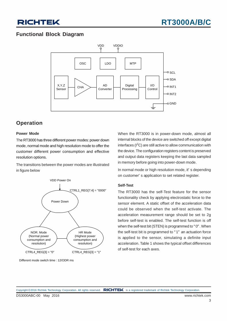
Functional Block Diagram
Digital Processing
OSC
AD Converter
X,Y,Z Sensor
VDD
CHA
GND
SCL
SDA
MTPLDO
I/O Control
VDDIO
INT1
INT2
Operation
Power Mode
The RT3000 has three different power modes: power down
mode, normal mode and high resolution mode to offer the
customer different power consumption and effective
resolution options.
The transitions between the power modes are illustrated
in figure below
When the RT3000 is in power-down mode, almost all
internal blocks of the device are switched off except digital
interfaces (I2C) are still active to allow communication with
the device. The configuration registers content is preserved
and output data registers keeping the last data sampled
in memory before going into power-down mode.
In normal mode or high resolution mode, it’ s depending
on customer’ s application to set related register.
Self-Test
The RT3000 has the self-Test feature for the sensor
functionality check by applying electrostatic force to the
sensor element. A static offset of the acceleration data
could be observed when the self-test activate. The
acceleration measurement range should be set to 2g
before self-test is enabled. The self-test function is off
when the self-test bit (STEN) is programmed to “0”. When
the self-test bit is programmed to “1” an actuation force
is applied to the sensor, simulating a definite input
acceleration. Table 1 shows the typical offset differences
of self-test for each axes.
Power Down
VDD Power On
NOR. Mode (Normal power
consumption and resolution)
HR Mode (Highest power
consumption and resolution)
CTRL4_REG[3] = "1"CTRL4_REG[3] = "0"
CTRL1_REG[7:4] = "0000"
Different mode switch time : 12/ODR ms

RT3000A/B/C
4
DS3000ABC-00 May 2016www.richtek.com
©Copyright 2016 Richtek Technology Corporation. All rights reserved. is a registered trademark of Richtek Technology Corporation.
Table 1. Typical Self-test offset difference values
X-Axis Y-Axis Z-Axis
Offset Difference
80mg 80mg 80mg
FIFO
The RT3000 included an integrated 32 frame FIFO for each
axis. The FIFO which can be configured to operate in
following mode
FIFO Mode
In FIFO mode the acceleration data of selected axis are
stored in the buffer until full. When the buffer is full, the
data collection is stopped. Once the buffer is full; a FIFO-
full interrupt is generated if it has been enabled.
Stream Mode
In stream mode the acceleration data of selected axis are
stored in the buffer until full. When the buffer is full, the
data continues and oldest entry is discarded.
Bypass Mode
In bypass mode, only the current sensor data can be read
out from the FIFO. The FIFO behaves like the stream mode
with a depth of one, compared to reading the data from
normal data register.
Trigger Mode
In trigger mode is a combination of the stream and FIFO
modes described above. In this mode, the FIFO buffer
starts operating in stream mode and switches to FIFO
mode when the selected interrupt occurs.
Start Up and Read Data Sequence
After VDD Power Up 32ms
Power Down Mode
Set ODR Rate : CTRL1_REG[7:4]
Set operation mode : CTRL4_REG[3]
Read STS_REG
ZYXDA = '1'
Read Xdata_L/Xdata_HRead Ydata_L/Ydata_HRead Zdata_L/Zdata_H
Data Processing
No
RT3000A/B/C
5
DS3000ABC-00 May 2016 www.richtek.com
©Copyright 2016 Richtek Technology Corporation. All rights reserved. is a registered trademark of Richtek Technology Corporation.
Recommended Operating Conditions (Note 3)
Input Voltage Range ----------------------------------------------------------------------------------------- 2V to 3.6V
Ambient Temperature Range------------------------------------------------------------------------------- −40°C to 85°C
Mechanical Characteristics
Parameter Symbol Conditions Min Typ Max Unit
Acceleration Range
FS2g
Customer programmable via serial digital interface
-- 2 -- g
FS4g -- 4 -- g
FS8g -- 8 -- g
FS16g -- 16 -- g
Sensitivity
S2g FS2g -- 16384 -- LSB/g
S4g FS4g -- 8192 -- LSB/g
S8g FS8g -- 4096 -- LSB/g
S16g FS16g -- 2048 -- LSB/g
Zero-g Offset Offset2g FS2g -- 45 -- mg
Zero-g Offset Temperature Shift
TCO2g FS2g, 40°C TA 85°C -- 1 -- mg/C
Sensitivity Temperature Shift
TCS2g FS2g, 40°C TA 85°C -- 0.05 -- %/C
Nonlinearity NL Max. deviation to best fit straight line
-- 0.5 -- %FS
Noise Nrms FS2g -- 3 -- mg
Cross Axis Sensitivity CAS Relative contribution from the other to axes
-- 1.25 -- %
(VDD = 2.5V, TA = 25°C unless otherwise specified)
Absolute Maximum Ratings (Note 1)
VDD Supply Voltage ----------------------------------------------------------------------------------------- −0.2V to 4V
VDDIO Supply Voltage -------------------------------------------------------------------------------------- −0.2V to 4V
SCL, SDA, INT1, INT2 -------------------------------------------------------------------------------------- −0.2V to (VDDIO + 0.3V)
Storage Temperature Range ------------------------------------------------------------------------------- −40°C to 125°C ESD Susceptibility (Note 2)
HBM (Human Body Model) --------------------------------------------------------------------------------- 2kV
CDM (Charged Device Model) ----------------------------------------------------------------------------- 1kV
Mechanical Shock (Unpowered) -------------------------------------------------------------------------- 10000g for 0.2ms
Electrical Characteristics(VDD = 2.5V, TA
= 25°C unless otherwise specified)
Parameter Symbol Conditions Min Typ Max Unit
Supply Voltage - Core VDD 2 2.5 3.6 V
Supply Voltage – I/O VDDIO 1.5 2.5 3.6 V
Input Voltage Low VIL I2C -- -- 0.3
VDDIO V
Input Voltage High VIH I2C 0.7
VDDIO -- -- V

RT3000A/B/C
6
DS3000ABC-00 May 2016www.richtek.com
©Copyright 2016 Richtek Technology Corporation. All rights reserved. is a registered trademark of Richtek Technology Corporation.
Electrical Characteristics : I2C Interface
Parameter Symbol Standard mode Fast mode
Unit Min Max Min Max
SCL Clock Frequency fSCLK 10 100 10 400 kHz
Hold Time After (Repeated) Start Condition. After This Period, The First Clock Is Generated
tHDSTA 4 -- 0.6 -- s
LOW Period Of The SCL Clock tLOW 4.7 -- 1.3 -- s
HIGH Period Of The SCL Clock tHIGH 4.0 -- 0.6 -- s
Set-Up Time For A Repeated START Condition
tSUSTA 4.7 -- 0.6 -- s
Data Hold Time tHDDAT -- 120 -- 120 ns
tSUDAT Data Set-Up Time tSUDAT 250 -- 100 ns
Rise Time Of Both SDA And SCL Signals tr -- 1000 -- 300 ns
Fall Time Of Both SDA And SCL Signals tf -- 300 -- 300 ns
Set-Up Time For STOP Condition tSUSTO 4.0 -- 0.6 -- s
Bus Free Time Between A STOP And START Condition
4.7 -- 1.3 -- s
Parameter Symbol Conditions Min Typ Max Unit
Output Voltage Low VOL -- -- 0.2
VDDIO V
Output Voltage High VOH 0.8
VDDIO -- -- V
Current Consumption @ Normal Mode
IDDN ODR = 200Hz -- 120 -- A
Current Consumption @ Normal Mode
IDDN ODR = 25Hz -- 15 -- A
Current Consumption @ Power Down Mode
IDDS -- 1 -- A
Wake-Up Time tWU
Time from power down mode to normal mode or high resolution mode
-- 1.8 -- ms
Start-Up Time tSU Time for power on reset. -- 40 -- ms
Note 1. Stresses beyond those listed “Absolute Maximum Ratings” may cause permanent damage to the device. These are
stress ratings only, and functional operation of the device at these or any other conditions beyond those indicated in
the operational sections of the specifications is not implied. Exposure to absolute maximum rating conditions may
affect device reliability.
Note 2. Devices are ESD sensitive. Handling precaution is recommended.
Note 3. The device is not guaranteed to function outside its operating conditions.

RT3000A/B/C
7
DS3000ABC-00 May 2016 www.richtek.com
©Copyright 2016 Richtek Technology Corporation. All rights reserved. is a registered trademark of Richtek Technology Corporation.
Figure 1. Timing Chart of the I2C
Figure 2. Write Command
Figure 3. Read Data
VIH
VIL
tf
tLOW
tHDSTA
tSCLK
tHDDAT
tSUDAT
tHIGH
tSUSTA tHDSTA tSUSTO
tBUF
tr
START START STOP
SDA
SCL
WR ACKDevice Address Register Address Write DataACK ACK
START STOP
SDA
SCL
WR ACKDevice Address Register Address
START STOP
SDA
SCL
RD ACKDevice Address Read Data
START STOP
ACK
NAK

RT3000A/B/C
8
DS3000ABC-00 May 2016www.richtek.com
©Copyright 2016 Richtek Technology Corporation. All rights reserved. is a registered trademark of Richtek Technology Corporation.
Typical Application Circuit
RT3000B (MQFN-12L 2x2)
RT3000C (MDFN-10L 3x3)
RT3000A (MQFN-16L 3x3)
1
2
3
4
10
9
8
7
12 11
5 6
SDA
10k
SCLVDDIO
0.1µF
INT1 INT2
VDD
10k
0.1µF
1
2
3
4
5
10
9
8
7
611
0.1µFVDD
INT1
VDDIO
SDA
SCL
10k10k0.1µF
VDDIO
SCL
SDA
INT2
INT1
VDD
0.1µF
0.1µF10k10k
17
1
2
3
4
5
13
12
11
10
9
16 15 14
6 7 8

RT3000A/B/C
9
DS3000ABC-00 May 2016 www.richtek.com
©Copyright 2016 Richtek Technology Corporation. All rights reserved. is a registered trademark of Richtek Technology Corporation.
Register MapRegister
Address Type Name
Default
Value Bit-7 Bit-6 Bit-5 Bit-4 Bit-3 Bit-2 Bit-1 Bit-0
0x06 R/W CTRL_REG0 0000 0000 0 0 LIR_CLICK -- 0 INAEN CLICKEN AOIEN
0x0F R WHO_AM_I 0011 0011 0 0 1 1 0 0 1 1
0x20 R/W CTRL_REG1 0000 0111 ODR3 ODR2 ODDR1 ODR0 0 ZEN YEN XEN
0x21 R/W CTRL_REG2 0000 0000 -- -- HPCF2 HPCF1 FDOUT HPCLICK -- HPIS1
0x22 R/W CTRL_REG3 0000 0000 I1_CLICK I1_AOI I1_INACT I1_DRDY1 -- I1_WTM I1_ORUN --
0x23 R/W CTRL_REG4 0000 0000 BDU BIGEN FS1 FS0 HR -- STEN --
0x24 R/W CTRL_REG5 0000 0000 BOOT FIFOEN 0 0 LIR_AOI ODS_AOI -- --
0x25 R/W CTRL_REG6 0000 0000 I2_CLICK_EN I2_AOI -- I2_BOOT -- -- HL_ACTIVE --
0x27 R STS_REG -- ZYXOVER ZOVER YOVER XOVER ZYXDA ZDA YDA XDA
0x28 R OUT_X_L Output XD7 XD6 XD5 XD4 XD3 XD2 XD1 XD0
0x29 R OUT_X_H Output XD15 XD14 XD13 XD12 XD11 XD10 XD9 XD8
0x2A R OUT_Y_L Output YD7 YD6 YD5 YD4 YD3 YD2 YD1 YD0
0x2B R OUT_Y_H Output YD15 YD14 YD13 YD12 YD11 YD10 YD9 YD8
0x2C R OUT_Z_L Output ZD7 ZD6 ZD5 ZD4 ZD3 ZD2 ZD1 ZD0
0x2D R OUT_Z_H Output ZD15 ZD14 ZD13 ZD12 ZD11 ZD10 ZD9 ZD8
0x2E R/W FIFO_CFG 0000 0000 FM1 FM0 TR FTH4 FTH3 FTH2 FTH1 FTH0
0x2F R FIFO_SRC -- WTM OVRN_
FIFO EMPTY FSS4 FSS3 FSS2 FSS1 FSS0
0x30 R/W AOI_CFG 0000 0000 AOI1 AOI0 ZHIE/
ZUPE1
ZLIE/
ZDOWNE1
YHIE/
YUPE1
YLIE/
YDOWNE1
XHIE/
XUPE1
XLIE/
XDOWNE1
0x31 R AOI_SRC -- -- IA1 ZH1 ZL1 YH1 YL1 XH1 XL1
0x32 R/W AOI_THS 0000 0000 -- AOIH6 AOIH5 AOIH4 AOIH3 AOIH2 AOIH1 AOIH0
0x33 R/W AOI_DUR 0000 0000 -- AOID6 AOID5 AOID4 AOID3 AOID2 AOID1 AOID0
0x38 R/W CLICK_CFG 0000 0000 -- -- ZDEN ZSEN YDEN YSEN XDEN XSEN
0x39 R CLICK_SRC -- -- IA DCLICK SCLICK CLICK_SIGN ZCLICK YCLICK XCLICK
0x3A R/W CLICK_THS 0000 0000 -- CTHS6 CTHS5 CTHS4 CTHS3 CTHS2 CTHS1 CTHS0
0x3B R/W TIME_LIMIT 0000 0000 -- TLI6 TLI5 TLI4 TLI3 TLI2 TLI1 TLI0
0x3C R/W TIME_LATENCY 0000 0000 TLA7 TLA6 TLA5 TLA4 TLA3 TLA2 TLA1 TLA0
0x3D R/W TIME_WINDOW 0000 0000 TW7 TW6 TW5 TW4 TW3 TW2 TW1 TW0
0x3E R/W INACT_THS 0000 0000 INACT_STS INAH6 INAH5 INAH4 INAH3 INAH2 INAH1 INAH0
0x3F R/W INACT_DUR 0000 0000 INAD7 INAD6 INAD5 INAD4 INAD3 INAD2 INAD1 INAD0

RT3000A/B/C
10
DS3000ABC-00 May 2016www.richtek.com
©Copyright 2016 Richtek Technology Corporation. All rights reserved. is a registered trademark of Richtek Technology Corporation.
Register 0x06 (CTRL_REG0)
Bit-7 Bit-6 Bit-5 Bit-4 Bit-3 Bit-2 Bit-1 Bit-0
0 0 LIR_CLICK 0 0 INAEN CLICKEN AOIEN
Bit Type Name Default Description
5 R/W LIR_CLICK 0 Latch click event interrupt. 0 : disable; 1 : enable
2 R/W INAEN 0 Inactivity detection. 0 : disable; 1 : enable
1 R/W CLICKEN 0 Click detection. 0 : disable; 1 : enable
0 R/W AOIEN 0 AOIEN detection. 0 : disable; 1 : enable
Register 0x0F (WHO_AM_I)
Bit-7 Bit-6 Bit-5 Bit-4 Bit-3 Bit-2 Bit-1 Bit-0
0 0 1 1 0 0 1 1
Bit Type Name Default Description
[7:0] R ID7:ID0 00110011 Device ID
Register 0x20 (CTRL_REG1)
Bit-7 Bit-6 Bit-5 Bit-4 Bit-3 Bit-2 Bit-1 Bit-0
ODR3 ODR2 ODR1 ODR0 0 ZEN YEN XEN
Bit Type Name Default Description
[7:4] R/W ODR3:ODR0 0000
Data rate selection. 0000 : Power down mode 0001 : 1Hz 0010 : 10Hz 0011 : 25Hz 0100 : 50Hz 0101 : 100Hz 0110 : 200Hz
2 R/W ZEN 1 Z axis enable. 0 : disable; 1 : enable
1 R/W YEN 1 Y axis enable. 0 : disable; 1 : enable
0 R/W XEN 1 X axis enable. 0 : disable; 1 : enable
Register Table Lists (I2C slave address : 19h)

RT3000A/B/C
11
DS3000ABC-00 May 2016 www.richtek.com
©Copyright 2016 Richtek Technology Corporation. All rights reserved. is a registered trademark of Richtek Technology Corporation.
Register 0x21 (CTRL_REG2)
Bit-7 Bit-6 Bit-5 Bit-4 Bit-3 Bit-2 Bit-1 Bit-0
0 0 HPCF2 HPCF1 FDOUT HPCLICK 0 HPIS1
Bit Type Name Default Description
[5:4] R/W HPCF2 : HPCF1 00
High pass filter cut off frequency selection. 00 : ODR/12.5 01 : ODR/25 10 : ODR/50 11 : ODR/75
3 R/W FDOUT 0 Filtered data selection. 0: high pass filter bypassed; 1: data from high pass filter sent to output register and FIFO
2 RW HPCLICK 0 High pass filter enabled for CLICK function. 0 : disable; 1 : enable
0 R/W HPIS1 0 High pass filter enabled for AOI function. 0: disable; 1 : enable
Register 0x22 (CTRL_REG3)
Bit-7 Bit-6 Bit-5 Bit-4 Bit-3 Bit-2 Bit-1 Bit-0
I1_CLICK I1_AOI I1_INACT I1_DRDY1 0 I1_WTM I1_ORUN 0
Bit Type Name Default Description
7 R/W I1_CLICK 0 Click interrupt on INT1. 0 : disable; 1 : enable
6 R/W I1_AOI 0 AOI interrupt on INT1. 0 : disable; 1 : enable
5 R/W I1_INACT 0 Inactivity interrupt on INT1. 0 : disable; 1 : enable
4 R/W I1_DRDY1 0 Data-ready interrupt on INT1. 0 : disable; 1 : enable
2 R/W I1_WTM 0 FIFO watermark interrupt on INT1. 0 : disable; 1 : enable
1 R/W I1_ORUN 0 FIFO overrun interrupt on INT1. 0 : disable; 1 : enable
Register 0x23 (CTRL_REG4)
Bit-7 Bit-6 Bit-5 Bit-4 Bit-3 Bit-2 Bit-1 Bit-0
BDU BIGEN FS1 FS0 HR 0 STEN 0
Bit Type Name Default Description
7 R/W BDU 0 Block data update. 0: disable; 1: enable
6 R/W BIGEN 0 Big endian enable. 0: Data LSB @ lower address. 1 : Data MSB @ lower address
[5:4] R FS1:FS0 00 Full scale range selection. 00 : 2G; 01 : 4G; 10 : 8G; 11 : 16G
3 R/W HR 0 High resolution mode. 0 : disable; 1 : enable
1 R/W STEN 0 Self-test mode. 0 : disable; 1 : enable
RT3000A/B/C
12
DS3000ABC-00 May 2016www.richtek.com
©Copyright 2016 Richtek Technology Corporation. All rights reserved. is a registered trademark of Richtek Technology Corporation.
Register 0x24 (CTRL_REG5)
Bit-7 Bit-6 Bit-5 Bit-4 Bit-3 Bit-2 Bit-1 Bit-0
BOOT FIFOEN 0 0 LIR_AOI ODS_AOI 0 0
Bit Type Name Default Description
7 R/W BOOT 0 Reboot. 0: disable; 1 : enable
6 R/W FIFOEN 0 FIFO enable. 0 : disable; 1 : enable
3 R/W LIR_AOI 0 Latch AOI event interrupt. 0 : disable; 1 : enable
2 R/W ODS_AOI 0 Orientation detection selection. 0: 6D orientation; 1: 4D orientation
Register 0x25 (CTRL_REG6)
Bit-7 Bit-6 Bit-5 Bit-4 Bit-3 Bit-2 Bit-1 Bit-0
I2_CLICK_EN I2_AOI 0 I2_BOOT 0 0 HL_ACTIVE 0
Bit Type Name Default Description
7 R/W I2_CLICK_EN 0 Click interrupt on INT2 pin. 0 : disable; 1 : enable
6 R/W I2_AOI 0 AOI interrupt on INT2 pin. 0 : disable; 1 : enable
4 R/W I2_BOOT 0 Boot status on INT2 pin. 0 : disable; 1 : enable
1 R/W HL_ACTIVE 0 Active high/low level for interrupt pins. 0: active high; 1: active low
Register 0x27 (STS_REG)
Bit-7 Bit-6 Bit-5 Bit-4 Bit-3 Bit-2 Bit-1 Bit-0
ZYXOVER ZOVER YOVER XOVER ZYXDA ZDA YDA XDA
Bit Type Name Default Description
7 R ZYXOVER 0 X, Y and Z axis data overrun. 0 : normal; 1: overrun
6 R ZOVER 0 Z axis data overrun. 0: normal; 1 : overrun
5 R YOVER 0 Y axis data overrun. 0: normal; 1 : overrun
4 R XOVER 0 X axis data overrun. 0: normal; 1 : overrun
3 R ZYXDA 0 X, Y and Z axis new data available. 0 : not available; 1 : available
2 R ZDA 0 Z axis new data available. 0 : not available; 1 : available
1 R YDA 0 Y axis new data available. 0 : not available; 1 : available
0 R XDA 0 X axis new data available. 0 : not available; 1 : available

RT3000A/B/C
13
DS3000ABC-00 May 2016 www.richtek.com
©Copyright 2016 Richtek Technology Corporation. All rights reserved. is a registered trademark of Richtek Technology Corporation.
Register 0x28 (OUT_X_L)
Bit-7 Bit-6 Bit-5 Bit-4 Bit-3 Bit-2 Bit-1 Bit-0
XD7 XD6 XD5 XD4 XD3 XD2 XD1 XD0
Bit Type Name Default Description
[7:0] R XD7:XD0 00000000 Low byte of X axis data.
Register 0x29 (OUT_X_H)
Bit-7 Bit-6 Bit-5 Bit-4 Bit-3 Bit-2 Bit-1 Bit-0
XD15 XD14 XD13 XD12 XD11 XD10 XD9 XD8
Bit Type Name Default Description
[7:0] R XD15:XD8 00000000 High byte of X axis data.
Register 0x2A (OUT_Y_L)
Bit-7 Bit-6 Bit-5 Bit-4 Bit-3 Bit-2 Bit-1 Bit-0
YD7 YD6 YD5 YD4 YD3 YD2 YD1 YD0
Bit Type Name Default Description
[7:0] R YD7:YD0 00000000 Low byte of Y axis data.
Register 0x2B (OUT_Y_H)
Bit-7 Bit-6 Bit-5 Bit-4 Bit-3 Bit-2 Bit-1 Bit-0
YD15 YD14 YD13 YD12 YD11 YD10 YD9 YD8
Bit Type Name Default Description
[7:0] R YD15:YD8 00000000 High byte of Y axis data.
Register 0x2C (OUT_Z_L)
Bit-7 Bit-6 Bit-5 Bit-4 Bit-3 Bit-2 Bit-1 Bit-0
ZD7 ZD6 ZD5 ZD4 ZD3 ZD2 ZD1 ZD0
Bit Type Name Default Description
[7:0] R ZD7:ZD0 0 Low byte of Z axis data.
Register 0x2D (OUT_Z_H)
Bit-7 Bit-6 Bit-5 Bit-4 Bit-3 Bit-2 Bit-1 Bit-0
ZD15 ZD14 ZD13 ZD12 ZD11 ZD10 ZD9 ZD8
Bit Type Name Default Description
[7:0] R ZD15:ZD8 0 High byte of Z axis data.

RT3000A/B/C
14
DS3000ABC-00 May 2016www.richtek.com
©Copyright 2016 Richtek Technology Corporation. All rights reserved. is a registered trademark of Richtek Technology Corporation.
Register 0x2E (FIFO_CFG)
Bit-7 Bit-6 Bit-5 Bit-4 Bit-3 Bit-2 Bit-1 Bit-0
FM1 FM0 TR FTH4 FTH3 FTH2 FTH1 FTH0
Bit Type Name Default Description
[7:6] R/W FM1:FM0 00
FIFO mode selection. 00 : Bypass mode 01 : FIFO mode 10 : Stream mode 11 : Trigger mode
5 R/W TR 0 Trigger selection. 0 : Trigger event liked to trigger signal on AOI 1 : Trigger event liked to trigger signal on CLICK
[4:0] R/W FTH4:FTH0 00000 FTH[4:0] bits are intended to define the watermark level. When FIFO content exceeds this value, the WTM flag is set to “1” in the FIFO_SRC register.
Register 0x2F (FIFO_SRC)
Bit-7 Bit-6 Bit-5 Bit-4 Bit-3 Bit-2 Bit-1 Bit-0
WTM OVRN_FIFO EMPTY FSS4 FSS3 FSS2 FSS1 FSS0
Bit Type Name Default Description
7 R WTM 0 WTM flag is set high when FIFO content exceeds watermark level.
6 R OVRN_FIFO 0 OVRN flag is set high when FIFO buffer is full, this means that the FIFO buffer contains 32 unread samples.
5 R EMPTY 0 EMPTY flag is set high when all FIFO samples have been read and FIFO is empty.
[4:0] R FSS4:FSS0 00000 FSS[4:0] field always contains the current number of unread samples stored in the FIFO buffer.

RT3000A/B/C
15
DS3000ABC-00 May 2016 www.richtek.com
©Copyright 2016 Richtek Technology Corporation. All rights reserved. is a registered trademark of Richtek Technology Corporation.
Register 0x30 (AOI_CFG)
Bit-7 Bit-6 Bit-5 Bit-4 Bit-3 Bit-2 Bit-1 Bit-0
AOI1 AOI0 ZHIE/
ZUPE1 ZLIE /
ZDOWNE1 YHIE / YUPE1
YLIE / YDOWNE1
XHIE / XUPE1
XLIE / XDOWNE1
Bit Type Name Default Description
[7:6] R/W AOI1:AOI0 00
Motion detection mode selection. 00 : wakeup 01 : 6D/4D movement 10 : free-fall 11 : 6D/4D position
5 R/W ZHIE/ZUPE1 0 Z-axis high-g interrupt generation for AOI function. 0: disable; 1: enable
4 R/W ZLIE/ZDOWNE1 0 Z-axis low-g interrupt generation for AOI function. 0: disable; 1: enable
3 R/W YHIE/YUPE1 0 Y-axis high-g interrupt generation for AOI function. 0: disable; 1: enable
2 R/W YLIE/YDOWNE1 0 Y-axis low-g interrupt generation for AOI function. 0: disable; 1: enable
1 R/W XHIE/XUPE1 0 X-axis high-g interrupt generation for AOI function. 0: disable; 1: enable
0 R/W XLIE/XDOWNE1 0 X-axis low-g interrupt generation for AOI function. 0: disable; 1: enable
Register 0x31 (AOI_SRC)
Bit-7 Bit-6 Bit-5 Bit-4 Bit-3 Bit-2 Bit-1 Bit-0
0 IA1 ZH1 ZL1 YH1 YL1 XH1 XL1
Bit Type Name Default Description
6 R IA1 0 AOI status. 0: no event; 1: one or more events have been generated
5 R ZH1 0 Z-axis high-g event status for AOI function. 0: inactive; 1: active
4 R ZL1 0 Z-axis low-g event status for AOI function. 0: inactive; 1: active
3 R YH1 0 Y-axis high-g event status for AOI function. 0: inactive; 1: active
2 R YL1 0 Y-axis low-g event status for AOI function. 0: inactive; 1: active
1 R XH1 0 X-axis high-g event status for AOI function. 0: inactive; 1: active
0 R XL1 0 X-axis low-g event status for AOI function. 0: inactive; 1: active

RT3000A/B/C
16
DS3000ABC-00 May 2016www.richtek.com
©Copyright 2016 Richtek Technology Corporation. All rights reserved. is a registered trademark of Richtek Technology Corporation.
Register 0x32 (AOI_THS)
Bit-7 Bit-6 Bit-5 Bit-4 Bit-3 Bit-2 Bit-1 Bit-0
0 AOIH6 AOIH5 AOIH 4 AOIH3 AOIH2 AOIH1 AOIH0
Bit Type Name Default Description
[6:0] R/W AOIH6:AOIH0 0000000 AOI threshold.
Register 0x33 (AOI_DUR)
Bit-7 Bit-6 Bit-5 Bit-4 Bit-3 Bit-2 Bit-1 Bit-0
0 AOID6 AOID5 AOID4 AOID3 AOID2 AOID1 AOID0
Bit Type Name Default Description
[6:0] R/W AOID6:AOID0 0000000 AOI duration. Unit: 1/ODR
Register 0x38 (CLICK_CFG)
Bit-7 Bit-6 Bit-5 Bit-4 Bit-3 Bit-2 Bit-1 Bit-0
0 0 ZDEN ZSEN YDEN YSEN XDEN XSEN
Bit Type Name Default Description
5 R/W ZDEN 0 Double click detection on z-axis. 0 : disable; 1 : enable
4 R/W ZSEN 0 Single click detection on z-axis. 0 : disable; 1 : enable
3 R/W YDEN 0 Double click detection on y-axis. 0 : disable; 1 : enable
2 R/W YSEN 0 Single click detection on y-axis. 0 : disable; 1 : enable
1 R/W XDEN 0 Double click detection on x-axis. 0 : disable; 1 : enable
0 R/W XSEN 0 Single click detection on x-axis. 0 : disable; 1 : enable

RT3000A/B/C
17
DS3000ABC-00 May 2016 www.richtek.com
©Copyright 2016 Richtek Technology Corporation. All rights reserved. is a registered trademark of Richtek Technology Corporation.
Register 0x39 (CLICK_SRC)
Bit-7 Bit-6 Bit-5 Bit-4 Bit-3 Bit-2 Bit-1 Bit-0
0 IA DCLICK SCLICK CLICK_SIGN ZCLICK YCLICK XCLICK
Bit Type Name Default Description
6 R IA 0 Click interrupt status. 0 : inactive; 1 : active
5 R DCLICK 0 Double-click interrupt status. 0 : inactive; 1 : active
4 R SCLICK 0 Single-click interrupt status. 0 : inactive; 1 : active
3 R CLICK_SIGN 0 Sign of click event status. 0 : positive; 1 : negative
2 R ZCLICK 0 Click event detection status on z-axis. 0 : not detected; 1 : detected
1 R YCLICK 0 Click event detection status on y-axis. 0 : not detected; 1 : detected
0 R XCLICK 0 Click event detection status on x-axis. 0 : not detected; 1 : detected
Register 0x3A (CLICK_THS)
Bit-7 Bit-6 Bit-5 Bit-4 Bit-3 Bit-2 Bit-1 Bit-0
0 CTHS6 CTHS5 CTHS4 CTHS3 CTHS2 CTHS1 CTHS0
Bit Type Name Default Description
[6:0] R/W CTHS6: CTHS0 0000000 Click threshold.
Register 0x3B (TIME_LIMIT)
Bit-7 Bit-6 Bit-5 Bit-4 Bit-3 Bit-2 Bit-1 Bit-0
0 TLI6 TLI5 TLI4 TLI3 TLI2 TLI1 TLI0
Bit Type Name Default Description
[6:0] R/W TLI6: TLI0 0000000 Click time limit. Unit : 1/ODR
Register 0x3C (TIME_LATENCY)
Bit-7 Bit-6 Bit-5 Bit-4 Bit-3 Bit-2 Bit-1 Bit-0
TLA7 TLA6 TLA5 TLA4 TLA3 TLA2 TLA1 TLA0
Bit Type Name Default Description
[7:0] R/W TLA7: TLA0 00000000 Click time latency. Unit : 1/ODR
Register 0x3D (TIME_WINDOW)
Bit-7 Bit-6 Bit-5 Bit-4 Bit-3 Bit-2 Bit-1 Bit-0
TW7 TW6 TW5 TW4 TW3 TW2 TW1 TW0
Bit Type Name Default Description
[7:0] R/W TW7: TW0 00000000 Click time window. Unit: 1/ODR

RT3000A/B/C
18
DS3000ABC-00 May 2016www.richtek.com
©Copyright 2016 Richtek Technology Corporation. All rights reserved. is a registered trademark of Richtek Technology Corporation.
Register 0x3E (INACT_THS)
Bit-7 Bit-6 Bit-5 Bit-4 Bit-3 Bit-2 Bit-1 Bit-0
INACT_STS INAH6 INAH5 INAH4 INAH3 INAH2 INAH1 INAH0
Bit Type Name Default Description
7 R INACT_STS 0 Inactivity interrupt status. 0 : inactive; 1 : active
[6:0] R/W INAH6 : INAH0 0000000 Inactivity threshold.
Register 0x3F (INACT_DUR)
Bit-7 Bit-6 Bit-5 Bit-4 Bit-3 Bit-2 Bit-1 Bit-0
INAD7 INAD6 INAD5 INAD4 INAD3 INAD2 INAD1 INAD0
Bit Type Name Default Description
[7:0] R/W INAD7 : INAD0 00000000 Inactivity duration. Unit: 16/ODR
Sensing Axes Orientation
The sensor is at rest in gravity filed according to following figure, and the output signals are :
0g for the X-axis
0g for the Y-axis
+1g for the Z-axis
MDFN-10L 3x3MQFN-16L 3x3
Gravity
Y
Z
X
Gravity
X
Z
Y
Gravity
Y
Z
X
MQFN-12L 2x2 (COL)

RT3000A/B/C
19
DS3000ABC-00 May 2016 www.richtek.com
©Copyright 2016 Richtek Technology Corporation. All rights reserved. is a registered trademark of Richtek Technology Corporation.
Soldering Guidelines
Condition Contents
Preheat temperature 175 (25)C 60 to 180 seconds
Temperature maintained above 217C 60 to 150 seconds
Time within 5C of actual peak temperature 20 to 40 seconds
Peak temperature 260C
Ramp-down rate 6C /second max.
Time 25C to peak temperature 8 minutes max.
Layout Considerations
No extra traces and components under the device.
Do not place any components or vias at a distance less than 2 mm from the device.
The solder mask opening must be larger than the land pad.
Use a pick and place machine and the solder paste thickness must be as uniform as possible to avoid uneven stress.

RT3000A/B/C
20
DS3000ABC-00 May 2016www.richtek.com
©Copyright 2016 Richtek Technology Corporation. All rights reserved. is a registered trademark of Richtek Technology Corporation.
Recommended Land Pattern
RT3000B (MQFN-12L 2x2)
RT3000C (MDFN-10L 3x3)
1
1
RT3000A (MQFN-16L 3x3)
1

RT3000A/B/C
21
DS3000ABC-00 May 2016 www.richtek.com
©Copyright 2016 Richtek Technology Corporation. All rights reserved. is a registered trademark of Richtek Technology Corporation.
Outline Dimension
M-Type 16L QFN 3x3 Package
Symbol Dimensions In Millimeters Dimensions In Inches
Min. Max. Min. Max.
A 0.900 1.000 0.035 0.039
A1 0.000 0.050 0.000 0.002
A3 0.175 0.250 0.007 0.010
b 0.200 0.300 0.008 0.012
D 2.900 3.100 0.114 0.122
D2 1.250 1.350 0.049 0.053
E 2.900 3.100 0.114 0.122
E2 1.250 1.350 0.049 0.053
e 0.500 0.020
L 0.300 0.400 0.012 0.016
L1 0.400 0.500 0.016 0.020
K 0.050 0.150 0.002 0.006

©Copyright 2016 Richtek Technology Corporation. All rights reserved. is a registered trademark of Richtek Technology Corporation.
RT3000A/B/C
22
DS3000ABC-00 May 2016www.richtek.com
M-Type 12L QFN 2x2 (COL) Package
Symbol Dimensions In Millimeters Dimensions In Inches
Min. Max. Min. Max.
A 0.900 1.000 0.035 0.039
A1 0.000 0.050 0.000 0.002
A3 0.175 0.250 0.007 0.010
b 0.200 0.300 0.008 0.012
D 1.900 2.100 0.075 0.083
E 1.900 2.100 0.075 0.083
e 0.500 0.020
L 0.250 0.350 0.010 0.014
L1 0.325 0.425 0.013 0.017
K 0.025 0.125 0.001 0.005

RT3000A/B/C
23
DS3000ABC-00 May 2016 www.richtek.com
Richtek Technology Corporation14F, No. 8, Tai Yuen 1st Street, Chupei City
Hsinchu, Taiwan, R.O.C.
Tel: (8863)5526789
Richtek products are sold by description only. Richtek reserves the right to change the circuitry and/or specifications without notice at any time. Customers should
obtain the latest relevant information and data sheets before placing orders and should verify that such information is current and complete. Richtek cannot
assume responsibility for use of any circuitry other than circuitry entirely embodied in a Richtek product. Information furnished by Richtek is believed to be
accurate and reliable. However, no responsibility is assumed by Richtek or its subsidiaries for its use; nor for any infringements of patents or other rights of third
parties which may result from its use. No license is granted by implication or otherwise under any patent or patent rights of Richtek or its subsidiaries.
M-Type 10L DFN 3x3 Package
Min. Max. Min. Max.
A 0.900 1.000 0.035 0.039
A1 0.000 0.050 0.000 0.002
A3 0.175 0.250 0.007 0.010
b 0.200 0.300 0.008 0.012
D 2.950 3.050 0.116 0.120
D2 2.150 2.250 0.085 0.089
E 2.950 3.050 0.116 0.120
E2 0.950 1.050 0.037 0.041
e
L 0.300 0.400 0.012 0.016
L1 0.400 0.500 0.016 0.020
K 0.050 0.150 0.002 0.006
SymbolDimensions In Millimeters Dimensions In Inches
0.500 0.020