2D-1D Semiconductor ... - Department of Physics Projects Repository... · 2D-1D Semiconductor...
52
2D-1D Semiconductor Heterostructures: Synthesis, Characterisation and Optoelectronic Applications ANG JIAN MARTIN A0087255X A THESIS SUBMITTED FOR THE FULFILLMENT FOR THE DEGREE IN BACHELOR OF SCIENCE (HONOURS) DEPARTMENT OF PHYSICS NATIONAL UNIVERSITY OF SINGAPORE AY2014/15
Transcript of 2D-1D Semiconductor ... - Department of Physics Projects Repository... · 2D-1D Semiconductor...
2D-1D Semiconductor Heterostructures:
Synthesis, Characterisation and Optoelectronic
Applications
ANG JIAN MARTIN
A0087255X
A THESIS SUBMITTED FOR THE FULFILLMENT FOR THE DEGREE IN
BACHELOR OF SCIENCE (HONOURS)
DEPARTMENT OF PHYSICS
NATIONAL UNIVERSITY OF SINGAPORE
AY2014/15

Acknowledgements
This Final Year Project is indeed an experience to remember. This journey had its
excitements and disappointments. It has given me a glimpse into the life of a researcher,
experiencing both the frustration that come with setbacks, and the joy that come from
breakthroughs. There are many people along the way who have given me invaluable help and
support. Without them, doing this project would be become exponentially tougher.
First of all, I would like to thank my supervisor, Professor Sow Chorng Haur, for all his
guidance through my project. Being the Head of Department for Physics, he was always very
busy. However, he always managed to make time to drop by and ask us how we were and
how our projects were doing. He would listen and then guide us to what the next appropriate
cause of action should be. He also had this amazing ability to explain difficult concepts in a
surprisingly simple way, which made learning under him a lot easier. This was something I
found very fascinating as I am planning to become a teacher myself. I am very glad to have
had him as my supervisor.
I would also like to thank my mentor, Lu Junpeng, for walking us through this project, taking
the time out to sit down with us each day to check our progress and advising us accordingly. I
am very thankful for him teaching me how to use the equipment in the lab, as well as
explaining concepts to me.
I also would like to thank the others in my lab for being such pleasant people to be with. Not
only are they very friendly to talk to and joke around with every once in a while, but
everybody is also so willing to help each other, be it helping to troubleshoot a problem with
equipment or even just looking for a specific thing in the messy old lab. All this helps in
creating a very warm and welcoming environment at the lab. It was something that I noticed
within the first few weeks of my project, and it is something that I treasure.
Lastly, I would also like to thank my family and friends for supporting me through this time.
Friends were also good to talk to during the struggles with the project as many of them could
empathise with me, especially the other year 4 students. After a day of experiments that gives
you results that just do not make sense to you, and feeling lost, it is always a very comforting
thing to come back to a family that loves you.
Table of Contents
1. Abstract ............................................................................................................................................... 4
2. Introduction ........................................................................................................................................ 5
2.1. Project Description.............................................................................................................. 5
2.2. Transition Metal Dichalcogenides (TMDs) .......................................................................... 6
2.3. Chemical Vapour Deposition (CVD) .................................................................................... 7
2.4. p-n junction ......................................................................................................................... 8
3. Methodology ..................................................................................................................................... 11
3.1. Synthesis of WS2 through Chemical Vapour Deposition (CVD)......................................... 11
3.1.1. Furnace used to synthesize WS2 on SiO2/Si ...................................................... 11
3.1.2. Furnace used to synthesize WS2 on Sapphire ................................................... 13
3.2. Characterisation of WS2 .................................................................................................... 14
3.2.1. Raman Spectroscopy......................................................................................... 14
3.2.2. Photoluminescence Spectroscopy .................................................................... 15
3.2.3. Atomic Force Microscopy (AFM) ...................................................................... 16
3.2.4. Fluorescence Microscopy ................................................................................. 16
3.3. Optoelectronic Device ...................................................................................................... 17
3.3.1. Fabrication of Optoelectronic Device ............................................................... 17
3.3.2. Measuring Photocurrent ................................................................................... 19
4. Results ............................................................................................................................................... 21
4.1. Synthesis of WS2 with CVD ................................................................................................ 21
4.1.1. Synthesis on SiO2/Si substrate .......................................................................... 21
4.1.2. Synthesis on sapphire substrate ....................................................................... 30
4.2. Characterisation of thin WS2 flakes .................................................................................. 35
4.2.1. Raman Spectroscopy......................................................................................... 36
4.2.2. Photoluminescence Spectroscopy .................................................................... 37
4.2.3. Atomic Force Microscopy (AFM) ...................................................................... 38
4.2.4. Fluorescence Microscopy ................................................................................. 40
4.3. Optoelectronic Device ...................................................................................................... 42
4.3.1. IV graphs ........................................................................................................... 43
4.3.2. Current against time (Ivst) graphs .................................................................... 44
5. Conclusion ......................................................................................................................................... 49
5.1. Summary of project .......................................................................................................... 49
5.2. Possible Future Work ........................................................................................................ 49
References: ........................................................................................................................................... 51
1. Abstract
2D materials have become very popular in recent years in the electronics industry. This is due
to the unique properties of a 2D material compared to its bulk form. In my project, Chemical
Vapour Deposition (CVD) is used to fabricate 2D Transition Metal Dichalcogenides (TMDs)
on either a Sapphire or Silicon dioxide (SiO2/Si) substrate. The characteristics of these TMD
flakes are studied through the use of different techniques. Raman Spectroscopy is used to
identify the TMD. Photoluminescence Spectroscopy helps determine its bandgap. Atomic
Force Microscopy allows me to study the morphology of the TMD flake. Fluorescence
Microscopy helps determine the specific areas of fluorescence on the TMD flake. This is
followed by a manual stacking of a Cadmium Selenium Sulfide, CdS0.8Se0.2, nanowire. This
forms a heterostructure junction. This junction is made into an optoelectronic device. Lasers
of different wavelengths were incident upon the junction through global irradiation and the
photoelectrical properties, such as Photoresponsivity, External Quantum Efficiency (EQE)
and Photodetectivity, were studied using graphs of current against voltage (IV) and current
against time (Ivst).
2. Introduction
Many 2D materials have been used as the building blocks for electronic devices all over the
world. A lot of research has been done in recent years to study the properties of these 2D
materials. Some examples of these 2D materials are Graphene, Boron Nitride and Transition
Metal Dichalcogenides (TMDs).
However, many of these materials face difficulties in being used in optoelectronics. Graphene
for example, has a zero bandgap1. Although this means that the conductivity of graphene is
excellent, it also implies that the charge carriers do not have any significant large excitations
or relaxations to absorb or emit fluorescence or PL. Boron Nitride on the other hand, has a
bandgap that is too large. The bandgap is 5.97eV2, which corresponds to a wavelength of
208nm, which is in the ultraviolet range of the electromagnetic spectrum. This large bandgap
causes boron nitride to have a very low conductivity and behave as an insulator and is used as
a dielectric in some cases. Although most of the 2D TMDs have a bandgap corresponding to
the visible light range, some TMDs have a low mobility due to the reduction in the amount of
charge carriers compared to its bulk form.3 However, through the use of heterostructures, we
might be able to overcome some of the disadvantages which individual materials possess.
2.1. Project Description
The first stage of this project was to do a parameter search for the synthesis of thin TMD
flakes on different substrates. I will be focusing on synthesizing thin WS2 flakes on both
sapphire and SiO2/Si substrates. For synthesis, the Chemical Vapour Deposition (CVD)
technique chosen, using WO3 and Sulphur powders as precursors and argon gas as the carrier
gas. Repeated experiments were done to find the optimum conditions for synthesis.
The second stage of this project was to study the characteristics of the WS2 flakes
synthesized. This was done using 4 different techniques. Raman Spectroscopy was used to
identify WS2, Photoluminescence Spectroscopy to determine the bandgap, Atomic Force
Microscopy to study the morphology and Fluorescence Microscopy to determine the specific
areas of fluorescence on the flake.
The final stage of this project is to study the optoelectronic properties of heterostructures. The
two materials chosen were WSe2 and CdS0.8Se0.2. The reason for this choice was to develop a
p-n heterostructure junction. These two materials can also be synthesized using the CVD
technique. The heterostructure junction was made using the Electron Beam Lithography
(EBL) technique and placed on a Side-Brazed Dual In-line Ceramic Package (DIP). This
optoelectronic device was used to measure the photocurrent of the heterostructure junction
through IV and Ivst plots using lasers of different wavelengths. The Photoresponsivity,
External Quantum Efficiency (EQE) and Photodetectivity were calculated using these
measurements. These values were compared with that of non-heterostructure junctions.
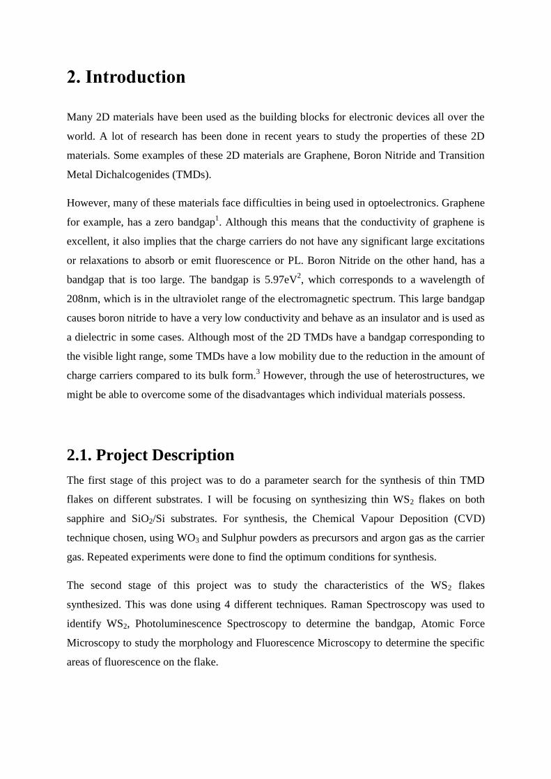
2.2. Transition Metal Dichalcogenides (TMDs)
Atomically thin sheets of TMDs are a promising class of materials for a range of
applications.4 These materials are made to complement or even replace certain standard
materials being used in semiconductor devices currently.5 One reason for this is due to the
direct bandgap the 2D TMDs possess. The concept of a direct bandgap is illustrated in the
diagram below.
Fig 1: Energy profile diagram of direct and indirect bandgaps
Bulk TMDs possess an indirect bandgap. This means that for an electron to transfer from the
valence band to the conduction band, a photon and a phonon is needed, as illustrated in the
figure above. However, when a TMD monolayer is used instead, the bandgap changes to a
direct bandgap.6 This means that only a photon is needed for the excitation of an electron.
This allows the material to exhibit fluorescence and photoluminescence which is useful for
optoelectronics.
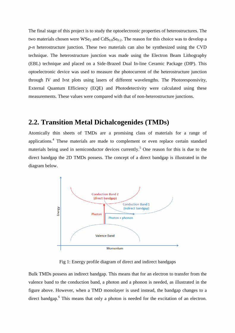
Thin 2D TMDs can be synthesized by a few methods. The exfoliation technique can be used,
where a thin layer of TMD can be mechanically cleaved off of a bulk TMD using an adhesive
tape. This is possible due to the structure of TMDs.4 Similar to graphene, TMDs consists of
layers of covalent bonds. This can be seen in the figure below which shows the monolayer
structure for MoS2.
Fig 2: Atomic structure of monolayer MoS2. (© Johnny Wong, University of Twente)
In a bulk TMD, the monolayers are bonded to each other through weak Van Der Waals
forces.4 This explains why the exfoliation technique is appropriate in synthesizing thin 2D
TMDs. However, this technique has a low yield and has little control over the thickness of the
TMD flake obtained.7
In my project, I will be using the Chemical Vapour Deposition technique to synthesize 2D
TMDs. This technique will be elaborated in the following section of my report.
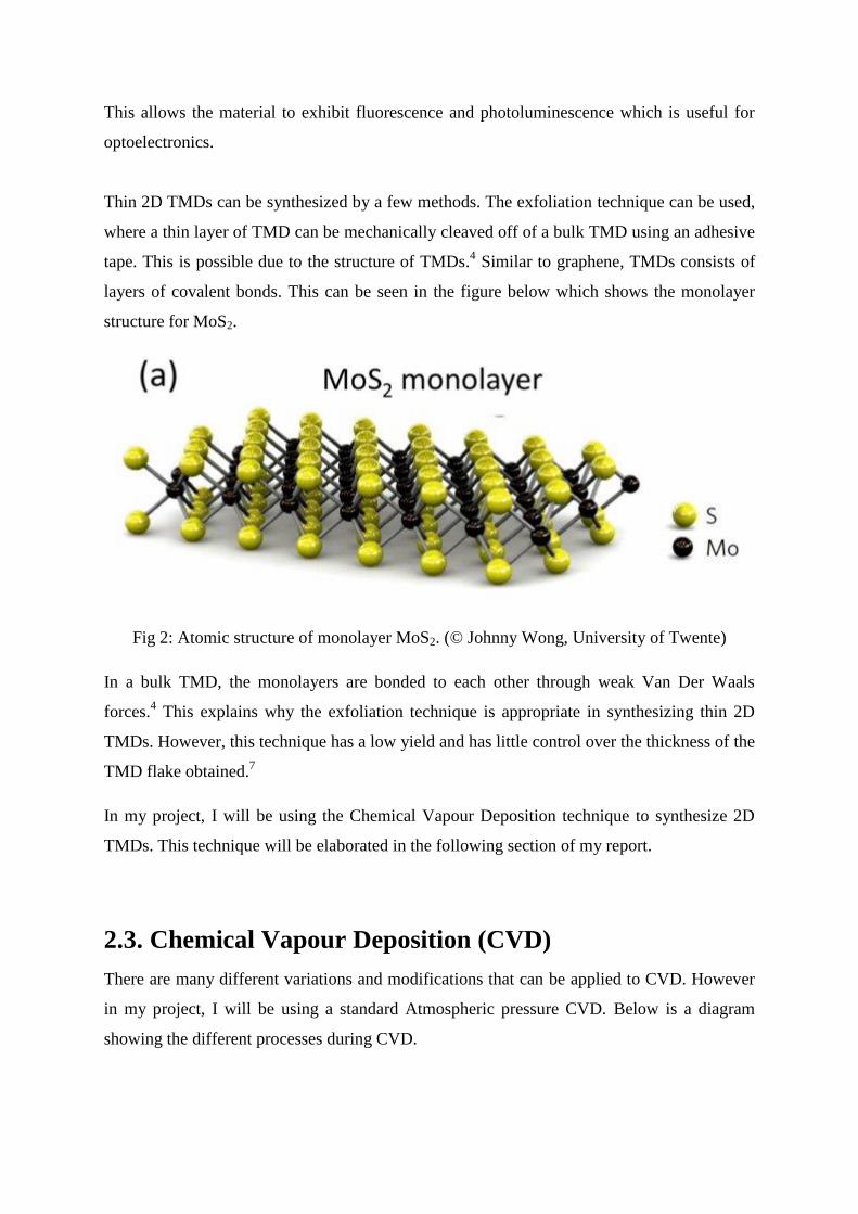
2.3. Chemical Vapour Deposition (CVD)
There are many different variations and modifications that can be applied to CVD. However
in my project, I will be using a standard Atmospheric pressure CVD. Below is a diagram
showing the different processes during CVD.
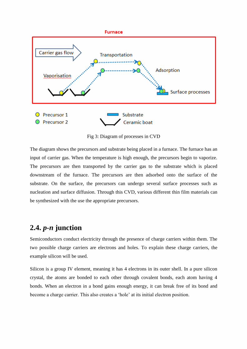
Fig 3: Diagram of processes in CVD
The diagram shows the precursors and substrate being placed in a furnace. The furnace has an
input of carrier gas. When the temperature is high enough, the precursors begin to vaporize.
The precursors are then transported by the carrier gas to the substrate which is placed
downstream of the furnace. The precursors are then adsorbed onto the surface of the
substrate. On the surface, the precursors can undergo several surface processes such as
nucleation and surface diffusion. Through this CVD, various different thin film materials can
be synthesized with the use the appropriate precursors.
2.4. p-n junction
Semiconductors conduct electricity through the presence of charge carriers within them. The
two possible charge carriers are electrons and holes. To explain these charge carriers, the
example silicon will be used.
Silicon is a group IV element, meaning it has 4 electrons in its outer shell. In a pure silicon
crystal, the atoms are bonded to each other through covalent bonds, each atom having 4
bonds. When an electron in a bond gains enough energy, it can break free of its bond and
become a charge carrier. This also creates a ‘hole’ at its initial electron position.
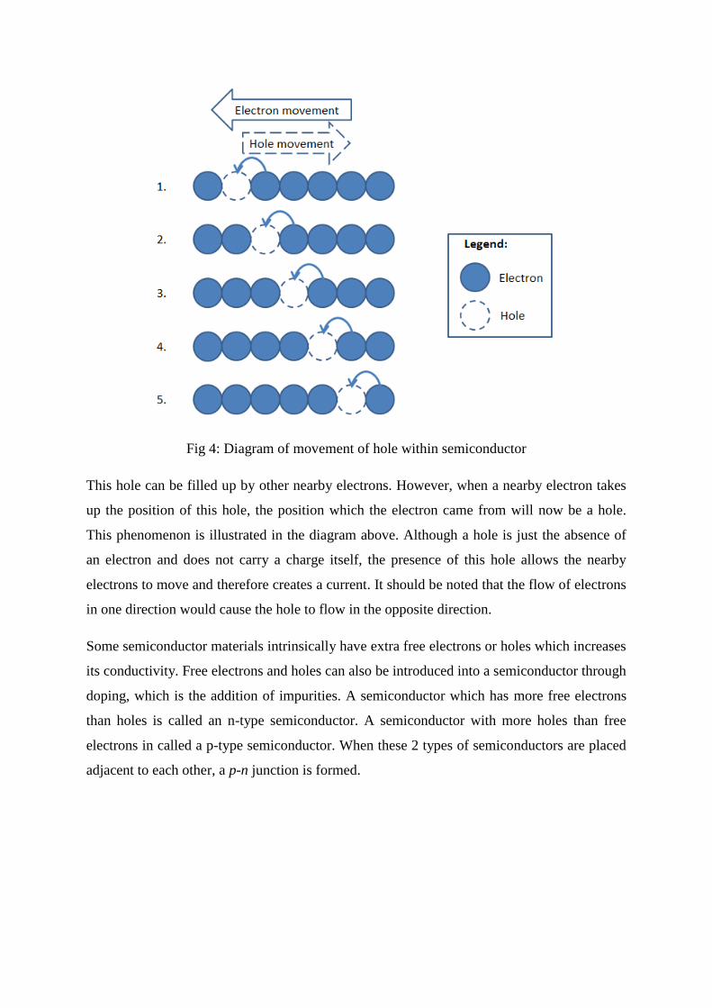
Fig 4: Diagram of movement of hole within semiconductor
This hole can be filled up by other nearby electrons. However, when a nearby electron takes
up the position of this hole, the position which the electron came from will now be a hole.
This phenomenon is illustrated in the diagram above. Although a hole is just the absence of
an electron and does not carry a charge itself, the presence of this hole allows the nearby
electrons to move and therefore creates a current. It should be noted that the flow of electrons
in one direction would cause the hole to flow in the opposite direction.
Some semiconductor materials intrinsically have extra free electrons or holes which increases
its conductivity. Free electrons and holes can also be introduced into a semiconductor through
doping, which is the addition of impurities. A semiconductor which has more free electrons
than holes is called an n-type semiconductor. A semiconductor with more holes than free
electrons in called a p-type semiconductor. When these 2 types of semiconductors are placed
adjacent to each other, a p-n junction is formed.
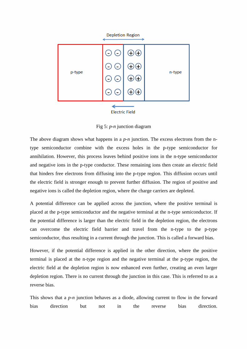
Fig 5: p-n junction diagram
The above diagram shows what happens in a p-n junction. The excess electrons from the n-
type semiconductor combine with the excess holes in the p-type semiconductor for
annihilation. However, this process leaves behind positive ions in the n-type semiconductor
and negative ions in the p-type conductor. These remaining ions then create an electric field
that hinders free electrons from diffusing into the p-type region. This diffusion occurs until
the electric field is stronger enough to prevent further diffusion. The region of positive and
negative ions is called the depletion region, where the charge carriers are depleted.
A potential difference can be applied across the junction, where the positive terminal is
placed at the p-type semiconductor and the negative terminal at the n-type semiconductor. If
the potential difference is larger than the electric field in the depletion region, the electrons
can overcome the electric field barrier and travel from the n-type to the p-type
semiconductor, thus resulting in a current through the junction. This is called a forward bias.
However, if the potential difference is applied in the other direction, where the positive
terminal is placed at the n-type region and the negative terminal at the p-type region, the
electric field at the depletion region is now enhanced even further, creating an even larger
depletion region. There is no current through the junction in this case. This is referred to as a
reverse bias.
This shows that a p-n junction behaves as a diode, allowing current to flow in the forward
bias direction but not in the reverse bias direction.
3. Methodology
3.1. Synthesis of WS2 through Chemical Vapour
Deposition (CVD)
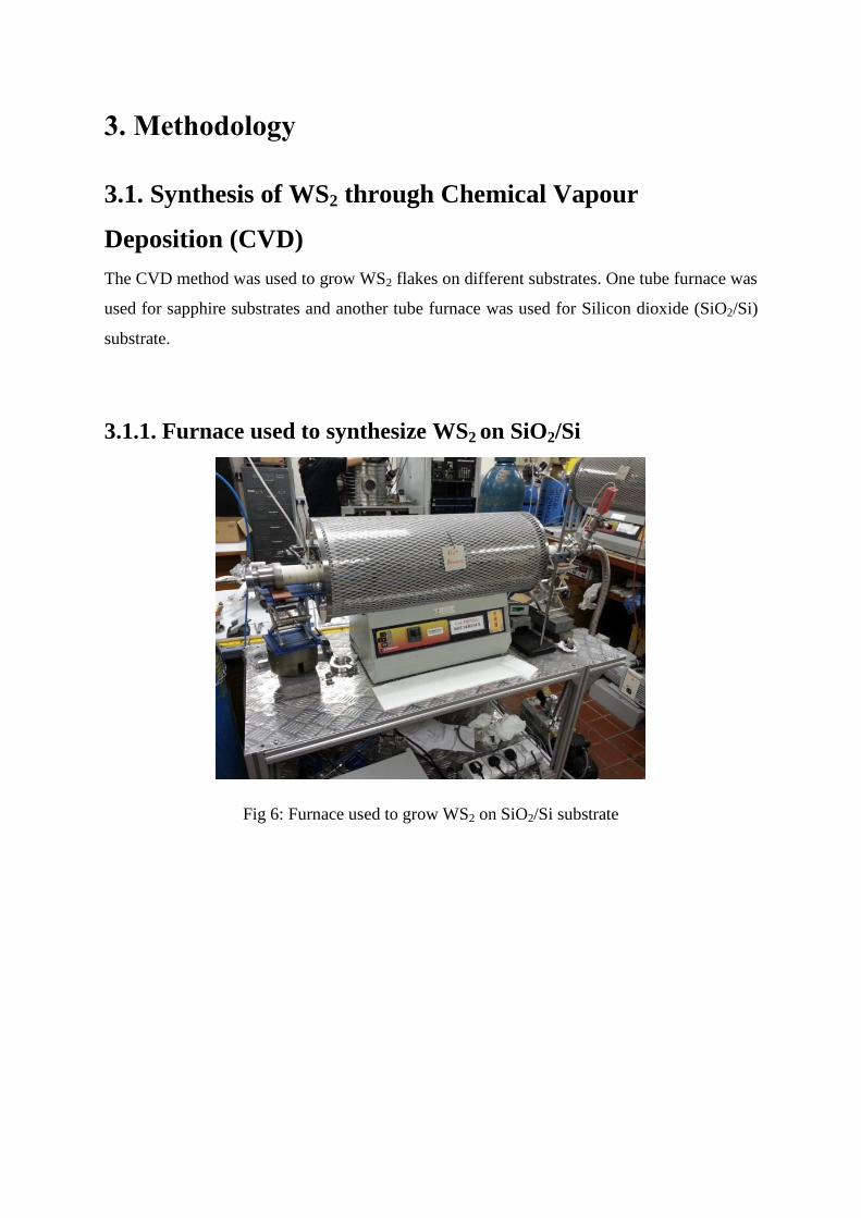
The CVD method was used to grow WS2 flakes on different substrates. One tube furnace was
used for sapphire substrates and another tube furnace was used for Silicon dioxide (SiO2/Si)
substrate.
3.1.1. Furnace used to synthesize WS2 on SiO2/Si
Fig 6: Furnace used to grow WS2 on SiO2/Si substrate
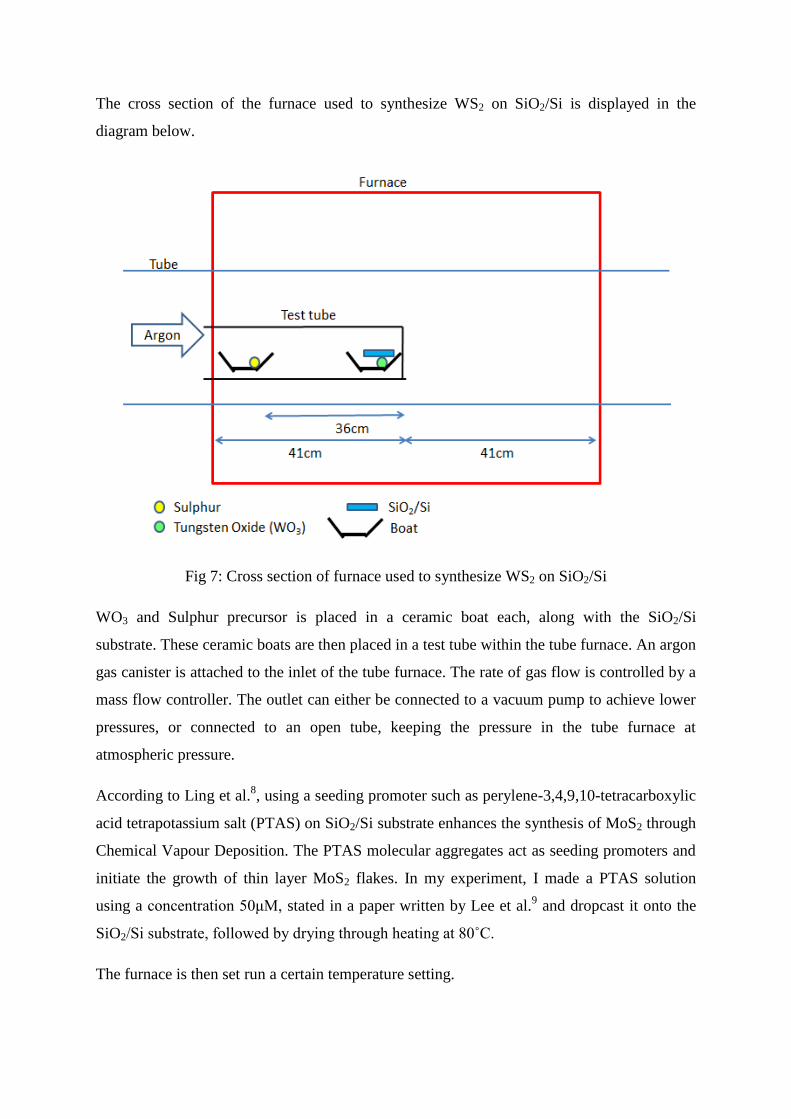
The cross section of the furnace used to synthesize WS2 on SiO2/Si is displayed in the
diagram below.
Fig 7: Cross section of furnace used to synthesize WS2 on SiO2/Si
WO3 and Sulphur precursor is placed in a ceramic boat each, along with the SiO2/Si
substrate. These ceramic boats are then placed in a test tube within the tube furnace. An argon
gas canister is attached to the inlet of the tube furnace. The rate of gas flow is controlled by a
mass flow controller. The outlet can either be connected to a vacuum pump to achieve lower
pressures, or connected to an open tube, keeping the pressure in the tube furnace at
atmospheric pressure.
According to Ling et al.8, using a seeding promoter such as perylene-3,4,9,10-tetracarboxylic
acid tetrapotassium salt (PTAS) on SiO2/Si substrate enhances the synthesis of MoS2 through
Chemical Vapour Deposition. The PTAS molecular aggregates act as seeding promoters and
initiate the growth of thin layer MoS2 flakes. In my experiment, I made a PTAS solution
using a concentration 50μM, stated in a paper written by Lee et al.9 and dropcast it onto the
SiO2/Si substrate, followed by drying through heating at 80˚C.
The furnace is then set run a certain temperature setting.
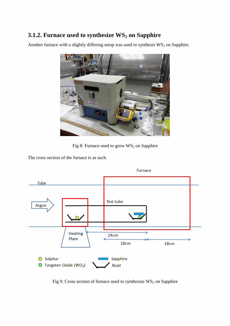
3.1.2. Furnace used to synthesize WS2 on Sapphire
Another furnace with a slightly differing setup was used to synthesis WS2 on Sapphire.
Fig 8: Furnace used to grow WS2 on Sapphire
The cross section of the furnace is as such.
Fig 9: Cross section of furnace used to synthesize WS2 on Sapphire
The setup of this furnace is very similar to the furnace used to synthesize WS2 on SiO2/Si.
However, instead of having the Sulphur precursor boat being in the furnace, it is placed
outside the furnace, under a heating plate. The heating plate helps to control the temperature
of the Sulphur separately. The Sulphur was heated to a temperature of 290˚C. According to
Peimyoo et al.10
, heating the Sulphur separately helps in a more uniform growth of the WS2
flakes.
The gas flow was also controlled by a mass flow controller and the outlet was also open to
the atmospheric pressure.
The furnace is then set run a certain temperature setting.
3.2. Characterisation of WS2
I used 4 techniques to study the WS2 flakes synthesized. The four techniques are Raman
Spectroscopy, Photoluminescence Spectroscopy, Fluorescence Microscopy and Atomic Force
Microscopy. Each of these methods helps us to study an aspect of the WS2 flakes.
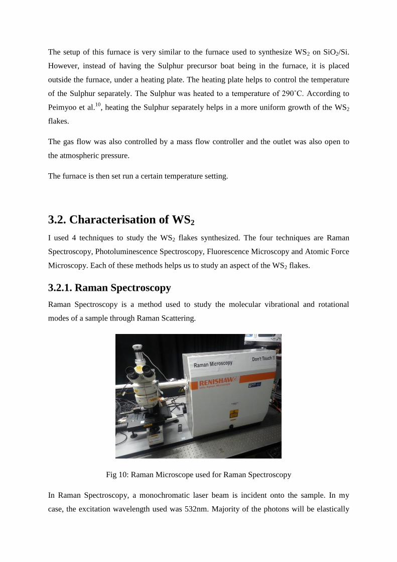
3.2.1. Raman Spectroscopy
Raman Spectroscopy is a method used to study the molecular vibrational and rotational
modes of a sample through Raman Scattering.
Fig 10: Raman Microscope used for Raman Spectroscopy
In Raman Spectroscopy, a monochromatic laser beam is incident onto the sample. In my
case, the excitation wavelength used was 532nm. Majority of the photons will be elastically
scattered, also known as Rayleigh scattering, which means that they will be the same
wavelength as the incident photons. However, there will be a small portion of photons which
will be inelastically scattered, which is called Raman Scattering. This is due to the laser
photons interacting with the molecular vibrations of the sample. Raman Scattering
wavelengths deviate from the excitation wavelength to extents, depending on the vibrational
modes present. This gives each material a specific Raman spectrum.
Often after a synthesis process, there are many microscopic objects of different shapes and
sizes on the substrate that can be seen optically. Raman spectroscopy can also be used to
identify and confirm what is seen.
The graphs of Raman Spectroscopy plot the Intensity of scattered photons against the shift in
wavenumber with respect to the incident photon’s wavenumber.
3.2.2. Photoluminescence (PL) Spectroscopy
According to Gfroerer11
, PL is the spontaneous emission of light from a material under
optical excitation. PL Spectroscopy is a non-destructive method used to study the optical
properties of a material. A photon of a higher frequency and energy is incident onto the
sample. For my PL Spectroscopy, I used an excitation wavelength of 532nm to incident onto
the WS2 flake. This photon causes electrons in the material to excite to a higher energy level,
overcoming its bandgap. Following this, the electron will undergo relaxation processes. The
relaxation across the bandgap will occur as an emission of a photon, which is the PL
observed. PL Spectroscopy plots the intensity of PL detected against wavelength. PL
Spectroscopy helped to determine the bandgap of the WS2 flake.
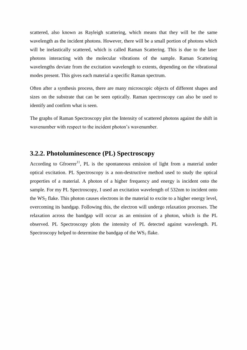
3.2.3. Atomic Force Microscopy (AFM)
Fig 11: Setup of Atomic Force Microscopy. (© Edinformatics.com)
Tapping mode Atomic Force Microscopy (AFM) is a method used to study the morphology
of a material’s surface. The setup is as shown above. A cantilever and tip are used as a probe
to map out the surface of the sample. When the tip is brought close to the surface, various
different forces between the surface and the tip will cause the angle of deflection of the laser
to change. These deflections are detected by a photodiode acting as a detector. The
photodiode will then feedback to the system to adjust the tip-to-sample distance. This is to
prevent the tip from being damaged by the surface. These changes will correspond to the
height of the point on the surface, which is then recorded. The cantilever will go back and
forth along the surface and slowly plot out the morphology of the surface.
3.2.4. Fluorescence Microscopy
Fluorescence Microscopy is commonly used in today’s research, especially in the fields of
Biology. It is very good for visual detection and tracking of certain cells which might exhibit
specific fluorescence. Certain dyes can be used to coat certain materials for easy tracking.
Fluorescence occurs when photons of a higher energy, compared to that of the bandgap of a
material, is incident onto the material. If the photon is within the absorption range of the
material, the photon will excite the electron into a higher energy state. The electron will then
release energy through photons and other forms of vibrations. The photon emitted by the
electron when dropping back down the bandgap is the fluorescence seen. This is very similar
to PL mentioned earlier. In Fluorescence Microscopy however, an optical image of the
fluorescence is taken rather than an intensity plot of fluorescence. This helps us to visually
see which points on the WS2 flake emit fluorescence.
3.3. Optoelectronic Device
An optoelectronic device was made to study the properties of the junction through IV and
Ivst graphs. WSe2 flakes were used instead of WS2 flakes. The reason for this choice will
discussed in section 4.3.
3.3.1. Fabrication of Optoelectronic Device
First, Polymethyl Methacrylate (PMMA) is applied onto the substrate containing the WSe2
flake. It is spin coated and then baked. This material polymer is used as a photoresist. After a
layer of PMMA is formed, the substrate is put into an EBL chamber where the electron beam
is used to draw out the position desired for the electrode. According to Choi et al.12
, the
electron beam causes chain scission within the PMMA which degrades it. The substrate is
then placed in photoresist developer which dissolves away only the degraded PMMA.
Following this the substrate is washed with DI water and dried with Nitrogen gas. The
substrate is then put into a thermal evaporator with 2 heating sources within it, one with Gold
(Au) and the other Palladium (Pd). A layer of Palladium of 20nm thick is deposited on the
substrate followed by 80nm of Gold. Following this, Acetone is used to remove the
remaining PMMA on the substrate, leaving behind Pd/Au electrodes at the desired positions.
The process is finished off by washing the substrate in DI water and dried with Nitrogen gas.
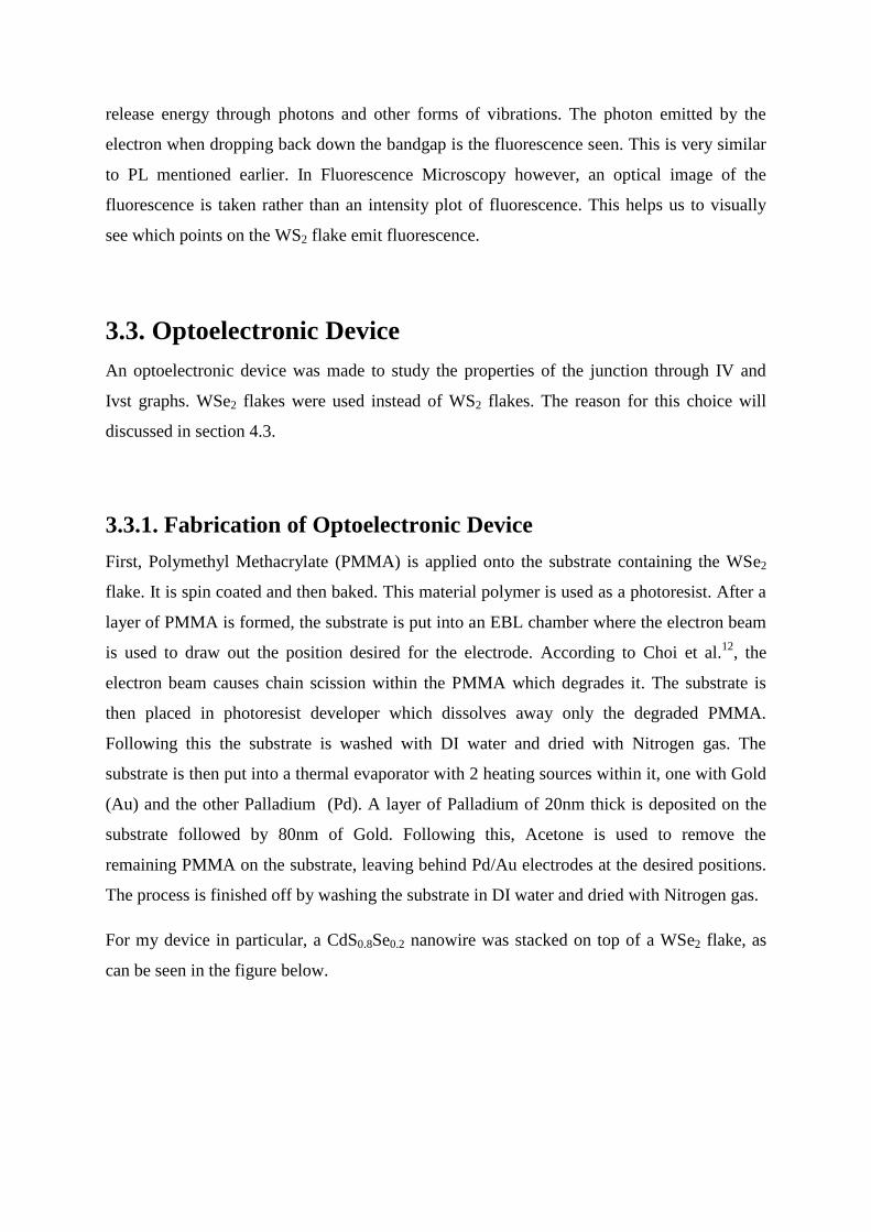
For my device in particular, a CdS0.8Se0.2 nanowire was stacked on top of a WSe2 flake, as
can be seen in the figure below.
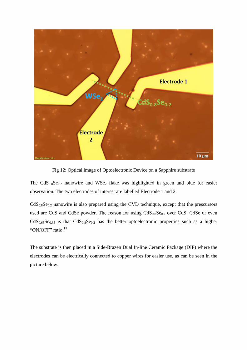
Fig 12: Optical image of Optoelectronic Device on a Sapphire substrate
The CdS0.8Se0.2 nanowire and WSe2 flake was highlighted in green and blue for easier
observation. The two electrodes of interest are labelled Electrode 1 and 2.
CdS0.8Se0.2 nanowire is also prepared using the CVD technique, except that the prescursors
used are CdS and CdSe powder. The reason for using CdS0.8Se0.2 over CdS, CdSe or even
CdS0.65Se0.35 is that CdS0.8Se0.2 has the better optoelectronic properties such as a higher
“ON/OFF” ratio.13
The substrate is then placed in a Side-Brazen Dual In-line Ceramic Package (DIP) where the
electrodes can be electrically connected to copper wires for easier use, as can be seen in the
picture below.
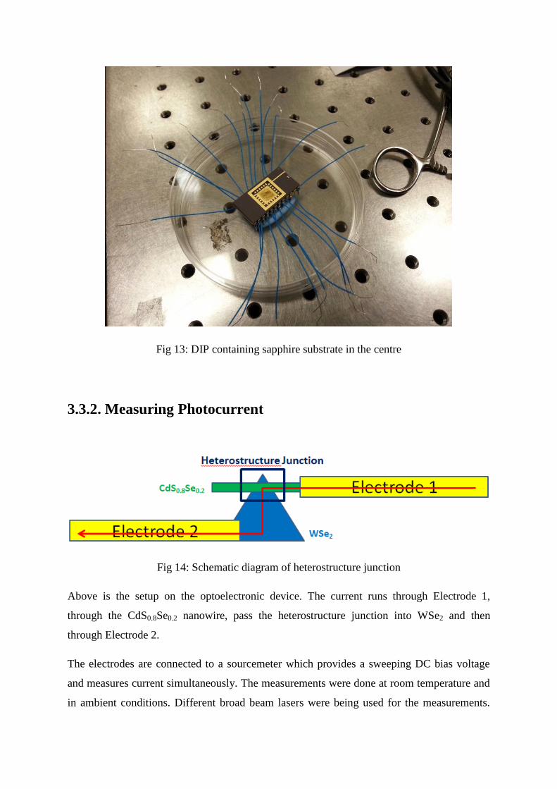
Fig 13: DIP containing sapphire substrate in the centre
3.3.2. Measuring Photocurrent
Fig 14: Schematic diagram of heterostructure junction
Above is the setup on the optoelectronic device. The current runs through Electrode 1,
through the CdS0.8Se0.2 nanowire, pass the heterostructure junction into WSe2 and then
through Electrode 2.
The electrodes are connected to a sourcemeter which provides a sweeping DC bias voltage
and measures current simultaneously. The measurements were done at room temperature and
in ambient conditions. Different broad beam lasers were being used for the measurements.

The lasers were mounted on a tripod stand and incident upon the substrate, ensuring that the
entire heterostructure junction and the electrodes contact with the WSe2 flake and CdS0.8Se0.2
nanowire are uniformly illuminated. This is called global irradiation. Measurements were
done for both dark current and with laser incidence of different wavelengths.
Besides IV graphs, current against time (Ivst) graphs were measured as well. During the
measurement, the laser used is being blocked and unblocked approximately every 5 seconds.
The “ON” state refers to when the laser is unblocked and “OFF” when the laser is blocked.
This way, the difference between dark current and the current under illumination can be
measured.
4. Results
4.1. Synthesis of WS2 with CVD
A majority of my time spent on this project was on doing parameter searches for the optimum
conditions for growth of WS2 on sapphire and SiO2/Si. Approximately 160 CVDs were done
in this project. It was very difficult to find optimum conditions as it was difficult to get
consistent results with apparently the same parameters. It was probably the case that there
were a few parameters I was unaware of that affected the growth of the TMD flakes. These
parameters were not controlled and therefore leading to apparently inconsistent results.
Across time, I did manage to find out a few of these parameters, but definitely not all.
However, I did manage to find my best set parameters that have been giving me rather
consistent growth for sapphire and SiO2/Si substrates. Although definitely not with 100%
consistency for good growth, this was the best set of parameters I could find out during my
time doing this project.
4.1.1. Synthesis on SiO2/Si substrate
There were many variations being made in the parameter search for synthesis of WS2.
4.1.1.1. Position of substrate
The substrate was placed at different distances away from the WO3 precursor within that
ceramic boat for different CVDs. It was even placed at different positions in between the
ceramic boats along the test tube. For the SiO2/Si substrate, there is only 1 side which is used
for the synthesis of TMD flakes. For many of these positions along the furnace, the substrate
was tested both facing up and facing down. The size of the substrate was also varied for some
of the positions. We discovered that the optimised position for the SiO2/Si substrate was to
place it face down, right above the WO3 precursor, as shown in the figure below.
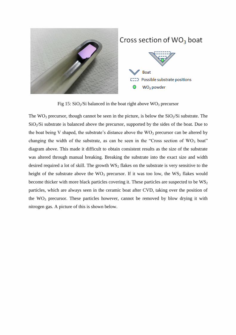
Fig 15: SiO2/Si balanced in the boat right above WO3 precursor
The WO3 precursor, though cannot be seen in the picture, is below the SiO2/Si substrate. The
SiO2/Si substrate is balanced above the precursor, supported by the sides of the boat. Due to
the boat being V shaped, the substrate’s distance above the WO3 precursor can be altered by
changing the width of the substrate, as can be seen in the “Cross section of WO3 boat”
diagram above. This made it difficult to obtain consistent results as the size of the substrate
was altered through manual breaking. Breaking the substrate into the exact size and width
desired required a lot of skill. The growth WS2 flakes on the substrate is very sensitive to the
height of the substrate above the WO3 precursor. If it was too low, the WS2 flakes would
become thicker with more black particles covering it. These particles are suspected to be WS2
particles, which are always seen in the ceramic boat after CVD, taking over the position of
the WO3 precursor. These particles however, cannot be removed by blow drying it with
nitrogen gas. A picture of this is shown below.
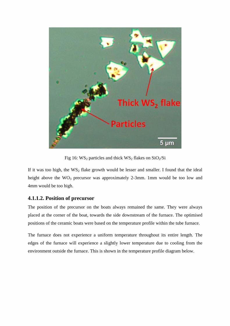
Fig 16: WS2 particles and thick WS2 flakes on SiO2/Si
If it was too high, the WS2 flake growth would be lesser and smaller. I found that the ideal
height above the WO3 precursor was approximately 2-3mm. 1mm would be too low and
4mm would be too high.
4.1.1.2. Position of precursor
The position of the precursor on the boats always remained the same. They were always
placed at the corner of the boat, towards the side downstream of the furnace. The optimised
positions of the ceramic boats were based on the temperature profile within the tube furnace.
The furnace does not experience a uniform temperature throughout its entire length. The
edges of the furnace will experience a slightly lower temperature due to cooling from the
environment outside the furnace. This is shown in the temperature profile diagram below.
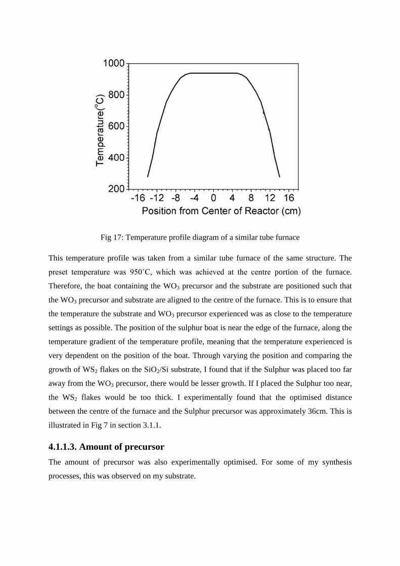
Fig 17: Temperature profile diagram of a similar tube furnace
This temperature profile was taken from a similar tube furnace of the same structure. The
preset temperature was 950˚C, which was achieved at the centre portion of the furnace.
Therefore, the boat containing the WO3 precursor and the substrate are positioned such that
the WO3 precursor and substrate are aligned to the centre of the furnace. This is to ensure that
the temperature the substrate and WO3 precursor experienced was as close to the temperature
settings as possible. The position of the sulphur boat is near the edge of the furnace, along the
temperature gradient of the temperature profile, meaning that the temperature experienced is
very dependent on the position of the boat. Through varying the position and comparing the
growth of WS2 flakes on the SiO2/Si substrate, I found that if the Sulphur was placed too far
away from the WO3 precursor, there would be lesser growth. If I placed the Sulphur too near,
the WS2 flakes would be too thick. I experimentally found that the optimised distance
between the centre of the furnace and the Sulphur precursor was approximately 36cm. This is
illustrated in Fig 7 in section 3.1.1.
4.1.1.3. Amount of precursor
The amount of precursor was also experimentally optimised. For some of my synthesis
processes, this was observed on my substrate.
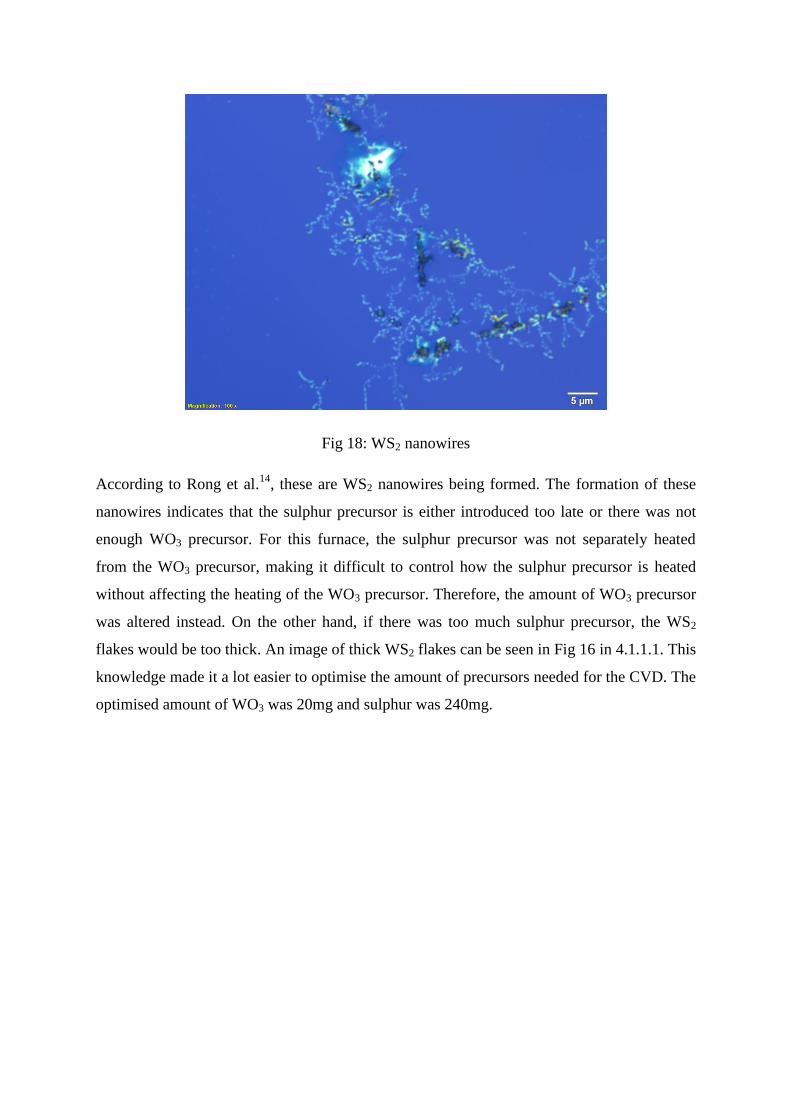
Fig 18: WS2 nanowires
According to Rong et al.14
, these are WS2 nanowires being formed. The formation of these
nanowires indicates that the sulphur precursor is either introduced too late or there was not
enough WO3 precursor. For this furnace, the sulphur precursor was not separately heated
from the WO3 precursor, making it difficult to control how the sulphur precursor is heated
without affecting the heating of the WO3 precursor. Therefore, the amount of WO3 precursor
was altered instead. On the other hand, if there was too much sulphur precursor, the WS2
flakes would be too thick. An image of thick WS2 flakes can be seen in Fig 16 in 4.1.1.1. This
knowledge made it a lot easier to optimise the amount of precursors needed for the CVD. The
optimised amount of WO3 was 20mg and sulphur was 240mg.
4.1.1.4. Temperature
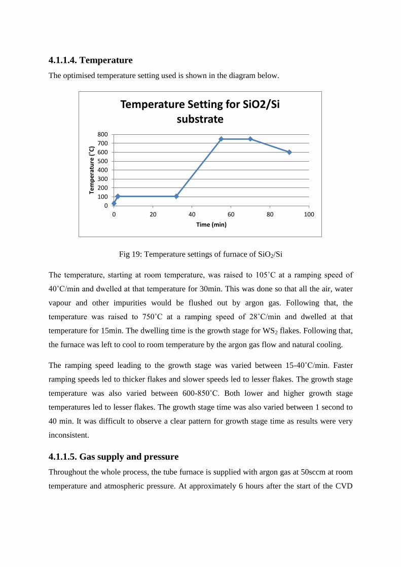
The optimised temperature setting used is shown in the diagram below.
Fig 19: Temperature settings of furnace of SiO2/Si
The temperature, starting at room temperature, was raised to 105˚C at a ramping speed of
40˚C/min and dwelled at that temperature for 30min. This was done so that all the air, water
vapour and other impurities would be flushed out by argon gas. Following that, the
temperature was raised to 750˚C at a ramping speed of 28˚C/min and dwelled at that
temperature for 15min. The dwelling time is the growth stage for WS2 flakes. Following that,
the furnace was left to cool to room temperature by the argon gas flow and natural cooling.
The ramping speed leading to the growth stage was varied between 15-40˚C/min. Faster
ramping speeds led to thicker flakes and slower speeds led to lesser flakes. The growth stage
temperature was also varied between 600-850˚C. Both lower and higher growth stage
temperatures led to lesser flakes. The growth stage time was also varied between 1 second to
40 min. It was difficult to observe a clear pattern for growth stage time as results were very
inconsistent.
4.1.1.5. Gas supply and pressure
Throughout the whole process, the tube furnace is supplied with argon gas at 50sccm at room
temperature and atmospheric pressure. At approximately 6 hours after the start of the CVD
0
100
200
300
400
500
600
700
800
0 20 40 60 80 100
Tem
pe
ratu
re (
˚C)
Time (min)
Temperature Setting for SiO2/Si substrate
process, the tube furnace would be approximately 350˚C. This is when the argon gas supply
is stopped and the tube furnace is left to cool through natural cooling.
The rate of gas supply input was varied from 50-200sccm. Using faster rates led to thicker
flakes. The pressure within the tube furnace was also varied between 0.57Torr to atmospheric
pressure. Lower pressure was achieved through connecting the outlet of the tube furnace to a
vacuum pump. Lower pressures led to lesser flake growth.
4.1.1.6. Cleaning substrate using Piranha solution
One of the suspicions for bad growth of WS2 flakes was that the substrates used were not
clean enough. Therefore, the substrates were washed in Piranha solution before using it for
CVD. The Piranha solution consists of aqueous Sulphuric Acid and Hydrogen Peroxide. The
concentrations of Hydrogen Peroxide and Sulphuric acid used were 30w/w and 98%w/w
respectively. The ratio of volume of Sulphuric Acid to Hydrogen Peroxide was 3:1. The
substrate was left inside the solution for approximately 16 hours. The substrates were then
taken out, washed with DI water and dried with nitrogen gas. However, we found that this
caused even less WS2 growth. I speculate that it is because certain particles can acts as
nucleation sites for the WS2 flake. I did not use the Piranha solution in my ideal parameters
for growth of thin WS2 flakes.
4.1.1.7. Si3N4
In the later portion of my project, we tried to use the WS2 flakes on SiO2/Si substrate to make
an optoelectronic device. However after running some tests, we realized that current could
flow through SiO2/Si surface itself, meaning that the current was not isolated to the WS2 flake
or CdS0.8Se0.2 nanowire. This meant that the dielectric layer on the SiO2/Si was spoilt. We
speculate that it is probably due to the high heat during the CVD process. I started using
Si3N4 instead of SiO2/Si for my CVD process, using the same parameters. There was
successful growth of thin WS2 flakes. However, I did not have time to make an
optoelectronic device out of it due to time constraints.
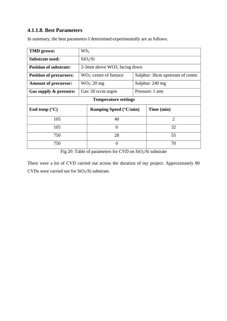
4.1.1.8. Best Parameters
In summary, the best parameters I determined experimentally are as follows.
TMD grown: WS2
Substrate used: SiO2/Si
Position of substrate: 2-3mm above WO3, facing down
Position of precursors: WO3: centre of furnace Sulphur: 36cm upstream of centre
Amount of precursor: WO3: 20 mg Sulphur: 240 mg
Gas supply & pressure: Gas: 50 sccm argon Pressure: 1 atm
Temperature settings
End temp (°C) Ramping Speed (°C/min) Time (min)
105 40 2
105 0 32
750 28 55
750 0 70
Fig 20: Table of parameters for CVD on SiO2/Si substrate
There were a lot of CVD carried out across the duration of my project. Approximately 80
CVDs were carried out for SiO2/Si substrate.
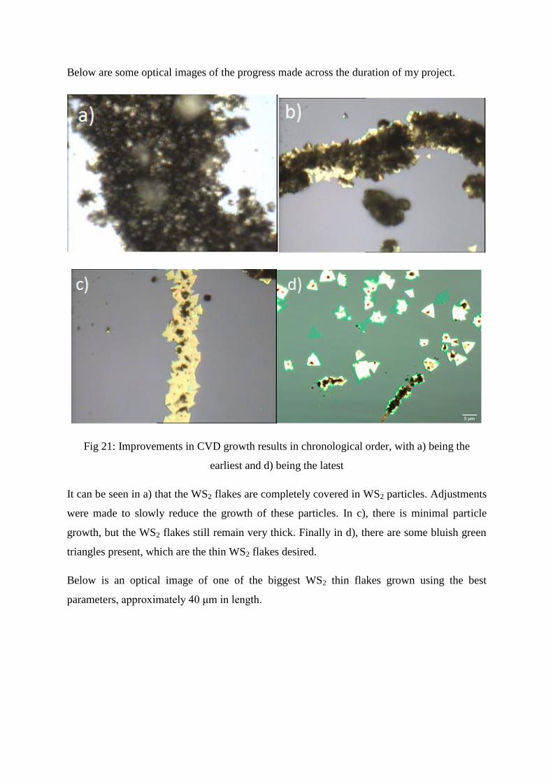
Below are some optical images of the progress made across the duration of my project.
Fig 21: Improvements in CVD growth results in chronological order, with a) being the
earliest and d) being the latest
It can be seen in a) that the WS2 flakes are completely covered in WS2 particles. Adjustments
were made to slowly reduce the growth of these particles. In c), there is minimal particle
growth, but the WS2 flakes still remain very thick. Finally in d), there are some bluish green
triangles present, which are the thin WS2 flakes desired.
Below is an optical image of one of the biggest WS2 thin flakes grown using the best
parameters, approximately 40 μm in length.
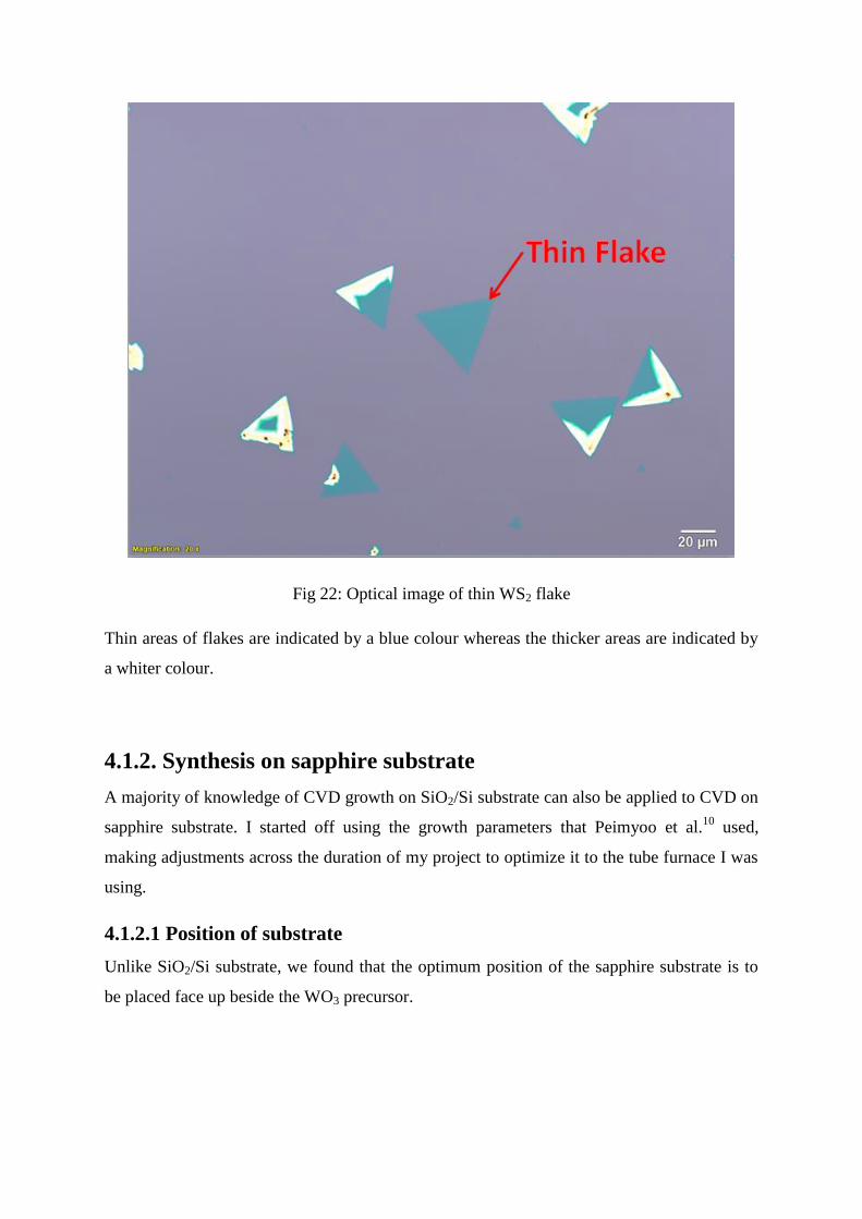
Fig 22: Optical image of thin WS2 flake
Thin areas of flakes are indicated by a blue colour whereas the thicker areas are indicated by
a whiter colour.
4.1.2. Synthesis on sapphire substrate
A majority of knowledge of CVD growth on SiO2/Si substrate can also be applied to CVD on
sapphire substrate. I started off using the growth parameters that Peimyoo et al.10
used,
making adjustments across the duration of my project to optimize it to the tube furnace I was
using.
4.1.2.1 Position of substrate
Unlike SiO2/Si substrate, we found that the optimum position of the sapphire substrate is to
be placed face up beside the WO3 precursor.
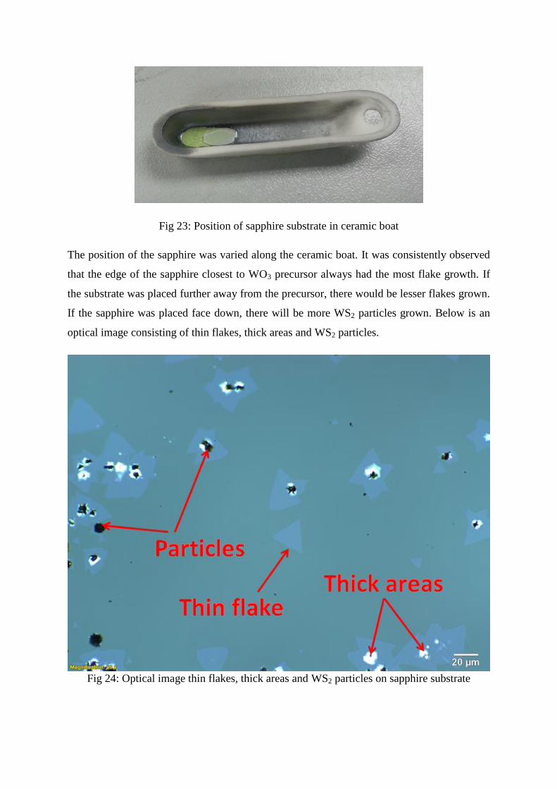
Fig 23: Position of sapphire substrate in ceramic boat
The position of the sapphire was varied along the ceramic boat. It was consistently observed
that the edge of the sapphire closest to WO3 precursor always had the most flake growth. If
the substrate was placed further away from the precursor, there would be lesser flakes grown.
If the sapphire was placed face down, there will be more WS2 particles grown. Below is an
optical image consisting of thin flakes, thick areas and WS2 particles.
Fig 24: Optical image thin flakes, thick areas and WS2 particles on sapphire substrate
4.1.2.2. Position of precursor
The WO3 precursor was always placed at the corner of the ceramic boat, towards the side
downstream of the furnace. Due to the amount of Sulphur precursor and the size of its
ceramic boat, the Sulphur precursor always took up the entire ceramic boat. Following the
same principle as with CVD using SiO2/Si, the WO3 precursor and sapphire was positioned in
the centre of the furnace ensuring it experiences the most accurate temperature. Since for this
CVD the Sulphur precursor is separately heated by a heating plate, there was no need to
adjust the position of it. The Sulphur precursor was placed 25 cm away from the centre of the
furnace and the WO3 precursor.
4.1.2.3. Amount of precursor
Using the same knowledge for growth on SiO2/Si substrate, I found the optimum amount of
precursors used is 20 mg of WO3 and 200 mg of Sulphur.
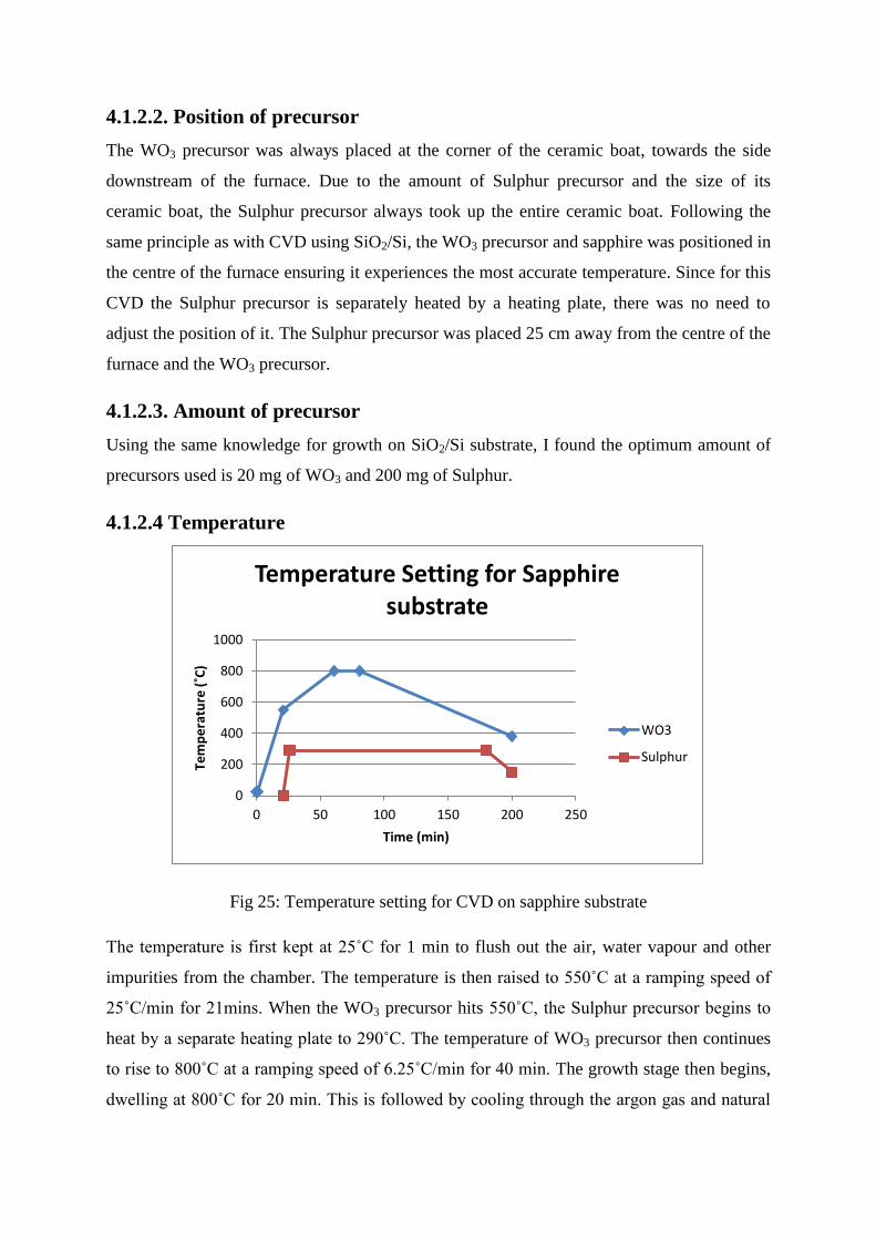
4.1.2.4 Temperature
Fig 25: Temperature setting for CVD on sapphire substrate
The temperature is first kept at 25˚C for 1 min to flush out the air, water vapour and other
impurities from the chamber. The temperature is then raised to 550˚C at a ramping speed of
25˚C/min for 21mins. When the WO3 precursor hits 550˚C, the Sulphur precursor begins to
heat by a separate heating plate to 290˚C. The temperature of WO3 precursor then continues
to rise to 800˚C at a ramping speed of 6.25˚C/min for 40 min. The growth stage then begins,
dwelling at 800˚C for 20 min. This is followed by cooling through the argon gas and natural
0
200
400
600
800
1000
0 50 100 150 200 250
Tem
pe
ratu
re (
˚C)
Time (min)
Temperature Setting for Sapphire substrate
WO3
Sulphur
cooling. After approximately 3 hours, the WO3 precursor reaches approximately 400˚C. This
is when the heating plate beneath the Sulphur precursor is turned off.
The ramping speed for the WO3 precursor from 550˚C to 800˚C was varied between 5-
10˚C/min. A higher ramping speed caused thicker flake growth. The growth stage
temperature was varied between 750-850˚C. Using a higher temperature caused lesser flake
growth. However, 750-800˚C seemed to have equally good growth. The growth stage
duration was also varied between 10-20 mins. A shorter duration caused lesser flake growth.
4.1.2.5. Gas Supply and Pressure
Through the whole CVD, the chamber is supplied with 200sccm of argon gas at atmospheric
pressure. Approximately after 6 hours after the start of the CVD, the chamber will reach
between 100-200˚C. The gas supply is turned off and the tube furnace is left to cool by
natural cooling.
The argon supply was varied between 100-200sccm. A lower rate would lead to lesser growth
of WS2 flakes.
4.1.2.6. Sulphur-rich environment.
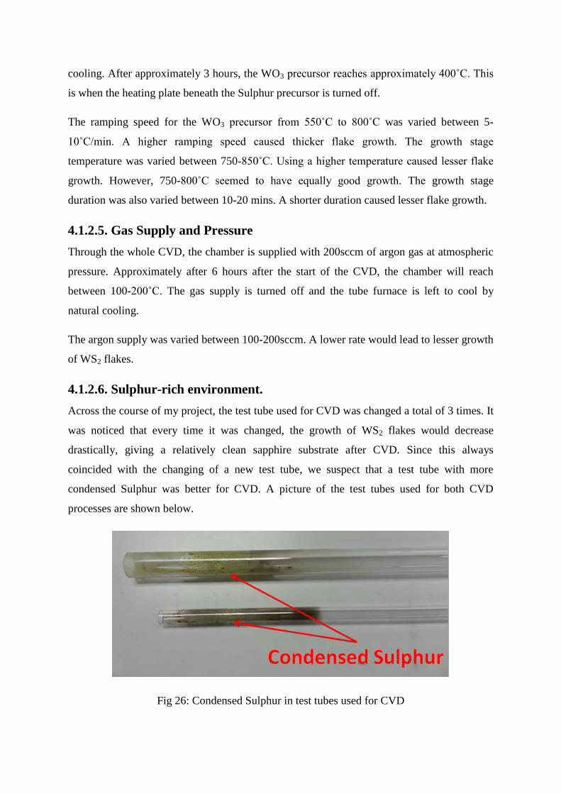
Across the course of my project, the test tube used for CVD was changed a total of 3 times. It
was noticed that every time it was changed, the growth of WS2 flakes would decrease
drastically, giving a relatively clean sapphire substrate after CVD. Since this always
coincided with the changing of a new test tube, we suspect that a test tube with more
condensed Sulphur was better for CVD. A picture of the test tubes used for both CVD
processes are shown below.
Fig 26: Condensed Sulphur in test tubes used for CVD
The amount of condensed Sulphur is proportional to the number of CVDs it has undergone. It
takes approximately 7 CVDs for a new test tube to obtain sufficient condensed Sulphur for
the growth of thin WS2 flakes. I suspect this creates a Sulphur-rich environment for the WO3
precursor and sapphire substrate, helping the growth of WS2 thin flakes.
4.1.2.7. Best parameters
In summary, the best parameters I concluded with are as follows.
TMD grown: WS2
Substrate used: sapphire
Position of substrate: Right beside WO3, facing up
Position of precursors: WO3: centre of furnace Sulphur: 25cm upstream from centre
Amount of precursor: Wo3: 20mg Sulphur: 200mg
Gas supply & pressure: Gas: 200sccm argon Pressure: 1 atm
Temperature settings
End temp (°C) Ramping Speed (°C/min) Time (min) Heating plate temp (°C)
25 0 1 0
550 25 22 290 (start when WO3 550°C)
800 6.25 62 290
800 0 82 290
400(approx) 4(approx) 180(approx) 0 (switch off heating plate)
Fig 27: Table of parameters for CVD on sapphire substrate
Compared to the CVD using SiO2/Si substrates, the improvements in growth were not as
obvious across time. The quality of growth on sapphire substrate fluctuated a lot more.
However, here are some examples of non-ideal WS2 flakes.
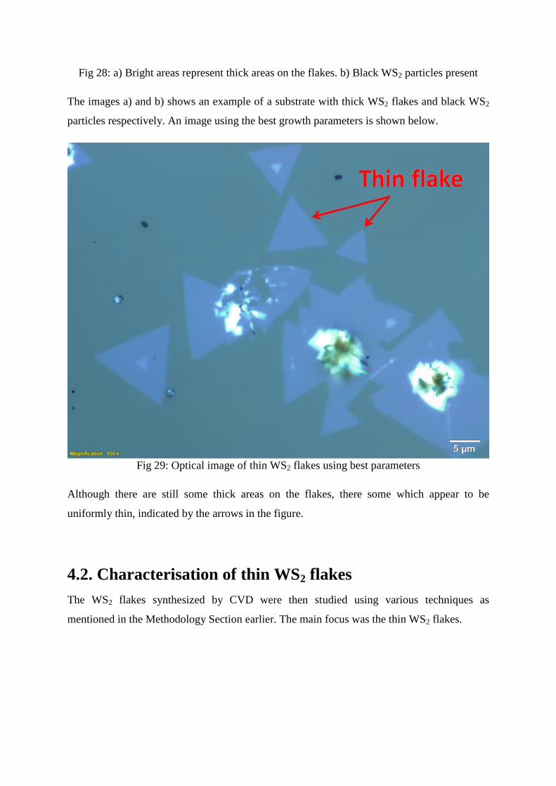
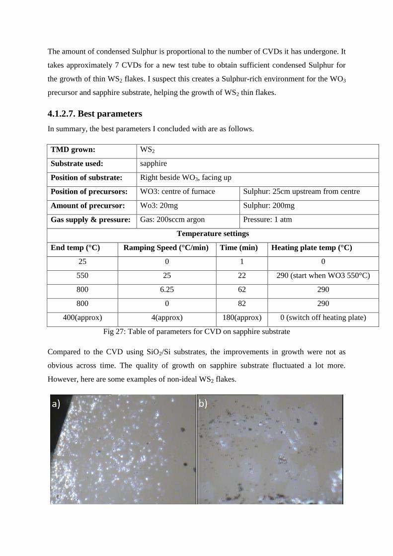
Fig 28: a) Bright areas represent thick areas on the flakes. b) Black WS2 particles present
The images a) and b) shows an example of a substrate with thick WS2 flakes and black WS2
particles respectively. An image using the best growth parameters is shown below.
Fig 29: Optical image of thin WS2 flakes using best parameters
Although there are still some thick areas on the flakes, there some which appear to be
uniformly thin, indicated by the arrows in the figure.
4.2. Characterisation of thin WS2 flakes
The WS2 flakes synthesized by CVD were then studied using various techniques as
mentioned in the Methodology Section earlier. The main focus was the thin WS2 flakes.
4.2.1. Raman Spectroscopy
Raman Spectroscopy was used mainly for identification of objects rather than the study of the
vibrational modes in the WS2 flake. The Raman Spectroscopy results for thin WS2 flakes on
both sapphire and SiO2/Si substrates are shown in the graphs below.
Fig 30: Raman Spectrum of WS2 flake on sapphire substrate
Fig 31: Raman Spectrum of WS2 flake on SiO2/Si substrate
It can be seen that the peaks obtained for both Raman spectrums are the same, except that the
spectrum taken on SiO2/Si substrate has an extra peak at 520cm-1
. According to Peimyoo et
al.10
, this 520cm-1
peak corresponds to a vibrational mode in the Silicon present in the
4000
6000
8000
10000
12000
14000
16000
250 300 350 400 450 500 550
Inte
nsi
ty (
a.u
.)
Raman Shift (cm-1)
Raman Spectrum of WS2 on Sapphire
0
5000
10000
15000
20000
25000
30000
35000
40000
250 300 350 400 450 500 550
Inte
nsi
ty (
a.u
.)
Raman Shift (cm-1)
Raman Spectrum of WS2 on SiO2/Si
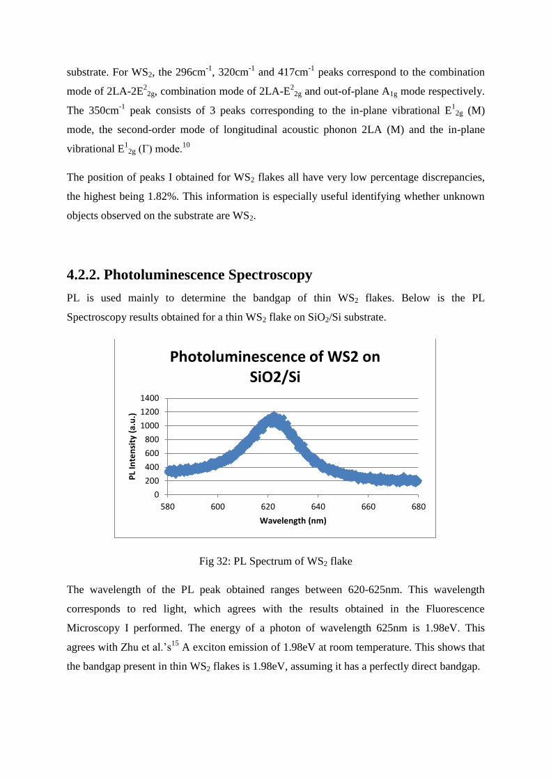
substrate. For WS2, the 296cm-1
, 320cm-1
and 417cm-1
peaks correspond to the combination
mode of 2LA-2E2
2g, combination mode of 2LA-E2
2g and out-of-plane A1g mode respectively.
The 350cm-1
peak consists of 3 peaks corresponding to the in-plane vibrational E1
2g (M)
mode, the second-order mode of longitudinal acoustic phonon 2LA (M) and the in-plane
vibrational E1
2g (Γ) mode.10
The position of peaks I obtained for WS2 flakes all have very low percentage discrepancies,
the highest being 1.82%. This information is especially useful identifying whether unknown
objects observed on the substrate are WS2.
4.2.2. Photoluminescence Spectroscopy
PL is used mainly to determine the bandgap of thin WS2 flakes. Below is the PL
Spectroscopy results obtained for a thin WS2 flake on SiO2/Si substrate.
Fig 32: PL Spectrum of WS2 flake
The wavelength of the PL peak obtained ranges between 620-625nm. This wavelength
corresponds to red light, which agrees with the results obtained in the Fluorescence
Microscopy I performed. The energy of a photon of wavelength 625nm is 1.98eV. This
agrees with Zhu et al.’s15
A exciton emission of 1.98eV at room temperature. This shows that
the bandgap present in thin WS2 flakes is 1.98eV, assuming it has a perfectly direct bandgap.
0
200
400
600
800
1000
1200
1400
580 600 620 640 660 680
PL
Inte
nsi
ty (
a.u
.)
Wavelength (nm)
Photoluminescence of WS2 on SiO2/Si
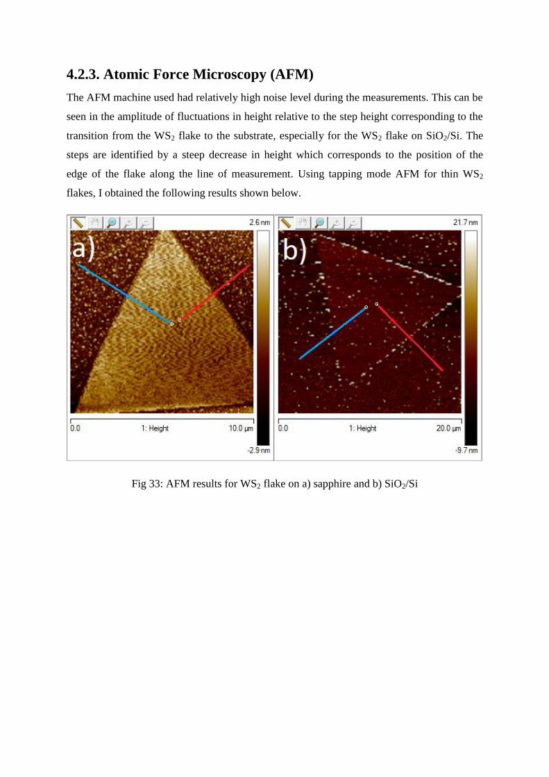
4.2.3. Atomic Force Microscopy (AFM)
The AFM machine used had relatively high noise level during the measurements. This can be
seen in the amplitude of fluctuations in height relative to the step height corresponding to the
transition from the WS2 flake to the substrate, especially for the WS2 flake on SiO2/Si. The
steps are identified by a steep decrease in height which corresponds to the position of the
edge of the flake along the line of measurement. Using tapping mode AFM for thin WS2
flakes, I obtained the following results shown below.
Fig 33: AFM results for WS2 flake on a) sapphire and b) SiO2/Si
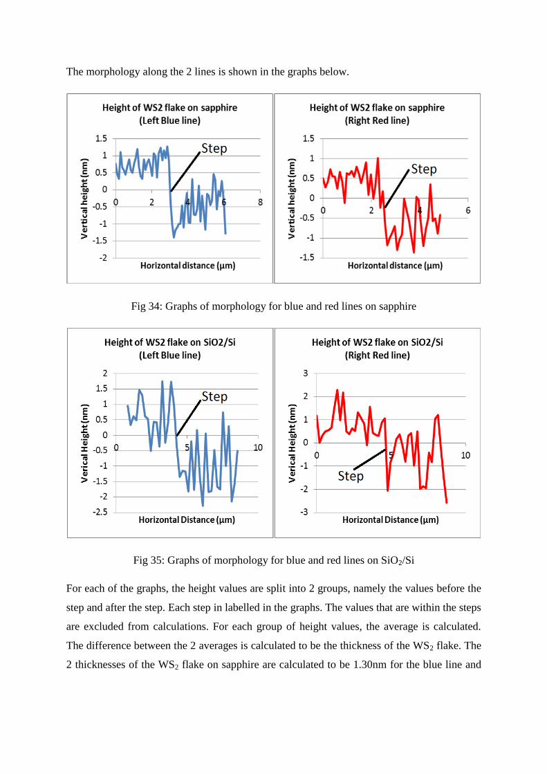
The morphology along the 2 lines is shown in the graphs below.
Fig 34: Graphs of morphology for blue and red lines on sapphire
Fig 35: Graphs of morphology for blue and red lines on SiO2/Si
For each of the graphs, the height values are split into 2 groups, namely the values before the
step and after the step. Each step in labelled in the graphs. The values that are within the steps
are excluded from calculations. For each group of height values, the average is calculated.
The difference between the 2 averages is calculated to be the thickness of the WS2 flake. The
2 thicknesses of the WS2 flake on sapphire are calculated to be 1.30nm for the blue line and
1.13nm for the red line. The 2 thicknesses for the WS2 flake on SiO2/Si are calculated to be
1.72nm for the blue line and 1.43nm for the red line.
The thickness of 1 layer of WS2 is approximately 0.7nm.10
With this knowledge, the WS2
flake on sapphire is 1-2 layers and the flake on SiO2/Si is 2-3 layers.
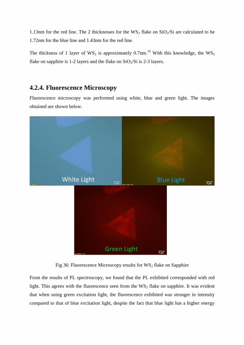
4.2.4. Fluorescence Microscopy
Fluorescence microscopy was performed using white, blue and green light. The images
obtained are shown below.
Fig 36: Fluorescence Microscopy results for WS2 flake on Sapphire
From the results of PL spectroscopy, we found that the PL exhibited corresponded with red
light. This agrees with the fluorescence seen from the WS2 flake on sapphire. It was evident
that when using green excitation light, the fluorescence exhibited was stronger in intensity
compared to that of blue excitation light, despite the fact that blue light has a higher energy
photon than green light. This shows that green light is closer to the excitation maximum than
blue light.
It can be seen that the fluorescence exhibited on the flake has a certain pattern. It is suspected
that this pattern reveals the grain boundaries present in the WS2 flake, which is not visible
under white light.
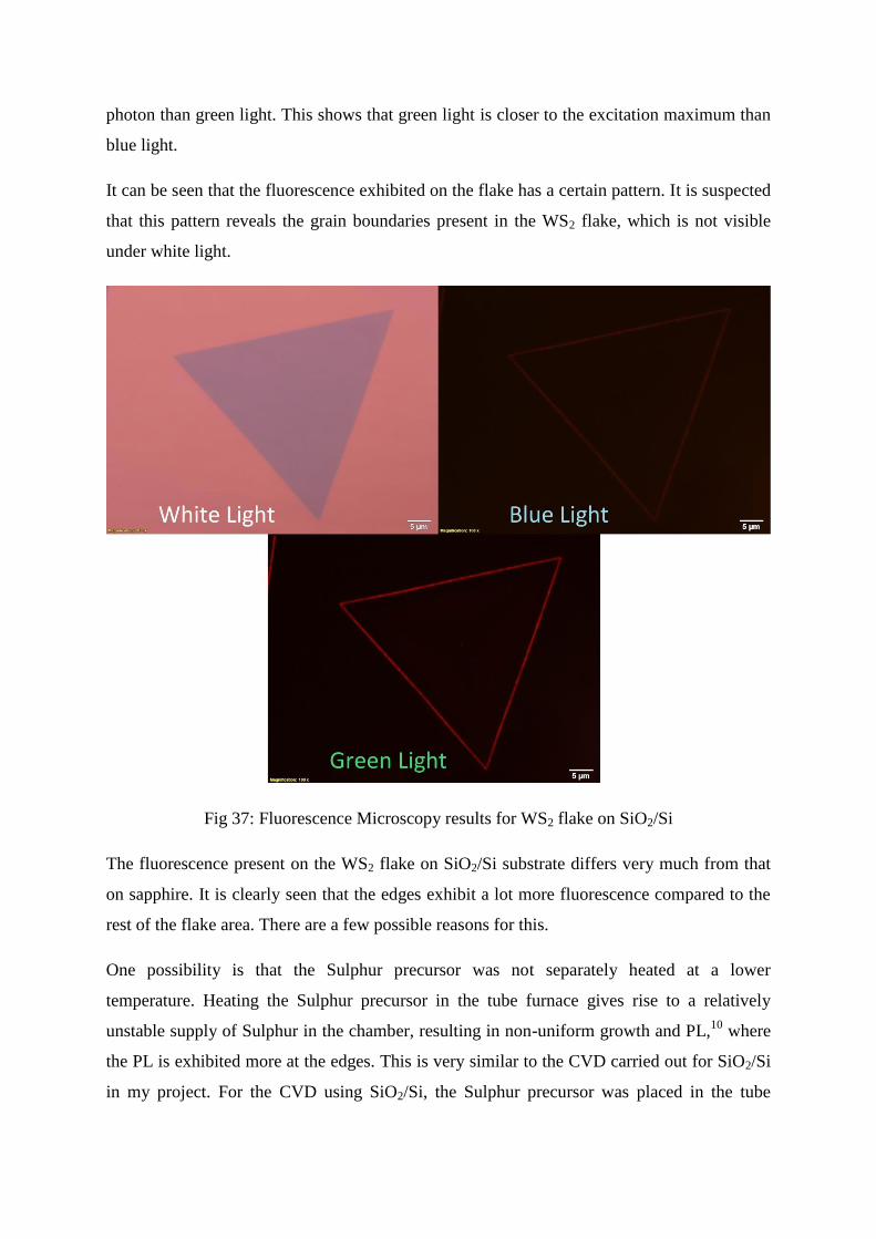
Fig 37: Fluorescence Microscopy results for WS2 flake on SiO2/Si
The fluorescence present on the WS2 flake on SiO2/Si substrate differs very much from that
on sapphire. It is clearly seen that the edges exhibit a lot more fluorescence compared to the
rest of the flake area. There are a few possible reasons for this.
One possibility is that the Sulphur precursor was not separately heated at a lower
temperature. Heating the Sulphur precursor in the tube furnace gives rise to a relatively
unstable supply of Sulphur in the chamber, resulting in non-uniform growth and PL,10
where
the PL is exhibited more at the edges. This is very similar to the CVD carried out for SiO2/Si
in my project. For the CVD using SiO2/Si, the Sulphur precursor was placed in the tube
furnace, whereas for the CVD using sapphire, the Sulphur precursor was heated at a constant
temperature outside the tube furnace.
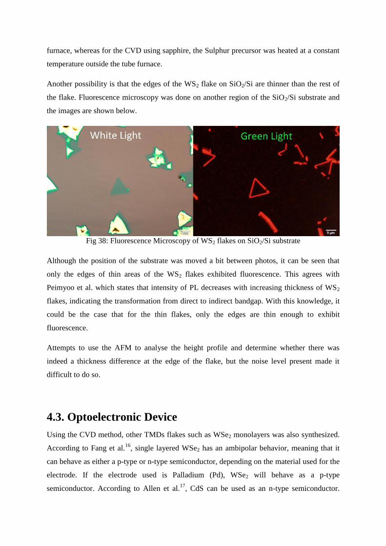
Another possibility is that the edges of the WS2 flake on SiO2/Si are thinner than the rest of
the flake. Fluorescence microscopy was done on another region of the SiO2/Si substrate and
the images are shown below.
Fig 38: Fluorescence Microscopy of WS2 flakes on SiO2/Si substrate
Although the position of the substrate was moved a bit between photos, it can be seen that
only the edges of thin areas of the WS2 flakes exhibited fluorescence. This agrees with
Peimyoo et al. which states that intensity of PL decreases with increasing thickness of WS2
flakes, indicating the transformation from direct to indirect bandgap. With this knowledge, it
could be the case that for the thin flakes, only the edges are thin enough to exhibit
fluorescence.
Attempts to use the AFM to analyse the height profile and determine whether there was
indeed a thickness difference at the edge of the flake, but the noise level present made it
difficult to do so.
4.3. Optoelectronic Device
Using the CVD method, other TMDs flakes such as WSe2 monolayers was also synthesized.
According to Fang et al.16
, single layered WSe2 has an ambipolar behavior, meaning that it
can behave as either a p-type or n-type semiconductor, depending on the material used for the
electrode. If the electrode used is Palladium (Pd), WSe2 will behave as a p-type
semiconductor. According to Allen et al.17
, CdS can be used as an n-type semiconductor.
According to Dong et al.18
, CdSe can also be used as an n-type semiconductor. According to
Baglio et al.19
, WS2 could be used as either p-type or n-type semiconductor. With this
knowledge, I wanted to construct a p-n junction using WSe2 and CdS0.8Se0.2.
Synthesizing WSe2 flakes on sapphire substrate uses the same CVD technique as that of WS2
flakes on sapphire. A heating plate was used to separately heat the Selenium precursor
outside the tube furnace. According to Liu et al.20
, the bandgap for monolayer WSe2 is
approximately 1.6eV, which corresponds to photons of 775nm wavelength, which is in the
infra-red spectrum.
An optoelectronic device was fabricated using a sapphire substrate with WSe2 flakes grown
on it and a CdS0.8Se0.2 nanowire. This optoelectronic device helps us to incorporate the WSe2
flake and CdS0.8Se0.2 nanowire into a circuit through the use of electrodes, while keeping the
WSe2 flake and CdS0.8Se0.2 nanowire exposed so that lasers can be incident onto it. This helps
in the study of the optoelectronic properties of the heterostructure junction between WSe2 and
CdS0.8Se0.2. This optoelectronic device is fabricated through the Electron Beam Lithography
(EBL) method.
For the measurements of IV graphs and Ivst graphs, different lasers of wavelengths 543nm
(green), 405nm (blue), and 660nm (red) were used separately. The power for all 3 lasers used
was 1.00mW with a spot size of approximately 2mm2.
4.3.1. IV graphs
The IV graphs were measured for dark current (with no laser incident upon it) and with lasers
of different wavelengths.
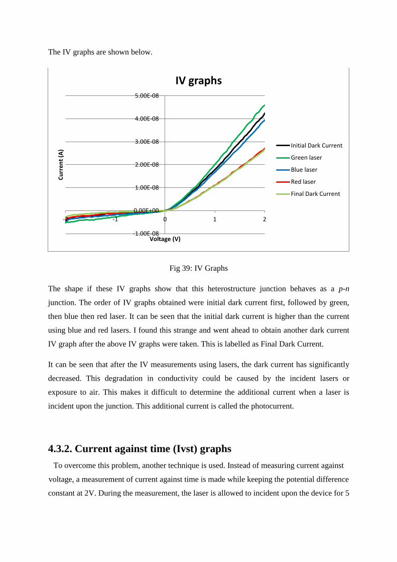
The IV graphs are shown below.
Fig 39: IV Graphs
The shape if these IV graphs show that this heterostructure junction behaves as a p-n
junction. The order of IV graphs obtained were initial dark current first, followed by green,
then blue then red laser. It can be seen that the initial dark current is higher than the current
using blue and red lasers. I found this strange and went ahead to obtain another dark current
IV graph after the above IV graphs were taken. This is labelled as Final Dark Current.
It can be seen that after the IV measurements using lasers, the dark current has significantly
decreased. This degradation in conductivity could be caused by the incident lasers or
exposure to air. This makes it difficult to determine the additional current when a laser is
incident upon the junction. This additional current is called the photocurrent.
4.3.2. Current against time (Ivst) graphs
To overcome this problem, another technique is used. Instead of measuring current against
voltage, a measurement of current against time is made while keeping the potential difference
constant at 2V. During the measurement, the laser is allowed to incident upon the device for 5
-1.00E-08
0.00E+00
1.00E-08
2.00E-08
3.00E-08
4.00E-08
5.00E-08
-2 -1 0 1 2
Cu
rre
nt
(A)
Voltage (V)
IV graphs
Initial Dark Current
Green laser
Blue laser
Red laser
Final Dark Current
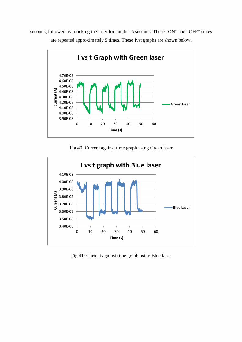
seconds, followed by blocking the laser for another 5 seconds. These “ON” and “OFF” states
are repeated approximately 5 times. These Ivst graphs are shown below.
Fig 40: Current against time graph using Green laser
Fig 41: Current against time graph using Blue laser
3.90E-08
4.00E-08
4.10E-08
4.20E-08
4.30E-08
4.40E-08
4.50E-08
4.60E-08
4.70E-08
0 10 20 30 40 50 60
Cu
rre
nt
(A)
Time (s)
I vs t Graph with Green laser
Green laser
3.40E-08
3.50E-08
3.60E-08
3.70E-08
3.80E-08
3.90E-08
4.00E-08
4.10E-08
0 10 20 30 40 50 60
Cu
rre
nt
(A)
Time (s)
I vs t graph with Blue laser
Blue Laser
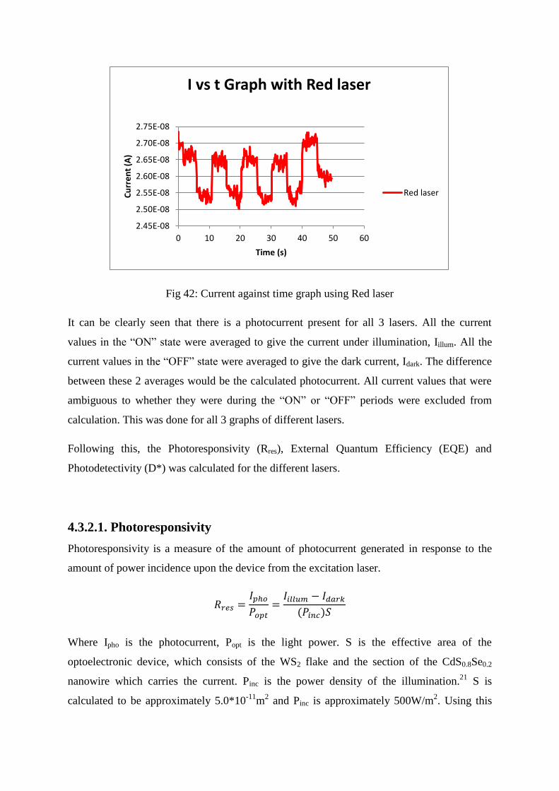
Fig 42: Current against time graph using Red laser
It can be clearly seen that there is a photocurrent present for all 3 lasers. All the current
values in the “ON” state were averaged to give the current under illumination, Iillum. All the
current values in the “OFF” state were averaged to give the dark current, Idark. The difference
between these 2 averages would be the calculated photocurrent. All current values that were
ambiguous to whether they were during the “ON” or “OFF” periods were excluded from
calculation. This was done for all 3 graphs of different lasers.
Following this, the Photoresponsivity (Rres), External Quantum Efficiency (EQE) and
Photodetectivity (D*) was calculated for the different lasers.
4.3.2.1. Photoresponsivity
Photoresponsivity is a measure of the amount of photocurrent generated in response to the
amount of power incidence upon the device from the excitation laser.
𝑅𝑟𝑒𝑠 =𝐼𝑝ℎ𝑜
𝑃𝑜𝑝𝑡=
𝐼𝑖𝑙𝑙𝑢𝑚 − 𝐼𝑑𝑎𝑟𝑘
(𝑃𝑖𝑛𝑐)𝑆
Where Ipho is the photocurrent, Popt is the light power. S is the effective area of the
optoelectronic device, which consists of the WS2 flake and the section of the CdS0.8Se0.2
nanowire which carries the current. Pinc is the power density of the illumination.21
S is
calculated to be approximately 5.0*10-11
m2 and Pinc is approximately 500W/m
2. Using this
2.45E-08
2.50E-08
2.55E-08
2.60E-08
2.65E-08
2.70E-08
2.75E-08
0 10 20 30 40 50 60
Cu
rre
nt
(A)
Time (s)
I vs t Graph with Red laser
Red laser
information, Rres was calculated to be 0.161AW-1
for green laser, 0.150AW-1
for blue laser
and 0.0442AW-1
for red laser.
A similar experiment was carried out by a senior student in NUS, where the electrodes were
placed on a single WSe2 flake on her device. A laser of wavelength 532nm was used for
global irradiation with a power of 2.8mW and a spot size of ~2mm2
. The photoresponsivity
calculated was 25mAW-1
. It can be seen that by adding a CdS0.8Se0.2 nanowire, the
heterostructure has enhanced the overall photoresponsivity compared to if just WSe2 was
used. These results are currently in the process of being published.
According to Kang et al.22
, the photoresponsivity of WSe2 was calculated to be
approximately 4.5mAW-1
when using a excitation wavelength of 785nm and power of 1mW.
Although the excitation wavelength used is not the same as the ones used in my project, this
photoresponsivity value supports that the use of heterostructure is probably better than non-
heterostructure.
4.3.2.2.External Quantum Efficiency
External Quantum Efficiency (EQE) shows the number of additional charge carriers
generated per photon that incidence upon the device. EQE is calculated using the equation
below.
𝐸𝑄𝐸 = ℎ𝑐𝑅𝑟𝑒𝑠
𝑒𝜆
Using the photoresponsivity, Rres, the EQE can be calculated. h is Planck’s constant, c is the
speed of light, e is the charge of an electron and λ is the excitation wavelength.23
The EQE
calculated is 0.492 for green laser, 0.458 for blue laser and 0.135 for red laser.
The EQE calculated from using a single WSe2 flake was 0.0583.
4.3.2.3. Photodetectivity
Photodetectivity is a measure of the performance of a photon sensitive device.
Photodetectivity is calculated using the equation below.22
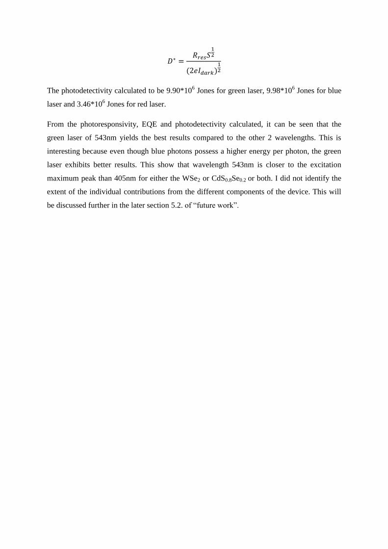
𝐷∗ =𝑅𝑟𝑒𝑠𝑆
12
(2𝑒𝐼𝑑𝑎𝑟𝑘)12
The photodetectivity calculated to be 9.90*106 Jones for green laser, 9.98*10
6 Jones for blue
laser and 3.46*106 Jones for red laser.
From the photoresponsivity, EQE and photodetectivity calculated, it can be seen that the
green laser of 543nm yields the best results compared to the other 2 wavelengths. This is
interesting because even though blue photons possess a higher energy per photon, the green
laser exhibits better results. This show that wavelength 543nm is closer to the excitation
maximum peak than 405nm for either the WSe2 or CdS0.8Se0.2 or both. I did not identify the
extent of the individual contributions from the different components of the device. This will
be discussed further in the later section 5.2. of “future work”.
5. Conclusion
5.1. Summary of project
In my project, I managed to synthesize thin WS2 flakes on sapphire and SiO2/Si substrates.
This was done by optimising the parameters for the Chemical Vapour Deposition process.
The parameters that were varied for the parameter search were the position of the substrate,
position and amount of precursor, temperature settings, gas supply rate, pressure and a few
others. The parameters used on SiO2/Si could also be used for Si3N4 substrate.
Next, the characteristics of the WS2 flakes were studied using different techniques. Raman
Spectroscopy was used for identification of WS2. Photoluminescence Spectroscopy was used
for determining the bandgap of WS2, which is approximately 1.98eV, corresponding to a
wavelength of 625nm. Atomic Force Microscopy was used to measure the morphology and
thickness of the WS2 flakes, where it was found that the WS2 flakes grown on sapphire
substrate were between 1-2 layers and the flakes on SiO2/Si substrate were between 2-3
layers. Fluorescence Microscopy is used to observe which areas on the WS2 flake exhibit
fluorescence. It was observed that WS2 flakes on sapphire substrate generally exhibited
fluorescence throughout its whole area, whereas the thin WS2 flake on SiO2/Si exhibited
fluorescence only at the edges.
Finally, with the use of a heterostructure optoelectronic device using a WSe2 flake and
CdS0.8Se0.2 nanowire , the current against voltage (IV) graphs and current against time (Ivst)
graphs were obtained using lasers of 3 different wavelengths. The Ivst measurements were
done for “ON” and “OFF” states where the laser was unblocked and blocked respectively.
Photoresponsivity, External Quantum Efficiency (EQE) and Photodetectivity were calculated
for each of the lasers. It can be seen that the excitation wavelength of 543nm was the closest
to the excitation maximum compared to 405nm and 660nm wavelengths for either WSe2 or
CdS0.8Se0.2. Cross referencing the Photoresponsivity of WSe2 flakes, the heterostructure
junction shows promising improvements in optoelectronics.
5.2. Possible Future Work
Due to time constrains, there are a few more things related to my project that can be explored
and studied in the future.
Instead of synthesizing the 2 materials of the heterostructure separately and then manually
stacking them, another suggestion is that a 2 step CVD process can be used synthesize the
heterostructure. This means that after synthesizing a TMD flake for example, the substrate
can be used for the synthesis of the next TMD, where the second TMD can possibly grow on
top of the first TMD. This might give rise to different or enhanced optoelectronic properties.
It was observed that only the edges of the thin WS2 flakes grown on SiO2/Si substrate
exhibited fluorescence whereas the other areas exhibited much less. More research can be
done on this. A more accurate AFM with less noise can be used to measure a very detailed
height profile at the edge of the flake to see if indeed the edge is thinner than the rest of the
flake.
It was found that the heterostructure junction exhibits photocurrent when exposed to lasers.
However, global irradiation was used, which means that the extent of photocurrent
contributions from the different components on the device is unknown. Instead of using a
broad beam laser, a focused laser can be used to irradiate only specific components on the
optoelectronic device. This way, the contributions photocurrent from each component can be
determined.
To expand on my findings, another identical optoelectronic device can be constructed, except
that instead of having heterostructure junction of WSe2 and CdS0.8Se0.2, only WSe2 is used.
This way, a direct comparison can be done between using a single material and a
heterostructure junction, performing the exact measurements on each device.
Different combinations of heterostructures can be used too. There are other TMDs available
such as MoS2 and MoSe2. CdS and CdSe can also be used instead of CdSxSe1-x.
References:
1) Meric, I., Baklitskaya, N., Kim, P., & Shepard, K. L. (2008, December). RF
performance of top-gated, zero-bandgap graphene field-effect transistors. InIEEE
International Electron Devices Meeting (pp. 1-4).
2) Dean, C. R., Young, A. F., Meric, I., Lee, C., Wang, L., Sorgenfrei, S., ... & Hone, J.
(2010). Boron nitride substrates for high-quality graphene electronics.Nature
nanotechnology, 5(10), 722-726.
3) Yun, W. S., Han, S. W., Hong, S. C., Kim, I. G., & Lee, J. D. (2012). Thickness and
strain effects on electronic structures of transition metal dichalcogenides: 2H-M X 2
semiconductors (M= Mo, W; X= S, Se, Te).Physical Review B, 85(3), 033305.
4) Eda, G., Yamaguchi, H., Voiry, D., Fujita, T., Chen, M., & Chhowalla, M. (2011).
Photoluminescence from chemically exfoliated MoS2. Nano letters,11(12), 5111-
5116.
5) Mueller, T., Furchi, M. M., Pospischil, A., & Polyushkin, D. K. (2014, December).
Nanophotonics with two-dimensional atomic crystals. In Electron Devices Meeting
(IEDM), 2014 IEEE International (pp. 5-5). IEEE.
6) Tongay, S., Zhou, J., Ataca, C., Lo, K., Matthews, T. S., Li, J., ... & Wu, J. (2012).
Thermally driven crossover from indirect toward direct bandgap in 2D
semiconductors: MoSe2 versus MoS2. Nano letters, 12(11), 5576-5580.
7) Chhowalla, M., Shin, H. S., Eda, G., Li, L. J., Loh, K. P., & Zhang, H. (2013). The
chemistry of two-dimensional layered transition metal dichalcogenide
nanosheets. Nature chemistry, 5(4), 263-275.
8) Ling, X., Lee, Y. H., Lin, Y., Fang, W., Yu, L., Dresselhaus, M. S., & Kong, J.
(2014). Role of the seeding promoter in MoS2 growth by chemical vapor
deposition. Nano letters, 14(2), 464-472.
9) Lee, Y. H., Zhang, X. Q., Zhang, W., Chang, M. T., Lin, C. T., Chang, K. D., ... &
Lin, T. W. (2012). Synthesis of Large‐Area MoS2 Atomic Layers with Chemical
Vapor Deposition. Advanced Materials, 24(17), 2320-2325.
10) Peimyoo, N., Shang, J., Cong, C., Shen, X., Wu, X., Yeow, E. K., & Yu, T. (2013).
Nonblinking, intense two-dimensional light emitter: Monolayer WS2 triangles. ACS
nano, 7(12), 10985-10994.
11) Gfroerer, T. H. (2000). Photoluminescence in analysis of surfaces and
interfaces. Encyclopedia of Analytical Chemistry.
12) Choi, J. O., Moore, J. A., Corelli, J. C., Silverman, J. P., & Bakhru, H. (1988).
Degradation of poly (methylmethacrylate) by deep ultraviolet, x‐ray, electron beam,
and proton beam irradiations. Journal of Vacuum Science & Technology B, 6(6),
2286-2289.
13) Junpeng, L., Cheng, S., Minrui, Z., Mathews, N., Hongwei, L., Gin Seng, C., ... &
Chorng Haur, S. (2011). Facile One-Step Synthesis of CdS x Se1–x Nanobelts with
Uniform and Controllable Stoichiometry. The Journal of Physical Chemistry
C, 115(40), 19538-19545.
14) Rong, Y., Fan, Y., Koh, A. L., Robertson, A. W., He, K., Wang, S., ... & Warner, J.
H. (2014). Controlling sulphur precursor addition for large single crystal domains of
WS 2. Nanoscale, 6(20), 12096-12103.
15) Zhu, B., Zeng, H., Dai, J., Gong, Z., & Cui, X. (2014). Anomalously robust valley
polarization and valley coherence in bilayer WS2. Proceedings of the National
Academy of Sciences, 111(32), 11606-11611.
16) Fang, H., Chuang, S., Chang, T. C., Takei, K., Takahashi, T., & Javey, A. (2012).
High-performance single layered WSe2 p-FETs with chemically doped
contacts. Nano letters, 12(7), 3788-3792.
17) Bard, A. J., & Wrighton, M. S. (1977). Thermodynamic Potential for the Anodic
Dissolution of n‐Type Semiconductors A Crucial Factor Controlling Durability and
Efficiency in Photoelectrochemical Cells and an Important Criterion in the Selection
of New Electrode/Electrolyte Systems. Journal of the Electrochemical
Society, 124(11), 1706-1710.
18) Yu, D., Wang, C., & Guyot-Sionnest, P. (2003). n-Type conducting CdSe nanocrystal
solids. Science, 300(5623), 1277-1280.
19) Baglio, J. A., Calabrese, G. S., Harrison, D. J., Kamieniecki, E., Ricco, A. J.,
Wrighton, M. S., & Zoski, G. D. (1983). Electrochemical characterization of p-type
semiconducting tungsten disulfide photocathodes: efficient photoreduction processes
at semiconductor/liquid electrolyte interfaces. Journal of the American Chemical
Society, 105(8), 2246-2256.
20) Liu, W., Kang, J., Sarkar, D., Khatami, Y., Jena, D., & Banerjee, K. (2013). Role of
metal contacts in designing high-performance monolayer n-type WSe2 field effect
transistors. Nano letters, 13(5), 1983-1990.
21) Lu, J.P., Liu, H., Deng, S., Zheng, M., Wang, Y., Kan, J.A.V., Sing, H.T., Zhang, X.,
Chorng, H.S., Subodh, G.M. (2014). Highly sensitive and multispectral responsive
phototransistor using tungsten-doped VO2 nanowires. Nanoscale, 6,7619-7627
22) Kang, D. H., Shim, J., Jang, S. K., Jeon, J., Jeon, M. H., Yeom, G. Y., ... & Park, J. H.
(2015). Controllable Nondegenerate p-Type Doping of Tungsten Diselenide by
Octadecyltrichlorosilane. ACS nano, 9(2), 1099-1107.
23) Baugher, B. W., Churchill, H. O., Yang, Y., & Jarillo-Herrero, P. (2014).
Optoelectronic devices based on electrically tunable pn diodes in a monolayer
dichalcogenide. Nature nanotechnology, 9(4), 262-267.