28nm Generation Programmable Families - Hot Chips · ADC TxA TxB sRX ADC ADC RxA RxB Control To...
25
August 8, 2010 28nm Generation Programmable Families 7 Series FPGAs Extensible Processing Platform Family AMBA AXI4 IP Brad Taylor Ralph Wittig
Transcript of 28nm Generation Programmable Families - Hot Chips · ADC TxA TxB sRX ADC ADC RxA RxB Control To...

August 8, 2010
28nm Generation Programmable Families7 Series FPGAsExtensible Processing Platform FamilyAMBA AXI4 IP
Brad TaylorRalph Wittig

Xilinx Public
Enhanced IO Bandwidth
Xilinx 7 Series 28 nm Families
Enhanced Power Efficiency
Agenda
Page 2
Enhanced Logic Density
Extensible Processing Platform
Advanced Interconnect System

Xilinx Public
Xilinx 28nm High Performance Low Power Process
28nm process node First wave of 28nm HK/MG devices from fabless Si vendors >2x device capacity over 40nm devices ~50% total power reduction over 40nm devices
Xilinx 28nm High -Performance, Low -Power process High-K Metal Gate (HK/MG) Developed by Xilinx and TSMC - optimized for high performance & low power 65% lower static power than 28nm variants offering similar performance
Page 3
Process Xilinx 40nm High Performance
28nm LowPower
28nm HighPerformance
28nm High PerformanceLow Power
Gate Scheme SiON/Poly SiON/Poly HK/MG HK/MG
VCC 1V 1.05V .85V 1V
Static Power >2.5x 1.5x 2x 1.0x
FPGA Performance 1.0x 0.9x 1.02x 1.0x
* Estimation of FPGA performance based on Xilinx internal benchmark suite
*

Xilinx Public
Xilinx 28nm Total Power Reduction
Page 4
1) Total Power reduction estimated from Xilinx internal benchmarks (Range 45%-61%)2) Static power reduction for max VCC, 100 DegC, worst case process
New for 28nm – 50% Total Power Reduction from 40 nm– Static Power - 65% reduction
• Xilinx High Performance Low Power Process
– Dynamic Power – 25% reduction• 40nm => 28nm process shrink
– IO Power – 30% reduction• VCCAUX voltage reduction from 2.5V to 1.8V
• High Speed Transceiver power saving features
• Single Ended IO (DDR3) power saving features
• Support for 1.2V, 1.35V for memory standards
Activity Based Logic Optimization – 20% reduction– Available in ISE v12
– Average 20% savings (benchmark results)
– Leverages clock gating built into Logic Slice
Additional Low Power Device Options – -1L low power .9V speed grades - 20% power reduction
Xilinx Public
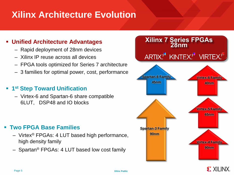
Xilinx Architecture Evolution
Unified Architecture Advantages– Rapid deployment of 28nm devices– Xilinx IP reuse across all devices– FPGA tools optimized for Series 7 architecture– 3 families for optimal power, cost, performance
Page 5
Virtex -5 Family
65nm
Spartan -3 Family
90nm
Virtex -4 Family
90nm
Virtex -6 Family
40nm
Spartan -6 Family
45nm
1st Step Toward Unification– Virtex-6 and Spartan-6 share compatible
6LUT, DSP48 and IO blocks
Two FPGA Base Families– Virtex® FPGAs: 4 LUT based high performance,
high density family
– Spartan® FPGAs: 4 LUT based low cost family

Xilinx Public
Unified FPGA Family Architecture
Series 7 Family Artix Kintex Virtex
MarketLowest Power
& Cost Best Price/PerformanceHighest System
PerformanceLogic Cells 20K - 355K 30K - 410K 285K - 2,000K
Memory Kbits 720 - 12,060 Kbits 2,340 - 28,620 Kbits 14,760 - 64,800 Kbits DSP Slices 40 - 700 120-1,540 700 - 3,960
Max Transceivers 3.75 Gbps6.6 Gbps
10.3 Gbps
10.3 Gbps 13.1 Gbps 28.0 Gbps
External Memory Performance 800 Mbps 2,133 Mbps 2,133 MbpsMax Select IO 450 500 1200
Select IO Voltages 3.3V and below3.3V and below1.8V and below
3.3V and below1.8V and below
Relative Static Power .5x 1.0x 1.0x Relative Performance .65x 1.0x 1.0x
Page 6

Xilinx Public
65nm 40/45nm 28nm
200K
400K
600K
Logic Cells
800K
1,000K
332K
150K
760K
355K410K
More than Moore
Challenge:– Frequency scaling is minimal
– Performance gains focused on parallelism (= capacity)
– Moore’s Law only doubles capacity
Solution:– New packaging & assembly methodology
Result:> 2x capacity gains over 40nm devices
Page 7
Virt
ex-7
Virt
ex-6
Spartan -6V
irtex
-5
Dramatic Capacity Increases
Art
ix-7
Family Capacity Range
Artix-7 20K – 355K LCs
Kintex-7 30K – 410K LCs
Virtex-7 285K – 2,000K LCs
2,000K
Kin
tex
-7
Xilinx Public
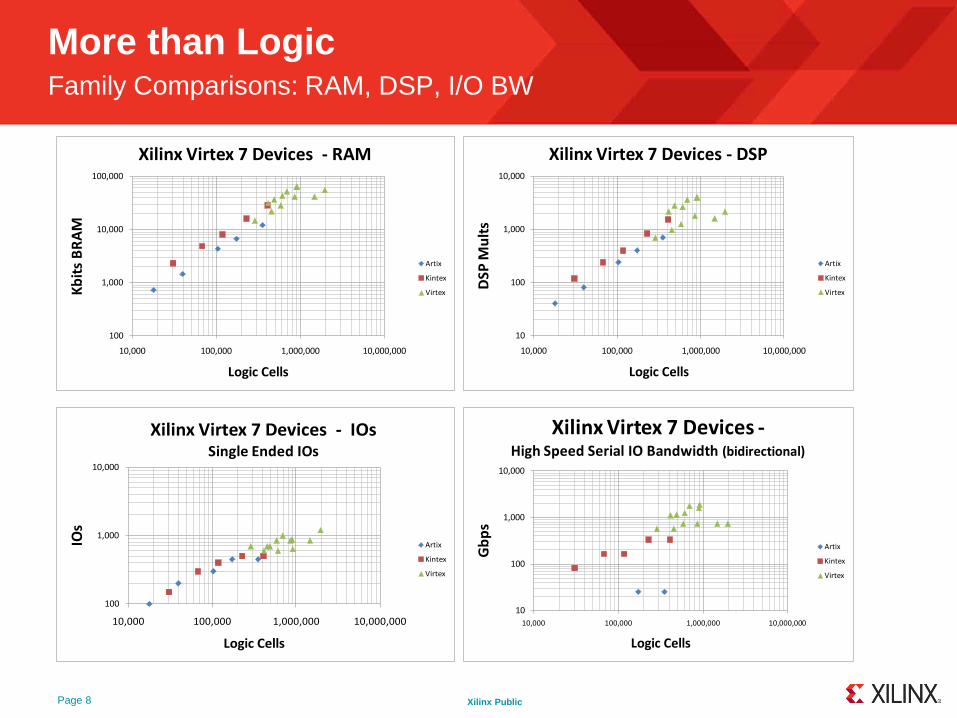
More than Logic Family Comparisons: RAM, DSP, I/O BW
Page 8
10
100
1,000
10,000
10,000 100,000 1,000,000 10,000,000
DS
P M
ult
s
Logic Cells
Xilinx Virtex 7 Devices - DSP
Artix
Kintex
Virtex
100
1,000
10,000
10,000 100,000 1,000,000 10,000,000
IOs
Logic Cells
Xilinx Virtex 7 Devices - IOs Single Ended IOs
Artix
Kintex
Virtex
100
1,000
10,000
100,000
10,000 100,000 1,000,000 10,000,000
Kb
its
BR
AM
Logic Cells
Xilinx Virtex 7 Devices - RAM
Artix
Kintex
Virtex
10
100
1,000
10,000
10,000 100,000 1,000,000 10,000,000
Gb
ps
Logic Cells
Xilinx Virtex 7 Devices -High Speed Serial IO Bandwidth (bidirectional)
Artix
Kintex
Virtex

Xilinx Public
High -Speed Transceiver Evolution
Page 9
GTP
GTP
GTX
GTH
6.6 Gbps
10.3125 Gbps
3.125 Gbps
11.18 Gbps
13.1 Gbps
3.75 Gbps
Virtex-6
Artix™-7
Kintex™-7 &Virtex™-7 T
Virtex™-7 X
Spartan-6
GTH
GTX
6 Series 7 Series
28Gbps *Transceivers
Challenge:– Increase device BW
– No increase in total device power
– XCVR gains from scaling: negligible
Solution:– Careful circuit design throughout XCVR
– Increased Gbps / XCVR
– More XCVR / Device
– Low power mode for short channels
– Lanes share a PLL vs PLL per lane
Result:– 60% Increased max device BW
– Device XCVR power unchanged
New 7-Series Family
GTP GTX GTH GT28
Max Rate (Gbps) 3.75 10.3125 13.1 28
Relative Power (Per GT) .35x .7x 1x -
Max GTs per Device 4 56 72 -
Tran
scei
ver
Rat
e (G
bps)
Xilinx Public
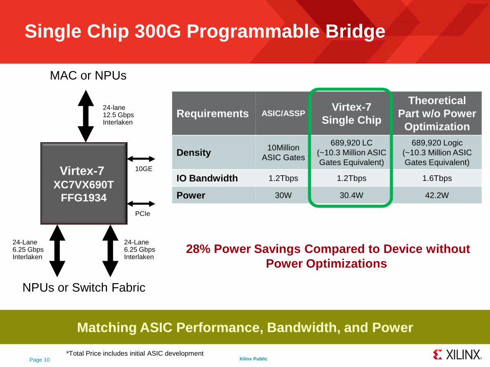
Single Chip 300G Programmable Bridge
Matching ASIC Performance, Bandwidth, and Power
Virtex -7 XC7VX690T
FFG1934
24-lane12.5 GbpsInterlaken
24-Lane6.25 GbpsInterlaken
24-Lane6.25 GbpsInterlaken
10GE
PCIe
MAC or NPUs
NPUs or Switch Fabric
Requirements ASIC/ASSPVirtex-7
Single Chip
Theoretical Part w/o Power
Optimization
Density 10Million ASIC Gates
689,920 LC(~10.3 Million ASIC Gates Equivalent)
689,920 Logic(~10.3 Million ASIC Gates Equivalent)
IO Bandwidth 1.2Tbps 1.2Tbps 1.6Tbps
Power 30W 30.4W 42.2W
*Total Price includes initial ASIC development
28% Power Savings Compared to Device withoutPower Optimizations
Page 10

Xilinx Public
Logic Cells
DSP Slices
Max. Transceivers
Transceivers Performance
Memory Performance
Max. SelectIO™
Select IO Voltages
Industry’s Best Price-Performance
Kintex -7Balancing Price/Performance
Page 11
Challenge– Cost sensitive mid range market segment
– No compromise in fabric performance
Solution– Same process as Virtex-7
Same Performance (as Virtex-7)
– Bare die flip chip packages
50% reduced cost (vs Virtex-6)
Trade Offs– Restricted max die size
– Reduced max XVER rate

Xilinx Public
Real World Customer Impact
Page 12
2x2 LTE RadioProcessor
CPRI/OBSAIMASTER
Memory
CPRI/OBSAISLAVE
Micro Interface
Memory Interface
SPI
DAC
DAC
ADC
TxA
TxB
sRX
ADC
ADC
RxA
RxB
ControlTo ASSPs
DAC’s, ADC’s& Synths (3v3)
SerDes
SerDes
DUC
DUC
DDC
DDC
PC-CFR
PC-CFR
DPD
DPD
SFP/SFP+
Connectors
Processor
CPRI/OBSAIMASTER
Memory
CPRI/OBSAISLAVE
Micro Interface
Memory Interface
SPI
DAC
DAC
ADC
TxA
TxB
sRX
ADC
ADC
RxA
RxB
ControlTo ASSPs
DAC’s, ADC’s& Synths (3v3)
SerDes
SerDes
DUC
DUC
DDC
DDC
PC-CFR
PC-CFR
DPD
DPD
SFP/SFP+
Connectors
2x2 LTE Radio
Virtex -6 LX75T Kintex -7 XC7K70T
RequirementsVirtex-6
LX75T-FF784Kintex-7
K70T-FBG676
FPGA Cost 1.0 .5
Sys Performance 368MHz 368MHz
Power 8.7W 4.48W
48% lower
power
2Xbetter
price /
performance
Kintex-7 Performance Upgradable to 491MHz

Xilinx Public
Availability
Page 13Page 13
First 28nm ES
201220112010
28nm Early Access Program
First 28nmProduction
2013
Note: Subject to change
28nm Family Rollout
28nm Design Kit Rollout
Tools available now
First devices in early 2011
Solution kits phasing in in late 2011

Xilinx Public
Xilinx EPP
Hybrid SOC + FPGA creates a new product class– Unprecedented configuration compared to an SOC
– Unprecedented integration compared to an FPGA
28nm based product
Significant advantages over a discrete uP + an FPGA – Cost, power, bandwidth and latency
Leverages best of ARM and Xilinx Ecosystem– Rich ecosystem of OS, Middleware and Tools support for ARM
– Tools and IP support for Xilinx FPGA
Today: EPP Overview
Future: Detailed family charts, performance numbers, etc
Page 14

Xilinx Public
EPP: An SOC from Xilinx(Coming from an FPGA company?)
An SOC with an embedded FPGA
Application level Dual Core ARM A9
Hard Peripherals
Cache and Memory
ASIC-like Cost
ASIC-like Power
+ 7 Series Programmable Logic
MemoryInterfaces
CommonPeripherals
ProcessorSystem
ARM®
Dual Cortex™ -A9MPCoreComplex
High -BandwidthAMBA ®-AXI Interfaces
ProgrammableLogic (PL)
Can you find the FPGA?
Boots like a Processor
Acts like a Processor
Really … is a Processor
… and more
Page 15

Xilinx Public
EPP: Extensible(the FPGA value add)
Extensible I/O Interfaces– Augment the built-in peripheral set
– Pre-designed standard peripherals
– User designed custom peripherals
High BW Real Time Processing– Video pipelines
– Low latency, real time events
CPU Offload (accelerators)– Xilinx XtremeDSP functions
– Custom processing functions
– Up to 0.2 T MAC/s, Up to 2.8 T (int16)
CPU Power Offload – ~10x power reduction per operation
Hybrid Many Core– Sea of custom processors in PL*
– OpenCL like machine
Page 16
Change the program
Customize I/O interfaces
Add compute accelerators
High -BandwidthAMBA ®-AXI Interfaces
ProgrammableLogic (PL)
Common Peripherals
CustomPeripherals
Common Accelerators
Custom Accelerators
ProcessorSystem
*PL = Programmable Logic
Xilinx Public
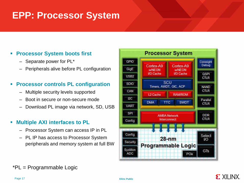
EPP: Processor System
Processor System boots first– Separate power for PL*
– Peripherals alive before PL configuration
Processor controls PL configuration– Multiple security levels supported
– Boot in secure or non-secure mode
– Download PL image via network, SD, USB
Multiple AXI interfaces to PL– Processor System can access IP in PL
– PL IP has access to Processor System peripherals and memory system at full BW
Page 17
*PL = Programmable Logic

Xilinx Public
EPP: Programming
Out-of -the-box SW programmable– No FPGA design expertise required
Standard OS support– Dual core ARM A9 base platform
Many Sources of SW and HW IP– Standardized around AMBA-AXI
– Xilinx, ARM libraries
– 3rd Parties
Industry -Leading Tools– ARM RVDS Suite & Ecosystem
– Open source GNU tools
– Xilinx ISE® Design Suite
– Xilinx Targeted Design Platforms
Programming
Integrate IP
Test
Release
Debug
Design
Xilinx IP
Partner IP
Custom IP
Integrate IP
Test
Release
Debug
Software Architect
Hardware Architect
SystemArchitect
Page 18

Xilinx Public
Customer Requests
Lessons Learned
Past Experience (8 Years) Xilinx EPP Solution
Processor-centric approach Software-centric approach ARM® processing engine AXI interface standard MicroBlaze continues as soft
core solution
MicroBlaze and PowerPC Processor IP and HW Tools FPGA design centric
Out-of-box programmable CPU architecture roadmap Open standards Ecosystem Scalable performance
ARM®, AMBA® are Registered Trademarks of ARM Ltd. PowerPC is a Register Trademark of IBMMicroBlaze® is a Registered Trademark of Xilinx
Page 19
Xilinx Public
AMBA AXI(New interconnect standard for all Xilinx IP)
Open standard from ARM– Well supported, documented and widely adopted– Broad set of IP available with AXI interface– Royalty free on any target technology
High performance interface– Optimized for frequency, throughput, latency and/or area – Supports pipelining with optional register slice– QoS controls
Easy to use– One family of interfaces to learn – Supports embedded, DSP, and logic users
Ecosystem– Partners are embracing Xilinx’ move to AXI– Verification IP available– Widely adopted in the ASIC world
New AXI4 interface variants optimal for FPGA– Xilinx contributed to specification process
Page 20

Xilinx Public
AXI Interconnect Usage
AXI4 interface variants optimized for area and performance AXI4: Maximizes data throughput for an interface
AXI4-Lite : Area efficient implementation, used for control and status
AXI4-Stream : Easily connect to non-address based peripherals
AXI4
AXI4
Stream
AXI4 LiteAXI4
AXI4 Lite
Processor System
IP Block
DMA
IP Block
IP Block
AXI Interconnect
Block
AXI4
Page 21

Xilinx PublicPage 22
AXI4 Transaction Examples
AXI4
Master Slave
Write Data
A0 A1 A2 A3 B0 B1 B2 B3 C0 C1
WLAST
WLAST marks packets (omit for continuous stream)
Streaming AXI
Channel payload
READY/VALID Handshake
AXI4 Base Protocol– Independent read and write interfaces
– Split transaction
• Address xfer decoupled from data xfer
– Simple READY/VALID handshake
– Data width from 8 to 1024 bits
– Burst size from 1-256 data beats
– Pipelined operation
• ID tags on each channel
• Overlapping transactions (reads/writes)
• Out-of-order completion (reads)
• Interleaving of data beats (reads)
AXI4-Lite– Single Transaction only (no burst)
AXI4-Stream– Write Data Channel only

Xilinx Public
AXI Interconnect IP(designed by Xilinx, optimized for FPGA)
Crossbar– Up to 16 masters and 16 slaves per interconnect
– Cascadeable (multi layer switches)
– Independent write and read address arbitration
– Sparse crossbar data path between configured endpoints
Data width, protocol and clock conversion– 32 to 1024 bit data width (256 bit max at launch)
– Built-in AXI4-Lite and AXI3 protocol conversion
– Asynchronous and integer-ratio clock conversion
Built -in buffering– Pipeline registers per channel to boost frequency
– Data FIFOs per endpoint for “bursty” throughput
Multiple threads (transaction IDs)– Read data reordering and interleaving between threads
– Reduces stalling
1-16 AXI slaves
1-16 AXI masters
.
.
.
.
.
.
Optional AXI Protocol Conversion • Data Width conversion• Protocol Bridge • Integer-Ratio Clock Bridge• Asynchronous Clock Bridge
Optional AXI Register Slice/Buffer• Configurable FIFO depth
axi_interconnect
Page 23

Xilinx PublicPage 24
Summary
Unified device architecture for all 7 Series FPGAs– Scalable platform with three families: cost, power, performance
– 50% total power reduction
– Increased capacity and bandwidth
Xilinx EPP: SOC with embedded programmable logic array– Boots like a processor
– SW centric programming model
– Extensible peripheral set and compute
All Xilinx IP (soft and hard) use AMBA AXI interconnect– High performance, scalable interconnect
– AXI4 is optimized for FPGAs
– Memory mapped and streaming interfaces
Availability– IP with AXI interface: Sept 2010
– 7 Series FPGAs: First devices in early 2011
– EPP: To Be Announced
Design GreenDesign Green by XilinxDesign GreenDesign Green by Xilinx

Xilinx Public
References
Xilinx 28 nm HPL technology– http://www.xilinx.com/support/documentation/white_papers/wp312_Next_Gen_28_nm_Overview.pdf
Xilinx Series 7 FPGA Families– http://www.xilinx.com/technology/roadmap/7-series-fpgas.htm
– Series 7 Press Backgrounder
Xilinx Extensible Processing Platform– http://www.xilinx.com/technology/roadmap/processing-platform.htm
– http://www.xilinx.com/publications/archives/xcell/issue71/cover-story.pdf
AMBA -AXI – http://www.arm.com/products/system-ip/amba/amba-open-specifications.php
Page 25