28nm FD-SOI RF and Analog 03102016 - mycmp.fr · Agenda • In the context of IoT • ST 28nm UTBB...
57
Technology Advantages for Analog/RF & Mixed-Signal Designs Philippe Cathelin, Andreia Cathelin STMicroelectronics, Crolles, France October 5, 2016 CMP 28FDSOI Training
Transcript of 28nm FD-SOI RF and Analog 03102016 - mycmp.fr · Agenda • In the context of IoT • ST 28nm UTBB...

TechnologyAdvantages for Analog/RF & Mixed-Signal Designs
Philippe Cathelin, Andreia Cathelin
STMicroelectronics, Crolles, France
October 5, 2016
CMP 28FDSOI Training
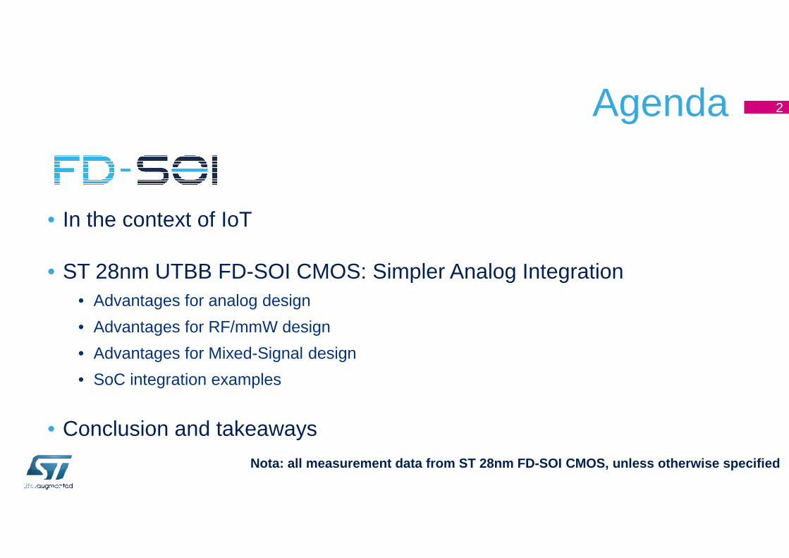
Agenda
• In the context of IoT
• ST 28nm UTBB FD-SOI CMOS: Simpler Analog Integration
2
• ST 28nm UTBB FD-SOI CMOS: Simpler Analog Integration• Advantages for analog design
• Advantages for RF/mmW design
• Advantages for Mixed-Signal design
• SoC integration examples
• Conclusion and takeaways
Nota: all measurement data from ST 28nm FD-SOI CMOS, unless otherwise specified

IoT Strategic Focus 3
SmartIndustry
SmartCity
SmartThings
The leading provider of products and solutions for the Internet of Things
SmartHome
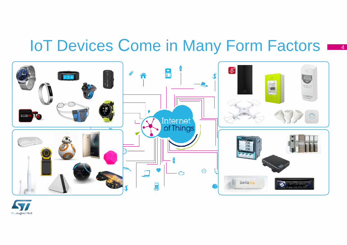
IoT Devices Come in Many Form Factors 4
ConnectivitySignal Conditioning
& Protection
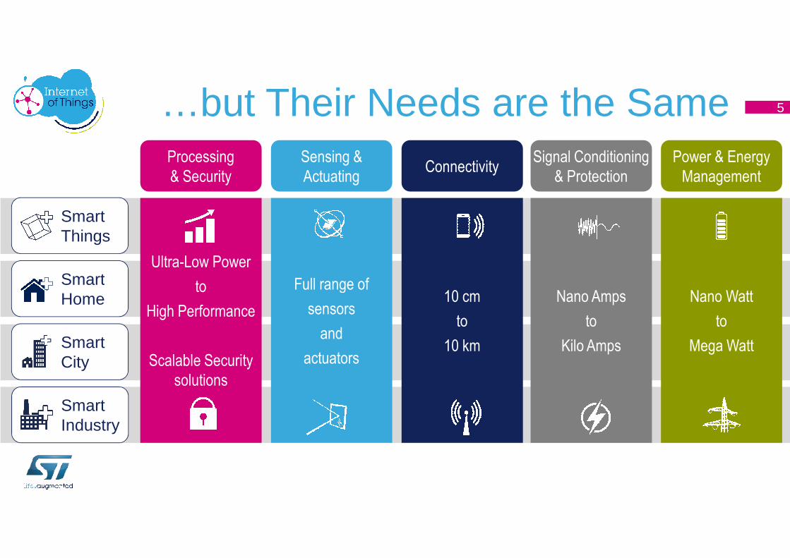
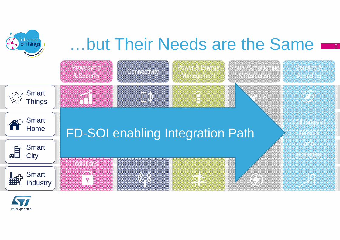
…but Their Needs are the Same 5
Sensing &
Actuating
Power & Energy
Management
SmartThings
Smart Full range of
Processing
& Security
Ultra-Low Power
to10 cm
to
10 km
Nano Amps
to
Kilo Amps
SmartIndustry
SmartCity
SmartHome
Full range of
sensors
and
actuators
Nano Watt
to
Mega Watt
to
High Performance
Scalable Security
solutions
…but Their Needs are the Same 6
SmartThings
Smart
Power & Energy
Management
Signal Conditioning
& Protection
Sensing &
Actuating
Full range of
ConnectivityProcessing
& Security
Ultra-Low Power
to
SmartIndustry
SmartCity
SmartHome Nano Watt
to
Mega Watt
Nano Amps
to
Kilo Amps
Full range of
sensors
and
actuators
10 cm
to
10 km
to
High Performance
Scalable Security
solutions
FD-SOI enabling Integration Path
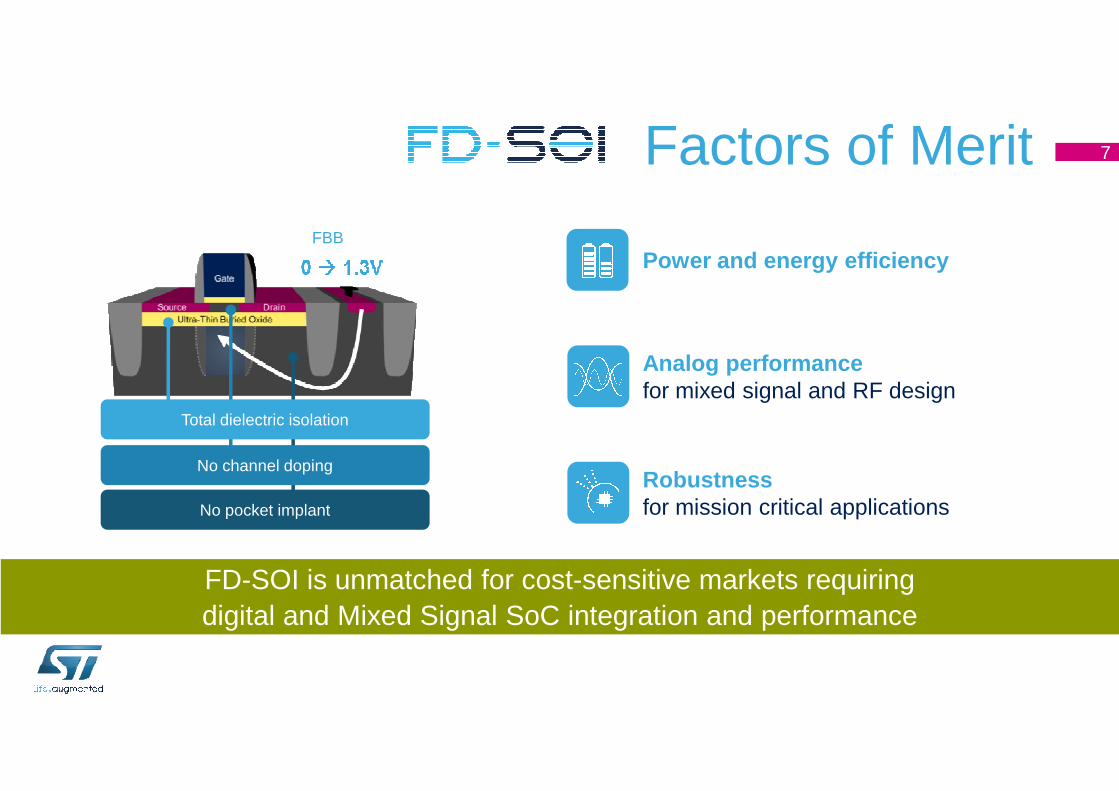
Factors of Merit 7
FBB
Power and energy efficiency
Analog performancefor mixed signal and RF design
Total dielectric isolation
No channel doping
No pocket implant
for mixed signal and RF design
Robustnessfor mission critical applications
FD-SOI is unmatched for cost-sensitive markets requiring digital and Mixed Signal SoC integration and performance
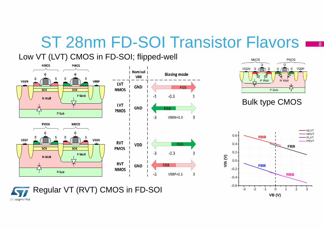
ST 28nm FD-SOI Transistor Flavors 8
Bulk type CMOS
Low VT (LVT) CMOS in FD-SOI; flipped-well
-3 -2 -1 0 1 2 3-0.6
-0.4
-0.2
0.0
0.2
0.4
0.6
FBB
RBB
RBB
FBBVth
(V
)
VB (V)
NLVT NRVT PLVT PRVT
Regular VT (RVT) CMOS in FD-SOI
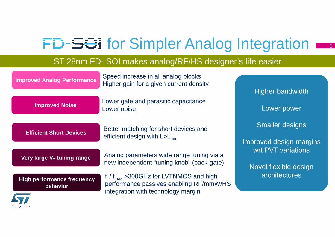
for Simpler Analog Integration 9
ST 28nm FD- SOI makes analog/RF/HS designer’s life easier
Improved Analog Performance
Improved Noise
Speed increase in all analog blocksHigher gain for a given current density
Higher bandwidth
Lower power Lower gate and parasitic capacitanceLower noise
Efficient Short DevicesSmaller designs
Improved design margins wrt PVT variations
Novel flexible design architectures
Better matching for short devices and efficient design with L>Lmin
Very large VT tuning range Analog parameters wide range tuning via a new independent “tuning knob” (back-gate)
High performance frequency behavior
fT/ fmax >300GHz for LVTNMOS and high performance passives enabling RF/mmW/HS integration with technology margin
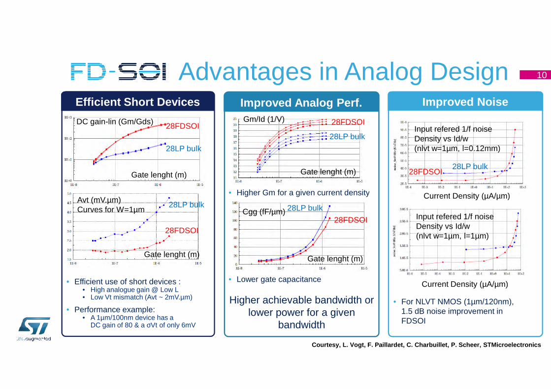
Advantages in Analog Design 10
• Higher Gm for a given current density
Efficient Short Devices Improved Analog Perf. Improved Noise
DC gain-lin (Gm/Gds)
Gate lenght (m)
28FDSOI
28LP bulk
28FDSOI
28LP bulk
Gate lenght (m)
Gm/Id (1/V)
28LP bulk28FDSOI
Input refered 1/f noiseDensity vs Id/w(nlvt w=1µm, l=0.12mm)
Current Density (µA/µm)
• Efficient use of short devices : • High analogue gain @ Low L• Low Vt mismatch (Avt ~ 2mV.µm)
• Performance example:• A 1µm/100nm device has a
DC gain of 80 & a σVt of only 6mV
• Higher Gm for a given current density
• Lower gate capacitance
Higher achievable bandwidth or lower power for a given
bandwidth
• For NLVT NMOS (1µm/120nm),1.5 dB noise improvement in FDSOI
Courtesy, L. Vogt, F. Paillardet, C. Charbuillet, P. Scheer, STMicroelectronics
Gate lenght (m)
Avt (mV.µm)Curves for W=1µm
28FDSOI
28LP bulk
Gate lenght (m)
Cgg (fF/µm) 28LP bulk
28FDSOI
Current Density (µA/µm)
Input refered 1/f noiseDensity vs Id/w(nlvt w=1µm, l=1µm)
Current Density (µA/µm)
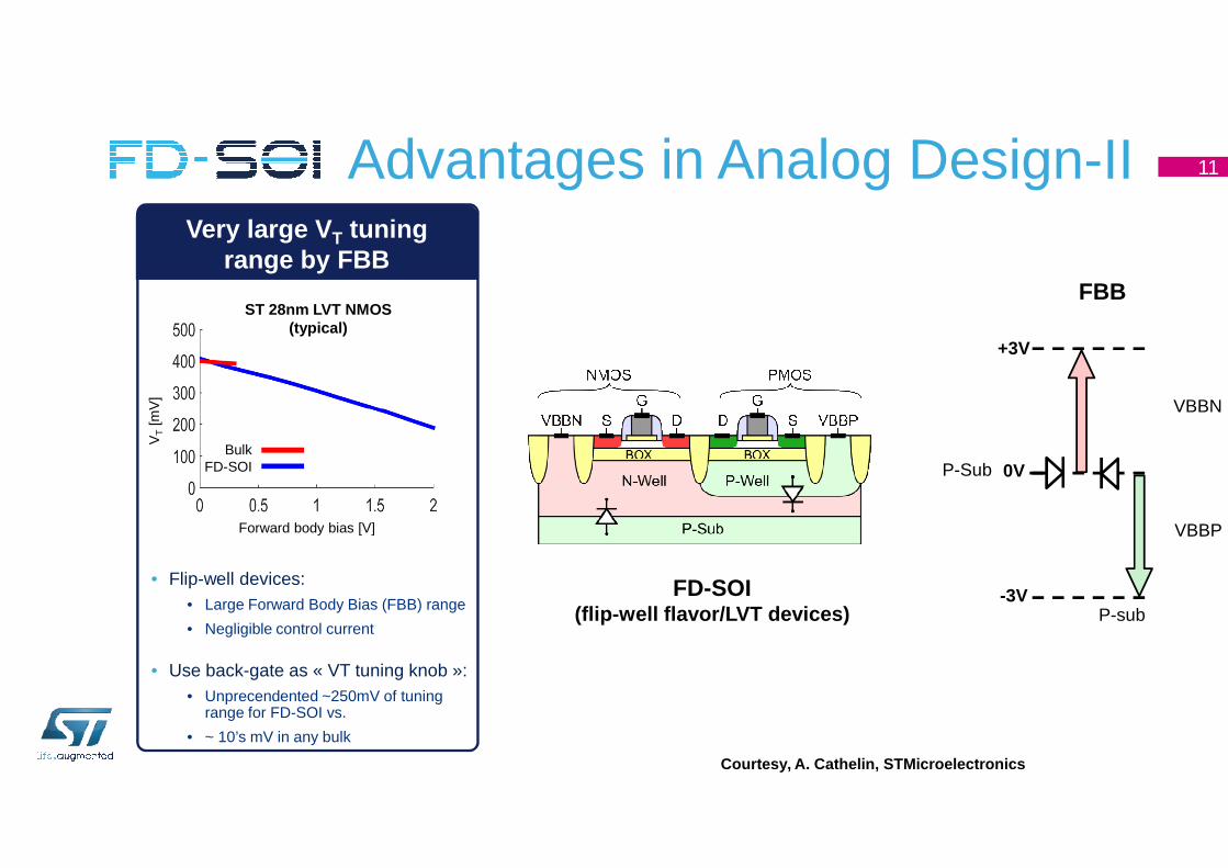
Advantages in Analog Design-II 11
Very large VT tuning range by FBB
FBB
VBBN
+3V
T[m
V]
ST 28nm LVT NMOS (typical)
• Flip-well devices:• Large Forward Body Bias (FBB) range
• Negligible control current
• Use back-gate as « VT tuning knob »: • Unprecendented ~250mV of tuning
range for FD-SOI vs.
• ~ 10’s mV in any bulk
Courtesy, A. Cathelin, STMicroelectronics
FD-SOI(flip-well flavor/LVT devices)
P-Sub
VBBP
0V
-3VP-sub
BulkFD-SOI
Forward body bias [V]
VT
Body biasing techniques for analog/MS/RF designs• Take advantage of the unique very wide-band body biasing (BB) voltage range
• Propose unique techniques bringing uncontested chip energy saving and revisiting performances SoA
•• Method 1: Method 1: BB voltage variable over time and PVT
• Cancel system level PVT effects by continously tuning transistors’ respective VT
• Design examples: J. Lechevalier ISSCC2015, D. Danilovic RFIC2016, G. De Streel VLSI2016
• Reconfigure circuit/bloc/system depending on application operation mode
12
• Reconfigure circuit/bloc/system depending on application operation mode
• Design examples: A. Larie ISSCC2015 (bloc level), G. De Streel VLSI2016 (system level)
• Propose new energy efficient design techniques for tunable blocs via body tie
• Design examples: I. Sourikopoulos ESSCIRC2016
•• Method 2:Method 2: fixed BB voltage
• Enable operation at ULV (0.5V) and in the same time increase circuit speed
• Design examples: L. Fanori RFIC2015, A. Lahiri ESSCIRC2016
• Minimize switches Ron value and excursion for energy efficient and high speed switched-capacitors circuits (e.g. ADC)
• Design examples: S. Le Tual ISSCC2014, A. Kumar ESSCIRC2016
On the usage of FBB for inverter-based Analog/RF 28nm UTBB FDSOI: example of a 450MHz Gm- C filter with IIP3> 1dBv over a 0.7-1V power supply
[J. Lechevalier at al, ISSCC2015]
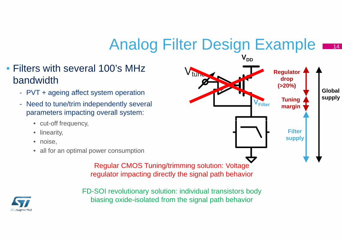
Analog Filter Design Example• Filters with several 100’s MHz
bandwidth- PVT + ageing affect system operation
- Need to tune/trim independently several parameters impacting overall system:
• cut-off frequency,
14
Global supply
VDD
VFilterTuning margin
Regulator drop
(>20%)
• cut-off frequency, • linearity, • noise, • all for an optimal power consumption
Regular CMOS Tuning/trimming solution: Voltage regulator impacting directly the signal path behavior
FD-SOI revolutionary solution: individual transistors body biasing oxide-isolated from the signal path behavior
Filter supply
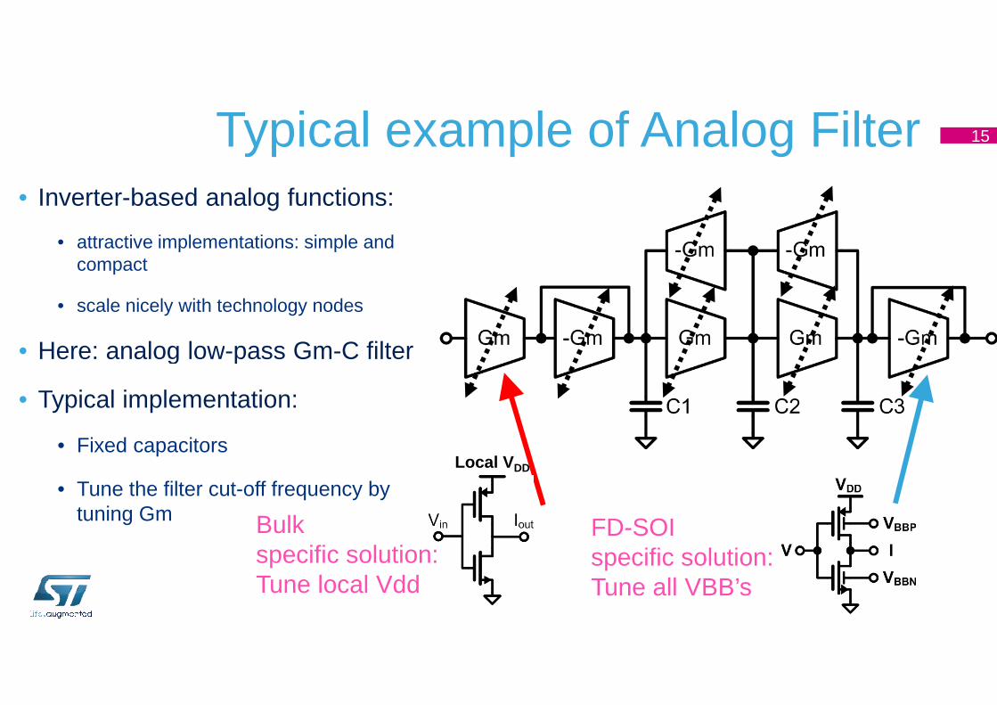
Typical example of Analog Filter• Inverter-based analog functions:
• attractive implementations: simple and compact
• scale nicely with technology nodes
• Here: analog low-pass Gm-C filter
15
• Here: analog low-pass Gm-C filter
• Typical implementation:
• Fixed capacitors
• Tune the filter cut-off frequency by tuning Gm Bulk
specific solution:Tune local Vdd
Local V DD
FD-SOIspecific solution:Tune all VBB’s
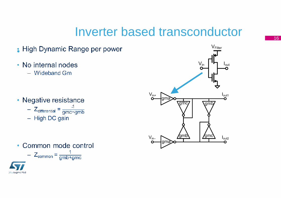
Inverter based transconductor•
16
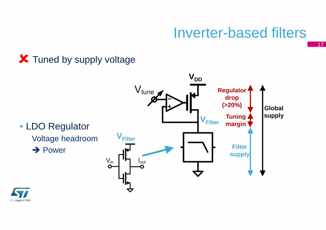
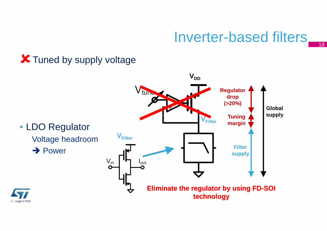
Tuned by supply voltage
Inverter-based filters
Tuning Global supply
VDD
V
Regulator drop
(>20%)
�
17
• LDO RegulatorVoltage headroom � Power
Tuning margin
Filter supply
supplyVFilter
VFilter
Global supply
VDD
V
Tuned by supply voltage
Inverter-based filters
Tuning
Regulator drop
(>20%)
�
18
Eliminate the regulator by using FDEliminate the regulator by using FD--SOI SOI technologytechnology
Filter supply
supplyVFilter
VFilter
• LDO RegulatorVoltage headroom � Power
Tuning margin
•
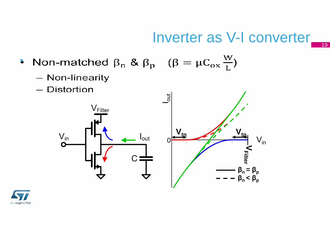
I out
Inverter as V-I converter19
βn = βpβn < βp
Vin
Vtn Vtp0 V
Filter
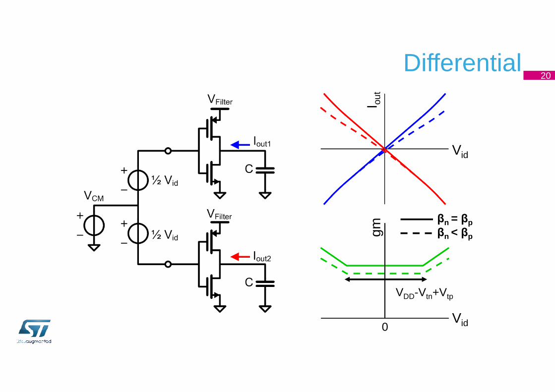
Differential
Vid
I out
20
Vid
gm
VDD-Vtn+Vtp
βn = βpβn < βp
0
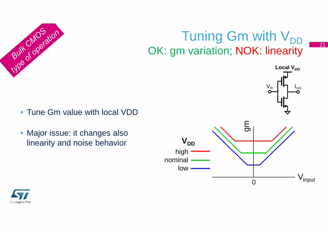
Tuning Gm with VDDOK: gm variation; NOK: linearity
21
• Tune Gm value with local VDD
Local V DD
gm
Vinput
highnominal
low
VDD
0
• Tune Gm value with local VDD
• Major issue: it changes also linearity and noise behavior

Fixed supply operation, tune by Vbody
VDD
• Eliminate LDO regulator• VFilter = VDD
22
VFilter
Vfilter = VDD
Bulk FD-SOI
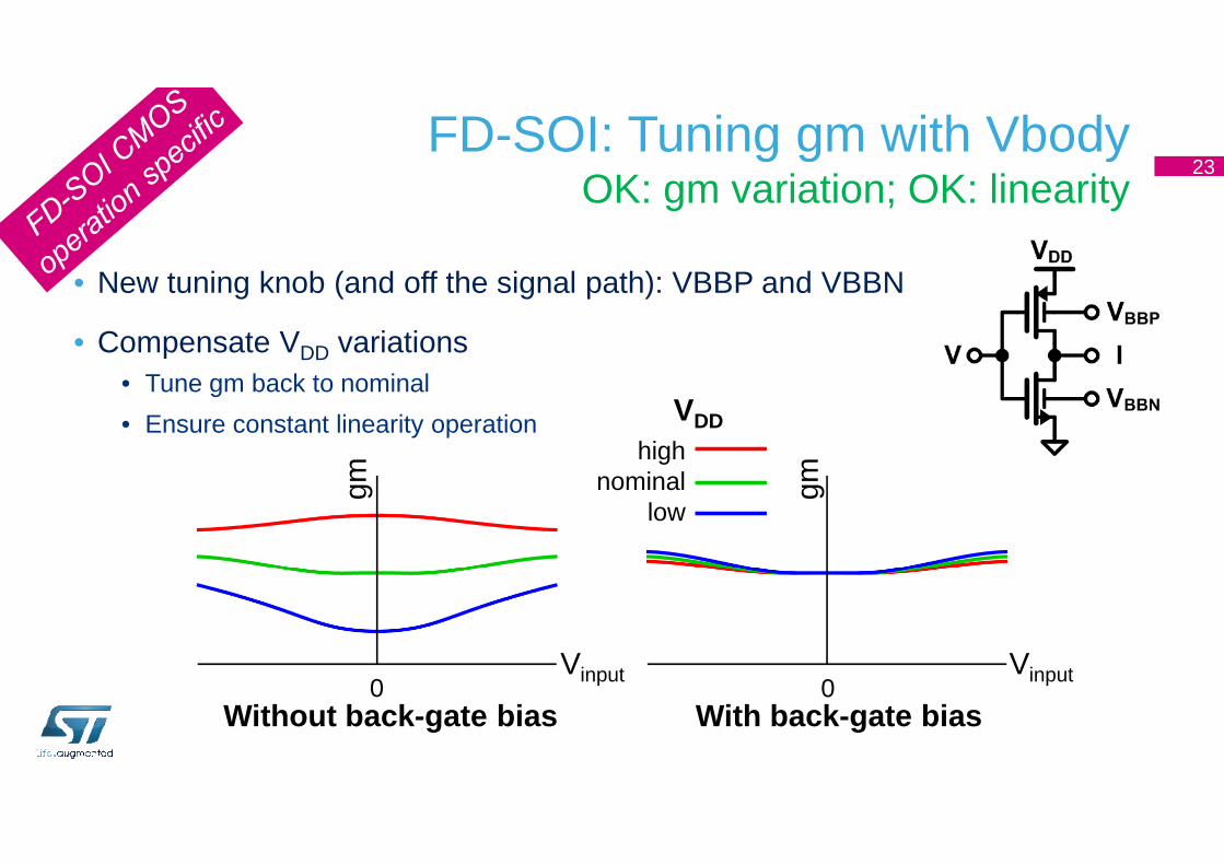
FD-SOI: Tuning gm with VbodyOK: gm variation; OK: linearity
• New tuning knob (and off the signal path): VBBP and VBBN
• Compensate VDD variations • Tune gm back to nominal
• Ensure constant linearity operation
23
VDD• Ensure constant linearity operation
Vinput
gm
Vinput
gm
Without back-gate bias With back-gate bias
highnominal
low
00
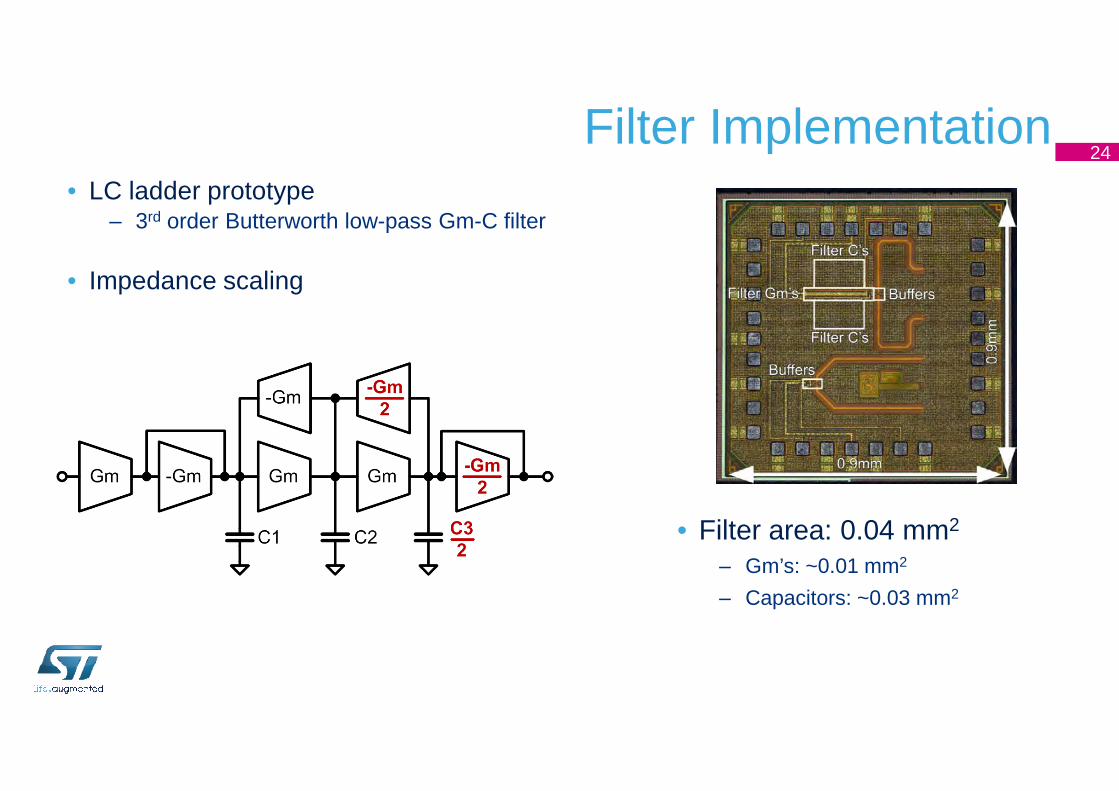
Filter Implementation• LC ladder prototype
‒ 3rd order Butterworth low-pass Gm-C filter
• Impedance scaling
24
• Filter area: 0.04 mm2
‒ Gm’s: ~0.01 mm2
‒ Capacitors: ~0.03 mm2
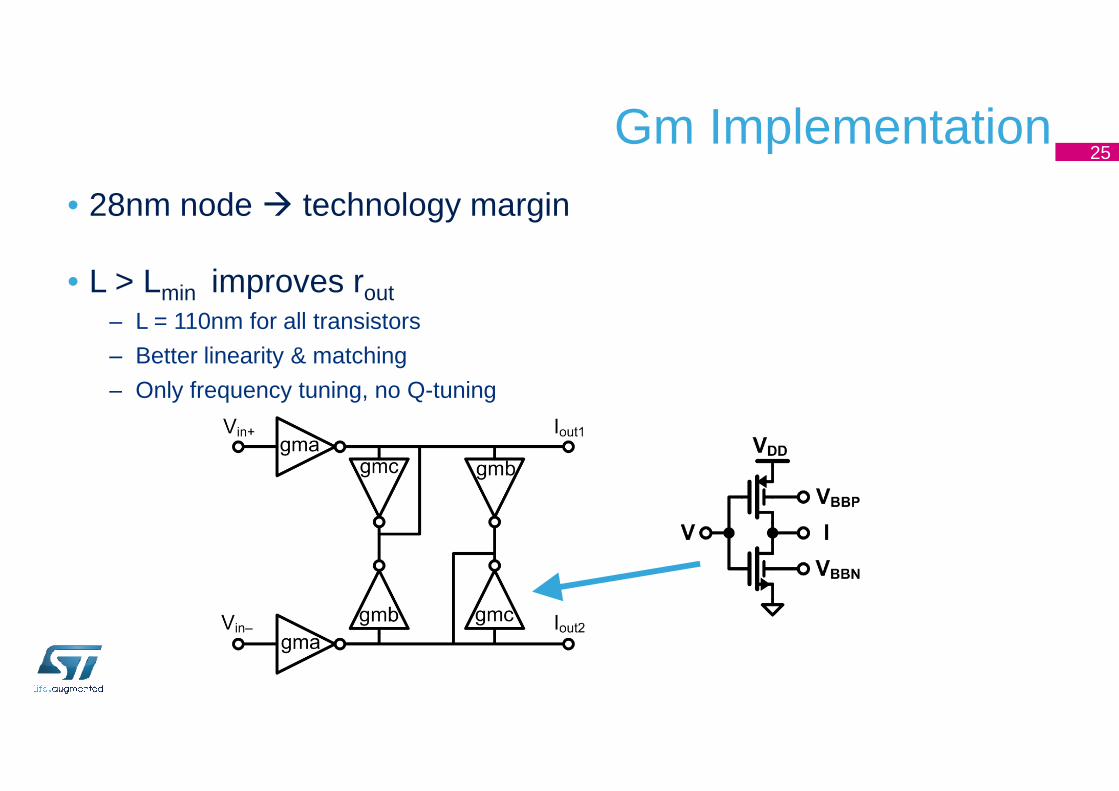
• 28nm node � technology margin
• L > Lmin improves rout‒ L = 110nm for all transistors
‒ Better linearity & matching
‒ Only frequency tuning, no Q-tuning
Gm Implementation 25
‒ Only frequency tuning, no Q-tuning
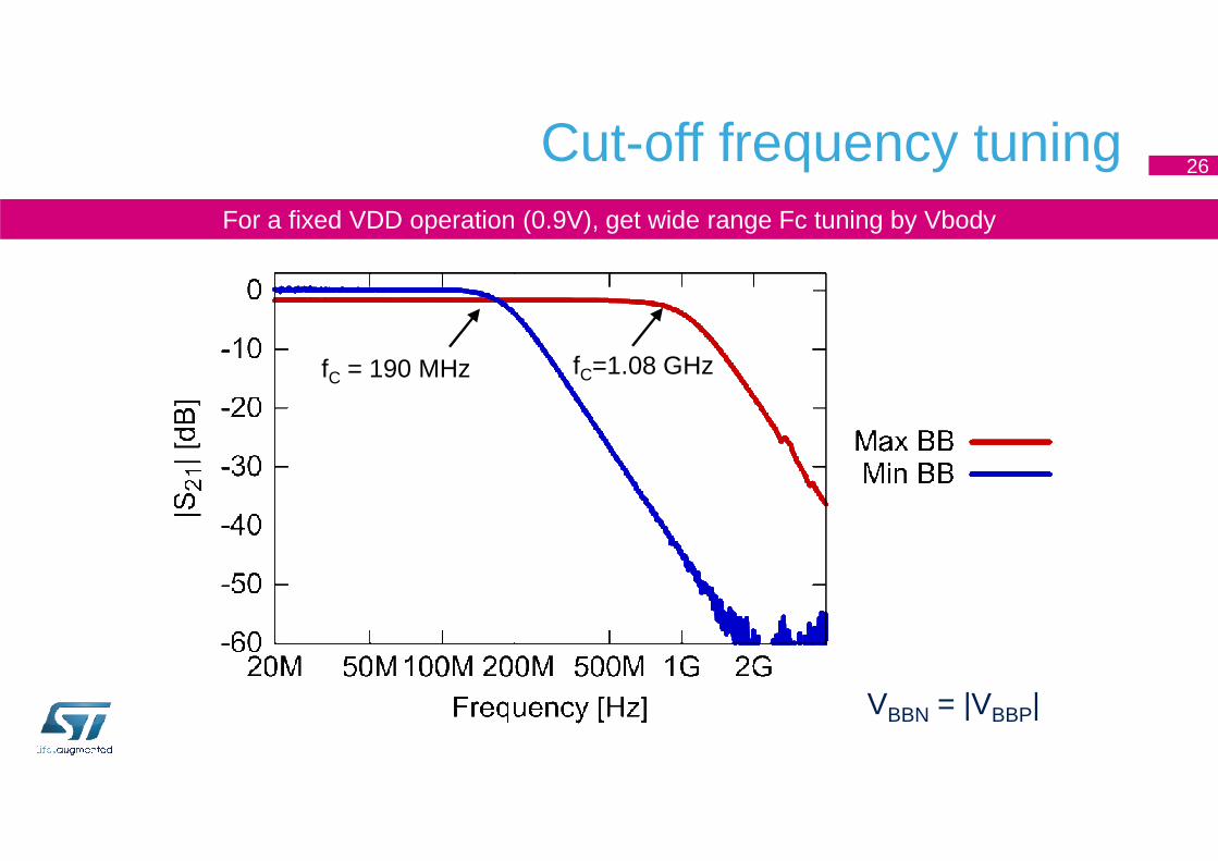
Cut-off frequency tuning
fC=1.08 GHzfC = 190 MHz
26
For a fixed VDD operation (0.9V), get wide range Fc tuning by Vbody
VBBN = |VBBP|
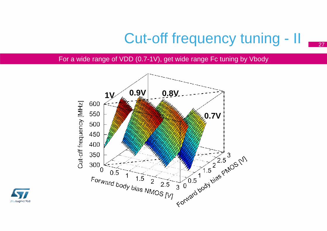
Cut-off frequency tuning - II
0.7V
0.9V1V 0.8V
27
For a wide range of VDD (0.7-1V), get wide range Fc tuning by Vbody
0.7V
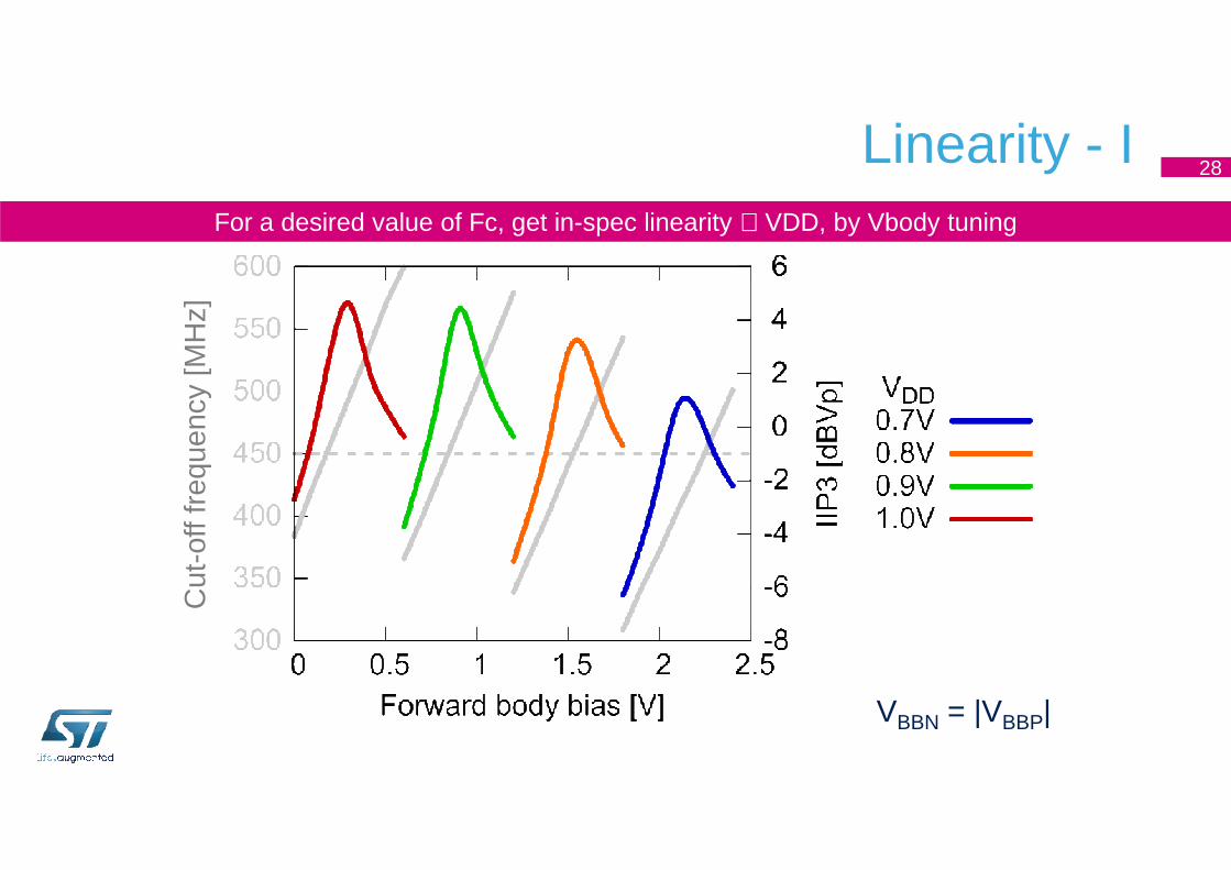
Linearity - Iof
f fre
quen
cy [M
Hz]
28
For a desired value of Fc, get in-spec linearity ∀ VDD, by Vbody tuning
VBBN = |VBBP|
Cut
-off
freq
uenc
y [M
Hz]
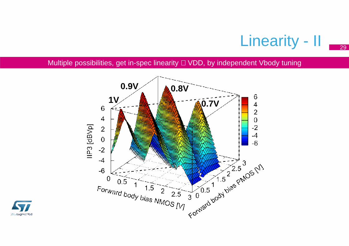
Linearity - II
0.7V
0.8V0.9V
1V
29
Multiple possibilities, get in-spec linearity ∀ VDD, by independent Vbody tuning
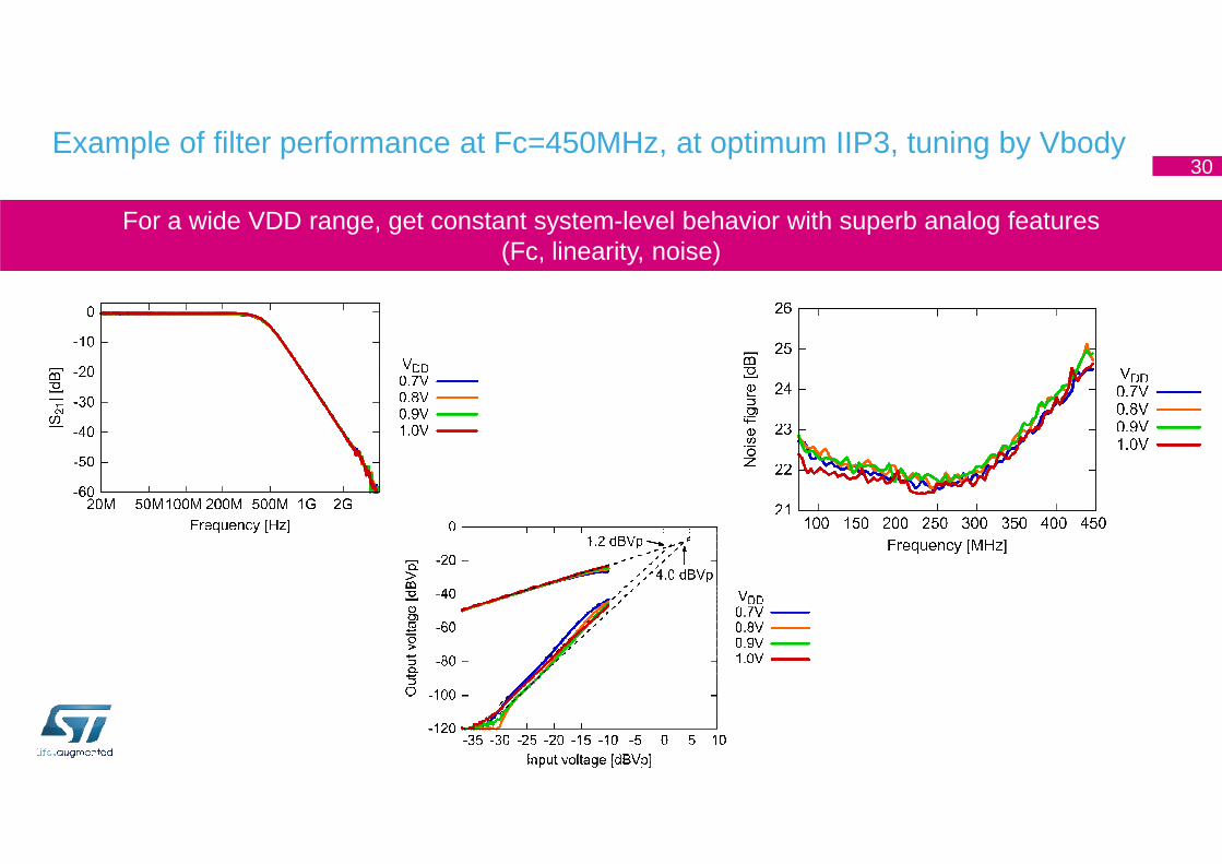
Example of filter performance at Fc=450MHz, at optimum IIP3, tuning by Vbody30
For a wide VDD range, get constant system-level behavior with superb analog features (Fc, linearity, noise)
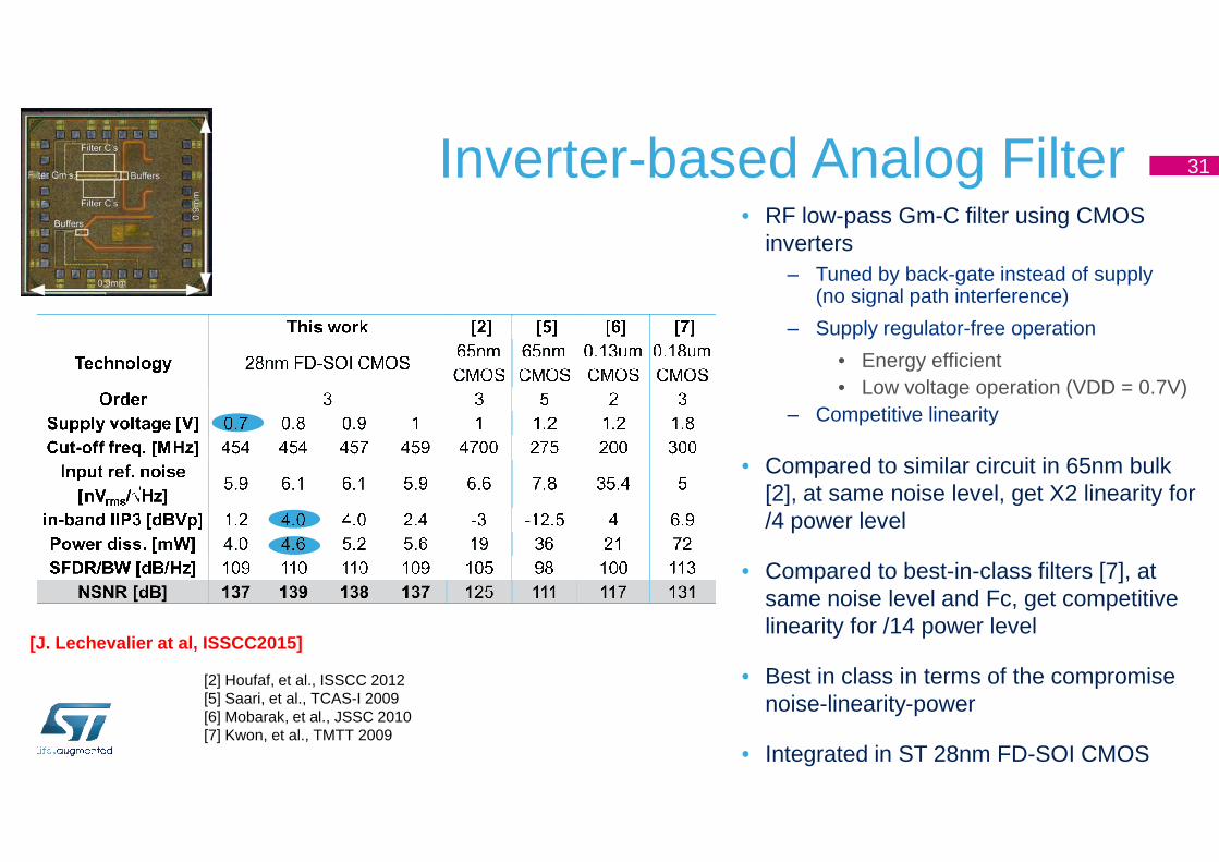
Inverter-based Analog Filter 31
• RF low-pass Gm-C filter using CMOS inverters‒ Tuned by back-gate instead of supply
(no signal path interference)
‒ Supply regulator-free operation
• Energy efficient• Low voltage operation (VDD = 0.7V)
‒ Competitive linearity
• Compared to similar circuit in 65nm bulk [2], at same noise level, get X2 linearity for /4 power level
• Compared to best-in-class filters [7], at same noise level and Fc, get competitive linearity for /14 power level
• Best in class in terms of the compromise noise-linearity-power
• Integrated in ST 28nm FD-SOI CMOS
[2] Houfaf, et al., ISSCC 2012[5] Saari, et al., TCAS-I 2009[6] Mobarak, et al., JSSC 2010[7] Kwon, et al., TMTT 2009
[J. Lechevalier at al, ISSCC2015]
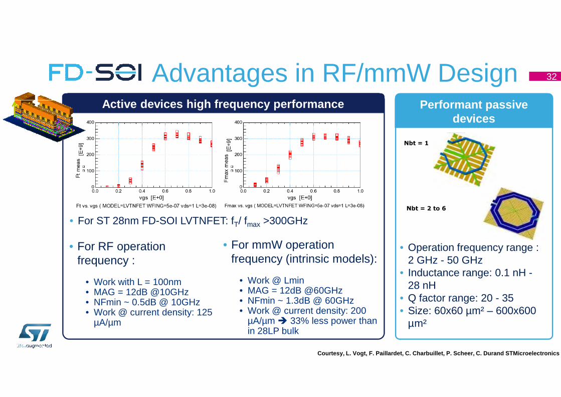
Advantages in RF/mmW Design 32
Active devices high frequency performance Performant passive devices
Nbt = 1
• For RF operationfrequency :
• Work with L = 100nm• MAG = 12dB @10GHz• NFmin ~ 0.5dB @ 10GHz• Work @ current density: 125
µA/µm
• Operation frequency range : 2 GHz - 50 GHz
• Inductance range: 0.1 nH -28 nH
• Q factor range: 20 - 35• Size: 60x60 µm² – 600x600
µm²
Courtesy, L. Vogt, F. Paillardet, C. Charbuillet, P. Scheer, C. Durand STMicroelectronics
• For mmW operationfrequency (intrinsic models):
• Work @ Lmin• MAG = 12dB @60GHz• NFmin ~ 1.3dB @ 60GHz• Work @ current density: 200
µA/µm � 33% less power thanin 28LP bulk
• For ST 28nm FD-SOI LVTNFET: fT/ fmax >300GHzNbt = 2 to 6
A 60GHz 28nm UTBB FD-SOI Reconfigurable Power Amplifier with 21% PAE, 18.2dBm P1dB and 74mW PDC
[A. Larie et al., ISSCC2015]
High dc consumption
Low average PAE
Dis
sipa
ted
pow
er [m
W]
High PAPR
60GHz PA
0
200
400
600
800
1000
1200
dc
con
sum
pti
on
[m
W]
PA
Other TX blocks
60-GHz transceivers (RF TX part)65nm
90nm
40nm
65nm65nm
WiGiG with max. operation probability @
8dB back-off � high linearity with optimized
power
34
JSSC, 2010
ISSCC, 2014
JSSC, 2013
JSSC, 2012
RFIC, 2014
ESSCIRC, 2014
RFIC, 2014
MWCL, 2015
0123456789
10
12 13 14 15 16 17 18 19 201-dB compression point [dBm]
CMOS 40nm
CMOS 65nm
PAE
at 8
-dB
bac
k-of
f [%
]
Average power
Output power [dBm]
Output powerat 8-dB back-off
50% power in mmW TRx spent in PA
Solve the general trade-off linearity and power consumption
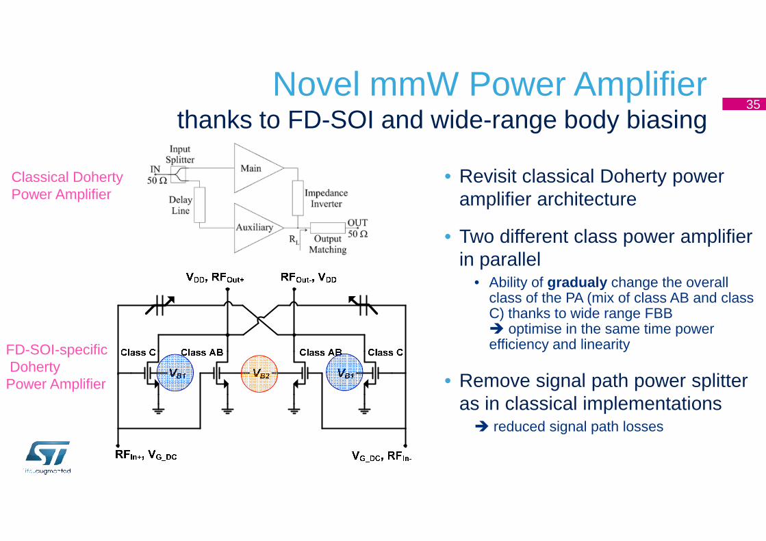
Novel mmW Power Amplifier thanks to FD-SOI and wide-range body biasing
35
• Revisit classical Doherty power amplifier architecture
• Two different class power amplifier in parallel
Classical DohertyPower Amplifier
• Ability of gradualy change the overallclass of the PA (mix of class AB and class C) thanks to wide range FBB � optimise in the same time power efficiency and linearity
• Remove signal path power splitter as in classical implementations
� reduced signal path losses
FD-SOI-specificDohertyPower Amplifier
Drain Drain
Gate Gate
Sou
rce
Sou
rce
Power transistor
Neutralization transistor
Antenna
diode
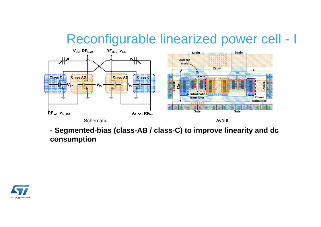
Reconfigurable linearized power cell - I
- Segmented-bias (class-AB / class-C) to improve linearity and dcconsumption
Schematic Layout
Drain Drain
Gate Gate
Sou
rce
Sou
rce
Power transistor
Neutralization transistor
Antenna
diode
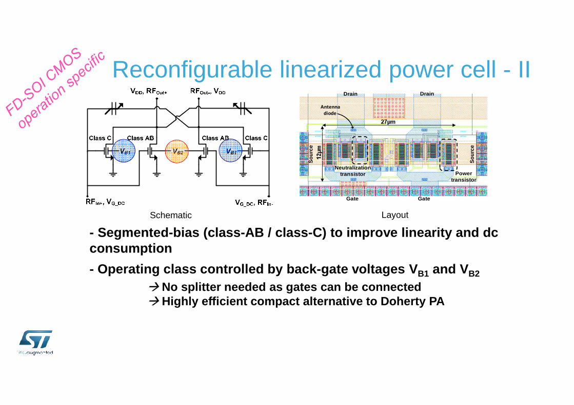
Reconfigurable linearized power cell - II
- Segmented-bias (class-AB / class-C) to improve linearity and dcconsumption
- Operating class controlled by back-gate voltages VB1 and VB2
� No splitter needed as gates can be connected� Highly efficient compact alternative to Doherty PA
Schematic Layout
Drain Drain
Gate Gate
Sou
rce
Sou
rce
Power transistor
Neutralization transistor
Antenna
diode
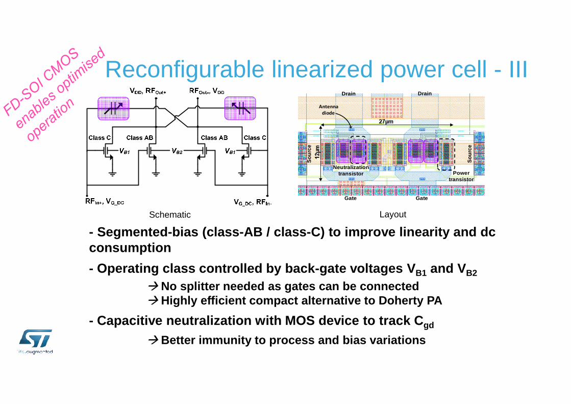
Reconfigurable linearized power cell - III
- Segmented-bias (class-AB / class-C) to improve linearity and dcconsumption
- Operating class controlled by back-gate voltages VB1 and VB2
� No splitter needed as gates can be connected� Highly efficient compact alternative to Doherty PA
- Capacitive neutralization with MOS device to track Cgd
� Better immunity to process and bias variations
Schematic Layout
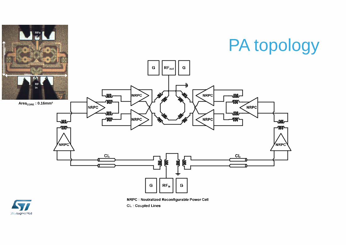
PA topology
AreaCORE : 0.16mm²
280µm
580µm
RFout
RFin
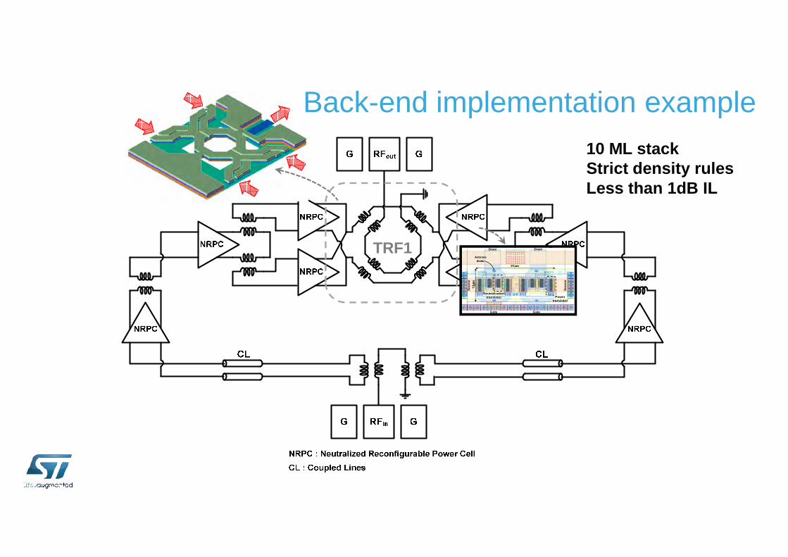
TRF1 Drain Drain
Antenna
diode
10 ML stackStrict density rulesLess than 1dB IL
Back-end implementation example
Gate Gate
Sou
rce
Sou
rce
Power transistor
Neutralization transistor
40
• S-parameters results at VDD=1.0V• Two highlighted modes : high gain & high linearity (intermediate modes possible)• > 8 GHz bandwidth • Unconditionally stable VB1 = VB2 = 2V
Small-signal measured resultsPA gain and linearity modes configured by body bias only, fixed VDD
-20
-10
0
10
20
30
40 45 50 55 60 65 70 75 80
S21
[dB
]
Freq [GHz]
High linearity mode
High gain mode
VB1 = 0V, VB2 = 0.8V
B1 B2
20
25
30
35
40
20
25
30
35
40
PA
E [
%]
Ga
in [
dB
]
20
25
30
35
40
20
25
30
35
40
PA
E [
%]
Ga
in [
dB
]
High gain mode
High linearity mode
Continuous tuning
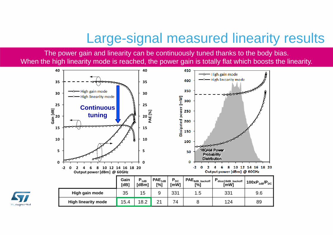
Large-signal measured linearity resultsThe power gain and linearity can be continuously tuned thanks to the body bias.
When the high linearity mode is reached, the power gain is totally flat which boosts the linearity.
0
5
10
15
20
0
5
10
15
20
-2 0 2 4 6 8 10 12 14 16 18 20
PA
E [
%]
Ga
in [
dB
]
Output power [dBm] @ 60GHz
0
5
10
15
20
0
5
10
15
20
-2 0 2 4 6 8 10 12 14 16 18 20
PA
E [
%]
Ga
in [
dB
]
Output power [dBm] @ 60GHz
Gain [dB]
P1dB[dBm]
PAE1dB[%]
PDC[mW]
PAE8dB_backoff[%]
Pdiss@8dB_backoff[mW]
100xP1dB/PDC
High gain mode 35 15 9 331 1.5 331 9.6
High linearity mode 15.4 18.2 21 74 8 124 89
tuning
This work S. Kulkarni ISSCC 2014
D. Zhao JSSC 2013
D. Zhao JSSC 2012
E. Kaymaksut RFIC 2014
A. Siligaris JSSC 2010
Technology 28nm UTBB FD-SOI 40nm 40nm 40nm 40nm 65nm PD-SOI
Operating mode High g ain High l inearity NA Low/High power NA NA NA
Supply voltage [V] 1.0 1.0 0.8 0.9 1.0 1.0 0.9 1.8
Freq. [GHz] 61 60 60 63 61 60 77 60
Gain [dB] 35 15.4 15.1 22.4 16.8 / 17 26 9 16
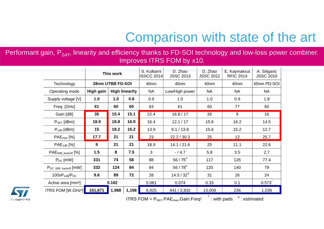
Performant gain, PSAT, linearity and efficiency thanks to FD-SOI technology and low-loss power combiner.Improves ITRS FOM by x10.
Comparison with state of the art
Gain [dB] 35 15.4 15.1 22.4 16.8 / 17 26 9 16
PSAT [dBm] 18.9 18.8 16.9 16.4 12.1 / 17 15.6 16.2 14.5
P1dB [dBm] 15 18.2 16.2 13.9 9.1 / 13.8 15.6 15.2 12.7
PAEmax [%] 17.7 21 21 23 22.2 / 30.3 25 12 25.7
PAE1dB [%] 9 21 21 18.9 14.1 / 21.6 25 11.1 22.6
PAE8dB_backoff [%] 1.5 8 7.5 3 - / 4.7 5.8 3.5 2.7
PDC [mW] 331 74 58 88 56 / 75# 117 126 77.4
PDC_8dB_backoff [mW] 332 124 84 94 56 / 78# 120 140 79
100xP1dB/PDC 9.6 89 72 28 14.5 / 32# 31 26 24
Active area [mm²] 0.162 0.081 0.074 0.33 0.1 0.573*
ITRS FOM [W.GHz²] 161,671 1,988 1,198 6,925 641 / 2,832 13,009 236 1,038
ITRS FOM = PSAT.PAEmax.Gain.Freq² * : with pads # : estimated
This work S. Kulkarni ISSCC 2014
D. Zhao JSSC 2013
D. Zhao JSSC 2012
E. Kaymaksut RFIC 2014
A. Siligaris JSSC 2010
Technology 28nm UTBB FD-SOI 40nm 40nm 40nm 40nm 65nm PD-SOI
Operating mode High g ain High l inearity NA Low/High power NA NA NA
Supply voltage [V] 1.0 1.0 0.8 0.9 1.0 1.0 0.9 1.8
Freq. [GHz] 61 60 60 63 61 60 77 60
Gain [dB] 35 15.4 15.1 22.4 16.8 / 17 26 9 16
The high linearity mode reduces the dissipated energy at 8dB back-off with no compromise in linearity.
Comparison with state of the art
PSAT [dBm] 18.9 18.8 16.9 16.4 12.1 / 17 15.6 16.2 14.5
P1dB [dBm] 15 18.2 16.2 13.9 9.1 / 13.8 15.6 15.2 12.7
PAEmax [%] 17.7 21 21 23 22.2 / 30.3 25 12 25.7
PAE1dB [%] 9 21 21 18.9 14.1 / 21.6 25 11.1 22.6
PAE8dB_backoff [%] 1.5 8 7.5 3 - / 4.7 5.8 3.5 2.7
PDC [mW] 331 74 58 88 56 / 75# 117 126 77.4
PDC_8dB_backoff [mW] 332 124 84 94 56 / 78# 120 140 79
100xP1dB/PDC 9.6 89 72 28 14.5 / 32# 31 26 24
Active area [mm²] 0.162 0.081 0.074 0.33 0.1 0.573*
ITRS FOM [W.GHz²] 161,671 1,988 1,198 6,925 641 / 2,832 13,009 236 1,038
ITRS FOM = PSAT.PAEmax.Gain.Freq² * : with pads # : estimated
This work S. Kulkarni ISSCC 2014
D. Zhao JSSC 2013
D. Zhao JSSC 2012
E. Kaymaksut RFIC 2014
A. Siligaris JSSC 2010
Technology 28nm UTBB FD-SOI 40nm 40nm 40nm 40nm 65nm PD-SOI
Operating mode High g ain High l inearity NA Low/High power NA NA NA
Supply voltage [V] 1.0 1.0 0.8 0.9 1.0 1.0 0.9 1.8
Freq. [GHz] 61 60 60 63 61 60 77 60
Gain [dB] 35 15.4 15.1 22.4 16.8 / 17 26 9 16
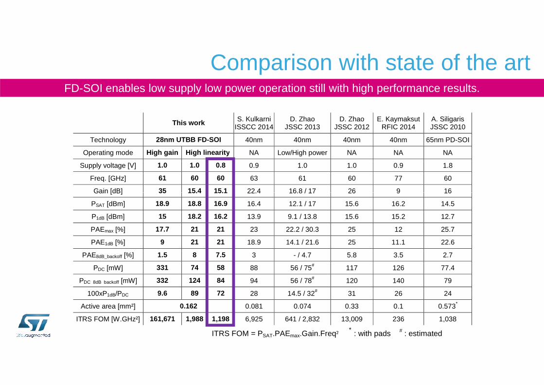
FD-SOI enables low supply low power operation still with high performance results.
Comparison with state of the art
Gain [dB] 35 15.4 15.1 22.4 16.8 / 17 26 9 16
PSAT [dBm] 18.9 18.8 16.9 16.4 12.1 / 17 15.6 16.2 14.5
P1dB [dBm] 15 18.2 16.2 13.9 9.1 / 13.8 15.6 15.2 12.7
PAEmax [%] 17.7 21 21 23 22.2 / 30.3 25 12 25.7
PAE1dB [%] 9 21 21 18.9 14.1 / 21.6 25 11.1 22.6
PAE8dB_backoff [%] 1.5 8 7.5 3 - / 4.7 5.8 3.5 2.7
PDC [mW] 331 74 58 88 56 / 75# 117 126 77.4
PDC_8dB_backoff [mW] 332 124 84 94 56 / 78# 120 140 79
100xP1dB/PDC 9.6 89 72 28 14.5 / 32# 31 26 24
Active area [mm²] 0.162 0.081 0.074 0.33 0.1 0.573*
ITRS FOM [W.GHz²] 161,671 1,988 1,198 6,925 641 / 2,832 13,009 236 1,038
ITRS FOM = PSAT.PAEmax.Gain.Freq² * : with pads # : estimated
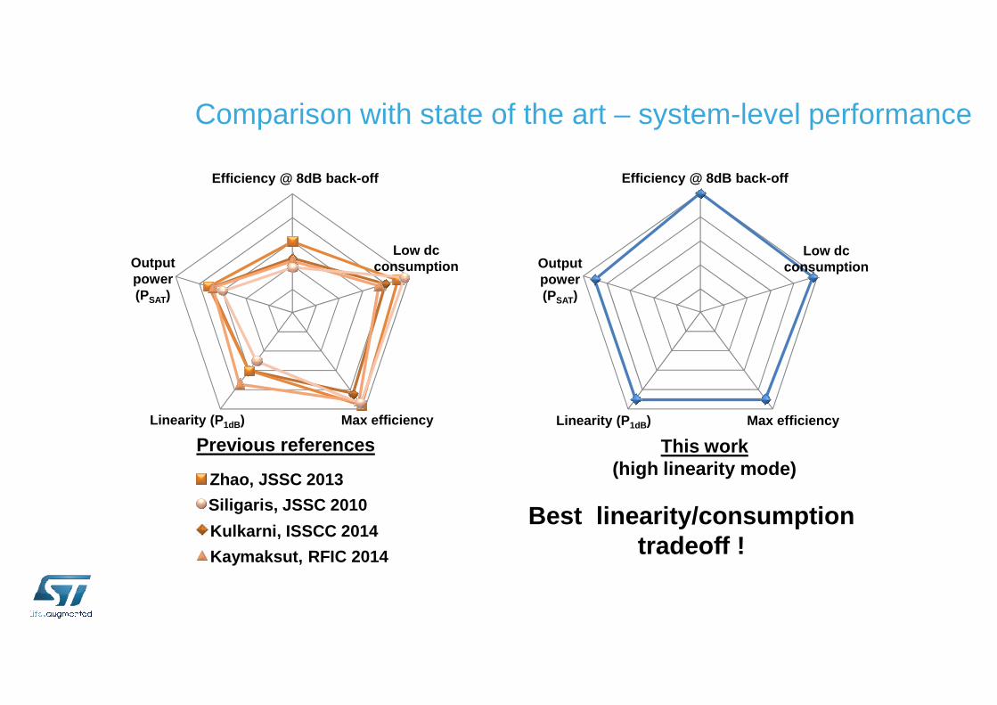
Efficiency @ 8dB back-off
Low dc consumptionOutput
power (PSAT)
Efficiency @ 8dB back-off
Low dc consumptionOutput
power (PSAT)
Comparison with state of the art – system-level performance
Max efficiencyLinearity (P 1dB) Max efficiencyLinearity (P 1dB)
Zhao, JSSC 2013
Siligaris, JSSC 2010
Kulkarni, ISSCC 2014
Kaymaksut, RFIC 2014
This work (high linearity mode)
Previous references
Best linearity/consumption tradeoff !
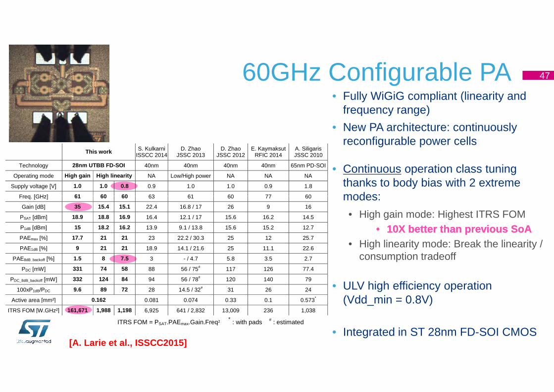
60GHz Configurable PA 47
• Fully WiGiG compliant (linearity and frequency range)
• New PA architecture: continuously reconfigurable power cells
• Continuous operation class tuning thanks to body bias with 2 extreme modes:
This work S. Kulkarni ISSCC 2014
D. Zhao JSSC 2013
D. Zhao JSSC 2012
E. Kaymaksut RFIC 2014
A. Siligaris JSSC 2010
Technology 28nm UTBB FD-SOI 40nm 40nm 40nm 40nm 65nm PD-SOI
Operating mode High gain High linearity NA Low/High power NA NA NA
Supply voltage [V] 1.0 1.0 0.8 0.9 1.0 1.0 0.9 1.8
Freq. [GHz] 61 60 60 63 61 60 77 60 modes:
• High gain mode: Highest ITRS FOM•• 10X better than previous 10X better than previous SoASoA
• High linearity mode: Break the linearity / consumption tradeoff
• ULV high efficiency operation (Vdd_min = 0.8V)
• Integrated in ST 28nm FD-SOI CMOS
Freq. [GHz] 61 60 60 63 61 60 77 60
Gain [dB] 35 15.4 15.1 22.4 16.8 / 17 26 9 16
PSAT [dBm] 18.9 18.8 16.9 16.4 12.1 / 17 15.6 16.2 14.5
P1dB [dBm] 15 18.2 16.2 13.9 9.1 / 13.8 15.6 15.2 12.7
PAEmax [%] 17.7 21 21 23 22.2 / 30.3 25 12 25.7
PAE1dB [%] 9 21 21 18.9 14.1 / 21.6 25 11.1 22.6
PAE8dB_backoff [%] 1.5 8 7.5 3 - / 4.7 5.8 3.5 2.7
PDC [mW] 331 74 58 88 56 / 75# 117 126 77.4
PDC_8dB_backoff [mW] 332 124 84 94 56 / 78# 120 140 79
100xP1dB/PDC 9.6 89 72 28 14.5 / 32# 31 26 24
Active area [mm²] 0.162 0.081 0.074 0.33 0.1 0.573*
ITRS FOM [W.GHz²] 161,671 1,988 1,198 6,925 641 / 2,832 13,009 236 1,038
ITRS FOM = PSAT.PAEmax.Gain.Freq² * : with pads # : estimated
[A. Larie et al., ISSCC2015]
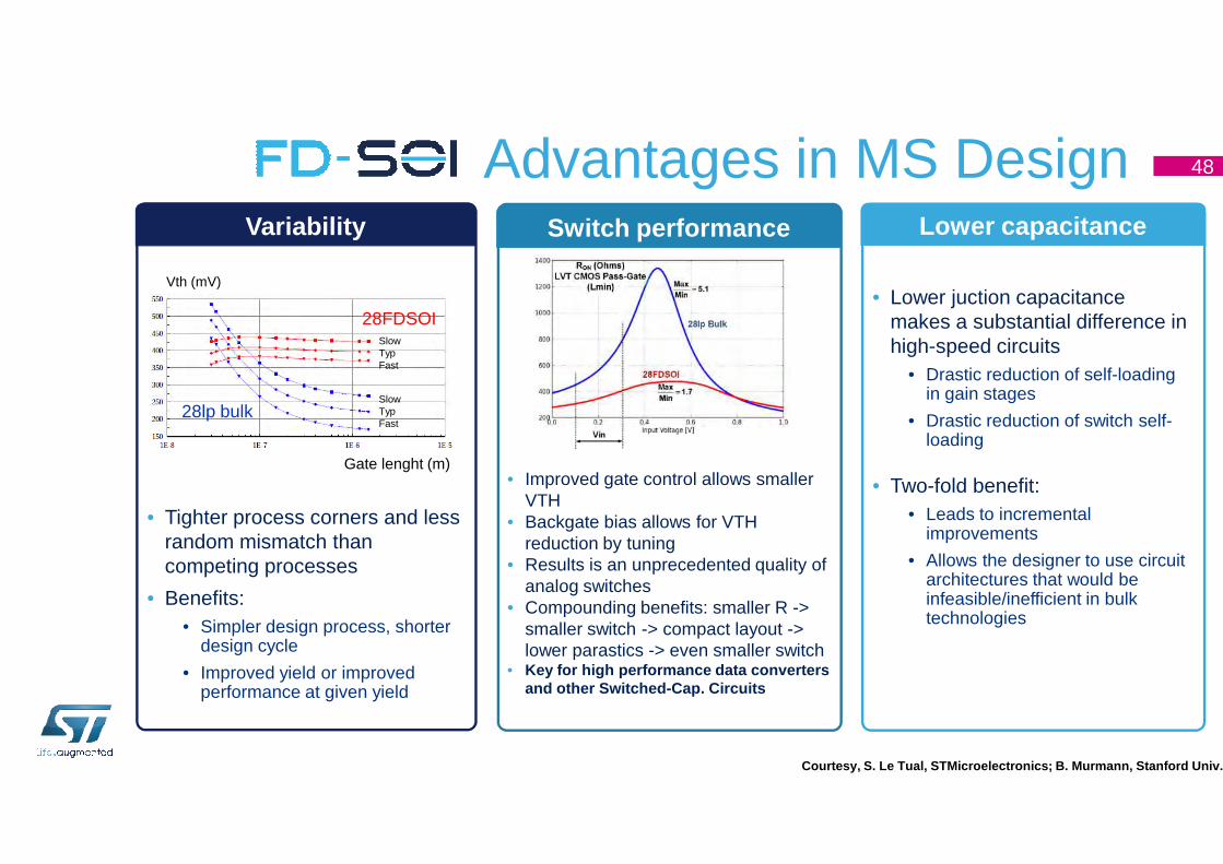
Advantages in MS Design 48
Variability Switch performance Lower capacitance
• Lower juction capacitance makes a substantial difference in high-speed circuits
• Drastic reduction of self-loading in gain stages
• Drastic reduction of switch self-loading
Vth (mV)
28FDSOI
28lp bulk
SlowTypFast
SlowTypFast
• Tighter process corners and less random mismatch than competing processes
• Benefits:• Simpler design process, shorter
design cycle
• Improved yield or improved performance at given yield
Courtesy, S. Le Tual, STMicroelectronics; B. Murmann, Stanford Univ.
• Improved gate control allows smaller VTH
• Backgate bias allows for VTH reduction by tuning
• Results is an unprecedented quality of analog switches
• Compounding benefits: smaller R -> smaller switch -> compact layout -> lower parastics -> even smaller switch
• Key for high performance data converters and other Switched-Cap. Circuits
loading
• Two-fold benefit:• Leads to incremental
improvements
• Allows the designer to use circuit architectures that would be infeasible/inefficient in bulk technologies
Gate lenght (m)
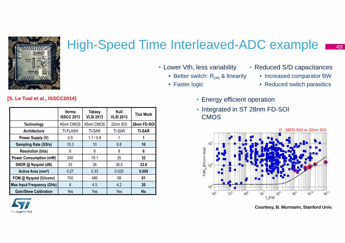
High-Speed Time Interleaved-ADC example 49
• Lower Vth, less variability• Better switch: RON & linearity
• Faster logic
• Reduced S/D capacitances• Increased comparator BW
• Reduced switch parasitics
Verma
ISSCC 2013
Tabasy
VLSI 2013
Kull
VLSI 2013This Work
[S. Le Tual et al., ISSCC2014] • Energy efficient operation
• Integrated in ST 28nm FD-SOI CMOS
Technology 40nm CMOS 65nm CMOS 32nm SOI 28nm FD-SOI
Architecture TI-FLASH TI-SAR TI-SAR TI-SAR
Power Supply (V) 0.9 1.1 / 0.9 1 1
Sampling Rate (GS/s) 10.3 10 8.8 10
Resolution (bits) 6 6 8 6
Power Consumption (mW) 240 79.1 35 32
SNDR @ Nyquist (dB) 33 26 38.5 33.8
Active Area (mm2) 0.27 0.33 0.025 0.009
FOM @ Nyquist (fJ/conv) 700 480 58 81
Max Input Frequency (GHz) 6 4.5 4.2 20
Gain/Skew Calibration Yes Yes Yes No
O : 28FD-SOI or 32nm SOI
Courtesy, B. Murmann, Stanford Univ.
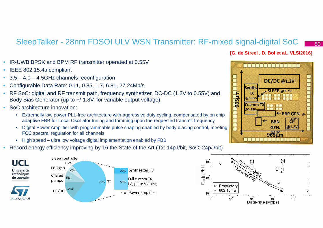
SleepTalker - 28nm FDSOI ULV WSN Transmitter: RF-mixed signal-digital SoC
• IR-UWB BPSK and BPM RF transmitter operated at 0.55V• IEEE 802.15.4a compliant
• 3.5 – 4.0 – 4.5GHz channels reconfiguration• Configurable Data Rate: 0.11, 0.85, 1.7, 6.81, 27.24Mb/s
• RF SoC: digital and RF transmit path, frequency synthetizer, DC-DC (1.2V to 0.55V) and Body Bias Generator (up to +/-1.8V, for variable output voltage)
• SoC architecture innovation:• Extremelly low power PLL-free architecture with aggressive duty cycling, compensated by on chip
50
[G. de Streel , D. Bol et al., VLSI2016]
• Extremelly low power PLL-free architecture with aggressive duty cycling, compensated by on chip adaptive FBB for Local Oscillator tuning and trimming upon the requested transmit frequency
• Digital Power Amplifier with programmable pulse shaping enabled by body biasing control, meeting FCC spectral regulation for all channels
• High speed – ultra low voltage digital implementation enabled by FBB
• Record energy efficiency improving by 16 the State of the Art (Tx: 14pJ/bit, SoC: 24pJ/bit)
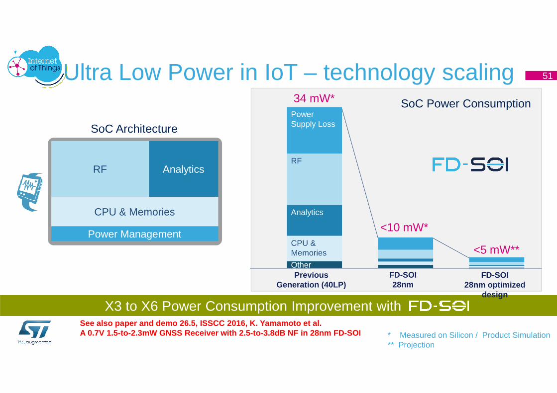
RF Analytics
Ultra Low Power in IoT – technology scaling 51
Power Supply Loss
RF
SoC Architecture
SoC Power Consumption34 mW*
CPU & Memories
Power Management
Analytics
CPU & Memories
Other
<10 mW*
<5 mW**
X3 to X6 Power Consumption Improvement with FD-SOI
PreviousGeneration (40LP)
FD-SOI28nm
FD-SOI28nm optimized
design
* Measured on Silicon / Product Simulation ** Projection
See also paper and demo 26.5, ISSCC 2016, K. Yamamoto et al. A 0.7V 1.5-to-2.3mW GNSS Receiver with 2.5-to-3.8dB NF in 28nm FD-SOI
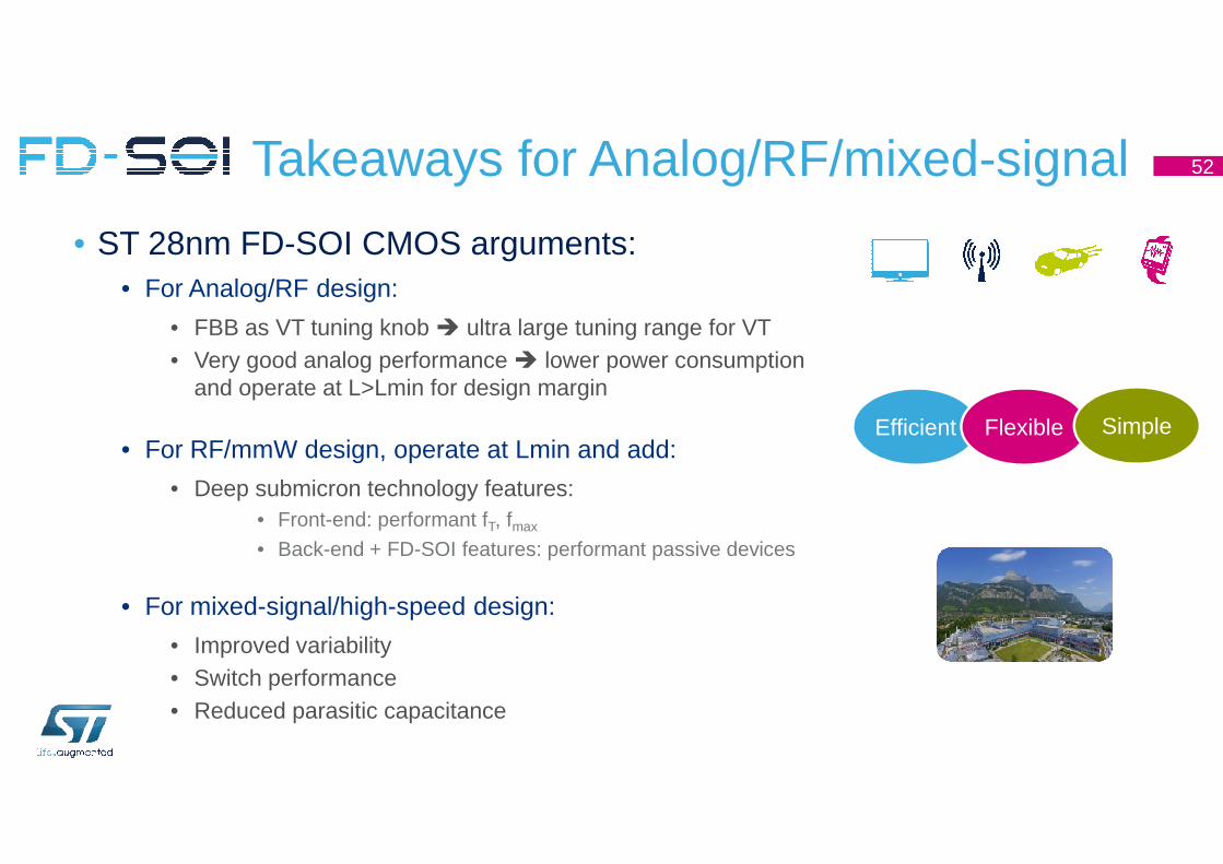
Takeaways for Analog/RF/mixed-signal
• ST 28nm FD-SOI CMOS arguments:• For Analog/RF design:
• FBB as VT tuning knob � ultra large tuning range for VT• Very good analog performance � lower power consumption
and operate at L>Lmin for design margin
52
Efficient Flexible Simple• For RF/mmW design, operate at Lmin and add:
• Deep submicron technology features:• Front-end: performant fT, fmax
• Back-end + FD-SOI features: performant passive devices
• For mixed-signal/high-speed design:
• Improved variability• Switch performance• Reduced parasitic capacitance
Efficient Flexible Simple

Take-aways charts per field
Analog/RF design in FD-SOI• FD-SOI arguments:
• FBB as VT tuning knob � ultra large tuning range for VT
• Very good analog performance � lower power consumption and operate at L>Lmin for design margin
• Consequences on analog/RF design:
54
• Consequences on analog/RF design:• Operate amplifiers at constant Gm
• Employ new tuning strategies
• Competitive noise and linearity behavior
• Obtain strong design independence with respect to PVT variations
• New robust design oportunities
RF/mmW design in FD-SOI• FD-SOI arguments:
• FBB as VT tuning knob � ultra large tuning range for VT
• Very good analog performance � lower power consumption
• Deep submicron technology:
• Front-end: performant fT, fmax
• Back-end + FD-SOI features: performant passive devices
55
• Back-end + FD-SOI features: performant passive devices
• Consequences on RF/mmW design:• New family of reconfigurable topologies; new design architectures
• Power efficient solutions
• State of the art implementations with concomitent optimisation for each system-level parameter
• New robust design oportunities
Mixed-signal / High-speed design in FD-SOI
• FD-SOI arguments:• Improved variability
• Switch performance
• Reduced parasitic capacitance
• Consequences on MS design:
56
• Consequences on MS design:• State of the art HS Data Converters
• Drastic improvement of the Nyquist FOM (FOM=P/(fs*2ENOB) )
• New robust design oportunities and new design architectures enabled

Thank You