24-VAC Power Stage With Wide VIN Converter and … Power Stage With Wide VIN Converter and Battery...
39
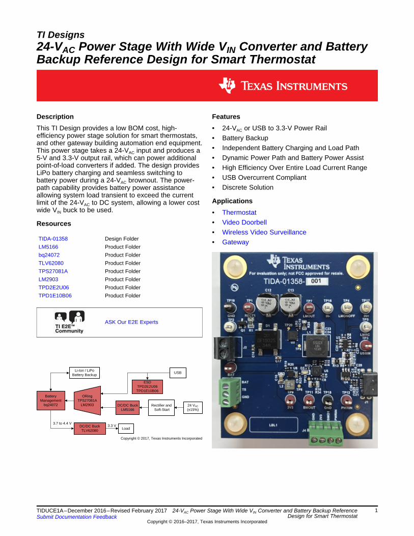
Battery Management bq24072 Li-Ion / LiPo Battery Backup ESD TPD2E2U06 TPD1E10B06 DC/DC Buck TLV62080 DC/DC Buck LM5166 USB Rectifier and Soft-Start 24 VAC (±15%) Load ORing TPS27081A LM2903 3.3 V 3.7 to 4.4 V Copyright © 2017, Texas Instruments Incorporated 1 TIDUCE1A – December 2016 – Revised February 2017 Submit Documentation Feedback Copyright © 2016–2017, Texas Instruments Incorporated 24-V AC Power Stage With Wide V IN Converter and Battery Backup Reference Design for Smart Thermostat TI Designs 24-V AC Power Stage With Wide V IN Converter and Battery Backup Reference Design for Smart Thermostat Description This TI Design provides a low BOM cost, high- efficiency power stage solution for smart thermostats, and other gateway building automation end equipment. This power stage takes a 24-V AC input and produces a 5-V and 3.3-V output rail, which can power additional point-of-load converters if added. The design provides LiPo battery charging and seamless switching to battery power during a 24-V AC brownout. The power- path capability provides battery power assistance allowing system load transient to exceed the current limit of the 24-V AC to DC system, allowing a lower cost wide V IN buck to be used. Resources TIDA-01358 Design Folder LM5166 Product Folder bq24072 Product Folder TLV62080 Product Folder TPS27081A Product Folder LM2903 Product Folder TPD2E2U06 Product Folder TPD1E10B06 Product Folder ASK Our E2E Experts Features • 24-V AC or USB to 3.3-V Power Rail • Battery Backup • Independent Battery Charging and Load Path • Dynamic Power Path and Battery Power Assist • High Efficiency Over Entire Load Current Range • USB Overcurrent Compliant • Discrete Solution Applications • Thermostat • Video Doorbell • Wireless Video Surveillance • Gateway
Transcript of 24-VAC Power Stage With Wide VIN Converter and … Power Stage With Wide VIN Converter and Battery...
Battery Management
bq24072
Li-Ion / LiPoBattery Backup
ESDTPD2E2U06TPD1E10B06
DC/DC BuckTLV62080
DC/DC BuckLM5166
USB
Rectifier and Soft-Start
24 VAC (±15%)
Load
ORingTPS27081A
LM2903
3.3 V3.7 to 4.4 V
Copyright © 2017, Texas Instruments Incorporated
1TIDUCE1A–December 2016–Revised February 2017Submit Documentation Feedback
Copyright © 2016–2017, Texas Instruments Incorporated
24-VAC Power Stage With Wide VIN Converter and Battery Backup ReferenceDesign for Smart Thermostat
TI Designs24-VAC Power Stage With Wide VIN Converter and BatteryBackup Reference Design for Smart Thermostat
DescriptionThis TI Design provides a low BOM cost, high-efficiency power stage solution for smart thermostats,and other gateway building automation end equipment.This power stage takes a 24-VAC input and produces a5-V and 3.3-V output rail, which can power additionalpoint-of-load converters if added. The design providesLiPo battery charging and seamless switching tobattery power during a 24-VAC brownout. The power-path capability provides battery power assistanceallowing system load transient to exceed the currentlimit of the 24-VAC to DC system, allowing a lower costwide VIN buck to be used.
Resources
TIDA-01358 Design FolderLM5166 Product Folderbq24072 Product FolderTLV62080 Product FolderTPS27081A Product FolderLM2903 Product FolderTPD2E2U06 Product FolderTPD1E10B06 Product Folder
ASK Our E2E Experts
Features• 24-VAC or USB to 3.3-V Power Rail• Battery Backup• Independent Battery Charging and Load Path• Dynamic Power Path and Battery Power Assist• High Efficiency Over Entire Load Current Range• USB Overcurrent Compliant• Discrete Solution
Applications• Thermostat• Video Doorbell• Wireless Video Surveillance• Gateway
System Overview www.ti.com
2 TIDUCE1A–December 2016–Revised February 2017Submit Documentation Feedback
Copyright © 2016–2017, Texas Instruments Incorporated
24-VAC Power Stage With Wide VIN Converter and Battery Backup ReferenceDesign for Smart Thermostat
An IMPORTANT NOTICE at the end of this TI reference design addresses authorized use, intellectual property matters and otherimportant disclaimers and information.
1 System Overview
1.1 System DescriptionA typical home uses a 24-VAC system to power the HVAC system. Thermostats, as well as many otherhome automation equipment, use this 24-VAC for power. Therefore, a power stage is needed to rectify the24-VAC and supply a DC voltage at the levels required by the thermostats internal components. Low cost istypically a priority for thermostat designs as board space is often plentiful enough to avoid small-footprint,high-cost parts. For thermostats implementing a chargeable battery backup system, high efficiency alsobecomes a priority to allow a smaller, and therefore lower cost, battery to be used. The TIDA-01358focuses on these priorities and can be easily adjusted to meet specific needs.
In addition to the 24-VAC and battery backup, this TI Design allows a USB power supply to be used forcharging and powering the system. Having two supply options, 24 VAC and USB, requires an ORingdevice. ORing and power mux devices can be high in cost and therefore are avoided by designers; this TIDesign provides a discrete based ORing solution that cuts costs significantly over fully featured integratedsolutions. If a USB is not desired, device can be removed with very minimal changes to the design.
The 24 VAC is rectified and stepped down to a 5-V rail using an ultra-low IQ, wide VIN, 500-mA buckconverter. The wide VIN of the buck converter helps handle transients, thus eliminating the need for a TVSdiode and other protection circuitry. Smaller capacitors may be used as the input voltage ripple can behigher when using a wide VIN buck.
The TIDA-01358 uses a battery management device that allows independent current paths and monitoringfor system power and battery charging. This device increases the cycle life of the battery. This TI Designfeatures a seamless transition to battery power should the main supply fail, as well as battery power assistshould the load requirement surpass the main supply's rating. A very efficient, low cost, and low BOMcount buck converter is used to step down the battery management voltage to 3.3 V for use by the generalsystem. Both DC-DC buck converters in this design feature low-load power saving feature to provide highefficiency even at light loads.
1.2 Key System Specifications
Table 1. Key System Specifications
PARAMETER SPECIFICATIONS NOTESTarget application Thermostat, gateway building automation —Main Input power source 20 VAC —Secondary input power source USB —LM5166 (RectOut to LMOut) efficiency 87.0% 160-mA outputTLV62080 (Battery to 3.3 V) efficiency 96.6% 160-mA output
LM5166 load regulation 1.41% 160-mA nominal output current and24-VAC nominal input voltage
TLV62080 load regulation 0.12% 160-mA nominal output current andnominal 3.7-V battery input
LM5166 max output current 500 mA 5-V busTLV62080 max output current 1 A 3.3-V busWorking environment Indoor —Form factor 52.324×64.262-mm rectangular PCB —
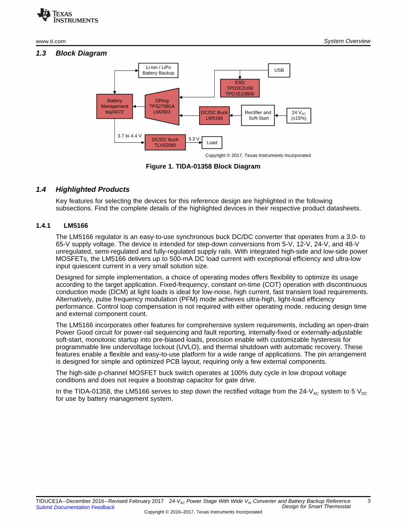
Battery Management
bq24072
Li-Ion / LiPoBattery Backup
ESDTPD2E2U06TPD1E10B06
DC/DC BuckTLV62080
DC/DC BuckLM5166
USB
Rectifier and Soft-Start
24 VAC (±15%)
Load
ORingTPS27081A
LM2903
3.3 V3.7 to 4.4 V
Copyright © 2017, Texas Instruments Incorporated
www.ti.com System Overview
3TIDUCE1A–December 2016–Revised February 2017Submit Documentation Feedback
Copyright © 2016–2017, Texas Instruments Incorporated
24-VAC Power Stage With Wide VIN Converter and Battery Backup ReferenceDesign for Smart Thermostat
1.3 Block Diagram
Figure 1. TIDA-01358 Block Diagram
1.4 Highlighted ProductsKey features for selecting the devices for this reference design are highlighted in the followingsubsections. Find the complete details of the highlighted devices in their respective product datasheets.
1.4.1 LM5166The LM5166 regulator is an easy-to-use synchronous buck DC/DC converter that operates from a 3.0- to65-V supply voltage. The device is intended for step-down conversions from 5-V, 12-V, 24-V, and 48-Vunregulated, semi-regulated and fully-regulated supply rails. With integrated high-side and low-side powerMOSFETs, the LM5166 delivers up to 500-mA DC load current with exceptional efficiency and ultra-lowinput quiescent current in a very small solution size.
Designed for simple implementation, a choice of operating modes offers flexibility to optimize its usageaccording to the target application. Fixed-frequency, constant on-time (COT) operation with discontinuousconduction mode (DCM) at light loads is ideal for low-noise, high current, fast transient load requirements.Alternatively, pulse frequency modulation (PFM) mode achieves ultra-high, light-load efficiencyperformance. Control loop compensation is not required with either operating mode, reducing design timeand external component count.
The LM5166 incorporates other features for comprehensive system requirements, including an open-drainPower Good circuit for power-rail sequencing and fault reporting, internally-fixed or externally-adjustablesoft-start, monotonic startup into pre-biased loads, precision enable with customizable hysteresis forprogrammable line undervoltage lockout (UVLO), and thermal shutdown with automatic recovery. Thesefeatures enable a flexible and easy-to-use platform for a wide range of applications. The pin arrangementis designed for simple and optimized PCB layout, requiring only a few external components.
The high-side p-channel MOSFET buck switch operates at 100% duty cycle in low dropout voltageconditions and does not require a bootstrap capacitor for gate drive.
In the TIDA-01358, the LM5166 serves to step down the rectified voltage from the 24-VAC system to 5 VDCfor use by battery management system.
4
6
5
2
3
1
Copyright © 2017, Texas Instruments Incorporated
System Overview www.ti.com
4 TIDUCE1A–December 2016–Revised February 2017Submit Documentation Feedback
Copyright © 2016–2017, Texas Instruments Incorporated
24-VAC Power Stage With Wide VIN Converter and Battery Backup ReferenceDesign for Smart Thermostat
1.4.2 bq24072The bq2407x series of devices are integrated Li-Ion sources linear chargers and system power pathmanagement devices targeted at space-limited portable applications. The devices operate from either aUSB port or an AC adapter and support charge currents up to 1.5 A. The input voltage range with inputovervoltage protection supports unregulated adapters. The USB input current limit accuracy and start upsequence allow the bq2407x to meet USB-IF inrush current specifications. Additionally, the input dynamicpower management (VIN-DPM) prevents the charger from crashing incorrectly configured USB wall adapterssources.
The bq2407x features dynamic power path management (DPPM) that powers the system whilesimultaneously and independently charging the battery. The DPPM circuit reduces the charge currentwhen the input current limit causes the system output to fall to the DPPM threshold; thus, supplying thesystem load at all times while monitoring the charge current separately. This feature reduces the numberof charge and discharge cycles on the battery, allows for proper charge termination and enables thesystem to run with a defective or absent battery pack.
1.4.3 TLV62080The TLV6208x device focuses on high-efficiency step-down conversion over a wide output current range.At medium to heavy loads, the TLV6208x converter operates in PWM mode and automatically enterspower save mode operation at light-load currents to maintain high efficiency over the entire load currentrange.
The TLV62080 synchronous switched-mode converters are based on DCS-Control™. DCS-Control is anadvanced regulation topology that combines the advantages of hysteresis and voltage mode control.
Features:• 2.5- to 5.5-V input voltage range• 100% duty cycle for lowest dropout• Power good output• Power save mode for light load efficiency• DCS-Control architecture for fast transient regulation
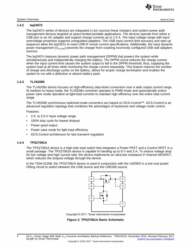
1.4.4 TPS27081AThe TPS27081A device is a high-side load switch that integrates a Power PFET and a Control NFET in asmall package. The TPS27081A device is capable fo handing up to 8 V and 3 A. To reduce voltage dropfor low voltage and high current rails, the device implements an ultra-low resistance P-channel MOSFET,which reduces the dropout voltage through the device.
In the TIDA-01358, the TPS27081A device is used in conjunction with the LM2903 in a low-cost powerORing circuit to switch between the USB source and the LM5166 source.
Figure 2. TPS27081A Basic Schematic
www.ti.com System Overview
5TIDUCE1A–December 2016–Revised February 2017Submit Documentation Feedback
Copyright © 2016–2017, Texas Instruments Incorporated
24-VAC Power Stage With Wide VIN Converter and Battery Backup ReferenceDesign for Smart Thermostat
1.4.5 LM2903The LM2903 consists of two independent voltage comparators that are designed to operate from a singlepower supply over a wide range of voltages. This standard device has proven ubiquity and versatilityacross a wide range of applications. This is due to very wide supply voltages range (2 to 36 V), low IQ andfast response of the devices.
The open-drain output allows the user to configure the output's logic low voltage (VOL) and can be usedto enable the comparator to be used in AND functionality.
Features:• Low output saturation voltage• Maximum rating: 2 to 36 V• Low input bias current: 25 nA (typical)• Common-mode input voltage range includes ground
The LM2903 is used as the logic for the power ORing circuit in the TIDA-01358.
1.4.6 TPD2E2U06The TPD2E2U06 is a dual-channel low capacitance TVS diode electrostatic discharge (ESD) protectiondevice. The device offers ±25-kV contact and ±30-kV air-gap ESD protection in accordance with the IEC61000-4-2 standard. The 1.5-pF line capacitance of the TPD2E2U06 makes the device suitable for a widerange of applications. Typical application interfaces are USB 2.0, LVDS, and I2C.
Features:• 5.5-A peak pulse current (8/29-µs pulse)• Ultra-low leakage current 10 nA (max)• Low ESD clamping voltage• DC breakdown voltage 6.5 V (min)
The TPD2E2U06 is used on the USB communicated lines in the TIDA-01358.
1.4.7 TPD1E10B06The TPD1E10B06 device is a single-channel 1 ESD transient voltage suppression (TVS) diode in a small0402 package. This TVS protection product offers ±30-kV contact ESD, ±30-kV IEC air-gap protection,and has an ESD clamp circuit with a back-to-back TVS diode for bipolar or bidirectional signal support.The 12-pF line capacitance of this ESD protection diode is suitable for a wide range of applicationssupporting data rates up to 400 Mbps. The 0402 package is an industry standard and is convenient forcomponent placement in space-saving applications.
Typical applications of this ESD protection product are circuit protection for audio lines (microphone,earphone, and speakerphone), SD interfacing, keypad or other buttons, VBUS pin and ID pin of USBports, and general-purpose I/O ports. This ESD clamp is good for the protection of the end equipment likeebooks, tablets, remote controllers, wearables, set-top boxes, and electronic point of sale equipment.
The TPD1E10B06 is used to protect the USB VBUS pin on the TIDA-01358.
2
2 3
R 150 k42 V 42 V 10.4 V
R R 150 k 453 k
æ ö æ öç ÷ ç ÷
è øè ø
W= =
+ W + W
System Design Theory www.ti.com
6 TIDUCE1A–December 2016–Revised February 2017Submit Documentation Feedback
Copyright © 2016–2017, Texas Instruments Incorporated
24-VAC Power Stage With Wide VIN Converter and Battery Backup ReferenceDesign for Smart Thermostat
2 System Design TheoryThe TIDA-01358 provides the main power stages needed for building automation electronics that areprimarily powered from the 24-VAC system used in typical homes. This TI Design presents a systemsolution that is modular in design, allowing system designers to easily modify the design if necessary tomore closely match their product's specifications.
Cost reduction is a priority in this TI Design. Efficiency, particularly when using the battery backup, andheat loss are taken into consideration as well. To keep costs low, avoiding an over engineered system isrequired. The discrete nature of the TIDA-01358 allows designers to easily remove features they do notneed, or easily add features and power rails that are required for their specific application.
This section outlines the theory and design considerations used to develop and design the TIDA-01358.
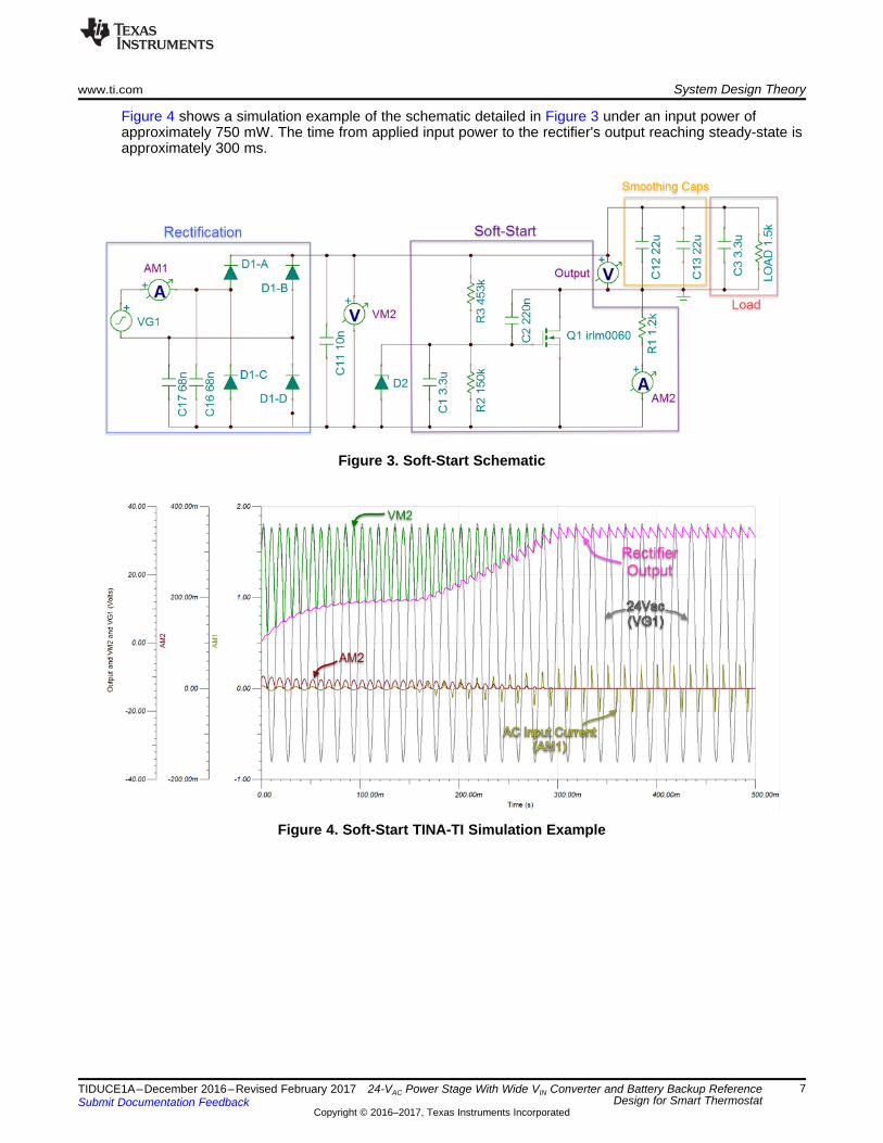
2.1 24-VAC to DC RectificationA full-bridge rectifier is used for DC rectification. To prevent a significantly large inrush current during initialconnection of 24 VAC, a soft-start circuit is implemented.
The schematic shown in Figure 3 shows the rectification and soft-start process. C1, C2, and C3 functionas high frequency bypass capacitors. R1, R2, C4, and C5 provide the soft-start time constant for the gateof the N-channel MOSFET (T1). Q1 has a gate threshold voltage range of 1.0 to 2.5 V and a 92-mΩRDS(on)max at VGS = 10 V. The values of R2 and R3 are chosen to voltage divide a maximum of 42 V (thepeak of the 24 VAC at the high end of its tolerance) down to approximately 10 V once steady state hasbeen reached. Calculating R2 and R3 is shown in Equation 1:
(1)
Z1 is used as a protective device for the MOSFET gate. R4 is used to provide an initial current path whileT1 is still open. The use of R4 prevents significantly differing soft-start times due to variances in the 24-VAC transformer and Q1's gate threshold voltage. The resulting circuit provides a relatively consistent soft-start time regardless of the 24-VAC source variances.
C6 and C7 function as the rectifier's smoothing capacitors. The TIDA-01358 has a maximum power outputof 3.3 W. The output ripple will be a function of the load current. TINA-TI™ simulation shows a maximumworst case ripple of 11.7 V. This maximum assumes 4.3 W is required at the input to produce 3.3 W at theoutput and occurs when the 24-VAC transformer is at the low-voltage edge of its tolerance and the outputpower of the 3.3-V rail is outputting its maximum current of 1 A. That worst case condition is typicallyunlikely to occur depending on application; a more reasonable use case of a 100-mA output from the 3.3-V rail and a nominal 24-VAC transformer provides a rectification ripple of approximately 1.4 V. These ripplevoltages must be checked in each application it is used. Even at the worse case scenario as previouslyoutlined, the LM5166 buck converter is capable of handling those ripple voltages and voltage ranges.
www.ti.com System Design Theory
7TIDUCE1A–December 2016–Revised February 2017Submit Documentation Feedback
Copyright © 2016–2017, Texas Instruments Incorporated
24-VAC Power Stage With Wide VIN Converter and Battery Backup ReferenceDesign for Smart Thermostat
Figure 4 shows a simulation example of the schematic detailed in Figure 3 under an input power ofapproximately 750 mW. The time from applied input power to the rectifier's output reaching steady-state isapproximately 300 ms.
Figure 3. Soft-Start Schematic
Figure 4. Soft-Start TINA-TI Simulation Example
( )18 18 18sw 22 23
5 5C C C 480 pF
f R R 309 k 100 k138 kH
||z
309 k 100 k
³ Þ ³ Þ ³´ W ´ W
´W + W
æ öç ÷è ø
22 23
OUT
1.223 V 1.223 VR R 100 k 333 k
V 1.223 V 5 1.223 V= ´ = ´ W = W
- -
( )( )
( )
4 4OUT
5 RT
sw
V V 10 5.0 V 10R R k 226 k
f kHz 1.75 130 kHz 1.75= W = = ´ =´ W
GND GND
LMOut
GND
100k
R4LMOut
RectOut
GND
SW1
VIN2
ILIM3
SS4
RT5
PGOOD6
EN7
VOUT/FB8
HYS9
GND10
PAD11
U2
LM5166DRCR226kR5
475k
R21
GND
100pFC20
3300pF
C18
0.033µFC19
3.3µFC3
22µFC24
GND GND
TP7
TP19
TP6
TP20GND
0
R32
100µH
L1
LMSW
100kR23
309kR22
47µFC23
Copyright © 2016, Texas Instruments Incorporated
System Design Theory www.ti.com
8 TIDUCE1A–December 2016–Revised February 2017Submit Documentation Feedback
Copyright © 2016–2017, Texas Instruments Incorporated
24-VAC Power Stage With Wide VIN Converter and Battery Backup ReferenceDesign for Smart Thermostat
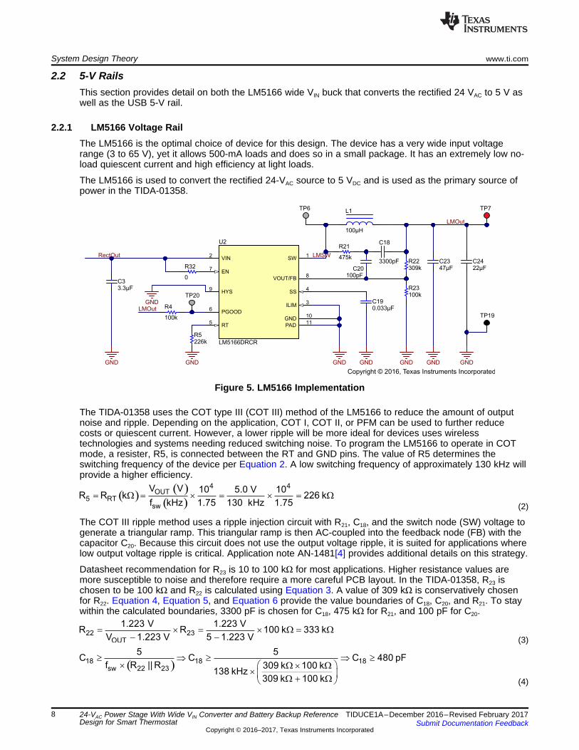
2.2 5-V RailsThis section provides detail on both the LM5166 wide VIN buck that converts the rectified 24 VAC to 5 V aswell as the USB 5-V rail.
2.2.1 LM5166 Voltage RailThe LM5166 is the optimal choice of device for this design. The device has a very wide input voltagerange (3 to 65 V), yet it allows 500-mA loads and does so in a small package. It has an extremely low no-load quiescent current and high efficiency at light loads.
The LM5166 is used to convert the rectified 24-VAC source to 5 VDC and is used as the primary source ofpower in the TIDA-01358.
Figure 5. LM5166 Implementation
The TIDA-01358 uses the COT type III (COT III) method of the LM5166 to reduce the amount of outputnoise and ripple. Depending on the application, COT I, COT II, or PFM can be used to further reducecosts or quiescent current. However, a lower ripple will be more ideal for devices uses wirelesstechnologies and systems needing reduced switching noise. To program the LM5166 to operate in COTmode, a resister, R5, is connected between the RT and GND pins. The value of R5 determines theswitching frequency of the device per Equation 2. A low switching frequency of approximately 130 kHz willprovide a higher efficiency.
(2)
The COT III ripple method uses a ripple injection circuit with R21, C18, and the switch node (SW) voltage togenerate a triangular ramp. This triangular ramp is then AC-coupled into the feedback node (FB) with thecapacitor C20. Because this circuit does not use the output voltage ripple, it is suited for applications wherelow output voltage ripple is critical. Application note AN-1481[4] provides additional details on this strategy.
Datasheet recommendation for R23 is 10 to 100 kΩ for most applications. Higher resistance values aremore susceptible to noise and therefore require a more careful PCB layout. In the TIDA-01358, R23 ischosen to be 100 kΩ and R22 is calculated using Equation 3. A value of 309 kΩ is conservatively chosenfor R22. Equation 4, Equation 5, and Equation 6 provide the value boundaries of C18, C20, and R21. To staywithin the calculated boundaries, 3300 pF is chosen for C18, 475 kΩ for R21, and 100 pF for C20.
(3)
(4)
( )L nom
Out 23 24 23 24 23 24
SW LMOut
I 311mAC C C C C C C 14 F
8 f V 8 138 kHz 20mV
D= + ³ Þ + ³ Þ + ³ m
´ ´ D ´ ´
( ) ( )( )L nom
L1 peak OUT max
I 311mAI I 500 mA 656 mA
2 2
D= + = + =
( )LMOut LMOut
L nom
SW IN
V V 5 V 5 VI 1 1 311mA
f L1 V 138 kHz 100 H 35 V
æ ö æ öD = ´ - = ´ - =ç ÷ ç ÷´ ´ m è øè ø
( )
LMOut LMOut
SW OutL nom
V V 5 V 5 VL1 1 1 124 H
f I Rect 138 kHz 250 mA 35 V
æ ö æ ö= ´ - = ´ - = mç ÷ ç ÷´ D ´ è øè ø
( ) ( )19 SS SSC C nF 8.1 t ms 8.1 4 33 nF= = ´ = ´ @
( ) ( )( )
ININ OUT on @ V 321 18 21 18 21 18
1 5 V35 V 5 V
V V t 138 kHz 35 VR C R C R C 1.553 10
20 mV 20 mV
-
æ ö- ´ ´ç ÷- ´ è ø³ Þ ³ Þ ³ ´
( )20 20 20SW 22 23
1 1C C C 15.3 pF
2 f R R 309 k 100 k2 138000
309 k 100 k
³ Þ ³ Þ ³æ öp ´ ´ W ´ W
p ´ ´ ç ÷W + Wè ø
www.ti.com System Design Theory
9TIDUCE1A–December 2016–Revised February 2017Submit Documentation Feedback
Copyright © 2016–2017, Texas Instruments Incorporated
24-VAC Power Stage With Wide VIN Converter and Battery Backup ReferenceDesign for Smart Thermostat
(5)
(6)
The LM5166 prevents overcurrent conditions by cycle-by-cycle current limiting of the peak inductorcurrent. The current sensed in the high-side MOSFET is compared every switching cycle to the currentlimit threshold set by the ILIM pin. When operating in COT mode, connecting the ILIM pin to GND will seta typical high-side FET current limit of 750 mA and low-side FET limit of 400 mA providing a maximumaverage DC current output of 500 mA.
The Enable pin is tied to VIN and hysteresis is not used and thus tied to GND. Power good (PGOOD) is anopen-drain output and is pulled up with a datasheet recommended 100-kΩ resistor R4. The soft-start (SS)time can be programmable with an external capacitor C19 or left open for a default 900-µs soft-start time.An external capacitor was chosen for the TIDA-01358 to allow adjustability depending on application.Using Equation 7 and a desired soft-start time of approximately 4 ms provides a capacitance value of0.033 µF for C19.
(7)
To calculate the value needed for L1, a desired inductor ripple current is needed. Knowing that theaverage DC output current is 500 mA while the peak inductor current cannot exceed 750 mA, themaximum ripple current allowed is 100% (inductor current swing from 250 to 750 mA providing a 500-mAtotal ripple). A more appropriate value for most applications is around 50%, 250-mA, inductor currentripple. A nominal inductance based on a 50% inductor current ripple is shown in Equation 8.
(8)
A lower value of 100 µH is chosen to improve efficiency and lower BOM size at the cost of additionalinductor current ripple. The current ripple in this case is calculated in Equation 9 and the inductor currentpeak is subsequently calculated in Equation 10 and shows the peak stays within the 750-mA limit.
(9)
(10)
Choose output capacitors C23 and C24 to satisfy Equation 11. Additionally, take into account the DC de-rating of the capacitors.
(11)
A total capacitance of 69 µF is chosen to account for tolerances and de-rating at 5 V.
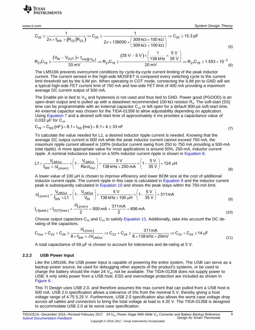
2.2.2 USB Power InputLike the LM5166, the USB power input is capable of powering the entire system. The USB can serve as abackup power source, be used for debugging other aspects of the product's systems, or be used tocharge the battery should the main 24 VAC not be available. The TIDA-01358 does not supply power toUSB; it only sinks power from a USB host. ESD and overvoltage protection are included as shown inFigure 6.
This TI Design uses USB 2.0, and therefore assumes the max current that can pulled from a USB host is500 mA. USB 2.0 specification allows a tolerance of 5% from the nominal 5 V, thereby giving a hostvoltage range of 4.75 5.25 V. Furthermore, USB 2.0 specification also allows the worst case voltage dropacross all cables and connectors to bring the total voltage at load to 4.35 V. The TIDA-01358 is designedto accommodate USB 2.0 at its worst case specification.
U3-P
U3-N
LMOut
R6
33.2 kΩ
U4-P
U4-N
USBIn
R9
33.2 kΩ
OUT (PWRin)
Load
U3
U4
TPS27081A
TPS27081A
C4
47 pF
R7
2 kΩ
USBInR24
20 kΩ
R26
20 kΩ
R25
20 kΩ
R27
22.1 kΩ
USBIn LMOut
LM2903
U7
R28
200 kΩ
C29
15 nF
NC1
NC2
IO13
GND4
IO25
U1
TPD2E2U06DRLR
GND
0.1µFC22
GND
11
22
U8TPD1E10B06DPYR
GND
1.00R29
GND
USBIn
4.7µFC21
1
2
3
4
5
6
7
8
9
J1
ZX62WRD-B-5PCGNDGND
D-
D+
Copyright © 2016, Texas Instruments Incorporated
System Design Theory www.ti.com
10 TIDUCE1A–December 2016–Revised February 2017Submit Documentation Feedback
Copyright © 2016–2017, Texas Instruments Incorporated
24-VAC Power Stage With Wide VIN Converter and Battery Backup ReferenceDesign for Smart Thermostat
R29and C21 provide a snubber circuit to the USB Vbus, reducing the overshoot and ringing caused thecable inductance and capacitive load resonance. The snubber circuit must be tuned for each systemdesign; therefore, the snubber component values used in the TIDA-01358 must be tested when designedinto a new system and the values must be changed appropriately. The ORing circuit used in this TI Designhas a maximum input voltage rating of 8 V, so the USB voltage must remain below that threshold andwithin USB specifications.
Figure 6. USB Implementation
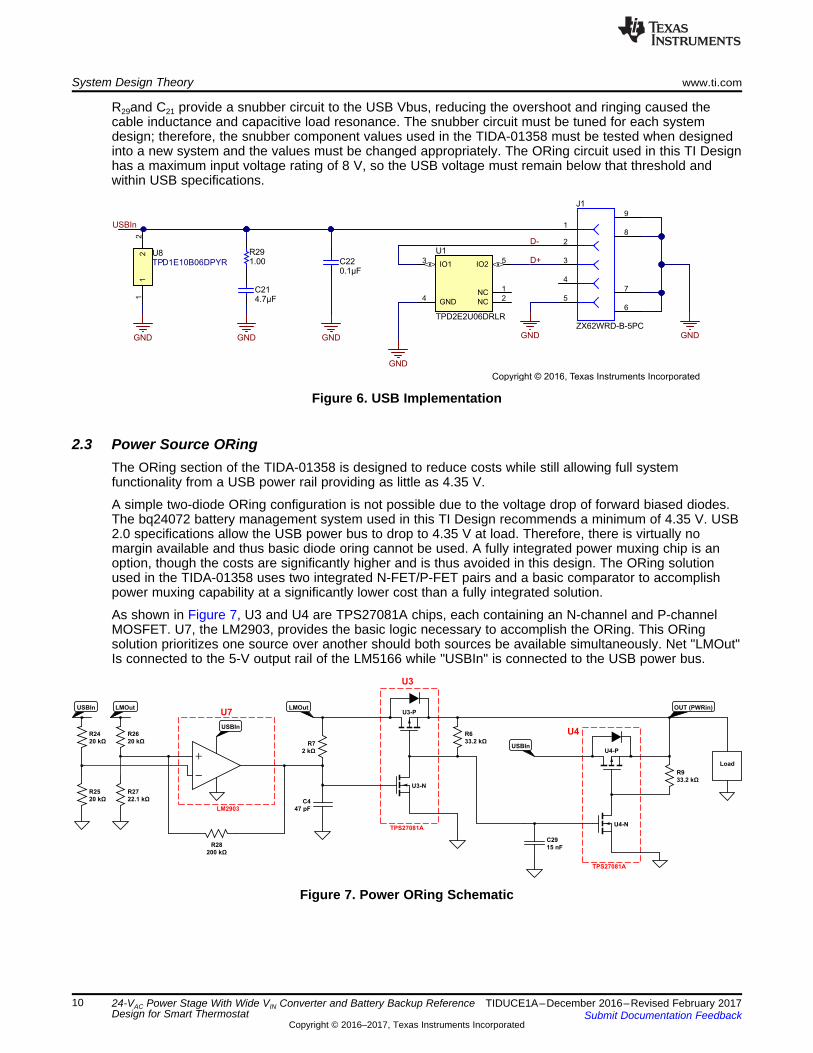
2.3 Power Source ORingThe ORing section of the TIDA-01358 is designed to reduce costs while still allowing full systemfunctionality from a USB power rail providing as little as 4.35 V.
A simple two-diode ORing configuration is not possible due to the voltage drop of forward biased diodes.The bq24072 battery management system used in this TI Design recommends a minimum of 4.35 V. USB2.0 specifications allow the USB power bus to drop to 4.35 V at load. Therefore, there is virtually nomargin available and thus basic diode oring cannot be used. A fully integrated power muxing chip is anoption, though the costs are significantly higher and is thus avoided in this design. The ORing solutionused in the TIDA-01358 uses two integrated N-FET/P-FET pairs and a basic comparator to accomplishpower muxing capability at a significantly lower cost than a fully integrated solution.
As shown in Figure 7, U3 and U4 are TPS27081A chips, each containing an N-channel and P-channelMOSFET. U7, the LM2903, provides the basic logic necessary to accomplish the ORing. This ORingsolution prioritizes one source over another should both sources be available simultaneously. Net "LMOut"Is connected to the 5-V output rail of the LM5166 while "USBIn" is connected to the USB power bus.
Figure 7. Power ORing Schematic
U3-P
U3-N
LMOut
R6
33.2 kΩ
U4-P
U4-N
USBIn
R9
33.2 kΩ
OUT (PWRin)
Load
U3
U4
TPS27081A
TPS27081A
C4
47 pF
R7
2 kΩ
USBInR24
20 kΩ
R26
20 kΩ
R25
20 kΩ
R27
22.1 kΩ
USBIn LMOut
LM2903
U7
R28
200 kΩ
C29
15 nF
5 V 0 V
U7+ < U7- 0 V
0 V
0 V
U3-N Off
U3-P Off
5 V
U4-P On
U4-N On
0 V
5 V
5 V 5 V
U3-P
U3-N
LMOut
R6
33.2 kΩ
U4-P
U4-N
USBIn
R9
33.2 kΩ
OUT (PWRin)
Load
U3
U4
TPS27081A
TPS27081A
C4
47 pF
R7
2 kΩ
USBInR24
20 kΩ
R26
20 kΩ
R25
20 kΩ
R27
22.1 kΩ
USBIn LMOut
LM2903
U7
R28
200 kΩ
C29
15 nF
0 to 5.2 V 5 V
U7+ > U7- Hi-Z
5 V
5 V
U3-N On
5 V
U3-P On
0 to 5.2 V
U4-N Off
U4-N Off
0 V
5 V
0 V
www.ti.com System Design Theory
11TIDUCE1A–December 2016–Revised February 2017Submit Documentation Feedback
Copyright © 2016–2017, Texas Instruments Incorporated
24-VAC Power Stage With Wide VIN Converter and Battery Backup ReferenceDesign for Smart Thermostat
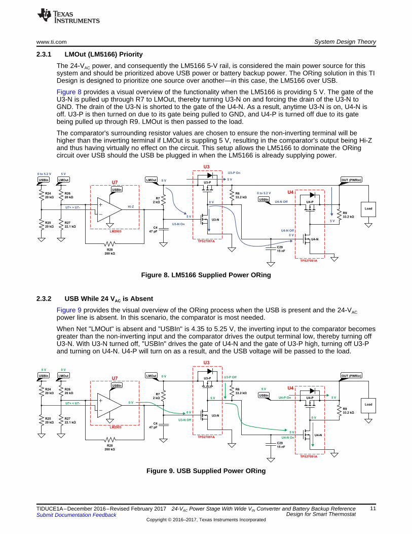
2.3.1 LMOut (LM5166) PriorityThe 24-VAC power, and consequently the LM5166 5-V rail, is considered the main power source for thissystem and should be prioritized above USB power or battery backup power. The ORing solution in this TIDesign is designed to prioritize one source over another—in this case, the LM5166 over USB.
Figure 8 provides a visual overview of the functionality when the LM5166 is providing 5 V. The gate of theU3-N is pulled up through R7 to LMOut, thereby turning U3-N on and forcing the drain of the U3-N toGND. The drain of the U3-N is shorted to the gate of the U4-N. As a result, anytime U3-N is on, U4-N isoff. U3-P is then turned on due to its gate being pulled to GND, and U4-P is turned off due to its gatebeing pulled up through R9. LMOut is then passed to the load.
The comparator's surrounding resistor values are chosen to ensure the non-inverting terminal will behigher than the inverting terminal if LMOut is suppling 5 V, resulting in the comparator's output being Hi-Zand thus having virtually no effect on the circuit. This setup allows the LM5166 to dominate the ORingcircuit over USB should the USB be plugged in when the LM5166 is already supplying power.
Figure 8. LM5166 Supplied Power ORing
2.3.2 USB While 24 VAC is AbsentFigure 9 provides the visual overview of the ORing process when the USB is present and the 24-VACpower line is absent. In this scenario, the comparator is most needed.
When Net "LMOut" is absent and "USBIn" is 4.35 to 5.25 V, the inverting input to the comparator becomesgreater than the non-inverting input and the comparator drives the output terminal low, thereby turning offU3-N. With U3-N turned off, "USBIn" drives the gate of U4-N and the gate of U3-P high, turning off U3-Pand turning on U4-N. U4-P will turn on as a result, and the USB voltage will be passed to the load.
Figure 9. USB Supplied Power ORing
eqL 26HZR
eqL
R R 19.9 k 20 kLMOut IN 2.5 V 5.01V
R 19.9 k
æ ö æ öW + W= - ´ = ´ =ç ÷ ç ÷ç ÷ Wè øè ø
eqL
22.1k 200 kR 19.9 k
22.1k 200 k
W ´ W= = W
W + W
LRUSBIn 2 IN LR 2 2.74 V 5.48 V= ´ + = ´ =
27
27 eqH
R 22.1kIN LR LMOut 5 V 2.74 V
R R 22.1k 18.18 k
æ ö æ öW+ = ´ = ´ =ç ÷ ç ÷ç ÷+ W + Wè øè ø
eqH
20 k 200 kR 18.18 k
20 k 200 k
W ´ W= = W
W + W
System Design Theory www.ti.com
12 TIDUCE1A–December 2016–Revised February 2017Submit Documentation Feedback
Copyright © 2016–2017, Texas Instruments Incorporated
24-VAC Power Stage With Wide VIN Converter and Battery Backup ReferenceDesign for Smart Thermostat
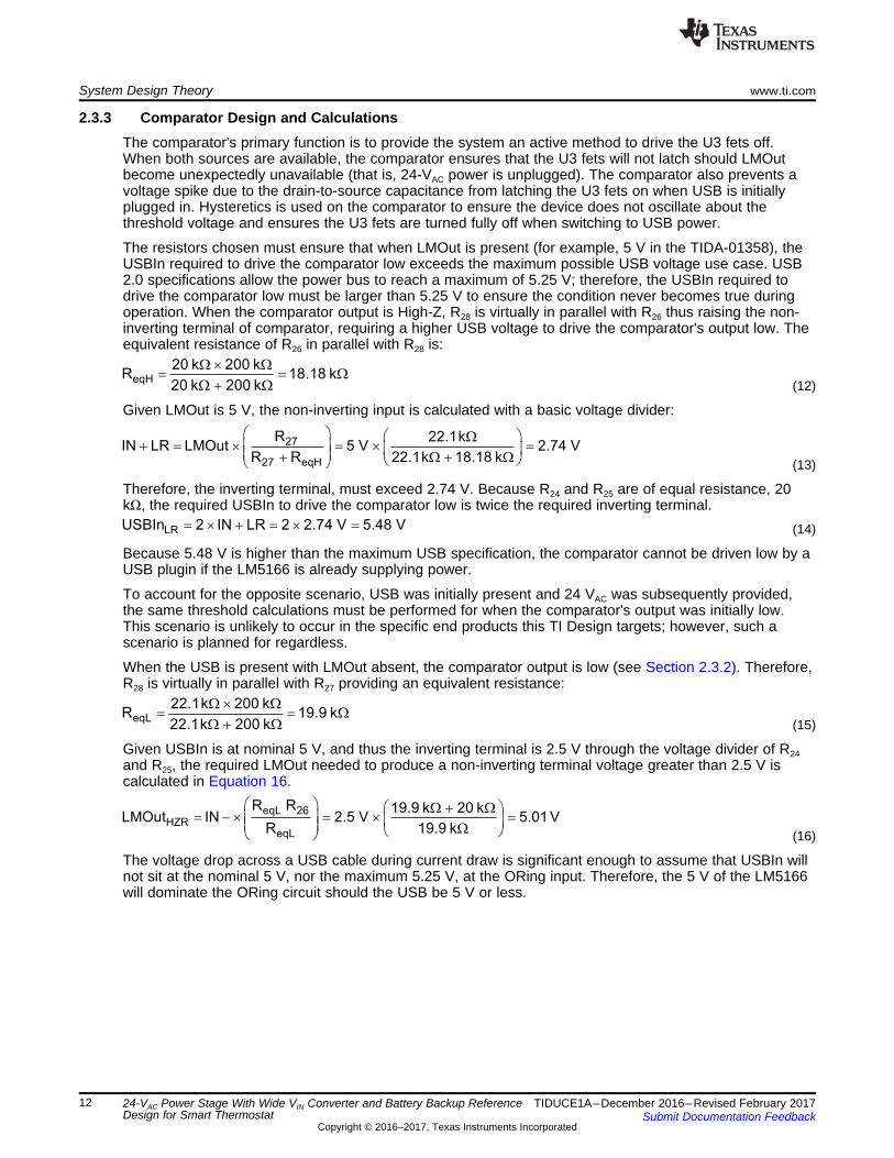
2.3.3 Comparator Design and CalculationsThe comparator's primary function is to provide the system an active method to drive the U3 fets off.When both sources are available, the comparator ensures that the U3 fets will not latch should LMOutbecome unexpectedly unavailable (that is, 24-VAC power is unplugged). The comparator also prevents avoltage spike due to the drain-to-source capacitance from latching the U3 fets on when USB is initiallyplugged in. Hysteretics is used on the comparator to ensure the device does not oscillate about thethreshold voltage and ensures the U3 fets are turned fully off when switching to USB power.
The resistors chosen must ensure that when LMOut is present (for example, 5 V in the TIDA-01358), theUSBIn required to drive the comparator low exceeds the maximum possible USB voltage use case. USB2.0 specifications allow the power bus to reach a maximum of 5.25 V; therefore, the USBIn required todrive the comparator low must be larger than 5.25 V to ensure the condition never becomes true duringoperation. When the comparator output is High-Z, R28 is virtually in parallel with R26 thus raising the non-inverting terminal of comparator, requiring a higher USB voltage to drive the comparator's output low. Theequivalent resistance of R26 in parallel with R28 is:
(12)
Given LMOut is 5 V, the non-inverting input is calculated with a basic voltage divider:
(13)
Therefore, the inverting terminal, must exceed 2.74 V. Because R24 and R25 are of equal resistance, 20kΩ, the required USBIn to drive the comparator low is twice the required inverting terminal.
(14)
Because 5.48 V is higher than the maximum USB specification, the comparator cannot be driven low by aUSB plugin if the LM5166 is already supplying power.
To account for the opposite scenario, USB was initially present and 24 VAC was subsequently provided,the same threshold calculations must be performed for when the comparator's output was initially low.This scenario is unlikely to occur in the specific end products this TI Design targets; however, such ascenario is planned for regardless.
When the USB is present with LMOut absent, the comparator output is low (see Section 2.3.2). Therefore,R28 is virtually in parallel with R27 providing an equivalent resistance:
(15)
Given USBIn is at nominal 5 V, and thus the inverting terminal is 2.5 V through the voltage divider of R24and R25, the required LMOut needed to produce a non-inverting terminal voltage greater than 2.5 V iscalculated in Equation 16.
(16)
The voltage drop across a USB cable during current draw is significant enough to assume that USBIn willnot sit at the nominal 5 V, nor the maximum 5.25 V, at the ORing input. Therefore, the 5 V of the LM5166will dominate the ORing circuit should the USB be 5 V or less.
ILIM31 ILIM
IN MAX
K 1610 AR R 3 k
I 536 mA-
W= = = = W
TS1
BAT2
BAT3
CE4
EN25
EN16
PGOOD7
VSS8
CHG9
OUT10
OUT11
ILIM12
IN13
TMR14
TD15
ISET16
EP17
U5
BQ24072RGTT
GND
BMOut
GNDGND
1µFC6
GND
PWRIn
10k
R16
GND
BAT
10kR15
0
R14
GND
TS
3.0kR30
GND
DNP R15
TP10
GND
3.0kR31
4.7µFC7
4.7µFC8
0
R34
TP13
Green21
D3
100
R17
BMO1
Copyright © 2016, Texas Instruments Incorporated
www.ti.com System Design Theory
13TIDUCE1A–December 2016–Revised February 2017Submit Documentation Feedback
Copyright © 2016–2017, Texas Instruments Incorporated
24-VAC Power Stage With Wide VIN Converter and Battery Backup ReferenceDesign for Smart Thermostat
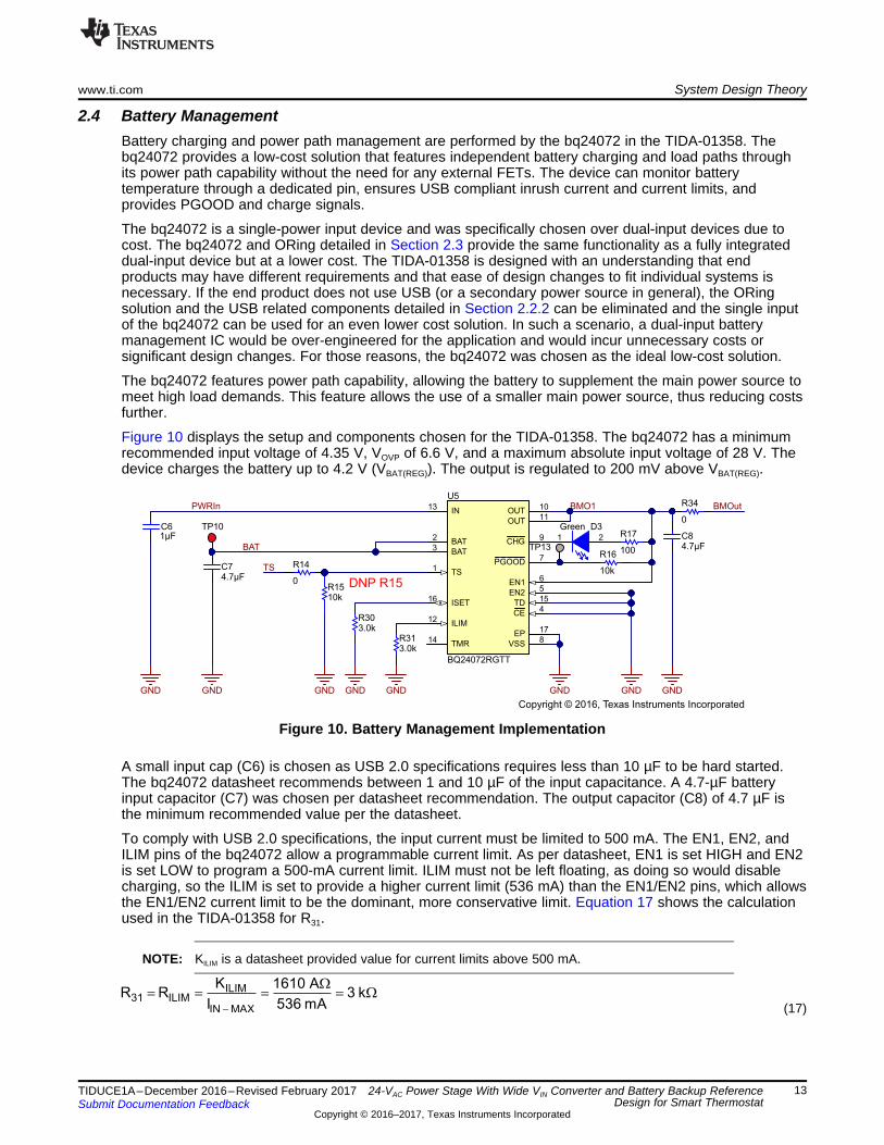
2.4 Battery ManagementBattery charging and power path management are performed by the bq24072 in the TIDA-01358. Thebq24072 provides a low-cost solution that features independent battery charging and load paths throughits power path capability without the need for any external FETs. The device can monitor batterytemperature through a dedicated pin, ensures USB compliant inrush current and current limits, andprovides PGOOD and charge signals.
The bq24072 is a single-power input device and was specifically chosen over dual-input devices due tocost. The bq24072 and ORing detailed in Section 2.3 provide the same functionality as a fully integrateddual-input device but at a lower cost. The TIDA-01358 is designed with an understanding that endproducts may have different requirements and that ease of design changes to fit individual systems isnecessary. If the end product does not use USB (or a secondary power source in general), the ORingsolution and the USB related components detailed in Section 2.2.2 can be eliminated and the single inputof the bq24072 can be used for an even lower cost solution. In such a scenario, a dual-input batterymanagement IC would be over-engineered for the application and would incur unnecessary costs orsignificant design changes. For those reasons, the bq24072 was chosen as the ideal low-cost solution.
The bq24072 features power path capability, allowing the battery to supplement the main power source tomeet high load demands. This feature allows the use of a smaller main power source, thus reducing costsfurther.
Figure 10 displays the setup and components chosen for the TIDA-01358. The bq24072 has a minimumrecommended input voltage of 4.35 V, VOVP of 6.6 V, and a maximum absolute input voltage of 28 V. Thedevice charges the battery up to 4.2 V (VBAT(REG)). The output is regulated to 200 mV above VBAT(REG).
Figure 10. Battery Management Implementation
A small input cap (C6) is chosen as USB 2.0 specifications requires less than 10 µF to be hard started.The bq24072 datasheet recommends between 1 and 10 µF of the input capacitance. A 4.7-µF batteryinput capacitor (C7) was chosen per datasheet recommendation. The output capacitor (C8) of 4.7 µF isthe minimum recommended value per the datasheet.
To comply with USB 2.0 specifications, the input current must be limited to 500 mA. The EN1, EN2, andILIM pins of the bq24072 allow a programmable current limit. As per datasheet, EN1 is set HIGH and EN2is set LOW to program a 500-mA current limit. ILIM must not be left floating, as doing so would disablecharging, so the ILIM is set to provide a higher current limit (536 mA) than the EN1/EN2 pins, which allowsthe EN1/EN2 current limit to be the dominant, more conservative limit. Equation 17 shows the calculationused in the TIDA-01358 for R31.
NOTE: KILIM is a datasheet provided value for current limits above 500 mA.
(17)
( ) ( )OUT MAX D3 Forward Bias
17
V V 4.4 V 3.2 VR 80
15 mA 15 mA
-- -= = = W
PRECHARGE CC FAST CHARGE CV TAPER DONE
Battery Voltage
Battery Current
CHG = Hi-z
VBAT(REG)
IO(CHG)
VLOWV
I(PRECHG)
I(TERM)
( )
ISET30 ISET
O CHG
K 890 AR R 3 k
I 300 mA
W= = = @ W
System Design Theory www.ti.com
14 TIDUCE1A–December 2016–Revised February 2017Submit Documentation Feedback
Copyright © 2016–2017, Texas Instruments Incorporated
24-VAC Power Stage With Wide VIN Converter and Battery Backup ReferenceDesign for Smart Thermostat
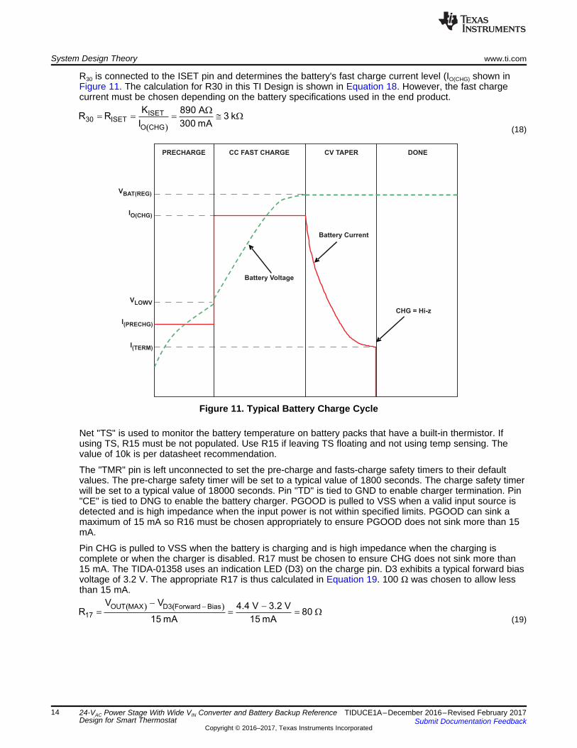
R30 is connected to the ISET pin and determines the battery's fast charge current level (IO(CHG) shown inFigure 11. The calculation for R30 in this TI Design is shown in Equation 18. However, the fast chargecurrent must be chosen depending on the battery specifications used in the end product.
(18)
Figure 11. Typical Battery Charge Cycle
Net "TS" is used to monitor the battery temperature on battery packs that have a built-in thermistor. Ifusing TS, R15 must be not populated. Use R15 if leaving TS floating and not using temp sensing. Thevalue of 10k is per datasheet recommendation.
The "TMR" pin is left unconnected to set the pre-charge and fasts-charge safety timers to their defaultvalues. The pre-charge safety timer will be set to a typical value of 1800 seconds. The charge safety timerwill be set to a typical value of 18000 seconds. Pin "TD" is tied to GND to enable charger termination. Pin"CE" is tied to DNG to enable the battery charger. PGOOD is pulled to VSS when a valid input source isdetected and is high impedance when the input power is not within specified limits. PGOOD can sink amaximum of 15 mA so R16 must be chosen appropriately to ensure PGOOD does not sink more than 15mA.
Pin CHG is pulled to VSS when the battery is charging and is high impedance when the charging iscomplete or when the charger is disabled. R17 must be chosen to ensure CHG does not sink more than15 mA. The TIDA-01358 uses an indication LED (D3) on the charge pin. D3 exhibits a typical forward biasvoltage of 3.2 V. The appropriate R17 is thus calculated in Equation 19. 100 Ω was chosen to allow lessthan 15 mA.
(19)
OUT
INOUT
SW L
V 3.3 V1 1
V 4.4 VL V 3.3 V 1.03 H 1 H
F I 2 MHz 0.4
æ ö æ ö- -ç ÷ ç ÷ç ÷ ç ÷= ´ = ´ = m @ m
´ D ´ç ÷ ç ÷ç ÷ç ÷ è øè ø
LL,MAX OUT,MAX
I 0.4 AI I 1A 1.2 A
2 2
D= + = + =
EN1
GND2
GND3
FB4
VOS5
PG6
SW7
VIN8
PAD9
U6
TLV62080DSGR
BMOut
39.2kR20
249kR19
GND
22µFC10
1µH
L2
GND GNDGND
178k
R18
3V3
TP9
TP11
TP8
10µFC9
0
R33 3V3SW
Copyright © 2016, Texas Instruments Incorporated
www.ti.com System Design Theory
15TIDUCE1A–December 2016–Revised February 2017Submit Documentation Feedback
Copyright © 2016–2017, Texas Instruments Incorporated
24-VAC Power Stage With Wide VIN Converter and Battery Backup ReferenceDesign for Smart Thermostat
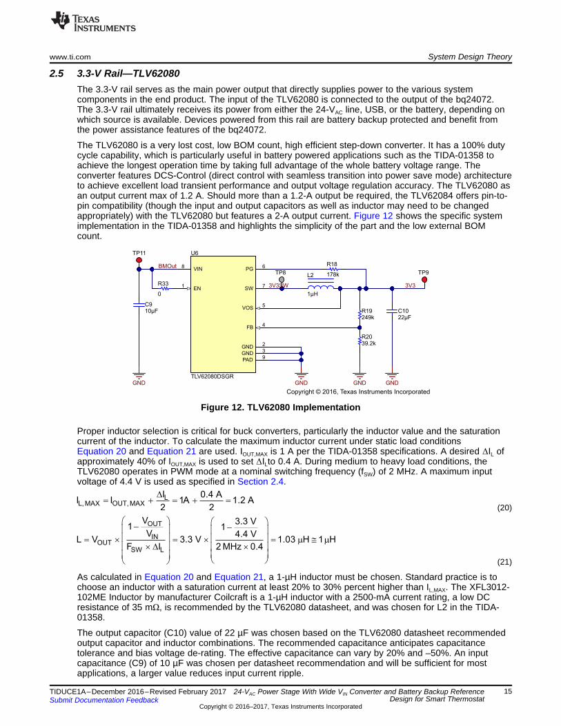
2.5 3.3-V Rail—TLV62080The 3.3-V rail serves as the main power output that directly supplies power to the various systemcomponents in the end product. The input of the TLV62080 is connected to the output of the bq24072.The 3.3-V rail ultimately receives its power from either the 24-VAC line, USB, or the battery, depending onwhich source is available. Devices powered from this rail are battery backup protected and benefit fromthe power assistance features of the bq24072.
The TLV62080 is a very lost cost, low BOM count, high efficient step-down converter. It has a 100% dutycycle capability, which is particularly useful in battery powered applications such as the TIDA-01358 toachieve the longest operation time by taking full advantage of the whole battery voltage range. Theconverter features DCS-Control (direct control with seamless transition into power save mode) architectureto achieve excellent load transient performance and output voltage regulation accuracy. The TLV62080 asan output current max of 1.2 A. Should more than a 1.2-A output be required, the TLV62084 offers pin-to-pin compatibility (though the input and output capacitors as well as inductor may need to be changedappropriately) with the TLV62080 but features a 2-A output current. Figure 12 shows the specific systemimplementation in the TIDA-01358 and highlights the simplicity of the part and the low external BOMcount.
Figure 12. TLV62080 Implementation
Proper inductor selection is critical for buck converters, particularly the inductor value and the saturationcurrent of the inductor. To calculate the maximum inductor current under static load conditionsEquation 20 and Equation 21 are used. IOUT,MAX is 1 A per the TIDA-01358 specifications. A desired ΔIL ofapproximately 40% of IOUT,MAX is used to set ΔILto 0.4 A. During medium to heavy load conditions, theTLV62080 operates in PWM mode at a nominal switching frequency (fSW) of 2 MHz. A maximum inputvoltage of 4.4 V is used as specified in Section 2.4.
(20)
(21)
As calculated in Equation 20 and Equation 21, a 1-µH inductor must be chosen. Standard practice is tochoose an inductor with a saturation current at least 20% to 30% percent higher than IL,MAX. The XFL3012-102ME Inductor by manufacturer Coilcraft is a 1-µH inductor with a 2500-mA current rating, a low DCresistance of 35 mΩ, is recommended by the TLV62080 datasheet, and was chosen for L2 in the TIDA-01358.
The output capacitor (C10) value of 22 µF was chosen based on the TLV62080 datasheet recommendedoutput capacitor and inductor combinations. The recommended capacitance anticipates capacitancetolerance and bias voltage de-rating. The effective capacitance can vary by 20% and –50%. An inputcapacitance (C9) of 10 µF was chosen per datasheet recommendation and will be sufficient for mostapplications, a larger value reduces input current ripple.

19OUT FB
20
R 249 kV V 1 0.45 V 1 3.3 V
R 39.2 k
æ ö æ öW= ´ + = ´ + =ç ÷ ç ÷
Wè øè ø
System Design Theory www.ti.com
16 TIDUCE1A–December 2016–Revised February 2017Submit Documentation Feedback
Copyright © 2016–2017, Texas Instruments Incorporated
24-VAC Power Stage With Wide VIN Converter and Battery Backup ReferenceDesign for Smart Thermostat
For best accuracy, R20 must be kept smaller than 40 kΩ to ensure that the current flowing through R20 is atleast 100 times larger than IFB. Using Equation 22, a desired output voltage of 3.3 V, a datasheet specifiedfeedback regulation voltage of 0.45 V, and a chosen R20 value of 39.2 kΩ, R19 is calculated to be 249 kΩ.As with most applications, tight tolerance resistors (less than or equal to 1%) should be used for thefeedback network.
(22)
VOS serves as the output voltage sense terminal for the internal control loop and must be connected tothe output.
Barrel wireGND
Scope probe
Current carrying wires
www.ti.com Getting Started Hardware
17TIDUCE1A–December 2016–Revised February 2017Submit Documentation Feedback
Copyright © 2016–2017, Texas Instruments Incorporated
24-VAC Power Stage With Wide VIN Converter and Battery Backup ReferenceDesign for Smart Thermostat
3 Getting Started Hardware
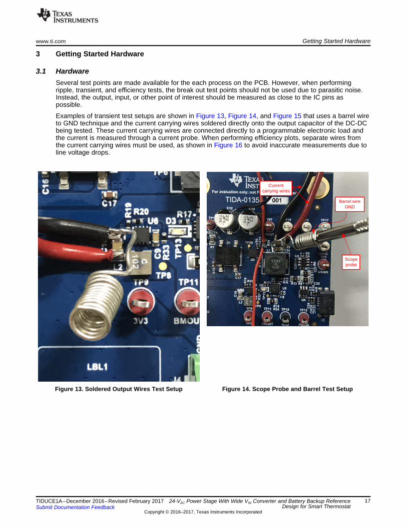
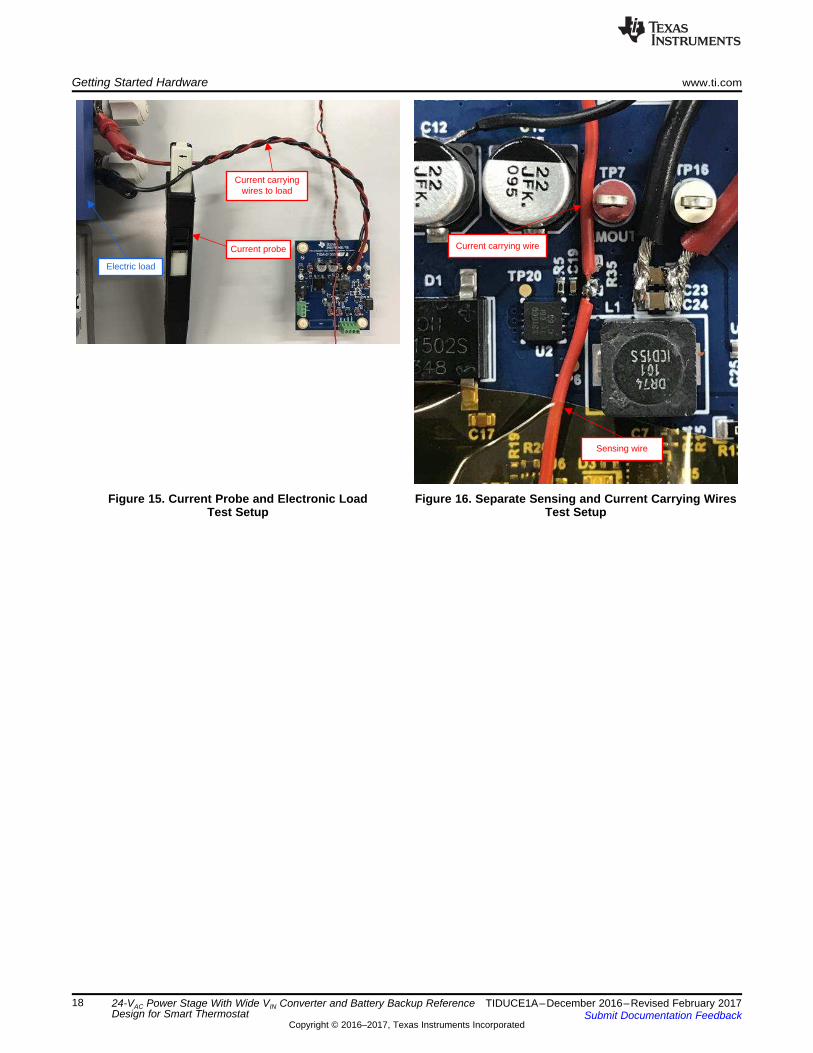
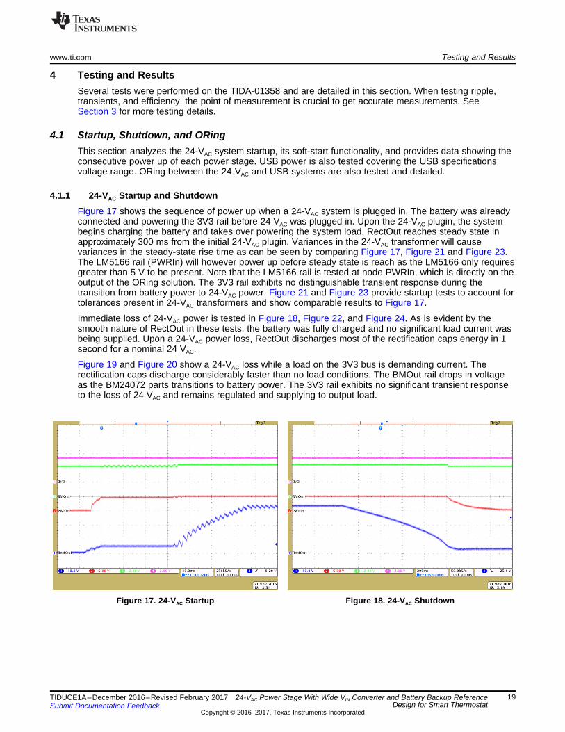
3.1 HardwareSeveral test points are made available for the each process on the PCB. However, when performingripple, transient, and efficiency tests, the break out test points should not be used due to parasitic noise.Instead, the output, input, or other point of interest should be measured as close to the IC pins aspossible.
Examples of transient test setups are shown in Figure 13, Figure 14, and Figure 15 that uses a barrel wireto GND technique and the current carrying wires soldered directly onto the output capacitor of the DC-DCbeing tested. These current carrying wires are connected directly to a programmable electronic load andthe current is measured through a current probe. When performing efficiency plots, separate wires fromthe current carrying wires must be used, as shown in Figure 16 to avoid inaccurate measurements due toline voltage drops.
Figure 13. Soldered Output Wires Test Setup Figure 14. Scope Probe and Barrel Test Setup
Current carrying wire
Sensing wire
Current carrying wires to load
Current probe
Electric load
Getting Started Hardware www.ti.com
18 TIDUCE1A–December 2016–Revised February 2017Submit Documentation Feedback
Copyright © 2016–2017, Texas Instruments Incorporated
24-VAC Power Stage With Wide VIN Converter and Battery Backup ReferenceDesign for Smart Thermostat
Figure 15. Current Probe and Electronic LoadTest Setup
Figure 16. Separate Sensing and Current Carrying WiresTest Setup
www.ti.com Testing and Results
19TIDUCE1A–December 2016–Revised February 2017Submit Documentation Feedback
Copyright © 2016–2017, Texas Instruments Incorporated
24-VAC Power Stage With Wide VIN Converter and Battery Backup ReferenceDesign for Smart Thermostat
4 Testing and ResultsSeveral tests were performed on the TIDA-01358 and are detailed in this section. When testing ripple,transients, and efficiency, the point of measurement is crucial to get accurate measurements. SeeSection 3 for more testing details.
4.1 Startup, Shutdown, and ORingThis section analyzes the 24-VAC system startup, its soft-start functionality, and provides data showing theconsecutive power up of each power stage. USB power is also tested covering the USB specificationsvoltage range. ORing between the 24-VAC and USB systems are also tested and detailed.
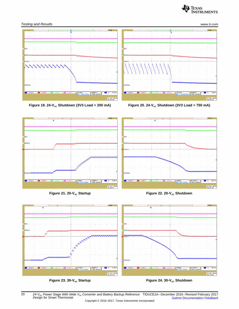
4.1.1 24-VAC Startup and ShutdownFigure 17 shows the sequence of power up when a 24-VAC system is plugged in. The battery was alreadyconnected and powering the 3V3 rail before 24 VAC was plugged in. Upon the 24-VAC plugin, the systembegins charging the battery and takes over powering the system load. RectOut reaches steady state inapproximately 300 ms from the initial 24-VAC plugin. Variances in the 24-VAC transformer will causevariances in the steady-state rise time as can be seen by comparing Figure 17, Figure 21 and Figure 23.The LM5166 rail (PWRIn) will however power up before steady state is reach as the LM5166 only requiresgreater than 5 V to be present. Note that the LM5166 rail is tested at node PWRIn, which is directly on theoutput of the ORing solution. The 3V3 rail exhibits no distinguishable transient response during thetransition from battery power to 24-VAC power. Figure 21 and Figure 23 provide startup tests to account fortolerances present in 24-VAC transformers and show comparable results to Figure 17.
Immediate loss of 24-VAC power is tested in Figure 18, Figure 22, and Figure 24. As is evident by thesmooth nature of RectOut in these tests, the battery was fully charged and no significant load current wasbeing supplied. Upon a 24-VAC power loss, RectOut discharges most of the rectification caps energy in 1second for a nominal 24 VAC.
Figure 19 and Figure 20 show a 24-VAC loss while a load on the 3V3 bus is demanding current. Therectification caps discharge considerably faster than no load conditions. The BMOut rail drops in voltageas the BM24072 parts transitions to battery power. The 3V3 rail exhibits no significant transient responseto the loss of 24 VAC and remains regulated and supplying to output load.
Figure 17. 24-VAC Startup Figure 18. 24-VAC Shutdown
Testing and Results www.ti.com
20 TIDUCE1A–December 2016–Revised February 2017Submit Documentation Feedback
Copyright © 2016–2017, Texas Instruments Incorporated
24-VAC Power Stage With Wide VIN Converter and Battery Backup ReferenceDesign for Smart Thermostat
Figure 19. 24-VAC Shutdown (3V3 Load = 200 mA) Figure 20. 24-VAC Shutdown (3V3 Load = 750 mA)
Figure 21. 20-VAC Startup Figure 22. 20-VAC Shutdown
Figure 23. 30-VAC Startup Figure 24. 30-VAC Shutdown
www.ti.com Testing and Results
21TIDUCE1A–December 2016–Revised February 2017Submit Documentation Feedback
Copyright © 2016–2017, Texas Instruments Incorporated
24-VAC Power Stage With Wide VIN Converter and Battery Backup ReferenceDesign for Smart Thermostat
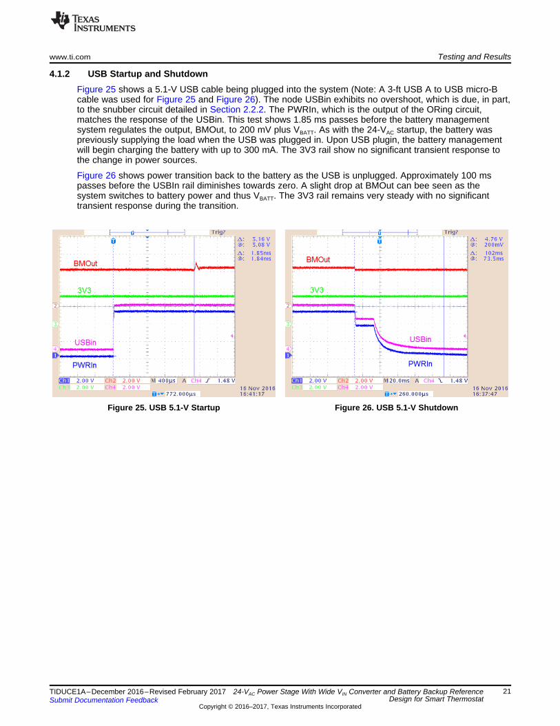
4.1.2 USB Startup and ShutdownFigure 25 shows a 5.1-V USB cable being plugged into the system (Note: A 3-ft USB A to USB micro-Bcable was used for Figure 25 and Figure 26). The node USBin exhibits no overshoot, which is due, in part,to the snubber circuit detailed in Section 2.2.2. The PWRIn, which is the output of the ORing circuit,matches the response of the USBin. This test shows 1.85 ms passes before the battery managementsystem regulates the output, BMOut, to 200 mV plus VBATT. As with the 24-VAC startup, the battery waspreviously supplying the load when the USB was plugged in. Upon USB plugin, the battery managementwill begin charging the battery with up to 300 mA. The 3V3 rail show no significant transient response tothe change in power sources.
Figure 26 shows power transition back to the battery as the USB is unplugged. Approximately 100 mspasses before the USBIn rail diminishes towards zero. A slight drop at BMOut can bee seen as thesystem switches to battery power and thus VBATT. The 3V3 rail remains very steady with no significanttransient response during the transition.
Figure 25. USB 5.1-V Startup Figure 26. USB 5.1-V Shutdown
Testing and Results www.ti.com
22 TIDUCE1A–December 2016–Revised February 2017Submit Documentation Feedback
Copyright © 2016–2017, Texas Instruments Incorporated
24-VAC Power Stage With Wide VIN Converter and Battery Backup ReferenceDesign for Smart Thermostat
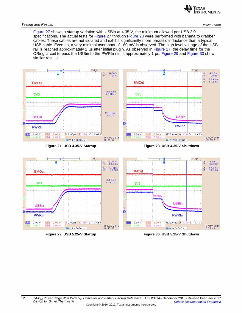
Figure 27 shows a startup variation with USBin at 4.35 V, the minimum allowed per USB 2.0specifications. The actual tests for Figure 27 through Figure 28 were performed with banana to grabbercables. These cables are not isolated and exhibit significantly more parasitic inductance than a typicalUSB cable. Even so, a very minimal overshoot of 160 mV is observed. The high level voltage of the USBrail is reached approximately 2 µs after initial plugin. As observed in Figure 27, the delay time for theORing circuit to pass the USBin to the PWRIn rail is approximately 1 µs. Figure 29 and Figure 30 showsimilar results.
Figure 27. USB 4.35-V Startup Figure 28. USB 4.35-V Shutdown
Figure 29. USB 5.25-V Startup Figure 30. USB 5.25-V Shutdown
www.ti.com Testing and Results
23TIDUCE1A–December 2016–Revised February 2017Submit Documentation Feedback
Copyright © 2016–2017, Texas Instruments Incorporated
24-VAC Power Stage With Wide VIN Converter and Battery Backup ReferenceDesign for Smart Thermostat
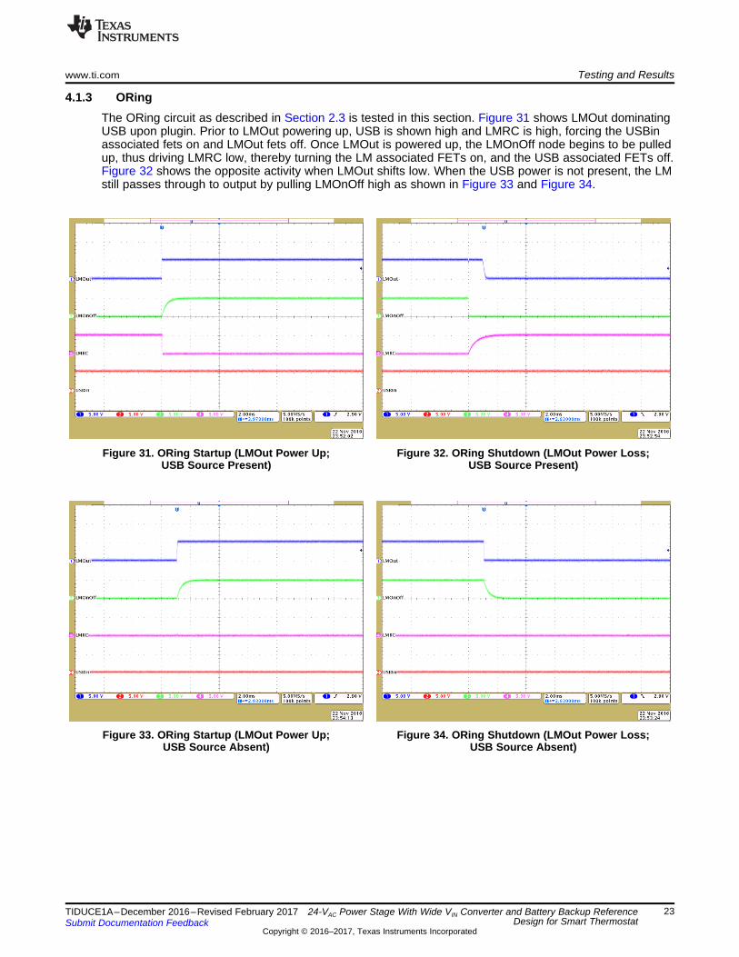
4.1.3 ORingThe ORing circuit as described in Section 2.3 is tested in this section. Figure 31 shows LMOut dominatingUSB upon plugin. Prior to LMOut powering up, USB is shown high and LMRC is high, forcing the USBinassociated fets on and LMOut fets off. Once LMOut is powered up, the LMOnOff node begins to be pulledup, thus driving LMRC low, thereby turning the LM associated FETs on, and the USB associated FETs off.Figure 32 shows the opposite activity when LMOut shifts low. When the USB power is not present, the LMstill passes through to output by pulling LMOnOff high as shown in Figure 33 and Figure 34.
Figure 31. ORing Startup (LMOut Power Up;USB Source Present)
Figure 32. ORing Shutdown (LMOut Power Loss;USB Source Present)
Figure 33. ORing Startup (LMOut Power Up;USB Source Absent)
Figure 34. ORing Shutdown (LMOut Power Loss;USB Source Absent)
Testing and Results www.ti.com
24 TIDUCE1A–December 2016–Revised February 2017Submit Documentation Feedback
Copyright © 2016–2017, Texas Instruments Incorporated
24-VAC Power Stage With Wide VIN Converter and Battery Backup ReferenceDesign for Smart Thermostat
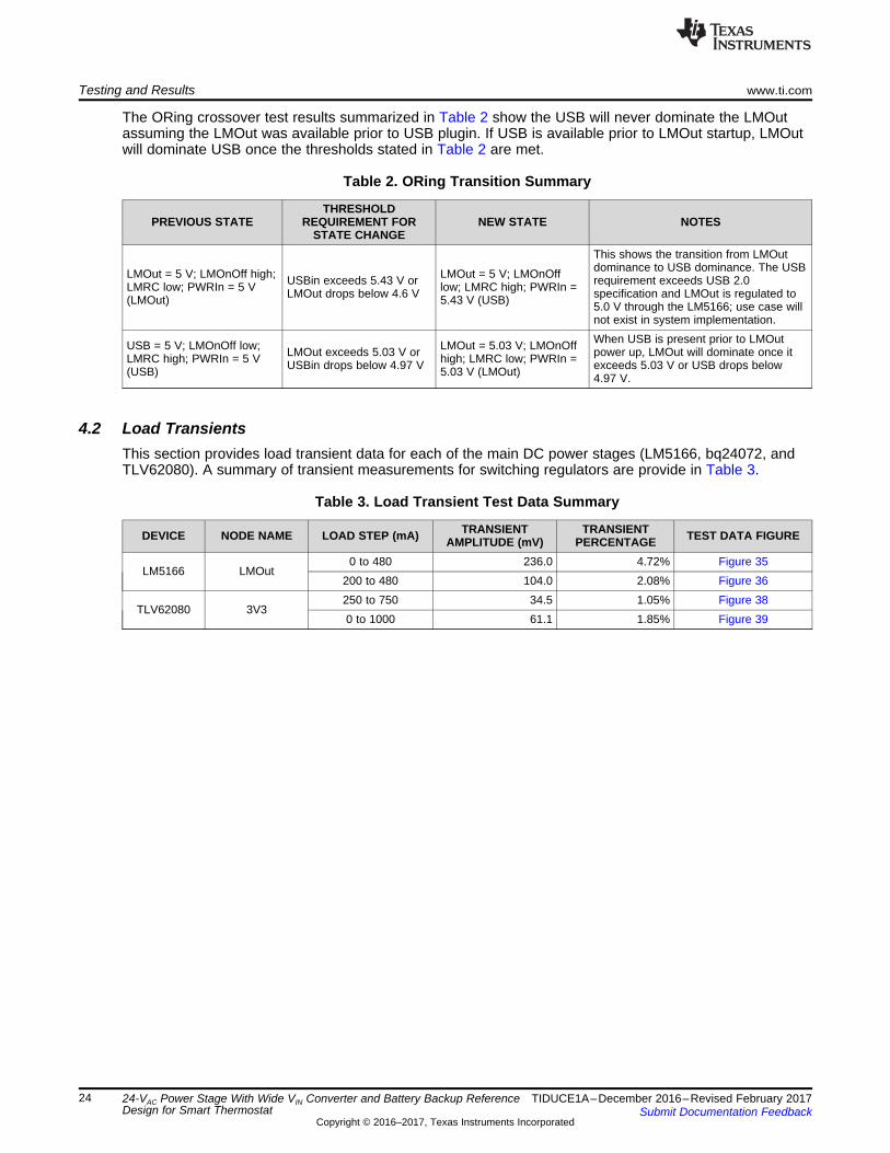
The ORing crossover test results summarized in Table 2 show the USB will never dominate the LMOutassuming the LMOut was available prior to USB plugin. If USB is available prior to LMOut startup, LMOutwill dominate USB once the thresholds stated in Table 2 are met.
Table 2. ORing Transition Summary
PREVIOUS STATETHRESHOLD
REQUIREMENT FORSTATE CHANGE
NEW STATE NOTES
LMOut = 5 V; LMOnOff high;LMRC low; PWRIn = 5 V(LMOut)
USBin exceeds 5.43 V orLMOut drops below 4.6 V
LMOut = 5 V; LMOnOfflow; LMRC high; PWRIn =5.43 V (USB)
This shows the transition from LMOutdominance to USB dominance. The USBrequirement exceeds USB 2.0specification and LMOut is regulated to5.0 V through the LM5166; use case willnot exist in system implementation.
USB = 5 V; LMOnOff low;LMRC high; PWRIn = 5 V(USB)
LMOut exceeds 5.03 V orUSBin drops below 4.97 V
LMOut = 5.03 V; LMOnOffhigh; LMRC low; PWRIn =5.03 V (LMOut)
When USB is present prior to LMOutpower up, LMOut will dominate once itexceeds 5.03 V or USB drops below4.97 V.
4.2 Load TransientsThis section provides load transient data for each of the main DC power stages (LM5166, bq24072, andTLV62080). A summary of transient measurements for switching regulators are provide in Table 3.
Table 3. Load Transient Test Data Summary
DEVICE NODE NAME LOAD STEP (mA) TRANSIENTAMPLITUDE (mV)
TRANSIENTPERCENTAGE TEST DATA FIGURE
LM5166 LMOut0 to 480 236.0 4.72% Figure 35
200 to 480 104.0 2.08% Figure 36
TLV62080 3V3250 to 750 34.5 1.05% Figure 380 to 1000 61.1 1.85% Figure 39
www.ti.com Testing and Results
25TIDUCE1A–December 2016–Revised February 2017Submit Documentation Feedback
Copyright © 2016–2017, Texas Instruments Incorporated
24-VAC Power Stage With Wide VIN Converter and Battery Backup ReferenceDesign for Smart Thermostat
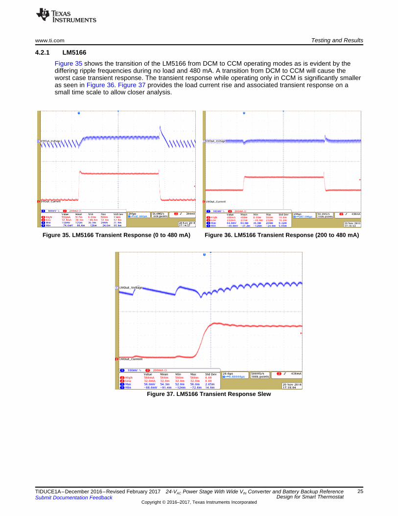
4.2.1 LM5166Figure 35 shows the transition of the LM5166 from DCM to CCM operating modes as is evident by thediffering ripple frequencies during no load and 480 mA. A transition from DCM to CCM will cause theworst case transient response. The transient response while operating only in CCM is significantly smalleras seen in Figure 36. Figure 37 provides the load current rise and associated transient response on asmall time scale to allow closer analysis.
Figure 35. LM5166 Transient Response (0 to 480 mA) Figure 36. LM5166 Transient Response (200 to 480 mA)
Figure 37. LM5166 Transient Response Slew
Testing and Results www.ti.com
26 TIDUCE1A–December 2016–Revised February 2017Submit Documentation Feedback
Copyright © 2016–2017, Texas Instruments Incorporated
24-VAC Power Stage With Wide VIN Converter and Battery Backup ReferenceDesign for Smart Thermostat
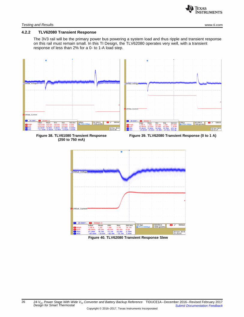
4.2.2 TLV62080 Transient ResponseThe 3V3 rail will be the primary power bus powering a system load and thus ripple and transient responseon this rail must remain small. In this TI Design, the TLV62080 operates very well, with a transientresponse of less than 2% for a 0- to 1-A load step.
Figure 38. TLV61080 Transient Response(250 to 750 mA)
Figure 39. TLV62080 Transient Response (0 to 1 A)
Figure 40. TLV62080 Transient Response Slew
www.ti.com Testing and Results
27TIDUCE1A–December 2016–Revised February 2017Submit Documentation Feedback
Copyright © 2016–2017, Texas Instruments Incorporated
24-VAC Power Stage With Wide VIN Converter and Battery Backup ReferenceDesign for Smart Thermostat
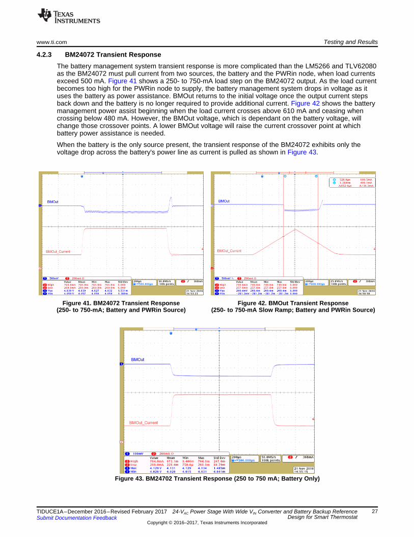
4.2.3 BM24072 Transient ResponseThe battery management system transient response is more complicated than the LM5266 and TLV62080as the BM24072 must pull current from two sources, the battery and the PWRin node, when load currentsexceed 500 mA. Figure 41 shows a 250- to 750-mA load step on the BM24072 output. As the load currentbecomes too high for the PWRin node to supply, the battery management system drops in voltage as ituses the battery as power assistance. BMOut returns to the initial voltage once the output current stepsback down and the battery is no longer required to provide additional current. Figure 42 shows the batterymanagement power assist beginning when the load current crosses above 610 mA and ceasing whencrossing below 480 mA. However, the BMOut voltage, which is dependant on the battery voltage, willchange those crossover points. A lower BMOut voltage will raise the current crossover point at whichbattery power assistance is needed.
When the battery is the only source present, the transient response of the BM24072 exhibits only thevoltage drop across the battery's power line as current is pulled as shown in Figure 43.
Figure 41. BM24072 Transient Response(250- to 750-mA; Battery and PWRin Source)
Figure 42. BMOut Transient Response(250- to 750-mA Slow Ramp; Battery and PWRin Source)
Figure 43. BM24702 Transient Response (250 to 750 mA; Battery Only)
Testing and Results www.ti.com
28 TIDUCE1A–December 2016–Revised February 2017Submit Documentation Feedback
Copyright © 2016–2017, Texas Instruments Incorporated
24-VAC Power Stage With Wide VIN Converter and Battery Backup ReferenceDesign for Smart Thermostat
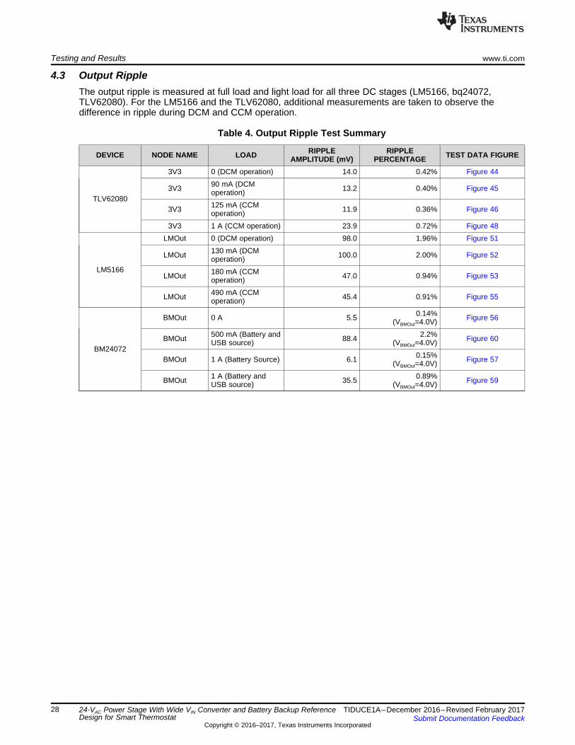
4.3 Output RippleThe output ripple is measured at full load and light load for all three DC stages (LM5166, bq24072,TLV62080). For the LM5166 and the TLV62080, additional measurements are taken to observe thedifference in ripple during DCM and CCM operation.
Table 4. Output Ripple Test Summary
DEVICE NODE NAME LOAD RIPPLEAMPLITUDE (mV)
RIPPLEPERCENTAGE TEST DATA FIGURE
TLV62080
3V3 0 (DCM operation) 14.0 0.42% Figure 44
3V3 90 mA (DCMoperation) 13.2 0.40% Figure 45
3V3 125 mA (CCMoperation) 11.9 0.36% Figure 46
3V3 1 A (CCM operation) 23.9 0.72% Figure 48
LM5166
LMOut 0 (DCM operation) 98.0 1.96% Figure 51
LMOut 130 mA (DCMoperation) 100.0 2.00% Figure 52
LMOut 180 mA (CCMoperation) 47.0 0.94% Figure 53
LMOut 490 mA (CCMoperation) 45.4 0.91% Figure 55
BM24072
BMOut 0 A 5.5 0.14%(VBMOut=4.0V) Figure 56
BMOut 500 mA (Battery andUSB source) 88.4 2.2%
(VBMOut=4.0V) Figure 60
BMOut 1 A (Battery Source) 6.1 0.15%(VBMOut=4.0V) Figure 57
BMOut 1 A (Battery andUSB source) 35.5 0.89%
(VBMOut=4.0V) Figure 59
www.ti.com Testing and Results
29TIDUCE1A–December 2016–Revised February 2017Submit Documentation Feedback
Copyright © 2016–2017, Texas Instruments Incorporated
24-VAC Power Stage With Wide VIN Converter and Battery Backup ReferenceDesign for Smart Thermostat
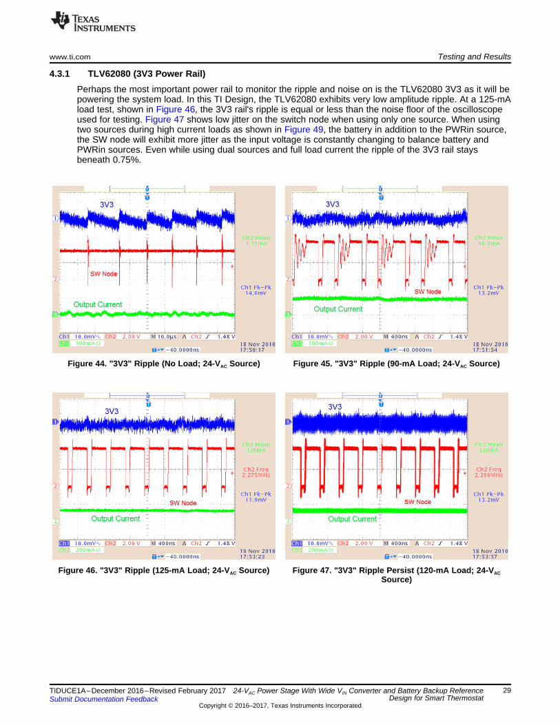
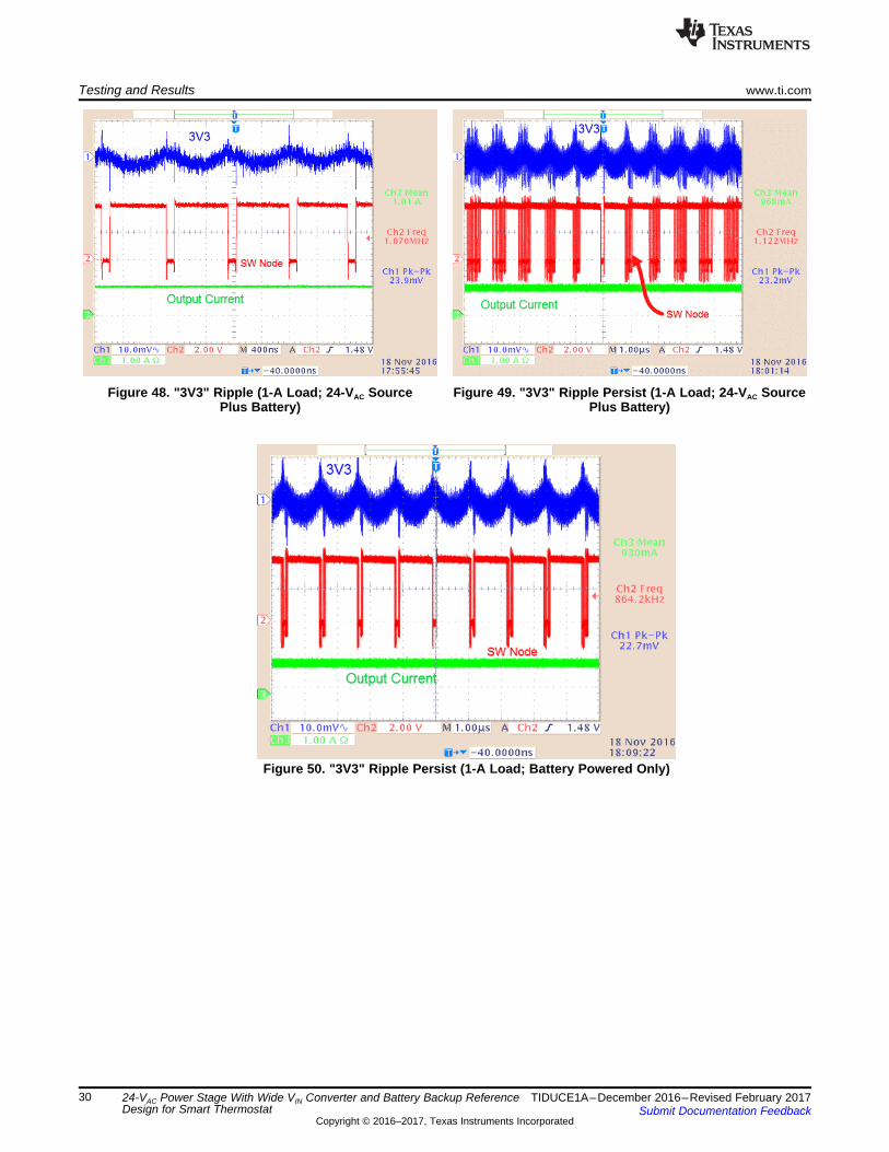
4.3.1 TLV62080 (3V3 Power Rail)Perhaps the most important power rail to monitor the ripple and noise on is the TLV62080 3V3 as it will bepowering the system load. In this TI Design, the TLV62080 exhibits very low amplitude ripple. At a 125-mAload test, shown in Figure 46, the 3V3 rail's ripple is equal or less than the noise floor of the oscilloscopeused for testing. Figure 47 shows low jitter on the switch node when using only one source. When usingtwo sources during high current loads as shown in Figure 49, the battery in addition to the PWRin source,the SW node will exhibit more jitter as the input voltage is constantly changing to balance battery andPWRin sources. Even while using dual sources and full load current the ripple of the 3V3 rail staysbeneath 0.75%.
Figure 44. "3V3" Ripple (No Load; 24-VAC Source) Figure 45. "3V3" Ripple (90-mA Load; 24-VAC Source)
Figure 46. "3V3" Ripple (125-mA Load; 24-VAC Source) Figure 47. "3V3" Ripple Persist (120-mA Load; 24-VACSource)
Testing and Results www.ti.com
30 TIDUCE1A–December 2016–Revised February 2017Submit Documentation Feedback
Copyright © 2016–2017, Texas Instruments Incorporated
24-VAC Power Stage With Wide VIN Converter and Battery Backup ReferenceDesign for Smart Thermostat
Figure 48. "3V3" Ripple (1-A Load; 24-VAC SourcePlus Battery)
Figure 49. "3V3" Ripple Persist (1-A Load; 24-VAC SourcePlus Battery)
Figure 50. "3V3" Ripple Persist (1-A Load; Battery Powered Only)
www.ti.com Testing and Results
31TIDUCE1A–December 2016–Revised February 2017Submit Documentation Feedback
Copyright © 2016–2017, Texas Instruments Incorporated
24-VAC Power Stage With Wide VIN Converter and Battery Backup ReferenceDesign for Smart Thermostat
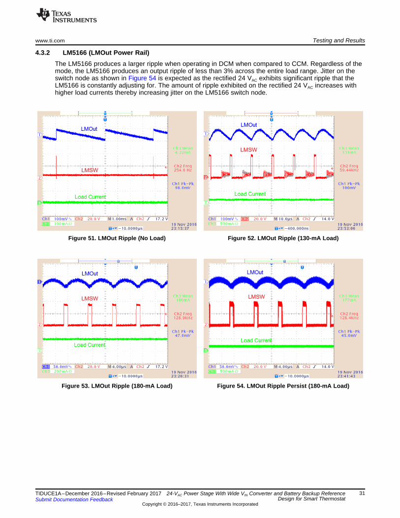
4.3.2 LM5166 (LMOut Power Rail)The LM5166 produces a larger ripple when operating in DCM when compared to CCM. Regardless of themode, the LM5166 produces an output ripple of less than 3% across the entire load range. Jitter on theswitch node as shown in Figure 54 is expected as the rectified 24 VAC exhibits significant ripple that theLM5166 is constantly adjusting for. The amount of ripple exhibited on the rectified 24 VAC increases withhigher load currents thereby increasing jitter on the LM5166 switch node.
Figure 51. LMOut Ripple (No Load) Figure 52. LMOut Ripple (130-mA Load)
Figure 53. LMOut Ripple (180-mA Load) Figure 54. LMOut Ripple Persist (180-mA Load)
Testing and Results www.ti.com
32 TIDUCE1A–December 2016–Revised February 2017Submit Documentation Feedback
Copyright © 2016–2017, Texas Instruments Incorporated
24-VAC Power Stage With Wide VIN Converter and Battery Backup ReferenceDesign for Smart Thermostat
Figure 55. LMOut Ripple (490-mA Load)
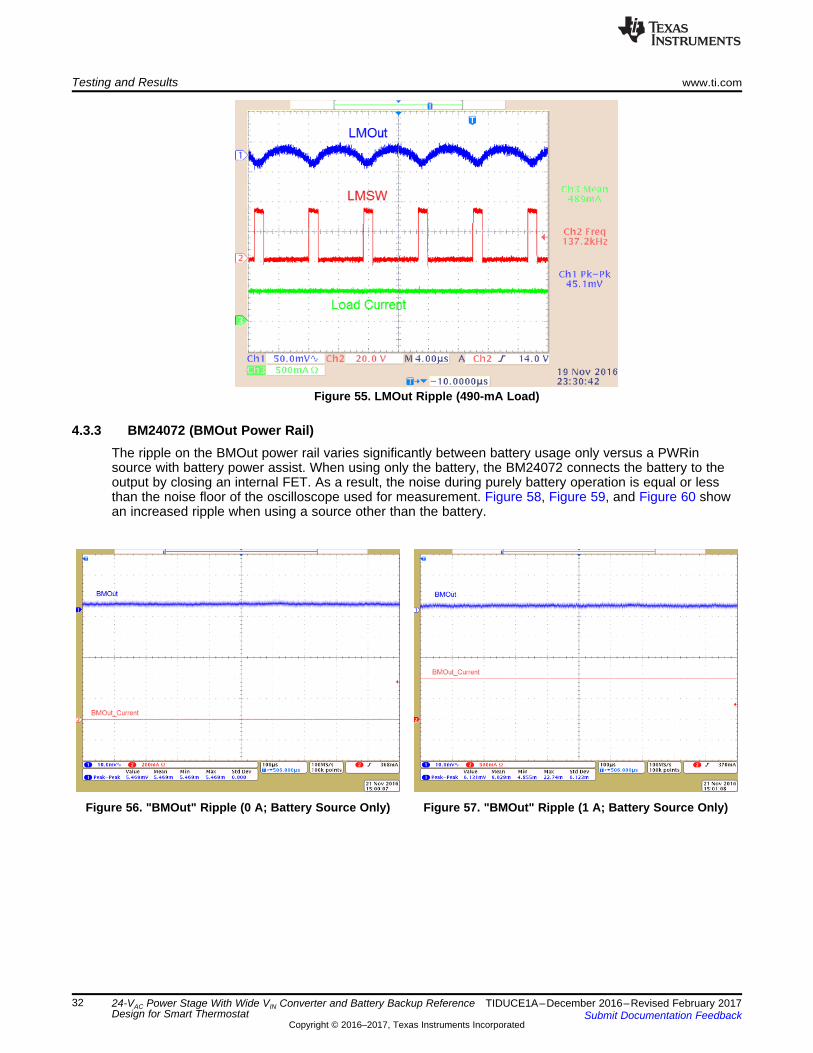
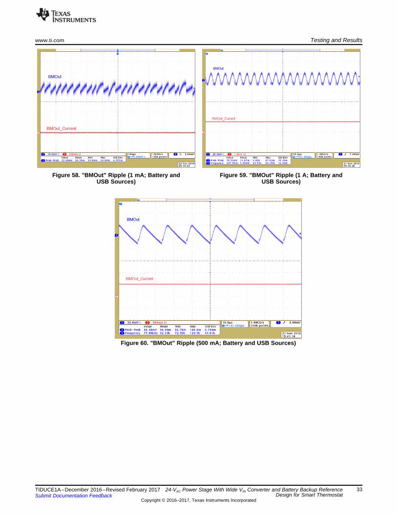
4.3.3 BM24072 (BMOut Power Rail)The ripple on the BMOut power rail varies significantly between battery usage only versus a PWRinsource with battery power assist. When using only the battery, the BM24072 connects the battery to theoutput by closing an internal FET. As a result, the noise during purely battery operation is equal or lessthan the noise floor of the oscilloscope used for measurement. Figure 58, Figure 59, and Figure 60 showan increased ripple when using a source other than the battery.
Figure 56. "BMOut" Ripple (0 A; Battery Source Only) Figure 57. "BMOut" Ripple (1 A; Battery Source Only)
www.ti.com Testing and Results
33TIDUCE1A–December 2016–Revised February 2017Submit Documentation Feedback
Copyright © 2016–2017, Texas Instruments Incorporated
24-VAC Power Stage With Wide VIN Converter and Battery Backup ReferenceDesign for Smart Thermostat
Figure 58. "BMOut" Ripple (1 mA; Battery andUSB Sources)
Figure 59. "BMOut" Ripple (1 A; Battery andUSB Sources)
Figure 60. "BMOut" Ripple (500 mA; Battery and USB Sources)
Load Current (Amps)
3V3
Bus
Vol
tage
0.001 0.01 0.1 13.316
3.317
3.318
3.319
3.32
3.321
3.322
3.323
D002
3.7 V Input4.1 V Input
Load Current (Amps)
Effi
cien
cy
Pow
er L
oss
(Wat
ts)
0.001 0.01 0.1 189% 0.00
90% 0.03
91% 0.06
92% 0.09
93% 0.12
94% 0.15
95% 0.18
96% 0.21
97% 0.24
98% 0.27
99% 0.30
D001
BATT Voltage = 3.7 VBATT Voltage = 4.1 VBATT Voltage = 3.4 V
3.7 Power Loss4.1 Power Loss3.4 Power Loss
Testing and Results www.ti.com
34 TIDUCE1A–December 2016–Revised February 2017Submit Documentation Feedback
Copyright © 2016–2017, Texas Instruments Incorporated
24-VAC Power Stage With Wide VIN Converter and Battery Backup ReferenceDesign for Smart Thermostat
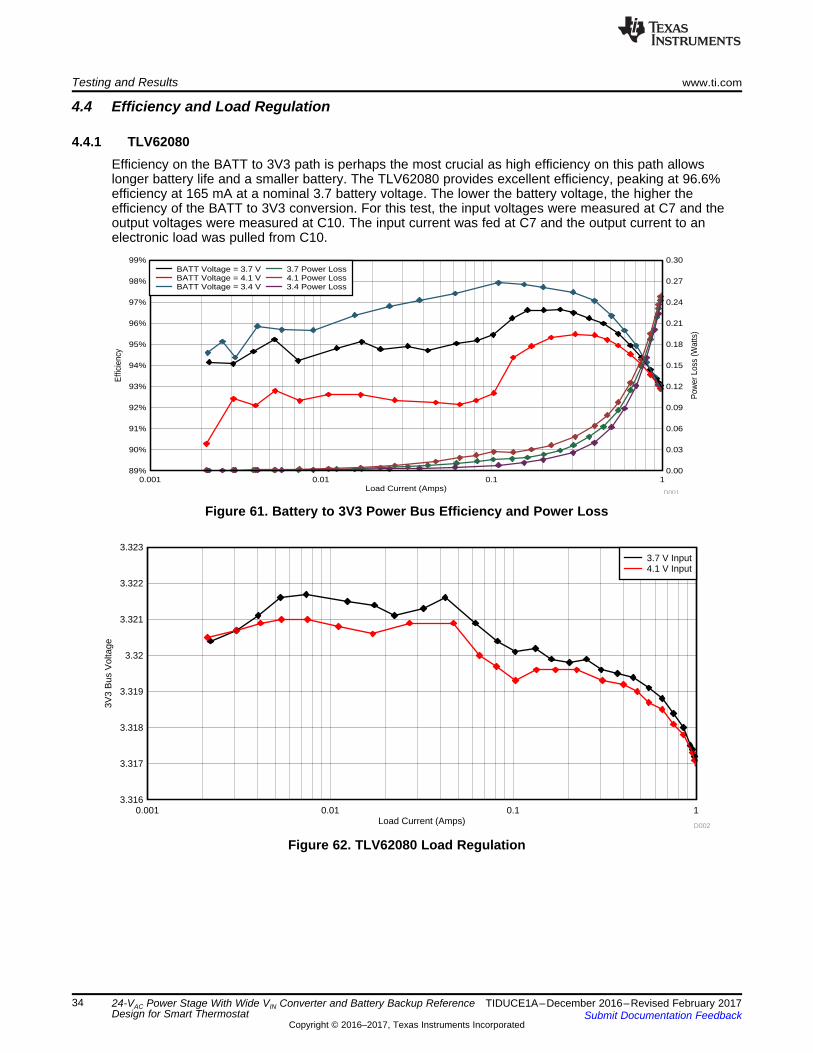
4.4 Efficiency and Load Regulation
4.4.1 TLV62080Efficiency on the BATT to 3V3 path is perhaps the most crucial as high efficiency on this path allowslonger battery life and a smaller battery. The TLV62080 provides excellent efficiency, peaking at 96.6%efficiency at 165 mA at a nominal 3.7 battery voltage. The lower the battery voltage, the higher theefficiency of the BATT to 3V3 conversion. For this test, the input voltages were measured at C7 and theoutput voltages were measured at C10. The input current was fed at C7 and the output current to anelectronic load was pulled from C10.
Figure 61. Battery to 3V3 Power Bus Efficiency and Power Loss
Figure 62. TLV62080 Load Regulation
Load Current (Amps)
LMO
ut B
us V
olta
ge
0.002 0.01 0.1 15.01
5.02
5.03
5.04
5.05
5.06
5.07
5.08
5.09
5.1
5.11
5.12
D004
RectOut = 28 VRectOut = 34 VRectOut = 40 V
Load Current (Amps)
Effi
cien
cy
Pow
er L
oss
(Wat
ts)
0.001 0.01 0.1 170% 0.00
72% 0.08
74% 0.16
76% 0.24
78% 0.32
80% 0.40
82% 0.48
84% 0.56
86% 0.64
88% 0.72
90% 0.80
92% 0.88
94% 0.96
D003
RectOut = 34 VRectOut = 40 VRectOut = 28 V
Power Loss (RectOut = 40 V)Power Loss (RectOut = 34 V)Power Loss (RectOut = 28 V)
www.ti.com Testing and Results
35TIDUCE1A–December 2016–Revised February 2017Submit Documentation Feedback
Copyright © 2016–2017, Texas Instruments Incorporated
24-VAC Power Stage With Wide VIN Converter and Battery Backup ReferenceDesign for Smart Thermostat
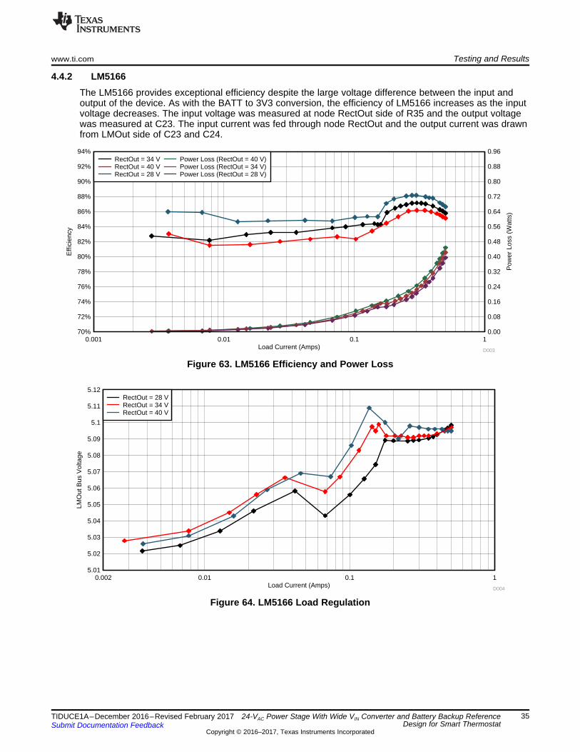
4.4.2 LM5166The LM5166 provides exceptional efficiency despite the large voltage difference between the input andoutput of the device. As with the BATT to 3V3 conversion, the efficiency of LM5166 increases as the inputvoltage decreases. The input voltage was measured at node RectOut side of R35 and the output voltagewas measured at C23. The input current was fed through node RectOut and the output current was drawnfrom LMOut side of C23 and C24.
Figure 63. LM5166 Efficiency and Power Loss
Figure 64. LM5166 Load Regulation
Design Files www.ti.com
36 TIDUCE1A–December 2016–Revised February 2017Submit Documentation Feedback
Copyright © 2016–2017, Texas Instruments Incorporated
24-VAC Power Stage With Wide VIN Converter and Battery Backup ReferenceDesign for Smart Thermostat
5 Design Files
5.1 SchematicsTo download the schematics, see the design files at TIDA-01358.
5.2 Bill of MaterialsTo download the bill of materials (BOM), see the design files at TIDA-01358.
5.3 PCB Layout Recommendations
5.3.1 Layout PrintsTo download the layer plots, see the design files at TIDA-01358.
5.4 Altium ProjectTo download the Altium project files, see the design files at TIDA-01358.
5.5 Gerber FilesTo download the Gerber files, see the design files at TIDA-01358.
5.6 Assembly DrawingsTo download the assembly drawings, see the design files at TIDA-01358.
6 Related Documentation
1. Texas Instruments, Self-Powered AC Solid State Relay With MOSFETs Reference Design ,TIDA-00377 Design Guide (TIDUBR5)
2. Texas Instruments, Low Cost AC Solid State Relay With MOSFETs Reference Design, TIDA-01064Design Guide (TIDUC87)
3. Texas Instruments, Humidity and Temperature Sensor Node for Star Networks Enabling 10+ Year CoinCell Battery Life, TIDA-00374 Design Guide (TIDU797)
4. Texas Instruments, Controlling Output Ripple and Achieving ESR Independence in Constant On-Time(COT) Regulator Designs, Application Note (SNVA166)
5. Texas Instruments, LM5166 3-V to 65-V Input, 500-mA Synchronous Buck Converter with Ultra-LowIQ, LM5166 Datasheet (SNVSA67)
6. Texas Instruments, bq2407x 1.5-A USB-Friendly Li-Ion Battery Charger and Power-Path ManagementIC, bq24072 Datasheet (SLUS810)
7. Texas Instruments, TLV6208x 1.2-A and 2-A High-Efficiency Step-Down Converter in 2-mm × 2-mmWSON Package, TLV62080 Datasheet (SLVSAK9)
8. Texas Instruments, TPS27081A 1.2-V to 8-V, 3-A PFET High-Side Load Switch With Level Shift andAdjustable Slew Rate Control, TPS27081A Datasheet (SLVSBE9)
9. Texas Instruments, LMx93, LM2903 Dual Differential Comparators, LM2903 Datasheet (SLCS005)10. Texas Instruments, TPD2E2U06 Dual-Channel High-Speed ESD Protection Device, TPD2E2U06
Datasheet (SLLSEG9)11. Texas Instruments, TPD1E10B06 Single-Channel ESD Protection Diode in 0402 Package,
TPD1E10B06 Datasheet (SLLSEB1)

www.ti.com About the Author
37TIDUCE1A–December 2016–Revised February 2017Submit Documentation Feedback
Copyright © 2016–2017, Texas Instruments Incorporated
24-VAC Power Stage With Wide VIN Converter and Battery Backup ReferenceDesign for Smart Thermostat
6.1 TrademarksAll trademarks are the property of their respective owners.
7 About the AuthorCASSIDY AARSTAD is a systems designer at Texas Instruments, where he is responsible for developingreference design solutions for the industrial segment. Cassidy earned his master of science in electricalengineering (MSEE) from California Polytechnic State University in San Luis Obispo, California.

Revision A History www.ti.com
38 TIDUCE1A–December 2016–Revised February 2017Submit Documentation Feedback
Copyright © 2016–2017, Texas Instruments Incorporated
Revision History
Revision A HistoryNOTE: Page numbers for previous revisions may differ from page numbers in the current version.
Changes from Original (December 2016) to A Revision ................................................................................................ Page
• Changed language and images to fit current style guide ............................................................................ 1

IMPORTANT NOTICE FOR TI DESIGN INFORMATION AND RESOURCES
Texas Instruments Incorporated (‘TI”) technical, application or other design advice, services or information, including, but not limited to,reference designs and materials relating to evaluation modules, (collectively, “TI Resources”) are intended to assist designers who aredeveloping applications that incorporate TI products; by downloading, accessing or using any particular TI Resource in any way, you(individually or, if you are acting on behalf of a company, your company) agree to use it solely for this purpose and subject to the terms ofthis Notice.TI’s provision of TI Resources does not expand or otherwise alter TI’s applicable published warranties or warranty disclaimers for TIproducts, and no additional obligations or liabilities arise from TI providing such TI Resources. TI reserves the right to make corrections,enhancements, improvements and other changes to its TI Resources.You understand and agree that you remain responsible for using your independent analysis, evaluation and judgment in designing yourapplications and that you have full and exclusive responsibility to assure the safety of your applications and compliance of your applications(and of all TI products used in or for your applications) with all applicable regulations, laws and other applicable requirements. Yourepresent that, with respect to your applications, you have all the necessary expertise to create and implement safeguards that (1)anticipate dangerous consequences of failures, (2) monitor failures and their consequences, and (3) lessen the likelihood of failures thatmight cause harm and take appropriate actions. You agree that prior to using or distributing any applications that include TI products, youwill thoroughly test such applications and the functionality of such TI products as used in such applications. TI has not conducted anytesting other than that specifically described in the published documentation for a particular TI Resource.You are authorized to use, copy and modify any individual TI Resource only in connection with the development of applications that includethe TI product(s) identified in such TI Resource. NO OTHER LICENSE, EXPRESS OR IMPLIED, BY ESTOPPEL OR OTHERWISE TOANY OTHER TI INTELLECTUAL PROPERTY RIGHT, AND NO LICENSE TO ANY TECHNOLOGY OR INTELLECTUAL PROPERTYRIGHT OF TI OR ANY THIRD PARTY IS GRANTED HEREIN, including but not limited to any patent right, copyright, mask work right, orother intellectual property right relating to any combination, machine, or process in which TI products or services are used. Informationregarding or referencing third-party products or services does not constitute a license to use such products or services, or a warranty orendorsement thereof. Use of TI Resources may require a license from a third party under the patents or other intellectual property of thethird party, or a license from TI under the patents or other intellectual property of TI.TI RESOURCES ARE PROVIDED “AS IS” AND WITH ALL FAULTS. TI DISCLAIMS ALL OTHER WARRANTIES ORREPRESENTATIONS, EXPRESS OR IMPLIED, REGARDING TI RESOURCES OR USE THEREOF, INCLUDING BUT NOT LIMITED TOACCURACY OR COMPLETENESS, TITLE, ANY EPIDEMIC FAILURE WARRANTY AND ANY IMPLIED WARRANTIES OFMERCHANTABILITY, FITNESS FOR A PARTICULAR PURPOSE, AND NON-INFRINGEMENT OF ANY THIRD PARTY INTELLECTUALPROPERTY RIGHTS.TI SHALL NOT BE LIABLE FOR AND SHALL NOT DEFEND OR INDEMNIFY YOU AGAINST ANY CLAIM, INCLUDING BUT NOTLIMITED TO ANY INFRINGEMENT CLAIM THAT RELATES TO OR IS BASED ON ANY COMBINATION OF PRODUCTS EVEN IFDESCRIBED IN TI RESOURCES OR OTHERWISE. IN NO EVENT SHALL TI BE LIABLE FOR ANY ACTUAL, DIRECT, SPECIAL,COLLATERAL, INDIRECT, PUNITIVE, INCIDENTAL, CONSEQUENTIAL OR EXEMPLARY DAMAGES IN CONNECTION WITH ORARISING OUT OF TI RESOURCES OR USE THEREOF, AND REGARDLESS OF WHETHER TI HAS BEEN ADVISED OF THEPOSSIBILITY OF SUCH DAMAGES.You agree to fully indemnify TI and its representatives against any damages, costs, losses, and/or liabilities arising out of your non-compliance with the terms and provisions of this Notice.This Notice applies to TI Resources. Additional terms apply to the use and purchase of certain types of materials, TI products and services.These include; without limitation, TI’s standard terms for semiconductor products http://www.ti.com/sc/docs/stdterms.htm), evaluationmodules, and samples (http://www.ti.com/sc/docs/sampterms.htm).
Mailing Address: Texas Instruments, Post Office Box 655303, Dallas, Texas 75265Copyright © 2017, Texas Instruments Incorporated